

Datasheet MIC5219-2.5BM5, MIC5219-2.6BM5, MIC5219-2.7BM5, MIC5219-2.85BM5, MIC5219-2.8BM5 Datasheet (Micrel) [ru]
...
Micrel, Inc. MIC5219
1
2
3
4
8
7
6
5
MIC5219-5.0BMM
2.2µF
tantalum
V
OUT
5V
VIN6V
ENABLE
SHUTDOWN
470pF
15
2
3
4
2.2µF
tantalum
470pF
V
OUT
3.3V
MIC5219-3.3BM5
VIN4V
ENABLE
SHUTDOWN
ENABLE
SHUTDOWN
MIC5219-x.xYML
1
EN
6
C
BYP
(optional)
V
IN
V
OUT
C
OUT
5
4
2
3
ENABLE
SHUTDOWN
MIC5219YMT
1
EN
6
470pF
V
IN
V
OUT
2.2µF
5
4
2
3
R1
R2
+
MIC5219
500mA-Peak Output LDO Regulator
General Description
The MIC5219 is an efcient linear voltage regulator with high
peak output current capability, very-low-dropout voltage, and
better than 1% output voltage accuracy. Dropout is typically
10mV at light loads and less than 500mV at full load.
The MIC5219 is designed to provide a peak output current for
start-up conditions where higher inrush current is demanded.
It features a 500mA peak output rating. Continuous output
current is limited only by package and layout.
The MIC5219 can be enabled or shut down by a CMOS or
TTL compatible signal. When disabled, power consumption
drops nearly to zero. Dropout ground current is minimized to
help prolong battery life. Other key features include reversedbattery protection, current limiting, overtemperature shutdown,
and low noise performance with an ultra-low-noise option.
The MIC5219 is available in adjustable or xed output voltages in the space-saving 6-pin (2mm × 2mm) MLF®, 6-pin
(2mm × 2mm) Thin MLF® SOT-23-5 and MM8® 8-pin power
MSOP packages. For higher power requirements see the
MIC5209 or MIC5237.
All support documentation can be found on Micrel’s web site
at www.micrel.com.
Features
• 500mA output current capability
SOT-23-5 package - 500mA peak
2mm×2mm MLF® package - 500mA continuous
2mm×2mm Thin MLF® package - 500mA
continuous
MSOP-8 package - 500mA continuous
• Low 500mV maximum dropout voltage at full load
• Extremely tight load and line regulation
• Tiny SOT-23-5 and MM8™ power MSOP-8 package
• Ultra-low-noise output
• Low temperature coefcient
• Current and thermal limiting
• Reversed-battery protection
• CMOS/TTL-compatible enable/shutdown control
• Near-zero shutdown current
Applications
• Laptop, notebook, and palmtop computers
• Cellular telephones and battery-powered equipment
• Consumer and personal electronics
• PC Card VCC and VPP regulation and switching
• SMPS post-regulator/DC-to-DC modules
• High-efciency linear power supplies
Typical Applications
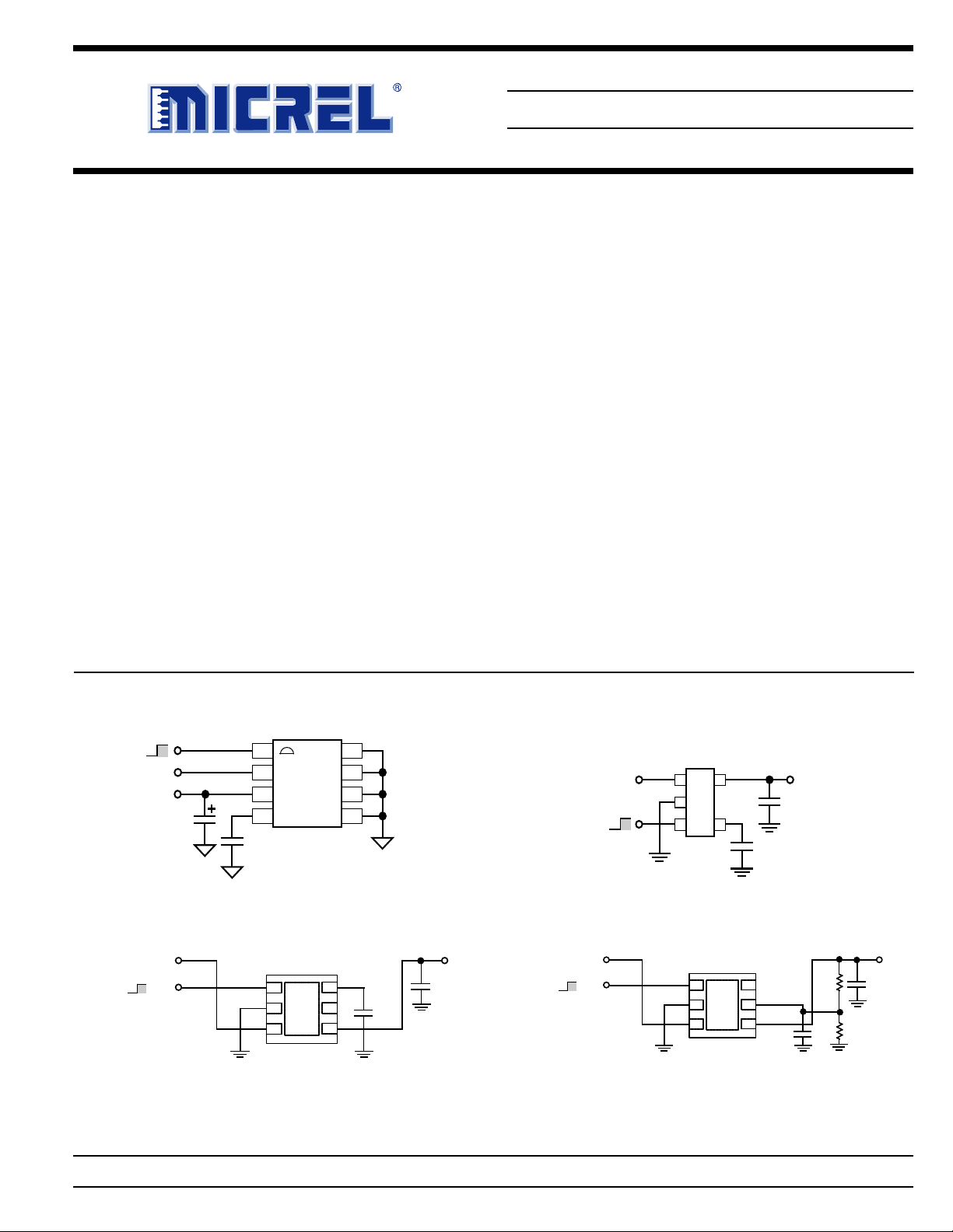
5V Ultra-Low-Noise Regulator
Ultra-Low-Noise Regulator (Fixed)
MM8 is a registered trademark of Micrel, Inc.
MicroLeadFrame and MLF are registered trademarks of Amkor Technology, Inc..
Micrel, Inc. • 2180 Fortune Drive • San Jose, CA 95131 • USA • tel + 1 (408) 944-0800 • fax + 1 (408) 474-1000 • http://www.micrel.com
June 2009 1 M0371-061809
3.3V Ultra-Low-Noise Regulator
Ultra-Low-Noise Regulator (Adjustable)
Micrel, Inc. MIC5219
1
2
3
4
8
7
6
5
GND
GND
GND
GND
EN
IN
OUT
BYP
1
2
3
4
8
7
6
5
GND
GND
GND
GND
EN
IN
OUT
BYP
IN
OUTBYP
EN
LGxx
13
4 5
2
GND
Part
Identification
IN
OUTADJ
EN
LGAA
13
45
2
GND
1EN
GND
IN
6 BYP
NC
OUT
5
4
2
3
1EN
GND
IN
6 NC
ADJ
OUT
5
4
2
3
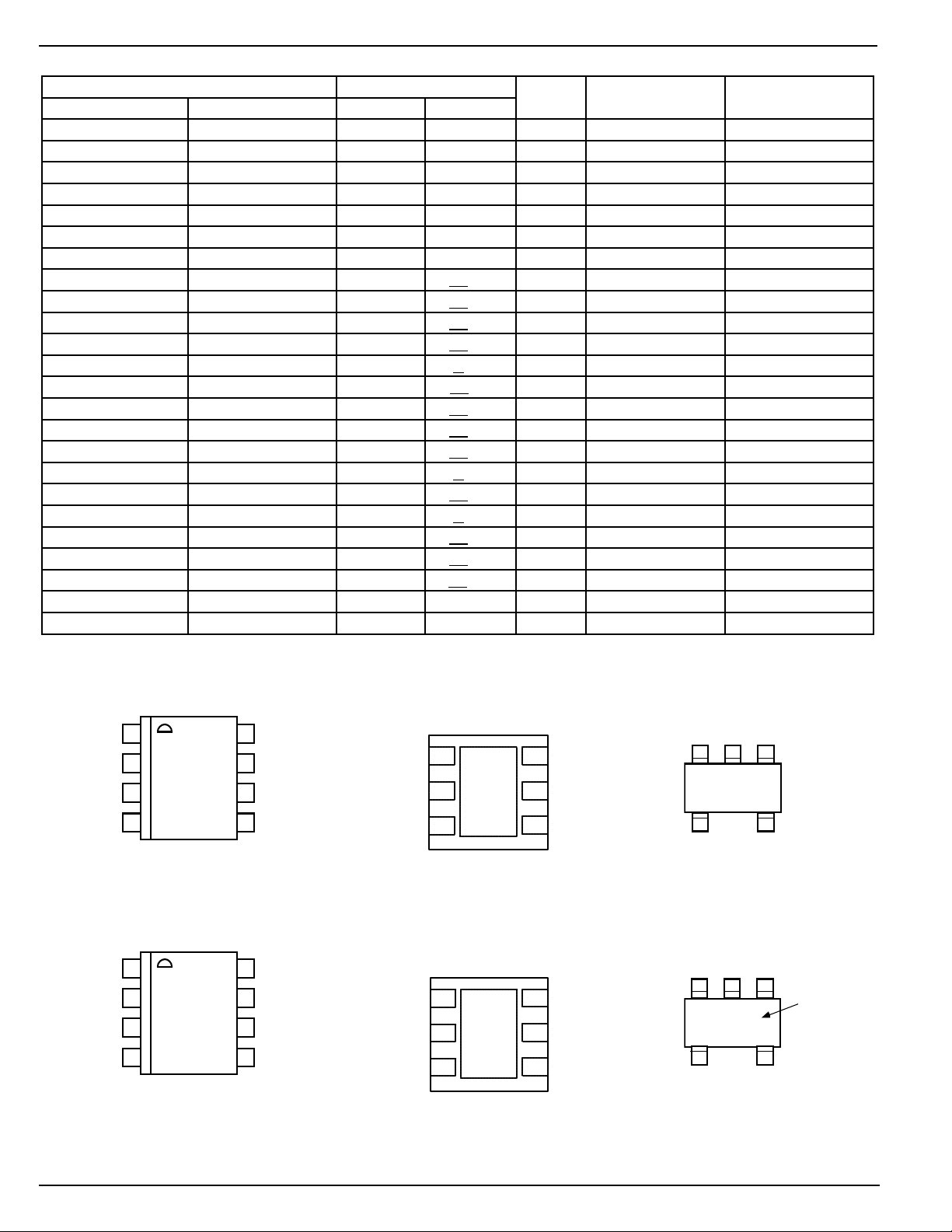
Ordering Information
Part Number Marking
Standard Pb-Free Standard Pb-Free* Volts Temp. Range Package
MIC5219-2.5BMM MIC5219-2.5YMM — — 2.5V –40°C to +125°C MSOP-8
MIC5219-2.85BMM MIC5219-2.85YMM — — 2.85V –40°C to +125°C MSOP-8
MIC5219-3.0BMM MIC5219-3.0YMM — — 3.0V –40°C to +125°C MSOP-8
MIC5219-3.3BMM MIC5219-3.3YMM — — 3.3V –40°C to +125°C MSOP-8
MIC5219-3.6BMM MIC5219-3.6YMM — — 3.6V –40°C to +125°C MSOP-8
MIC5219-5.0BMM MIC5219-5.0YMM — — 5.0V –40°C to +125°C MSOP-8
MIC5219BMM MIC5219YMM — — Adj. –40°C to +125°C MSOP-8
MIC5219-2.5BM5 MIC5219-2.5YM5 LG25 LG25 2.5V –40°C to +125°C SOT-23-5
MIC5219-2.6BM5 MIC5219-2.6YM5 LG26 LG26 2.6V –40°C to +125°C SOT-23-5
MIC5219-2.7BM5 MIC5219-2.7YM5 LG27 LG27 2.7V –40°C to +125°C SOT-23-5
MIC5219-2.8BM5 MIC5219-2.8YM5 LG28 LG28 2.8V –40°C to +125°C SOT-23-5
MIC5219-2.8BML MIC5219-2.8YML G28 G28 2.8V –40°C to +125°C 6-Pin 2×2 MLF
MIC5219-2.85BM5 MIC5219-2.85YM5 LG2J LG2J 2.85V –40°C to +125°C SOT-23-5
MIC5219-2.9BM5 MIC5219-2.9YM5 LG29 LG29 2.9V –40°C to +125°C SOT-23-5
MIC5219-3.1BM5 MIC5219-3.1YM5 LG31 LG31 3.1V –40°C to +125°C SOT-23-5
MIC5219-3.0BM5 MIC5219-3.0YM5 LG30 LG30 3.0V –40°C to +125°C SOT-23-5
MIC5219-3.0BML MIC5219-3.0YML G30 G30 3.0V –40°C to +125°C 6-Pin 2×2 MLF
MIC5219-3.3BM5 MIC5219-3.3YM5 LG33 LG33 3.3V –40°C to +125°C SOT-23-5
MIC5219-3.3BML MIC5219-3.3YML G33 G33 3.3V –40°C to +125°C 6-Pin 2×2 MLF
MIC5219-3.6BM5 MIC5219-3.6YM5 LG36 LG36 3.6V –40°C to +125°C SOT-23-5
MIC5219-5.0BM5 MIC5219-5.0YM5 LG50 LG50 5.0V –40°C to +125°C SOT-23-5
MIC5219BM5 MIC5219YM5 LGAA LGAA Adj. –40°C to +125°C SOT-23-5
MIC5219YMT GAA Adj. –40°C to +125°C 6-Pin 2x2 Thin MLF
MIC5219-5.0YMT G50 5.0V –40°C to +125°C 6-Pin 2x2 Thin MLF
Other voltages available. Consult Micrel for details.
* Over/underbar may not be to scale. ** Pin 1 identier = ▲.
®
®
®
®**
®**
Pin Conguration
MIC5219-x.xBMM / MM8® / MSOP-8
Fixed Voltages
(Top View)
June 2009 2 M0371-061809
MIC5219YMM / MIC5219BMM
Adjustable Voltage
MM8® MSOP-8
(Top View)
6-Pin 2mm × 2mm Thin MLF® (MT)
MIC5219-x.xBML
6-Pin 2mm × 2mm MLF® (ML)
(Top View)
MIC5219YMT
(Top View)
MIC5219-x.xBM5 / SOT-23-5
Fixed Voltages
(Top View)
MIC5219BM5 / SOT-23-5
Adjustable Voltage
(Top View)
Micrel, Inc. MIC5219
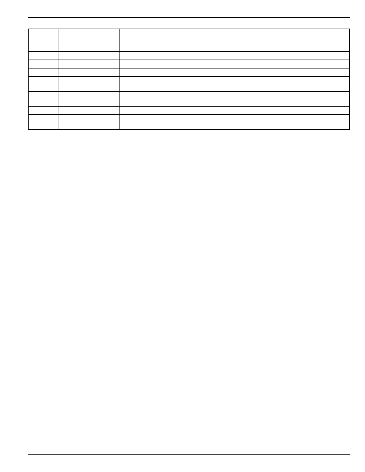
Pin Description
Pin No. Pin No. Pin No. Pin Name Pin Function
MLF-6 MSOP-8 SOT-23-5
TMLF-6
3 2 1 IN Supply Input.
2 5–8 2 GND Ground: MSOP-8 pins 5 through 8 are internally connected.
4 3 5 OUT Regulator Output.
1 1 3 EN Enable (Input): CMOS compatible control input. Logic high = enable; logic
low or open = shutdown.
6 4 (xed) 4 (xed) BYP Reference Bypass: Connect external 470pF capacitor to GND to reduce
output noise. May be left open.
5(NC) 4 (adj.) 4 (adj.) ADJ Adjust (Input): Feedback input. Connect to resistive voltage-divider network.
EP — — GND Ground: Internally connected to the exposed pad. Connect externally to
GND pin.
June 2009 3 M0371-061809
Micrel, Inc. MIC5219
nV/ Hz
nV/ Hz
Absolute Maximum Ratings
(1)
Supply Input Voltage (VIN) ..............................–20V to +20V
Power Dissipation (PD) ............................. Internally Limited
Junction Temperature (TJ) ........................ –40°C to +125°C
Storage Temperature (TS) ........................ –65°C to +150°C
Operating Ratings
Supply Input Voltage (VIN) ............................ +2.5V to +12V
Enable Input Voltage (VEN)....................................0V to V
Junction Temperature (TJ) ........................ –40°C to +125°C
Package Thermal Resistance ........................... see Table 1
(2)
Lead Temperature (Soldering, 5 sec.) ....................... 260°C
IN
Electrical Characteristics
VIN = V
+ 1.0V; C
OUT
= 4.7µF, I
OUT
(3)
= 100µA; TJ = 25°C, bold values indicate –40°C ≤ TJ ≤ +125°C; unless noted.
OUT
Symbol Parameter Conditions Min Typical Max Units
Output Voltage Accuracy variation from nominal V
V
OUT
–1 1 %
OUT
–2 2 %
/ΔT Output Voltage Note 4 40
ΔV
OUT
ppm/°C
Temperature Coefcient
ΔV
OUT/VOUT
Line Regulation VIN = V
+ 1V to 12V 0.009 0.05 %/V
OUT
0.1
ΔV
OUT/VOUT
Load Regulation I
= 100µA to 500mA, Note 5 0.05 0.5 %
OUT
0.7
– V
V
IN
OUT
Dropout Voltage
(6)
I
= 100µA 10 60 mV
OUT
80
I
= 50mA 115 175 mV
OUT
250
I
= 150mA 175 300 mV
OUT
400
I
= 500mA 350 500 mV
OUT
600
Ground Pin Current
I
GND
(7, 8)
V
≥ 3.0V, I
EN
= 100µA 80 130 µA
OUT
170
V
≥ 3.0V, I
EN
= 50mA 350 650 µA
OUT
900
V
≥ 3.0V, I
EN
= 150mA 1.8 2.5 mA
OUT
3.0
V
≥ 3.0V, I
EN
= 500mA 12 20 mA
OUT
25
(8)
Ground Pin Quiescent Current
V
VEN ≤ 0.4V 0.05 3 µA
≤ 0.18V 0.10 8 µA
EN
PSRR Ripple Rejection f = 120Hz 75 dB
Current Limit V
I
LIMIT
/ΔPD Thermal Regulation Note 9 0.05 %/W
ΔV
OUT
Output Noise
e
no
(10)
I
I
= 0V 700 1000 mA
OUT
= 50mA, C
OUT
= 50mA, C
OUT
= 2.2µF, C
OUT
= 2.2µF, C
OUT
= 0 500
BYP
= 470pF 300
BYP
ENABLE Input
Enable Input Logic-Low Voltage VEN = logic low (regulator shutdown) 0.4 V
V
ENL
0.18
V
Enable Input Current V
I
ENL
V
V
I
ENH
= logic high (regulator enabled) 2.0 V
EN
≤ 0.4V 0.01 –1 µA
ENL
≤ 0.18V 0.01 –2 µA
ENL
≥ 2.0V 2 5 20 µA
ENH
25
June 2009 4 M0371-061809

Micrel, Inc. MIC5219
Notes:
1. Absolute maximum ratings indicate limits beyond which damage to the component may occur. Electrical specications do not apply when operating
the device outside of its operating ratings. The maximum allowable power dissipation is a function of the maximum junction temperature, TJ(max),
the junction-to-ambient thermal resistance, θ
temperature is calculated using: PD(max) = (TJ(max) – TA) ÷ θJA. Exceeding the maximum allowable power dissipation will result in excessive die
temperature, and the regulator will go into thermal shutdown. See Table 1 and the “Thermal Considerations” section for details.
2. The device is not guaranteed to function outside its operating rating.
3. Specication for packaged product only.
4. Output voltage temperature coefcient is dened as the worst case voltage change divided by the total temperature range.
5. Regulation is measured at constant junction temperature using low duty cycle pulse testing. Parts are tested for load regulation in the load range
from 100µA to 500mA. Changes in output voltage due to heating effects are covered by the thermal regulation specication.
6. Dropout voltage is dened as the input to output differential at which the output voltage drops 2% below its nominal value measured at 1V differential.
7. Ground pin current is the regulator quiescent current plus pass transistor base current. The total current drawn from the supply is the sum of the load
current plus the ground pin current.
is the voltage externally applied to devices with the EN (enable) input pin.
8. V
EN
9. Thermal regulation is dened as the change in output voltage at a time “t” after a change in power dissipation is applied, excluding load or line regulation effects. Specications are for a 500mA load pulse at V
10. C
is an optional, external bypass capacitor connected to devices with a BYP (bypass) or ADJ (adjust) pin.
BYP
, and the ambient temperature, TA. The maximum allowable power dissipation at any ambient
JA
= 12V for t = 10ms.
IN
June 2009 5 M0371-061809

Micrel, Inc. MIC5219
-100
-80
-60
-40
-20
0
1E+1 1E+2 1E+3 1E+4 1E+5 1E+6 1E+7
FREQUENCY (Hz)
Power Supply
Rejection Ratio
I
OUT
= 100µA
C
OUT
= 1µF
VIN = 6V
V
OUT
= 5V
10 100
1k
10k
100k
1M 10M
-100
-80
-60
-40
-20
0
1E+1 1E+2 1E+3 1E+4 1E+5 1E+6 1E+7
FREQUENCY (Hz)
Power Supply
Rejection Ratio
I
OUT
= 1mA
C
OUT
= 1µF
VIN = 6V
V
OUT
= 5V
10 100
1k
10k
100k
1M 10M
-100
-80
-60
-40
-20
0
1E+1 1E+2 1E+3 1E+4 1E+5 1E+6 1E+7
FREQUENCY (Hz)
Power Supply
Rejection Ratio
I
OUT
= 100mA
C
OUT
= 1µF
VIN = 6V
V
OUT
= 5V
10 100
1k
10k
100k
1M 10M
-100
-80
-60
-40
-20
0
1E+1 1E+2 1E+3 1E+4 1E+5 1E+6 1E+7
FREQUENCY (Hz)
Power Supply
Rejection Ratio
I
OUT
= 100µA
C
OUT
= 2.2µF
C
BYP
= 0.01µF
VIN = 6V
V
OUT
= 5V
10 100
1k
10k
100k
1M 10M
-100
-80
-60
-40
-20
0
1E+1 1E+2 1E+3 1E+4 1E+5 1E+6 1E+7
FREQUENCY (Hz)
Power Supply
Rejection Ratio
I
OUT
= 1mA
C
OUT
= 2.2µF
C
BYP
= 0.01µF
VIN = 6V
V
OUT
= 5V
10 100
1k
10k
100k
1M 10M
0
10
20
30
40
50
60
0 0.1 0.2 0.3 0.4
VOLTAGE DROP (V)
Power Supply Ripple Rejection
vs. Voltage Drop
I
OUT
= 100mA
10mA
1mA
C
OUT
= 1µF
0
10
20
30
40
50
60
70
80
90
100
0 0.1 0.2 0.3 0.4
VOLTAGE DROP (V)
Power Supply Ripple Rejection
vs. Voltage Drop
I
OUT
= 100mA
10mA
1mA
C
OUT
= 2.2µF
C
BYP
= 0.01µF
0.0001
0.001
0.01
0.1
1
10
1E+1 1E+2 1E+3 1E+4 1E+5 1E+6 1E+7
FREQUENCY (Hz)
Noise Performance
10
100
1k
10k 100k 1M 10M
10mA, C
OUT
= 1µF
V
OUT
= 5V
0.0001
0.001
0.01
0.1
1
10
1E+1 1E+2 1E+3 1E+4 1E+5 1E+6 1E+7
FREQUENCY (Hz)
Noise Performance
10mA
1mA
100mA
10
100
1k
10k 100k 1M 10M
V
OUT
= 5V
C
OUT
= 10µF
electrolytic
0.0001
0.001
0.01
0.1
1
10
1E+1 1E+2 1E+3 1E+4 1E+5 1E+6 1E+7
FREQUENCY (Hz)
Noise Performance
10mA
1mA
100mA
10
100
1k
10k 100k 1M 10M
V
OUT
= 5V
C
OUT
= 10µF
electrolytic
C
BYP
= 100pF
0
100
200
300
400
0 100 200 300 400 500
OUTPUT CURRENT (mA)
Dropout Voltage
vs. Output Current
0
0.5
1.0
1.5
2.0
2.5
3.0
3.5
0 1 2 3 4 5 6 7 8 9
INPUT VOLTAGE (V)
Dropout Characteristics
IL =100µA
IL=100mA
IL=500mA
Typical Characteristics
June 2009 6 M0371-061809

Micrel, Inc. MIC5219
0
2
4
6
8
10
12
0 100 200 300 400 500
OUTPUT CURRENT (mA)
Ground Current
vs. Output Current
0
0.5
1.0
1.5
2.0
2.5
3.0
0 2 4 6 8
INPUT VOLTAGE (V)
Ground Current
vs. Supply Voltage
IL=100 mA
IL=100µA
0
5
10
15
20
25
0 1 2 3 4 5 6 7 8 9
INPUT VOLTAGE (V)
Ground Current
vs. Supply Voltage
IL=500mA
June 2009 7 M0371-061809

Micrel, Inc. MIC5219
IN
EN
OUT
BYP
C
BYP
(optional)
GND
V
REF
Bandgap
Ref.
Current Limit
Thermal Shutdown
C
OUT
V
OUT
V
IN
MIC5219-x.xBM5/M/YMT
IN
EN
OUT
C
BYP
(optional)
GND
V
REF
Bandgap
Ref.
Current Limit
Thermal Shutdown
C
OUT
V
OUT
V
IN
R1
R2
MIC5219BM5/MM/YMT
Block Diagrams
Ultra-Low-Noise Fixed Regulator
Ultra-Low-Noise Adjustable Regulator
June 2009 8 M0371-061809

Micrel, Inc. MIC5219
PD(max ) =
TJ(max ) − T
A
( )
θ
JA
PD(max ) =
125 °C − 25°C
( )
220°C / W
Applications Information
The MIC5219 is designed for 150mA to 200mA output current
applications where a high current spike (500mA) is needed for
short, start-up conditions. Basic application of the device will
be discussed initially followed by a more detailed discussion
of higher current applications.
Enable/Shutdown
Forcing EN (enable/shutdown) high (>2V) enables the
regulator. EN is compatible with CMOS logic. If the enable/
shutdown feature is not required, connect EN to IN (supply
input). See Figure 5.
Input Capacitor
A 1µF capacitor should be placed from IN to GND if there is
more than 10 inches of wire between the input and the AC
lter capacitor or if a battery is used as the input.
Output Capacitor
An output capacitor is required between OUT and GND to
prevent oscillation. The minimum size of the output capacitor
is dependent upon whether a reference bypass capacitor is
used. 1µF minimum is recommended when C
(see Figure 5). 2.2µF minimum is recommended when C
is 470pF (see Figure 6). For applications < 3V, the output
capacitor should be increased to 22µF minimum to reduce
start-up overshoot. Larger values improve the regulator’s
transient response. The output capacitor value may be increased without limit.
The output capacitor should have an ESR (equivalent series
resistance) of about 1Ω or less and a resonant frequency
above 1MHz. Ultra-low-ESR capacitors could cause oscillation and/or underdamped transient response. Most tantalum
or aluminum electrolytic capacitors are adequate; lm types
will work, but are more expensive. Many aluminum electrolytics have electrolytes that freeze at about –30°C, so solid
tantalums are recommended for operation below –25°C.
At lower values of output current, less output capacitance is
needed for stability. The capacitor can be reduced to 0.47µF
for current below 10mA, or 0.33µF for currents below 1mA.
No-Load Stability
The MIC5219 will remain stable and in regulation with no load
(other than the internal voltage divider) unlike many other
voltage regulators. This is especially important in CMOS
RAM keep-alive applications.
Reference Bypass Capacitor
BYP is connected to the internal voltage reference. A 470pF
capacitor (C
) connected from BYP to GND quiets this
BYP
reference, providing a signicant reduction in output noise
(ultra-low-noise performance). C
phase margin; when using C
BYP
reduces the regulator
BYP
, output capacitors of 2.2µF
or greater are generally required to maintain stability.
The start-up speed of the MIC5219 is inversely proportional
to the size of the reference bypass capacitor. Applications
requiring a slow ramp-up of output voltage should consider
larger values of C
consider omitting C
. Likewise, if rapid turn-on is necessary,
BYP
.
BYP
is not used
BYP
BYP
Thermal Considerations
The MIC5219 is designed to provide 200mA of continuous
current in two very small prole packages. Maximum power
dissipation can be calculated based on the output current and
the voltage drop across the part. To determine the maximum
power dissipation of the package, use the thermal resistance,
junction-to-ambient, of the device and the following basic
equation.
TJ(max) is the maximum junction temperature of the die,
125°C, and TA is the ambient operating temperature. θJA
is layout dependent; Table 1 shows examples of thermal
resistance, junction-to-ambient, for the MIC5219.
Package θJA Recommended θJA 1" SquareθJC
Minimum Footprint 2oz. Copper
®
(MM) 160°C/W 70°C/W 30°C/W
MM8
SOT-23-5 (M5) 220°C/W 170°C/W 130°C/W
®
(ML) 90°C/W — —
®
(MT) 90°C/W — —
2×2 MLF
2×2 Thin
MLF
Table 1. MIC5219 Thermal Resistance
The actual power dissipation of the regulator circuit can be
determined using one simple equation.
PD = (VIN – V
OUT
) I
OUT
+ VIN I
GND
Substituting PD(max) for PD and solving for the operating
conditions that are critical to the application will give the
maximum operating conditions for the regulator circuit. For
example, if we are operating the MIC5219-3.3BM5 at room
temperature, with a minimum footprint layout, we can determine the maximum input voltage for a set output current.
PD(max) = 455mW
The thermal resistance, junction-to-ambient, for the minimum
footprint is 220°C/W, taken from Table 1. The maximum power
dissipation number cannot be exceeded for proper operation of the device. Using the output voltage of 3.3V, and an
output current of 150mA, we can determine the maximum
input voltage. Ground current, maximum of 3mA for 150mA
of output current, can be taken from the “Electrical Characteristics” section of the data sheet.
455mW = (VIN – 3.3V) × 150mA + VIN × 3mA
455mW = (150mA) × VIN + 3mA × VIN – 495mW
950mW = 153mA × V
VIN = 6.2V
MAX
IN
Therefore, a 3.3V application at 150mA of output current
can accept a maximum input voltage of 6.2V in a SOT-23-5
package. For a full discussion of heat sinking and thermal
effects on voltage regulators, refer to the “Regulator Thermals” section of Micrel’s Designing with Low-Dropout Voltage
Regulators handbook.
June 2009 9 M0371-061809

Micrel, Inc. MIC5219
PD(max ) =
TJ(max ) − T
A
( )
θ
JA
PD(max ) =
125 °C − 25°C
( )
220 °C /W
VIN(max ) =
2.955W
520mA
= 5.683V
Avg.PD=
% DC
100
VIN – V
OUT
( )
I
OUT+VIN IGND
455mW =
% DC
100
8V – 5V
( )
500mA + 8V ×20mA
455mW =
% Duty Cycle
100
1.66W
0.274 =
% Duty Cycle
100
% Duty Cycle Max = 27.4%
Peak Current Applications
The MIC5219 is designed for applications where high start-up
currents are demanded from space constrained regulators.
This device will deliver 500mA start-up current from a SOT23-5 or MM8 package, allowing high power from a very low
prole device. The MIC5219 can subsequently provide output
current that is only limited by the thermal characteristics of
the device. You can obtain higher continuous currents from
the device with the proper design. This is easily proved with
some thermal calculations.
If we look at a specic example, it may be easier to follow.
The MIC5219 can be used to provide up to 500mA continuous
output current. First, calculate the maximum power dissipation of the device, as was done in the thermal considerations
section. Worst case thermal resistance (θ
the MIC5219-x.xBM5), will be used for this example.
Assuming a 25°C room temperature, we have a maximum
power dissipation number of
= 220°C/W for
JA
xBMM, the power MSOP package part. These graphs show
three typical operating regions at different temperatures. The
lower the temperature, the larger the operating region. The
graphs were obtained in a similar way to the graphs for the
MIC5219-x.xBM5, taking all factors into consideration and
using two different board layouts, minimum footprint and 1"
square copper PC board heat sink. (For further discussion
of PC board heat sink characteristics, refer to “Application
Hint 17, Designing PC Board Heat Sinks” .)
The information used to determine the safe operating regions
can be obtained in a similar manner such as determining
typical power dissipation, already discussed. Determining
the maximum power dissipation based on the layout is the
rst step, this is done in the same manner as in the previous
two sections. Then, a larger power dissipation number multiplied by a set maximum duty cycle would give that maximum
power dissipation number for the layout. This is best shown
through an example. If the application calls for 5V at 500mA
for short pulses, but the only supply voltage available is
8V, then the duty cycle has to be adjusted to determine an
average power that does not exceed the maximum power
dissipation for the layout.
PD(max) = 455mW
Then we can determine the maximum input voltage for a
5-volt regulator operating at 500mA, using worst case ground
current.
PD(max) = 455mW = (VIN – V
I
V
I
455mW = (VIN – 5V) 500mA + VIN × 20mA
2.995W = 520mA × V
Therefore, to be able to obtain a constant 500mA output current from the 5219-5.0BM5 at room temperature, you need
extremely tight input-output voltage differential, barely above
the maximum dropout voltage for that current rating.
You can run the part from larger supply voltages if the proper
precautions are taken. Varying the duty cycle using the enable pin can increase the power dissipation of the device by
maintaining a lower average power gure. This is ideal for
applications where high current is only needed in short bursts.
Figure 1 shows the safe operating regions for the MIC5219-x.
xBM5 at three different ambient temperatures and at different output currents. The data used to determine this gure
assumed a minimum footprint PCB design for minimum heat
sinking. Figure 2 incorporates the same factors as the rst
gure, but assumes a much better heat sink. A 1" square copper trace on the PC board reduces the thermal resistance of
the device. This improved thermal resistance improves power
dissipation and allows for a larger safe operating region.
Figures 3 and 4 show safe operating regions for the MIC5219-x.
June 2009 10 M0371-061809
= 500mA
OUT
= 5V
OUT
= 20mA
GND
IN
OUT
) I
OUT
+ VIN I
GND
With an output current of 500mA and a three-volt drop across
the MIC5219-xxBMM, the maximum duty cycle is 27.4%.
Applications also call for a set nominal current output with a
greater amount of current needed for short durations. This is a
tricky situation, but it is easily remedied. Calculate the average
power dissipation for each current section, then add the two
numbers giving the total power dissipation for the regulator.
For example, if the regulator is operating normally at 50mA,
but for 12.5% of the time it operates at 500mA output, the
total power dissipation of the part can be easily determined.
First, calculate the power dissipation of the device at 50mA.
We will use the MIC5219-3.3BM5 with 5V input voltage as
our example.
PD × 50mA = (5V – 3.3V) × 50mA + 5V × 650µA
PD × 50mA = 173mW
However, this is continuous power dissipation, the actual
on-time for the device at 50mA is (100%-12.5%) or 87.5%
of the time, or 87.5% duty cycle. Therefore, PD must be multiplied by the duty cycle to obtain the actual average power
dissipation at 50mA.

Micrel, Inc. MIC5219
0
2
4
6
8
10
0 20 40 60 80 100
DUTY CYCLE (%)
500mA
400mA
300mA
200mA
100mA
0
2
4
6
8
10
0 20 40 60 80 100
DUTY CYCLE (%)
500mA
400mA
300mA
200mA
100mA
0
2
4
6
8
10
0 20 40 60 80 100
DUTY CYCLE (%)
500mA
400mA
300mA
200mA
100mA
0
2
4
6
8
10
0 20 40 60 80 100
DUTY CYCLE (%)
500mA
400mA
300mA
200mA
0
2
4
6
8
10
0 20 40 60 80 100
DUTY CYCLE (%)
500mA
400mA
300mA
200mA
100mA
0
2
4
6
8
10
0 20 40 60 80 100
DUTY CYCLE (%)
500mA
400mA
300mA
200mA
100mA
0
2
4
6
8
10
0 20 40 60 80 100
DUTY CYCLE (%)
500mA
400mA
300mA
200mA
100mA
0
2
4
6
8
10
0 20 40 60 80 100
DUTY CYCLE (%)
500mA
400mA
300mA
200mA
0
2
4
6
8
10
0 20 40 60 80 100
DUTY CYCLE (%)
500mA
400mA
300mA
200mA
100mA
0
2
4
6
8
10
0 20 40 60 80 100
DUTY CYCLE (%)
500mA
400mA
300mA
200mA
100mA
0
2
4
6
8
10
0 20 40 60 80 100
DUTY CYCLE (%)
500mA
400mA
300mA
200mA
100mA
0
2
4
6
8
10
0 20 40 60 80 100
DUTY CYCLE (%)
500mA
400mA
300mA
200mA
100mA
a. 25°C Ambient b. 50°C Ambient c. 85°C Ambient
Figure 1. MIC5219-x.xBM5 (SOT-23-5) on Minimum Recommended Footprint
a. 25°C Ambient b. 50°C Ambient c. 85°C Ambient
Figure 2. MIC5219-x.xBM5 (SOT-23-5) on 1-inch2 Copper Cladding
a. 25°C Ambient b. 50°C Ambient c. 85°C Ambient
Figure 3. MIC5219-x.xBMM (MSOP-8) on Minimum Recommended Footprint
a. 25°C Ambient b. 50°C Ambient c. 85°C Ambient
Figure 4. MIC5219-x.xBMM (MSOP-8) on 1-inch2 Copper Cladding
June 2009 11 M0371-061809

Micrel, Inc. MIC5219
MIC5219-x.x
IN OUT
GND
1µF
V
IN
V
OUT
EN BYP
MIC5219-x.x
IN OUT
GND
470pF
V
IN
EN BYP
2.2µF
V
OUT
MIC5219
IN OUT
GND
V
IN
EN ADJ
1µF
V
OUT
R1
R2
V
OUT
=1.242V
R2
R1
+1
MIC5219
IN OUT
GND
V
IN
EN ADJ
2.2µF
V
OUT
R1
R2
470pF
PD × 50mA = 0.875 × 173mW
PD × 50mA = 151mW
The power dissipation at 500mA must also be calculated.
PD × 500mA = (5V – 3.3V) 500mA + 5V × 20mA
PD × 500mA = 950mW
This number must be multiplied by the duty cycle at which it
would be operating, 12.5%.
PD × = 0.125 × 950mW
PD × = 119mW
The total power dissipation of the device under these conditions is the sum of the two power dissipation gures.
P
P
P
= PD × 50mA + PD × 500mA
D(total)
= 151mW + 119mW
D(total)
= 270mW
D(total)
Figure 6. Ultra-Low-Noise Fixed Voltage Regulator
Figure 6 includes the optional 470pF noise bypass capacitor
between BYP and GND to reduce output noise. Note that the
minimum value of C
must be increased when the bypass
OUT
capacitor is used.
Adjustable Regulator Circuits
The total power dissipation of the regulator is less than the
maximum power dissipation of the SOT-23-5 package at room
temperature, on a minimum footprint board and therefore
would operate properly.
Multilayer boards with a ground plane, wide traces near the
pads, and large supply-bus lines will have better thermal
conductivity.
For additional heat sink characteristics, please refer to Micrel “Application Hint 17, Designing P.C. Board Heat Sinks”,
included in Micrel’s Databook. For a full discussion of heat
Figure 7. Low-Noise Adjustable Voltage Regulator
Figure 7 shows the basic circuit for the MIC5219 adjustable
regulator. The output voltage is congured by selecting values
for R1 and R2 using the following formula:
sinking and thermal effects on voltage regulators, refer to
“Regulator Thermals” section of Micrel’s Designing with LowDropout Voltage Regulators handbook.
Fixed Regulator Circuits
Although ADJ is a high-impedance input, for best performance,
R2 should not exceed 470kΩ.
Figure 5. Low-Noise Fixed Voltage Regulator
Figure 5 shows a basic MIC5219-x.xBMX xed-voltage regulator circuit. A 1µF minimum output capacitor is required for
basic xed-voltage applications.
June 2009 12 M0371-061809
Figure 8. Ultra-Low-Noise Adjustable Application
Figure 8 includes the optional 470pF bypass capacitor from
ADJ to GND to reduce output noise.

Micrel, Inc. MIC5219
Package Information
8-Pin MSOP (MM)
SOT-23-5 (M5)
June 2009 13 M0371-061809

Micrel, Inc. MIC5219
6-Pin MLF® (ML)
6-Pin Thin MLF® (MT)
MICREL, INC. 2180 FORTUNE DRIVE SAN JOSE, CA 95131 USA
The information furnished by Micrel in this data sheet is believed to be accurate and reliable. However, no responsibility is assumed by Micrel for its use.
Micrel reserves the right to change circuitry and specications at any time without notication to the customer.
Micrel Products are not designed or authorized for use as components in life support appliances, devices or systems where malfunction of a product can
reasonably be expected to result in personal injury. Life support devices or systems are devices or systems that (a) are intended for surgical implant into
the body or (b) support or sustain life, and whose failure to perform can be reasonably expected to result in a signicant injury to the user. A Purchaser’s
use or sale of Micrel Products for use in life support appliances, devices or systems is at Purchaser’s own risk and Purchaser agrees to fully indemnify
t e l + 1 (408) 944-0800 f a x + 1 (408) 474-1000 w e b http://www.micrel.com
Micrel for any damages resulting from such use or sale.
© 2005 Micrel, Incorporated.
June 2009 14 M0371-061809

 Loading...