

Page 1
Service
SR7500 /
SR8500 /
A1B/A1S/K1G/L1G
/N1B/N1G/N1S/U1B
A1B/A1S/L1G/N1B
/N1G/N1S/U1B
Manual
2nd EDITION
• 1, 25 and 27 pages were changed.
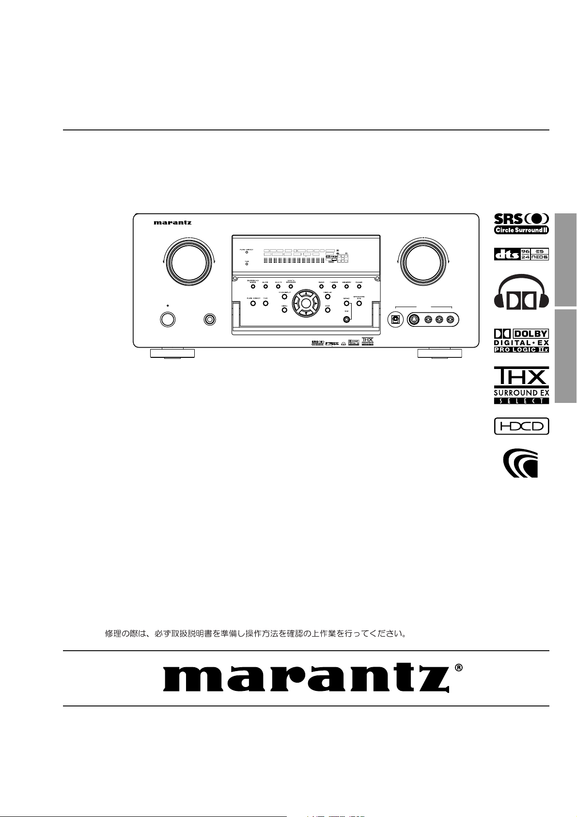
AV SURROUND RECEIVER SR7500
INPUT SELECTOR
DISP MULTI AUT O TUNED ST SPKR A B V-OF F
SLEEP
AUTO
STANDBY
POWER ON/OFF PHONES
TABLE OF CONTENTS
SECTION PAGE
1. TECH NI CAL SPEC I FI CA TIONS ........................................................................................... 1
2. TECHNICAL DESCRIPTION ................................................................................................ 4
3. POWER AMPLIFIER AD JUST MENT ................................................................................... 8
4. SERVICE MODE................................................................................................................... 9
5. SYSTEM ERROR ...............................................................................................................11
6. UPDATE FIRMWARE.......................................................................................................... 12
7. WIRING DI A GRAM ............................................................................................................. 19
8. BLOCK DIAGRAM ..............................................................................................................21
9. SCHEMATIC DIAGRAM...................................................................................................... 23
10. PARTS LOCATION..............................................................................................................45
11. IC DATA............................................................................................................................... 61
12. EXPLODED VIEW AND PARTS LIST................................................................................. 85
13. ELECTRICAL PARTS LIST................................................................................................. 97
SURR DIRECT
DISC 6.1 MTX 6.1
AV Surround Receiver
PS7500 /
PS8500 /
F1N
F1N
AV Surround Amplifi er
VOLUME
SURROUND
PEAK ANALOG
ATT
DIGITAL
DIGITAL
NIGHT
LCR
LFE
AAC
PCM
SL S SR
ENTER
DOWN
UP
PS7500 / PS8500
AUX 1 INPUT
AUDIOS-VIDEODIGITAL VIDEO L R
SR7500 / SR8500
Please use this service manual with referring to the user guide ( D.F.U. ) without fail.
SR7500 / SR8500
PS7500 / PS8500
Part no. 90M10BW855012
2nd Issue 2004.11
MJI
Page 2
MARANTZ DESIGN AND SERVICE
Using superior design and selected high grade components,
Only original
MARANTZ
parts can insure that your
MARANTZ
MARANTZ
product will continue to perform to the specifi cations for which
company has created the ultimate in stereo sound.
it is famous.
Parts for your
MARANTZ
ORDERING PARTS :
equipment are generally available to our National Marantz Subsidiary or Agent.
Parts can be ordered either by mail or by Fax.. In both cases, the correct part number has to be specifi ed.
The following information must be supplied to eliminate delays in processing your order :
1. Complete address
2. Complete part numbers and quantities required
3. Description of parts
4. Model number for which part is required
5. Way of shipment
6. Signature : any order form or Fax. must be signed, otherwise such part order will be considered as null and void.
USA
MARANTZ AMERICA, INC
1100 MAPLEWOOD DRIVE
ITASCA, IL. 60143
USA
PHONE : 630 - 741 - 0300
FAX : 630 - 741 - 0301
AUSTRALIA
QualiFi Pty Ltd,
24 LIONEL ROAD,
MT. WAVERLEY VIC 3149
AUSTRALIA
PHONE : +61 - (0)3 - 9543 - 1522
FAX : +61 - (0)3 - 9543 - 3677
EUROPE / TRADING
MARANTZ EUROPE B.V.
P. O. BOX 8744, BUILDING SILVERPOINT
BEEMDSTRAAT 11, 5653 MA EINDHOVEN
THE NETHERLANDS
PHONE : +31 - 40 - 2507844
FAX : +31 - 40 - 2507860
THAILAND
MRZ STANDARD CO., LTD
746 - 754 MAHACHAI ROAD.,
WANGBURAPAPIROM, PHRANAKORN,
BANGKOK, 10200 THAILAND
PHONE : +66 - 2 - 222 9181
FAX : +66 - 2 - 224 6795
CANADA
MARANTZ CANADA INC.
5-505 APPLE CREEK BLVD.
MARKHAM, ONTARIO L3R 5B1
CANADA
PHONE : 905 - 415 - 9292
FAX : 905 - 475 - 4159
SINGAPORE
WO KEE HONG DISTRIBUTION PTE LTD
No.1 JALAN KILANG TIMOR
#08-03 PACIFIC TECH CENTRE
SINGAPORE 159303
PHONE : +65 6376 0338
FAX : +65 6376 0166
NEW ZEALAND
WILDASH AUDIO SYSTEMS NZ
14 MALVERN ROAD MT ALBERT
AUCKLAND NEW ZEALAND
PHONE : +64 - 9 - 8451958
FAX : +64 - 9 - 8463554
JAPAN
MARANTZ JAPAN, INC.
35- 1, 7- CHOME, SAGAMIONO
SAGAMIHARA - SHI, KANAGAWA
JAPAN 228-8505
PHONE : +81 42 748 1013
FAX : +81 42 741 9190
Technical
TAIWAN
PAI- YUING CO., LTD.
6 TH FL NO, 148 SUNG KIANG ROAD,
TAIPEI, 10429, TAIWAN R.O.C.
PHONE : +886 - 2 - 25221304
FAX : +886 - 2 - 25630415
SHOCK, FIRE HAZARD SERVICE TEST :
MALAYSIA
WO KEE HONG ELECTRONICS SDN. BHD.
2ND FLOOR BANGUNAN INFINITE CENTRE
LOT 1, JALAN 13/6, 46200 PETALING JAYA
SELANGOR DARUL EHSAN, MALAYSIA
PHONE : +60 - 3 - 7954 8088
FAX : +60 - 3 - 7954 7088
KOREA
MK ENTERPRISES LTD.
ROOM 604/605, ELECTRO-OFFICETEL, 16-58,
3GA, HANGANG-RO, YONGSAN-KU, SEOUL
KOREA
PHONE : +822 - 3232 - 155
FAX : +822 - 3232 - 154
CAUTION : After servicing this appliance and prior to returning to customer, measure the resistance between either primary AC
cord connector pins ( with unit NOT connected to AC mains and its Power switch ON ), and the face or Front Panel of product and
controls and chassis bottom.
Any resistance measurement less than 1 Megohms should cause unit to be repaired or corrected before AC power is applied, and
verifi ed before it is return to the user/customer.
Ref. UL Standard No. 1492.
In case of diffi culties, do not hesitate to contact the Technical
Department at above mentioned address.
041015MJI
Page 3

1. TECHNICAL SPECIFICATIONS
FM TUNER SECTION [SR7500/SR8500]
Frequency Range.............................................87.5 - 108.0 MHz
Usable Sensitivity ........................................ IHF 1.8 µV/16.4 dBf
Signal to Noise Ratio............................... Mono/Stereo 75/70 dB
Distortion.................................................Mono/Stereo 0.2/0.3 %
Stereo Separation ....................................................1 kHz 45 dB
Alternate Channel Selectivity ............................± 300 kHz 60 dB
Image Rejection ....................................................98 MHz 70 dB
Tuner Output Level ....................... 1 kHz, ± 75 kHz Dev 800 mV
AM TUNER SECTION [SR7500/SR8500]
Frequency Range...................................531 - 1602 kHz [/A/K/N]
...................................... 520 - 1710 kHz [/L/U]
Signal to Noise Ratio.......................................................... 50 dB
Usable Sensitivity..................................................... Loop 400µV
Distortion.............................................400 Hz, 30 % Mod. 0.5 %
Selectivity............................................................± 20 kHz 70 dB
AUDIO SECTION
[SR7500/PS7500]
Power Output (20 Hz - 20 kHz/THD=0.08%)
Front L&R................................................8 ohms 105 W / Ch
Center.....................................................8 ohms 105 W / Ch
Surround L&R.........................................8 ohms 105 W / Ch
Surround Back ........................................ 8 ohms 105 W / Ch
Front L&R................................................6 ohms 130 W / Ch
Center.....................................................6 ohms 130 W / Ch
Surround L&R.........................................6 ohms 130 W / Ch
Surround Back ........................................ 6 ohms 130 W / Ch
[SR8500/SR7500]
Power Output (20 Hz - 20 kHz/THD=0.08%)
Front L&R................................................8 ohms 110 W / Ch
Center.....................................................8 ohms 110 W / Ch
Surround L&R.........................................8 ohms 110 W / Ch
Surround Back ........................................ 8 ohms 110 W / Ch
VIDEO
Television Format ....................................................... NTSC/PAL
Input Level/Impedance....................................... 1 Vp-p/75 ohms
Output Level/Impedance.................................... 1 Vp-p/75 ohms
Video Frequency Response ....................5 Hz to 8 MHz (- 1 dB)
Video Frequency (Component) ..............5 Hz to 80 MHz (- 1 dB)
S/N .....................................................................................60 dB
GENERAL
Power Requirement.................................AC 240 V 50/60 Hz [/A]
.................................AC 100 V 50/60 Hz [/F]
......................................AC 220 V 50 Hz [/K]
......................................AC 110 V 60 Hz [/L]
..................................... AC 230 V 50 Hz [/N]
..................................... AC 120 V 60 Hz [/U]
Power Consumption............................ 600 W [SR7500/PS7500]
............................ 620 W [SR8500/PS8500]
Weight ...............................14.8 kg (32.6 Ibs) [SR7500/PS7500]
...............................15.0 kg (33.1 Ibs) [SR8500/PS8500]
ACCESSORIES
Remote Control Unit RC8500SR .............................................. 1
AAA-size batteries.................................................................... 3
Microphone MC-10................................................................... 1
Front AUX Jack Cover.............................................................. 1
AC cable................................................................................... 1
FM Antenna [SR7500/SR8500]................................................. 1
AM Loop Antenna [SR7500/SR8500] ....................................... 1
Front L&R................................................6 ohms 145 W / Ch
Center.....................................................6 ohms 145 W / Ch
Surround L&R.........................................6 ohms 145 W / Ch
Surround Back ........................................ 6 ohms 145 W / Ch
Input Sensitivity/Impedance .......................... 168 mV/ 47 kohms
Signal to Noise Ratio
Analog Input / Source Direct......................................... 105 dB
Frequency Response
Analog Input / Source Direct............8 Hz - 100 kHz (± 3 dB)
Digital Input / 96 kHz PCM................ 8 Hz - 45 kHz (± 3 dB)
1
Page 4
The relation between the selected surround mode and the input signal
The surround mode is selected with the surround mode buttons on SR7500/SR8500/PS7500/PS8500 or the remote control
unit. However, the sound you hear is subject to the relationship between the selected surround mode and input signal. That
relationship is as follows;
Surround Mode Input Signal Decoding
AUTO Dolby Surr. EX Dolby Digital EX
PURE DIRECT Dolby D Surr. EX Dolby Digital EX
EX/ES Dolby D Surr. EX Dolby Digital EX
DOLBY Dolby D Surr. EX Dolby Digital 5.1
(PLIIx movie) Dolby D (5.1ch) Dolby Digital 5.1
(PLIIx music) Dolby D (2ch) Pro Logic IIx
(PLIIx game) Dolby D (2ch Surr) Pro Logic IIx
DTS DTS-ES DTS 5.1
(Neo:6 Cinema) DTS 96/24 DTS 96/24
(Neo:6 Music) DTS (5.1ch) DTS 5.1
CSII Cinema PCM (Audio) CS
CSII Music HDCD
CS
II
Mono Analog CS
STEREO Dolby Surr. EX Stereo
Dolby D (5.1ch) Dolby Digital 5.1
Dolby D(2ch) Dolby Digital 2.0
Dolby D (2ch Surr) Pro Logic IIx movie
DTS-ES DTS-ES
DTS 96/24 DTS 96/24
DTS (5.1ch) DTS 5.1
PCM(Audio) PCM (Stereo)
PCM 96kHz PCM (96kHz Stereo)
HDCD
*
Analog Stereo
Dolby D (5.1ch) Dolby Digital 5.1
Dolby D (2ch) Dolby Digital 2.0
Dolby D (2ch Surr) Pro Logic IIx movie
DTS-ES DTS-ES
DTS 96/24 DTS 96/24
DTS (5.1ch) DTS 5.1
PCM (Audio) PCM (Stereo)
PCM 96kHz PCM (96kHz Stereo)
HDCD
*
Analog Stereo
Dolby D (5.1ch) Dolby Digital EX
DTS-ES DTS-ES
DTS 96/24 DTS-ES
DTS(5.1ch) DTS-ES
PCM (Audio) Pro Logic IIx
HDCD
*
Analog Pro Logic IIx
PCM (Audio) Neo:6
Analog Neo:6
Dolby D (2ch) Neo:6
Dolby D (2ch Surr) Neo:6
*
Dolby D (2ch) CS
Dolby D (2ch Surr) CS
Dolby D (5.1ch) Stereo
Dolby D (2ch) Stereo
Dolby D (2ch Surr) Stereo
DTS-ES Stereo
DTS 96/24 Stereo
DTS (5.1ch) Stereo
PCM (Audio) Stereo
PCM 96kHz Stereo
HDCD
*
Analog Stereo
Stereo
Stereo
Pro Logic IIx
II
CS
II
II
II
II
Stereo
Output Channel Front information display
SL SBL
L/R C
OOOOO2 DIGITAL EX L, C, R, SL, SR, S, LFE
OOO-O2 DIGITAL L, C, R, SL, SR, LFE
O
-- - -2 DIGITAL L, R
OOOO-2
OOOOO
OOO-O
OOO-O
O
- - - - PCM L, R
O
- - - - PCM L, R
O
- - - - PCM, HDCD L, R
O
- - - - ANALOG OOOOO2 DIGITAL EX L, C, R, SL, SR, S, LFE
OOO-O2 DIGITAL L, C, R, SL, SR, LFE
O
-- - -2 DIGITAL L, R
OOOO-2
OOOOO
OOO-O
OOO-O
O
- - - - PCM L, R
O
- - - - PCM L, R
O
- - - - PCM, HDCD L, R
O
- - - - ANALOG OOOOO2 DIGITAL EX L, C, R, SL, SR, S, LFE
OOOOO2 DIGITAL L, C, R, SL, SR, LFE
OOOOO
OOOOO
OOOOO
OOOOO2 DIGITAL EX L, C, R, SL, SR, S, LFE
OOOOO2 DIGITAL L, C, R, SL, SR, LFE
OOOO-2
OOOO-2
OOOO
OOOO
OOOO
OOO-O
OOO-O
OOO-O
OOOO
OOOO
OOOO-2
OOOO-2
OOOOO
OOOOO
OOOOO
OOOOO2 DIGITAL L, R
OOOOO2 DIGITAL , 2 SURROUND L, R, S
O
-- -O2
O
-- -O2
O
-- - -2 DIGITAL L, R
O
-- -O2
O
-- -Odts, ES L, C, R, SL, SR, S, LFE
O
-- -Odts 96/24 L, C, R, SL, SR, LFE
O
-- -Odts L, C, R, SL, SR, LFE
O
- - - - PCM L, R
O
- - - - PCM L, R
O
- - - - PCM, HDCD L, R
O
- - - - ANALOG -
SubW
SR SBR
Signal format indicators Channel status
DIGITAL , 2 SURROUND L, R, S
dts, ES L, C, R, SL, SR, S, LFE
dts 96/24 L, C, R, SL, SR, LFE
dts L, C, R, SL, SR, LFE
DIGITAL , 2 SURROUND L, R, S
dts, ES L, C, R, SL, SR, S, LFE
dts 96/24 L, C, R, SL, SR, LFE
dts L, C, R, SL, SR, LFE
dts , ES L, C, R, SL, SR, S, LFE
dts 96/24 L, C, R, SL, SR, LFE
dts L, C, R, SL, SR, LFE
DIGITAL L, R
DIGITAL , 2 SURROUND L, R, S
- PCM L, R
- PCM, HDCD L, R
- ANALOG dts, ES L, C, R, SL, SR, S, LFE
dts 96/24 L, C, R, SL, SR, LFE
dts L, C, R, SL, SR, LFE
- PCM L, R
- ANALOG -
DIGITAL L, R
DIGITAL , 2 SURROUND L, R, S
PCM L, R
PCM, HDCD L, R
ANALOG -
DIGITAL EX L, C, R, SL, SR, S, LFE
DIGITAL L, C, R, SL, SR, LFE
DIGITAL , 2 SURROUND L, R, S
*
*
: SR8500 only
: PS8500 only
2
Page 5
*
: SR8500 only
Output Channel Front information display
Surround Mode Input Signal Decoding
L/R C
SL SBL
SubW
Signal format indicators Channel status
SR SBR
Virtual Dolby Surr. EX Virtual
O
-- - -2 DIGITAL EX L, C, R, SL, SR, S, LFE
Dolby D (5.1ch) Virtual
O
-- - -2 DIGITAL L, C, R, SL, SR, LFE
Dolby D (2ch) Virtual
O
-- - -2 DIGITAL L, R
Dolby D (2ch Surr) Virtual
O
-- - -2 DIGITAL , 2 SURROUND L, R, S
DTS-ES Virtual
O
- - - - dts, ES L, C, R, SL, SR, LFE
DTS (5.1ch) Virtual
O
- - - - dts L, C, R, SL, SR, LFE
PCM (Audio) Virtual
O
- - - - PCM L, R
HDCD
*
Virtual
O
- - - - PCM, HDCD L, R
Analog Virtual
O
- - - - ANALOG -
Multi Ch. Dolby Surr. EX Multi Channel Stereo
OOOOO2 DIGITAL EX L, C, R, SL, SR, S, LFE
Stereo Dolby D (5.1ch) Multi Channel Stereo
OOO-O2 DIGITAL L, C, R, SL, SR, LFE
Dolby D (2ch) Multi Channel Stereo
OOOO-2
DIGITAL L, R
Dolby D (2ch Surr) Multi Channel Stereo
OOOO-2
DIGITAL , 2 SURROUND L, R, S
DTS-ES DTS-ES
OOOOO
dts, ES L, C, R, SL, SR, S, LFE
DTS (5.1ch) DTS 5.1
OOO-O
dts L, C, R, SL, SR, LFE
PCM (Audio) Multi Channel Stereo
OOOO
- PCM L, R
HDCD
*
Multi Channel Stereo
OOOO
- PCM, HDCD L, R
Analog Multi Channel Stereo
OOOO
- ANALOG -
THX Dolby Surr. EX THX Surround EX + Dolby Digital
OOOOO2 DIGITAL EX L, C, R, SL, SR, S, LFE
Dolby D (5.1ch) THX + Dolby Digital
OOO-O2 DIGITAL L, C, R, SL, SR, LFE
Dolby D (2ch) THX + Pro Logic IIx
OOOO-2
DIGITAL L, R
Dolby D (2ch Surr) THX + Pro Logic IIx
OOOO-2
DIGITAL , 2 SURROUND L, R, S
DTS-ES THX + DTS-ES
OOOOO
dts, ES L, C, R, SL, SR, S, LFE
DTS 96/24 THX + DTS
OOO-O
dts 96/24 L, C, R, SL, SR, LFE
DTS (5.1ch) THX + DTS
OOO-O
dts L, C, R, SL, SR, LFE
PCM (Audio) THX + Pro Logic IIx
OOOO
- PCM L, R
HDCD
*
THX + Pro Logic IIx
OOOO
- PCM, HDCD L, R
Analog THX + Pro Logic
II
x
OOOO
- ANALOG -
: PS8500 only
*
Note:
• Dolby Digital (2 ch: Lt/Rt): signal with Dolby
Surround flag Speakers are full set.
• No sound outputs from the surround speaker,
center speaker and subwoofer if the DVD disc has
no surround data.
Abbreviations
L/R : Front speakers
C : Center speaker
SL/SR : Surround speakers
SBL/SBR : Surround Back speakers
SubW : Sub woofer speaker
DolbyDigital(2chSurr):
ドルビーサラウンド処理されたドルビーデ
ジタル2ch信号
: サブウーファー他のスピーカーのLarge/
*
Smallによってサブウーファー出力は異な
ります。
L/R: フロントスピーカー
C: センタースピーカー
SL/SR: サラウンドスピーカー
SBL/SBR: サラウンドバックスピーカー
SubW: サブウーファースピーカー
3
Page 6

2. TECHNICAL DESCRIPTION
THX® is an exclusive set of standards and
technologies established by the world-renowned
film production company, Lucasfilm Ltd. THX
resulted from George Lucas’ desire to reproduce
the movie soundtrack as faithfully as possible both
in the movie theater and in the home theater.
THX engineers developed patented technologies
to accurately translate the sound from a movie
theater environment into the home, correcting the
tonal and spatial errors that occur.
When the THX mode of the SR7500 is on, three
distinct THX technologies are automatically
added:
Re-Equalization-restores the correct tonal balance
for watching a movie in a home environment.
These sounds are otherwise mixed to be brighter
for a large movie theater. Re-EQ compensates for
this and prevents the soundtracks from being
overly bright and harsh when played in a home
theater.
Timbre Matching-filters the information going to
the surround speakers so they more closely match
the tonal characteristics of the sound coming from
the front speakers.
This ensures seamless panning between the front
and surround speakers.
Adaptive Decorrelation-slightly changes one
surround channel’s time and phase relationship
with respect to the other surround channel.
This expands the listening position and creates
with only two surround speakers the same
spacious surround experience as in a movie
theater with multiple surround speakers.
The Marantz SR7500 was required to pass a
rigorous series of quality and performance tests, in
addition to incorporating the technologies
explained above, in order to be THX certified by
Lucasfilm Ltd.
THX requirements cover every aspect of
performance including pre-amplifier and power
amplifier performance and operation, and
hundreds of other parameters in both the digital
and analog domain.
Movies which have been encoded in Dolby Digital,
DTS, Dolby Pro Logic, stereo and Mono will all
benefit from the THX mode when being viewed.
The THX mode should only be activated when
watching movies which were originally produced
for a movie theater environment.
This is because they were originally mixed for a
small room environment.
THX is a trademark or registered trademark of THX
Ltd. Surround EX is a jointly developed technology
of THX and Dolby Laboratories, Inc. and is a
trademark of Dolby Laboratories, Inc. Used under
authorization. All rights reserved.
THX Surround EX—Dolby DIgital Surround EX is a
joint development of Dolby Laboratories and THX
Ltd.
In a movie theater, film soundtracks that have been
encoded with Dolby Digital Surround EX
technology are able to reproduce an extra channel
which has been added during the mixing of the
program. This channel, called Surround Back,
places sounds behind the listener in addition to the
currently available front left, front center, front
right, surround right, surround left and subwoofer
channels. This additional channel provides the
opportunity for more detailed imaging behind the
listener and brings more depth, spacious
ambience and sound localization than ever before.
Movies that were created using the Dolby Digital
Surround EX technology, when released into the
home consumer market may exhibit wording to that
effect on the packaging. A list of movies created
using this technology can be found on the Dolby
web site at www.dolby.com. A list of available
DVD software titles encoded with this technology
an be found at www.thx.com.
Only receiver and controller products bearing the
THX Surround EX logo, when in the THX Surround
EX mode, faithfully reproduce this new technology
in the home. This product may also engage the
THX Surround EX mode during the playback of 5.1
channel material that is not Dolby Digital Surround
EX eocnded. In such case, the information
delivered to the Surround Back channel will be
program dependent and may or may not be very
pleasing depending on the particular soundtrack
and the tastes of the individual listener.
“SURROUND EX™” is a trademark of Dolby
Laboratories. Used under authorization.
4
Page 7
DTS was introduced in 1994 to provide 5.1
channels of discrete digital audio into home theater
systems.
DTS brings you premium quality discrete
multichannel digital sound to both movies and
music.
DTS is a multichannel sound system designed to
create full range digital sound reproduction.
The no compromise DTS digital process sets the
standard of quality for cinema sound by delivering
an exact copy of the studio master recordings to
neighborhood and home theaters.
Now, every moviegoer can hear the sound exactly
as the moviemaker intended.
DTS can be enjoyed in the home for either movies
or music on of DVD’s, LD’s, and CD’s.
“DTS” and “DTS Digital Surround” are registered
trademarks of Digital Theater Systems, Inc.
the subtlety and integrity of the original stereo
recording.
DTS-ES Extended Surround is a new multichannel
digital signal format developed by Digital Theater
Systems Inc. While offering high compatibility with
the conventional DTS Digital Surround format,
DTS-ES Extended Surround greatly improves the
360-degree surround impression and space
expression thanks to further expanded surround
signals. This format has been used professionally
in movie theaters since 1999.
In addition to the 5.1 surround channels (FL, FR,
C, SL, SR and LFE), DTS-ES Extended Surround
also offers the SB (Surround Back) channel for
surround playback with a total of 6.1 channels.
DTS-ES Extended Surround includes two signal
formats with different surround signal recording
methods, as DTS-ES Discrete 6.1 and DTS-ES
Matrix 6.1.
“DTS”, “DTS-ES and “Neo:6” are trademarks of
Digital Theater Systems, Inc.
The advantages of discrete multichannel systems
over matrix are well known.
But even in homes equipped for discrete
multichannel, there remains a need for high-quality
matrix decoding. This is because of the large
library of matrix surround motion pictures available
on disc and on VHS tape; and analog television
broadcasts.
The typical matrix decoder of today derives a
center channel and a mono surround channel from
two-channel matrix stereo material. It is better than
a simple matrix in that it includes steering logic to
improve separation, but because of its mono,
band-limited surround it can be disappointing to
users accustomed to discrete multichannel.
Neo:6 offers several important improvements as
follow,
• Neo:6 provides up to six full-band channels of
matrix decoding from stereo matrix material.
Users with 6.1 and 5.1 systems will derive six
and five separate channels, respectively,
corresponding to the standard home-theater
speaker layouts.
• Neo:6 technology allows various sound
elements within a channel or channels to be
steered separately, and in a way which follows
naturally from the original presentation.
The stereo CD is a 16-bit medium with sampling at
44.1 kHz. Professional audio has been 20- or 24bit for some time, and there is increasing interest in
higher sampling rates both for recording and for
delivery into the home. Greater bit depths provide
extended dynamic range. Higher sampling rates
allow wider frequency response and the use of
anti-alias and reconstruction filters with more
favorable aural characteristics.
DTS 96/24 allows for 5.1channel sound tracks to
be encoded at a rate of 96kHz/24bits on DVDVideo titles.
When DVD-video appeared, it became possible to
deliver 24-bit, 96 kHz audio into the home, but only
in two channels, and with serious limitations on
picture. This capability has had little use.
DVD-audio allows 96/24 in six channels, but a new
player is needed, and only analog outputs are
provided, necessitating the use of the D/A
converters and analog electronics provided in the
player.
5
Page 8
DTS 96/24 offers the following:
1. Sound quality transparent to the original 96/24
master.
2.Full backward compatibility with all existing
decoders. (Existing decoders will output a 48
kHz signal)
3.No new player required: DTS 96/24 can be
carried on DVD-video, or in the video zone of
DVD-audio, accessible to all DVD players.
4. 96/24 5.1-channel sound with full-quality fullmotion video, for music programs and motion
picture soundtracks on DVD-video.
“DTS” and “DTS 96/24” are trademarks of Digital
Theater Systems, Inc.
Dolby Digital identifies the use of Dolby Digital
audio coding for such consumer formats as DVD
and DTV. As with film sound, Dolby Digital can
provide up to five full-range channels for left,
center, and right screen channels, independent left
and right surround channels, and a sixth (“.1”)
channel for low-frequency effects.
Dolby Surround Pro Logic II is an improved matrix
decoding technology that provides better spatiality
and directionality on Dolby Surround program
material; provides a convincing three-dimensional
soundfield on conventional stereo music
recordings; and is ideally suited to bring the
surround experience to automotive sound. While
conventional surround programming is fully
compatible with Dolby Surround Pro Logic
decoders, soundtracks will be able to be encoded
specifically to take full advantage of Pro Logic
playback, including separate left and right
surround channels. (Such material is also
compatible with conventional Pro Logic decoders.)
About Dolby Pro Logic IIx
Dolby Pro Logic IIx technology delivers a natural
and immersing 7.1-channel listening experience to
the home theater environment. A product of
Dolby's expertise in surround sound and matrix
decoding technologies, Dolby Pro Logic II x is a
complete surround sound solution that maximizes
the entertainment experience from stereo as well
as 5.1-channel encoded sources.
Dolby Pro Logic IIx is fully compatible with Dolby
Surround Pro Logic technology and can optimally
decode the thousands of commercially available
Dolby Surround encoded video cassettes and
television programs with enhanced depth and
spatiality. It can also process any high-quality
stereo or Advanced Resolution 5.1-channel music
content into a seamless 6.1- or 7.1-channel
listening experience.
The Dolby Headphone technology provides a
surround sound listening experience over headphones.
When listening to multichannel content such as
DVD movies over headphones, the listening
experience is fundamentally different than
listening to speakers. Since the headphone
speaker drivers are covering the pinna of the ear,
the listening experience differs greatly from
traditional speaker playback. Dolby utilizes
patented headphone perspective curves to solve
this problem and provides a non-fatiguing,
immersive, home theater listening experience.
II
II
Dolby Headphone also delivers exceptional 3D
audio from stereo material.
Manufactured under license from Dolby
Laboratories. “Dolby”, “Pro Logic”, and the doubleD symbol are trademarks of Dolby Laboratories.
Dolby Digital EX creates six full-bandwidth output
channels from 5.1-channel sources. This is done
using a matrix decoder that derives three surround
channels from the two in the original recording.
For best results, Dolby Digital EX should be used
with movies soundtracks recorded with Dolby
Digital Surround EX.
6
Page 9
Circle Surround II (CS-II) is a powerful and
versatile multichannel technology. CS-II is
designed to enable up to 6.1 multichannel surround
sound playback from mono, stereo, CS encoded
sources and other matrix encoded sources. In all
cases the decoder extends it into 6 channels of
surround audio and a LFE/subwoofer signal. The
CS-II decoder creates a listening environment that
places the listener “inside” music performances
and dramatically improves both hi-fi audio
conventional surround-encoded video material.
CS-II provides composite stereo rear channels to
greatly improve separation and image positioning–
adding a heightened sense of realism to both audio
and A/V productions.
CS-II is packed with other useful feature like dialog
clarity (SRS Dialog) for movies and cinema-like
bass enrichment (TruBass). CS-II can enable the
dialog to become clearer and more discernable in
movies and it enables the bass frequencies
contained in the original programming to more
closely achieve low frequencies–overcoming the
low frequency limitations of the speakers by full
octave.
HDCD system manufactured under license from
Microsoft. This product is covered by one or more
of the following: In the United States 5,479,168
5,638,074 5,640,161 5,808,574 5,838,274
5,854,600 5,864,311 5,872,531 and in Australia
669,114 with other patents pending.
Circle Surround II , Dialog Clarity, TruBass, SRS
and symbol are trademarks of SRS Labs, Inc.
Circle Surround II, Dialog Clarity and TruBass
technology are incorporated under license from
SRS Labs, Inc.
(SR8500 only)
HDCD® (High Definition Compatible Digital ®) is a
patented process for delivering on Compact Disc
the full richness and details of the original
microphone feed.
HDCD encoded CDs sound better because they
are encoded with 20-bits of real musical
information as compared to 16-bits for all other
CDs.
HDCD overcomes the limitation of the 16-bit CD
format by using a sophisticated system to encode
the additional four bits onto the CD while remaining
completely compatible with the CD format.
When listening to HDCD recordings, you hear
more dynamic range, a focused 3-D sound stage,
and extremely natural vocal and musical timbre.
With HDCD, you get the body, depth and emotion
of the original performance not a flat, digital
imitation.
7
Page 10
3. POWER AMPLIFIER ADJUSTMENT
Idling Current Alignment
1. Each of the measurement points are provided with the
two test points. Set a digital Voltage meter to DC voltage
input, connect the meter to the test points at both contact points.
2. After the setup above, turn on the main switch.
3. Adjust variable resistors (VR41, VR42…VR71) accord-
ing to the digital voltmeter readings. The target setting
value is the following table for each channel.
Settings: Master Volume — Minimum
Speaker out — No Load
Top lid — OPEN
Channel Alignment Point Measurement Point
Front L VR41 CN41
Center VR61 CN61
Front R VR51 CN51
Surround L VR42 CN42
Surround R VR52 CN52
Surround Back L VR62 CN62
Surround Back R VR71 CN71
Time Table of Idling Current Rise
Ambient temperature
After Turning ON
10 min. 2.4 mV ± 0.3 mV
20 min. 2.4 mV ± 0.3 mV
30 min. 2.4 mV ± 0.3 mV
20 to 30 degrees centigrade
Measurement Voltage
8
Page 11
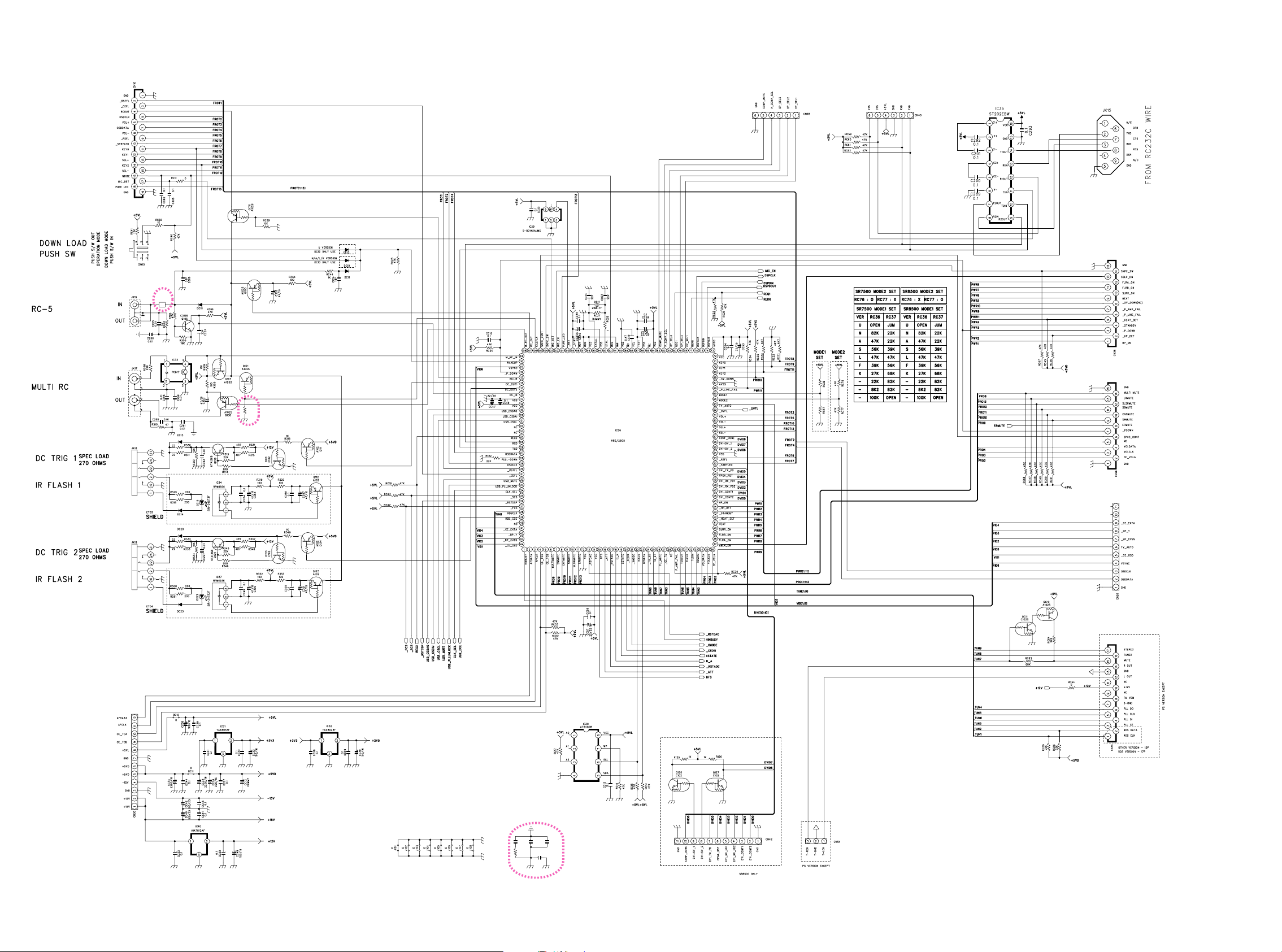
4. SERVICE MODE
4. SERVICE MODE
Microprocessor (IC36), DSP(IC20 )Version and FLD Segment Check Mode.
1. While the power is on, PURE DIRECT, MRAC and 7.1CH
INPUT buttons simultaneously more than 3 seconds.
The FL display shows “SERVICE MODE” for 2 seconds
then shows the model name.
SERVI CE MODE
SR8500
2. Press ENTER button, The software version of the micro-
processor (IC36) is displayed in the format below.
V040805 1U
Year
Month Date Dest.
(Dest. : Destination)
3. Press ENTER button again, The software Serial Number
that is wirtten in the factory is displayed.
Microprocessor (IC36), DSP(IC20 )ƷVersion
ໜ༔ǛᄩᛐƢǔȢȸȉưƢŵ
1.
ǻȃȈƷᩓเǛλǕLJƢŵ
7.1CH IN PUT
“SERVICE MODE”
ᆔӸƕᘙᅆƞǕLJƢŵ
ƷȜǿȳǛӷƴኖ3ᅺˌɥƠLJƢŵ
ƱᘙᅆƕЈLJƢŵƴኖ2ᅺࢸƴೞ
PURE DIRECTŴ MRAC
ᘙᅆӏƼ
SERVI CE MODE
SR8500
2. ENTER
ȳƕഏƷǑƏƴᘙᅆƞǕLJƢŵ
ȜǿȳǛƠLJƢŵȞǤdzȳᲢ
IC36
ᲣƷȐȸǸȧ
V040805 1U
Year
3.
ENTER
Software Serial No.
Month Date Dest.
ȜǿȳǛƠLJƢŵئưƖᡂLjฎLjƷ
ƕᘙᅆƞǕLJƢ
FL
Ŵ
MZXXXXXX XXXXX
4. Press ENTER button again, The software Type Number
is displayed.
SOFT TYPE XX
(XX is displayed in Hex)
5. Press ENTER button again, The Code Group Type
Number is displayed.
CODE TYPEXXXX
(XXXX is displayed in Hex)
6. Press ENTER button again, The left half, right half and
center of the label area in the FLD light on and off each
other.
7. Press ENTER button again, The segments of the character area in the FLD fl ick in checker pattern.
8. Press ENTER button again, All the FL segments turns
off.
9. Press ENTER button again. Every time ENTER button
is pressed, DSP code is indicated in turn from NO.1 to
NO.28.
MZXXXXXX XXXXX
4. ENTER
Soft ware Type
ȜǿȳǛƠLJƢŵȞǤdzȳᲢ
ƕᘙᅆƞǕLJƢŵ
IC36
ᲣƷ
SOFT T YPE XX
(XX: Hex
5. ENTER
ǕLJƢŵ
ȜǿȳǛƠLJƢŵ
Code Group Type
ƕᘙᅆƞ
CODE T YP E X X XX
(XXXX: Hex
6. ENTER
Ўƕʩʝƴໜ༔ǛጮǓᡉƠLJƢŵ
7. ENTER
๒ƠLJƢŵ
8. ENTER
9. ENTER
DSP Code IDƕNO.1
Ƣŵ
ȜǿȳǛƠLJƢŵFLᘙᅆƷӫŴŴɶځᢿ
ȜǿȳǛƠLJƢŵFLƷ
ȜǿȳǛƠLJƢŵFLƕμෞ໊ƠLJƢŵ
ȜǿȳǛƠLJƢŵ
Ɣǒ
Character
ENTER
NO.28
ȜǿȳǛƢࡇƴ
LJưƴᘙᅆƞǕLJ
ᢿЎƕໜ
)
)
CD01 01020101
SIGDev. TYP Ver.No.
No. : DISP CODE ID Dev. : Device ID SIG. : CODE SIG ID
TYP. : CODE TYPE ID Ver. : Version
10. Press ENTER button again to quit this mode.
CD01 01020101
SIGDev. TYP Ver.No.
No. : DISP CODE ID Dev. : Device ID SIG. : CODE SIG ID
TYP. : CODE TYPE ID Ver. : Version
10ENTER
LJƢŵ
9
ȜǿȳǛƠLJƢŵǵȸȓǹȢȸȉƸᚐᨊƞǕ
Page 12

Note: Step4, 5 is to check if CPU software is capable of
DSP code. “Software Type No” is to show what “DSP
Code Group” CPU is capable of. And vice versa.
Step 9 is to manage the 40 codes for DSP.
• When the unit is once turned into Service Mode, the
unit keeps this mode until the main power is turned
off. (Turning into stand-by mode does not make it
quit from Service Mode.) When the unit quits from
Service Mode, Information in the memory is also
cleared and the unit returns to the status when it is
out from the factory.
Product Reset
To reset the back up memory of the unit into the default status, follow the procedure below.
1. Turn of the unit and press SPEAKERS A/B and MULTI
button simultaneously more than 1.5 seconds.
2. After “DEFAULT” is displayed on FLD, power is turned
off once and turned of again, EEPROM is cleared to
the default status, µ-com is reset and the unit returns to
the normal status. (Software Serial Number will not be
cleared.)
Note: When the unit is shipped from the factory, the proce-
dure above must be done to set the unit to initial sta-
Personal notes:
10
Page 13

5. SYSTEM ERROR
ီࠝ౨Јᘙᅆŵ
ီࠝ౨Јᘙᅆŵ
ီࠝ౨Јᘙᅆŵ
ီࠝ౨Јᘙᅆŵ
ီࠝ౨Јᘙᅆŵ
ီࠝ౨Јᘙᅆŵ
ӭီࠝ౨Јᘙᅆŵ
5. SYSTEM ERROR
When the microcomputer detects a trouble, the following information is displayed on the FLD.
• After the error contents indication, Surround Mode is
initialized and returned Factory mode.
• The contents of the ERROR indication are the followings.
1. Trouble in DSP
If communication with DSP is troubled more than 2
seconds.
CHECK DSP ROM
Indication is keep and sound is mute.
2. Trouble in DSP Code
The trouble of DSP Code was found.
CHECK DSP ROM
3. Trouble in EEP-ROM
If data from EEPROM does not match.
CHECK E2P
4. Trouble in EEP-ROM IF
If communication with EEPROM is troubled more than 2
seconds.
ᙌԼϋᢿưƷီࠝႆဃƴϼྸŴᘙᅆǛᘍƍLJƢŵɼƴӲ
Device
ƱƷᡫီࠝǛ౨ЈƠLJƢŵ
ERROR
ƷཞƴǓLJƢŵ
ERROR
1. DSP
DSP
ᘙᅆࢸŴ
ᘙᅆƷϋܾƸɦᚡưƢŵ
ီࠝ౨Јᘙᅆŵ
ƱƷᡫɥƷɧφӳǛኖ ᅺ౨ЈƠƨŵ
SurroundMode
ƸИ҄ƞǕئЈᒵ
CHECK DSP ROM
ᘙᅆཞƸƦƷLJLJư᪦٣Ƹ /WVG ཞ
2. DSP Code
DSPCode
ီࠝ౨Јᘙᅆŵ
ƷီࠝǛ౨ЈƠƨŵ
CHECK DSP ROM
3. EEP-ROM
EEPROMData
ီࠝ౨Јᘙᅆŵ
ƷɧૢӳǛ౨ЈƠƨŵ
CHECK E2P
4. EEP-ROM IF
EEPROM
ီࠝ౨Јᘙᅆŵ
ƱƷᡫɧφӳƕኖ ᅺˌɥဃơƨŵ
CHECK E2P I F
5. Trouble in RS-232C
If communication of Panja with RS232C is troubled more
than 2 seconds.
CHECK 2 32C
6. Trouble in 5V Supply
If 5V supply to DATA DIR is troubled.
CHECK POW5
7. Trouble in Protection
CPU turns off the speaker output.
PROTECT
CHECK E2P I F
5. RS-232C
Panja
ɥ౨ЈƠƨŵ
ီࠝ౨Јᘙᅆŵ
ᡫƴRSCƱƷᡫɧφӳǛኖ ᅺˌ
CHECK 2 32C
6. 5V
ီࠝ౨Јᘙᅆŵ
DATADIR
ƷီࠝǛ౨ЈƠƨŵ
CHECK POW5
7. Protection
Speaker
ӭီࠝ౨Јᘙᅆŵ
ƔǒǛЈщǛഥNJLJƢŵ
PROTECT
11
Page 14
6. UPDATE FIRMWARE
ƷǢȃȗȇȸȈ૾ඥ
6. UPDATE FIRMWARE
Software for CPU and DSP can be updated.
Have update application software. (“UpgradeDSP.exe” and
“H8Download.exe”)
There are two mode of download, regarding to the target of
software as bellow.
Mode 1: Update DSP’s software to Flash-ROM.
This mode is to update the software for DSP.
The target devise is Flash-ROM (IC20) on CUP11762Z
(DSP PCB).
The Unit needs to be set update condition, by three front
keys.
Mode 2: Update CPU’s software to internal Flash-ROM.
This mode is to update the software for DSP.
The target devise is internal fl ash ROM of CPU (IC36) on
CUP11762Z (DSP PCB).
The Unit needs to be set to writing condition, by pushing
internal switch from back-panel.
The following items are required for updating.
RS232C Dsub-9 pin cable (female to female/Straight type)
Windows PC (98, NT, ME, 2000) with RS-232C port.
Update software to CPU.
Update software to DSP.
Use RS232C Dsub-9 pin cable (female to female/Straight
type) to connect PC and the unit.
COM port on PC needs to be set by dialog box for each program. COM port can be set from COM1 to COM5.
CPU ƓǑƼ DSP ǽȕȈǦǧǢƷǢȃȗȇȸȈǛᘍƍLJƢ
ǽȕȈǦǧǢƷǢȃȗȇȸȈƴƸUpgradeDSP.exe Ʊ
H8Download.exe ƕ࣏ᙲưƢŵ
ǢȃȗȇȸȈƴƸഏƷʚƭƷȢȸȉƕƋǓLJƢŵ
Mode 1:DSP ဇ Flash-ROM ƷǢȃȗȇȸȈ
ƜƷȢȸȉƸ
ȉưƢŵ
DSP ƷǽȕȈǦǧǢǛǢȃȗȇȸȈƢǔȢȸ
CUP11762(DSP PCB) ƷؕெɥƴƋǔ Flash-ROM (IC20)
ƷǽȕȈǦǧǢǛǢȃȗȇȸȈƠLJƢŵ
ஜೞ
[PS7500 / PS8500] ƷȕȭȳȈȑȍȫƴƋǔ 3 ƭƷȜ
ǿȳǛƠƯǢȃȗȇȸȈȢȸȉƴƠLJƢŵ
Mode 2:CPU Ʒϋᢿ Flash-ROM ƷǢȃȗȇȸȈ
ƜƷȢȸȉƸ
ȉưƢŵ
CPU ƷǽȕȈǦǧǢǛǢȃȗȇȸȈƢǔȢȸ
CUP11762(DSP PCB) ƷؕெɥƴƋǔ CPU(IC36) Ʒϋᢿ
Flash-ROM ƷǽȕȈǦǧǢǛǢȃȗȇȸȈƠLJƢŵ
[PS7500 / PS8500]
ஜೞ
ƠƯǢȃȗȇȸȈȢȸȉƴƠLJƢŵ
ǢȃȗȇȸȈƴƸɦᚡƷೞ֥ƕ࣏ᙲưƢŵ
ƷȪǢȑȍȫƔǒϋᢿǹǤȃȁǛ
( ࣏ᙲೞ֥ )
RS-232C ǹȈȬȸȈDZȸȖȫ (9Pin ȡǹ -9Pin ȡǹ )
Windows PC Serial Port ˄Ɩ (OS: 98,NT,ME,2000)
CPU ဇǢȃȗȇȸȈǽȕȈǦǧǢ
DSP ဇǢȃȗȇȸȈǽȕȈǦǧǢ
RS-232C DZȸȖȫưஜೞƱዓƢǔ PC Ʒ COM ȝȸȈဪӭ
ǛᚨܭƠƯƘƩƞƍŵ
COM ȝȸȈဪӭƸ COM1 Ɣǒ COM5 LJưᚨܭưƖLJƢŵ
Download Firmware for DSP (Mode 1)
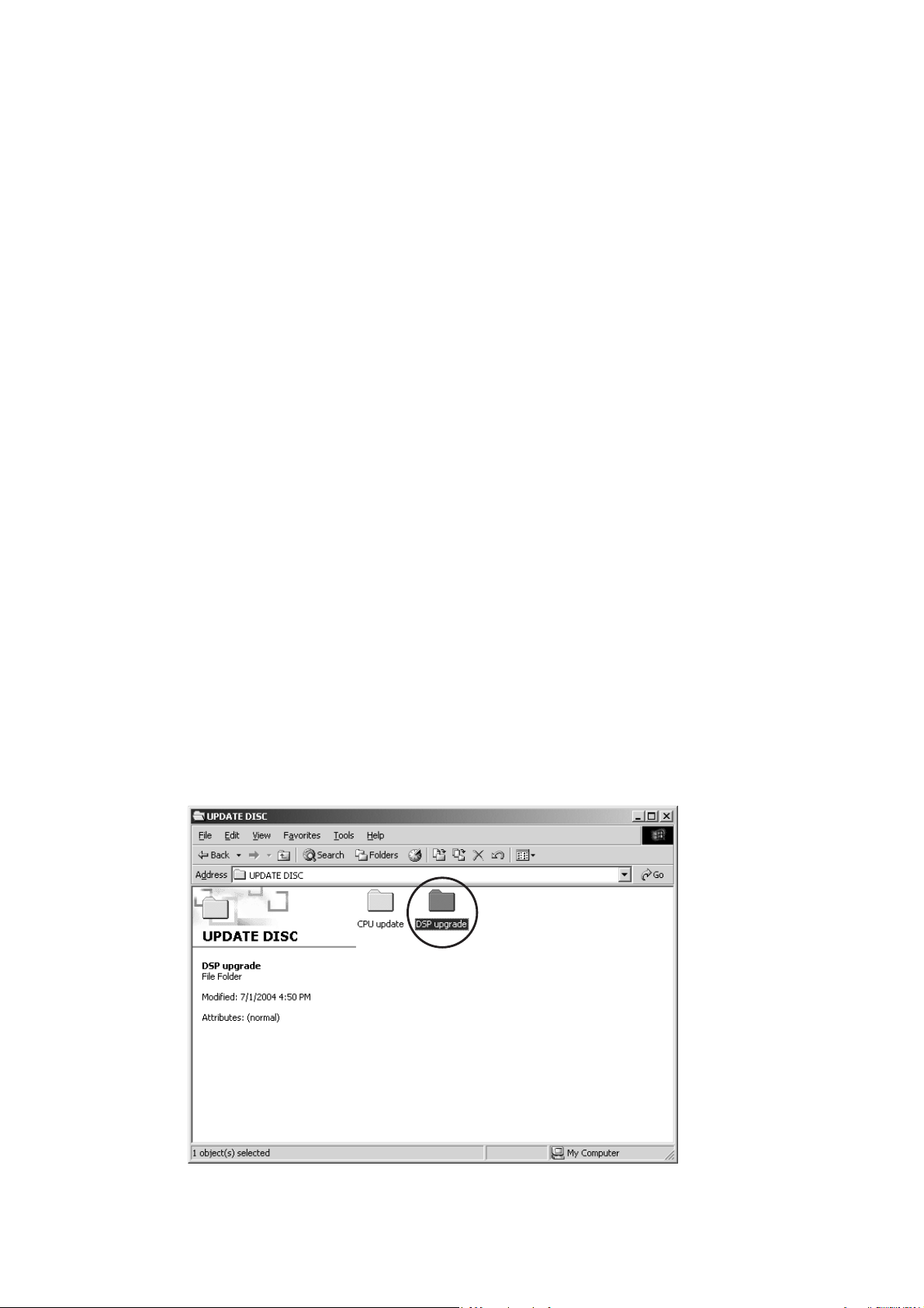
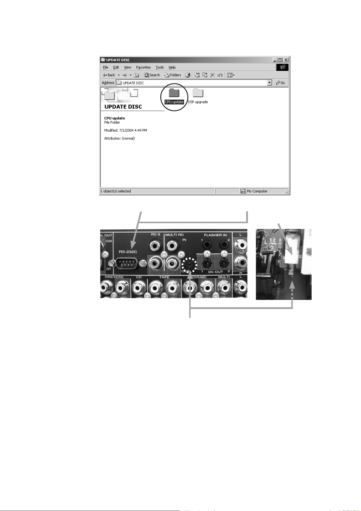
1. Put the “DSP upgrade” folder into anywhere on your PC’
s hard disc.
2. Connect PC and the unit with the RS-232C cable.
DSP
ƷǢȃȗȇȸȈ૾ඥ (Mode 1)
1. "DSP upgrade" ȕǩȫȀǛ PC ƷȏȸȉȇǣǹǯƴdzȔȸ
ƠLJƢŵ
2. ஜೞƱ PC Ǜ RS-232C ưዓƠLJƢŵ
3. Turn on the unit.
3. ஜೞƷᩓเǛλǕLJƢŵ
12
Page 15
4. [SR7500 / SR8500]
දᚡ
Press ENTER, SURROUND MODE and T-MODE
buttons simultaneously more than 5 seconds to turn the
unit into Loading Mode.
[PS7500 / PS8500]
Press ENTER, SURROUND MODE and SLEEP buttons
simultaneously more than 5 seconds to turn the unit into
Loading Mode.
5. “LOADING MODE” will be shown on FLD.
4. ENTER, SURROUND MODE, SLEEP
ƴ
5 ᅺˌɥƠዓƚƯ Loading Mode ƴƠLJƢŵ [PS7500
Ʒ 3 ƭƷȜǿȳǛӷ
/ PS8500]
ȇǣǹȗȬǤƴ "LOADING MODE" ƱᘙᅆƞǕLJƢŵ
5. FL
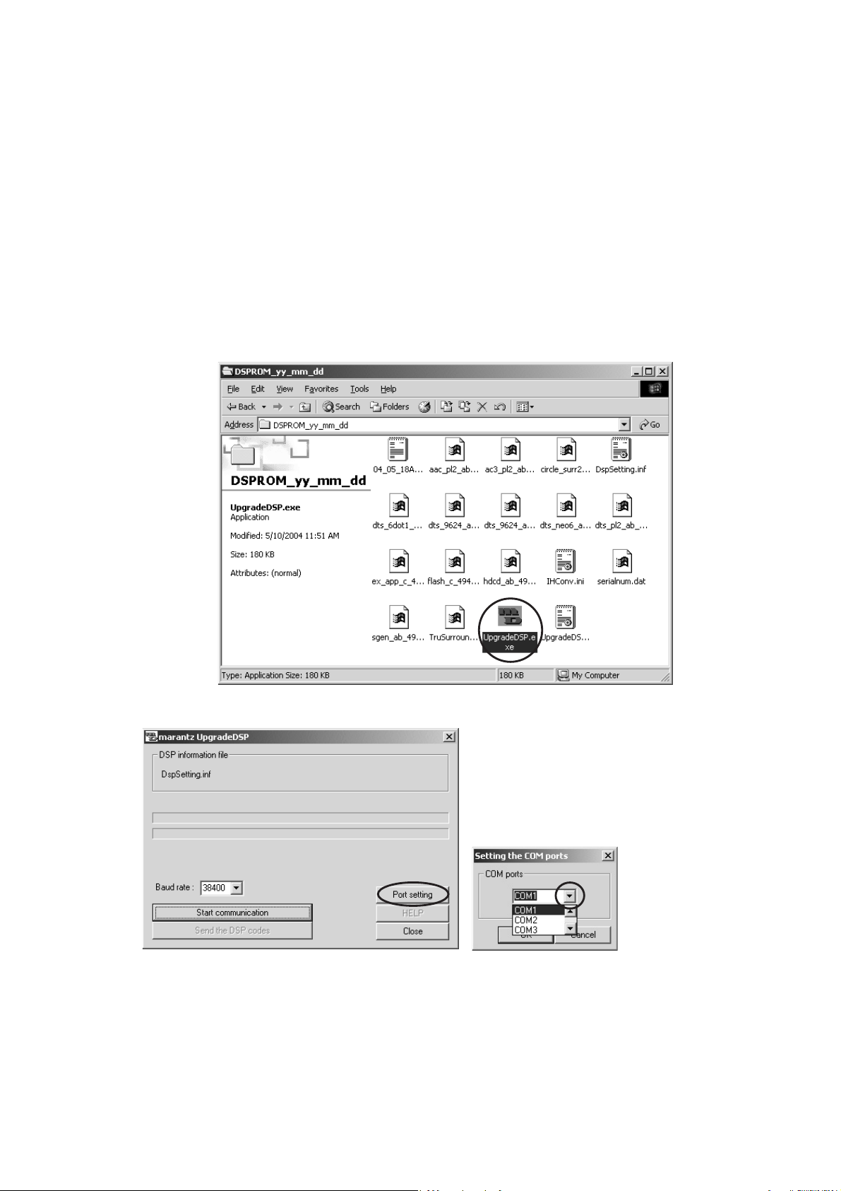
6. Launch “UpgradeDSP.exe” on PC.
Note: yy_mm_dd is release date of software.
6. PC Ɣǒ "UpgradeDSP.exe" ǛȀȖȫǯȪȃǯƠƯឪѣƠLJ
Ƣŵ
දᚡ : ȕǡǤȫӸƷ yy_mm_dd ƸǽȕȈǦǧǢƷႆᘍଐǛ
ƋǒǘƠLJƢŵ
7. Click Port setting, and select the COM Port No.
7. Port setting ǛǯȪȃǯƠŴCOM ȝȸȈဪӭǛᢠ৸ƠLJƢŵ
13
Page 16
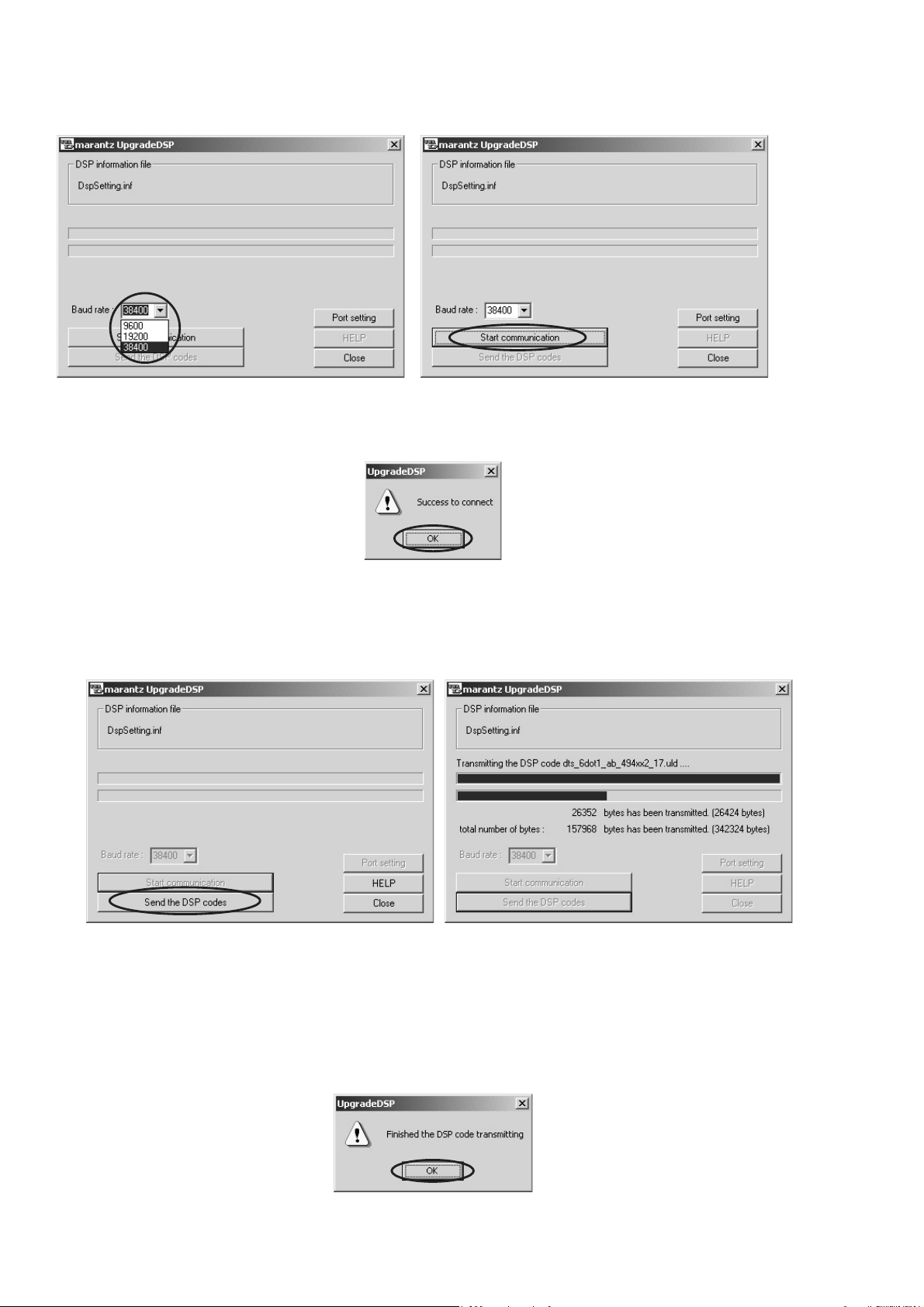
8. Set the Baud rate to 38400 then click Start communi-
cation button.
8. Baud rate Ǜ 38400 ƴᚨܭƠŴStart communication Ǜǯ
ȪȃǯƠLJƢŵ
9. If the connection is made successfully, a dialog box saying “Success to connect” appears and “CONNECTED” is
displayed on FLD.
10. Click Send the DSP codes button on the dialog box.
Progress status of updating will be shown on PC and
LOADING is displayed on FLD.
9. ᡫዓƴыƢǔƱɦᚡƷȀǤǢȭǰȜȃǯǹƕᘙᅆƞ
ǕŴ
FL ȇǣǹȗȬǤƴƸ "CONNECTED" ƕᘙᅆƞǕLJƢŵ
10. Send the DSP codes ǛǯȪȃǯƠLJƢŵǢȃȗȇȸ
ȈƷǹȆȸǿǹȐȸƕᘙᅆƞǕŴ
FL ȇǣǹȗȬǤƴƸ
"LOADING" ƕᘙᅆƞǕLJƢŵ
11. If updating is completed successfully, “COMPLETED” is
displayed on FLD. And a dialog box saying “Finished the
DSP code transmitting” appears.
12. Click OK and then Application is closed automatically.
13. Turn off the unit.
14
11. ǢȃȗȇȸȈƕыƢǔƱFL ȇǣǹȗȬǤƴ
"COMPLETED" ƱᘙᅆƞǕLJƢŵӷƴ "Finished the
DSP code transmitting" ƷȀǤǢȭǰȜȃǯǹƕᘙᅆƞǕ
LJƢŵ
12. OK ǛǯȪȃǯƢǔƱᐯѣႎƴǢȗȪDZȸǷȧȳƕơLJ
Ƣŵ
13. ஜೞƷᩓเǛЏǓLJƢŵ
Page 17
Download Firmware for CPU (Mode 2)
ƷǢȃȗȇȸȈ૾ඥ
දᚡ
1. Put the “CPU update” folder into anywhere on your PC’s
hard disc.
ƷǢȃȗȇȸȈ૾ඥ (Mode 2)
CPU
1. "CPU update" ȕǩȫȀǛ PC ƷȏȸȉȇǣǹǯƴdzȔȸƠ
LJƢŵ
2. Connect PC and the unit with the RS-232C cable.
Hole of rear panel
ȪǢȑȍȫƴƋǔᆭ
3. Insert a thin rot to the hole and push the switch (SW10)
inside to turn on the switch.
4. Turn on the power of the unit.
Note: When the unit is into boot mode, stand-by LED is
not lights up.
2. ஜೞƱ PC Ǜ RS-232C ưዓƠLJƢŵ
SW10
3. ኬƍొǛƍஜೞƷȪǢȑȍȫƴƋǔᆭƔǒǹǤȃȁ
(SW10) ǛƠLJƢŵ
4. ஜೞƷᩓเǛλǕLJƢŵ
දᚡ : ஜೞƸȖȸȈȢȸȉƴƳǓŴStand-by LED Ƹໜ໊Ơ
LJƤǜŵ
15
Page 18
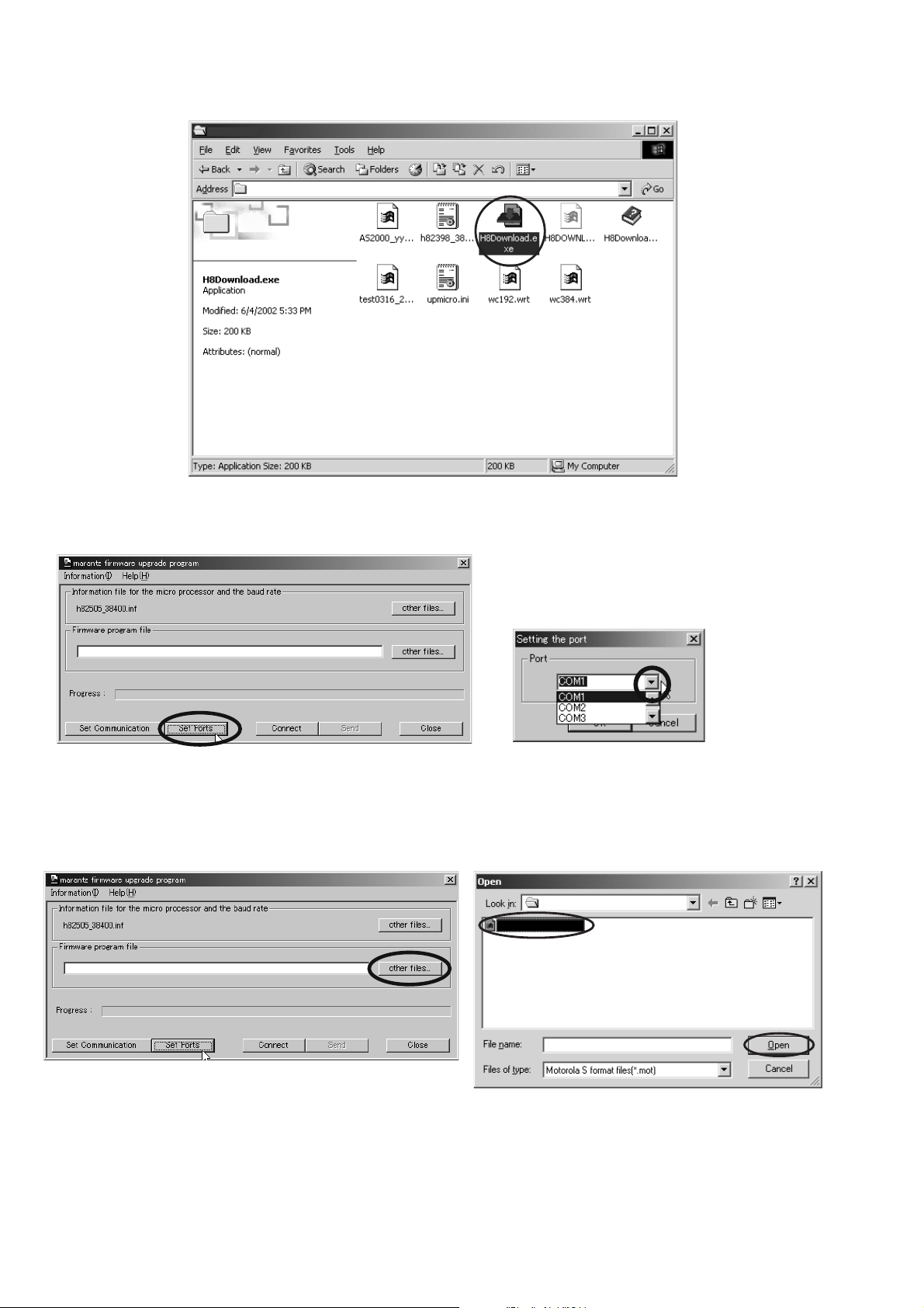
5. Launch "H8Download.exe" on PC.
H8FW2505
H8FW2505
H8FW2505
5. PC Ɣǒ "H8Download.exe" ǛȀȖȫǯȪȃǯƠƯឪѣƠLJ
Ƣŵ
6. Click Set Ports, and select the COM Port No.
7. Click other fi les... button in the dialog box to specify the
fi le (SR8500_yymmdd.mot) to be uploading. yymmdd in
fi lename is release date of software.
6. Set Ports ǛǯȪȃǯƠŴCOM ȝȸȈဪӭǛᢠ৸ƠLJƢŵ
7. other fi les… ǛǯȪȃǯƠƯŴǢȃȗȇȸȈȕǡǤȫ
(SR8500_yymmdd.mot) Ǜᢠ৸ƠƖLJƢŵ
H8FW2505
SR8500_yymmdd.mot
16
SR8500_yymmdd.mot
Page 19
8. Click Connect button. If the connection with the H8 µ-P
is successfully made, a dialogue box saying "Success to
the H8 micro processor connection" appears. (If the connection fails, error message will appear.)
8. Connect ǛǯȪȃǯƠLJƢŵH8 u-P ƱᡫዓƴыƢǔ
Ʊ
"Success to the H8 micro processor connection" ƷȀǤ
ǢȭǰƕᘙᅆƞǕLJƢŵ ᡫƴڂƢǔƱǨȩȸȡȃǻȸ
ǸƕᘙᅆƞǕLJƢŵ
9. Click Send button to start update.
h82505_38400.inf
10. If the fi rmware is updated successfully, a dialog box saying "Finished the fi rmware program sending” appears.
9. Send ǛǯȪȃǯƠǢȃȗȇȸȈǛڼƠLJƢŵ
10. ǽȕȈǦǧǢƷǢȃȗȇȸȈƕыƢǔƱŴ"Finished the
fi rmware program sending" ƷȀǤǢȭǰȜȃǯǹƕᘙᅆ
ƞǕLJƢŵ
17
Page 20

11. Click Close button to close the application.
ȐȸǸȧȳƷᄩᛐ
h82505_38400.inf
11. Close ǛǯȪȃǯƠƯǢȗȪDZȸǷȧȳǛơLJƢŵ
12. Disconnect Mains power cord.
13. Turn off the internal switch that has been turned on at
step 3.
14. Turn on the unit.
Firmware Version Check
To check the versions of the fi rmware, see "Microprocessor
(CPU), DSP Version and FLD Segment Check Mode" in
"SERVICE MODE" section.
12. ஜೞƷᩓเǛЏǓLJƢŵ
13. 3 ƷǹǤȃȁᲢSW10ᲣǛƠƯȖȸȈȢȸȉǛᚐᨊƠ
LJƢŵ
14. ᩓเǛλǕLJƢŵ
ȐȸǸȧȳƷᄩᛐ
ǽȕȈǦǧǢƷȐȸǸȧȳǛᄩᛐƠLJƢŵᄩᛐ૾ඥƸ
"SERVICE MODE" ϋƷ"Microprocessor (CPU), DSP
Version and FLD Segment Check Mode"ǛӋༀƠƯƘƩƞƍŵ
18
Page 21
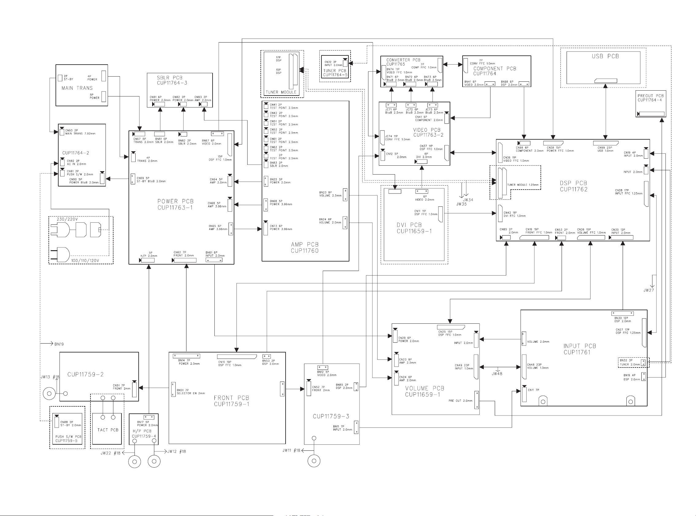
7. WIRING DIAGRAM
SR7500/SR8500 Only PS7500/PS8500 Only
STANDBY PCB
CN66
CN65
CN71
AUX1
CN12 6P
POWER 2.0mm
CN71
CN21
BN13
CN42
AUX1
CN34 15P/P17
CN46 4P
BN22 15P
VOLUME 2.0mm
SELECTOR PCB
CN63
BN52 7P
AUX1 2mm
AUX1 PCB
SR8500/PS8500 Only
CN47 6P
CN22 15P
BN47 6P
AUX1 2.0mm
A, F, K, L, N only
U only
19 20
Page 22
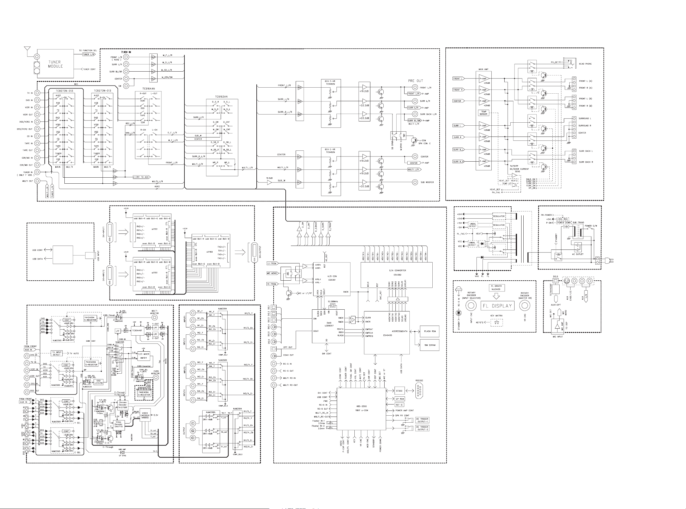
8. BLOCK DIAGRAM
SR7500/SR8500 only
USB MODULE
SR8500/PS8500 only
DVI PART
SR8500/PS8500 only
2221
Page 23
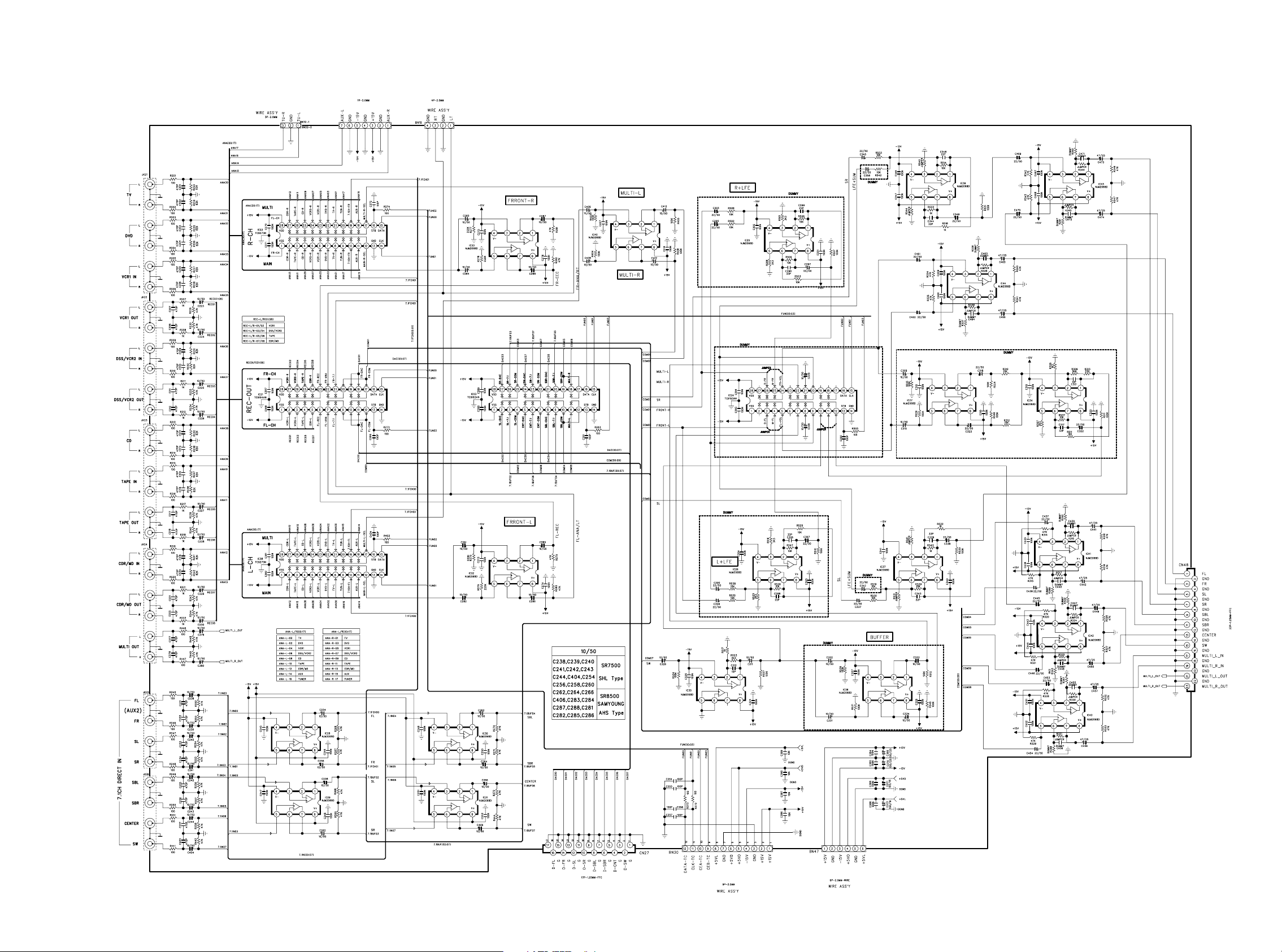
9. SCHEMATIC DIAGRAM
INPUT PCB
FROM TUNER PCB (F VERSION)
FROM DSP PCB (OTHER VERSION)
FROM AUX1 PCB FROM DSP PCB
CN11
FROM DSP PCB
FROM DSP PCB
FROM VOLUME PCB
23 24
FROM VOLUME PCB
Page 24
TO FRONT PCB
DSP PCB - 1/2
L102
HM102T
TO COMPONENT PCB
TO POWER PCBTO VOLUME PCBTO VIDEO PCB
R380
10k
TO TUNER MODULE
TO INPUT PCB
C325
C323
C322
0.1
0.1
0.1
R360
C324
10
0.1
TO INPUT PCBTO DVI PCB
2625
Page 25

DSP PCB - 2/2
TO AUX1 PCB
TO USB PCB
TO INPUT PCB
TO FRONT PCBTO INPUT PCB
27 28
Page 26
FROM INPUT PCB
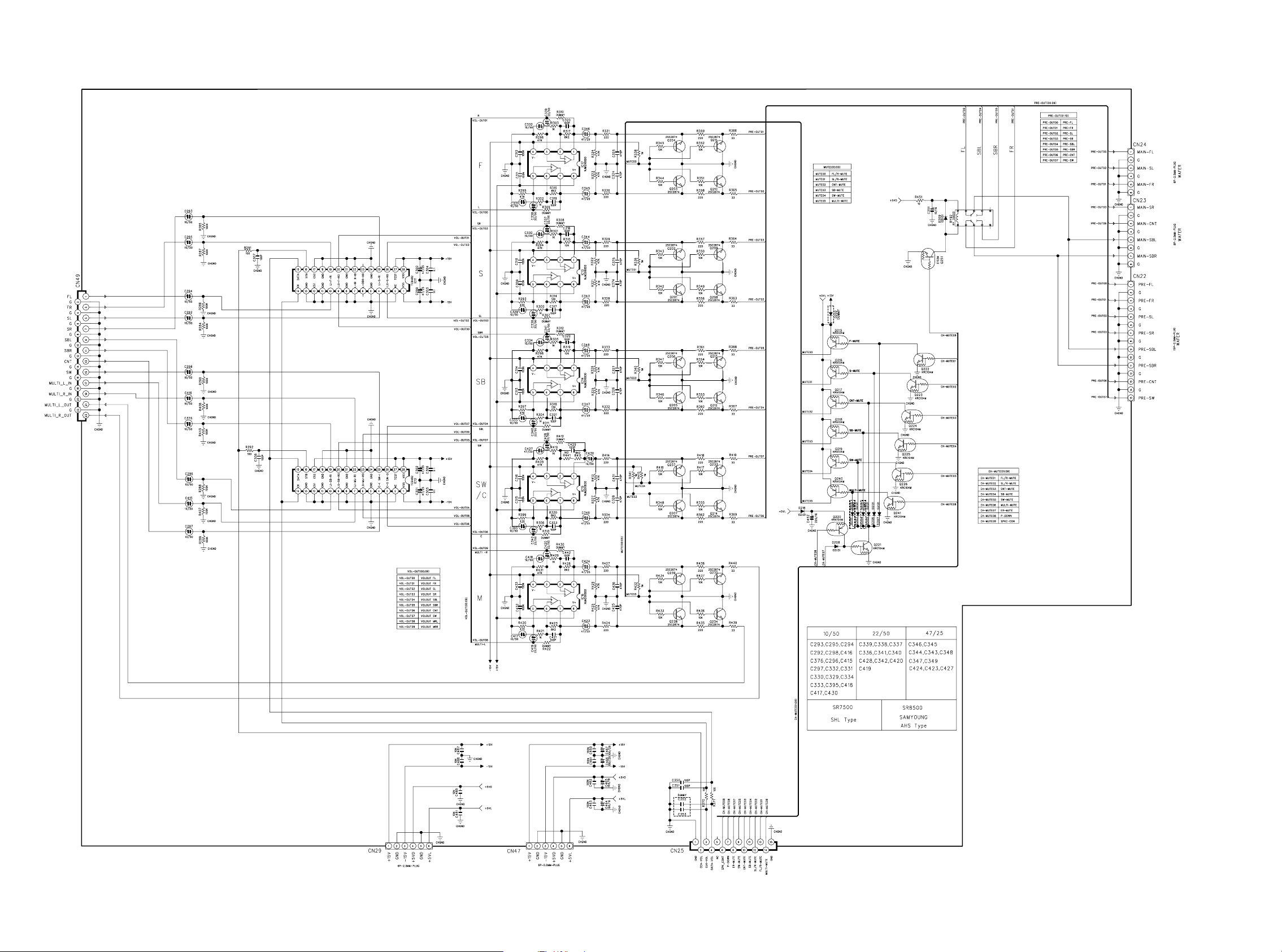
VOLUME PCB
FROM PREOUT PCB FROM AMP PCB FROM AMP PCB
TO POWER PCB
FROM INPUT PCB
FROM DSP PCB
3029
Page 27
AMP PCB
CN82
31 32
Page 28
VIDEO PCB
TO DSP PCB
TO
COMPONENT
PCB
FROM AUX1 PCB
TO CONVERTER
PCB
TO CONVERTER
PCB
SW-C-IN
TO CONVERTER PCB
TO CONVERTER PCB
TO
POWER PCB
3433
Page 29
COMPONENT PCB
STANDBY
STANDBY PCB
TO POWER PCB
CN71
FROM CONVERTER PCB
FROM DSP PCB (2/2)
FROM VIDEO PCB
PRE OUT PCB
FROM MAIN TRANS
SBLR PCB
TO POWER PCBTO AMP PCB
TUNER PCB
FROM INPUT PCB
PS7500/PS8500 Only
FROM VOLUME PCB
35 36
Page 30
VIDEO CONVERTER PCB
TO VIDEO PCB
TO VIDEO PCB
TO VIDEO PCB
TO VIDEO PCB
TO COMPONENT PCB
3837
Page 31

JK11
DATA2-
DATA2+
GND
DATA4-
DATA4+
DDC_CLK
DDC_DATA
NC
DATA1-
DATA1+
GND
DATA3-
DATA3+
+5V
DVI-INPUT1
GND
HPD
DATA0-
DATA0+
GND
DATA5-
DATA5+
GND
CLK+
CLK-
DVI PCB
1
2
3
4
5
DDC_CLK_1
6
DDC_DATA_1
7
8
9
10
11
12
13
+5V_1
14
15
HPD_1
16
17
18
19
20
21
22
23
24
GND
GND
C111 0.1u
GND
RX1-DATA
+3.3VDI
L101 10uH
C109 0.1u
GND GND
C112 0.1u
GND
C110 47u/16
0.1uC113
GND
C108 0.1u
R106 390
R107 10K
GNDGND
GNDGNDGNDGNDGNDGND
R108 10K
GND
C107
47u/16
76
OGND
77
QO23
78
OVCC
79
AGND
80
RX2+
81
RX2-
82
AVCC
83
AGND
84
AVCC
85
RX1+
86
RX1-
87
AGND
88
AVCC
89
AGND
90
RX0+
91
RX0-
92
AGND
93
RXC+
94
RXC-
95
AVCC
96
EXT_RES
97
PVCC
98
PGND
99
MODE
100
SCL
HS_DJTR2PD3SDA/ST4PIXS5GND6VCC7I2C_MODE#(STAG_OUT#)
1
R101 0
GND
R102 10K
C106
0.1u
GND
67
68
69
VCC
GND
QO1670QO1771QO1872QO1973QO2074QO2175QO22
IC11
SiI1161
EVEN 8Bit B
SCDT9PDO#10QE011QE112QE213QE314QE415QE516QE617QE718OVCC19OGND20QE821QE922QE1023QE1124QE1225QE13
8
GND GND
0
10K
R104
R105
R103 10K
GND
RX_PD_1
8642
22
RN11
13 75
C101 0.1u
B[0]
B[1]
B[2]
B[3]
CN11
11
DVI_CONT2
10
DVI_CONT1
9
DVI_RX_PD2
8
DVI_RX_PD1
7
GND
FPGA_RST
6
DVI_TX_PD
5
DVI_+5V_2
4
DVI_+5V_1
3
2
GND
1
TO DSP PCB
R185
R184
100
C105
0.1u
GNDGND
GND
51
57
58
59
61
QO252QO353QO454QO555QO656QO7
QO860QO9
QO1062QO1163QO1264QO1365QO1466QO15
OVCC
OGND
8642
13 75
B[5]
B[6]
B[7]
B[4]
ODD 8Bit BODD 8Bit GODD 8Bit R
EVEN 8Bit G
22
RN12
EVEN 8Bit R
GND
SIL1161-1
QO1
QO0
HSYNC
VSYNC
DE
OGND
ODCK
OVCC
CTL3
CTL2
CTL1
GND
VCC
QE23
QE22
QE21
QE20
QE19
QE18
QE17
QE16
OVCC
OGND
QE15
QE14
C102 0.1u
C104 0.1u
GND
50
RN18
49
48
47
46
45
44
43
42
41
40
39
38
37
36
35
34
33
32
31
30
29
28
27
26
GND GND GND
GND
22
1375
13
75
RN16 22
1375
13
75
RN15
22
0.1u
C103
RN14
22
13
75
1375
RN13
22
8642
RN17
22
8642
8642
8642
8642
8642
C[6]
C[5]
C[4]
C[3]
C[2]
C[1]
C[0]
R[7]
R[6]
R[5]
R[4]
R[3]
R[2]
R[1]
R[0]
G[7]
G[6]
G[5]
G[4]
G[3]
G[2]
G[1]
G[0]
RX_PD_2
RX_PD_1
DDC_CLK_1
DDC_CLK_2
DDC_DATA_2
DDC_DATA_1
+5V_2
+5V_1
HPD_2
HPD_1
DOC_CLK
DOC_DATA
+5V
HPD
GND
IC18
74VHC08TTR
RY11
678910
RY12
678910
8 9 10 11 12 13 14
GND
12345
GND
12345
GND
D101
D102
Q101
1N4148
1N4148
A102S
1234567
+3.3VDI
+5VV
C199
0.1u
GND
RY13
RY14
12345
678910
DOC_DATA DOC_CLK
GND
12345
678910
HPD +5V
GND
Q103
D103
A102S
D104
1N4148
1N4148
+5VV
100
JK12
DATA2-
DATA2+
GND
DATA4-
DATA4+
DDC_CLK
DDC_DATA
NC
DATA1-
DATA1+
GND
DATA3-
DATA3+
+5V
DVI-INPUT2
GND
HPD
DATA0-
DATA0+
GND
DATA5-
DATA5+
GND
CLK+
CLK-
1
2
3
4
5
6
7
8
9
10
11
12
13
14
15
16
17
18
19
20
21
22
23
24
GND
DDC_CLK_2
DDC_DATA_2
+5V_2
HPD_2
GND
C131 0.1u
GND
+3.3VDI
10uH
L121
C129 0.1u
GND
C132 0.1u
GND
GND
0.1u
C133
GND
47u/16
C130
C128 0.1u
GND
R126 390
R127 10K
GND
GND
GND
GND
GND
GND
GND
10K
R128
GND
100
C127
76
77
78
79
80
81
82
83
84
85
86
87
88
89
90
91
92
93
94
95
96
97
98
99
47u/16
OGND
QO23
OVCC
AGND
RX2+
RX2AVCC
AGND
AVCC
RX1+
RX1AGND
AVCC
AGND
RX0+
RX0AGND
RXC+
RXCAVCC
EXT_RES
PVCC
PGND
MODE
SCL
GND
75
QO22
HS_DJTR
1
2
R121 0
R122 10K
RX_PD_2
GND
67
68
69
71
GND
QO1670QO17
QO1872QO1973QO2074QO21
VCC7I2C_MODE#(STAG_OUT#)
SCDT9PDO#10QE011QE1
PD3SDA/ST4PIXS5GND
6
8
GND
10K
R124
R125
R123 10K
0.1u
22
RN21
C121
GND
C126
0.1u
GND
65
VCC
QO1466QO15
ODD 8Bit G
IC12
SiI1161
EVEN 8Bit B
QE213QE314QE415QE516QE617QE718OVCC19OGND
12
0
8642
13 75
B[3]
B[2]
B[1]
B[0]
Q102
C102S
GND
64
DIO965DIO8
ODD 8Bit G
IC16
B[3]
B[4]
B[5]
GND
C188 0.1u
GNDGND
56
57
58
VCC
GND
DIO1559DIO1460DIO1361DIO1262DIO1163DIO10
ODD 8Bit R
GND
GND
R181 10K
C182 0.1u
GND
0.1u
C180
R182 0
GND
B[0]
B[1]
B[2]
GND
+3.3VDI
C125
0.1u
GND
GND
57
58
51
52
56
59
61
QO353QO454QO555QO6
QO2
QO7
QO860QO9
QO1062QO1163QO1264QO13
OVCC
OGND
GND
8642
13 75
B[7]
B[6]
B[5]
B[4]
ODD 8Bit BODD 8Bit R
EVEN 8Bit G
QE821QE922QE1023QE1124QE1225QE13
20
22
RN22
EVEN 8Bit R
GND
SIL1161-2
QO1
QO0
HSYNC
VSYNC
DE
OGND
ODCK
OVCC
CTL3
CTL2
CTL1
GND
VCC
QE23
QE22
QE21
QE20
QE19
QE18
QE17
QE16
OVCC
OGND
QE15
QE14
0.1u
C122
0.1u
C124
GND
50
RN28
49
48
47
46
45
44
43
42
41
40
39
38
37
36
35
34
33
32
31
30
29
28
27
26
GND
GND
GND
GND
22
1
3
75
13
75
RN26 22
1375
1375
RN25
22
0.1u
C123
RN24
22
1375
13
75
RN23
22
8642
RN27
22
8642
8642
8642
8642
8642
C[6]
C[5]
C[4]
C[3]
C[2]
C[1]
C[0]
R[7]
R[6]
R[5]
R[4]
R[3]
R[2]
R[1]
R[0]
G[7]
G[6]
G[5]
G[4]
G[3]
G[2]
G[1]
G[0]
L182
10uH
0.1u
C191
C190
47u/16
GND
GND
C194
76
HSYNC
77
VSYNC
78
DE
79
GND
80
GNDGND GND
IDCK
C192
81
IVCC
0.1u
82
CTL3
83
CTL2
84
CTL1
85
PVCC2
86
C193
0.1u
0.1u
PGND2
87
RSVD
88
VCC
89
GND
90
DIE23
91
DIE22
92
DIE21
93
DIE20
94
DIE19
95
DIE18
96
DIE17
97
DIE16
98
IVCC
99
DIE15
EVEN 8Bit G
100
DIE14
G[6]
G[7]
C[6]
C[5]
C[4]
C[3]
GND
C[2]
C[1]
C[0]
GND
R[7]
R[6]
R[5]
R[4]
R[3]
R[2]
R[1]
R[0]
GND
GND
C189 0.1u
66
67
68
NCC
GND
DIO769DIO670DIO571DIO472DIO373DIO274DIO175DIO0
ODD 8Bit B
EVEN 8Bit R
DIE132DIE123DIE114DIE105DIE96DIE87GND8VCC9DIE710DIE611DIE512DIE413DIE314DIE215DIE116DIE017IVCC18PVCC119PGND120RSVD21RSVD22RSVD23RSVD24EDGE25PIXS
1
G[4]
G[5]
SiI160
EVEN 8Bit B
GND GND
GND
C181 0.1u
G[0]
G[1]
G[2]
G[3]
B[6]
B[7]
51
DIO2052DIO1953DIO1854DIO1755DIO16
DIO21
DIO22
DIO23
AGND
TX2+
TX2AVCC
TX1+
TX1AGND
TX0+
TX0AVCC
AGND
AVCC
TXC+
TXCAGND
EXT_SWING
GND
VCC
RSVD
RSVD
RSVD
C187
GNDGND
PD
Q104
C102S
GND
+3.3VDI
L181
10uH
0.1u
C186
47u/16
50
49
48
47
46
45
44
43
42
41
40
39
38
37
36
35
34
33
32
31
30
29
28
27
26
C184 0.1u
R183 510
GND
GND GND GND GND
C183 0.1u
C185
0.1u
GND
GND
GND
GND
JK13
1
DATA2-
2
DATA2+
3
GND
4
DATA4-
5
DATA4+
6
DDC_CLK
7
DDC_DATA
8
NC
9
DATA1-
10
DATA1+
11
GND
12
DATA3-
13
DATA3+
14
+5V
15
GND
16
HPD
17
DATA0-
18
DATA0+
19
GND
20
DATA5-
21
DATA5+
22
GND
23
CLK+
24
CLK-
DVI-OUTPUT
+3.3VDI +5VV
IC17
KIA278R33
1
2
IN
OUT
GND
CTL
3
C198
4
10k
0.1u
C197
47/16
GND
R191
C196
0.1u
C195
47/16
GNDGNDGNDGND
12345
BN13
-15V
GND
+15V
+5VV
TO VIDEO PCB
6
GND
+5VL
+5VL
FROM POWER PCB
GND GNDGND GND
CN12
6
GND
12345
-15V
GND
+15V
+5VV
39 40
Page 32

SELECTOR PCB
U VERSION ONLY
FRONT PCB
FROM FRONT PCB
FROM SELECTER PCB
FROM POWER PCB
FROM DSP PCB
FROM AUX1 PCB
AUX1 PCB
FROM FRONT PCB
TO DSP PCB
AUX1
FROM VIDEO PCB
H/P
PUSH S/W
POWER ON/OFF
H/P PCB
A, K, L, F, N VERSION ONLY
PUSH PCB
TO DSP PCB
FROM POWER PCB
PCB
STANDBY
FROM
4241
Page 33

POWER PCB
to
STANDBY
PCB
43 44
Page 34

10. PARTS LOCATION
INPUT PCB
IC38
IC33
IC21
IC32
IC22
IC30IC28
IC31IC29
IC40
IC23
IC25
IC24
IC26 IC37
IC35
IC36
IC39
IC34IC27
IC43
IC42
IC41
IC45
IC44
4645
Page 35

Q719 Q721
Q723
Q707
Q715 Q713
Q709
Q711
Q717
Q620 Q622 Q619 Q621 Q520 Q522 Q519 Q521 Q420 Q422 Q419 Q421
Q608
Q616 Q614
Q624 Q623 Q524 Q523 Q424 Q423
Q610
Q612
Q618
Q607
Q615 Q613
Q609
Q611
Q617
Q508
Q516 Q514
Q510
Q512
Q518
Q507
Q515 Q513
Q509
Q511
Q517
Q408
Q416 Q414
Q410
Q412
Q418
Q407
Q415 Q413
Q409
Q411
IC81
Q417
AMP PCB
Q703 Q705
IC71 IC61 IC51 IC41
Q604 Q606
Q603 Q605
Q504 Q506
Q503 Q505
Q404 Q406
Q403 Q405
Q801 Q803 Q804
PREOUT PCB
47 48
Page 36

IC18
IC19
IC15
Q100
IC17
IC14
Q106
Q104
Q119
Q118Q101
Q112
Q110
IC16
VIDEO CONVERTER PCB A
Q113
Q108
IC12
Q114
Q115
Q116
Q117
IC11
Q120
Q106 Q105
Q108
Q109
Q122
DSP PCB A
IC11
IC12
IC35
Q121
Q107
IC33
Q110 Q111
IC34
Q123 Q124
IC37
QC12 QC11
IC13
Q103
IC38
IC17
IC18
IC31
IC40
Q100
IC32
Q102
Q101
IC15
IC14
IC19
IC21
QC10
IC30
IC39
IC22
IC23
IC28
IC36
IC24
IC25
IC26
IC27
Q126
Q127
Q121
Q111
Q107
Q105 Q109
Q102
Q103
VIDEO CONVERTER PCB B
5049
Page 37

IC16
IC11IC12IC16
DSP PCB B
IC20
Q112
Q125
DVI PCB
Q103
Q104
Q101
Q102
IC17
IC18
51 52
Page 38

VIDEO PCB
IC73
Q713
IC76
IC79
IC80
IC72
IC77 IC82
IC75
Q707
IC09
Q706 Q705
IC71
IC74
Q708
Q710IC78
Q711
Q712
IC81
Q701
Q704Q703
Q702
Q807 Q806
SELECTOR PCB
PUSH S/W PCB
5453
Page 39

FRONT PCB
IC81
Q801
IC84
IC83
AUX1 PCB
H/P PCB
Q103
SBLR PCB
TUNER PCB
55 56
Page 40

Q206Q205
Q212
Q213
VOLUME PCB
Q251
IC12
IC11
IC16
Q237Q207
Q233Q214
Q239Q238
Q235Q234
Q202Q201
Q209Q208
IC17IC13IC15IC14
Q204Q203
Q211Q210
Q222Q215
Q223Q216
Q224Q217
Q225Q218
Q226Q219
Q241Q240
Q221Q220
Q902Q901
COMPONENT PCB
IC94
IC92
IC93
IC91
5857
Page 41

POWER PCB
Q611
Q612
IC61
IC62
IC63
IC64
Q613
Q614
Q615
Q606
Q607
Q608
Q616
Q603
Q604
Q609Q610
Q602
Q601
STANDBY PCB
IC85
Q805
Q804
59 60
Page 42

11. IC DATA
Pin Descriptions
Input Pins
Pin Name Pin # Type Description
DIE23-
DIE0
See
SiI 160
Pin
Diagram
In Input Even Data[23:0] corresponds to 24-bit pixel data for 1-pixel/clock input mode and to the
first 24-bit pixel data for 2-pixels/clock mode.
Input data is synchronized with Input data clock (IDCK).
Data can be latched on the rising of the falling edge of IDCK depending on whether EDGE is
high or low, respectively.
Refer to TFT Panel Data Mapping in this document and DSTN Panel Data Mapping
application note (SiI-AN-0007-A), which tabulates the relationship between the input data to
the transmitter and output data from the Receiver
DIO23-
DIO0
See
SiI 160
Pin
Diagram
In Input Odd Data[23:0] corresponds to the second 24-bit pixel data for 2-pixels/clock mode. Tie
all pins to low when not in use.
Input data is synchronized with Input data clock (IDCK).
Data can be latched on the rising of the falling edge of IDCK depending on whether EDGE is
high or low, respectively
Dual Link is not supported. Refer to TFT Panel Data Mapping in this document and DSTN
Panel Data Mapping application note (SiI-AN-0007-A), which tabulates the relationship
between the input data to the transmitter and output data from the Receiver
IDCK 80 In Input Data Clock. Input data and control signals can be valid either on the falling or the rising
edge of IDCK as selected by the EDGE pin.
DE 78 Out Input Data Enable. This signal qualifies the active data area. DE is always required by the
transmitter and must be high during active display time and low during blanking time.
HSYNC
VSYNC
76
77
InInHorizontal Sync input control signal.
Vertical Sync input control signal.
CTL1
CTL2
CTL3
84
83
82
In
In
In
General Input control signal 1.
General Input control signal 2.
General Input control signal 3.
Configuration Pins
Pin Name Pin # Type Description
EDGE 24 In Data/Control Latching Edge. A LOW level indicates that all input signals(DIE/DIO[23:0],
HSYNC, VSYNC, DE and CTL[3:1] are latched on the falling edge of IDCK, while a HIGH
level(3.3V) indicates that all input signals are latched on the rising edge of IDCK.
PIXS 25 In Pixel Select. A LOW level indicates one pixel (up to 24-bits) per clock mode using DIE[23:0].
A HIGH level (3.3V) indicates two pixels (up to 48-bits) per clock mode using DIE[23:0] for
the first pixel and DIO[23:0] for the second pixel.
Power Management Pins
Pin Name Pin # Type Description
PD 26 In Power Down (active LOW). A HIGH level indicates normal operation. A LOW level indicates
power down mode. During power down mode, all data (DIE/DIO[23:0]), data enable (DE), clock
(IDCK) and control signals (HSYNC, VSYNC, CTL[3:1]), input buffers are disabled, all output
buffers are tri-stated and all internal circuitry is powered down.
IC16 (DVI PCB) : SiI 160
Functional Description
The SiI 160 is a DVI 1.0 compliant PanelLink transmitter in a compact package. It provides 48 bits for data
to allow for panel support up to UXGA. Figure 2 shows the functional blocks of the chip.
IC16 (DVI PCB) : SiI 160
EXT_SWING
DIE[23:0]
DIO[23:0]
DE
24
24
DATA
HSYNC
VSYNC
Encoder
0
Swing
Control
Tx0+
Tx0
Tx0-
HSYNC
VSYNC
CTL1
CTL2
CTL3
EDGE
PIXS
IDCK
Capture
Logic
DATA
Data
Encoder
CTL1
DATA
CTL2
Encoder
CTL3
Jitter
Filter
Figure 2. Functional Block Diagram
PLL
Tx1+
1
Tx1
Tx1-
Tx2+
2
Tx2
Tx2-
TxC+
TxC
TxC-
6261
Page 43

IC16 (DVI PCB) : SiI 160
Differential Signal Data Pins
Pin Name Pin # Type Description
TX0+
TX0-
TX1+
TX1-
TX2+
TX2-
TXC+
TXC-
EXT_SWING 32 Analog Voltage Swing Adjust. A resistor should tie this pin to AVCC. This resistor determines the
40
Analog
39
Analog
43
Analog
42
Analog
46
Analog
45
Analog
3534Analog
Analog
TMDS Low Voltage Differential Signal input data pairs.
These pins are tri-stated when PD is asserted.
TMDS Low Voltage Differential Signal input clock pair.
These pins are tri-stated when PD is asserted.
amplitude of the voltage swing. A 510Ω resistor is recommended for remote display
applications. For notebook computers, 680Ω is recommended.
Reserved Pins
Pin Name Pin # Type Description
RSVD 20 In
RSVD 21 In
RSVD 22 In
RSVD 23 In
RSVD 27 In
RSVD 28 In
RSVD 29 In
RSVD 87 In
Reserved. Must be tied HIGH for normal operation.
Reserved. Must be tied LOW for normal operation.
Reserved. Must be tied HIGH for normal operation.
Reserved. Must be tied HIGH for normal operation.
Reserved. Must be tied HIGH for normal operation.
Reserved. Must be tied HIGH for normal operation.
Reserved. Must be tied HIGH for normal operation.
Reserved. Must be tied HIGH for normal operation.
Power and Ground Pins
Pin Name Pin # Type Description
VCC 8,30,56,88 Power Digital Core VCC, must be set to 3.3V.
GND 7,31,57,67,79,89 Ground Digital Core GND.
IVCC 17,66,81,98 Power Input VCC, must be set to 3.3V.
AVCC 36,38,44 Power Analog VCC must be set to 3.3V.
AGND 33,37,41,47 Ground Analog GND.
PVCC1 18 Power Primary PLL Analog VCC must be set to 3.3V.
PVCC2 85 Power Filter PLL Analog VCC must be set to 3.3V.
PGND1 19 Ground PLL Analog GND. PGND1 should not be directly
PGND2 86 Ground PLL Analog GND. PGND2 should not be directly
connected to PGND2 before being connected to the
GROUND plane. They should be connected
individually to the GROUND plane.
connected to PGND1 before being connected to the
GROUND plane. They should be connected
individually to the GROUND plane.
63
Page 44

IC11 IC12 (DVI PCB) : SiI 1161
unctional Description
he SiI 1161 is a DVI 1.0 compliant PanelLink receiver in a compact package. It provides 24 or 48 bits for data
utput, and allows for panel support up to UXGA. Figure 1 shows the functional blocks of the chip.
PIXS
HS_DJTR
OCK_INV
SCL
SDA
EXT_RES
Control Registers
-----------
Termination
and
Equalization
Control
RX2+
RX2-
RX1+
RX1-
RX0+
RX0-
RXC+
RXC-
PDO#
STAG_OUT#
ST
VCR
VCR
VCR
VCR
Data Recovery
CH2
Data Recovery
CH1
Data Recovery
CH0
PLL
SYNC2
SYNC1
SYNC0
Channel
SYNC
Decoder
Panel
Interface
Logic
QE[23:0]
QO[23:0]
ODCK
DE
HSYNC
VSYNC
SCDT
CTL[3:1]
Figure 1. Functional Block Diagram
he PanelLink TMDS core accepts as inputs the three TMDS differential data lines and the differential clock. The
ore senses the signals on the link and properly decodes them providing accurate pixel data. The core outputs
he necessary sync signals (HSYNC, VSYNC), clock (ODCK), and a DE signal that goes high when the active
egion of the video is present.
he SCDT signal is output when there is active video on the DVI link and the PLL in the TMDS has locked on to
he video. SCDT can be used to trigger external circuitry, indicating that an active video signal is present or used
o place the device in power down when no signal is present (by tying it to PDO#). The EXT_RES component is
sed for impedance matching.
64
Page 45

IC11 IC12 (DVI PCB) : SiI 1161
Pin Descriptions
Output Pins
Pin Name Pin # Type Description
QE23-
QE0
QO23-
QO0
ODCK 44 Out Output Data Clock. This output can be inverted using the OCK_INV pin. A low level on PD# or
DE 46 Out Output Data Enable. This signal qualifies the active data area. A HIGH level signifies active
HSYNC
VSYNC
CTL1
CTL2
CTL3
See
SiI 1161
Pin
Diagram
See
SiI 1161
Pin
Diagram
48
47
40
41
42
Out Output Even Data[23:0] corresponds to 24-bit pixel data for one pixel per clock input mode
and to the first 24-bit pixel data for two pixels per clock mode.
Output data is synchronized with output data clock (ODCK).
Refer to the TFT Panel Data Mapping section, which tabulates the relationship between the
input data to the transmitter and output data from the receiver.
A low level on PD# or PDO# will put the output drivers into a high impedance (tri-state) mode.
A weak internal pull-down device brings each output to ground.
Out Output Odd Data[23:0] corresponds to the second 24-bit pixel data for two pixels per clock
mode. During one pixel per clock mode, these outputs are driven low.
Output data is synchronized with output data clock (ODCK).
Refer to the TFT Panel Data Mapping section, which tabulates the relationship between the
input data to the transmitter and output data from the receiver.
A low level on PD# or PDO# will put the output drivers into a high impedance (tri-state) mode.
A weak internal pull-down device brings each output to ground.
PDO# will put the output driver into a high impedance (tri-state) mode. A weak internal pulldown device brings the output to ground.
display time and a LOW level signifies blanking time. This output signal is synchronized with
the output data. A low level on PD# or PDO# will put the output driver into a high impedance
(tri-state) mode. A weak internal pull-down device brings the output to ground.
Out Horizontal Sync output control signal.
Vertical Sync output control signal.
General output control signal 1. This output is not powered down by PDO#.
General output control signal 2.
General output control signal 3.
A low level on PD# or PDO# will put the output drivers (except CTL1 by PDO#) into a high
impedance (tri-state) mode. A weak internal pull-down device brings each output to ground.
Differential Signal Data Pins
Pin Name Pin # Type Description
RX0+
RX0-
RX1+
RX1-
RX2+
RX2-
RXC+
RXC-
EXT_RES 96 Analog
90
Analog Receiver Differential Data Pins. TMDS Low Voltage Differential Signal input data pairs.
91
85
86
80
81
93
Analog Receiver Differential Clock Pins. TMDS Low Voltage Differential Signal input clock pair.
94
Impedance Matching Control. An external 390: resistor must be connected between AVCC
and this pin.
65
Page 46

IC11 IC12 (DVI PCB) : SiI 1161
Configuration Pins
Pin Name Pin # Type Description
MODE 99 In Mode Select Pin. Used to select between drop-in strap-selected operation, or register-
OCK_INV 100 In ODCK Polarity. A LOW level selects normal ODCK output. A HIGH level selects inverted
SCL I2C Port Clock. When pins 99 and 7 are tied LOW, pin 100 functions as an I2C port input
PIXS 4 In Pixel Select. A LOW level indicates one pixel (up to 24-bits) per clock mode using QE[23:0].
STAG_OUT# 7 In Staggered Output. A HIGH level selects normal simultaneous outputs on all odd and even
I2C_MODE#
ST 3 In/
SDA I2C Port Data. When pins 99 and 7 are tied LOW, pin 3 functions as an I2C port data I/O
HS_DJTR 1 In HSYNC De-jitter. This pin enables/disables the HSYNC de-jitter function. To enable the
programmable operation. To activate register-programmable operation, tie both pin 99 and
pin 7 LOW. Refer to Selecting SiI 1161 (Programmable) Mode on page 31 for more details.
HIGH=161B (Compatible) Mode – strap selections are used to set part operation. Internal
registers controlling non strap-selectable functions are reset to their default values.
LOW=1161 (Programmable) Mode – I
2
C registers are used to program part operation.
ODCK output. All other output signals are unaffected by this pin. They will maintain the same
timing no matter the setting of OCK_INV pin
clock. The slave I
2
C function does not ever try to extend cycles by pulling this pin low, so the
pin remains input-only at all times. Refer to Selecting SiI 1161 (Programmable) Mode on
page 31 for more details. This pin accepts 3.3V signaling only; it is not 5V-tolerant.
A HIGH level indicates two pixels (up to 48-bits) per clock mode using QE[23:0] for first pixel
and QO[23:0] for second pixel.
data lines. A LOW level selects staggered output drive. This function is only available in two
pixels per clock mode.
2
This pin must be tied LOW to put the receiver into I
C mode. Refer to Selecting SiI 1161
(Programmable) Mode on page 31 for more details.
Output Drive. A HIGH level selects HIGH output drive strength. A LOW level selects LOW
Out
output drive strength.
signal. Refer to Selecting SiI 1161 (Programmable) Mode on page 31 for more details. This
pin accepts 3.3V signaling only; it is not 5V-tolerant.
HSYNC de-jitter function this pin should be HIGH. To disable the HSYNC de-jitter function this
pin should be LOW.
Power Management Pins
Pin Name Pin # Type Description
SCDT 8 Out Sync Detect. A HIGH level is outputted when DE is actively toggling indicating that the link is
PDO# 9 In Output Driver Power Down (active LOW). A HIGH level indicates normal operation. A LOW level
PD# 2 In Power Down (active LOW). A HIGH level indicates normal operation. A LOW level indicates
alive. A LOW level is outputted when DE is inactive, indicating the link is down. Can be
connected to PDO# to power down the outputs when DE is not detected. The SCDT output itself,
however, remains in the active mode at all times.
puts all the output drivers only (except SCDT and CTL1) into a high impedance (tri-state) mode.
A weak internal pull-down device brings each output to ground. PDO# is a sub-set of the PD#
description. The chip is not in power-down mode with this pin. SCDT and CTL1 are not tri-stated
by this pin.
power down mode. During power down mode, all the output drivers are put into a high
impedance (tri-state) mode. A weak internal pull-down device brings each output to ground.
Additionally, all analog logic is powered down, and all inputs are disabled. Driving PD# LOW
disables all internal logic and outputs, including SCDT and clock detect functions; it also resets all
internal programmable registers to their default states.
66
Page 47

IC11 IC12 (DVI PCB) : SiI 1161
K
<
Power and Ground Pins
Pin Name Pin # Type Description
VCC 6,38,67 Power Digital Core VCC, must be set to 3.3V.
GND 5,39,68 Ground Digital Core GND.
OVCC 18,29,43,57,78 Power Output VCC, must be set to 3.3V.
OGND 19,28,45,58,76 Ground Output GND.
AVCC 82,84,88,95 Power Analog VCC must be set to 3.3V.
AGND 79,83,87,89,92 Ground Analog GND.
PVCC 97 Power PLL Analog VCC must be set to 3.3V.
PGND 98 Ground PLL Analog GND.
Q121 (VIDEO CONVERTER PCB) : HN1K05FU
Equivalent Circuit
6 5 34
Q1
(Q1, Q2 common)
(top view)
Q2
21
Marking
Switching Time Test Circuit
(a) Test circuit (b) V
I
1.5 V
0
10 ms
V
IN
IN
D
L
50 9
R
V
OUT
DD
V
= 1.5 V
DD
D.U.
1%
V
: tr, tf< 5 ns
IN
(Z
= 50 W)
out
Common Source
Ta = 25°C
654
K
IN
V
V
(c) V
GS
OUT
DS
321
1.5 V
V
V
DS (ON)
DD
0
10%
90%
90%
10%
t
t
r
f
ton t
off
67
Page 48

IC38, IC39 (DSP PCB) : TC74VHC157
68
Page 49

T
T
T
A
A
A
T
T
T
A
A
A
IC94 (COMPONENT PCB) : NJM2586
■GENERAL DESCRIPTION ■PACKAGE O UTLINE
The NJM2586 is a wide band 3-input 1-output 3-circuit video
amplifier. It is suitable for Y, Pb, and Pr signal because frequency
range is 50MHz.The NJM2586 is suitable for AV receiver, STB,
and other high quality AV systems.
■■■■ FEATURES
● Operating Voltage ±4.5 to ±5.5V
● Wide frequency range 0dB at 50MHz typ.
● Internal 3 input-1output 3-circuit video switch
● Internal 6dB Amplifier
● Internal 75Ω Driver Circuit
● Power Save Circuit
● Bipolar Technology
● Package Outline DMP24, SDIP22
■BLOCK DIAGRAM
6dB
CH1 IN1
SW Control 1
CH1 IN2
SW Control 2
CH1 IN3
GND
V+1
CH2 IN1
GND
CH2 IN2
CH2 IN3
1
Bias
2
3
Bias
4
5
Bias
6
7
8
Bias
9
10
Bias
11
12
Bias
Cont2
Cont2
Cont1
Cont1
Cont1
mp
6dB
mp
6dB
mp
Cont2
75ȍ
Dri v er
75ȍ
Dri v er
75ȍ
Dri v er
Bias
Bias
Bias
24
23
22
21
20
19
18
17
16
15
14
13
CH1 OU
Power Save
CH2 OU
+
2
V
CH3 OU
GND
-
V
2
CH3 IN1
V-1
CH3 IN2
GNDGND
CH3 IN3
CH1 IN1
SW Control 1
CH1 IN2
SW Control 2
CH1 IN3
V+1
CH2 IN1
GND
CH2 IN2
GND
CH2 IN3
NJM2586M NJM2586L
6dB
1
Bias
2
3
Bias
4
5
Bias
6
7
Bias
8
9
Bias
10
11
Bias
Cont2
Cont2
Cont1
Cont1
Cont1
mp
6dB
mp
6dB
mp
Cont2
75ȍ
Dri ver
75ȍ
Dri ver
75ȍ
Dri ver
Bias
Bias
Bias
22
21
20
19
18
17
16
15
14
13
12
CH1 OU
Power Save
CH2 OU
+
V
2
CH3 OU
V-2
CH3 IN1
V-1
CH3 IN2
GND
CH3 IN3
DMP24 SDIP22
69
Page 50

IC23 (INPUT PCB) : TC9162AN
IC21 (INPUT PCB) : TC9164AN
70
Page 51

IC23 (INPUT PCB) : TC9162AN
IC21 (INPUT PCB) : TC9164AN
71
Page 52

IC11, IC12 (VOLUME PCB) : TC9482
72
Page 53

IC11, IC12 (VOLUME PCB) : TC9482
73
Page 54

IC19 (DSP PCB) : CS4900 Family
Compressed
Audio
Interface
Digital
Audio
Interface
DSP AB
PLL Clock
Manager
Pin
I/O Function Description
No.
1 I/O UHS0, GPIO18 Mode Select Bit 0, General Purpose I/O
2 I/O UHS1, GPIO19 Mode Select Bit 1, General Purpose I/O
3 INTREQ Control Port Interrupt Request
4 I FA1, FSCDIN Host Address Bit One or SPI Serial Control Data Input
5 I/O GPIO20 General Purpose I/O
6 I FA0, FSCCLK Host Parallel Address Bit Zero or Serial Control Port Clock
7 I/O FHS2,
FSCDIO,
FSCDOUT
8 I/O GPIO21 General Purpose I/O
9 FDAT7 DSP AB Bidirectional Data Bus
10 VDD6 2.5V Supply Voltage
11 VSS6 2.5V Ground
12 FHS0, FWR,
FDS
13 O FHS1, FRD,
FR/W
14 FDAT6 DSP AB Bidirectional Data Bus
15 I FCS Host Parallel Chip Select, Host Serial SPI Chip Select
16 O FINTREQ Control Port Interrupt Request
17 FDBCK Reserved
18 FDAT5 DSP AB Bidirectional Data Bus
19 FDAT4 DSP AB Bidirectional Data Bus
20 VDD7 2.5V Supply Voltage
21 VSS7 2.5V Ground
22 FDAT3 DSP AB Bidirectional Data Bus
23 FDBDA Reserved
24 FDAT2 DSP AB Bidirectional Data Bus
25 DBDA Debug Data
26 DBCK Debug Clock
27 FDAT1 DSP AB Bidirectional Data Bus
28 TEST Reserved
29 FDAT0 DSP AB Bidirectional Data Bus
30 I/O NV_WE,
GPIO16
31 I/O NV_OE,
GPIO15
32 I/O NV_CS,
GPIO14
33 SD_WE SDRAM Write Enable
34 SD_DATA0,
EXTD0
35 SD_DATA1,
EXTD1
36 SD_DATA2,
EXTD2
37 SD_DATA3,
EXTD3
38 SD_DATA4,
EXTD4
39 SD_DQM0 SDRAM Data Mask 2
40 SD_DATA5,
EXTD5
41 VSSSD4 3.3V SDRAM/SRAM/EPROM Interface Ground
42 VDDSD4 3.3V SDRAM/SRAM/EPROM Interface Supply
43 SD_DATA6,
EXTD6
44 SD_DATA7,
EXTD7
45 SD_DQM1 SDRAM Data Mask 1
46 SD_DATA15,
EXTA18
47 SD_DATA14,
EXTA17
48 NC5 No Connect
49 SD_DATA13,
EXTA16
50 VSSSD3 3.3V SDRAM/SRAM/EPROM Interface Ground
51 VDDSD3 3.3V SDRAM/SRAM/EPROM Interface Supply
52 SD_DATA12,
EXTA15
Mode Select Bit 2 or Serial Control Port Data Input and
Output, Parallel Port Type Select
Mode Select Bit 0 or Host Write Strobe or Host Data Strobe
Mode Select Bit 1 or Host Parallel Output Enable or Host
Parallel R/W
SRAM Write Enable, General Purpose I/O
SRAM Output Enable, General Purpose I/O
SRAM Chip Select, General Purpose I/O
SDRAM Data Bus, SRAM External Data Bus
SDRAM Data Bus, SRAM External Data Bus
SDRAM Data Bus, SRAM External Data Bus
SDRAM Data Bus, SRAM External Data Bus
SDRAM Data Bus, SRAM External Data Bus
SDRAM Data Bus, SRAM External Data Bus
SDRAM Data Bus, SRAM External Data Bus
SDRAM Data Bus, SRAM External Data Bus
SDRAM Data Bus, SRAM External Address Bus
SDRAM Data Bus, SRAM External Address Bus
SDRAM Data Bus, SRAM External Address Bus
SDRAM Data Bus, SRAM External Address Bus
Frame
Shifter
Input
Buffer
RAM
SAI 0
SAI 1
SAI 3
SAI 2
Serial
Audio
Interface
DSP C
Programmable
Multistandard
Audio Decoder
EXTA14
EXTA13
EXTA12
EXTA11
EXTA9
EXTA8
EXTA7
EXTA6
EXTA5
EXTA4
EXTA19
EXTA10
EXTA0
EXTA1
EXTA2
EXTA3
GPIO27
GPIO26
GPIO25
GPIO24
GPIO23
GPIO22
XMT958B,
GPIO31
GPIO30
GPIO29
GPIO7
GPIO6
GPIO5
Shared Memory
Parallel or Serial
Host Interface
53 SD_DATA11,
54 SD_DATA10,
55 SD_DATA9,
56 SD_DATA8,
57 VSSSD2 3.3V SDRAM/SRAM/EPROM Interface Ground
58 VDDSD2 3.3V SDRAM/SRAM/EPROM Interface Supply
59 O SD_CLK_OUT SDRAM Clock Output
60 SD_ADDR9,
61 I SD_CLK_IN SDRAM Re-timing Clock Input
62 SD_ADDR8,
63 SD_ADDR7,
64 SD_CLK_EN SDRAM Clock Enable
65 SD_ADDR6,
66 SD_ADDR5,
67 SD_ADDR4,
68 SD_CS SDRAM Chip Select
69 VSSSD1 3.3V SDRAM/SRAM/EPROM Interface Ground
70 VDDSD1 3.3V SDRAM/SRAM/EPROM Interface Supply
71 SD_BA,
72 SD_ADDR10,
73 SD_ADDR0,
74 SD_ADDR1,
75 SD_ADDR2,
76 SD_ADDR3,
77 SD_RAS SDRAM Row Address Strobe
78 SD_CAS SDRAM Column Address Strobe
79 I/O SDATAN3,
80 I/O SDATAN2,
81 I/O SDATAN1,
82 I/O SDATAN0,
83 NC4 No Connect
84 NC3 No Connect
85 I/O LRCLKN,
86 I/O SCLKN,
87 O LRCLK1 Audio Output Sample Rate Clock
88 NC2 No Connect
89 NC1 No Connect
90 VDD1 2.5V Supply Voltage
91 VSS1 2.5V Ground
92 I/O AUDATA7,
93 I/O AUDATA6,
94 I/O AUDATA5,
95 I/O HDATA7,
96 I/O HDATA6,
97 I/O HDATA5,
98 O SCLK1 Audio Output Bit Clock
32-Bit DSP
Debug Port
DSP
ROM
DSP
RAM
SDRAM Data Bus, SRAM External Address Bus
SDRAM Data Bus, SRAM External Address Bus
SDRAM Data Bus, SRAM External Address Bus
SDRAM Data Bus, SRAM External Address Bus
SDRAM Address Bus, SRAM External Address Bus
SDRAM Address Bus, SRAM External Address Bus
SDRAM Address Bus, SRAM External Address Bus
SDRAM Address Bus, SRAM External Address Bus
SDRAM Address Bus, SRAM External Address Bus
SDRAM Address Bus, SRAM External Address Bus
SDRAM Bank Address Select, SRAM External Address Bus
SDRAM Address Bus, SRAM External Address Bus
SDRAM Address Bus, SRAM External Address Bus
SDRAM Address Bus, SRAM External Address Bus
SDRAM Address Bus, SRAM External Address Bus
SDRAM Address Bus, SRAM External Address Bus
PCM Audio Input Data, General Purpose I/O
PCM Audio Input Data, General Purpose I/O
PCM Audio Input Data, General Purpose I/O
PCM Audio Input Data, General Purpose I/O
PCM Audio Input Sample Rate Clock, General Purpose I/O
PCM Audio Input Bit Clock, General Purpose I/O
Digital Audio Output 7, S/PDIF Transmitter, General Purpose
I/O
Digital Audio Output 6, General Purpose I/O
Digital Audio Output 5, General Purpose I/O
DSP C Bidirectional Data Bus, General Purpose I/O
DSP C Bidirectional Data Bus, General Purpose I/O
DSP C Bidirectional Data Bus, General Purpose I/O
74
External Memory
Digital
Interface
Internal Bus
Parallel or Serial
Interface
Audio
GPIO and I/O
Controller
Host Interface
DAO 0
DAO 1
Page 55

IC19 (DSP PCB) : CS4900 Family
99 MCLK Audio Master Clock
100 VDD2 2.5V Supply Voltage
101 VSS2 2.5V Ground
102 I/O AUDATA4,
GPIO28
103 I/O HDATA4,
GPIO4
104 O SCLK0 Audio Output Bit Clock
105 I/O HDATA3,
GPIO3
106 O AUDATA3,
XMT958A
107 O AUDATA2 Digital Audio Output 2
108 O LRCLK0 Audio Output Sample Rate Clock
109 O AUDATA1 Digital Audio Output 1
110 O AUDATA0 Digital Audio Output 0
111 I CMPCLK,
FSCLKN2
112 I/O HDATA2,
GPIO2
113 VSS3 2.5V Ground
114 VDD3 2.5V Supply Voltage
115 I/O HDATA1,
GPIO1
116 I/O HDATA0,
GPIO0
117 O CMPREQ,
FLRCLKN2
118 I CMPDAT,
FSDATAN2
119 I FLRCLKN1 PCM Audio Input Sample Rate Clock
120 I/O WR, DS,
GPIO10
121 I/O RD, R/W,
GPIO11
122 PLLVSS PLL Ground Voltage
123 FILT2 Phase Locked Loop Filter
124 FILT1 Phase-Locked Loop Filter
125 PLLVDD PLL Supply Voltage
126 O CLKOUT,
XTALO
127 I CLKIN, XTALI External Clock Input/Crystal Oscillator Input
128 CLKSEL DSP Clock Select
129 I/O CS, GPIO9 Host Parallel Chip Select, General Purpose I/O
130 I/O A0, GPIO13 Host Parallel Address Bit 0, General Purpose I/O
131 I FSDATAN1 PCM Audio Data Input One
132 VDD4 2.5V Supply Voltage
133 VSS4 2.5V Ground
134 I FSCLKN1,
STCCLK2
135 SCS Host Serial SPI Chip Select
136 I SCDIN SPI Serial Control Data Input
137 VSS5 2.5V Ground
138 VDD5 2.5V Supply Voltage
139 I/O A1, GPIO12 Host Address Bit 1, General Purpose I/O
140 I/O SCDOUT,
SCDIO
141 I/O HINBSY,
GPIO8
142 SCCLK Serial Control Port Clock
143 I/O UHS2,
CS_OUT,
GPIO17
144 I RESET Master Reset Input
Digital Audio Output 4, General Purpose I/O
DSP C Bidirectional Data Bus, General Purpose I/O
DSP C Bidirectional Data Bus, General Purpose I/O
Digital Audio Output 3, S/PDIF Transmitter
PCM Audio Input Bit Clock
DSP C Bidirectional Data Bus, General Purpose I/O
DSP C Bidirectional Data Bus, General Purpose I/O
DSP C Bidirectional Data Bus, General Purpose I/O
Frame Clock Data Request Out
PCM Audio Data Input Number Two
Host Write Strobe, Host Data Strobe, General Purpose I/O
Host Parallel Output Enable, Host Parallel R/W, General
Purpose I/O
Crystal Oscillator Output
PCM Audio Input Bit Clock
Serial Control Port Data Input and Output
Input Host Message Status, General Purpose I/O
Mode Select Bit 2, External Serial Memory Chip Select,
General Purpose I/O
75
Page 56

IC16 (DSP PCB) : CS5361-KSR
SCLK
VCOM LRCK
REFGND
V
L
SDOUT MCLK
RST
M/S
LRCK
SCLK
MCLK
VD
GND
VL
SDOUT
DIV
HPF
DIF
Pin Name
RST
M/S
LRCK
SCLK
MCLK
VD
GND
VL
SDOUT
DIV
124
223
322
421
520
619
718
817
916
10 15
11 14
12 13
I/O
I
I
I
I
I
I
I
I
O
I
Pin Description
#
Reset
(
1
2
3
4
5
6
7,18
8
9
10
Input
Master/Slave Mode
Left Right Clock
serial audio data line. The frequency of the left/right clock must be at the audio sample rate, Fs.
Serial Clock
Master Clock
several standard audio sample rates and the required master clock frequency.
Digital Power
ing Conditions for appropriate voltages.
Ground
Logic Power
ommended Operating Conditions for appropriate voltages.
Serial Audio Data Output
MCLK Divider
FILT+
REFGND
FILT+
Voltage Reference
VCOM
+
AINR
-
AINR
VA
GND
AINLAINL+
TST
M1
M0
) - The device enters a low power mode when low.
(
(
Input
(
Input
(
Input
(
) - Ground reference. Must be connected to analog ground.
Input
(
Input
(Input
AINL-
AINL+
AINR-
AINR+
-In Slave mode, LRCK and SCLK become input. (FIXED LOW)
(Input)
) - Determines which channel, Left or Right, is currently active on the
Input
) - Serial clock for the serial audio interface.
) - Clock source for the delta-sigma modulator and digital filters. Table 1 illustrates
)-Positive power supply for the digital section. Refer to the Recommended Operat-
)- Determines the required signal level for the digital input/output. Refer to the Rec-
(
Output
) - (FIXED LOW)
+
LP Filter
-
S/H
DAC
+
-
S/H
DAC
) - Output for two’s complement serial audio data.
Serial Outpu t Interface
Q
QLP Filter
Digital
Decimation
Filter
Digital
Decimation
Filter
High
Pass
Filter
High
Pass
Filter
RST
DIF
M/S
HPF
DIV
MODE0
MODE1
HPF
DIF
M0
M1
TST
AINL+
AINL-
VA
AINR+
AINR-
VCOM
REF_GND
FILT+
I
I
I
I
I
I
I
I
I
I
O
I
O
the indeterminate DC offsets introduced by the analog buffer stage and the analog modulator. The firstorder high pass filter response characteristics are detailed in the Digital Filter specifications table. The filter response scales linearly with sample rate.
Digital Interface Format
12
and serial data is defined by the Digital Interface Format selection. Refer to Figures 8 and 9.
Mode Selection
13,
14
(FIXED LOW)
Test Pin
15
Differential Left Channel Analog Input
16,
modulators via the AINL+/- pins. The full scale differential analog input level is specified in the Analog
17
Characteristics Specification table.
Analog Power
19
ating Conditions for appropriate voltages.
Differential Right Channel Analog Input
20,
modulators via the AINR+/- pins. The full scale differential analog input level is specified in the Analog
21
Characteristics Specification table.
Common Mode Voltage
22
the common mode voltage of the CS5361. VCOM is not buffered and the maximum current is 10 uA.
Reference Ground
23
to analog ground.
Positive Voltage Reference
24
Requires the capacitive decoupling to GND as shown in the Typical Connection Diagram.
(Input)
(
) -(FIXED LOW)
Input
-
This pin needs to be connected to GND.
(
)-Positive power supply for the analog section. Refer to the Recommended Oper-
Input
(
Input
High Pass Filter Enable
11
) -
(Input
(
(Output)
The device includes a high pass filter after the decimator to remove
) - The required relationship between the Left/Right clock, serial clock
Input
(
) - Signals are presented differentially to the delta-sigma
Input
(
) -Signals are presented differentially to the delta-sigma
Input
-
Nominally 2.5 volts; can be used to bias the analog input circuitry to
) - Ground reference for the internal sampling circuits and must be connected
Output
-
)
Positive reference voltage for the internal sampling circuits.
(
76
Page 57

IC81 (FRONT PCB) : NJU3430FG1
RST
SI
CS
CLK
RS
OSC1
OSC
2
VDD
V
V
SS
FDP
RESET
8bits
Shift
Reg.
Timing
CR
Gen.
OSC.
Instruction
Dec oder
State
Display
Reg.
Control
Line
Address
Address
Read
Address
Counter
Selector
Counter
No. SYMBOL I/O F U N C T I O N
MK RAM
16x2bit
CG RAM
35x8bit
CG ROM
8,400bit
DD RAM
16x8bit
Icon
Segment
Port
Timing
Driver
Driver
Driver
Driver
MK1~MK2
S
1~S35
P 1
T
1~T16
57 VDD - Power Source : VDD=+3.0 to 5.5V
49 VSS - GND : VSS=0V
48 VFDP -
50 OSC1 I
51 OSC2 O
VFD Driving Power Sourse
V
DD-20V to V DD-45V
CR Oscillation Terminal
External R and C connect to these terminals.
(Target f
OSC=360kHz)
Serial Clock Input Terminal
54 CLK I
The serial data input synchronizing the rise edge of this
terminal.
Chip Select Terminal
53 CS I
When the CS terminal is "H" the serial data input is not
available.
55 SI I
Serial Data Input Terminal
The data input is MSB first.
Register Selection Signal Input Terminal
56 RS I
RS="0" : Instruction Register
RS="1" : Data Register
Reset Terminal RST="L" : Reset
H
: (00)
: Unfixed
: 16-digit
: 8/16 Dury
52 RST I
-Each Address
-Each RAM Data
-Display Digits
-Contrast Control
-All Display Off
-All Outputs are "L"
61 to 64,
1 to 31
S
1 to S35 O
Segment Output Terminals (Internal Pull-down
Resistance)
32 to 47 T1 to T16 O Timing Output Terminals (Internal Pull-down Resistance)
60
59
58 P1 O
MK1
MK2
O Icon Output Terminals (Internal Pull-down Resistance)
Output Port Terminal
This terminal is suitable for LED.
77
Page 58

IC36 (DSP PCB): H8S/2505(HD64F2505)
Pin
Por t
mode = 7
I/O Use STBY Name
Port Setting
Act. init
Note
1 PE5 I/O I I HINBSY - - DSP Busy Signal
2 PE6 I/O O I AFDATA - L Analog Switch DATA
3 PE7 I/O O I AFCLK - L Analog Switch CLOCK
4 PD0 I/O O I CE_TCA H L Analog Switch TC9273
5 PD1 I/O O I CE_TCB H L Analog Switch TC9162/9163/9164
6 PD2 I/O O I MULTIMUTE H H MULTI ROOM MUTE
7 PD3 I/O O I SWMUTE H H SUB W MUTE
8 PD4 I/O O I CNTMUTE H H CENTER SP MUTE
9 PD5 I/O O I SBMUTE H H SRR B MUTE
10 PD6 I/O O I SL/SRMUTE H H SL SR MUTE
11 PD7 I/O O I L/RMUTE H H FRONT L R MUTE
12 Vss I - I VSS - - GND
13 PC0 I/O O I _RSTDAC L L DAC
14 P1Vcc I YES I VCC - - +5V'
15 PC1 I/O O I DFS H L DAC&ADC
16 PC2 I/O O I _ATT L H ADC
17 PC3 I/O O I _RSTADC L H ADC
18 PC4 I/O O I D_A - L DIR or _ADC sel
19 PC5 I/O I I XSTATE - - DIR
20 PC6 I/O O I _CEDIR L L DIR CHIP ENABLE
21 PC7 I/O O I _XMODE L L DIR RESET
22 PB0 I/O O O IICCLK - L I2C for E2PROM
23 PB1 I/O I/O I/O IICDATA - L I2C for E2PROM
24 PB2 I/O I I _TU_SD L Tuned
25 PB3 I/O I I TU_ST H Stereo Tune/_MONO
26 PB4 I/O O I TU_MUTE H H Tuner MUTE
27 PB5 I/O O I _CE_TU L L Tuner Pack
28 PB6 I/O O I N.C - L open
29 PB7 I/O I I _P_AMP_FAIL L - Power amp Dectect
30 PA0 I/O O I TUDOUT - L Tuner Pack
31 PA1 I/O O I TUCLK - L Tuner Pack
32 PA2 I/O I I TUDIN - Tuner Pack
33 PA3 I/O I I RDSDIN - Tuner Pack(RDS)
34 PA4 I/O O I VOLDATA - L Volume IC DATA
35 PA5 I/O O I VOLCLK - L Volume IC CLOCK
36 PA6 I/O O I CE_VOLA H L Volume IC Chip Sel A/B (TC9482)
37 PA7 I/O O I SB_ON H L SB Relay ControlSB ON:H SB OFF:L
38 PH7 I/O O I FLRA_ON H L SPK A SELECT
39 PH6 I/O O I FLRB_ON H L SPK B SELECT
40 PH5 I/O O I SURR_ON H L SURR/CNT SPK ON
41 PH4 I/O O I HEAT H ?L Power Amp+-B_L_Sel
42 PH3 I/O I I _HEAT_DET H - Power Amp Heat sink TempDetect
43 PH2 I/O O I _STANDBY L L Standby Power
44 PH1 I/O I I _HP_DET L - HP Jack Detect
45 PH0 I/O O I HP_ON H L HEAD PHONE ON
46 PJ7 I/O O I DVI_CONT2 DVI Input Control 2
47 PJ6 I/O O I DVI_CONT1 DVI Input Control 1
48 PJ5 I/O O I DVI_RX_PD2 DVI RX PowerDown Control 2
49 PJ4 I/O O I DVI_RX_PD1 DVI RX PowerDown Control 1
50 PJ3 I/O O I FPGA_RST L H DVI (FPGA Reset) This is not used.
51 PJ2 I/O O I DVI_TX_PD DVI TX PowerDown Control
52 PJ1 I/O O O _STBY LED L H Standby LED On
53 PJ0 I/O O I _RSFL L L Front FL Driver
54 Vss I - I VSS - - GND
55 P97/AN15/DA1 I,I,O I I - - PULL DOWN
56 P96/AN14/DA0 I,I,O I I - - PULL DOWN
57 P95/AN13 I,I I I CONF_DONE - - DVI (FPGA ROM Config)
58 P94/AN12 I,I I I SEL- - - Front Select Encoder
59 P93/AN11 I,I I I SEL+ - - Front Select Encoder
60 P92/AN10 I,I I I VOL- - - Front Vol. Encoder
61 P91/AN9 I,I I I VOL+ - - Front Vol. Encoder
62 P90/AN8 I,I I I _OVFL - - Peak Indicater
63 P47/AN7 I,I AD AD TV_AUTO - - TV Video Detect
64 P46/AN6 I,I AD AD MODE2 - - CPU mode2
78
Page 59

IC36 (DSP PCB): H8S/2505(HD64F2505)
Pin
Por t
mode = 7
I/O Use STBY Name
Port Setting
Act. init
Note
65 P45/AN5 I,I AD AD MODE1 - - CPU mode1
66 P44/AN4 I,I AD AD P_LINE_FAIL - - Emergency Protection
67 AVss I - I AVSS - - GND
68 P43/AN3 I,I AD AD _5V_DOWN - - Detect 5V
69 P42/AN2 I,I AD AD KEY2 - - Front Key
70 P41/AN1 I,I AD AD KEY1 - - Front Key
71 P40/AN0 I,I AD AD KEY0 - - Front Key
72 Vref I YES I VCC - - +5V'
73 AVcc I YES I AVCC - - +5V'
74 P50/TxD2 I/O,O SO SO DSPOUT DSP, DIR Control Data OUT
75 P51/RxD2 I/O,I SI SI DSPIN DSP, DIR Control Data IN
76 P52/SCK2 I/O,O SC SC DSPCLK DSP, DIR Control CLOCK
77 PF0/~IRQ2 I/O,I INT I RERR H - DIR ERROR
78 PF1/BUZZ I/O,O O I CP_SEL1 NJM2584 1/3
79 PF2 I/O O I CP_SEL2 NJM2584 2/3
80 PF3/~ADTRG/
I/O,I,I INT I REQ1 L - DSP INTER Q
~IRQ3
81 PF4 I/O O I CP_SEL3 NJM2584 3/3
82 PF5 I/O O I V_CONV_SEL NJM2586
83 PF6 I/O O I COMP_MUTE NJM2586
84 P1Vcc I YES I VCC - - +5V'
85 PF7/ I/O,O NO I NC - - open
86 Vss I - I VSS - - GND
87 TEST I NO I TEST - - GND
88 VCL I - I VCL - - GND (0.47uF)
89 OSC2 I NO I NC - - open
90 OSC1 I NO I VSS - - GND
91 NMI I NO I NMI - - Fix H
92 MD2 I YES I MD2 - - Nomal:H, Bool:L
93 XTAL I YES I XTAL - - Xtal(20MHz)
94 Vss I NO I VSS - - GND
95 EXTAL I YES I EXTAL - - Xtal(20MHz)
96 Vcc I YES I VCC - - +5V'
97 MD0 I YES I MD0 - - Fix H
98 MD1 I YES I MD1 - - Fix H
99 ~STBY I NO I _STBY L H Fix H
100 ~RES I YES I _RES L - RESET
101 P20/TIOCA3 I/O,O O I PUREDIRECT_
L H PURE DIRECT LED On
LED
102 P21/TIOCB3 I/O,I/O O I MIC_ENABLE MIC Enable
103 P22/TIOCC3 I/O,I/O I I MIC_DETECT - - MIC Input Detection
104 P23/TIOCD3 I/O,I/O I I SPKC_SW - - Speaker C Switch
105 P24/TIOCA4 I/O,I/O O I SPKC_CONT C-Relay Control
106 P25/TIOCB4 I/O,I/O O I KILLFLASH Kill Flasher OUT
107 P26/TIOCA5 I/O,I/O T_OUT O RC_OUT L RC BUS OUT
108 P27/TIOCB5 I/O,I/O T_OUT O M_RC_OUT L RC BUS MULT OUT
109 P17/TIOCB2/
TCLKD
110 P16/TIOCA2/
I/O,I/
I I M_RC_IN L H Multi RC5 IN Detect Signal
O,I/O
I/O,I/O,I INT INT WAKEUP - Standby Mode Release
~IRQ1
111 P15/TIOCB1/
TCLKC
112 P14/TIOCA1/
I/O,I/
T_IN I VSYNC - V-sync Det. & Change OSD
O,I/O
I/O,I/O,I INT I _P_DPWN L - Power Down Detect
~IRQ0
113 P13/TIOCD0/
TCLKB
114 P12/TIOCC0/
TCLKA
I/O,I/
O,I/O
I/O,I/
O,I/O
O O KILLIR H L Kill to IR Input Signal
O I DC_OUT1 L H DC Triger1
115 P11/TIOCB0 I/O,I/O O I DC_OUT2 L H DC Triger2
116 P10/TIOCA0 I/O,I/O T_IN I RC_IN - IR In for RC-5
117 Vss I YES I VSS - - GND
118 P2Vcc I YES I VCC - - +5V'
119 P37/TxD4 I/O,O SO O USB_CSDAO - - Serial Data IN from USB Module (USB_CSDAI)
This is not used.
79
Page 60

IC36 (DSP PCB): H8S/2505(HD64F2505)
Pin
Por t
mode = 7
I/O Use STBY Name
Port Setting
Act. init
Note
120 P36/RxD4 I/O,I SI I USB_CSDAI Serial Data OUT from USB Module (USB
CSDAO) This is not used.
121 P35/SCK1/
SCK4/SCL0/
I/O,I/O,I/
O,I/O,I
SC I USB_CSCL Serial Clock from USB Module. This is not used.
~IRQ5
122 P34/RxD1/SDA0 I/O,I,I/O O I NC open
123 P33/TxD1/SCL1 I/O,O,I/O O I NC open
124 P32/SCK0/SDA1/
~IRQ4
I/O,I/O,I/
O,I
INT I REQ2 L - DSP FINTR EQ
125 P31/RxD0 I/O,I SI I RXD UART for RS232C, Flash WRNeed Pull
UPRESET=H
126 P30/TxD0 I/O,O SC I TXD UART for RS232C, Flash WRNeed Pull UP
127 P77/TxD3 I/O,O SO O OSDDATA - - FrontFL,Video(OSD),Y/C&Sepa,4094,SAA,AK
128 P76/RxD3 I/O,I I I - - PULL DOWN
129 P75/TMO3/SCK3 I/O,I/
SC I OSDCLK - - FrontFL,Video(OSD),Y/C&Sepa,4094,SAA,AK
O,I/O
130 P74/TMO2/
I/O,O O I _RSTFL L L Reset FL Driver
~MRES
131 P73/TMO1 I/O,O O I _CEFL L L FL Driver Chip Select
132 P72/TMO0 I/O,O I I USB_MUTE for Audio Mute Control. This is not used.
133 P71/TMRI23/
TMCI23
134 P70/TMRI01/
I/O,O,O I I USB_PLL_
for Clock Control. This is not used.
UNLOCK
I/O,O,O O I CLK_SW TC74VHC157 SEL
TMCI01
135 PG4 I/O O I _SCS L H DSP CHIP ENABLE
136 PG3 I/O O I _RSTDSP L L DSP
137 PG2 I/O O I _FCS L H DSP CHIP ENABLE
138 PG1/~IRQ7 I/O,I INT I IRQ7 - - RDS Clock
139 PG0/~IRQ6 I/O,I INT I USB_CCE L - Chip Enable for SPI. This is not used.
140 PE0 I/O O I NC - - open
141 PE1 I/O O I _CEEX L H P-Exp(Video)Sel A
142 PE2 I/O O I Y_OSD H L Y/C_OSD_IC_BYPASS
143 PE3 I/O O I CVBS_OSD H L CVBS_OSD_IC_BYPASS
144 PE4 I/O O I _CEOSD L H Video Circuit
80
Page 61

IC23 (DSP PCB) : CS4382
81
Page 62

IC23 (DSP PCB) : CS4382
82
Page 63

IC23 (DSP PCB) : CS4382
IC78 (VIDEO PCB) : LC74781
IC78 (VIDEO PCB) : LC74781
Pin Functions
Pin No. Symbol Function Description
1V
2 Xtal
3 Xtal
4 CTRL1 Crystal oscillator input switching
5 BLANK Blanking output sync signal when MOD0 is high.) Outputs the crystal oscillator clock during reset (when the
6 OSC
7 OSC
8 CHARA Character output external synchronization signal is present or not. Outputs a high level when the synchronization
9 CS Enable input
10 SCLK Clock input
11 SIN Data input Serial data input. A pull-up resistor is built in (hysteresis input).
12 V
13 CV
14 NC Must be either connected to ground or left open.
15 CV
16 V
17 SYN
18 SEP
19 SEP
20 SEP
21 CTRL2 NTSC/PAL-M switching input PAL-N formats. A low level selects NTSC after a reset. The microprocessor command NTSC,
22 CTRL3 SEP
23 RST Reset input System reset input. A pull-up resistor is built in (hysteresis input).
24 V
1 Ground Ground connection (digital system ground)
SS
IN
Crystal oscillator connection
OUT
Used to connect the crystal oscillator and capacitor used to generate the internal
synchronization signal, or to input an external clock (2fsc or 4fsc).
Switches between external clock input mode and crystal oscillator mode.
Low = crystal oscillator mode, high = external clock mode
Outputs the blank signal (the OR of the character and border signals). (Outputs a composite
RST pin is low), but can be set up to not output this signal by microprocessor command.
IN
LC oscillator connection
OUT
Connections for the coil and capacitor that form the oscillator that generates the character
output dot clock.
Outputs the character signal. (Functions as the external synchronization signal discrimination
signal output pin when MOD0 is high, and outputs the state of the judgment as to whether the
signal is present.) Outputs the dot clock (LC oscillator) during reset, but can be set up to not
output this signal by microprocessor command.
Serial data input enable input. Serial data input is enabled when low. A pull-up resistor is built in
(hysteresis input).
Serial data input clock input.
A pull-up resistor is built in (hysteresis input).
2 Power supply Composite video signal level adjustment power supply pin (analog system power supply).
DD
Video signal output Composite video signal output
OUT
Video signal input Composite video signal input
IN
1 Power supply Power supply (+5 V: digital system power supply)
DD
Video signal input for the built-in sync separator circuit (Used for either horizontal
Sync separator circuit input synchronization signal or composite sync signal input when the built-in sync separator circuit is
IN
Sync separator circuit bias voltage Built-in sync separator circuit bias voltage monitor pin
C
not used.)
Built-in sync separator circuit composite sync signal output. (When MOD1 is high, outputs a high
Composite sync signal output level during internal synchronization and a low level during external synchronization.) (Outputs
OUT
Vertical synchronization Inputs a vertical synchronization signal created by integrating the SEP
IN
signal input integrator must be attached at the SEP
the SYN
input signal when the internal sync separator circuit is not used.)
IN
pin. This pin must be tied to VDD1 if unused.
OUT
pin output signal. An
OUT
The setting indicated by this pin takes priority in switching between the NTSC, PAL, PAL-M and
PAL, PAL-M, or PAL-N setting is valid. High = PAL-M format.
input control
IN
1 Power supply (+5 V) Power supply (+5 V: digital system power supply)
DD
Controls whether or not the VSYNC signal is input to the SEP
high = VSYNC not input.
input. Low = VSYNC input,
IN
83 84
Page 64

12. EXPLODED VIEW AND PARTS LIST
SR7500 / PS7500 Only
STANDBY PCB
POWER PCB
39
A, N Only
F, K, L, U Only
F, L, U Only
PUSH S/W PCB
H/P PCB
SELECTOR PCB
FRONT PCB
AMP PCB
SBLR PCB
STANDBY PCB
F, L, U Only
VIDEO CONVERTER PCB
VOLUME PCB
COMPONENT PCB
VIDEO PCB
DSP PCB
PREOUT PCB
SR7500 Only
PS7500 Only
TUNER PCB
AUX1 PCB
INPUT PCB
8685
Page 65

SR7500 / PS7500
(
)
(
)
/
p
)
A
/
p
A
/
p
)
/
p
)
/
p
)
/
)
A
/
)
/
A
/
p
)
A
/
p
/
p
/
p
4
/
p
/
p
/
/
/
/
p
3
/
p
3
/
p
/
p
4
/
p
4
/
p
4
/
3
/
4
/
/
p
3
pnsp
/
p
/
p
/
p
/
p
/
p
/
/
/
/
p
pnsp
/
p
K
/
p
Y
/
p
W
/
p
/
p
/
K
/
/
Y
/
p
K
pnsp
/
p
/
p
/
p
)
/
p
)
/
p
)
/
/
)
/
/
p
/
p
)
/
p
/
p
)
/
p
)
/
p
)
/
)
/
)
/
P.C.B.
NAME
POS. NO.
1
1
1
1
1
1
1
1
1
2
2
2
2
2
2
2
2
2
3
3
3
3
3
3
3
3
3
4ns
5
5
5
5
5
5
5
5
5
6 00M10BW112010 00M10BW112010 SHAFT SHAFT FOR DOOR CDF1A018
7ns
8
8
8
8
8
8
8
8
8
9ns
10
10
10
10
10
10
10
10
10
11
11
11
11
11
11
11
11
VERS.
COLOR
A1B ns
A1S ns
F1N ns
K1G ns
L1G ns
N1B 00M28AW154010 00M28AW154010 KNOB MASTER (BLACK
N1G 00M28AW154020 00M28AW154020 KNOB MASTER (GOLD
PART NO.
FOR EUR
PART NO.
MJI
00M28AW154010 KNOB MASTER (BLACK
PART NAME DESCRIPTION
HGK1A090Y
00M28AW154030 KNOB MASTER (SILVER)HGK1A090X
00M28AW154020 KNOB MASTER (GOLD
00M28AW154020 KNOB MASTER (GOLD
00M28AW154020 KNOB MASTER (GOLD
HGK1A090ZA
HGK1A090ZA
HGK1A090ZA
HGK1A090Y
HGK1A090ZA
N1S 00M28AW154030 00M28AW154030 KNOB MASTER (SILVER)HGK1A090X
U1B ns
A1B ns
A1S ns
F1N ns
K1G ns
L1G ns
00M28AW154010 KNOB MASTER (BLACK
HGK1A090Y
00M10BW248010 PANEL FRONT AL (BLACK)CKM1A159ZC23
00M10BW248210 PANEL FRONT AL (SILVER)CKM1A159ZC40
00M10BW248130 PANEL FRONT AL (GOLD)CKM1A159XC2
00M10BW248110 PANEL FRONT AL (GOLD)CKM1A159ZC24
00M10BW248110 PANEL FRONT AL (GOLD)CKM1A159ZC24
N1B 00M10BW248010 00M10BW248010 PANEL FRONT AL (BLACK)CKM1A159ZC23
N1G 00M10BW248110 00M10BW248110 PANEL FRONT AL (GOLD)CKM1A159ZC24
N1S 00M10BW248210 00M10BW248210 PANEL FRONT AL (SILVER)CKM1A159ZC40
U1B ns
A1B ns
A1S ns
F1N ns
K1G ns
L1G ns
00M10BW248020 PANEL FRONT AL (U BLACK)CKM1A159YC2
00M10BW162010 DOOR DOOR PANEL BLACKCKM1A160C2
00M10BW162210 DOOR DOOR PANEL SILVER CKM1A160C40
00M10BW162110 DOOR DOOR PANEL GOLD CKM1A160C2
00M10BW162110 DOOR DOOR PANEL GOLD CKM1A160C2
00M10BW162110 DOOR DOOR PANEL GOLD CKM1A160C2
N1B 00M10BW162010 00M10BW162010 DOOR DOOR PANEL BLACKCKM1A160C2
N1G 00M10BW162110 00M10BW162110 DOOR DOOR PANEL GOLD CKM1A160C2
N1S 00M10BW162210 00M10BW162210 DOOR DOOR PANEL SILVER CKM1A160C40
U1B ns
00M10BW162010 DOOR DOOR PANEL BLACKCKM1A160C2
CONTACTOR ESDCONTACTOR CMC1A251
A1B ns
A1S ns
F1N ns
K1G ns
L1G ns
00M10BW002010 ARM DOOR ARM BLACKCKG1A046R4K92
00M10BW002210 ARM DOOR ARM SILVER CKG1A046R6G13
00M10BW002110 ARM DOOR ARM GOLD CKG1A046RFD4
00M10BW002110 ARM DOOR ARM GOLD CKG1A046RFD4
00M10BW002110 ARM DOOR ARM GOLD CKG1A046RFD4
N1B 00M10BW002010 00M10BW002010 ARM DOOR ARM BLACKCKG1A046R4K92
N1G 00M10BW002110 00M10BW002110 ARM DOOR ARM GOLD CKG1A046RFD4
N1S 00M10BW002210 00M10BW002210 ARM DOOR ARM SILVER CKG1A046R6G13
U1B ns
00M10BW002010 ARM DOOR ARM BLACKCKG1A046R4K92
RETAINER FOR MAGNET CMD1A542
A1B ns
A1S ns
F1N ns
K1G ns
L1G ns
N1B 00M10BW063010 00M10BW063010 ESCUTCHEON PLATE BLAC
00M10BW063010 ESCUTCHEON PLATE BLAC
CGX1A358Z
00M10BW063210 ESCUTCHEON PLATE SILVER CGX1A358
00M10BW063110 ESCUTCHEON PLATE GOLD CGX1A358
00M10BW063110 ESCUTCHEON PLATE GOLD CGX1A358X
00M10BW063110 ESCUTCHEON PLATE GOLD CGX1A358X
CGX1A358Z
N1G 00M10BW063110 00M10BW063110 ESCUTCHEON PLATE GOLD CGX1A358X
N1S 00M10BW063210 00M10BW063210 ESCUTCHEON PLATE SILVER CGX1A358
U1B ns
00M10BW063010 ESCUTCHEON PLATE BLAC
CGX1A358Z
BRACKET CMD2A443
A1B ns
A1S ns
F1N ns
K1G ns
L1G ns
00M10BW270010 BUTTON CURSOR (BLACK)CBT1A957ZK92
00M10BW270210 BUTTON CURSOR (SILVER)CBT1A957R6ZG13
00M10BW270110 BUTTON CURSOR (GOLD
00M10BW270110 BUTTON CURSOR (GOLD
00M10BW270110 BUTTON CURSOR (GOLD
CBT1A957RFZD4
CBT1A957RFZD4
CBT1A957RFZD4
N1B 00M10BW270010 00M10BW270010 BUTTON CURSOR (BLACK)CBT1A957ZK92
N1G 00M10BW270110 00M10BW270110 BUTTON CURSOR (GOLD
CBT1A957RFZD4
N1S 00M10BW270210 00M10BW270210 BUTTON CURSOR (SILVER)CBT1A957R6ZG13
U1B ns
A1B ns
A1S ns
F1N ns
K1G ns
L1G ns
N1B 00M10BW270020 00M10BW270020 BUTTON BUTTON (BLACK
N1G 00M10BW270120 00M10BW270120 BUTTON BUTTON (GOLD
00M10BW270010 BUTTON CURSOR (BLACK)CBT1A957ZK92
00M10BW270020 BUTTON BUTTON (BLACK
CBT1A958K92
00M10BW270220 BUTTON BUTTON (SILVER)CBT1A958R6G13
00M10BW270120 BUTTON BUTTON (GOLD
00M10BW270120 BUTTON BUTTON (GOLD
00M10BW270120 BUTTON BUTTON (GOLD
CBT1A958RFD4
CBT1A958RFD4
CBT1A958RFD4
CBT1A958K92
CBT1A958RFD4
N1S 00M10BW270220 00M10BW270220 BUTTON BUTTON (SILVER)CBT1A958R6G13
NOTE : "nsp" PART IS LISTED FOR REFERENCE ONLY, MARANTZ WILL NOT SUPPLY THESE PARTS.
87
Page 66

SR7500 / PS7500
(
)
(
)
/
p
)
pnsp
/
p
/
p
/
p
/
p
/
p
/
/
/
/
p
/
p
/
p
/
p
/
p
/
p
/
/
/
/
p
/
p
/
p
/
p
/
p
/
p
/
/
/
/
p
pnsp
Y
/
p
/
p
/
p
/
p
/
p
/
/
/
/
p
/
p
/
p
3
/
p
4
/
p
4
/
p
4
/
/
4
/
3
/
pnsp
/
pnsp
/
pnsp
/
pnsp
/
pnsp
/
pnsp
/
pnsp
/
pnsp
0
T
/
p
pnsp
pnsp
R
P.C.B.
NAME
POS. NO.
11
12 ns
13
13
13
13
13
13
13
13
13
14 00M10BW305010 00M10BW305010 MAGNET MAGNET FOR DOOR CJC1A008
16
16
16
16
16
16
16
16
16
17
17
17
17
17
17
17
17
17
18 00M10BW355010 00M10BW355010 LENS STANDBY LENS CGL1A231
19 ns
20 00M10BW158010 00M10BW158010 WINDOWWINDOW , FIP CGU1A359Z
21 00M446T056010 00M446T056010 BUFFER CUSHION , DOOR CHG1A296
22
22
22
22
22
22
22
22
22
23
23
23
23
23
23
23
23
24
24
24
24
24
24
24
24
25 00M391H13003
28 00M10BW355020 00M10BW355020 LENS FOR THX / DIREC
29
32 00M10BW109010 00M10BW109010 SHIELD FOR TRANSISTOR CMC1A252Z
33 ns
36 ns
39 90M-YJ002690
VERS.
COLOR
U1B ns
PART NO.
FOR EUR
PART NO.
MJI
PART NAME DESCRIPTION
00M10BW270020 BUTTON BUTTON(BLACK
CBT1A958K92
BUFFER RUBBER, CUSHION KHG1A050
A1B ns
A1S ns
F1N ns
K1G ns
L1G ns
00M243W057010LEG FOOT , FRONT CKL2A042H11
00M243W057210LEG FOOT , FRONT CKL2A042H46
00M243W057010LEG FOOT , FRONT CKL2A042H11
00M243W057010LEG FOOT , FRONT CKL2A042H11
00M243W057010LEG FOOT , FRONT CKL2A042H11
N1B 00M243W05701000M243W057010LEG FOOT , FRONT CKL2A042H11
N1G 00M243W05701000M243W057010LEG FOOT , FRONT CKL2A042H11
N1S 00M243W05721000M243W057210LEG FOOT , FRONT CKL2A042H46
U1B ns
A1B ns
A1S ns
F1N ns
K1G ns
L1G ns
00M243W057010LEG FOOT , FRONT CKL2A042H11
90M-TS002350R TRANSF. SR7500/A1 CLT5W016ZW
90M-TS002350R TRANSF. SR7500/A1 CLT5W016ZW
90M-TS002410R TRANSF. SR7500/F1 CLT5W016ZJ
90M-TS002360R TRANSF. SR7500/K1 CLT5W016ZH
90M-TS002370R TRANSF. SR7500/L1 CLT5W016ZS
N1B 90M-TS002380R 90M-TS002380R TRANSF. SR7500/N1 CLT5W016ZE
N1G 90M-TS002380R 90M-TS002380R TRANSF. SR7500/N1 CLT5W016ZE
N1S 90M-TS002380R 90M-TS002380R TRANSF. SR7500/N1 CLT5W016ZE
U1B ns
A1B ns
A1S ns
F1N ns
K1G ns
L1G ns
90M-TS002390R TRANSF. SR7500/U1 CLT5W016ZU
00M24AW251010 BADGE NEW MZ BADGE CGB1A117
00M24AW251020 BADGE NEW MZ BADGE SIL. CGB1A117G
00M24AW251010 BADGE NEW MZ BADGE CGB1A117
00M24AW251010 BADGE NEW MZ BADGE CGB1A117
00M24AW251010 BADGE NEW MZ BADGE CGB1A117
N1B 00M24AW251010 00M24AW251010 BADGE NEW MZ BADGE CGB1A117
N1G 00M24AW251010 00M24AW251010 BADGE NEW MZ BADGE CGB1A117
N1S 00M24AW251020 00M24AW251020 BADGE NEW MZ BADGE SIL. CGB1A117G
U1B ns
00M24AW251010 BADGE NEW MZ BADGE CGB1A117
TAPE TAPE, HEMELON KHS1A032
A1B ns
A1S ns
F1N ns
K1G ns
L1G ns
00M10BW105020 CHASSIS FRONT MOLD BLACKCGW1A390R4K92
00M10BW105220 CHASSIS FRONT MOLD SILVER CGW1A390R6G13
00M10BW105120 CHASSIS FRONT MOLD GOLD CGW1A390RFD4
00M10BW105120 CHASSIS FRONT MOLD GOLD CGW1A390RFD4
00M10BW105120 CHASSIS FRONT MOLD GOLD CGW1A390RFD4
N1B 00M10BW105020 00M10BW105020 CHASSIS FRONT MOLD BLACKCGW1A390R4K92
N1G 00M10BW105120 00M10BW105120 CHASSIS FRONT MOLD GOLD CGW1A390RFD4
N1S 00M10BW105220 00M10BW105220 CHASSIS FRONT MOLD SILVER CGW1A390R6G13
U1B ns
A1B ns
A1S ns
F1N ns
K1G ns
L1G ns
00M10BW105020 CHASSIS FRONT MOLD BLACKCGW1A390R4K92
00M27AW270040 BUTTON POWER SW BLACKCBC1A146K92
00M27AW270240 BUTTON POWER SW SILVER CBC1A146R6G1
00M27AW270140 BUTTON POWER SW GOLD CBC1A146RFD
00M27AW270140 BUTTON POWER SW GOLD CBC1A146RFD
00M27AW270140 BUTTON POWER SW GOLD CBC1A146RFD
N1B 00M27AW270040 00M27AW270040 BUTTON POWER SW BLACKCBC1A146K92
N1G 00M27AW270140 00M27AW270140 BUTTON POWER SW GOLD CBC1A146RFD
N1S 00M27AW270240 00M27AW270240 BUTTON POWER SW SILVER CBC1A146R6G1
A1B ns
A1S ns
F1N ns
K1G ns
L1G ns
N1B ns
N1G ns
N1S ns
BRACKET POWER SW CMD1A493
BRACKET POWER SW CMD1A493
BRACKET POWER SW CMD1A493
BRACKET POWER SW CMD1A493
BRACKET POWER SW CMD1A493
BRACKET POWER SW CMD1A493
BRACKET POWER SW CMD1A493
BRACKET POWER SW CMD1A493
00M391H130030DAMPER KDG1A006Z
CGL1A232
U1B ns
00M27AW270030 BUTTON POWER SW BLACKCBT1A877K92
BRACKET POWER AMP PCB CMD1A490
BRACKET FOR HEATSINK TOP CMD1A491K92
90M-YJ002690RTERMINAL 10A/250V AC HJJ8A001Z
NOTE : "nsp" PART IS LISTED FOR REFERENCE ONLY, MARANTZ WILL NOT SUPPLY THESE PARTS.
88
Page 67

SR7500 / PS7500
(
)
(
)
pnsp
pnsp
pnsp
pnsp
K
K
A
pnsp
pnsp
pnsp
/
p
)
/
p
)
/
p
)
A
/
p
)
/
R
)
/
R
)
/
R
)
/
p
)
/
pnsp
A
/
pnsp
A
/
pnsp
/
pnsp
K
/
pnsp
L
/
pnsp
/
pnsp
/
pnsp
/
pnsp
R
/
p
Y
/
p
Y
/
p
Y
/
p
Y
/
p
Y
/
Y
/
Y
/
Y
/
p
Y
/
pnsp
pnsp
/
pnsp
pnsp
pnsp
/
pnsp
pnsp
/
pnsp
pnsp
p
A
p
p
B
p
B
p
B
p
B
p
B
p
B
p
B
p
B
p
B
p
A
p
A
p
A
p
p
/
p
A
/
p
A
/
p
F
/
p
K
/
p
K
P.C.B.
NAME
POS. NO.
43 ns
44 ns
45 ns
46 ns
47 ns
50 ns
51 ns
57
57
57
57
57
57
57
57
58
58
58
58
58
58
58
58
58
WIRE
BN19
BN19/A1S ns
BN19
BN19/K1G ns
BN19/L1G ns
BN19
BN19/N1G ns
BN19
BN92 ns
JW15 ns
JW25 ns
JW27 ns
JW34/K1G ns
JW34/L1G ns
JW34/U1B ns
JW35/A1B ns
JW35/A1S ns
JW35/N1B ns
JW35/N1G ns
JW35/N1S ns
JW36 ns
JW38 ns
JW42 ns
JW48 ns
JW50 ns
PACKING
VERS.
COLOR
PART NO.
FOR EUR
PART NO.
MJI
PART NAME DESCRIPTION
BRACKET BRACKET , TRANS CMD1A523
HOLDER HOLDER , PCB CHE1A030
CHASSIS MAIN CHASSIS CUA1A230
HEATSIN
MAIN HEAT SIN
CMY1A246Z
BRACKET FOR PCB SMALL CMD1A547
BRACKET FOR PCB LARGE CMD1A546
SUPPORT SUPPORT,PCB KRE1A068
A1B ns
A1S ns
K1G ns
L1G ns
N1B 90M-AV000340
N1G 90M-AV000340
N1S 90M-AV000340
U1B ns
A1B ns
A1S ns
F1N ns
K1G ns
L1G ns
N1B ns
N1G ns
N1S ns
U1B ns
90M-FC500030
A1B ns
A1S ns
F1N ns
K1G ns
L1G ns
90M-AV000340RTUNER MODULE(EUR
90M-AV000340RTUNER MODULE(EUR
90M-AV000330RTUNER MODULE(CHINA
90M-AV000350RTUNER MODULE(USA
90M-AV000340RTUNER MODULE(EUR
90M-AV000340RTUNER MODULE(EUR
90M-AV000340RTUNER MODULE(EUR
90M-AV000350RTUNER MODULE(USA
PANEL REAR PANEL
PANEL REAR PANEL
CNVKSTMB114LA18
CNVKSTMB114LA18
CNVKSTMB014MA1
CNVKSTMB014MA08
CNVKSTMB114LA18
CNVKSTMB114LA18
CNVKSTMB114LA18
CNVKSTMB014MA08
CKF3A291Y
CKF3A291Y
PANEL REAR PANEL F CKF4A291Z
PANEL REAR PANEL
PANEL REAR PANEL
CKF3A291Z
CKF2A291Y
PANEL REAR PANEL N CKF1A291Z
PANEL REAR PANEL N CKF1A291Z
PANEL REAR PANEL N CKF1A291Z
PANEL REAR PANEL U CKF2A291Z
90M-FC500030RFERRITE CORE CLZ9W003Z
90M-FS001090R FUSE KBA2C5000TLE
90M-FS001090R FUSE KBA2C5000TLE
90M-FS001080R FUSE KBA2C1002TLE
90M-FS001090R FUSE KBA2C5000TLE
90M-FS001080R FUSE KBA2C1002TLE
N1B 90M-FS001090R 90M-FS001090R FUSE KBA2C5000TLE
N1G 90M-FS001090R 90M-FS001090R FUSE KBA2C5000TLE
N1S 90M-FS001090R 90M-FS001090R FUSE KBA2C5000TLE
U1B ns
A1B ns
90M-FS001080R FUSE KBA2C1002TLE
CORD WIRE ASSY CWB4F232420UU
CORD WIRE ASSY CWB4F232420UU
F1N ns
CORD WIRE ASSY CWB4F232420UU
CORD WIRE ASSY CWB4F232420UU
CORD WIRE ASSY CWB4F232420UU
N1B ns
CORD WIRE ASSY CWB4F232420UU
CORD WIRE ASSY CWB4F232420UU
N1S ns
CORD WIRE ASSY CWB4F232420UU
CORD WIRE ASSY CWZSR7400BN92
90M-YU001860RFPC CWC1B4A19A350
90M-YU001870RFPC CWC1B4A15A050B
90M-YU001570RFPC PITCH 1.25 CWC1C4A17B080
90M-YU001880RFPC CWC1C4A15B200
90M-YU001880RFPC CWC1C4A15B200
90M-YU001880RFPC CWC1C4A15B200
90M-YU001890RFPC CWC1C4A17B200
90M-YU001890RFPC CWC1C4A17B200
90M-YU001890RFPC CWC1C4A17B200
90M-YU001890RFPC CWC1C4A17B200
90M-YU001890RFPC CWC1C4A17B200
90M-YU001900RFPC CWC1B4A11A100
90M-YU001910RFPC CWC1B4A15A500
90M-YU001500RFPC PITCH 1.0 CWC1B4A07A050
90M-YU001920RFPC HTS-3000 CWC1B4A23A100B
90M-YU001510RFPC PITCH 1.0 CWC1B4A11A050B
A1B ns
A1S ns
F1N ns
K1G ns
L1G ns
00M10BW851270 USER GUIDE USER MANUAL
00M10BW851270 USER GUIDE USER MANUAL
00M10BW851110 USER GUIDE USER MANUAL
00M10BW851350 USER GUIDE USER MANUAL
00M10BW851350 USER GUIDE USER MANUAL
CQX1A967Z
CQX1A967Z
CQX1A968Z
CQX1A966Z
CQX1A966Z
NOTE : "nsp" PART IS LISTED FOR REFERENCE ONLY, MARANTZ WILL NOT SUPPLY THESE PARTS.
89
Page 68

SR7500 / PS7500
(
)
(
)
/
/
/
/
p
/
p
/
p
/
p
/
p
/
p
/
R
/
R
/
R
/
p
0
0
S
/
p
/
p
/
p
Y
/
p
/
p
/
p
/
p
/
p
/
p
p
p
L
/
p
/
p
/
p
/
p
7
/
p
/
p
/
p
/
p
/
p
7
/
p
/
p
/
p
7
P.C.B.
NAME
POS. NO.
VERS.
COLOR
N1B 00M10BW851310 00M10BW851310 USER GUIDE USER MANUAL N CQX1A964Z
N1G 00M10BW851310 00M10BW851310 USER GUIDE USER MANUAL N CQX1A964Z
N1S 00M10BW851310 00M10BW851310 USER GUIDE USER MANUAL N CQX1A964Z
U1B ns
42
42
42
42
42
42
42
42
42
A1B ns
A1S ns
F1N ns
K1G ns
L1G ns
N1B 90M-ZC000320
N1G 90M-ZC000320
N1S 90M-ZC000320
U1B ns
NOT STANDARD SPARE PART
A1B ns
A1S ns
F1N ns
K1G ns
L1G ns
N1B ns
N1G ns
N1S ns
U1B ns
N1B ns
N1G ns
N1S ns
34
34
34
34
34
34
34
34
34
A1B ns
A1S ns
F1N ns
K1G ns
L1G ns
N1B ns
N1G ns
N1S ns
U1B ns
PART NO.
FOR EUR
PART NO.
MJI
PART NAME DESCRIPTION
00M10BW851250 USER GUIDE USER MANUAL U CQX1A965Z
REMOTE
00MZK11BW0010 00MZK11BW0010 UNIT KIT
CONTROLLER
HARTSR8500
RC8500SR
90M-ZC000250RMAINS CORD CORD POWER CJA2H001Z
90M-ZC000250RMAINS CORD CORD POWER CJA2H001Z
90M-ZC000350RMAINS CORD CORD POWER CJA2J076Z
90M-ZC000330RMAINS CORD CORD POWER CJA2N075Z
90M-ZC000370RMAINS CORD CORD POWER CJA2L080Z
90M-ZC000320RMAINS CORD DETACHABLE/EUR CJA2B054Z
90M-ZC000320RMAINS CORD DETACHABLE/EUR CJA2B054Z
90M-ZC000320RMAINS CORD DETACHABLE/EUR CJA2B054Z
90M-ZC000310RMAINS CORD PLUG+SOCKET UL CJA2A070Z
00M11BW009010 00M11BW009010 MICROPHONE MIC MC-1
HMICROSR750
00M10BW067010 00M10BW067010 CAP FOR FRONT JACK CGR1A344
00M10BW801010 PACKING CASE SR7500 CPG1A778Z
00M10BW801010 PACKING CASE SR7500 CPG1A778Z
00M10BW801030 PACKING CASE PS7500 CPG1A778
00M10BW801020 PACKING CASE SR7500 WO CO CPG1A778X
00M10BW801020 PACKING CASE SR7500 WO CO CPG1A778X
00M10BW801010 PACKING CASE SR7500 CPG1A778Z
00M10BW801010 PACKING CASE SR7500 CPG1A778Z
00M10BW801010 PACKING CASE SR7500 CPG1A778Z
00M10BW801010 PACKING CASE SR7500 CPG1A778Z
ns
ns
00M10BW809020 CUSHION CUSHION R CPS1A692
00M10BW809010 CUSHION CUSHION
CPS1A691
00M10BW805010 MASS CARTON SR7500N CPG1A779Z
00M10BW805010 MASS CARTON SR7500N CPG1A779Z
00M10BW805010 MASS CARTON SR7500N CPG1A779Z
00M10BW257010 LID TOP COVER BLACKCKC1A161K11
00M10BW257210 LID TOP COVER SILVER CKC1A161G14
00M10BW257110 LID TOP COVER GOLD CKC1A161K118
00M10BW257110 LID TOP COVER GOLD CKC1A161K118
00M10BW257110 LID TOP COVER GOLD CKC1A161K118
00M10BW257010 LID TOP COVER BLACKCKC1A161K11
00M10BW257110 LID TOP COVER GOLD CKC1A161K118
00M10BW257210 LID TOP COVER SILVER CKC1A161G14
00M10BW257010 LID TOP COVER BLACKCKC1A161K11
NOTE : "nsp" PART IS LISTED FOR REFERENCE ONLY, MARANTZ WILL NOT SUPPLY THESE PARTS.
90
Page 69

SR8500 / PS8500
(
)
(
)
/
p
)
A
/
p
)
A
/
p
)
/
p
)
/
)
A
/
)
/
)
A
/
p
)
A
/
p
)
3
/
p
/
p
)
4
/
p
)
4
/
)
3
/
)
4
/
/
p
3
/
p
3
/
p
/
p
4
/
p
4
/
3
/
4
/
/
p
3
pnsp
/
p
K
/
p
/
p
/
p
/
K
/
/
/
p
K
/
p
K
/
p
Y
/
p
W
/
p
/
K
/
/
Y
/
p
K
pnsp
/
p
)
/
p
)
/
p
)
/
p
)
/
)
/
)
/
)
/
p
)
/
p
)
/
p
)
/
p
)
/
p
)
/
)
/
)
/
)
/
p
)
pnsp
/
p
/
p
/
p
/
p
/
P.C.B.
NAME
POS. NO.
1
1
1
1
1
1
1
1
2
2
2
2
2
2
2
2
3
3
3
3
3
3
3
3
4ns
5
5
5
5
5
5
5
5
6 00M10BW112010 00M10BW112010 SHAFT SHAFT FOR DOOR CDF1A018
7 00M10BW104010 00M10BW104010 RETAINER FOR MAGNET CMD1A542
8
8
8
8
8
8
8
8
9ns
10
10
10
10
10
10
10
10
11
11
11
11
11
11
11
11
12 ns
13
13
13
13
13
VERS.
COLOR
A1B ns
A1S ns
F1N ns
L1G ns
N1B 00M28AW154010 00M28AW154010 KNOB MASTER (BLACK
N1G 00M28AW154020 00M28AW154020 KNOB MASTER (GOLD
N1S 00M28AW154030 00M28AW154030 KNOB MASTER (SILVER
U1B ns
A1B ns
A1S ns
F1N ns
L1G ns
N1B 00M11BW248010 00M11BW248010 PANEL FRONT AL (BLACK
N1G 00M11BW248110 00M11BW248110 PANEL FRONT AL (GOLD
PART NO.
FOR EUR
PART NO.
MJI
00M28AW154010 KNOB MASTER (BLACK
00M28AW154030 KNOB MASTER (SILVER
00M28AW154020 KNOB MASTER (GOLD
00M28AW154020 KNOB MASTER (GOLD
PART NAME DESCRIPTION
HGK1A090Y
HGK1A090X
HGK1A090ZA
HGK1A090ZA
HGK1A090Y
HGK1A090ZA
HGK1A090X
00M28AW154010 KNOB MASTER (BLACK
00M11BW248010 PANEL FRONT AL (BLACK
HGK1A090Y
CKM1A159WC2
00M11BW248210 PANEL FRONT AL (SILVER)CKM1A159WC40
00M11BW248130 PANEL FRONT AL (GOLD
00M11BW248110 PANEL FRONT AL (GOLD
CKM1A159UC2
CKM1A159WC2
CKM1A159WC2
CKM1A159WC2
N1S 00M11BW248210 00M11BW248210 PANEL FRONT AL (SILVER)CKM1A159WC40
U1B ns
A1B ns
A1S ns
F1N ns
L1G ns
00M11BW248020 PANEL FRONT AL (U BLACK)CKM1A159VC2
00M10BW162010 DOOR DOOR PANEL BLACKCKM1A160C2
00M10BW162210 DOOR DOOR PANEL SILVER CKM1A160C40
00M10BW162110 DOOR DOOR PANEL GOLD CKM1A160C2
00M10BW162110 DOOR DOOR PANEL GOLD CKM1A160C2
N1B 00M10BW162010 00M10BW162010 DOOR DOOR PANEL BLACKCKM1A160C2
N1G 00M10BW162110 00M10BW162110 DOOR DOOR PANEL GOLD CKM1A160C2
N1S 00M10BW162210 00M10BW162210 DOOR DOOR PANEL SILVER CKM1A160C40
U1B ns
00M10BW162010 DOOR DOOR PANEL BLACKCKM1A160C2
CONTACTOR ESDCONTACTOR CMC1A251
A1B ns
A1S ns
F1N ns
L1G ns
N1B 00M10BW002010 00M10BW002010 ARM DOOR ARM BLAC
00M10BW002010 ARM DOOR ARM BLAC
CKG1A046R4K92
00M10BW002210 ARM DOOR ARM SILVER CKG1A046R6G13
00M10BW002110 ARM DOOR ARM GOLD CKG1A046RFD4
00M10BW002110 ARM DOOR ARM GOLD CKG1A046RFD4
CKG1A046R4K92
N1G 00M10BW002110 00M10BW002110 ARM DOOR ARM GOLD CKG1A046RFD4
N1S 00M10BW002210 00M10BW002210 ARM DOOR ARM SILVER CKG1A046R6G13
U1B ns
A1B ns
A1S ns
F1N ns
L1G ns
N1B 00M10BW063010 00M10BW063010 ESCUTCHEON PLATE BLAC
00M10BW002010 ARM DOOR ARM BLAC
00M10BW063010 ESCUTCHEON PLATE BLAC
CKG1A046R4K92
CGX1A358Z
00M10BW063210 ESCUTCHEON PLATE SILVER CGX1A358
00M10BW063110 ESCUTCHEON PLATE GOLD CGX1A358
00M10BW063110 ESCUTCHEON PLATE GOLD CGX1A358X
CGX1A358Z
N1G 00M10BW063110 00M10BW063110 ESCUTCHEON PLATE GOLD CGX1A358X
N1S 00M10BW063210 00M10BW063210 ESCUTCHEON PLATE SILVER CGX1A358
U1B ns
00M10BW063010 ESCUTCHEON PLATE BLAC
CGX1A358Z
BRACKET CMD2A443
A1B ns
A1S ns
F1N ns
L1G ns
N1B 00M10BW270010 00M10BW270010 BUTTON CURSOR (BLACK
N1G 00M10BW270110 00M10BW270110 BUTTON CURSOR (GOLD
N1S 00M10BW270210 00M10BW270210 BUTTON CURSOR (SILVER
U1B ns
A1B ns
A1S ns
F1N ns
L1G ns
N1B 00M10BW270020 00M10BW270020 BUTTON BUTTON (BLACK
N1G 00M10BW270120 00M10BW270120 BUTTON BUTTON (GOLD
N1S 00M10BW270220 00M10BW270220 BUTTON BUTTON (SILVER
U1B ns
00M10BW270010 BUTTON CURSOR (BLACK
00M10BW270210 BUTTON CURSOR (SILVER
00M10BW270110 BUTTON CURSOR (GOLD
00M10BW270110 BUTTON CURSOR (GOLD
00M10BW270010 BUTTON CURSOR (BLACK
00M10BW270020 BUTTON BUTTON (BLACK
00M10BW270220 BUTTON BUTTON (SILVER
00M10BW270120 BUTTON BUTTON (GOLD
00M10BW270120 BUTTON BUTTON (GOLD
00M10BW270020 BUTTON BUTTON (BLACK
CBT1A957ZK92
CBT1A957R6ZG13
CBT1A957RFZD4
CBT1A957RFZD4
CBT1A957ZK92
CBT1A957RFZD4
CBT1A957R6ZG13
CBT1A957ZK92
CBT1A958K92
CBT1A958R6G13
CBT1A958RFD4
CBT1A958RFD4
CBT1A958K92
CBT1A958RFD4
CBT1A958R6G13
CBT1A958K92
BUFFER RUBBER, CUSHION KHG1A050
A1B ns
A1S ns
F1N ns
L1G ns
00M243W057010LEG FOOT , FRONT CKL2A042H11
00M243W057210LEG FOOT , FRONT CKL2A042H46
00M243W057010LEG FOOT , FRONT CKL2A042H11
00M243W057010LEG FOOT , FRONT CKL2A042H11
N1B 00M243W05701000M243W057010LEG FOOT , FRONT CKL2A042H11
NOTE : "nsp" PART IS LISTED FOR REFERENCE ONLY, MARANTZ WILL NOT SUPPLY THESE PARTS.
91
Page 70

SR8500 / PS8500
(
)
(
)
/
/
/
p
/
p
/
p
/
p
/
p
/
/
/
/
p
/
p
/
p
/
p
/
p
/
/
/
/
p
pnsp
Y
/
p
/
p
/
p
/
p
/
/
/
/
p
/
p
K
/
p
3
/
p
4
/
p
4
/
K
/
4
/
3
/
pnsp
/
pnsp
/
pnsp
/
pnsp
/
pnsp
/
pnsp
/
pnsp
0
T
/
p
K
pnsp
pnsp
R
pnsp
pnsp
pnsp
pnsp
K
K
A
pnsp
pnsp
pnsp
/
p
)
/
p
)
/
p
)
/
)
/
)
/
)
P.C.B.
NAME
POS. NO.
13
13
13
14 00M10BW305010 00M10BW305010 MAGNET MAGNET FOR DOOR CJC1A008
16
16
16
16
16
16
16
16
17
17
17
17
17
17
17
17
18 00M10BW355010 00M10BW355010 LENS STANDBY LENS CGL1A231
19 ns
20 00M10BW158010 00M10BW158010 WINDOWWINDOW , FIP CGU1A359Z
21 00M446T056010 00M446T056010 BUFFER CUSHION , DOOR CHG1A296
22
22
22
22
22
22
22
22
23
23
23
23
23
23
23
24
24
24
24
24
24
24
25 00M391H13003
28 00M10BW355020 00M10BW355020 LENS FOR THX / DIREC
29
32 00M10BW109010 00M10BW109010 SHIELD FOR TRANSISTOR CMC1A252Z
33 ns
36 ns
39 90M-YJ002690
43 ns
44 ns
45 ns
46 ns
47 ns
50 ns
55 ns
58
58
58
58
58
58
VERS.
COLOR
PART NO.
FOR EUR
PART NO.
MJI
PART NAME DESCRIPTION
N1G 00M243W05701000M243W057010LEG FOOT , FRONT CKL2A042H11
N1S 00M243W05721000M243W057210LEG FOOT , FRONT CKL2A042H46
U1B ns
A1B ns
A1S ns
F1N ns
L1G ns
00M243W057010LEG FOOT , FRONT CKL2A042H11
90M-TS002420R TRANSF. SR8500/A1 HLT5Z014ZW
90M-TS002420R TRANSF. SR8500/A1 HLT5Z014ZW
90M-TS002430R TRANSF. PS8500/F1 HLT5Z014ZJ
90M-TS002440R TRANSF. SR8500/L1 HLT5Z014ZS
N1B 90M-TS002450R 90M-TS002450R TRANSF. SR8500/N1 HLT5Z014ZE
N1G 90M-TS002450R 90M-TS002450R TRANSF. SR8500/N1 HLT5Z014ZE
N1S 90M-TS002450R 90M-TS002450R TRANSF. SR8500/N1 HLT5Z014ZE
U1B ns
A1B ns
A1S ns
F1N ns
L1G ns
90M-TS002460R TRANSF. SR8500/U1 HLT5Z014ZU
00M24AW251010 BADGE NEW MZ BADGE CGB1A117
00M24AW251020 BADGE NEW MZ BADGE SIL. CGB1A117G
00M24AW251010 BADGE NEW MZ BADGE CGB1A117
00M24AW251010 BADGE NEW MZ BADGE CGB1A117
N1B 00M24AW251010 00M24AW251010 BADGE NEW MZ BADGE CGB1A117
N1G 00M24AW251010 00M24AW251010 BADGE NEW MZ BADGE CGB1A117
N1S 00M24AW251020 00M24AW251020 BADGE NEW MZ BADGE SIL. CGB1A117G
U1B ns
00M24AW251010 BADGE NEW MZ BADGE CGB1A117
TAPE TAPE, HEMELON KHS1A032
A1B ns
A1S ns
F1N ns
L1G ns
00M10BW105020 CHASSIS FRONT MOLD BLACKCGW1A390R4K92
00M10BW105220 CHASSIS FRONT MOLD SILVER CGW1A390R6G13
00M10BW105120 CHASSIS FRONT MOLD GOLD CGW1A390RFD4
00M10BW105120 CHASSIS FRONT MOLD GOLD CGW1A390RFD4
N1B 00M10BW105020 00M10BW105020 CHASSIS FRONT MOLD BLACKCGW1A390R4K92
N1G 00M10BW105120 00M10BW105120 CHASSIS FRONT MOLD GOLD CGW1A390RFD4
N1S 00M10BW105220 00M10BW105220 CHASSIS FRONT MOLD SILVER CGW1A390R6G13
U1B ns
A1B ns
A1S ns
F1N ns
L1G ns
N1B 00M27AW270040 00M27AW270040 BUTTON POWER SW BLAC
00M10BW105020 CHASSIS FRONT MOLD BLACKCGW1A390R4K92
00M27AW270040 BUTTON POWER SW BLAC
CBC1A146K92
00M27AW270240 BUTTON POWER SW SILVER CBC1A146R6G1
00M27AW270140 BUTTON POWER SW GOLD CBC1A146RFD
00M27AW270140 BUTTON POWER SW GOLD CBC1A146RFD
CBC1A146K92
N1G 00M27AW270140 00M27AW270140 BUTTON POWER SW GOLD CBC1A146RFD
N1S 00M27AW270240 00M27AW270240 BUTTON POWER SW SILVER CBC1A146R6G1
A1B ns
A1S ns
F1N ns
L1G ns
N1B ns
N1G ns
N1S ns
BRACKET POWER SW CMD1A493
BRACKET POWER SW CMD1A493
BRACKET POWER SW CMD1A493
BRACKET POWER SW CMD1A493
BRACKET POWER SW CMD1A493
BRACKET POWER SW CMD1A493
BRACKET POWER SW CMD1A493
00M391H130030DAMPER KDG1A006Z
CGL1A232
U1B ns
00M27AW270030 BUTTON POWER SW BLAC
CBT1A877K92
BRACKET POWER AMP PCB CMD1A490
BRACKET FOR HEATSINK TOP CMD1A491K92
90M-YJ002690RTERMINAL 10A/250V AC HJJ8A001Z
BRACKET BRACKET , TRANS CMD1A523
HOLDER HOLDER , PCB CHE1A030
CHASSIS MAIN CHASSIS CUA1A230CC
HEATSIN
MAIN HEAT SIN
CMY1A246Z
BRACKET FOR PCB SMALL CMD1A547
BRACKET FOR PCB LARGE CMD1A546
SUPPORT SUPPORT,PCB KRE1A064
A1B ns
A1S ns
L1G ns
N1B 90M-AV000340R90M-AV000340RTUNER MODULE(EUR
N1G 90M-AV000340R90M-AV000340RTUNER MODULE(EUR
N1S 90M-AV000340R90M-AV000340RTUNER MODULE(EUR
90M-AV000340RTUNER MODULE(EUR
90M-AV000340RTUNER MODULE(EUR
90M-AV000350RTUNER MODULE(USA
CNVKSTMB114LA18
CNVKSTMB114LA18
CNVKSTMB014MA08
CNVKSTMB114LA18
CNVKSTMB114LA18
CNVKSTMB114LA18
NOTE : "nsp" PART IS LISTED FOR REFERENCE ONLY, MARANTZ WILL NOT SUPPLY THESE PARTS.
92
Page 71

SR8500 / PS8500
(
)
(
)
/
p
)
/
pnsp
A
/
pnsp
A
/
pnsp
/
pnsp
L
/
pnsp
/
pnsp
/
pnsp
/
pnsp
pnsp
pnsp
K
R
/
p
Y
/
p
Y
/
p
Y
/
p
Y
/
Y
/
Y
/
Y
/
p
Y
/
pnsp
pnsp
/
pnsp
/
pnsp
/
pnsp
/
pnsp
pnsp
pnsp
p
A
p
A
p
p
B
p
B
p
B
p
B
p
B
p
B
p
B
p
B
p
A
p
A
p
A
p
p
/
p
A
/
p
A
/
p
F
/
p
/
/
/
/
p
/
p
/
p
/
p
/
p
/
/
/
/
p
0
0
P.C.B.
NAME
POS. NO.
58
59
59
59
59
59
59
59
59
61 ns
63 ns
WIRE
BN19
BN19/A1S ns
BN19
BN19
BN19
BN19
BN19/N1S ns
BN92 ns
JW13 ns
JW15 ns
JW25 ns
JW27 ns
JW34/L1G ns
JW34/U1B ns
JW35/A1B ns
JW35/A1S ns
JW35/N1B ns
JW35/N1G ns
JW35/N1S ns
JW36 ns
JW38 ns
JW42 ns
JW48 ns
JW50 ns
PACKING
42
42
42
42
42
42
42
42
VERS.
COLOR
U1B ns
A1B ns
A1S ns
F1N ns
L1G ns
N1B ns
N1G ns
N1S ns
U1B ns
PART NO.
FOR EUR
PART NO.
MJI
PART NAME DESCRIPTION
90M-AV000350RTUNER MODULE(USA
PANEL REAR PANEL
PANEL REAR PANEL
PANEL REAR PANEL F CKF9A291Z
PANEL REAR PANEL
PANEL REAR PANEL N CKF6A291Z
PANEL REAR PANEL N CKF6A291Z
PANEL REAR PANEL N CKF6A291Z
PANEL REAR PANEL U CKF7A291Z
CNVKSTMB014MA08
CKF8A291Z
CKF8A291Z
CKF7A291Y
SUPPORT SUPPORT,PCB KRE1A068
90M-FC500030
A1B ns
A1S ns
F1N ns
L1G ns
COVER COVER, USB BAC
90M-FC500030RFERRITE CORE CLZ9W003Z
90M-FS001090R FUSE KBA2C5000TLE
90M-FS001090R FUSE KBA2C5000TLE
90M-FS001080R FUSE KBA2C1002TLE
90M-FS001080R FUSE KBA2C1002TLE
CGR1A374K92
N1B 90M-FS001090R 90M-FS001090R FUSE KBA2C5000TLE
N1G 90M-FS001090R 90M-FS001090R FUSE KBA2C5000TLE
N1S 90M-FS001090R 90M-FS001090R FUSE KBA2C5000TLE
U1B ns
A1B ns
90M-FS001080R FUSE KBA2C1002TLE
CORD WIRE ASSY CWB4F232420UU
CORD WIRE ASSY CWB4F232420UU
F1N ns
L1G ns
N1B ns
N1G ns
CORD WIRE ASSY CWB4F232420UU
CORD WIRE ASSY CWB4F232420UU
CORD WIRE ASSY CWB4F232420UU
CORD WIRE ASSY CWB4F232420UU
CORD WIRE ASSY CWB4F232420UU
CORD WIRE ASSY CWZSR7400BN92
90M-YU001900RFPC CWC1B4A11A100
90M-YU001860RFPC CWC1B4A19A350
90M-YU001870RFPC CWC1B4A15A050B
90M-YU001570RFPC PITCH 1.25 CWC1C4A17B080
90M-YU001880RFPC CWC1C4A15B200
90M-YU001880RFPC CWC1C4A15B200
90M-YU001890RFPC CWC1C4A17B200
90M-YU001890RFPC CWC1C4A17B200
90M-YU001890RFPC CWC1C4A17B200
90M-YU001890RFPC CWC1C4A17B200
90M-YU001890RFPC CWC1C4A17B200
90M-YU001900RFPC CWC1B4A11A100
90M-YU001910RFPC CWC1B4A15A500
90M-YU001500RFPC PITCH 1.0 CWC1B4A07A050
90M-YU001920RFPC HTS-3000 CWC1B4A23A100B
90M-YU001510RFPC PITCH 1.0 CWC1B4A11A050B
A1B ns
A1S ns
F1N ns
L1G ns
00M10BW851270 USER GUIDE USER MANUAL
00M10BW851270 USER GUIDE USER MANUAL
00M10BW851110 USER GUIDE USER MANUAL
CQX1A967Z
CQX1A967Z
CQX1A968Z
00M10BW851350 USER GUIDE USER MANUAL L CQX1A966Z
N1B 00M10BW851310 00M10BW851310 USER GUIDE USER MANUAL N CQX1A964Z
N1G 00M10BW851310 00M10BW851310 USER GUIDE USER MANUAL N CQX1A964Z
N1S 00M10BW851310 00M10BW851310 USER GUIDE USER MANUAL N CQX1A964Z
U1B ns
00M10BW851250 USER GUIDE USER MANUAL U CQX1A965Z
00MZK11BW0010 00MZK11BW0010 UNIT KIT REMOTE HARTSR8500
A1B ns
A1S ns
F1N ns
L1G ns
90M-ZC000250RMAINS CORD CORD POWER CJA2H001Z
90M-ZC000250RMAINS CORD CORD POWER CJA2H001Z
90M-ZC000350RMAINS CORD CORD POWER CJA2J076Z
90M-ZC000370RMAINS CORD CORD POWER CJA2L080Z
N1B 90M-ZC000320R90M-ZC000320RMAINS CORD DETACHABLE/EUR CJA2B054Z
N1G 90M-ZC000320R90M-ZC000320RMAINS CORD DETACHABLE/EUR CJA2B054Z
N1S 90M-ZC000320R90M-ZC000320RMAINS CORD DETACHABLE/EUR CJA2B054Z
U1B ns
00M11BW009010 00M11BW009010 MICROPHONE MIC MC-1
90M-ZC000310RMAINS CORD PLUG+SOCKET UL CJA2A070Z
HMICROSR750
00M10BW067010 00M10BW067010 CAP FOR FRONT JACK CGR1A344
NOTE : "nsp" PART IS LISTED FOR REFERENCE ONLY, MARANTZ WILL NOT SUPPLY THESE PARTS.
93
Page 72

SR8500 / PS8500
(
)
(
)
S
/
p
W
/
p
W
/
p
/
p
/
p
W
/
p
W
/
p
W
/
p
W
p
p
L
/
p
Y
/
p
Y
/
p
Y
/
p
K
7
/
p
/
p
/
p
/
p
K
7
/
p
/
p
/
p
K
7
P.C.B.
NAME
POS. NO.
VERS.
COLOR
NOT STANDARD SPARE PART
A1B ns
A1S ns
F1N ns
L1G ns
N1B ns
N1G ns
N1S ns
U1B ns
N1B ns
N1G ns
N1S ns
34
34
34
34
34
34
34
34
A1B ns
A1S ns
F1N ns
L1G ns
N1B ns
N1G ns
N1S ns
U1B ns
PART NO.
FOR EUR
ns
ns
PART NO.
MJI
PART NAME DESCRIPTION
00M11BW801010 PACKING CASE SR8500 CPG1A778
00M11BW801010 PACKING CASE SR8500 CPG1A778
00M11BW801030 PACKING CASE PS8500 CPG1A778V
00M11BW801020 PACKING CASE SR8500 WO CO CPG1A778U
00M11BW801010 PACKING CASE SR8500 CPG1A778
00M11BW801010 PACKING CASE SR8500 CPG1A778
00M11BW801010 PACKING CASE SR8500 CPG1A778
00M11BW801010 PACKING CASE SR8500 CPG1A778
00M10BW809010 CUSHION CUSHION R CPS1A691
00M10BW809020 CUSHION CUSHION
CPS1A692
00M11BW805010 MASS CARTON SR8500 N CPG1A779
00M11BW805010 MASS CARTON SR8500 N CPG1A779
00M11BW805010 MASS CARTON SR8500 N CPG1A779
00M10BW257010 LID TOP COVER BLAC
CKC1A161K11
00M10BW257210 LID TOP COVER SILVER CKC1A161G14
00M10BW257110 LID TOP COVER GOLD CKC1A161K118
00M10BW257110 LID TOP COVER GOLD CKC1A161K118
00M10BW257010 LID TOP COVER BLAC
CKC1A161K11
00M10BW257110 LID TOP COVER GOLD CKC1A161K118
00M10BW257210 LID TOP COVER SILVER CKC1A161G14
00M10BW257010 LID TOP COVER BLAC
CKC1A161K11
NOTE : "nsp" PART IS LISTED FOR REFERENCE ONLY, MARANTZ WILL NOT SUPPLY THESE PARTS.
94
Page 73

SR8500 / PS8500 Only
PUSH S/W PCB
STANDBY PCB
POWER PCB
SBLR PCB
39
F, L, U Only
STANDBY PCB
F, L, U Only
COMPONENT PCB
VIDEO CONVERTER PCB
A, N Only
F, L, U Only
PREOUT PCB
SR8500 Only
PS8500 Only
TUNER PCB
H/P PCB
SELECTOR PCB
FRONT PCB
AUX1 PCB
AMP PCB
VOLUME PCB
DVI PCB
VIDEO PCB
USB PCB
DSP PCB
INPUT PCB
95 96
Page 74

13. ELECTRICAL PARTS LIST
PARTS INFORMATION
RESISTORS
1) 00MGD05 × × × 140, Carbon film fixed resistor, ±5% 1/4W
2) 00MGD05 × × × 160, Carbon film fixed resistor, ±5% 1/6W
Examples ;
Resistance value
➀
0.1 Ω.... 001 10 Ω .... 100 1 kΩ .... 102 100 kΩ.... 104
0.5 Ω.... 005 18 Ω .... 180 2.7 kΩ .... 272 680 kΩ .... 684
1 Ω .... 010 100 Ω .... 101 10 kΩ .... 103 1 MΩ .... 105
6.8 Ω.... 068 390 Ω .... 391 22 kΩ .... 223 4.7 MΩ.... 475
Note : Please distinguish 1/4W from 1/6W by the shape of parts
used actually.
CAPACITORS
CERAMIC CAP.
3) 00MDD1 × × × × 370 Ceramic capacitor
Examples ;
Tolerance (Capacity deviation)
➁
Tolerance of COMMON PARTS handled here are as follows :
Capacity value
➂
CERAMIC CAP.
4) 00MDK16 × × × 300, High dielectric constant ceramic
Examples ;
Capacity value
➃
ELECTROLY CAP. ( ) .
5) 00MEA × × × × × × 10, Electrolytic capacitor
Examples ;
Capacity value
➄
Working voltage
➅
FILM CAP.
6) 00MDF15 × × × 350 Plastic film capacitor
00MDF15 × × × 310 One-way type, Mylar ±5% 50V
00MDF16 × × × 310 Plastic film capacitor
Examples ;
Capacity value
➆
0.001 µF (1000 pF) ....... 102 0.1 µF....104
0.0018 µF ........................ 182 0.56 µF ....564
0.015 µF ........................ 153
{
Capacity value
Tolerance
{
Capacity value
{
➅
Working voltage
Capacity value
{
Resistance value
Disc type
Temp.coeff.P350 N1000, 50V
capacitor
Disc type
Temp.chara. 2B4, 50V
One-way lead type, Tolerance ±20%
2200 µF ....228
One-way type, Mylar ±10% 50V
Capacity value
➀
{
➁
➂
±0.25 pF .... 0
±0.5 pF .... 1
±5% .... 5
0.5 pF 5 pF .... ±0.25 pF
6 pF 10 pF .... ±0.5 pF
12 pF 560 pF.... ±5%
0.5 pF ....005 3 pF .... 030 100 pF .... 101
1 pF .... 010 10 pF .... 100 220 pF .... 221
1.5 pF ....015 47 pF .... 470 560 pF .... 561
➃
100 pF .... 101 1000 pF ....102 10000 pF ....103
470 pF .... 471 2200 pF ....222
{
➄
0.1 µF.... 104 4.7 µF .... 475 100 µF ....107
0.33 µF.... 334 10 µF ....106 330 µF ....337
1 µF....105 22 µF .... 226 1100 µF....118
6.3V.... 006 25V .... 025
10V .... 010 35V .... 035
16V .... 016 50V .... 050
( )
➆
0.01 µF........................ 103 1 µF .... 105
NOTE ON SAFETY FOR FUSIBLE RESISTOR :
The suppliers and their type numbers of fusible resistors
are as follows;
1. KOA Corporation
Part No. (MJI) Type No. (KOA) Description
00MNH05 × × × 140 RF25S × × × × ΩJ(±5% 1/4W)
00MNH05 × × × 120 RF50S × × × × ΩJ(±5% 1/2W)
00MNH85 × × × 110 RF73B2A × × × × ΩJ(±5% 1/10W)
00MNH95 × × × 140 RF73B2E × × × × ΩJ(±5% 1/4W)
2. Matsushita Electronic Components Co., Ltd
Part No. (MJI) Type No. (MEC) Description
00MNF05 × × × 140 ERD-2FCJ × × × (±5% 1/4W)
00MRF05 × × × 140
00MNF02 × × × 140
00MRF02 × × × 140
Examples ;
Resistance value
0.1 Ω.... 001 10 Ω .... 100 1 kΩ .... 102 100 kΩ.... 104
0.5 Ω.... 005 18 Ω .... 180 2.7 kΩ .... 272 680 kΩ.... 684
6.8 Ω.... 068 390 Ω .... 391 22 kΩ .... 223 4.7 MΩ.... 475
{
Resistance value
ERD-2FCG
{
Resistance value
1 Ω .... 010 100 Ω .... 101 10 kΩ .... 103 1 MΩ .... 105
{
Resistance value
(0.1 Ω − 10 kΩ)
× × × (±2% 1/4W)
{
Resistance value
ABBREVIATION AND MARKS
ANT. : ANTENNA BATT. : BATTERY
CAP. : CAPACITOR CER. : CERAMIC
CONN. : CONNECTING DIG. : DIGITAL
HP : HEADPHONE MIC. : MICROPHONE
µ-PRO : MICROPROCESSOR REC. : RECORDING
RES. : RESISTOR SPK : SPEAKER
SW : SWITCH TRANSF. : TRANSFORMER
TRIM. : TRIMMING TRS. : TRANSISTOR
VAR. : VARIABLE X’TAL : CRYSTAL
NOTE ON FUSE :
Regarding to all parts of parts code 00MFS20xxx2xx, replace
only with Wickmann-Werke GmbH, Type 372 non glass type
fuse.
NOTE ON SAFETY :
Symbol Fire or electrical shock hazard. Only original
parts should be used to replaced any part marked with
symbol . Any other component substitution (other
than original type), may increase risk of fire or electrical
shock hazard.
97
040623ecm
Page 75

SR7500 / PS7500
(
)
(
)
(
)
pnsp
pnsp
pnsp
pnsp
pnsp
p
T
p
T
pnsp
pnsp
pnsp
C
pnsp
C
p
T
p
T
p
p
p
p
p
T
p
T
p
T
p
T
p
T
p
T
pnsp
pnsp
pnsp
C
pnsp
C
p
T
p
T
p
p
p
p
p
T
p
T
p
T
p
T
p
T
p
T
pnsp
pnsp
pnsp
C
pnsp
C
p
T
p
T
p
p
p
p
p
T
p
T
p
T
p
T
p
T
pnsp
pnsp
C
p
T
p
P.C.B.
NAME
POS. NO.
AMP BN23 ns
AMP BN24 ns
AMP BN25 ns
AMP BN68 ns
AMP BN83 ns
AMP C401 ns
AMP C402 ns
AMP C403 ns
AMP C404 ns
AMP C405 ns
AMP C406 ns
VERS.
COLOR
PART NO.
FOR EUR
PART NO.
MJI
PART NAME DESCRIPTION
AMP PCB
CUP11760
CORD CWZSR7500BN23
CORD CWZSR7500BN24
JACK CJP05GA19ZY
CORD CWZSR7400BN68
CORD CWZSR7400BN83
00MOA10605020 ELECT CAP. 10UF 50V HCEA1HH100
00MOA10605020 ELECT CAP. 10UF 50V HCEA1HH100
CER. CAP. 330PF 50V KB CCKT1H331KB
CER. CAP. 330PF 50V KB CCKT1H331KB
CER. CAP. 10PF 50V DC CCCT1H100D
CER. CAP. 10PF 50V DC CCCT1H100D
AMP C407 90M-OF100350R 90M-OF100350R FILM CAP 2200PF 50V J HCQI1H222JZT
AMP C408 90M-OF100350R 90M-OF100350R FILM CAP 2200PF 50V J HCQI1H222JZT
AMP C409 ns
AMP C410 ns
AMP C411 ns
AMP C412 ns
AMP C413 ns
AMP C414 ns
AMP C419 ns
AMP C420 ns
AMP C421 ns
AMP C422 ns
AMP C501 ns
AMP C502 ns
AMP C503 ns
AMP C504 ns
AMP C505 ns
AMP C506 ns
00MOA22605020 ELECT CAP. 22UF 50V HCEA1HH220
00MOA22605020 ELECT CAP. 22UF 50V HCEA1HH220
00MOA10710020 ELECT CAP. 100UF 100V HCEA2AH101E
00MOA10710020 ELECT CAP. 100UF 100V HCEA2AH101E
00MOA10710020 ELECT CAP. 100UF 100V HCEA2AH101E
00MOA10710020 ELECT CAP. 100UF 100V HCEA2AH101E
00MOA10705020 ELECT CAP. 100UF 50V HCEA1HH101
00MOA10705020 ELECT CAP. 100UF 50V HCEA1HH101
00MOA10702520 ELECT CAP. 100UF 25V HCEA1EH101
00MOA10702520 ELECT CAP. 100UF 25V HCEA1EH101
00MOA10605020 ELECT CAP. 10UF 50V HCEA1HH100
00MOA10605020 ELECT CAP. 10UF 50V HCEA1HH100
CER. CAP. 330PF 50V KB CCKT1H331KB
CER. CAP. 330PF 50V KB CCKT1H331KB
CER. CAP. 10PF 50V DC CCCT1H100D
CER. CAP. 10PF 50V DC CCCT1H100D
AMP C507 90M-OF100350R 90M-OF100350R FILM CAP 2200PF 50V J HCQI1H222JZT
AMP C508 90M-OF100350R 90M-OF100350R FILM CAP 2200PF 50V J HCQI1H222JZT
AMP C509 ns
AMP C510 ns
AMP C511 ns
AMP C512 ns
AMP C513 ns
AMP C514 ns
AMP C519 ns
AMP C520 ns
AMP C521 ns
AMP C522 ns
AMP C601 ns
AMP C602 ns
AMP C603 ns
AMP C604 ns
AMP C605 ns
AMP C606 ns
00MOA22605020 ELECT CAP. 22UF 50V HCEA1HH220
00MOA22605020 ELECT CAP. 22UF 50V HCEA1HH220
00MOA10710020 ELECT CAP. 100UF 100V HCEA2AH101E
00MOA10710020 ELECT CAP. 100UF 100V HCEA2AH101E
00MOA10710020 ELECT CAP. 100UF 100V HCEA2AH101E
00MOA10710020 ELECT CAP. 100UF 100V HCEA2AH101E
00MOA10705020 ELECT CAP. 100UF 50V HCEA1HH101
00MOA10705020 ELECT CAP. 100UF 50V HCEA1HH101
00MOA10702520 ELECT CAP. 100UF 25V HCEA1EH101
00MOA10702520 ELECT CAP. 100UF 25V HCEA1EH101
00MOA10605020 ELECT CAP. 10UF 50V HCEA1HH100
00MOA10605020 ELECT CAP. 10UF 50V HCEA1HH100
CER. CAP. 330PF 50V KB CCKT1H331KB
CER. CAP. 330PF 50V KB CCKT1H331KB
CER. CAP. 10PF 50V DC CCCT1H100D
CER. CAP. 10PF 50V DC CCCT1H100D
AMP C607 90M-OF100350R 90M-OF100350R FILM CAP 2200PF 50V J HCQI1H222JZT
AMP C608 90M-OF100350R 90M-OF100350R FILM CAP 2200PF 50V J HCQI1H222JZT
AMP C609 ns
AMP C610 ns
AMP C611 ns
AMP C612 ns
AMP C613 ns
AMP C614 ns
AMP C619 ns
AMP C620 ns
AMP C621 ns
AMP C622 ns
AMP C701 ns
AMP C703 ns
AMP C706 ns
00MOA22605020 ELECT CAP. 22UF 50V HCEA1HH220
00MOA22605020 ELECT CAP. 22UF 50V HCEA1HH220
00MOA10710020 ELECT CAP. 100UF 100V HCEA2AH101E
00MOA10710020 ELECT CAP. 100UF 100V HCEA2AH101E
00MOA10710020 ELECT CAP. 100UF 100V HCEA2AH101E
00MOA10710020 ELECT CAP. 100UF 100V HCEA2AH101E
00MOA10705020 ELECT CAP. 100UF 50V HCEA1HH101
00MOA10705020 ELECT CAP. 100UF 50V HCEA1HH101
00MOA10702520 ELECT CAP. 100UF 25V HCEA1EH101
00MOA10702520 ELECT CAP. 100UF 25V HCEA1EH101
00MOA10605020 ELECT CAP. 10UF 50V HCEA1HH100
CER. CAP. 330PF 50V KB CCKT1H331KB
CER. CAP. 10PF 50V DC CCCT1H100D
AMP C707 90M-OF100350R 90M-OF100350R FILM CAP 2200PF 50V J HCQI1H222JZT
AMP C709 ns
AMP C711 ns
00MOA22605020 ELECT CAP. 22UF 50V HCEA1HH220
00MOA10710020 ELECT CAP. 100UF 100V HCEA2AH101E
NOTE : "nsp" PART IS LISTED FOR REFERENCE ONLY, MARANTZ WILL NOT SUPPLY THESE PARTS.
98
Page 76

SR7500 / PS7500
(
)
(
)
p
p
T
p
T
p
T
p
T
pnsp
pnsp
p
T
p
T
pnsp
pnsp
pnsp
T
T
pnsp
pnsp
pnsp
pnsp
pnsp
pnsp
pnsp
pnsp
pnsp
pnsp
p
T
p
T
p
T
p
T
p
T
p
T
p
T
p
T
R
R
R
p
T
p
T
p
T
p
T
p
T
p
T
p
T
p
T
p
T
p
T
p
T
p
T
R
R
p
T
p
T
p
T
p
T
p
T
p
T
p
T
p
T
p
T
p
T
p
T
p
T
P.C.B.
NAME
POS. NO.
AMP C713 ns
AMP C719 ns
AMP C721 ns
AMP C722 ns
AMP C801 ns
AMP C802 ns
AMP C803 ns
AMP C804 ns
AMP C805 ns
AMP C807 ns
AMP C808 ns
AMP C809 ns
VERS.
COLOR
PART NO.
FOR EUR
PART NO.
MJI
PART NAME DESCRIPTION
00MOA10710020 ELECT CAP. 100UF 100V HCEA2AH101E
00MOA10705020 ELECT CAP. 100UF 50V HCEA1HH101
00MOA10702520 ELECT CAP. 100UF 25V HCEA1EH101
00MOA10702520 ELECT CAP. 100UF 25V HCEA1EH101
00MOA47505020 ELECT CAP. 4.7UF 50V HCEA1HH4R7
CER. CAP. 0.01UF 50V ZF CCKT1H103ZF
CER. CAP. 0.01UF 50V ZF CCKT1H103ZF
00MOA47605020 ELECT CAP. 47UF 50V HCEA1HH470
00MOA47405020 ELECT CAP. HCEA1HHR47
CER. CAP. 0.01UF 50V ZF CCKT1H103ZF
CER. CAP. 0.01UF 50V ZF CCKT1H103ZF
CER. CAP. 4700PF 50V KB CCKT1H472KB
AMP C810 90M-OF100490R 90M-OF100490R FILM CAP 0.1UF 250V KCME2E104JP04
AMP C811 90M-OF100490R 90M-OF100490R FILM CAP 0.1UF 250V KCME2E104JP04
AMP CN41 ns
AMP CN42 ns
AMP CN51 ns
AMP CN52 ns
AMP CN61 ns
AMP CN62 ns
AMP CN71 ns
AMP CN73 ns
AMP CN81 ns
AMP CN82 ns
AMP D401 ns
AMP D402 ns
AMP D403 ns
AMP D404 ns
AMP D405 ns
AMP D406 ns
AMP D407 ns
AMP D408 ns
00MHD20015210DIODE 1SS133T-77 HVD1SS133M
00MHD20015210DIODE 1SS133T-77 HVD1SS133M
00MHD20015210DIODE 1SS133T-77 HVD1SS133M
00MHD20015210DIODE 1SS133T-77 HVD1SS133M
00MHD20015210DIODE 1SS133T-77 HVD1SS133M
00MHD20015210DIODE 1SS133T-77 HVD1SS133M
00MHD20015210DIODE 1SS133T-77 HVD1SS133M
00MHD20015210DIODE 1SS133T-77 HVD1SS133M
JACK CJP02GA01ZY
JACK CJP02GA01ZY
JACK CJP02GA01ZY
JACK CJP02GA01ZY
JACK CJP02GA01ZY
JACK CJP02GA01ZY
JACK CJP02GA01ZY
JACK A3963WV2-6P CJP06GA148ZW
JACK CJP02GA19ZY CJP02GA19ZY
JACK CJP02GA19ZY CJP02GA19ZY
AMP D409 90M-HD302240R90M-HD302240RZENER DIODE HVDMTZJ3.6BT
AMP D410 90M-HD302240
AMP D411 90M-HD302240
AMP D412 90M-HD302240
AMP D413 ns
AMP D414 ns
AMP D415 ns
AMP D416 ns
AMP D501 ns
AMP D502 ns
AMP D503 ns
AMP D504 ns
AMP D505 ns
AMP D506 ns
AMP D507 ns
AMP D508 ns
90M-HD302240RZENER DIODE HVDMTZJ3.6BT
90M-HD302240RZENER DIODE HVDMTZJ3.6BT
90M-HD302240RZENER DIODE HVDMTZJ3.6BT
00MHD20015210DIODE 1SS133T-77 HVD1SS133M
00MHD20015210DIODE 1SS133T-77 HVD1SS133M
00MHD20015210DIODE 1SS133T-77 HVD1SS133M
00MHD20015210DIODE 1SS133T-77 HVD1SS133M
00MHD20015210DIODE 1SS133T-77 HVD1SS133M
00MHD20015210DIODE 1SS133T-77 HVD1SS133M
00MHD20015210DIODE 1SS133T-77 HVD1SS133M
00MHD20015210DIODE 1SS133T-77 HVD1SS133M
00MHD20015210DIODE 1SS133T-77 HVD1SS133M
00MHD20015210DIODE 1SS133T-77 HVD1SS133M
00MHD20015210DIODE 1SS133T-77 HVD1SS133M
00MHD20015210DIODE 1SS133T-77 HVD1SS133M
AMP D509 90M-HD302240R90M-HD302240RZENER DIODE HVDMTZJ3.6BT
AMP D510 90M-HD302240
90M-HD302240RZENER DIODE HVDMTZJ3.6BT
AMP D511 90M-HD302240R90M-HD302240RZENER DIODE HVDMTZJ3.6BT
AMP D512 90M-HD302240
AMP D513 ns
AMP D514 ns
AMP D515 ns
AMP D516 ns
AMP D601 ns
AMP D602 ns
AMP D603 ns
AMP D604 ns
AMP D605 ns
AMP D606 ns
AMP D607 ns
AMP D608 ns
90M-HD302240RZENER DIODE HVDMTZJ3.6BT
00MHD20015210DIODE 1SS133T-77 HVD1SS133M
00MHD20015210DIODE 1SS133T-77 HVD1SS133M
00MHD20015210DIODE 1SS133T-77 HVD1SS133M
00MHD20015210DIODE 1SS133T-77 HVD1SS133M
00MHD20015210DIODE 1SS133T-77 HVD1SS133M
00MHD20015210DIODE 1SS133T-77 HVD1SS133M
00MHD20015210DIODE 1SS133T-77 HVD1SS133M
00MHD20015210DIODE 1SS133T-77 HVD1SS133M
00MHD20015210DIODE 1SS133T-77 HVD1SS133M
00MHD20015210DIODE 1SS133T-77 HVD1SS133M
00MHD20015210DIODE 1SS133T-77 HVD1SS133M
00MHD20015210DIODE 1SS133T-77 HVD1SS133M
AMP D609 90M-HD302240R90M-HD302240RZENER DIODE HVDMTZJ3.6BT
AMP D610 90M-HD302240R90M-HD302240RZENER DIODE HVDMTZJ3.6BT
NOTE : "nsp" PART IS LISTED FOR REFERENCE ONLY, MARANTZ WILL NOT SUPPLY THESE PARTS.
99
Page 77

SR7500 / PS7500
(
)
(
)
p
T
p
T
p
T
p
T
p
T
p
T
p
T
p
T
p
T
p
T
p
R
W
W
0
R
F
A
pnsp
pnsp
pnsp
pnsp
pnsp
pnsp
pnsp
pnsp
pnsp
pnsp
pnsp
pnsp
pnsp
pnsp
pnsp
pnsp
pnsp
pnsp
pnsp
pnsp
pnsp
pnsp
pnsp
pnsp
pnsp
pnsp
pnsp
pnsp
pnsp
pnsp
pnsp
pnsp
pnsp
pnsp
pnsp
pnsp
pnsp
pnsp
pnsp
pnsp
P.C.B.
NAME
POS. NO.
VERS.
COLOR
PART NO.
FOR EUR
PART NO.
MJI
PART NAME DESCRIPTION
AMP D611 90M-HD302240R90M-HD302240RZENER DIODE HVDMTZJ3.6BT
AMP D612 90M-HD302240R90M-HD302240RZENER DIODE HVDMTZJ3.6BT
AMP D613 ns
AMP D614 ns
AMP D615 ns
AMP D616 ns
AMP D701 ns
AMP D703 ns
AMP D705 ns
AMP D707 ns
00MHD20015210DIODE 1SS133T-77 HVD1SS133M
00MHD20015210DIODE 1SS133T-77 HVD1SS133M
00MHD20015210DIODE 1SS133T-77 HVD1SS133M
00MHD20015210DIODE 1SS133T-77 HVD1SS133M
00MHD20015210DIODE 1SS133T-77 HVD1SS133M
00MHD20015210DIODE 1SS133T-77 HVD1SS133M
00MHD20015210DIODE 1SS133T-77 HVD1SS133M
00MHD20015210DIODE 1SS133T-77 HVD1SS133M
AMP D709 90M-HD302240R90M-HD302240RZENER DIODE HVDMTZJ3.6BT
AMP D710 90M-HD302240R90M-HD302240RZENER DIODE HVDMTZJ3.6BT
AMP D713 ns
AMP D715 ns
AMP D801 ns
AMP D802 90M-HD301940
AMP D803 90M-HD301940R90M-HD301940RZENER DIODE 3.3V 1/2
00MHD20015210DIODE 1SS133T-77 HVD1SS133M
00MHD20015210DIODE 1SS133T-77 HVD1SS133M
90M-HE200250RDIODE GBJ1504 HVDGBJ1504
90M-HD301940RZENER DIODE 3.3V 1/2
HVDMTZJ3.3BT
HVDMTZJ3.3BT
AMP IC41 00MHC1005309000MHC10053090IC NJM2068DD HVINJM2068DD
AMP IC51 00MHC1005309
00MHC10053090IC NJM2068DD HVINJM2068DD
AMP IC61 00MHC1005309000MHC10053090IC NJM2068DD HVINJM2068DD
AMP IC61 90M-HC300690
90M-HC300690RIC REG KIA278R05PI HVIKIA278R05PI
AMP IC62 90M-HC300690R90M-HC300690RIC REG KIA278R05PI HVIKIA278R05PI
AMP IC63 90M-HC300480R90M-HC300480RIC REG KA7815-ABTU HVIMC7815C
AMP IC64 00MHC3991509
00MHC3991509FIC REG NJM7915FA HVINJM7915F
AMP IC71 00MHC1005309000MHC10053090IC NJM2068DD HVINJM2068DD
AMP IC81 00MHC1004205000MHC10042050IC HVITA7317P
AMP J201 ns
AMP J202 ns
AMP J203 ns
AMP J204 ns
AMP J205 ns
AMP J206 ns
AMP J207 ns
AMP J208 ns
AMP J209 ns
AMP J210 ns
AMP J211 ns
AMP J212 ns
AMP J213 ns
AMP J214 ns
AMP J215 ns
AMP J216 ns
AMP J217 ns
AMP J218 ns
AMP J219 ns
AMP J220 ns
AMP J221 ns
AMP J222 ns
AMP J223 ns
AMP J224 ns
AMP J225 ns
AMP J226 ns
AMP J227 ns
AMP J228 ns
AMP J229 ns
AMP J230 ns
AMP J231 ns
AMP J232 ns
AMP J233 ns
AMP J234 ns
AMP J235 ns
AMP J236 ns
AMP J237 ns
AMP J238 ns
AMP J239 ns
AMP J240 ns
CONN. CORD SN95/PB5 , 0.6 C3A206
CONN. CORD SN95/PB5 , 0.6 C3A206
CONN. CORD SN95/PB5 , 0.6 C3A206
CONN. CORD SN95/PB5 , 0.6 C3A206
CONN. CORD SN95/PB5 , 0.6 C3A206
CONN. CORD SN95/PB5 , 0.6 C3A206
CONN. CORD SN95/PB5 , 0.6 C3A206
CONN. CORD SN95/PB5 , 0.6 C3A206
CONN. CORD SN95/PB5 , 0.6 C3A206
CONN. CORD SN95/PB5 , 0.6 C3A206
CONN. CORD SN95/PB5 , 0.6 C3A206
CONN. CORD SN95/PB5 , 0.6 C3A206
CONN. CORD SN95/PB5 , 0.6 C3A206
CONN. CORD SN95/PB5 , 0.6 C3A206
CONN. CORD SN95/PB5 , 0.6 C3A206
CONN. CORD SN95/PB5 , 0.6 C3A206
CONN. CORD SN95/PB5 , 0.6 C3A206
CONN. CORD SN95/PB5 , 0.6 C3A206
CONN. CORD SN95/PB5 , 0.6 C3A206
CONN. CORD SN95/PB5 , 0.6 C3A206
CONN. CORD SN95/PB5 , 0.6 C3A206
CONN. CORD SN95/PB5 , 0.6 C3A206
CONN. CORD SN95/PB5 , 0.6 C3A206
CONN. CORD SN95/PB5 , 0.6 C3A206
CONN. CORD SN95/PB5 , 0.6 C3A206
CONN. CORD SN95/PB5 , 0.6 C3A206
CONN. CORD SN95/PB5 , 0.6 C3A206
CONN. CORD SN95/PB5 , 0.6 C3A206
CONN. CORD SN95/PB5 , 0.6 C3A206
CONN. CORD SN95/PB5 , 0.6 C3A206
CONN. CORD SN95/PB5 , 0.6 C3A206
CONN. CORD SN95/PB5 , 0.6 C3A206
CONN. CORD SN95/PB5 , 0.6 C3A206
CONN. CORD SN95/PB5 , 0.6 C3A206
CONN. CORD SN95/PB5 , 0.6 C3A206
CONN. CORD SN95/PB5 , 0.6 C3A206
CONN. CORD SN95/PB5 , 0.6 C3A206
CONN. CORD SN95/PB5 , 0.6 C3A206
CONN. CORD SN95/PB5 , 0.6 C3A206
CONN. CORD SN95/PB5 , 0.6 C3A206
NOTE : "nsp" PART IS LISTED FOR REFERENCE ONLY, MARANTZ WILL NOT SUPPLY THESE PARTS.
100
Page 78

SR7500 / PS7500
(
)
(
)
pnsp
pnsp
pnsp
pnsp
pnsp
pnsp
pnsp
pnsp
pnsp
pnsp
pnsp
pnsp
pnsp
pnsp
pnsp
pnsp
pnsp
pnsp
pnsp
pnsp
pnsp
pnsp
pnsp
pnsp
pnsp
pnsp
pnsp
pnsp
pnsp
pnsp
pnsp
pnsp
pnsp
pnsp
pnsp
pnsp
pnsp
pnsp
pnsp
pnsp
pnsp
pnsp
pnsp
pnsp
pnsp
pnsp
pnsp
pnsp
pnsp
pnsp
pnsp
pnsp
pnsp
pnsp
pnsp
pnsp
pnsp
pnsp
pnsp
pnsp
pnsp
pnsp
pnsp
pnsp
pnsp
pnsp
P.C.B.
NAME
POS. NO.
VERS.
COLOR
PART NO.
FOR EUR
AMP J241 ns
AMP J242 ns
AMP J243 ns
AMP J244 ns
AMP J245 ns
AMP J246 ns
AMP J247 ns
AMP J248 ns
AMP J249 ns
AMP J250 ns
AMP J251 ns
AMP J252 ns
AMP J253 ns
AMP J254 ns
AMP J255 ns
AMP J256 ns
AMP J257 ns
AMP J258 ns
AMP J259 ns
AMP J260 ns
AMP J261 ns
AMP J262 ns
AMP J263 ns
AMP J264 ns
AMP J265 ns
AMP J266 ns
AMP J267 ns
AMP J268 ns
AMP J269 ns
AMP J270 ns
AMP J271 ns
AMP J272 ns
AMP J273 ns
AMP J274 ns
AMP J275 ns
AMP J276 ns
AMP J277 ns
AMP J278 ns
AMP J279 ns
AMP J280 ns
AMP J281 ns
AMP J283 ns
AMP J285 ns
AMP J286 ns
AMP J287 ns
AMP J294 ns
AMP J295 ns
AMP J297 ns
AMP J302 ns
AMP J305 ns
AMP J308 ns
AMP J309 ns
AMP J310 ns
AMP J311 ns
AMP J312 ns
AMP J313 ns
AMP J315 ns
AMP J316 ns
AMP J317 ns
AMP J318 ns
AMP J319 ns
AMP J320 ns
AMP J321 ns
AMP J323 ns
AMP J324 ns
AMP J325 ns
PART NO.
MJI
PART NAME DESCRIPTION
CONN. CORD SN95/PB5 , 0.6 C3A206
CONN. CORD SN95/PB5 , 0.6 C3A206
CONN. CORD SN95/PB5 , 0.6 C3A206
CONN. CORD SN95/PB5 , 0.6 C3A206
CONN. CORD SN95/PB5 , 0.6 C3A206
CONN. CORD SN95/PB5 , 0.6 C3A206
CONN. CORD SN95/PB5 , 0.6 C3A206
CONN. CORD SN95/PB5 , 0.6 C3A206
CONN. CORD SN95/PB5 , 0.6 C3A206
CONN. CORD SN95/PB5 , 0.6 C3A206
CONN. CORD SN95/PB5 , 0.6 C3A206
CONN. CORD SN95/PB5 , 0.6 C3A206
CONN. CORD SN95/PB5 , 0.6 C3A206
CONN. CORD SN95/PB5 , 0.6 C3A206
CONN. CORD SN95/PB5 , 0.6 C3A206
CONN. CORD SN95/PB5 , 0.6 C3A206
CONN. CORD SN95/PB5 , 0.6 C3A206
CONN. CORD SN95/PB5 , 0.6 C3A206
CONN. CORD SN95/PB5 , 0.6 C3A206
CONN. CORD SN95/PB5 , 0.6 C3A206
CONN. CORD SN95/PB5 , 0.6 C3A206
CONN. CORD SN95/PB5 , 0.6 C3A206
CONN. CORD SN95/PB5 , 0.6 C3A206
CONN. CORD SN95/PB5 , 0.6 C3A206
CONN. CORD SN95/PB5 , 0.6 C3A206
CONN. CORD SN95/PB5 , 0.6 C3A206
CONN. CORD SN95/PB5 , 0.6 C3A206
CONN. CORD SN95/PB5 , 0.6 C3A206
CONN. CORD SN95/PB5 , 0.6 C3A206
CONN. CORD SN95/PB5 , 0.6 C3A206
CONN. CORD SN95/PB5 , 0.6 C3A206
CONN. CORD SN95/PB5 , 0.6 C3A206
CONN. CORD SN95/PB5 , 0.6 C3A206
CONN. CORD SN95/PB5 , 0.6 C3A206
CONN. CORD SN95/PB5 , 0.6 C3A206
CONN. CORD SN95/PB5 , 0.6 C3A206
CONN. CORD SN95/PB5 , 0.6 C3A206
CONN. CORD SN95/PB5 , 0.6 C3A206
CONN. CORD SN95/PB5 , 0.6 C3A206
CONN. CORD SN95/PB5 , 0.6 C3A206
CONN. CORD SN95/PB5 , 0.6 C3A206
CONN. CORD SN95/PB5 , 0.6 C3A206
CONN. CORD SN95/PB5 , 0.6 C3A206
CONN. CORD SN95/PB5 , 0.6 C3A206
CONN. CORD SN95/PB5 , 0.6 C3A206
CONN. CORD SN95/PB5 , 0.6 C3A206
CONN. CORD SN95/PB5 , 0.6 C3A206
CONN. CORD SN95/PB5 , 0.6 C3A206
CONN. CORD SN95/PB5 , 0.6 C3A206
CONN. CORD SN95/PB5 , 0.6 C3A206
CONN. CORD SN95/PB5 , 0.6 C3A206
CONN. CORD SN95/PB5 , 0.6 C3A206
CONN. CORD SN95/PB5 , 0.6 C3A206
CONN. CORD SN95/PB5 , 0.6 C3A206
CONN. CORD SN95/PB5 , 0.6 C3A206
CONN. CORD SN95/PB5 , 0.6 C3A206
CONN. CORD SN95/PB5 , 0.6 C3A206
CONN. CORD SN95/PB5 , 0.6 C3A206
CONN. CORD SN95/PB5 , 0.6 C3A206
CONN. CORD SN95/PB5 , 0.6 C3A206
CONN. CORD SN95/PB5 , 0.6 C3A206
CONN. CORD SN95/PB5 , 0.6 C3A206
CONN. CORD SN95/PB5 , 0.6 C3A206
CONN. CORD SN95/PB5 , 0.6 C3A206
CONN. CORD SN95/PB5 , 0.6 C3A206
CONN. CORD SN95/PB5 , 0.6 C3A206
NOTE : "nsp" PART IS LISTED FOR REFERENCE ONLY, MARANTZ WILL NOT SUPPLY THESE PARTS.
101
Page 79

SR7500 / PS7500
(
)
(
)
pnsp
pnsp
pnsp
pnsp
pnsp
pnsp
pnsp
pnsp
pnsp
pnsp
pnsp
pnsp
pnsp
pnsp
pnsp
pnsp
pnsp
pnsp
pnsp
pnsp
R
R
R
R
R
R
R
R
R
R
R
0
R
R
R
R
R
R
R
R
R
R
R
0
0
0
0
R
R
R
R
P.C.B.
NAME
POS. NO.
AMP J326 ns
AMP J327 ns
AMP J328 ns
AMP J329 ns
AMP J330 ns
AMP J331 ns
AMP J332 ns
AMP J333 ns
AMP J334 ns
AMP J335 ns
AMP J336 ns
AMP J337 ns
AMP J338 ns
AMP J339 ns
AMP J340 ns
AMP J341 ns
AMP J342 ns
AMP J343 ns
AMP J344 ns
AMP J345 ns
AMP Q403 90M-HT600020
VERS.
COLOR
PART NO.
FOR EUR
PART NO.
MJI
PART NAME DESCRIPTION
CONN. CORD SN95/PB5 , 0.6 C3A206
CONN. CORD SN95/PB5 , 0.6 C3A206
CONN. CORD SN95/PB5 , 0.6 C3A206
CONN. CORD SN95/PB5 , 0.6 C3A206
CONN. CORD SN95/PB5 , 0.6 C3A206
CONN. CORD SN95/PB5 , 0.6 C3A206
CONN. CORD SN95/PB5 , 0.6 C3A206
CONN. CORD SN95/PB5 , 0.6 C3A206
CONN. CORD SN95/PB5 , 0.6 C3A206
CONN. CORD SN95/PB5 , 0.6 C3A206
CONN. CORD SN95/PB5 , 0.6 C3A206
CONN. CORD SN95/PB5 , 0.6 C3A206
CONN. CORD SN95/PB5 , 0.6 C3A206
CONN. CORD SN95/PB5 , 0.6 C3A206
CONN. CORD SN95/PB5 , 0.6 C3A206
CONN. CORD SN95/PB5 , 0.6 C3A206
CONN. CORD SN95/PB5 , 0.6 C3A206
CONN. CORD SN95/PB5 , 0.6 C3A206
CONN. CORD SN95/PB5 , 0.6 C3A206
CONN. CORD SN95/PB5 , 0.6 C3A206
90M-HT600020RTRS. KTA1268GR HVTKTA1268GRT
AMP Q404 90M-HT600020R90M-HT600020RTRS. KTA1268GR HVTKTA1268GRT
AMP Q405 90M-HT800060R90M-HT800060RTRS. KTC3200GR HVTKTC3200GRT
AMP Q406 90M-HT800060
AMP Q407 90M-HT600020
90M-HT800060RTRS. KTC3200GR HVTKTC3200GRT
90M-HT600020RTRS. KTA1268GR HVTKTA1268GRT
AMP Q408 90M-HT600020R90M-HT600020RTRS. KTA1268GR HVTKTA1268GRT
AMP Q409 90M-HT600020R90M-HT600020RTRS. KTA1268GR HVTKTA1268GRT
AMP Q410 90M-HT600020
AMP Q411 90M-HT800060
AMP Q412 90M-HT800060
AMP Q413 90M-HT800060
AMP Q414 90M-HT800060
90M-HT600020RTRS. KTA1268GR HVTKTA1268GRT
90M-HT800060RTRS. KTC3200GR HVTKTC3200GRT
90M-HT800060RTRS. KTC3200GR HVTKTC3200GRT
90M-HT800060RTRS. KTC3200GR HVTKTC3200GRT
90M-HT800060RTRS. KTC3200GR HVTKTC3200GRT
AMP Q415 90M-HT600030R90M-HT600030RTRS. HVTKTA1024YT
AMP Q416 90M-HT600030
AMP Q417 90M-HT800090
AMP Q418 90M-HT800090
90M-HT600030RTRS. HVTKTA1024YT
90M-HT800090RTRS. HVTKTC3206YAT
90M-HT800090RTRS. HVTKTC3206YAT
AMP Q419 00MHC2000208000MHC20002080IC SAP17NLFNO.552 BVISAP17N
AMP Q420 00MHC2000208
00MHC20002080IC SAP17NLFNO.552 BVISAP17N
AMP Q421 00MHC2000108000MHC20001080IC SAP17PLFNO.552 BVISAP17P
AMP Q422 00MHC2000108000MHC20001080IC SAP17PLFNO.552 BVISAP17P
AMP Q423 90M-HT800060
90M-HT800060RTRS. KTC3200GR HVTKTC3200GRT
AMP Q424 90M-HT800060R90M-HT800060RTRS. KTC3200GR HVTKTC3200GRT
AMP Q503 90M-HT600020
90M-HT600020RTRS. KTA1268GR HVTKTA1268GRT
AMP Q504 90M-HT600020R90M-HT600020RTRS. KTA1268GR HVTKTA1268GRT
AMP Q505 90M-HT800060R90M-HT800060RTRS. KTC3200GR HVTKTC3200GRT
AMP Q506 90M-HT800060
90M-HT800060RTRS. KTC3200GR HVTKTC3200GRT
AMP Q507 90M-HT600020R90M-HT600020RTRS. KTA1268GR HVTKTA1268GRT
AMP Q508 90M-HT600020
AMP Q509 90M-HT600020
AMP Q510 90M-HT600020
90M-HT600020RTRS. KTA1268GR HVTKTA1268GRT
90M-HT600020RTRS. KTA1268GR HVTKTA1268GRT
90M-HT600020RTRS. KTA1268GR HVTKTA1268GRT
AMP Q511 90M-HT800060R90M-HT800060RTRS. KTC3200GR HVTKTC3200GRT
AMP Q512 90M-HT800060
AMP Q513 90M-HT800060
90M-HT800060RTRS. KTC3200GR HVTKTC3200GRT
90M-HT800060RTRS. KTC3200GR HVTKTC3200GRT
AMP Q514 90M-HT800060R90M-HT800060RTRS. KTC3200GR HVTKTC3200GRT
AMP Q515 90M-HT600030
90M-HT600030RTRS. HVTKTA1024YT
AMP Q516 90M-HT600030R90M-HT600030RTRS. HVTKTA1024YT
AMP Q517 90M-HT800090
AMP Q518 90M-HT800090
AMP Q519 00MHC2000208
AMP Q520 00MHC2000208
AMP Q521 00MHC2000108
AMP Q522 00MHC2000108
AMP Q523 90M-HT800060
AMP Q524 90M-HT800060
AMP Q603 90M-HT600020
AMP Q604 90M-HT600020
90M-HT800090RTRS. HVTKTC3206YAT
90M-HT800090RTRS. HVTKTC3206YAT
00MHC20002080IC SAP17NLFNO.552 BVISAP17N
00MHC20002080IC SAP17NLFNO.552 BVISAP17N
00MHC20001080IC SAP17PLFNO.552 BVISAP17P
00MHC20001080IC SAP17PLFNO.552 BVISAP17P
90M-HT800060RTRS. KTC3200GR HVTKTC3200GRT
90M-HT800060RTRS. KTC3200GR HVTKTC3200GRT
90M-HT600020RTRS. KTA1268GR HVTKTA1268GRT
90M-HT600020RTRS. KTA1268GR HVTKTA1268GRT
NOTE : "nsp" PART IS LISTED FOR REFERENCE ONLY, MARANTZ WILL NOT SUPPLY THESE PARTS.
102
Page 80

SR7500 / PS7500
(
)
(
)
R
R
R
R
R
R
R
R
R
R
R
0
R
R
R
R
R
R
0
T
pnsp
T
pnsp
T
pnsp
T
pnsp
T
pnsp
T
pnsp
T
pnsp
T
pnsp
T
pnsp
T
pnsp
T
pnsp
T
pnsp
T
pnsp
T
pnsp
T
pnsp
T
pnsp
T
pnsp
T
pnsp
T
T
T
T
T
pnsp
W
T
pnsp
W
T
pnsp
W
T
pnsp
W
T
pnsp
T
pnsp
T
pnsp
T
pnsp
T
pnsp
T
pnsp
T
P.C.B.
NAME
POS. NO.
VERS.
COLOR
PART NO.
FOR EUR
PART NO.
MJI
PART NAME DESCRIPTION
AMP Q605 90M-HT800060R90M-HT800060RTRS. KTC3200GR HVTKTC3200GRT
AMP Q606 90M-HT800060
AMP Q607 90M-HT600020
AMP Q608 90M-HT600020
AMP Q609 90M-HT600020
90M-HT800060RTRS. KTC3200GR HVTKTC3200GRT
90M-HT600020RTRS. KTA1268GR HVTKTA1268GRT
90M-HT600020RTRS. KTA1268GR HVTKTA1268GRT
90M-HT600020RTRS. KTA1268GR HVTKTA1268GRT
AMP Q610 90M-HT600020R90M-HT600020RTRS. KTA1268GR HVTKTA1268GRT
AMP Q611 90M-HT800060
AMP Q612 90M-HT800060
AMP Q613 90M-HT800060
AMP Q614 90M-HT800060
90M-HT800060RTRS. KTC3200GR HVTKTC3200GRT
90M-HT800060RTRS. KTC3200GR HVTKTC3200GRT
90M-HT800060RTRS. KTC3200GR HVTKTC3200GRT
90M-HT800060RTRS. KTC3200GR HVTKTC3200GRT
AMP Q615 90M-HT600030R90M-HT600030RTRS. HVTKTA1024YT
AMP Q616 90M-HT600030
AMP Q617 90M-HT800090
AMP Q618 90M-HT800090
AMP Q619 00MHC2000208
90M-HT600030RTRS. HVTKTA1024YT
90M-HT800090RTRS. HVTKTC3206YAT
90M-HT800090RTRS. HVTKTC3206YAT
00MHC20002080IC SAP17NLFNO.552 BVISAP17N
AMP Q620 00MHC2000208000MHC20002080IC SAP17NLFNO.552 BVISAP17N
AMP Q621 00MHC2000108000MHC20001080IC SAP17PLFNO.552 BVISAP17P
AMP Q622 00MHC2000108000MHC20001080IC SAP17PLFNO.552 BVISAP17P
AMP Q623 90M-HT800060
AMP Q624 90M-HT800060
90M-HT800060RTRS. KTC3200GR HVTKTC3200GRT
90M-HT800060RTRS. KTC3200GR HVTKTC3200GRT
AMP Q703 90M-HT600020R90M-HT600020RTRS. KTA1268GR HVTKTA1268GRT
AMP Q705 90M-HT800060R90M-HT800060RTRS. KTC3200GR HVTKTC3200GRT
AMP Q707 90M-HT600020R90M-HT600020RTRS. KTA1268GR HVTKTA1268GRT
AMP Q709 90M-HT600020
AMP Q711 90M-HT800060
AMP Q713 90M-HT800060
AMP Q715 90M-HT600030
90M-HT600020RTRS. KTA1268GR HVTKTA1268GRT
90M-HT800060RTRS. KTC3200GR HVTKTC3200GRT
90M-HT800060RTRS. KTC3200GR HVTKTC3200GRT
90M-HT600030RTRS. HVTKTA1024YT
AMP Q717 90M-HT800090R90M-HT800090RTRS. HVTKTC3206YAT
AMP Q719 00MHC2000208000MHC20002080IC SAP17NLFNO.552 BVISAP17N
AMP Q721 00MHC2000108
00MHC20001080IC SAP17PLFNO.552 BVISAP17P
AMP Q723 90M-HT800060R90M-HT800060RTRS. KTC3200GR HVTKTC3200GRT
AMP Q801 90M-HT600020R90M-HT600020RTRS. KTA1268GR HVTKTA1268GRT
AMP Q803 90M-HT800050R90M-HT800050RTRS. HVTKTC3198YT
AMP Q804 00MBA20001000 00MBA20001000 TRS. KRC102M HVTKRC102M
AMP R401 ns
AMP R402 ns
AMP R403 ns
AMP R404 ns
AMP R405 ns
AMP R406 ns
AMP R407 ns
AMP R408 ns
AMP R409 ns
AMP R410 ns
AMP R411 ns
AMP R412 ns
AMP R413 ns
AMP R414 ns
AMP R415 ns
AMP R416 ns
AMP R417 ns
AMP R418 ns
RES. 33K OHM 1/5W J CRD20TJ333
RES. 33K OHM 1/5W J CRD20TJ333
RES. 1K OHM 1/5W J CRD20TJ102
RES. 1K OHM 1/5W J CRD20TJ102
RES. 100 OHM 1/5W J CRD20TJ101
RES. 100 OHM 1/5W J CRD20TJ101
RES. 12K OHM 1/5W J CRD20TJ123
RES. 12K OHM 1/5W J CRD20TJ123
RES. 12K OHM 1/5W J CRD20TJ123
RES. 12K OHM 1/5W J CRD20TJ123
RES. 470 OHM 1/5W J CRD20TJ471
RES. 470 OHM 1/5W J CRD20TJ471
RES. 470 OHM 1/5W J CRD20TJ471
RES. 470 OHM 1/5W J CRD20TJ471
RES. 68 OHM 1/5W J CRD20TJ680
RES. 68 OHM 1/5W J CRD20TJ680
RES. 68 OHM 1/5W J CRD20TJ680
RES. 68 OHM 1/5W J CRD20TJ680
AMP R419 90M-NB000010R90M-NB000010RRES. LT20001/6S J HRT16C1512000J
AMP R420 90M-NB000010R90M-NB000010RRES. LT20001/6S J HRT16C1512000J
AMP R421 90M-NB000010R90M-NB000010RRES. LT20001/6S J HRT16C1512000J
AMP R422 90M-NB000010R90M-NB000010RRES. LT20001/6S J HRT16C1512000J
AMP R423 ns
AMP R424 ns
AMP R425 ns
AMP R426 ns
AMP R427 ns
AMP R428 ns
AMP R429 ns
AMP R430 ns
AMP R431 ns
AMP R432 ns
RES. 330K OHM 1/5
RES. 330K OHM 1/5
RES. 330K OHM 1/5
RES. 330K OHM 1/5
CRD20TJ334
CRD20TJ334
CRD20TJ334
CRD20TJ334
RES. 100 OHM 1/5W J CRD20TJ101
RES. 100 OHM 1/5W J CRD20TJ101
RES. 100 OHM 1/5W J CRD20TJ101
RES. 100 OHM 1/5W J CRD20TJ101
RES. CRD25TJ100
RES. CRD25TJ100
NOTE : "nsp" PART IS LISTED FOR REFERENCE ONLY, MARANTZ WILL NOT SUPPLY THESE PARTS.
103
Page 81

SR7500 / PS7500
(
)
(
)
pnsp
T
pnsp
T
pnsp
T
pnsp
T
pnsp
T
pnsp
T
pnsp
T
pnsp
T
pnsp
T
pnsp
T
pnsp
T
pnsp
T
pnsp
T
pnsp
T
pnsp
T
pnsp
T
pnsp
T
pnsp
T
pnsp
T
pnsp
T
pnsp
T
pnsp
T
pnsp
W
T
pnsp
W
T
pnsp
W
T
pnsp
W
T
pnsp
T
pnsp
T
pnsp
T
pnsp
T
pnsp
T
pnsp
T
pnsp
T
pnsp
T
pnsp
T
pnsp
T
pnsp
T
pnsp
T
pnsp
T
pnsp
T
pnsp
T
pnsp
T
pnsp
T
pnsp
T
pnsp
T
pnsp
T
pnsp
T
pnsp
T
pnsp
T
pnsp
T
pnsp
T
pnsp
T
pnsp
T
pnsp
T
pnsp
T
pnsp
T
T
T
T
T
pnsp
W
T
pnsp
W
T
pnsp
W
T
pnsp
W
T
pnsp
T
pnsp
T
P.C.B.
NAME
POS. NO.
AMP R433 ns
AMP R434 ns
AMP R435 ns
AMP R436 ns
AMP R439 ns
AMP R440 ns
AMP R441 ns
AMP R442 ns
AMP R443 ns
AMP R444 ns
AMP R445 ns
AMP R446 ns
AMP R449 ns
AMP R450 ns
AMP R451 ns
AMP R452 ns
AMP R453 ns
AMP R454 ns
AMP R455 ns
AMP R456 ns
AMP R457 ns
AMP R458 ns
AMP R459 ns
AMP R460 ns
AMP R461 ns
AMP R462 ns
AMP R463 ns
AMP R464 ns
AMP R465 ns
AMP R466 ns
AMP R467 ns
AMP R468 ns
AMP R469 ns
AMP R470 ns
AMP R471 ns
AMP R472 ns
AMP R473 ns
AMP R474 ns
AMP R501 ns
AMP R502 ns
AMP R503 ns
AMP R504 ns
AMP R505 ns
AMP R506 ns
AMP R507 ns
AMP R508 ns
AMP R509 ns
AMP R510 ns
AMP R511 ns
AMP R512 ns
AMP R513 ns
AMP R514 ns
AMP R515 ns
AMP R516 ns
AMP R517 ns
AMP R518 ns
VERS.
COLOR
PART NO.
FOR EUR
PART NO.
MJI
PART NAME DESCRIPTION
RES. CRD25TJ100
RES. CRD25TJ100
RES. 27 OHM 1/5W J CRD20TJ270
RES. 27 OHM 1/5W J CRD20TJ270
RES. 120 OHM 1W J KRG1SANJ121R
RES. 120 OHM 1W J KRG1SANJ121R
RES. 120 OHM 1W J KRG1SANJ121R
RES. 120 OHM 1W J KRG1SANJ121R
RES. 120 OHM 1W J KRG1SANJ121R
RES. 120 OHM 1W J KRG1SANJ121R
RES. 47 OHM 1W J KRG1SANJ470R
RES. 47 OHM 1W J KRG1SANJ470R
RES. 15 OHM 1/5W J CRD20TJ150
RES. 15 OHM 1/5W J CRD20TJ150
RES. 10 OHM 1/5W J CRD20TJ100
RES. 10 OHM 1/5W J CRD20TJ100
RES. 1K OHM 1/5W J CRD20TJ102
RES. 1K OHM 1/5W J CRD20TJ102
RES. 1K OHM 1/5W J CRD20TJ102
RES. 1K OHM 1/5W J CRD20TJ102
RES. 680 OHM 1/5W J CRD20TJ681
RES. 680 OHM 1/5W J CRD20TJ681
RES. 39K OHM 1/5
RES. 39K OHM 1/5
RES. 39K OHM 1/5
RES. 39K OHM 1/5
CRD20TJ393
CRD20TJ393
CRD20TJ393
CRD20TJ393
RES. 22K OHM 1/5W J CRD20TJ223
RES. 22K OHM 1/5W J CRD20TJ223
RES. 680 OHM 1/5W J CRD20TJ681
RES. 680 OHM 1/5W J CRD20TJ681
RES. 33K OHM 1/5W J CRD20TJ333
RES. 33K OHM 1/5W J CRD20TJ333
RES. 22K OHM 1/5W J CRD20TJ223
RES. 22K OHM 1/5W J CRD20TJ223
RES. 120 OHM 1/5W J CRD20TJ121
RES. 120 OHM 1/5W J CRD20TJ121
RES. 120 OHM 1/5W J CRD20TJ121
RES. 120 OHM 1/5W J CRD20TJ121
RES. 33K OHM 1/5W J CRD20TJ333
RES. 33K OHM 1/5W J CRD20TJ333
RES. 1K OHM 1/5W J CRD20TJ102
RES. 1K OHM 1/5W J CRD20TJ102
RES. 100 OHM 1/5W J CRD20TJ101
RES. 100 OHM 1/5W J CRD20TJ101
RES. 12K OHM 1/5W J CRD20TJ123
RES. 12K OHM 1/5W J CRD20TJ123
RES. 12K OHM 1/5W J CRD20TJ123
RES. 12K OHM 1/5W J CRD20TJ123
RES. 470 OHM 1/5W J CRD20TJ471
RES. 470 OHM 1/5W J CRD20TJ471
RES. 470 OHM 1/5W J CRD20TJ471
RES. 470 OHM 1/5W J CRD20TJ471
RES. 68 OHM 1/5W J CRD20TJ680
RES. 68 OHM 1/5W J CRD20TJ680
RES. 68 OHM 1/5W J CRD20TJ680
RES. 68 OHM 1/5W J CRD20TJ680
AMP R519 90M-NB000010R90M-NB000010RRES. LT20001/6S J HRT16C1512000J
AMP R520 90M-NB000010R90M-NB000010RRES. LT20001/6S J HRT16C1512000J
AMP R521 90M-NB000010R90M-NB000010RRES. LT20001/6S J HRT16C1512000J
AMP R522 90M-NB000010R90M-NB000010RRES. LT20001/6S J HRT16C1512000J
AMP R523 ns
AMP R524 ns
AMP R525 ns
AMP R526 ns
AMP R527 ns
AMP R528 ns
RES. 330K OHM 1/5
RES. 330K OHM 1/5
RES. 330K OHM 1/5
RES. 330K OHM 1/5
CRD20TJ334
CRD20TJ334
CRD20TJ334
CRD20TJ334
RES. 100 OHM 1/5W J CRD20TJ101
RES. 100 OHM 1/5W J CRD20TJ101
NOTE : "nsp" PART IS LISTED FOR REFERENCE ONLY, MARANTZ WILL NOT SUPPLY THESE PARTS.
104
Page 82

SR7500 / PS7500
(
)
(
)
pnsp
T
pnsp
T
pnsp
T
pnsp
T
pnsp
T
pnsp
T
pnsp
T
pnsp
T
pnsp
T
pnsp
T
pnsp
T
pnsp
T
pnsp
T
pnsp
T
pnsp
T
pnsp
T
pnsp
T
pnsp
T
pnsp
T
pnsp
T
pnsp
T
pnsp
T
pnsp
T
pnsp
T
pnsp
T
pnsp
T
pnsp
W
T
pnsp
W
T
pnsp
W
T
pnsp
W
T
pnsp
T
pnsp
T
pnsp
T
pnsp
T
pnsp
T
pnsp
T
pnsp
T
pnsp
T
pnsp
T
pnsp
T
pnsp
T
pnsp
T
pnsp
T
pnsp
T
pnsp
T
pnsp
T
pnsp
T
pnsp
T
pnsp
T
pnsp
T
pnsp
T
pnsp
T
pnsp
T
pnsp
T
pnsp
T
pnsp
T
pnsp
T
pnsp
T
pnsp
T
pnsp
T
T
T
T
T
pnsp
W
T
pnsp
W
T
P.C.B.
NAME
POS. NO.
AMP R529 ns
AMP R530 ns
AMP R531 ns
AMP R532 ns
AMP R533 ns
AMP R534 ns
AMP R535 ns
AMP R536 ns
AMP R539 ns
AMP R540 ns
AMP R541 ns
AMP R542 ns
AMP R543 ns
AMP R544 ns
AMP R545 ns
AMP R546 ns
AMP R549 ns
AMP R550 ns
AMP R551 ns
AMP R552 ns
AMP R553 ns
AMP R554 ns
AMP R555 ns
AMP R556 ns
AMP R557 ns
AMP R558 ns
AMP R559 ns
AMP R560 ns
AMP R561 ns
AMP R562 ns
AMP R563 ns
AMP R564 ns
AMP R565 ns
AMP R566 ns
AMP R567 ns
AMP R568 ns
AMP R569 ns
AMP R570 ns
AMP R571 ns
AMP R572 ns
AMP R573 ns
AMP R574 ns
AMP R601 ns
AMP R602 ns
AMP R603 ns
AMP R604 ns
AMP R605 ns
AMP R606 ns
AMP R607 ns
AMP R608 ns
AMP R609 ns
AMP R610 ns
AMP R611 ns
AMP R612 ns
AMP R613 ns
AMP R614 ns
AMP R615 ns
AMP R616 ns
AMP R617 ns
AMP R618 ns
VERS.
COLOR
PART NO.
FOR EUR
PART NO.
MJI
PART NAME DESCRIPTION
RES. 100 OHM 1/5W J CRD20TJ101
RES. 100 OHM 1/5W J CRD20TJ101
RES. CRD25TJ100
RES. CRD25TJ100
RES. CRD25TJ100
RES. CRD25TJ100
RES. 27 OHM 1/5W J CRD20TJ270
RES. 27 OHM 1/5W J CRD20TJ270
RES. 120 OHM 1W J KRG1SANJ121R
RES. 120 OHM 1W J KRG1SANJ121R
RES. 120 OHM 1W J KRG1SANJ121R
RES. 120 OHM 1W J KRG1SANJ121R
RES. 120 OHM 1W J KRG1SANJ121R
RES. 120 OHM 1W J KRG1SANJ121R
RES. 47 OHM 1W J KRG1SANJ470R
RES. 47 OHM 1W J KRG1SANJ470R
RES. 15 OHM 1/5W J CRD20TJ150
RES. 15 OHM 1/5W J CRD20TJ150
RES. 10 OHM 1/5W J CRD20TJ100
RES. 10 OHM 1/5W J CRD20TJ100
RES. 1K OHM 1/5W J CRD20TJ102
RES. 1K OHM 1/5W J CRD20TJ102
RES. 1K OHM 1/5W J CRD20TJ102
RES. 1K OHM 1/5W J CRD20TJ102
RES. 680 OHM 1/5W J CRD20TJ681
RES. 680 OHM 1/5W J CRD20TJ681
RES. 39K OHM 1/5
RES. 39K OHM 1/5
RES. 39K OHM 1/5
RES. 39K OHM 1/5
CRD20TJ393
CRD20TJ393
CRD20TJ393
CRD20TJ393
RES. 22K OHM 1/5W J CRD20TJ223
RES. 22K OHM 1/5W J CRD20TJ223
RES. 680 OHM 1/5W J CRD20TJ681
RES. 680 OHM 1/5W J CRD20TJ681
RES. 33K OHM 1/5W J CRD20TJ333
RES. 33K OHM 1/5W J CRD20TJ333
RES. 22K OHM 1/5W J CRD20TJ223
RES. 22K OHM 1/5W J CRD20TJ223
RES. 120 OHM 1/5W J CRD20TJ121
RES. 120 OHM 1/5W J CRD20TJ121
RES. 120 OHM 1/5W J CRD20TJ121
RES. 120 OHM 1/5W J CRD20TJ121
RES. 33K OHM 1/5W J CRD20TJ333
RES. 33K OHM 1/5W J CRD20TJ333
RES. 1K OHM 1/5W J CRD20TJ102
RES. 1K OHM 1/5W J CRD20TJ102
RES. 100 OHM 1/5W J CRD20TJ101
RES. 100 OHM 1/5W J CRD20TJ101
RES. 12K OHM 1/5W J CRD20TJ123
RES. 12K OHM 1/5W J CRD20TJ123
RES. 12K OHM 1/5W J CRD20TJ123
RES. 12K OHM 1/5W J CRD20TJ123
RES. 470 OHM 1/5W J CRD20TJ471
RES. 470 OHM 1/5W J CRD20TJ471
RES. 470 OHM 1/5W J CRD20TJ471
RES. 470 OHM 1/5W J CRD20TJ471
RES. 68 OHM 1/5W J CRD20TJ680
RES. 68 OHM 1/5W J CRD20TJ680
RES. 68 OHM 1/5W J CRD20TJ680
RES. 68 OHM 1/5W J CRD20TJ680
AMP R619 90M-NB000010R90M-NB000010RRES. LT20001/6S J HRT16C1512000J
AMP R620 90M-NB000010R90M-NB000010RRES. LT20001/6S J HRT16C1512000J
AMP R621 90M-NB000010R90M-NB000010RRES. LT20001/6S J HRT16C1512000J
AMP R622 90M-NB000010R90M-NB000010RRES. LT20001/6S J HRT16C1512000J
AMP R623 ns
AMP R624 ns
RES. 330K OHM 1/5
RES. 330K OHM 1/5
CRD20TJ334
CRD20TJ334
NOTE : "nsp" PART IS LISTED FOR REFERENCE ONLY, MARANTZ WILL NOT SUPPLY THESE PARTS.
105
Page 83

SR7500 / PS7500
(
)
(
)
pnsp
W
T
pnsp
W
T
pnsp
T
pnsp
T
pnsp
T
pnsp
T
pnsp
T
pnsp
T
pnsp
T
pnsp
T
pnsp
T
pnsp
T
pnsp
T
pnsp
T
pnsp
T
pnsp
T
pnsp
T
pnsp
T
pnsp
T
pnsp
T
pnsp
T
pnsp
T
pnsp
T
pnsp
T
pnsp
T
pnsp
T
pnsp
T
pnsp
T
pnsp
T
pnsp
T
pnsp
W
T
pnsp
W
T
pnsp
W
T
pnsp
W
T
pnsp
T
pnsp
T
pnsp
T
pnsp
T
pnsp
T
pnsp
T
pnsp
T
pnsp
T
pnsp
T
pnsp
T
pnsp
T
pnsp
T
pnsp
T
pnsp
T
pnsp
T
pnsp
T
pnsp
T
pnsp
T
pnsp
T
pnsp
T
pnsp
T
T
T
pnsp
W
T
pnsp
W
T
pnsp
T
pnsp
T
pnsp
T
pnsp
T
pnsp
T
pnsp
T
pnsp
T
P.C.B.
NAME
POS. NO.
AMP R625 ns
AMP R626 ns
AMP R627 ns
AMP R628 ns
AMP R629 ns
AMP R630 ns
AMP R631 ns
AMP R632 ns
AMP R633 ns
AMP R634 ns
AMP R635 ns
AMP R636 ns
AMP R639 ns
AMP R640 ns
AMP R641 ns
AMP R642 ns
AMP R643 ns
AMP R644 ns
AMP R645 ns
AMP R646 ns
AMP R649 ns
AMP R650 ns
AMP R651 ns
AMP R652 ns
AMP R653 ns
AMP R654 ns
AMP R655 ns
AMP R656 ns
AMP R657 ns
AMP R658 ns
AMP R659 ns
AMP R660 ns
AMP R661 ns
AMP R662 ns
AMP R663 ns
AMP R664 ns
AMP R665 ns
AMP R666 ns
AMP R667 ns
AMP R668 ns
AMP R669 ns
AMP R670 ns
AMP R671 ns
AMP R672 ns
AMP R673 ns
AMP R674 ns
AMP R701 ns
AMP R703 ns
AMP R706 ns
AMP R707 ns
AMP R709 ns
AMP R711 ns
AMP R713 ns
AMP R715 ns
AMP R717 ns
VERS.
COLOR
PART NO.
FOR EUR
PART NO.
MJI
PART NAME DESCRIPTION
RES. 330K OHM 1/5
RES. 330K OHM 1/5
CRD20TJ334
CRD20TJ334
RES. 100 OHM 1/5W J CRD20TJ101
RES. 100 OHM 1/5W J CRD20TJ101
RES. 100 OHM 1/5W J CRD20TJ101
RES. 100 OHM 1/5W J CRD20TJ101
RES. CRD25TJ100
RES. CRD25TJ100
RES. CRD25TJ100
RES. CRD25TJ100
RES. 27 OHM 1/5W J CRD20TJ270
RES. 27 OHM 1/5W J CRD20TJ270
RES. 120 OHM 1W J KRG1SANJ121R
RES. 120 OHM 1W J KRG1SANJ121R
RES. 120 OHM 1W J KRG1SANJ121R
RES. 120 OHM 1W J KRG1SANJ121R
RES. 120 OHM 1W J KRG1SANJ121R
RES. 120 OHM 1W J KRG1SANJ121R
RES. 47 OHM 1W J KRG1SANJ470R
RES. 47 OHM 1W J KRG1SANJ470R
RES. 15 OHM 1/5W J CRD20TJ150
RES. 15 OHM 1/5W J CRD20TJ150
RES. 10 OHM 1/5W J CRD20TJ100
RES. 10 OHM 1/5W J CRD20TJ100
RES. 1K OHM 1/5W J CRD20TJ102
RES. 1K OHM 1/5W J CRD20TJ102
RES. 1K OHM 1/5W J CRD20TJ102
RES. 1K OHM 1/5W J CRD20TJ102
RES. 680 OHM 1/5W J CRD20TJ681
RES. 680 OHM 1/5W J CRD20TJ681
RES. 39K OHM 1/5
RES. 39K OHM 1/5
RES. 39K OHM 1/5
RES. 39K OHM 1/5
CRD20TJ393
CRD20TJ393
CRD20TJ393
CRD20TJ393
RES. 22K OHM 1/5W J CRD20TJ223
RES. 22K OHM 1/5W J CRD20TJ223
RES. 680 OHM 1/5W J CRD20TJ681
RES. 680 OHM 1/5W J CRD20TJ681
RES. 33K OHM 1/5W J CRD20TJ333
RES. 33K OHM 1/5W J CRD20TJ333
RES. 22K OHM 1/5W J CRD20TJ223
RES. 22K OHM 1/5W J CRD20TJ223
RES. 120 OHM 1/5W J CRD20TJ121
RES. 120 OHM 1/5W J CRD20TJ121
RES. 120 OHM 1/5W J CRD20TJ121
RES. 120 OHM 1/5W J CRD20TJ121
RES. 33K OHM 1/5W J CRD20TJ333
RES. 1K OHM 1/5W J CRD20TJ102
RES. 100 OHM 1/5W J CRD20TJ101
RES. 12K OHM 1/5W J CRD20TJ123
RES. 12K OHM 1/5W J CRD20TJ123
RES. 470 OHM 1/5W J CRD20TJ471
RES. 470 OHM 1/5W J CRD20TJ471
RES. 68 OHM 1/5W J CRD20TJ680
RES. 68 OHM 1/5W J CRD20TJ680
AMP R719 90M-NB000010R90M-NB000010RRES. LT20001/6S J HRT16C1512000J
AMP R721 90M-NB000010R90M-NB000010RRES. LT20001/6S J HRT16C1512000J
AMP R723 ns
AMP R725 ns
AMP R727 ns
AMP R729 ns
AMP R731 ns
AMP R733 ns
AMP R735 ns
AMP R739 ns
AMP R741 ns
RES. 330K OHM 1/5
RES. 330K OHM 1/5
CRD20TJ334
CRD20TJ334
RES. 100 OHM 1/5W J CRD20TJ101
RES. 100 OHM 1/5W J CRD20TJ101
RES. CRD25TJ100
RES. CRD25TJ100
RES. 27 OHM 1/5W J CRD20TJ270
RES. 120 OHM 1W J KRG1SANJ121R
RES. 120 OHM 1W J KRG1SANJ121R
NOTE : "nsp" PART IS LISTED FOR REFERENCE ONLY, MARANTZ WILL NOT SUPPLY THESE PARTS.
106
Page 84

SR7500 / PS7500
(
)
(
)
pnsp
T
pnsp
T
pnsp
T
pnsp
T
pnsp
T
pnsp
T
pnsp
T
pnsp
T
pnsp
W
T
pnsp
W
T
pnsp
T
pnsp
T
pnsp
T
pnsp
T
pnsp
T
pnsp
T
pnsp
T
pnsp
T
pnsp
T
pnsp
T
pnsp
T
pnsp
T
pnsp
T
pnsp
T
pnsp
T
pnsp
T
pnsp
T
pnsp
T
pnsp
T
pnsp
T
pnsp
T
pnsp
T
pnsp
T
pnsp
T
pnsp
T
pnsp
T
pnsp
T
pnsp
T
pnsp
T
0
R
T
T
T
T
T
T
T
)
pnsp
pnsp
pnsp
K
T
pnsp
K
T
p
T
p
T
p
T
p
T
pnsp
pnsp
T
pnsp
T
pnsp
pnsp
T
pnsp
T
pnsp
pnsp
p
T
pnsp
P.C.B.
NAME
POS. NO.
AMP R743 ns
AMP R745 ns
AMP R749 ns
AMP R751 ns
AMP R752 ns
AMP R753 ns
AMP R755 ns
AMP R757 ns
AMP R759 ns
AMP R761 ns
AMP R763 ns
AMP R767 ns
AMP R770 ns
AMP R771 ns
AMP R773 ns
AMP R785 ns
AMP R801 ns
AMP R802 ns
AMP R803 ns
AMP R804 ns
AMP R805 ns
AMP R806 ns
AMP R807 ns
AMP R808 ns
AMP R809 ns
AMP R810 ns
AMP R811 ns
AMP R812 ns
AMP R813 ns
AMP R814 ns
AMP R815 ns
AMP R816 ns
AMP R817 ns
AMP R818 ns
AMP R819 ns
AMP R820 ns
AMP R821 ns
AMP R822 ns
AMP R823 ns
AMP TH81 90M-HP000080R90M-HP000080RVARISTOR SR5400/SR640
AMP VR41 90M-RA001090
VERS.
COLOR
PART NO.
FOR EUR
PART NO.
MJI
PART NAME DESCRIPTION
RES. 120 OHM 1W J KRG1SANJ121R
RES. 47 OHM 1W J KRG1SANJ470R
RES. 15 OHM 1/5W J CRD20TJ150
RES. 10 OHM 1/5W J CRD20TJ100
RES. 10 OHM 1/5W J CRD20TJ100
RES. 1K OHM 1/5W J CRD20TJ102
RES. 1K OHM 1/5W J CRD20TJ102
RES. 680 OHM 1/5W J CRD20TJ681
RES. 39K OHM 1/5
RES. 39K OHM 1/5
CRD20TJ393
CRD20TJ393
RES. 22K OHM 1/5W J CRD20TJ223
RES. 33K OHM 1/5W J CRD20TJ333
RES. 22K OHM 1/5W J CRD20TJ223
RES. 120 OHM 1/5W J CRD20TJ121
RES. 120 OHM 1/5W J CRD20TJ121
RES. 680 OHM 1/5W J CRD20TJ681
RES. 68K OHM 1/5W J CRD20TJ683
RES. 68K OHM 1/5W J CRD20TJ683
RES. 68K OHM 1/5W J CRD20TJ683
RES. 68K OHM 1/5W J CRD20TJ683
RES. 68K OHM 1/5W J CRD20TJ683
RES. 68K OHM 1/5W J CRD20TJ683
RES. 68K OHM 1/5W J CRD20TJ683
RES. 100K OHM 1/5W J CRD20TJ104
RES. 22K OHM 1/5W J CRD20TJ223
RES. 100K OHM 1/5W J CRD20TJ104
RES. 3.3K OHM 1/5W J CRD20TJ332
RES. 1K OHM 1/5W J CRD20TJ102
RES. 33K OHM 1/5W J CRD20TJ333
RES. 1K OHM 1/5W J CRD20TJ102
RES. 3.3K OHM 1/5W J CRD20TJ332
RES. 6.8K OHM 1/5W J CRD20TJ682
RES. 22K OHM 1/5W J CRD20TJ223
RES. 15K OHM 1/5W J CRD20TJ153
RES. 33K OHM 1/5W J CRD20TJ333
RES. 10K OHM 1/5W J CRD20TJ103
RES. 4.7K OHM 1/5W J CRD20TJ472
RES. 10K OHM 1/5W J CRD20TJ103
RES. 10K OHM 1/5W J CRD20TJ103
BRTPTFM04BD222Q
90M-RA001090RTRIM. RES. HVN1RE221B01
AMP VR42 90M-RA001090R90M-RA001090RTRIM. RES. HVN1RE221B01
AMP VR51 90M-RA001090R90M-RA001090RTRIM. RES. HVN1RE221B01
AMP VR52 90M-RA001090R90M-RA001090RTRIM. RES. HVN1RE221B01
AMP VR61 90M-RA001090R90M-RA001090RTRIM. RES. HVN1RE221B01
AMP VR62 90M-RA001090R90M-RA001090RTRIM. RES. HVN1RE221B01
AMP VR71 90M-RA001090R90M-RA001090RTRIM. RES. HVN1RE221B01
AUX 1 PCB (CUP11759-3
AUX1 BN12 ns
AUX1 BN85 ns
AUX1 C814 ns
AUX1 C815 ns
AUX1 C829 ns
AUX1 C830 ns
AUX1 C831 ns
AUX1 C832 ns
AUX1 C833 ns
AUX1 C834 ns
AUX1 C835 ns
AUX1 C836 ns
AUX1 C837 ns
AUX1 C838 ns
AUX1 C840 ns
AUX1 C846 ns
AUX1 C847 ns
AUX1 C848 ns
00MOA10605020 ELECT CAP. 10UF 50V HCEA1HH100
00MOA10605020 ELECT CAP. 10UF 50V HCEA1HH100
00MOA10601620 ELECT CAP. 10UF 16V HCEA1CH100
00MOA10601620 ELECT CAP. 10UF 16V HCEA1CH100
00MOA47601640 ELECT CAP. 47UF 16V HCEA1CH470
CORD CWB1B905340EN
CORD CWB1B002300EN
CER. CAP. 100PF 50V
CER. CAP. 100PF 50V
HCBS1H101KB
HCBS1H101KB
CER. CAP. 0.1UF 50V Z HCBS1H104ZFT
CER. CAP. 47PF 50V J HCBS1H470J
CER. CAP. 47PF 50V J HCBS1H470J
CER. CAP. 0.1UF 50V Z HCBS1H104ZFT
CER. CAP. 1000PF 50V B HCBS1H102KB
CER. CAP. 1000PF 50V B HCBS1H102KB
CER. CAP. 0.1UF 50V Z HCBS1H104ZFT
CER. CAP. 0.01UF 50V Z HCBS1H103ZFT
CER. CAP. 0.1UF 50V Z HCBS1H104ZFT
NOTE : "nsp" PART IS LISTED FOR REFERENCE ONLY, MARANTZ WILL NOT SUPPLY THESE PARTS.
107
Page 85

SR7500 / PS7500
(
)
(
)
pnsp
pnsp
pnsp
R
W
0
pnsp
pnsp
pnsp
pnsp
pnsp
pnsp
pnsp
T
pnsp
T
pnsp
T
pnsp
T
pnsp
T
pnsp
T
pnsp
T
pnsp
T
pnsp
T
pnsp
T
pnsp
T
pnsp
T
pnsp
T
pnsp
T
pnsp
T
)
pnsp
pnsp
pnsp
pnsp
p
T
p
T
p
T
p
T
p
T
p
T
pnsp
p
T
p
T
pnsp
p
T
pnsp
p
T
pnsp
p
T
p
T
p
T
pnsp
p
T
p
T
pnsp
p
T
pnsp
p
T
pnsp
p
T
p
T
p
T
pnsp
p
T
P.C.B.
NAME
POS. NO.
AUX1 C890 ns
AUX1 CN11 ns
AUX1 CN52 ns
AUX1 D820 90M-HD301940
VERS.
COLOR
PART NO.
FOR EUR
PART NO.
MJI
PART NAME DESCRIPTION
CER. CAP. 0.01UF 50V Z HCBS1H103ZFT
JACK CJP07GB46ZY
JACK CJP07GA19ZY
90M-HD301940RZENER DIODE 3.3V 1/2
HVDMTZJ3.3BT
AUX1 EN81 90M-SR000240R90M-SR000240RROTARY SW EC16B243040HB HSR2A004Z
AUX1 IC83 00MHC1005309
00MHC10053090IC NJM2068DD HVINJM2068DD
AUX1 IC84 90M-HC108910R90M-HC108910RIC 74VHC08 HVI74VHC08TTR
AUX1 J871 ns
AUX1 J872 ns
AUX1 J875 ns
AUX1 J894 ns
AUX1 J895 ns
AUX1 J896 ns
CONN. CORD SN95/PB5 , 0.6 C3A206
CONN. CORD SN95/PB5 , 0.6 C3A206
CONN. CORD SN95/PB5 , 0.6 C3A206
CONN. CORD SN95/PB5 , 0.6 C3A206
CONN. CORD SN95/PB5 , 0.6 C3A206
CONN. CORD SN95/PB5 , 0.6 C3A206
AUX1 JK83 90M-YT003240R 90M-YT003240R TERMINAL CJJ9M004Z
AUX1 JK84 90M-YT004310R 90M-YT004310R TERMINAL 3P BLACK GOLD CJJ4S041Z
AUX1 JK87 90M-YJ002680R90M-YJ002680ROPT. CONN. TORX179L HJSTORX179L
AUX1 R806 ns
AUX1 R807 ns
AUX1 R808 ns
AUX1 R809 ns
AUX1 R834 ns
AUX1 R835 ns
AUX1 R836 ns
AUX1 R837 ns
AUX1 R838 ns
AUX1 R839 ns
AUX1 R841 ns
AUX1 R843 ns
AUX1 R844 ns
AUX1 R851 ns
AUX1 R859 ns
RES. 10K OHM 1/5W J CRD20TJ103
RES. 10K OHM 1/5W J CRD20TJ103
RES. 10K OHM 1/5W J CRD20TJ103
RES. 10K OHM 1/5W J CRD20TJ103
RES. 47K OHM 1/5W J CRD20TJ473
RES. 47K OHM 1/5W J CRD20TJ473
RES. 47K OHM 1/5W J CRD20TJ473
RES. 47K OHM 1/5W J CRD20TJ473
RES. 100 OHM 1/5W J CRD20TJ101
RES. 100 OHM 1/5W J CRD20TJ101
RES. 75 OHM 1/5W J CRD20TJ750
RES. 75 OHM 1/5W J CRD20TJ750
RES. 75 OHM 1/5W J CRD20TJ750
RES. 10 OHM 1/5W J CRD20TJ100
RES. 330 OHM 1/5W J CRD20TJ331
COMPONENT PCB (CUP11764
COMP. BK11 ns
COMP. BK12 ns
COMP. BN41 ns
COMP. BN98 ns
COMP. C901 ns
COMP. C902 ns
COMP. C903 ns
COMP. C904 ns
COMP. C905 ns
COMP. C906 ns
COMP. C907 ns
COMP. C908 ns
COMP. C909 ns
COMP. C910 ns
COMP. C911 ns
COMP. C912 ns
COMP. C913 ns
COMP. C914 ns
COMP. C915 ns
COMP. C916 ns
COMP. C917 ns
COMP. C918 ns
COMP. C919 ns
COMP. C920 ns
COMP. C921 ns
COMP. C922 ns
COMP. C923 ns
COMP. C924 ns
COMP. C925 ns
COMP. C926 ns
COMP. C927 ns
COMP. C928 ns
COMP. C929 ns
COMP. C930 ns
00MOA47602520 ELECT CAP. 47UF 25V HCEA1EH470
00MOA47602520 ELECT CAP. 47UF 25V HCEA1EH470
00MOA47602520 ELECT CAP. 47UF 25V HCEA1EH470
00MOA47602520 ELECT CAP. 47UF 25V HCEA1EH470
00MOA47602520 ELECT CAP. 47UF 25V HCEA1EH470
00MOA47602520 ELECT CAP. 47UF 25V HCEA1EH470
00MOA47602520 ELECT CAP. 47UF 25V HCEA1EH470
00MOA47602520 ELECT CAP. 47UF 25V HCEA1EH470
00MOA47602520 ELECT CAP. 47UF 25V HCEA1EH470
00MOA47602520 ELECT CAP. 47UF 25V HCEA1EH470
00MOA47602520 ELECT CAP. 47UF 25V HCEA1EH470
00MOA47602520 ELECT CAP. 47UF 25V HCEA1EH470
00MOA47602520 ELECT CAP. 47UF 25V HCEA1EH470
00MOA47602520 ELECT CAP. 47UF 25V HCEA1EH470
00MOA47602520 ELECT CAP. 47UF 25V HCEA1EH470
00MOA47602520 ELECT CAP. 47UF 25V HCEA1EH470
00MOA47602520 ELECT CAP. 47UF 25V HCEA1EH470
00MOA47602520 ELECT CAP. 47UF 25V HCEA1EH470
00MOA47602520 ELECT CAP. 47UF 25V HCEA1EH470
00MOA47602520 ELECT CAP. 47UF 25V HCEA1EH470
00MOA47602520 ELECT CAP. 47UF 25V HCEA1EH470
BRACKET CMD1A387
BRACKET CMD1A387
CORD CWB1B006150EN
CORD CWB1B906150EN
CER. CAP. 0.01UF 50V Z HCBS1H103ZFT
CER. CAP. 0.01UF 50V Z HCBS1H103ZFT
CER. CAP. 0.01UF 50V Z HCBS1H103ZFT
CER. CAP. 0.01UF 50V Z HCBS1H103ZFT
CER. CAP. 0.01UF 50V Z HCBS1H103ZFT
CER. CAP. 0.01UF 50V Z HCBS1H103ZFT
CER. CAP. 0.01UF 50V Z HCBS1H103ZFT
CER. CAP. 0.01UF 50V Z HCBS1H103ZFT
CER. CAP. 0.01UF 50V Z HCBS1H103ZFT
NOTE : "nsp" PART IS LISTED FOR REFERENCE ONLY, MARANTZ WILL NOT SUPPLY THESE PARTS.
108
Page 86

SR7500 / PS7500
(
)
(
)
p
T
pnsp
p
T
pnsp
p
T
pnsp
p
T
pnsp
p
T
pnsp
p
T
pnsp
pnsp
pnsp
pnsp
p
T
pnsp
p
T
pnsp
p
T
p
T
p
T
pnsp
p
T
p
T
p
T
pnsp
T
pnsp
T
pnsp
T
pnsp
0
0
R
L
L
pnsp
pnsp
pnsp
pnsp
pnsp
pnsp
pnsp
pnsp
pnsp
pnsp
pnsp
pnsp
pnsp
pnsp
pnsp
pnsp
pnsp
pnsp
pnsp
pnsp
pnsp
pnsp
pnsp
pnsp
pnsp
pnsp
pnsp
pnsp
pnsp
pnsp
pnsp
pnsp
P.C.B.
NAME
POS. NO.
COMP. C931 ns
COMP. C932 ns
COMP. C933 ns
COMP. C934 ns
COMP. C935 ns
COMP. C936 ns
COMP. C937 ns
COMP. C938 ns
COMP. C939 ns
COMP. C940 ns
COMP. C941 ns
COMP. C942 ns
COMP. C943 ns
COMP. C945 ns
COMP. C946 ns
COMP. C947 ns
COMP. C948 ns
COMP. C949 ns
COMP. C950 ns
COMP. C951 ns
COMP. C952 ns
COMP. C953 ns
COMP. C954 ns
COMP. C955 ns
COMP. C956 ns
COMP. C957 ns
COMP. C958 ns
COMP. C959 ns
COMP. C960 ns
COMP. CN42 ns
COMP. IC91 00MHC1022909
COMP. IC92 00MHC1022909
VERS.
COLOR
PART NO.
FOR EUR
PART NO.
MJI
PART NAME DESCRIPTION
00MOA47602520 ELECT CAP. 47UF 25V HCEA1EH470
CER. CAP. 0.01UF 50V Z HCBS1H103ZFT
00MOA47602520 ELECT CAP. 47UF 25V HCEA1EH470
CER. CAP. 0.01UF 50V Z HCBS1H103ZFT
00MOA47602520 ELECT CAP. 47UF 25V HCEA1EH470
CER. CAP. 0.01UF 50V Z HCBS1H103ZFT
00MOA47701020 ELECT CAP. 470UF 10V HCEA1AH471
CER. CAP. 0.01UF 50V Z HCBS1H103ZFT
00MOA47701020 ELECT CAP. 470UF 10V HCEA1AH471
CER. CAP. 0.01UF 50V Z HCBS1H103ZFT
00MOA47701020 ELECT CAP. 470UF 10V HCEA1AH471
CER. CAP. 0.01UF 50V Z HCBS1H103ZFT
CER. CAP. 0.01UF 50V Z HCBS1H103ZFT
CER. CAP. 0.01UF 50V Z HCBS1H103ZFT
CER. CAP. 0.01UF 50V Z HCBS1H103ZFT
00MOA10701620 ELECT CAP. 100UF 16V HCEA1CH101
CER. CAP. 0.01UF 50V Z HCBS1H103ZFT
00MOA10701620 ELECT CAP. 100UF 16V HCEA1CH101
CER. CAP. 0.01UF 50V Z HCBS1H103ZFT
00MOA10605020 ELECT CAP. 10UF 50V HCEA1HH100
00MOA10605020 ELECT CAP. 10UF 50V HCEA1HH100
00MOA10605020 ELECT CAP. 10UF 50V HCEA1HH100
CER. CAP. 0.01UF 50V Z HCBS1H103ZFT
00MOA47602520 ELECT CAP. 47UF 25V HCEA1EH470
00MOA47602520 ELECT CAP. 47UF 25V HCEA1EH470
00MOA47602520 ELECT CAP. 47UF 25V HCEA1EH470
CER. CAP. 27PF 50V JT HCBS1H270J
CER. CAP. 27PF 50V JT HCBS1H270J
CER. CAP. 27PF 50V JT HCBS1H270J
JACK CJP07GA117ZY
00MHC10229090IC NJM2584D HVINJM2584D
00MHC10229090IC NJM2584D HVINJM2584D
COMP. IC93 00MHC1022909000MHC10229090IC NJM2584D HVINJM2584D
COMP. IC94 90M-HC108960
COMP. J901 ns
COMP. J902 ns
COMP. J903 ns
COMP. J904 ns
COMP. J905 ns
COMP. J906 ns
COMP. J907 ns
COMP. J908 ns
COMP. J909 ns
COMP. J910 ns
COMP. J911 ns
COMP. J912 ns
COMP. J913 ns
COMP. J914 ns
COMP. J915 ns
COMP. J916 ns
COMP. J917 ns
COMP. J918 ns
COMP. J919 ns
COMP. J920 ns
COMP. J921 ns
COMP. J922 ns
COMP. J923 ns
COMP. J924 ns
COMP. J925 ns
COMP. J926 ns
COMP. J927 ns
COMP. J928 ns
COMP. J929 ns
COMP. J930 ns
COMP. J931 ns
COMP. J932 ns
90M-HC108960RIC NJM2586
CONN. CORD SN95/PB5 , 0.6 C3A206
CONN. CORD SN95/PB5 , 0.6 C3A206
CONN. CORD SN95/PB5 , 0.6 C3A206
CONN. CORD SN95/PB5 , 0.6 C3A206
CONN. CORD SN95/PB5 , 0.6 C3A206
CONN. CORD SN95/PB5 , 0.6 C3A206
CONN. CORD SN95/PB5 , 0.6 C3A206
CONN. CORD SN95/PB5 , 0.6 C3A206
CONN. CORD SN95/PB5 , 0.6 C3A206
CONN. CORD SN95/PB5 , 0.6 C3A206
CONN. CORD SN95/PB5 , 0.6 C3A206
CONN. CORD SN95/PB5 , 0.6 C3A206
CONN. CORD SN95/PB5 , 0.6 C3A206
CONN. CORD SN95/PB5 , 0.6 C3A206
CONN. CORD SN95/PB5 , 0.6 C3A206
CONN. CORD SN95/PB5 , 0.6 C3A206
CONN. CORD SN95/PB5 , 0.6 C3A206
CONN. CORD SN95/PB5 , 0.6 C3A206
CONN. CORD SN95/PB5 , 0.6 C3A206
CONN. CORD SN95/PB5 , 0.6 C3A206
CONN. CORD SN95/PB5 , 0.6 C3A206
CONN. CORD SN95/PB5 , 0.6 C3A206
CONN. CORD SN95/PB5 , 0.6 C3A206
CONN. CORD SN95/PB5 , 0.6 C3A206
CONN. CORD SN95/PB5 , 0.6 C3A206
CONN. CORD SN95/PB5 , 0.6 C3A206
CONN. CORD SN95/PB5 , 0.6 C3A206
CONN. CORD SN95/PB5 , 0.6 C3A206
CONN. CORD SN95/PB5 , 0.6 C3A206
CONN. CORD SN95/PB5 , 0.6 C3A206
CONN. CORD SN95/PB5 , 0.6 C3A206
CONN. CORD SN95/PB5 , 0.6 C3A206
HVINJM2586
NOTE : "nsp" PART IS LISTED FOR REFERENCE ONLY, MARANTZ WILL NOT SUPPLY THESE PARTS.
109
Page 87

SR7500 / PS7500
(
)
(
)
pnsp
pnsp
pnsp
pnsp
pnsp
pnsp
pnsp
pnsp
T
pnsp
T
pnsp
T
pnsp
T
pnsp
T
pnsp
T
pnsp
T
pnsp
T
pnsp
T
pnsp
T
pnsp
T
pnsp
T
pnsp
T
pnsp
T
pnsp
T
pnsp
T
pnsp
T
pnsp
T
pnsp
T
pnsp
T
pnsp
T
pnsp
T
pnsp
T
pnsp
T
pnsp
T
pnsp
T
pnsp
T
pnsp
T
pnsp
T
pnsp
T
)
pnsp
pnsp
pnsp
pnsp
p
T
p
C
p
T
p
C
p
T
p
T
p
T
p
T
p
C
p
T
p
p
p
T
p
A
p
A
p
A
p
T
p
C
p
T
P.C.B.
NAME
POS. NO.
COMP. J933 ns
COMP. J934 ns
COMP. J935 ns
COMP. J936 ns
COMP. J937 ns
COMP. J938 ns
COMP. J939 ns
VERS.
COLOR
PART NO.
FOR EUR
PART NO.
MJI
PART NAME DESCRIPTION
CONN. CORD SN95/PB5 , 0.6 C3A206
CONN. CORD SN95/PB5 , 0.6 C3A206
CONN. CORD SN95/PB5 , 0.6 C3A206
CONN. CORD SN95/PB5 , 0.6 C3A206
CONN. CORD SN95/PB5 , 0.6 C3A206
CONN. CORD SN95/PB5 , 0.6 C3A206
CONN. CORD SN95/PB5 , 0.6 C3A206
COMP. JK91 90M-YT004300R 90M-YT004300R TERMINAL 6P G/B/R SILVER CJJ4R045Z
COMP. JK94 90M-YT004300R 90M-YT004300R TERMINAL 6P G/B/R SILVER CJJ4R045Z
COMP. JK95 90M-YT003210R 90M-YT003210R TERMINAL 3P,G/B/R,SILVER CJJ4S030Z
COMP. Q901 00MHT30001000 00MHT30001000 TRS. HVTKTC3199YT
COMP. Q902 90M-HT600040R90M-HT600040RTRS. HVTKTA1267YT
COMP. R901 ns
COMP. R902 ns
COMP. R903 ns
COMP. R904 ns
COMP. R905 ns
COMP. R906 ns
COMP. R907 ns
COMP. R908 ns
COMP. R911 ns
COMP. R912 ns
COMP. R913 ns
COMP. R914 ns
COMP. R915 ns
COMP. R921 ns
COMP. R922 ns
COMP. R923 ns
COMP. R924 ns
COMP. R925 ns
COMP. R931 ns
COMP. R932 ns
COMP. R933 ns
COMP. R934 ns
COMP. R935 ns
COMP. R936 ns
COMP. R941 ns
COMP. R942 ns
COMP. R943 ns
COMP. R945 ns
COMP. R946 ns
COMP. R947 ns
RES. 75 OHM 1/5W J CRD20TJ750
RES. 75 OHM 1/5W J CRD20TJ750
RES. 75 OHM 1/5W J CRD20TJ750
RES. 1M OHM 1/5W J CRD20TJ105
RES. 1M OHM 1/5W J CRD20TJ105
RES. 75 OHM 1/5W J CRD20TJ750
RES. 75 OHM 1/5W J CRD20TJ750
RES. 75 OHM 1/5W J CRD20TJ750
RES. 75 OHM 1/5W J CRD20TJ750
RES. 75 OHM 1/5W J CRD20TJ750
RES. 75 OHM 1/5W J CRD20TJ750
RES. 1M OHM 1/5W J CRD20TJ105
RES. 1M OHM 1/5W J CRD20TJ105
RES. 75 OHM 1/5W J CRD20TJ750
RES. 75 OHM 1/5W J CRD20TJ750
RES. 75 OHM 1/5W J CRD20TJ750
RES. 1M OHM 1/5W J CRD20TJ105
RES. 1M OHM 1/5W J CRD20TJ105
RES. 75 OHM 1/5W J CRD20TJ750
RES. 75 OHM 1/5W J CRD20TJ750
RES. 75 OHM 1/5W J CRD20TJ750
RES. 1M OHM 1/5W J CRD20TJ105
RES. 1M OHM 1/5W J CRD20TJ105
RES. 1M OHM 1/5W J CRD20TJ105
RES. 12K OHM 1/5W J CRD20TJ123
RES. 10K OHM 1/5W J CRD20TJ103
RES. 470 OHM 1/5W J CRD20TJ471
RES. 470 OHM 1/5W J CRD20TJ471
RES. 470 OHM 1/5W J CRD20TJ471
RES. 10K OHM 1/5W J CRD20TJ103
VIDEO CONVERTER PCB (CUP11765
CONV. BN71 ns
CONV. BN72 ns
CONV. BN73 ns
CONV. BN74 ns
CONV. C100 ns
CONV. C101 ns
CONV. C102 ns
CONV. C103 ns
CONV. C104 ns
CONV. C105 ns
CONV. C106 ns
CONV. C107 ns
CONV. C108 ns
CONV. C109 ns
CONV. C110 ns
CONV. C111 ns
CONV. C112 ns
CONV. C113 ns
CONV. C114 ns
CONV. C115 ns
CONV. C116 ns
CONV. C117 ns
CONV. C118 ns
00MOA10605020 ELECT CAP. 10UF 50V HCEA1HH100
00MDK96103300CER. CAP. HCUS1H103K
00MOA10605020 ELECT CAP. 10UF 50V HCEA1HH100
00MDK96103300CER. CAP. HCUS1H103K
00MOA10605020 ELECT CAP. 10UF 50V HCEA1HH100
00MOA10605020 ELECT CAP. 10UF 50V HCEA1HH100
00MOA10605020 ELECT CAP. 10UF 50V HCEA1HH100
00MOA10605020 ELECT CAP. 10UF 50V HCEA1HH100
00MDK96103300CER. CAP. HCUS1H103K
00MOA10701620 ELECT CAP. 100UF 16V HCEA1CH101
00MDK96104300CER. CAP. 1608 SIZE 0.1UF ZF HCUS1E104ZF
00MDK96104300CER. CAP. 1608 SIZE 0.1UF ZF HCUS1E104ZF
00MOA10605020 ELECT CAP. 10UF 50V HCEA1HH100
00MDD95220300CER. CAP. HCUS1H220J
00MDD91090300CER. CAP. CCUS1H9R0J
00MDD95220300CER. CAP. HCUS1H220J
00MOA10605020 ELECT CAP. 10UF 50V HCEA1HH100
00MDK96103300CER. CAP. HCUS1H103K
00MOA10701620 ELECT CAP. 100UF 16V HCEA1CH101
JACK MOLEX42140-2206KJP06HA37ZM
JACK MOLEX42140-2206KJP06HA37ZM
JACK MOLEX42140-2206KJP06HA37ZM
JACK CJP11GA117ZY
NOTE : "nsp" PART IS LISTED FOR REFERENCE ONLY, MARANTZ WILL NOT SUPPLY THESE PARTS.
110
Page 88

SR7500 / PS7500
(
)
(
)
p
C
p
C
p
C
p
p
C
p
T
p
C
p
T
p
C
p
C
p
C
p
A
p
p
C
p
A
p
C
p
T
p
T
p
T
p
A
p
C
p
A
p
A
p
p
C
p
A
p
A
p
A
p
p
T
p
T
p
C
p
p
T
p
A
p
A
p
A
p
A
p
A
p
A
p
A
p
p
C
p
C
p
T
p
p
C
p
T
p
T
p
C
p
T
p
C
p
p
p
p
p
p
p
p
C
p
T
p
p
p
T
p
C
p
A
P.C.B.
NAME
POS. NO.
VERS.
COLOR
PART NO.
FOR EUR
CONV. C119 ns
CONV. C120 ns
CONV. C121 ns
CONV. C122 ns
CONV. C123 ns
CONV. C124 ns
CONV. C125 ns
CONV. C126 ns
CONV. C127 ns
CONV. C128 ns
CONV. C129 ns
CONV. C130 ns
CONV. C131 ns
CONV. C132 ns
CONV. C133 ns
CONV. C134 ns
CONV. C135 ns
CONV. C136 ns
CONV. C137 ns
CONV. C138 ns
CONV. C139 ns
CONV. C140 ns
CONV. C141 ns
CONV. C142 ns
CONV. C143 ns
CONV. C144 ns
CONV. C145 ns
CONV. C146 ns
CONV. C147 ns
CONV. C148 ns
CONV. C149 ns
CONV. C150 ns
CONV. C151 ns
CONV. C152 ns
CONV. C153/A1B ns
CONV. C153/A1S ns
CONV. C153/K1G ns
CONV. C153/N1B ns
CONV. C153/N1G ns
CONV. C153/N1S ns
CONV. C154 ns
CONV. C155 ns
CONV. C156 ns
CONV. C157 ns
CONV. C158 ns
CONV. C159 ns
CONV. C160 ns
CONV. C161 ns
CONV. C162 ns
CONV. C163 ns
CONV. C164 ns
CONV. C165 ns
CONV. C166 ns
CONV. C167 ns
CONV. C168 ns
CONV. C169 ns
CONV. C170 ns
CONV. C171 ns
CONV. C172 ns
CONV. C173 ns
CONV. C174 ns
CONV. C175 ns
CONV. C176 ns
CONV. C177 ns
CONV. C178 ns
CONV. C179 ns
PART NO.
MJI
PART NAME DESCRIPTION
00MDK96103300CER. CAP. HCUS1H103K
00MDK96103300CER. CAP. HCUS1H103K
00MDK96103300CER. CAP. HCUS1H103K
00MDK96104300CER. CAP. 1608 SIZE 0.1UF ZF HCUS1E104ZF
00MDK96103300CER. CAP. HCUS1H103K
00MOA10701620 ELECT CAP. 100UF 16V HCEA1CH101
00MDK96103300CER. CAP. HCUS1H103K
00MOA10701620 ELECT CAP. 100UF 16V HCEA1CH101
00MDK96103300CER. CAP. HCUS1H103K
00MDK96103300CER. CAP. HCUS1H103K
00MDK96103300CER. CAP. HCUS1H103K
00MDD91100300CER. CAP. HCUS1H100J
00MDK96102300CER. CAP. HCUS1H102KB
00MDK96103300CER. CAP. HCUS1H103K
00MDD95181300CER. CAP. HCUS1H181J
00MDK96103300CER. CAP. HCUS1H103K
00MOA10701620 ELECT CAP. 100UF 16V HCEA1CH101
00MOA47602520 ELECT CAP. 47UF 25V HCEA1EH470
00MOA10605020 ELECT CAP. 10UF 50V HCEA1HH100
00MDD95220300CER. CAP. HCUS1H220J
00MDK96103300CER. CAP. HCUS1H103K
00MDD91090300CER. CAP. CCUS1H9R0J
00MDD95220300CER. CAP. HCUS1H220J
00MDK96104300CER. CAP. 1608 SIZE 0.1UF ZF HCUS1E104ZF
00MDK96103300CER. CAP. HCUS1H103K
00MDD95220300CER. CAP. HCUS1H220J
00MDD91090300CER. CAP. CCUS1H9R0J
00MDD95220300CER. CAP. HCUS1H220J
00MDK96104300CER. CAP. 1608 SIZE 0.1UF ZF HCUS1E104ZF
00MOA10605020 ELECT CAP. 10UF 50V HCEA1HH100
00MOA10701620 ELECT CAP. 100UF 16V HCEA1CH101
00MDK96103300CER. CAP. HCUS1H103K
00MDK96104300CER. CAP. 1608 SIZE 0.1UF ZF HCUS1E104ZF
00MOA10605020 ELECT CAP. 10UF 50V HCEA1HH100
00MDD91100300CER. CAP. HCUS1H100J
00MDD91100300CER. CAP. HCUS1H100J
00MDD91100300CER. CAP. HCUS1H100J
00MDD91100300CER. CAP. HCUS1H100J
00MDD91100300CER. CAP. HCUS1H100J
00MDD91100300CER. CAP. HCUS1H100J
00MDD91100300CER. CAP. HCUS1H100J
00MDK96224200CER. CAP. HCUS1C224ZF
00MDK96222300CER. CAP. HCUS1H222K
00MDK96103300CER. CAP. HCUS1H103K
00MOA22505020 ELECT CAP. 2.2UF 50V HCEA1HH2R2
00MDK96104300CER. CAP. 1608 SIZE 0.1UF ZF HCUS1E104ZF
00MDK98223300CER. CAP. HCUS1H223K
00MOA22505020 ELECT CAP. 2.2UF 50V HCEA1HH2R2
00MOA47602520 ELECT CAP. 47UF 25V HCEA1EH470
00MDK96103300CER. CAP. HCUS1H103K
00MOA47602520 ELECT CAP. 47UF 25V HCEA1EH470
00MDK96103300CER. CAP. HCUS1H103K
00MDK96104300CER. CAP. 1608 SIZE 0.1UF ZF HCUS1E104ZF
00MDK96104300CER. CAP. 1608 SIZE 0.1UF ZF HCUS1E104ZF
00MDK96104300CER. CAP. 1608 SIZE 0.1UF ZF HCUS1E104ZF
00MDK96104300CER. CAP. 1608 SIZE 0.1UF ZF HCUS1E104ZF
00MDK96104300CER. CAP. 1608 SIZE 0.1UF ZF HCUS1E104ZF
00MDK96104300CER. CAP. 1608 SIZE 0.1UF ZF HCUS1E104ZF
00MDK96104300CER. CAP. 1608 SIZE 0.1UF ZF HCUS1E104ZF
00MDK96103300CER. CAP. HCUS1H103K
00MOA10701620 ELECT CAP. 100UF 16V HCEA1CH101
00MDK96102300CER. CAP. HCUS1H102KB
00MDK96104300CER. CAP. 1608 SIZE 0.1UF ZF HCUS1E104ZF
00MOA47602520 ELECT CAP. 47UF 25V HCEA1EH470
00MDK96103300CER. CAP. HCUS1H103K
00MDD95220300CER. CAP. HCUS1H220J
NOTE : "nsp" PART IS LISTED FOR REFERENCE ONLY, MARANTZ WILL NOT SUPPLY THESE PARTS.
111
Page 89

SR7500 / PS7500
(
)
(
)
p
A
p
T
p
C
p
p
p
C
p
C
p
C
p
C
p
C
p
C
p
C
p
C
p
T
p
C
p
C
p
T
p
p
T
p
C
p
T
p
C
p
A
p
A
p
A
p
T
p
C
p
A
p
A
p
A
p
T
p
C
p
A
p
A
p
A
p
p
p
p
T
p
p
T
p
C
pnsp
)
R
R
R
R
R
R
pnsp
K
T
pnsp
K
T
pnsp
K
T
pnsp
K
T
pnsp
K
T
pnsp
K
T
pnsp
K
T
pnsp
K
T
pnsp
K
T
pnsp
K
T
pnsp
K
T
pnsp
K
T
P.C.B.
NAME
POS. NO.
CONV. C180 ns
CONV. C181 ns
CONV. C182 ns
CONV. C183 ns
CONV. C184 ns
CONV. C185 ns
CONV. C186 ns
CONV. C187 ns
CONV. C188 ns
CONV. C189 ns
CONV. C190 ns
CONV. C191 ns
CONV. C192 ns
CONV. C193 ns
CONV. C194 ns
CONV. C195 ns
CONV. C196 ns
CONV. C197 ns
CONV. C198 ns
CONV. C199 ns
CONV. C200 ns
CONV. C201 ns
CONV. C202 ns
CONV. C203 ns
CONV. C204 ns
CONV. C205 ns
CONV. C206 ns
CONV. C207 ns
CONV. C208 ns
CONV. C209 ns
CONV. C210 ns
CONV. C211 ns
CONV. C212 ns
CONV. C213 ns
CONV. C214 ns
CONV. C215 ns
CONV. C216 ns
CONV. C217 ns
CONV. C218 ns
CONV. C219 ns
CONV. C220 ns
CONV. C221 ns
CONV. CN71 ns
CONV. IC11 90M-HC108830R90M-HC108830RIC NJM2285M(TE1
VERS.
COLOR
PART NO.
FOR EUR
PART NO.
MJI
PART NAME DESCRIPTION
00MDD95220300CER. CAP. HCUS1H220J
00MOA47602520 ELECT CAP. 47UF 25V HCEA1EH470
00MDK96103300CER. CAP. HCUS1H103K
00MDK98473300CER. CAP. HCUS1H473ZF
00MDK98473300CER. CAP. HCUS1H473ZF
00MDK96103300CER. CAP. HCUS1H103K
00MDK96103300CER. CAP. HCUS1H103K
00MDK96103300CER. CAP. HCUS1H103K
00MDK96103300CER. CAP. HCUS1H103K
00MDK96103300CER. CAP. HCUS1H103K
00MDK96103300CER. CAP. HCUS1H103K
00MDK96103300CER. CAP. HCUS1H103K
00MDK96103300CER. CAP. HCUS1H103K
00MOA47602520 ELECT CAP. 47UF 25V HCEA1EH470
00MDK96103300CER. CAP. HCUS1H103K
00MDK96103300CER. CAP. HCUS1H103K
00MOA47602520 ELECT CAP. 47UF 25V HCEA1EH470
00MDK96104300CER. CAP. 1608 SIZE 0.1UF ZF HCUS1E104ZF
00MOA10605020 ELECT CAP. 10UF 50V HCEA1HH100
00MDK96103300CER. CAP. HCUS1H103K
00MOA47602520 ELECT CAP. 47UF 25V HCEA1EH470
00MDK96103300CER. CAP. HCUS1H103K
00MDD95220300CER. CAP. HCUS1H220J
00MDD91090300CER. CAP. CCUS1H9R0J
00MDD95220300CER. CAP. HCUS1H220J
00MOA47602520 ELECT CAP. 47UF 25V HCEA1EH470
00MDK96103300CER. CAP. HCUS1H103K
00MDD95220300CER. CAP. HCUS1H220J
00MDD91090300CER. CAP. CCUS1H9R0J
00MDD95220300CER. CAP. HCUS1H220J
00MOA47602520 ELECT CAP. 47UF 25V HCEA1EH470
00MDK96103300CER. CAP. HCUS1H103K
00MDD95220300CER. CAP. HCUS1H220J
00MDD91090300CER. CAP. CCUS1H9R0J
00MDD95220300CER. CAP. HCUS1H220J
00MDK98473300CER. CAP. HCUS1H473ZF
00MDK98473300CER. CAP. HCUS1H473ZF
00MDK96104300CER. CAP. 1608 SIZE 0.1UF ZF HCUS1E104ZF
00MOA47602520 ELECT CAP. 47UF 25V HCEA1EH470
00MDK96104300CER. CAP. 1608 SIZE 0.1UF ZF HCUS1E104ZF
00MOA47602520 ELECT CAP. 47UF 25V HCEA1EH470
00MDK96103300CER. CAP. HCUS1H103K
JACK CJP07GA117ZY
HVINJM2285MTE1
CONV. IC12 90M-HC108840R90M-HC108840RIC SR7400 HVITC90A49F
CONV. IC13 90M-HC108850
CONV. IC14 90M-HC108810
CONV. IC15 90M-HC900040
CONV. IC16 90M-HC400060
CONV. IC17 90M-HC109260
90M-HC108850RIC R59-4174 HVIMM1511XNRE
90M-HC108810RIC SR7400 HVITA1270BF
90M-HC900040RIC REG KIA7809AF HVIKIA7809AF
90M-HC400060RIC TC74HC4094AFN HVITC74HC4094FN
90M-HC109260RIC SR7400 BVISAA7115HL/V1
CONV. IC18 90M-HC108820R90M-HC108820RIC AK8812-T HVIAK8812
CONV. IC19 90M-HC900050
CONV. L100 ns
CONV. L101 ns
CONV. L102 ns
CONV. L103 ns
CONV. L104 ns
CONV. L105 ns
CONV. L106 ns
CONV. L107 ns
CONV. L108 ns
CONV. L109 ns
CONV. L110 ns
CONV. L111 ns
90M-HC900050RIC REG KIA78D33F HVIKIA78D33F
COIL 22UH,
COIL 10UH,
COIL 10UH,
COIL 10UH,
COIL 10UH,
COIL 22UH,
COIL 22UH,
COIL 10UH,
COIL 10UH,
COIL 22UH,
COIL 22UH,
COIL 22UH,
HLQ02C220K
HLQ02C100K
HLQ02C100K
HLQ02C100K
HLQ02C100K
HLQ02C220K
HLQ02C220K
HLQ02C100K
HLQ02C100K
HLQ02C220K
HLQ02C220K
HLQ02C220K
CONV. Q100 90M-HT600050R90M-HT600050RTRS. TRPNPB-R2 HVTKTA2014GR
CONV. Q101 90M-HT600050R90M-HT600050RTRS. TRPNPB-R2 HVTKTA2014GR
NOTE : "nsp" PART IS LISTED FOR REFERENCE ONLY, MARANTZ WILL NOT SUPPLY THESE PARTS.
112
Page 90

SR7500 / PS7500
(
)
(
)
R
R
R
R
R
R
R
p
T
p
T
p
T
p
T
p
T
p
T
p
T
p
T
p
T
p
T
p
T
p
T
p
T
p
T
p
T
p
T
p
T
p
T
p
T
p
T
p
T
p
T
p
T
p
T
p
T
p
T
p
T
p
T
p
T
p
T
p
T
p
T
p
T
p
T
p
T
p
T
p
T
p
T
p
T
p
T
p
T
p
T
p
T
p
T
p
T
p
T
P.C.B.
NAME
POS. NO.
VERS.
COLOR
PART NO.
FOR EUR
PART NO.
MJI
PART NAME DESCRIPTION
CONV. Q102 90M-HT800110R90M-HT800110RTRS. TRNPNB HVTKTC4075GR
CONV. Q103 90M-HT600050R90M-HT600050RTRS. TRPNPB-R2 HVTKTA2014GR
CONV. Q104 90M-HT800110R90M-HT800110RTRS. TRNPNB HVTKTC4075GR
CONV. Q105 90M-HT600050
90M-HT600050RTRS. TRPNPB-R2 HVTKTA2014GR
CONV. Q106 90M-HT800110R90M-HT800110RTRS. TRNPNB HVTKTC4075GR
CONV. Q107 90M-HT600050
90M-HT600050RTRS. TRPNPB-R2 HVTKTA2014GR
CONV. Q108 90M-HT800110R90M-HT800110RTRS. TRNPNB HVTKTC4075GR
CONV. Q109 90M-HT600050R90M-HT600050RTRS. TRPNPB-R2 HVTKTA2014GR
CONV. Q110 90M-HT800110
90M-HT800110RTRS. TRNPNB HVTKTC4075GR
CONV. Q111 90M-HT600050R90M-HT600050RTRS. TRPNPB-R2 HVTKTA2014GR
CONV. Q112 90M-HT800110
90M-HT800110RTRS. TRNPNB HVTKTC4075GR
CONV. Q113 90M-HT600050R90M-HT600050RTRS. TRPNPB-R2 HVTKTA2014GR
CONV. Q114 90M-HT800110R90M-HT800110RTRS. TRNPNB HVTKTC4075GR
CONV. Q115 90M-HT600050
90M-HT600050RTRS. TRPNPB-R2 HVTKTA2014GR
CONV. Q116 90M-HT800110R90M-HT800110RTRS. TRNPNB HVTKTC4075GR
CONV. Q117 90M-HT600050
90M-HT600050RTRS. TRPNPB-R2 HVTKTA2014GR
CONV. Q118 90M-HX800010R90M-HX800010RCHIP TRS. KRC102S HVTKRC102S
CONV. Q119 90M-HX800010R90M-HX800010RCHIP TRS. KRC102S HVTKRC102S
CONV. Q120 90M-HT800110
90M-HT800110RTRS. TRNPNB HVTKTC4075GR
CONV. Q121 90M-HY200040R90M-HY200040RCHIP FET HN1K05FU HVTHN1K05FU
CONV. R100 ns
CONV. R101 ns
CONV. R102 ns
CONV. R103 ns
CONV. R104 ns
CONV. R105 ns
CONV. R106 ns
CONV. R107 ns
CONV. R108 ns
CONV. R109 ns
CONV. R110 ns
CONV. R111 ns
CONV. R112 ns
CONV. R113 ns
CONV. R114 ns
CONV. R115 ns
CONV. R116 ns
CONV. R117 ns
CONV. R118 ns
CONV. R119 ns
CONV. R120 ns
CONV. R121 ns
CONV. R122 ns
CONV. R123 ns
CONV. R124 ns
CONV. R125 ns
CONV. R126 ns
CONV. R127 ns
CONV. R128 ns
CONV. R129 ns
CONV. R130 ns
CONV. R131 ns
CONV. R132 ns
CONV. R133 ns
CONV. R134 ns
CONV. R135 ns
CONV. R136 ns
CONV. R137 ns
CONV. R138 ns
CONV. R139 ns
CONV. R140 ns
CONV. R141 ns
CONV. R142 ns
CONV. R143 ns
CONV. R144 ns
CONV. R145 ns
00MNN05102610CHIP RES. 1K OHM/1608/5% CRJ10DJ102
00MNN05820610CHIP RES. 820 OHM/1608/5% CRJ10DJ821
00MNN05102610CHIP RES. 1K OHM/1608/5% CRJ10DJ102
00MNN05152610CHIP RES. 1.5K OHM/1608/5% CRJ10DJ152
00MNN05102610CHIP RES. 1K OHM/1608/5% CRJ10DJ102
00MNN05820610CHIP RES. 820 OHM/1608/5% CRJ10DJ821
00MNN05102610CHIP RES. 1K OHM/1608/5% CRJ10DJ102
00MNN05152610CHIP RES. 1.5K OHM/1608/5% CRJ10DJ152
00MNN05105610CHIP RES. 1M OHM/1608/5% CRJ10DJ105
00MNN05105610CHIP RES. 1M OHM/1608/5% CRJ10DJ105
00MNN05105610CHIP RES. 1M OHM/1608/5% CRJ10DJ105
00MNN05105610CHIP RES. 1M OHM/1608/5% CRJ10DJ105
00MNN05224610CHIP RES. 220K OHM/1608/5% CRJ10DJ224
00MNN05222610CHIP RES. 2.2K OHM/1608/5% CRJ10DJ222
00MNN05102610CHIP RES. 1K OHM/1608/5% CRJ10DJ102
00MNN05102610CHIP RES. 1K OHM/1608/5% CRJ10DJ102
00MNN05222610CHIP RES. 2.2K OHM/1608/5% CRJ10DJ222
00MNN05101610CHIP RES. 100 OHM/1608/5% CRJ10DJ101
00MNN05101610CHIP RES. 100 OHM/1608/5% CRJ10DJ101
00MNN05820610CHIP RES. 820 OHM/1608/5% CRJ10DJ821
00MNN05123610CHIP RES. 12K OHM/1608/5% CRJ10DJ123
00MNN05103610CHIP RES. 10K OHM/1608/5% CRJ10DJ103
00MNN05471610CHIP RES. 470 OHM/1608/5% CRJ10DJ471
00MNN05471610CHIP RES. 470 OHM/1608/5% CRJ10DJ471
00MNN05471610CHIP RES. 470 OHM/1608/5% CRJ10DJ471
00MNN05103610CHIP RES. 10K OHM/1608/5% CRJ10DJ103
00MNN05102610CHIP RES. 1K OHM/1608/5% CRJ10DJ102
00MNN05102610CHIP RES. 1K OHM/1608/5% CRJ10DJ102
00MNN05471610CHIP RES. 470 OHM/1608/5% CRJ10DJ471
00MNN05471610CHIP RES. 470 OHM/1608/5% CRJ10DJ471
00MNN05471610CHIP RES. 470 OHM/1608/5% CRJ10DJ471
00MNN05103610CHIP RES. 10K OHM/1608/5% CRJ10DJ103
00MNN05333610CHIP RES. 33K OHM/1608/5% CRJ10DJ333
00MNN05332610CHIP RES. 3.3K OHM/1608/5% CRJ10DJ332
NOTE : "nsp" PART IS LISTED FOR REFERENCE ONLY, MARANTZ WILL NOT SUPPLY THESE PARTS.
113
Page 91

SR7500 / PS7500
(
)
(
)
p
T
p
T
p
T
p
T
p
T
p
T
p
T
p
T
p
T
p
T
p
T
p
T
p
T
p
T
p
T
p
T
p
T
p
T
p
T
p
T
p
T
p
T
p
T
p
T
p
T
p
T
p
T
p
T
p
T
p
T
p
T
p
T
p
T
p
T
p
T
p
T
p
T
p
T
p
T
p
T
p
T
p
T
p
T
p
T
p
T
p
T
p
T
p
T
p
T
p
T
p
T
p
T
p
T
p
T
T
T
p
/
p
p
/
R
R
P.C.B.
NAME
POS. NO.
CONV. R146 ns
CONV. R147 ns
CONV. R148 ns
CONV. R149 ns
CONV. R150 ns
CONV. R151 ns
CONV. R152 ns
CONV. R153 ns
CONV. R154 ns
CONV. R155 ns
CONV. R156 ns
CONV. R157 ns
CONV. R158 ns
CONV. R159 ns
CONV. R160 ns
CONV. R161 ns
CONV. R162 ns
CONV. R163 ns
CONV. R165 ns
CONV. R166 ns
CONV. R167 ns
CONV. R168 ns
CONV. R169 ns
CONV. R170 ns
CONV. R171 ns
CONV. R172 ns
CONV. R173 ns
CONV. R174 ns
CONV. R175 ns
CONV. R176 ns
CONV. R177 ns
CONV. R178 ns
CONV. R179 ns
CONV.R180ns
CONV.R181ns
CONV.R182ns
CONV.R183ns
CONV.R184ns
CONV.R185ns
CONV.R186ns
CONV.R187ns
CONV.R188 ns
CONV.R189ns
CONV. R190 ns
CONV. R191 ns
CONV. R192 ns
CONV. R193 ns
CONV. R194 ns
CONV. R195 ns
CONV. R196 ns
CONV. R197 ns
CONV. R198 ns
CONV. R200 ns
CONV. R201 ns
VERS.
COLOR
PART NO.
FOR EUR
PART NO.
MJI
PART NAME DESCRIPTION
00MNN05331610CHIP RES. 330 OHM/1608/5% CRJ10DJ331
00MNN05101610CHIP RES. 100 OHM/1608/5% CRJ10DJ101
00MNN05101610CHIP RES. 100 OHM/1608/5% CRJ10DJ101
00MNN05101610CHIP RES. 100 OHM/1608/5% CRJ10DJ101
00MNN05101610CHIP RES. 100 OHM/1608/5% CRJ10DJ101
00MNN05101610CHIP RES. 100 OHM/1608/5% CRJ10DJ101
00MNN05330610CHIP RES. 33 OHM/1608/5% CRJ10DJ330
00MNN05330610CHIP RES. 33 OHM/1608/5% CRJ10DJ330
00MNN05330610CHIP RES. 33 OHM/1608/5% CRJ10DJ330
00MNN05330610CHIP RES. 33 OHM/1608/5% CRJ10DJ330
00MNN05330610CHIP RES. 33 OHM/1608/5% CRJ10DJ330
00MNN05330610CHIP RES. 33 OHM/1608/5% CRJ10DJ330
00MNN05330610CHIP RES. 33 OHM/1608/5% CRJ10DJ330
00MNN05330610CHIP RES. 33 OHM/1608/5% CRJ10DJ330
00MNN05330610CHIP RES. 33 OHM/1608/5% CRJ10DJ330
00MNN05101610CHIP RES. 100 OHM/1608/5% CRJ10DJ101
00MNN05103610CHIP RES. 10K OHM/1608/5% CRJ10DJ103
00MNN05101610CHIP RES. 100 OHM/1608/5% CRJ10DJ101
00MNN05222610CHIP RES. 2.2K OHM/1608/5% CRJ10DJ222
00MNN05222610CHIP RES. 2.2K OHM/1608/5% CRJ10DJ222
00MNN05103610CHIP RES. 10K OHM/1608/5% CRJ10DJ103
00MNN05123610CHIP RES. 12K OHM/1608/5% CRJ10DJ123
00MNN05000610CHIP RES. 0 OHM/1608/5% CRJ10DJ0R0
00MNN05391610CHIP RES. 390 OHM/1608/5% CRJ10DJ391
00MNN05183610CHIP RES. 18K OHM/1608/5% CRJ10DJ183
00MNN05103610CHIP RES. 10K OHM/1608/5% CRJ10DJ103
00MNN05471610CHIP RES. 470 OHM/1608/5% CRJ10DJ471
00MNN05471610CHIP RES. 470 OHM/1608/5% CRJ10DJ471
00MNN05471610CHIP RES. 470 OHM/1608/5% CRJ10DJ471
00MNN05103610CHIP RES. 10K OHM/1608/5% CRJ10DJ103
00MNN05102610CHIP RES. 1K OHM/1608/5% CRJ10DJ102
00MNN05102610CHIP RES. 1K OHM/1608/5% CRJ10DJ102
00MNN05103610CHIP RES. 10K OHM/1608/5% CRJ10DJ103
00MNN05102610CHIP RES. 1K OHM/1608/5% CRJ10DJ102
00MNN05222610CHIP RES. 2.2K OHM/1608/5% CRJ10DJ222
00MNN05222610CHIP RES. 2.2K OHM/1608/5% CRJ10DJ222
CONV. VR11 90M-RA001080R90M-RA001080RTRIM. RES. RH0638C-471 HVN1RA471B01
CONV. VR12 90M-RA001080R90M-RA001080RTRIM. RES. RH0638C-471 HVN1RA471B01
CONV. X100/A1B ns
CONV. X100
A1S ns
CONV. X100/K1G ns
90M-JX001160RX'TAL 4.433MHZ HOX04433E120TF
90M-JX001160RX'TAL 4.433MHZ HOX04433E120TF
90M-JX001160RX'TAL 4.433MHZ HOX04433E120TF
CONV. X100/N1B 90M-JX001160R90M-JX001160RX'TAL 4.433MHZ HOX04433E120TF
CONV. X100/N1G 90M-JX001160R90M-JX001160RX'TAL 4.433MHZ HOX04433E120TF
CONV. X100
CONV. X101 90M-JX001150
N1S 90M-JX001160R90M-JX001160RX'TAL 4.433MHZ HOX04433E120TF
90M-JX001150RX'TAL 3.579MHZ HOX03579E120TF
CONV. X102 90M-FQ000580R 90M-FQ000580R CER. VIB. BVFCSBLA503KECZ
CONV. X103 90M-JX001170
90M-JX001170RX'TAL 24.576MHZ HOX24576E150TF
NOTE : "nsp" PART IS LISTED FOR REFERENCE ONLY, MARANTZ WILL NOT SUPPLY THESE PARTS.
114
Page 92

SR7500 / PS7500
(
)
(
)
)
pnsp
pnsp
p
p
T
p
p
A
p
C
p
T
p
p
A
p
C
p
T
p
p
A
p
C
p
T
p
p
p
A
p
A
p
p
p
p
T
p
p
p
C
p
p
T
p
p
T
p
p
T
p
A
p
A
p
p
A
p
p
T
p
T
p
T
p
A
p
A
p
p
C
p
T
p
T
p
A
p
A
p
p
C
p
T
p
p
A
p
p
T
p
p
T
p
p
T
p
p
T
p
p
p
T
P.C.B.
NAME
POS. NO.
VERS.
COLOR
PART NO.
FOR EUR
DSP BC11 ns
DSP BC12 ns
DSP C100 ns
DSP C102 ns
DSP C103 ns
DSP C104 ns
DSP C105 ns
DSP C106 ns
DSP C107 ns
DSP C108 ns
DSP C109 ns
DSP C110 ns
DSP C111 ns
DSP C112 ns
DSP C113 ns
DSP C114 ns
DSP C115 ns
DSP C116 ns
DSP C117 ns
DSP C118 ns
DSP C119 ns
DSP C120 ns
DSP C121 ns
DSP C122 ns
DSP C123 ns
DSP C124 ns
DSP C125 ns
DSP C126 ns
DSP C127 ns
DSP C128 ns
DSP C129 ns
DSP C130 ns
DSP C131 ns
DSP C132 ns
DSP C133 ns
DSP C134 ns
DSP C135 ns
DSP C136 ns
DSP C137 ns
DSP C138 ns
DSP C139 ns
DSP C141 ns
DSP C142 ns
DSP C143 ns
DSP C144 ns
DSP C145 ns
DSP C146 ns
DSP C148 ns
DSP C149 ns
DSP C150 ns
DSP C151 ns
DSP C152 ns
DSP C153 ns
DSP C154 ns
DSP C155 ns
DSP C156 ns
DSP C157 ns
DSP C158 ns
DSP C159 ns
DSP C160 ns
DSP C161 ns
DSP C162 ns
DSP C163 ns
DSP C164 ns
DSP C165 ns
PART NO.
MJI
PART NAME DESCRIPTION
DSP PCB (CUP11762
CONN. CORD SN95/PB5 , 0.6 C3A206
CONN. CORD SN95/PB5 , 0.6 C3A206
00MDK96104300CER. CAP. 1608 SIZE 0.1UF ZF HCUS1E104ZF
00MOA10605020 ELECT CAP. 10UF 50V HCEA1HH100
00MDK96104300CER. CAP. 1608 SIZE 0.1UF ZF HCUS1E104ZF
00MDD95101300CER. CAP. HCUS1H101J
00MDK96103300CER. CAP. HCUS1H103K
00MOA47601640 ELECT CAP. 47UF 16V HCEA1CH470
00MDK96104300CER. CAP. 1608 SIZE 0.1UF ZF HCUS1E104ZF
00MDD95101300CER. CAP. HCUS1H101J
00MDK96103300CER. CAP. HCUS1H103K
00MOA47601640 ELECT CAP. 47UF 16V HCEA1CH470
00MDK96104300CER. CAP. 1608 SIZE 0.1UF ZF HCUS1E104ZF
00MDD95101300CER. CAP. HCUS1H101J
00MDK96103300CER. CAP. HCUS1H103K
00MOA47601640 ELECT CAP. 47UF 16V HCEA1CH470
00MDK96104300CER. CAP. 1608 SIZE 0.1UF ZF HCUS1E104ZF
00MDK96104300CER. CAP. 1608 SIZE 0.1UF ZF HCUS1E104ZF
00MDD95330300CER. CAP. HCUS1H330J
00MDD95330300CER. CAP. HCUS1H330J
00MDK96104300CER. CAP. 1608 SIZE 0.1UF ZF HCUS1E104ZF
00MDK96104300CER. CAP. 1608 SIZE 0.1UF ZF HCUS1E104ZF
00MDK96104300CER. CAP. 1608 SIZE 0.1UF ZF HCUS1E104ZF
00MOA22605020 ELECT CAP. 22UF 25V HCEA1EH220
00MDK96104300CER. CAP. 1608 SIZE 0.1UF ZF HCUS1E104ZF
00MDK96104300CER. CAP. 1608 SIZE 0.1UF ZF HCUS1E104ZF
00MDK98223300CER. CAP. HCUS1H223K
00MDK96104300CER. CAP. 1608 SIZE 0.1UF ZF HCUS1E104ZF
00MOA22605020 ELECT CAP. 22UF 25V HCEA1EH220
00MDK96104300CER. CAP. 1608 SIZE 0.1UF ZF HCUS1E104ZF
00MOA22605020 ELECT CAP. 22UF 25V HCEA1EH220
00MDK96104300CER. CAP. 1608 SIZE 0.1UF ZF HCUS1E104ZF
00MOA22605020 ELECT CAP. 22UF 25V HCEA1EH220
00MDD95330300CER. CAP. HCUS1H330J
00MDD95330300CER. CAP. HCUS1H330J
00MDK96104300CER. CAP. 1608 SIZE 0.1UF ZF HCUS1E104ZF
00MDD95101300CER. CAP. HCUS1H101J
00MDK96104300CER. CAP. 1608 SIZE 0.1UF ZF HCUS1E104ZF
00MOA22605020 ELECT CAP. 22UF 25V HCEA1EH220
00MOA22605020 ELECT CAP. 22UF 25V HCEA1EH220
00MOA22605020 ELECT CAP. 22UF 25V HCEA1EH220
00MDD95101300CER. CAP. HCUS1H101J
00MDD95151300CER. CAP. 1608 SIZE 150PF JA HCUS1H151J
00MDK96104300CER. CAP. 1608 SIZE 0.1UF ZF HCUS1E104ZF
00MDK96272300CER. CAP. HCUS1H272K
00MOA22605020 ELECT CAP. 22UF 25V HCEA1EH220
00MOA22605020 ELECT CAP. 22UF 25V HCEA1EH220
00MDD95101300CER. CAP. HCUS1H101J
00MDD95151300CER. CAP. 1608 SIZE 150PF JA HCUS1H151J
00MDK96104300CER. CAP. 1608 SIZE 0.1UF ZF HCUS1E104ZF
00MDK96272300CER. CAP. HCUS1H272K
00MOA10701620 ELECT CAP. 100UF 16V HCEA1CH101
00MDK96104300CER. CAP. 1608 SIZE 0.1UF ZF HCUS1E104ZF
00MDD95471300CER. CAP. HCUS1H471J
00MDK96104300CER. CAP. 1608 SIZE 0.1UF ZF HCUS1E104ZF
00MOA22605020 ELECT CAP. 22UF 25V HCEA1EH220
00MDK96104300CER. CAP. 1608 SIZE 0.1UF ZF HCUS1E104ZF
00MOA22605020 ELECT CAP. 22UF 25V HCEA1EH220
00MDK96104300CER. CAP. 1608 SIZE 0.1UF ZF HCUS1E104ZF
00MOA22605020 ELECT CAP. 22UF 25V HCEA1EH220
00MDK96104300CER. CAP. 1608 SIZE 0.1UF ZF HCUS1E104ZF
00MOA22605020 ELECT CAP. 22UF 25V HCEA1EH220
00MDK96104300CER. CAP. 1608 SIZE 0.1UF ZF HCUS1E104ZF
00MDK96104300CER. CAP. 1608 SIZE 0.1UF ZF HCUS1E104ZF
00MOA22605020 ELECT CAP. 22UF 25V HCEA1EH220
NOTE : "nsp" PART IS LISTED FOR REFERENCE ONLY, MARANTZ WILL NOT SUPPLY THESE PARTS.
115
Page 93

SR7500 / PS7500
(
)
(
)
p
p
T
p
A
p
C
p
C
p
p
T
p
p
p
T
p
p
p
p
T
p
p
T
p
p
p
p
T
p
p
T
p
p
p
p
p
T
p
p
T
p
A
p
p
T
p
p
T
p
p
T
p
p
T
p
C
p
A
p
C
p
A
p
p
T
p
C
p
C
p
A
p
C
p
A
p
p
T
p
C
p
C
p
A
p
C
p
A
p
p
T
p
C
p
C
p
A
p
C
p
A
p
p
T
p
C
P.C.B.
NAME
POS. NO.
VERS.
COLOR
PART NO.
FOR EUR
DSP C166 ns
DSP C167 ns
DSP C168 ns
DSP C169 ns
DSP C170 ns
DSP C171 ns
DSP C172 ns
DSP C173 ns
DSP C174 ns
DSP C175 ns
DSP C176 ns
DSP C177 ns
DSP C178 ns
DSP C179 ns
DSP C180 ns
DSP C181 ns
DSP C182 ns
DSP C183 ns
DSP C184 ns
DSP C185 ns
DSP C186 ns
DSP C187 ns
DSP C188 ns
DSP C190 ns
DSP C191 ns
DSP C192 ns
DSP C193 ns
DSP C194 ns
DSP C195 ns
DSP C196 ns
DSP C197 ns
DSP C198 ns
DSP C199 ns
DSP C200 ns
DSP C201 ns
DSP C202 ns
DSP C203 ns
DSP C204 ns
DSP C205 ns
DSP C206 ns
DSP C207 ns
DSP C208 ns
DSP C209 ns
DSP C210 ns
DSP C211 ns
DSP C212 ns
DSP C213 ns
DSP C214 ns
DSP C215 ns
DSP C216 ns
DSP C217 ns
DSP C218 ns
DSP C219 ns
DSP C220 ns
DSP C221 ns
DSP C222 ns
DSP C223 ns
DSP C224 ns
DSP C225 ns
DSP C226 ns
DSP C227 ns
DSP C228 ns
DSP C229 ns
DSP C230 ns
DSP C231 ns
DSP C232 ns
PART NO.
MJI
PART NAME DESCRIPTION
00MDK96104300CER. CAP. 1608 SIZE 0.1UF ZF HCUS1E104ZF
00MOA22505020 ELECT CAP. 2.2UF 50V HCEA1HH2R2
00MDD95680300CER. CAP. HCUS1H680J
00MDK96122300CER. CAP. HCUS1H122K
00MDK96103300CER. CAP. HCUS1H103K
00MDK96105200CER. CAP. HCUS1C105ZF
00MOA47601640 ELECT CAP. 47UF 16V HCEA1CH470
00MDK96104300CER. CAP. 1608 SIZE 0.1UF ZF HCUS1E104ZF
00MDK96104300CER. CAP. 1608 SIZE 0.1UF ZF HCUS1E104ZF
00MOA22605020 ELECT CAP. 22UF 25V HCEA1EH220
00MDK96104300CER. CAP. 1608 SIZE 0.1UF ZF HCUS1E104ZF
00MDK96104300CER. CAP. 1608 SIZE 0.1UF ZF HCUS1E104ZF
00MDK96104300CER. CAP. 1608 SIZE 0.1UF ZF HCUS1E104ZF
00MOA22605020 ELECT CAP. 22UF 25V HCEA1EH220
00MDK96104300CER. CAP. 1608 SIZE 0.1UF ZF HCUS1E104ZF
00MOA22605020 ELECT CAP. 22UF 25V HCEA1EH220
00MDK96104300CER. CAP. 1608 SIZE 0.1UF ZF HCUS1E104ZF
00MDK96104300CER. CAP. 1608 SIZE 0.1UF ZF HCUS1E104ZF
00MDK96104300CER. CAP. 1608 SIZE 0.1UF ZF HCUS1E104ZF
00MOA22605020 ELECT CAP. 22UF 25V HCEA1EH220
00MDK96104300CER. CAP. 1608 SIZE 0.1UF ZF HCUS1E104ZF
00MOA22605020 ELECT CAP. 22UF 25V HCEA1EH220
00MDK96104300CER. CAP. 1608 SIZE 0.1UF ZF HCUS1E104ZF
00MDK96104300CER. CAP. 1608 SIZE 0.1UF ZF HCUS1E104ZF
00MDK96104300CER. CAP. 1608 SIZE 0.1UF ZF HCUS1E104ZF
00MDK96104300CER. CAP. 1608 SIZE 0.1UF ZF HCUS1E104ZF
00MOA22605020 ELECT CAP. 22UF 25V HCEA1EH220
00MDK96104300CER. CAP. 1608 SIZE 0.1UF ZF HCUS1E104ZF
00MOA22605020 ELECT CAP. 22UF 25V HCEA1EH220
00MDD95101300CER. CAP. HCUS1H101J
00MDK96104300CER. CAP. 1608 SIZE 0.1UF ZF HCUS1E104ZF
00MOA10505020 ELECT CAP. 1UF 50V HCEA1HH1R0
00MDK96104300CER. CAP. 1608 SIZE 0.1UF ZF HCUS1E104ZF
00MOA47601640 ELECT CAP. 47UF 16V HCEA1CH470
00MDK96104300CER. CAP. 1608 SIZE 0.1UF ZF HCUS1E104ZF
00MOA10701620 ELECT CAP. 100UF 16V HCEA1CH101
00MDK96104300CER. CAP. 1608 SIZE 0.1UF ZF HCUS1E104ZF
00MOA22605020 ELECT CAP. 22UF 25V HCEA1EH220
00MDK96332300CER. CAP. 1608 SIZE HCUS1H332K
00MDD95471300CER. CAP. HCUS1H471J
00MDK96332300CER. CAP. 1608 SIZE HCUS1H332K
00MDD95471300CER. CAP. HCUS1H471J
00MDK96104300CER. CAP. 1608 SIZE 0.1UF ZF HCUS1E104ZF
00MOA22605020 ELECT CAP. 22UF 25V HCEA1EH220
00MDK96102300CER. CAP. HCUS1H102K
00MDK96332300CER. CAP. 1608 SIZE HCUS1H332K
00MDD95471300CER. CAP. HCUS1H471J
00MDK96332300CER. CAP. 1608 SIZE HCUS1H332K
00MDD95471300CER. CAP. HCUS1H471J
00MDK96104300CER. CAP. 1608 SIZE 0.1UF ZF HCUS1E104ZF
00MOA22605020 ELECT CAP. 22UF 25V HCEA1EH220
00MDK96102300CER. CAP. HCUS1H102K
00MDK96332300CER. CAP. 1608 SIZE HCUS1H332K
00MDD95471300CER. CAP. HCUS1H471J
00MDK96332300CER. CAP. 1608 SIZE HCUS1H332K
00MDD95471300CER. CAP. HCUS1H471J
00MDK96104300CER. CAP. 1608 SIZE 0.1UF ZF HCUS1E104ZF
00MOA22605020 ELECT CAP. 22UF 25V HCEA1EH220
00MDK96102300CER. CAP. HCUS1H102K
00MDK96332300CER. CAP. 1608 SIZE HCUS1H332K
00MDD95471300CER. CAP. HCUS1H471J
00MDK96332300CER. CAP. 1608 SIZE HCUS1H332K
00MDD95471300CER. CAP. HCUS1H471J
00MDK96104300CER. CAP. 1608 SIZE 0.1UF ZF HCUS1E104ZF
00MOA22605020 ELECT CAP. 22UF 25V HCEA1EH220
00MDK96102300CER. CAP. HCUS1H102K
NOTE : "nsp" PART IS LISTED FOR REFERENCE ONLY, MARANTZ WILL NOT SUPPLY THESE PARTS.
116
Page 94

SR7500 / PS7500
(
)
(
)
p
C
p
A
p
C
p
A
p
p
T
p
C
p
C
p
A
p
C
p
A
p
p
T
p
C
p
C
p
A
p
C
p
A
p
p
T
p
C
p
C
p
C
p
A
p
C
p
C
p
C
p
C
p
C
p
p
T
p
p
T
p
C
p
A
p
C
p
A
p
p
T
p
C
p
p
p
p
p
p
p
p
p
p
p
p
T
p
C
p
T
p
C
p
p
T
p
p
T
p
T
p
T
p
p
A
p
p
p
A
P.C.B.
NAME
POS. NO.
VERS.
COLOR
PART NO.
FOR EUR
DSP C233 ns
DSP C234 ns
DSP C235 ns
DSP C236 ns
DSP C237 ns
DSP C238 ns
DSP C239 ns
DSP C241 ns
DSP C242 ns
DSP C243 ns
DSP C244 ns
DSP C245 ns
DSP C246 ns
DSP C247 ns
DSP C248 ns
DSP C249 ns
DSP C250 ns
DSP C251 ns
DSP C252 ns
DSP C253 ns
DSP C254 ns
DSP C255 ns
DSP C256 ns
DSP C257 ns
DSP C258 ns
DSP C259 ns
DSP C260 ns
DSP C261 ns
DSP C262 ns
DSP C264 ns
DSP C265 ns
DSP C266 ns
DSP C267 ns
DSP C268 ns
DSP C269 ns
DSP C270 ns
DSP C271 ns
DSP C272 ns
DSP C273 ns
DSP C274 ns
DSP C282 ns
DSP C283 ns
DSP C284 ns
DSP C285 ns
DSP C286 ns
DSP C287 ns
DSP C289 ns
DSP C290 ns
DSP C291 ns
DSP C292 ns
DSP C293 ns
DSP C294 ns
DSP C295 ns
DSP C296 ns
DSP C297 ns
DSP C298 ns
DSP C299 ns
DSP C300 ns
DSP C301 ns
DSP C302 ns
DSP C303 ns
DSP C305 ns
DSP C306 ns
DSP C320 ns
DSP CC13 ns
DSP CC14 ns
PART NO.
MJI
PART NAME DESCRIPTION
00MDK96332300CER. CAP. 1608 SIZE HCUS1H332K
00MDD95471300CER. CAP. HCUS1H471J
00MDK96332300CER. CAP. 1608 SIZE HCUS1H332K
00MDD95471300CER. CAP. HCUS1H471J
00MDK96104300CER. CAP. 1608 SIZE 0.1UF ZF HCUS1E104ZF
00MOA22605020 ELECT CAP. 22UF 25V HCEA1EH220
00MDK96102300CER. CAP. HCUS1H102K
00MDK96332300CER. CAP. 1608 SIZE HCUS1H332K
00MDD95471300CER. CAP. HCUS1H471J
00MDK96332300CER. CAP. 1608 SIZE HCUS1H332K
00MDD95471300CER. CAP. HCUS1H471J
00MDK96104300CER. CAP. 1608 SIZE 0.1UF ZF HCUS1E104ZF
00MOA22605020 ELECT CAP. 22UF 25V HCEA1EH220
00MDK96102300CER. CAP. HCUS1H102K
00MDK96332300CER. CAP. 1608 SIZE HCUS1H332K
00MDD95471300CER. CAP. HCUS1H471J
00MDK96332300CER. CAP. 1608 SIZE HCUS1H332K
00MDD95471300CER. CAP. HCUS1H471J
00MDK96104300CER. CAP. 1608 SIZE 0.1UF ZF HCUS1E104ZF
00MOA22605020 ELECT CAP. 22UF 25V HCEA1EH220
00MDK96102300CER. CAP. HCUS1H102K
00MDK96103300CER. CAP. HCUS1H103K
00MDK96103300CER. CAP. HCUS1H103K
00MDD95330300CER. CAP. HCUS1H330J
00MDK96103300CER. CAP. HCUS1H103K
00MDK96103300CER. CAP. HCUS1H103K
00MDK96103300CER. CAP. HCUS1H103K
00MDK96103300CER. CAP. HCUS1H103K
00MDK96103300CER. CAP. HCUS1H103K
00MDK96104300CER. CAP. 1608 SIZE 0.1UF ZF HCUS1E104ZF
00MOA47601640 ELECT CAP. 47UF 16V HCEA1CH470
00MDK96104300CER. CAP. 1608 SIZE 0.1UF ZF HCUS1E104ZF
00MOA47601640 ELECT CAP. 47UF 16V HCEA1CH470
00MDK96332300CER. CAP. 1608 SIZE HCUS1H332K
00MDD95471300CER. CAP. HCUS1H471J
00MDK96332300CER. CAP. 1608 SIZE HCUS1H332K
00MDD95471300CER. CAP. HCUS1H471J
00MDK96104300CER. CAP. 1608 SIZE 0.1UF ZF HCUS1E104ZF
00MOA22605020 ELECT CAP. 22UF 25V HCEA1EH220
00MDK96102300CER. CAP. HCUS1H102K
00MDK96104300CER. CAP. 1608 SIZE 0.1UF ZF HCUS1E104ZF
00MDK96104300CER. CAP. 1608 SIZE 0.1UF ZF HCUS1E104ZF
00MDK96104300CER. CAP. 1608 SIZE 0.1UF ZF HCUS1E104ZF
00MDK96104300CER. CAP. 1608 SIZE 0.1UF ZF HCUS1E104ZF
00MDK96104300CER. CAP. 1608 SIZE 0.1UF ZF HCUS1E104ZF
00MDK96104300CER. CAP. 1608 SIZE 0.1UF ZF HCUS1E104ZF
00MDK96104300CER. CAP. 1608 SIZE 0.1UF ZF HCUS1E104ZF
00MDK96104300CER. CAP. 1608 SIZE 0.1UF ZF HCUS1E104ZF
00MDK96104300CER. CAP. 1608 SIZE 0.1UF ZF HCUS1E104ZF
00MDK96104300CER. CAP. 1608 SIZE 0.1UF ZF HCUS1E104ZF
00MDK96104300CER. CAP. 1608 SIZE 0.1UF ZF HCUS1E104ZF
00MOA47601640 ELECT CAP. 47UF 16V HCEA1CH470
00MDK96103300CER. CAP. HCUS1H103K
00MOA47601640 ELECT CAP. 47UF 16V HCEA1CH470
00MDK96103300CER. CAP. HCUS1H103K
00MDK96104300CER. CAP. 1608 SIZE 0.1UF ZF HCUS1E104ZF
00MOA47601640 ELECT CAP. 47UF 16V HCEA1CH470
00MDK96104300CER. CAP. 1608 SIZE 0.1UF ZF HCUS1E104ZF
00MOA47601640 ELECT CAP. 47UF 16V HCEA1CH470
00MOA47601640 ELECT CAP. 47UF 16V HCEA1CH470
00MOA47601640 ELECT CAP. 47UF 16V HCEA1CH470
00MDK96104300CER. CAP. 1608 SIZE 0.1UF ZF HCUS1E104ZF
00MDD95330300CER. CAP. HCUS1H330J
00MDK96104300CER. CAP. 1608 SIZE 0.1UF ZF HCUS1E104ZF
00MDK96104300CER. CAP. 1608 SIZE 0.1UF ZF HCUS1E104ZF
00MDD95180300CER. CAP. HCUS1H180J
NOTE : "nsp" PART IS LISTED FOR REFERENCE ONLY, MARANTZ WILL NOT SUPPLY THESE PARTS.
117
Page 95

SR7500 / PS7500
(
)
(
)
p
p
p
p
A
p
A
p
p
p
T
p
p
p
T
p
p
p
T
p
p
T
p
p
T
p
p
T
p
p
p
p
T
p
T
p
p
T
p
p
p
T
p
p
p
T
p
T
p
pnsp
pnsp
pnsp
pnsp
pnsp
pnsp
pnsp
pnsp
pnsp
pnsp
pnsp
pnsp
pnsp
pnsp
pnsp
pnsp
pnsp
pnsp
7
pnsp
pnsp
pnsp
p
T
p
T
p
T
p
T
p
T
p
T
p
T
p
T
p
T
p
T
P.C.B.
NAME
POS. NO.
VERS.
COLOR
PART NO.
FOR EUR
DSP CC15 ns
DSP CC19 ns
DSP CC22 ns
DSP CC23 ns
DSP CC24 ns
DSP CC28 ns
DSP CC29 ns
DSP CC30 ns
DSP CC31 ns
DSP CC32 ns
DSP CC33 ns
DSP CC34 ns
DSP CC35 ns
DSP CC36 ns
DSP CC37 ns
DSP CC38 ns
DSP CC39 ns
DSP CC40 ns
DSP CC41 ns
DSP CC42 ns
DSP CC43 ns
DSP CC44 ns
DSP CC45 ns
DSP CC46 ns
DSP CC47 ns
DSP CC48 ns
DSP CC49 ns
DSP CC50 ns
DSP CC52 ns
DSP CC53 ns
DSP CC54 ns
DSP CC56 ns
DSP CC57 ns
DSP CC58 ns
DSP CC59 ns
DSP CN16 ns
DSP CN17 ns
DSP CN19 ns
DSP CN28 ns
DSP CN30 ns
DSP CN34/A1B ns
DSP CN34/A1S ns
DSP CN34/F1N ns
DSP CN34/K1G ns
DSP CN34/L1G ns
DSP CN34/N1B ns
DSP CN34/N1G ns
DSP CN34/N1S ns
DSP CN34/U1B ns
DSP CN36 ns
DSP CN38 ns
DSP CN40 ns
DSP CN46 ns
DSP CN53 ns
DSP CN85 ns
DSP CN98 ns
DSP DC10/A1B ns
DSP DC10/A1S ns
DSP DC10/F1N ns
DSP DC10/K1G ns
DSP DC10/L1G ns
DSP DC10/N1B ns
DSP DC10/N1G ns
DSP DC10/N1S ns
DSP DC11 ns
DSP DC12/U1B ns
PART NO.
MJI
PART NAME DESCRIPTION
00MDK96104300CER. CAP. 1608 SIZE 0.1UF ZF HCUS1E104ZF
00MDK98474200CER. CAP. HCUS1C474ZF
00MDK96104300CER. CAP. 1608 SIZE 0.1UF ZF HCUS1E104ZF
00MDD95220300CER. CAP. HCUS1H220J
00MDD95220300CER. CAP. HCUS1H220J
00MDK96104300CER. CAP. 1608 SIZE 0.1UF ZF HCUS1E104ZF
00MDK96104300CER. CAP. 1608 SIZE 0.1UF ZF HCUS1E104ZF
00MOA10701620 ELECT CAP. 100UF 16V HCEA1CH101
00MDK96104300CER. CAP. 1608 SIZE 0.1UF ZF HCUS1E104ZF
00MDK96104300CER. CAP. 1608 SIZE 0.1UF ZF HCUS1E104ZF
00MOA10701620 ELECT CAP. 100UF 16V HCEA1CH101
00MOA22801620 ELECT CAP. 2200UF 16V HCEA1CH222E
00MOA22801620 ELECT CAP. 2200UF 16V HCEA1CH222E
00MOA22701620 ELECT CAP. HCEA1CH221
00MDK96104300CER. CAP. 1608 SIZE 0.1UF ZF HCUS1E104ZF
00MOA10701620 ELECT CAP. 100UF 16V HCEA1CH101
00MDK96104300CER. CAP. 1608 SIZE 0.1UF ZF HCUS1E104ZF
00MOA10702520 ELECT CAP. 100UF 25V HCEA1EH101
00MDK96104300CER. CAP. 1608 SIZE 0.1UF ZF HCUS1E104ZF
00MOA10702520 ELECT CAP. 100UF 25V HCEA1EH101
00MDK96104300CER. CAP. 1608 SIZE 0.1UF ZF HCUS1E104ZF
00MDK96104300CER. CAP. 1608 SIZE 0.1UF ZF HCUS1E104ZF
00MDK96104300CER. CAP. 1608 SIZE 0.1UF ZF HCUS1E104ZF
00MOA22605020 ELECT CAP. 22UF 25V HCEA1EH220
00MOA22605020 ELECT CAP. 22UF 25V HCEA1EH220
00MDK96104300CER. CAP. 1608 SIZE 0.1UF ZF HCUS1E104ZF
00MOA10701620 ELECT CAP. 100UF 16V HCEA1CH101
00MDK96104300CER. CAP. 1608 SIZE 0.1UF ZF HCUS1E104ZF
00MDK96104300CER. CAP. 1608 SIZE 0.1UF ZF HCUS1E104ZF
00MOA22605020 ELECT CAP. 22UF 25V HCEA1EH220
00MDK96104300CER. CAP. 1608 SIZE 0.1UF ZF HCUS1E104ZF
00MDK96104300CER. CAP. 1608 SIZE 0.1UF ZF HCUS1E104ZF
00MOA22605020 ELECT CAP. 22UF 25V HCEA1EH220
00MOA22605020 ELECT CAP. 22UF 25V HCEA1EH220
00MDK96104300CER. CAP. 1608 SIZE 0.1UF ZF HCUS1E104ZF
JACK CJP19GA117ZY
JACK CJP15GA117ZY
JACK CJP03GA19ZY
JACK GF120-17S-TS KJP17GA115ZG
JACK CJP12GA19ZY
JACK GF120-17S-TS KJP17GA115ZG
JACK GF120-17S-TS KJP17GA115ZG
JACK GF120-15S-TS KJP15GA115ZG
JACK GF120-15S-TS KJP15GA115ZG
JACK GF120-15S-TS KJP15GA115ZG
JACK GF120-17S-TS KJP17GA115ZG
JACK GF120-17S-TS KJP17GA115ZG
JACK GF120-17S-TS KJP17GA115ZG
JACK GF120-15S-TS KJP15GA115ZG
JACK CJP11GA117ZY
JACK CJP15GA117ZY
JACK CJP06GA19ZY
JACK 00906-002
CJP04GA19ZY
JACK CJP02GA19ZY CJP02GA19ZY
JACK CJP02GA19ZY CJP02GA19ZY
JACK CJP06GA19ZY
90M-HD201800RDIODE HVD1SS355
90M-HD201800RDIODE HVD1SS355
90M-HD201800RDIODE HVD1SS355
90M-HD201800RDIODE HVD1SS355
90M-HD201800RDIODE HVD1SS355
90M-HD201800RDIODE HVD1SS355
90M-HD201800RDIODE HVD1SS355
90M-HD201800RDIODE HVD1SS355
90M-HD201800RDIODE HVD1SS355
90M-HD201800RDIODE HVD1SS355
NOTE : "nsp" PART IS LISTED FOR REFERENCE ONLY, MARANTZ WILL NOT SUPPLY THESE PARTS.
118
Page 96

SR7500 / PS7500
(
)
(
)
p
T
p
T
p
p
T
p
T
p
T
p
p
T
pnsp
pnsp
pnsp
pnsp
Q
C
pnsp
pnsp
pnsp
pnsp
pnsp
pnsp
pnsp
pnsp
pnsp
R
T
p
T
p
T
p
T
p
T
p
T
p
T
p
T
P.C.B.
NAME
POS. NO.
DSP DC13 ns
DSP DC14 ns
DSP DC15 ns
DSP DC16 ns
DSP DC19 ns
DSP DC20 ns
DSP DC22 ns
DSP DC23 ns
DSP ET01 ns
DSP ET02 ns
DSP ET03 ns
DSP ET04 ns
VERS.
COLOR
PART NO.
FOR EUR
PART NO.
MJI
PART NAME DESCRIPTION
90M-HD201800RDIODE HVD1SS355
90M-HD201800RDIODE HVD1SS355
90M-HI200020RL.E.D. SIR-34ST3F BVDSIR34ST3F
90M-HD201800RDIODE HVD1SS355
90M-HD201800RDIODE HVD1SS355
90M-HD201800RDIODE HVD1SS355
90M-HI200020RL.E.D. SIR-34ST3F BVDSIR34ST3F
90M-HD201800RDIODE HVD1SS355
TERMINAL CNE75
TERMINAL CNE75
BRACKET CMD1A512
BRACKET CMD1A512
DSP IC11 00MHC700400Z000MHC700400Z0IC TC74HCU04AFN HVITC74HCU04AFN
DSP IC12 00MHC700400Z000MHC700400Z0IC TC74HCU04AFN HVITC74HCU04AFN
DSP IC13 00MHC1041803000MHC10418030IC LC89057W-VF4-E HVILC89057WVF4E
DSP IC14 00MHC1017209000MHC10172090IC HVINJM2115MDTE1
DSP IC15 00MHC1017209000MHC10172090IC HVINJM2115MDTE1
DSP IC16 00MHC1001588000MHC10015880IC CS5361-KS HVICS5361-KS
DSP IC17 90M-HC108910R90M-HC108910RIC 74VHC08 HVI74VHC08TTR
DSP IC18 90M-HC108430R90M-HC108430RIC TC74HC7007AFELHVITC74HCT7007F
DSP IC19 00MHC1001488000MHC10014880IC CS49400-CQ HVICS49400-C
DSP IC20 90M-HS10BWX0R90M-HS10BWX0RONE TIME PROM M29W800DT-70N HVIM29W800DT70N
DSP IC21 90M-HC108910R90M-HC108910RIC 74VHC08 HVI74VHC08TTR
DSP IC22 90M-HC108930R90M-HC108930RIC 74LCX32 HVI74LCX32TTR
DSP IC23 00MHC1001288000MHC10012880IC CS4382-KQ HVICS4382-KQ
DSP IC24 00MHC1010209000MHC10102090IC NJM2068MD-TE1 HVINJM2068MDTE1
DSP IC25 00MHC1010209000MHC10102090IC NJM2068MD-TE1 HVINJM2068MDTE1
DSP IC26 00MHC1010209000MHC10102090IC NJM2068MD-TE1 HVINJM2068MDTE1
DSP IC27 00MHC1010209000MHC10102090IC NJM2068MD-TE1 HVINJM2068MDTE1
DSP IC28 90M-HC108970R90M-HC108970RIC HY57V161610ET-7HVI57V161610ET7
DSP IC29 00MHC1009954000MHC10099540IC S-80145ALMC HVIS-80145ALM
DSP IC30 90M-HC108390R90M-HC108390RIC AT24C08N10SC2.7HVIAT24C08N10SC
DSP IC31 00MHC36J3305Y00MHC36J3305YIC REG TA48033FTE16 HVITA48033FTE16
DSP IC32 00MHC36J2505000MHC36J25050IC REG TA48025FTE16 HVITA48025FTE16
DSP IC33 90M-HW100710R90M-HW100710RPHOTO UNIT PC-17L1CB HVIPC17L1CB
DSP IC34 90M-HW100690R90M-HW100690RPHOTO UNIT RPM674CBR-S BRVRPM6936
DSP IC35 90M-HC108440R90M-HC108440RIC ST202EBW HVIST202EBW
DSP IC36 90M-HS10BWX2R90M-HS10BWX2RONE TIME PROM FOR SR7500 HVIHD64F2505
DSP IC37 90M-HW100690R90M-HW100690RPHOTO UNIT RPM674CBR-S BRVRPM6936
DSP IC40 90M-HC900090R90M-HC900090RIC REG KAI7812AF-RTF HVIKIA7812AF
DSP J101 ns
DSP J102 ns
DSP J103 ns
DSP J104 ns
DSP J105 ns
DSP J106 ns
DSP J107 ns
DSP J108 ns
DSP JD01 ns
CONN. CORD SN95/PB5 , 0.6 C3A206
CONN. CORD SN95/PB5 , 0.6 C3A206
CONN. CORD SN95/PB5 , 0.6 C3A206
CONN. CORD SN95/PB5 , 0.6 C3A206
CONN. CORD SN95/PB5 , 0.6 C3A206
CONN. CORD SN95/PB5 , 0.6 C3A206
CONN. CORD SN95/PB5 , 0.6 C3A206
CONN. CORD SN95/PB5 , 0.6 C3A206
CORD CWZSR7500JD01
DSP JK11 90M-YT004060R 90M-YT004060R TERMINAL YKC22-0735N HJS9U002Z
DSP JK12 90M-YT004060R 90M-YT004060R TERMINAL YKC22-0735N HJS9U002Z
DSP JK13 90M-YT004060R 90M-YT004060R TERMINAL YKC22-0735N HJS9U002Z
DSP JK14 90M-YT004070R 90M-YT004070R TERMINAL YKC22-0734N HJS9U001Z
DSP JK15 90M-YT003300R 90M-YT003300R TERMINAL KJP09TA87WM
DSP JK16 90M-YT003120R 90M-YT003120R TERMINAL CJJ4N036Z
DSP JK17 90M-YT003650R 90M-YT003650R TERMINAL SILVER PLATE CJJ4N071Z
DSP JK18 90M-YJ002760
90M-YJ002760RJACK HJJ1D002Z
DSP JK19 90M-YJ002760R90M-YJ002760RJACK HJJ1D002Z
DSP L101 00MFC90020120 00MFC90020120 FERRITE CORE BK 1608 HM 102
DSP LC01 ns
DSP LC02 ns
DSP LC03 ns
DSP LC04 ns
DSP LC05 ns
DSP LC06 ns
DSP LC07 ns
00MNN05000610CHIP RES. 0 OHM/1608/5% CRJ10DJ0R0
00MNN05000610CHIP RES. 0 OHM/1608/5% CRJ10DJ0R0
00MNN05000610CHIP RES. 0 OHM/1608/5% CRJ10DJ0R0
00MNN05000610CHIP RES. 0 OHM/1608/5% CRJ10DJ0R0
00MNN05000610CHIP RES. 0 OHM/1608/5% CRJ10DJ0R0
00MNN05000610CHIP RES. 0 OHM/1608/5% CRJ10DJ0R0
00MNN05000610CHIP RES. 0 OHM/1608/5% CRJ10DJ0R0
HLZ92003Z
NOTE : "nsp" PART IS LISTED FOR REFERENCE ONLY, MARANTZ WILL NOT SUPPLY THESE PARTS.
119
Page 97

SR7500 / PS7500
(
)
(
)
p
T
p
T
p
T
p
T
p
T
p
T
p
T
p
T
p
T
p
T
p
T
p
T
p
T
p
T
p
T
p
T
p
T
p
T
p
T
p
T
p
T
p
T
p
T
p
T
p
T
p
T
p
T
p
T
p
T
p
T
p
T
p
T
p
T
p
T
p
T
p
T
p
T
p
T
p
T
p
T
p
T
p
T
p
T
p
T
p
T
p
T
P.C.B.
NAME
POS. NO.
DSP LC08 ns
DSP LC09 ns
DSP LC10 ns
DSP LC11 ns
DSP LC71 ns
DSP LC72 ns
DSP LC73 ns
DSP LC74 ns
DSP LD01/N1B ns
DSP LD01/N1G ns
DSP LD01/N1S ns
DSP LD02/U1B ns
DSP LD03/A1B ns
DSP LD03/A1S ns
DSP LD05/L1G ns
DSP LD06/K1G ns
DSP LD07/F1N ns
DSP LD08 ns
VERS.
COLOR
PART NO.
FOR EUR
PART NO.
MJI
PART NAME DESCRIPTION
00MNN05000610CHIP RES. 0 OHM/1608/5% CRJ10DJ0R0
00MNN05000610CHIP RES. 0 OHM/1608/5% CRJ10DJ0R0
00MNN05000610CHIP RES. 0 OHM/1608/5% CRJ10DJ0R0
00MNN05000610CHIP RES. 0 OHM/1608/5% CRJ10DJ0R0
00MNN05000610CHIP RES. 0 OHM/1608/5% CRJ10DJ0R0
00MNN05000610CHIP RES. 0 OHM/1608/5% CRJ10DJ0R0
00MNN05000610CHIP RES. 0 OHM/1608/5% CRJ10DJ0R0
00MNN05000610CHIP RES. 0 OHM/1608/5% CRJ10DJ0R0
00MNN05000610CHIP RES. 0 OHM/1608/5% CRJ10DJ0R0
00MNN05000610CHIP RES. 0 OHM/1608/5% CRJ10DJ0R0
00MNN05000610CHIP RES. 0 OHM/1608/5% CRJ10DJ0R0
00MNN05000610CHIP RES. 0 OHM/1608/5% CRJ10DJ0R0
00MNN05000610CHIP RES. 0 OHM/1608/5% CRJ10DJ0R0
00MNN05000610CHIP RES. 0 OHM/1608/5% CRJ10DJ0R0
00MNN05000610CHIP RES. 0 OHM/1608/5% CRJ10DJ0R0
00MNN05000610CHIP RES. 0 OHM/1608/5% CRJ10DJ0R0
00MNN05000610CHIP RES. 0 OHM/1608/5% CRJ10DJ0R0
00MNN05000610CHIP RES. 0 OHM/1608/5% CRJ10DJ0R0
DSP Q100 90M-HX800010R90M-HX800010RCHIP TRS. KRC102S HVTKRC102S
DSP Q101 90M-HX900010R90M-HX900010RCHIP TRS. KTD1304 HVTKTD1304T
DSP Q102 90M-HX900010R90M-HX900010RCHIP TRS. KTD1304 HVTKTD1304T
DSP Q103 90M-HX600010R90M-HX600010RCHIP TRS. KRA102S HVTKRA102S
DSP Q105 90M-HX600010R90M-HX600010RCHIP TRS. KRA102S HVTKRA102S
DSP Q106 00MHT30001000 00MHT30001000 TRS. HVTKTC3199YT
DSP Q107 90M-HX600010R90M-HX600010RCHIP TRS. KRA102S HVTKRA102S
DSP Q108 90M-HX600010R90M-HX600010RCHIP TRS. KRA102S HVTKRA102S
DSP Q109 90M-HT600020R90M-HT600020RTRS. KTA1268GR HVTKTA1268GRT
DSP Q110 90M-HX800010R90M-HX800010RCHIP TRS. KRC102S HVTKRC102S
DSP Q111 90M-HX600010R90M-HX600010RCHIP TRS. KRA102S HVTKRA102S
DSP Q112 90M-HX600010R90M-HX600010RCHIP TRS. KRA102S HVTKRA102S
DSP Q121 90M-HX600010R90M-HX600010RCHIP TRS. KRA102S HVTKRA102S
DSP Q122 90M-HT600020R90M-HT600020RTRS. KTA1268GR HVTKTA1268GRT
DSP Q123 90M-HX800010R90M-HX800010RCHIP TRS. KRC102S HVTKRC102S
DSP Q124 90M-HX600010R90M-HX600010RCHIP TRS. KRA102S HVTKRA102S
DSP Q125 90M-HX600010R90M-HX600010RCHIP TRS. KRA102S HVTKRA102S
DSP QC10 90M-HX600010R90M-HX600010RCHIP TRS. KRA102S HVTKRA102S
DSP QC11 90M-HX800010R90M-HX800010RCHIP TRS. KRC102S HVTKRC102S
DSP QC12 90M-HX600010R90M-HX600010RCHIP TRS. KRA102S HVTKRA102S
DSP R100 ns
DSP R102 ns
DSP R103 ns
DSP R104 ns
DSP R105 ns
DSP R106 ns
DSP R107 ns
DSP R108 ns
DSP R109 ns
DSP R110 ns
DSP R111 ns
DSP R112 ns
DSP R113 ns
DSP R114 ns
DSP R115 ns
DSP R116 ns
DSP R117 ns
DSP R118 ns
DSP R119 ns
DSP R120 ns
DSP R121 ns
DSP R122 ns
DSP R123 ns
DSP R124 ns
DSP R127 ns
DSP R128 ns
DSP R129 ns
DSP R131 ns
00MNN05100610CHIP RES. 10 OHM/1608/5% CRJ10DJ100
00MNN05100610CHIP RES. 10 OHM/1608/5% CRJ10DJ100
00MNN05750610CHIP RES. 75 OHM/1608/5% CRJ10DJ750
00MNN05101610CHIP RES. 100 OHM/1608/5% CRJ10DJ101
00MNN05750610CHIP RES. 75 OHM/1608/5% CRJ10DJ750
00MNN05100610CHIP RES. 10 OHM/1608/5% CRJ10DJ100
00MNN05100610CHIP RES. 10 OHM/1608/5% CRJ10DJ100
00MNN05100610CHIP RES. 10 OHM/1608/5% CRJ10DJ100
00MNN05104610CHIP RES. 100K OHM/1608/5% CRJ10DJ104
00MNN05472610CHIP RES. 4.7K OHM/1608/5% CRJ10DJ472
00MNN05750610CHIP RES. 75 OHM/1608/5% CRJ10DJ750
00MNN05102610CHIP RES. 1K OHM/1608/5% CRJ10DJ102
00MNN05104610CHIP RES. 100K OHM/1608/5% CRJ10DJ104
00MNN05472610CHIP RES. 4.7K OHM/1608/5% CRJ10DJ472
00MNN05750610CHIP RES. 75 OHM/1608/5% CRJ10DJ750
00MNN05100610CHIP RES. 10 OHM/1608/5% CRJ10DJ100
00MNN05104610CHIP RES. 100K OHM/1608/5% CRJ10DJ104
00MNN05472610CHIP RES. 4.7K OHM/1608/5% CRJ10DJ472
00MNN05102610CHIP RES. 1K OHM/1608/5% CRJ10DJ102
00MNN05750610CHIP RES. 75 OHM/1608/5% CRJ10DJ750
00MNN05100610CHIP RES. 10 OHM/1608/5% CRJ10DJ100
00MNN05102610CHIP RES. 1K OHM/1608/5% CRJ10DJ102
00MNN05104610CHIP RES. 100K OHM/1608/5% CRJ10DJ104
00MNN05472610CHIP RES. 4.7K OHM/1608/5% CRJ10DJ472
00MNN05104610CHIP RES. 100K OHM/1608/5% CRJ10DJ104
00MNN05472610CHIP RES. 4.7K OHM/1608/5% CRJ10DJ472
00MNN05330610CHIP RES. 33 OHM/1608/5% CRJ10DJ330
00MNN05221610CHIP RES. 220 OHM/1608/5% CRJ10DJ221
NOTE : "nsp" PART IS LISTED FOR REFERENCE ONLY, MARANTZ WILL NOT SUPPLY THESE PARTS.
120
Page 98

SR7500 / PS7500
(
)
(
)
p
T
p
T
p
T
p
T
p
T
p
T
p
T
p
T
p
T
p
T
p
T
p
T
p
T
p
T
p
T
p
T
p
T
p
T
p
T
p
T
p
T
p
T
p
T
p
T
p
T
p
T
p
T
p
T
p
T
p
T
p
T
p
T
p
T
p
T
p
T
p
T
p
T
p
T
p
T
p
T
p
T
p
T
p
T
p
T
p
T
p
T
p
T
p
T
p
T
p
T
p
T
p
T
p
T
p
T
p
T
p
T
p
T
p
T
p
T
p
T
p
T
p
T
p
T
p
T
p
T
p
T
P.C.B.
NAME
POS. NO.
VERS.
COLOR
PART NO.
FOR EUR
DSP R132 ns
DSP R133 ns
DSP R134 ns
DSP R135 ns
DSP R136 ns
DSP R137 ns
DSP R138 ns
DSP R139 ns
DSP R140 ns
DSP R141 ns
DSP R142 ns
DSP R143 ns
DSP R144 ns
DSP R145 ns
DSP R146 ns
DSP R147 ns
DSP R148 ns
DSP R149 ns
DSP R150 ns
DSP R151 ns
DSP R152 ns
DSP R153 ns
DSP R154 ns
DSP R155 ns
DSP R156 ns
DSP R157 ns
DSP R158 ns
DSP R159 ns
DSP R160 ns
DSP R161 ns
DSP R162 ns
DSP R163 ns
DSP R164 ns
DSP R165 ns
DSP R166 ns
DSP R167 ns
DSP R168 ns
DSP R169 ns
DSP R170 ns
DSP R171 ns
DSP R172 ns
DSP R173 ns
DSP R174 ns
DSP R175 ns
DSP R176 ns
DSP R177 ns
DSP R178 ns
DSP R179 ns
DSP R180 ns
DSP R181 ns
DSP R182 ns
DSP R183 ns
DSP R184 ns
DSP R185 ns
DSP R186 ns
DSP R187 ns
DSP R188 ns
DSP R189 ns
DSP R190 ns
DSP R191 ns
DSP R192 ns
DSP R193 ns
DSP R194 ns
DSP R195 ns
DSP R196 ns
DSP R197 ns
PART NO.
MJI
PART NAME DESCRIPTION
00MNN05101610CHIP RES. 100 OHM/1608/5% CRJ10DJ101
00MNN05101610CHIP RES. 100 OHM/1608/5% CRJ10DJ101
00MNN05101610CHIP RES. 100 OHM/1608/5% CRJ10DJ101
00MNN05101610CHIP RES. 100 OHM/1608/5% CRJ10DJ101
00MNN05101610CHIP RES. 100 OHM/1608/5% CRJ10DJ101
00MNN05101610CHIP RES. 100 OHM/1608/5% CRJ10DJ101
00MNN05101610CHIP RES. 100 OHM/1608/5% CRJ10DJ101
00MNN05010610CHIP RES. 1 OHM/1608/5% CRJ10DJ1R0
00MNN05105610CHIP RES. 1M OHM/1608/5% CRJ10DJ105
00MNN05103610CHIP RES. 10K OHM/1608/5% CRJ10DJ103
00MNN05103610CHIP RES. 10K OHM/1608/5% CRJ10DJ103
00MNN05103610CHIP RES. 10K OHM/1608/5% CRJ10DJ103
00MNN05103610CHIP RES. 10K OHM/1608/5% CRJ10DJ103
00MNN05332610CHIP RES. 3.3K OHM/1608/5% CRJ10DJ332
00MNN05223610CHIP RES. 22K OHM/1608/5% CRJ10DJ223
00MNN05473610CHIP RES. 47K OHM/1608/5% CRJ10DJ473
00MNN05682610CHIP RES. 6.8K OHM/1608/5% CRJ10DJ682
00MNN05104610CHIP RES. 100K OHM/1608/5% CRJ10DJ104
00MNN05272610CHIP RES. 2.7K OHM/1608/5% CRJ10DJ272
00MNN05472610CHIP RES. 4.7K OHM/1608/5% CRJ10DJ472
00MNN05472610CHIP RES. 4.7K OHM/1608/5% CRJ10DJ472
00MNN05562610CHIP RES. 5.6K OHM/1608/5% CRJ10DJ562
00MNN05472610CHIP RES. 4.7K OHM/1608/5% CRJ10DJ472
00MNN05101610CHIP RES. 100 OHM/1608/5% CRJ10DJ101
00MNN05101610CHIP RES. 100 OHM/1608/5% CRJ10DJ101
00MNN05222610CHIP RES. 2.2K OHM/1608/5% CRJ10DJ222
00MNN05222610CHIP RES. 2.2K OHM/1608/5% CRJ10DJ222
00MNN05105610CHIP RES. 1M OHM/1608/5% CRJ10DJ105
00MNN05101610CHIP RES. 100 OHM/1608/5% CRJ10DJ101
00MNN05562610CHIP RES. 5.6K OHM/1608/5% CRJ10DJ562
00MNN05103610CHIP RES. 10K OHM/1608/5% CRJ10DJ103
00MNN05270610CHIP RES. 27 OHM/1608/5% CRJ10DJ270
00MNN05563610CHIP RES. 56K OHM/1608/5% CRJ10DJ563
00MNN05330610CHIP RES. 33 OHM/1608/5% CRJ10DJ330
00MNN05330610CHIP RES. 33 OHM/1608/5% CRJ10DJ330
00MNN05330610CHIP RES. 33 OHM/1608/5% CRJ10DJ330
00MNN05330610CHIP RES. 33 OHM/1608/5% CRJ10DJ330
00MNN05103610CHIP RES. 10K OHM/1608/5% CRJ10DJ103
00MNN05103610CHIP RES. 10K OHM/1608/5% CRJ10DJ103
00MNN05103610CHIP RES. 10K OHM/1608/5% CRJ10DJ103
00MNN05103610CHIP RES. 10K OHM/1608/5% CRJ10DJ103
00MNN05103610CHIP RES. 10K OHM/1608/5% CRJ10DJ103
00MNN05103610CHIP RES. 10K OHM/1608/5% CRJ10DJ103
00MNN05152610CHIP RES. 1.5K OHM/1608/5% CRJ10DJ152
00MNN05103610CHIP RES. 10K OHM/1608/5% CRJ10DJ103
00MNN05103610CHIP RES. 10K OHM/1608/5% CRJ10DJ103
00MNN05103610CHIP RES. 10K OHM/1608/5% CRJ10DJ103
00MNN05103610CHIP RES. 10K OHM/1608/5% CRJ10DJ103
00MNN05562610CHIP RES. 5.6K OHM/1608/5% CRJ10DJ562
00MNN05103610CHIP RES. 10K OHM/1608/5% CRJ10DJ103
00MNN05103610CHIP RES. 10K OHM/1608/5% CRJ10DJ103
00MNN05103610CHIP RES. 10K OHM/1608/5% CRJ10DJ103
00MNN05332610CHIP RES. 3.3K OHM/1608/5% CRJ10DJ332
00MNN05103610CHIP RES. 10K OHM/1608/5% CRJ10DJ103
00MNN05562610CHIP RES. 5.6K OHM/1608/5% CRJ10DJ562
00MNN05332610CHIP RES. 3.3K OHM/1608/5% CRJ10DJ332
00MNN05332610CHIP RES. 3.3K OHM/1608/5% CRJ10DJ332
NOTE : "nsp" PART IS LISTED FOR REFERENCE ONLY, MARANTZ WILL NOT SUPPLY THESE PARTS.
121
Page 99

SR7500 / PS7500
(
)
(
)
p
T
p
T
p
T
p
T
p
T
p
T
p
T
p
T
p
T
p
T
p
T
p
T
p
T
p
T
p
T
p
T
p
T
p
T
p
T
p
T
p
T
p
T
p
T
p
T
p
T
p
T
p
T
p
T
p
T
p
T
p
T
p
T
p
T
p
T
p
T
p
T
p
T
p
T
p
T
p
T
p
T
p
T
p
T
p
T
p
T
p
T
p
T
p
T
p
T
p
T
p
T
p
T
p
T
p
T
p
T
p
T
p
T
p
T
p
T
p
T
p
T
p
T
p
T
p
T
p
T
p
T
P.C.B.
NAME
POS. NO.
VERS.
COLOR
PART NO.
FOR EUR
DSP R198 ns
DSP R199 ns
DSP R200 ns
DSP R201 ns
DSP R202 ns
DSP R203 ns
DSP R204 ns
DSP R205 ns
DSP R206 ns
DSP R207 ns
DSP R208 ns
DSP R209 ns
DSP R210 ns
DSP R211 ns
DSP R212 ns
DSP R213 ns
DSP R214 ns
DSP R215 ns
DSP R216 ns
DSP R217 ns
DSP R218 ns
DSP R233 ns
DSP R234 ns
DSP R235 ns
DSP R236 ns
DSP R237 ns
DSP R238 ns
DSP R239 ns
DSP R240 ns
DSP R241 ns
DSP R242 ns
DSP R243 ns
DSP R244 ns
DSP R245 ns
DSP R246 ns
DSP R247 ns
DSP R248 ns
DSP R249 ns
DSP R250 ns
DSP R251 ns
DSP R252 ns
DSP R253 ns
DSP R254 ns
DSP R255 ns
DSP R256 ns
DSP R257 ns
DSP R258 ns
DSP R259 ns
DSP R260 ns
DSP R261 ns
DSP R262 ns
DSP R263 ns
DSP R264 ns
DSP R265 ns
DSP R266 ns
DSP R267 ns
DSP R268 ns
DSP R269 ns
DSP R270 ns
DSP R271 ns
DSP R272 ns
DSP R273 ns
DSP R274 ns
DSP R275 ns
DSP R276 ns
DSP R277 ns
PART NO.
MJI
PART NAME DESCRIPTION
00MNN05332610CHIP RES. 3.3K OHM/1608/5% CRJ10DJ332
00MNN05103610CHIP RES. 10K OHM/1608/5% CRJ10DJ103
00MNN05103610CHIP RES. 10K OHM/1608/5% CRJ10DJ103
00MNN05103610CHIP RES. 10K OHM/1608/5% CRJ10DJ103
00MNN05332610CHIP RES. 3.3K OHM/1608/5% CRJ10DJ332
00MNN05332610CHIP RES. 3.3K OHM/1608/5% CRJ10DJ332
00MNN05103610CHIP RES. 10K OHM/1608/5% CRJ10DJ103
00MNN05103610CHIP RES. 10K OHM/1608/5% CRJ10DJ103
00MNN05562610CHIP RES. 5.6K OHM/1608/5% CRJ10DJ562
00MNN05332610CHIP RES. 3.3K OHM/1608/5% CRJ10DJ332
00MNN05103610CHIP RES. 10K OHM/1608/5% CRJ10DJ103
00MNN05103610CHIP RES. 10K OHM/1608/5% CRJ10DJ103
00MNN05103610CHIP RES. 10K OHM/1608/5% CRJ10DJ103
00MNN05103610CHIP RES. 10K OHM/1608/5% CRJ10DJ103
00MNN05103610CHIP RES. 10K OHM/1608/5% CRJ10DJ103
00MNN05103610CHIP RES. 10K OHM/1608/5% CRJ10DJ103
00MNN05103610CHIP RES. 10K OHM/1608/5% CRJ10DJ103
00MNN05103610CHIP RES. 10K OHM/1608/5% CRJ10DJ103
00MNN05103610CHIP RES. 10K OHM/1608/5% CRJ10DJ103
00MNN05103610CHIP RES. 10K OHM/1608/5% CRJ10DJ103
00MNN05103610CHIP RES. 10K OHM/1608/5% CRJ10DJ103
00MNN05103610CHIP RES. 10K OHM/1608/5% CRJ10DJ103
00MNN05103610CHIP RES. 10K OHM/1608/5% CRJ10DJ103
00MNN05103610CHIP RES. 10K OHM/1608/5% CRJ10DJ103
00MNN05103610CHIP RES. 10K OHM/1608/5% CRJ10DJ103
00MNN05103610CHIP RES. 10K OHM/1608/5% CRJ10DJ103
00MNN05103610CHIP RES. 10K OHM/1608/5% CRJ10DJ103
00MNN05330610CHIP RES. 33 OHM/1608/5% CRJ10DJ330
00MNN05103610CHIP RES. 10K OHM/1608/5% CRJ10DJ103
00MNN05330610CHIP RES. 33 OHM/1608/5% CRJ10DJ330
00MNN05330610CHIP RES. 33 OHM/1608/5% CRJ10DJ330
00MNN05330610CHIP RES. 33 OHM/1608/5% CRJ10DJ330
00MNN05223610CHIP RES. 22K OHM/1608/5% CRJ10DJ223
00MNN05223610CHIP RES. 22K OHM/1608/5% CRJ10DJ223
00MNN05223610CHIP RES. 22K OHM/1608/5% CRJ10DJ223
00MNN05332610CHIP RES. 3.3K OHM/1608/5% CRJ10DJ332
00MNN05332610CHIP RES. 3.3K OHM/1608/5% CRJ10DJ332
00MNN05682610CHIP RES. 6.8K OHM/1608/5% CRJ10DJ682
00MNN05152610CHIP RES. 1.5K OHM/1608/5% CRJ10DJ152
00MNN05682610CHIP RES. 6.8K OHM/1608/5% CRJ10DJ682
00MNN05152610CHIP RES. 1.5K OHM/1608/5% CRJ10DJ152
00MNN05101610CHIP RES. 100 OHM/1608/5% CRJ10DJ101
00MNN05104610CHIP RES. 100K OHM/1608/5% CRJ10DJ104
00MNN05332610CHIP RES. 3.3K OHM/1608/5% CRJ10DJ332
00MNN05332610CHIP RES. 3.3K OHM/1608/5% CRJ10DJ332
00MNN05682610CHIP RES. 6.8K OHM/1608/5% CRJ10DJ682
00MNN05152610CHIP RES. 1.5K OHM/1608/5% CRJ10DJ152
00MNN05682610CHIP RES. 6.8K OHM/1608/5% CRJ10DJ682
00MNN05152610CHIP RES. 1.5K OHM/1608/5% CRJ10DJ152
00MNN05101610CHIP RES. 100 OHM/1608/5% CRJ10DJ101
NOTE : "nsp" PART IS LISTED FOR REFERENCE ONLY, MARANTZ WILL NOT SUPPLY THESE PARTS.
122
Page 100

SR7500 / PS7500
(
)
(
)
p
T
p
T
p
T
p
T
p
T
p
T
p
T
p
T
p
T
p
T
p
T
p
T
p
T
p
T
p
T
p
T
p
T
p
T
p
T
p
T
p
T
p
T
p
T
p
T
p
T
p
T
p
T
p
T
p
T
p
T
p
T
p
T
p
T
p
T
p
T
p
T
p
T
p
T
p
T
p
T
p
T
p
T
p
T
p
T
p
T
p
T
p
T
p
T
p
T
p
T
p
T
p
T
p
T
p
T
p
T
p
T
p
T
p
T
p
T
p
T
p
T
p
T
p
T
p
T
p
T
p
T
P.C.B.
NAME
POS. NO.
VERS.
COLOR
PART NO.
FOR EUR
DSP R278 ns
DSP R279 ns
DSP R280 ns
DSP R281 ns
DSP R282 ns
DSP R283 ns
DSP R284 ns
DSP R285 ns
DSP R286 ns
DSP R287 ns
DSP R288 ns
DSP R289 ns
DSP R290 ns
DSP R291 ns
DSP R292 ns
DSP R293 ns
DSP R294 ns
DSP R295 ns
DSP R296 ns
DSP R297 ns
DSP R298 ns
DSP R299 ns
DSP R300 ns
DSP R301 ns
DSP R302 ns
DSP R303 ns
DSP R304 ns
DSP R305 ns
DSP R306 ns
DSP R307 ns
DSP R308 ns
DSP R309 ns
DSP R310 ns
DSP R311 ns
DSP R312 ns
DSP R313 ns
DSP R314 ns
DSP R315 ns
DSP R316 ns
DSP R318 ns
DSP R319 ns
DSP R320 ns
DSP R321 ns
DSP R322 ns
DSP R323 ns
DSP R324 ns
DSP R325 ns
DSP R326 ns
DSP R327 ns
DSP R328 ns
DSP R329 ns
DSP R330 ns
DSP R331 ns
DSP R332 ns
DSP R333 ns
DSP R334 ns
DSP R345 ns
DSP R346 ns
DSP R347 ns
DSP R348 ns
DSP R349 ns
DSP R350 ns
DSP R351 ns
DSP R352 ns
DSP R353 ns
DSP R354 ns
PART NO.
MJI
PART NAME DESCRIPTION
00MNN05104610CHIP RES. 100K OHM/1608/5% CRJ10DJ104
00MNN05332610CHIP RES. 3.3K OHM/1608/5% CRJ10DJ332
00MNN05332610CHIP RES. 3.3K OHM/1608/5% CRJ10DJ332
00MNN05682610CHIP RES. 6.8K OHM/1608/5% CRJ10DJ682
00MNN05152610CHIP RES. 1.5K OHM/1608/5% CRJ10DJ152
00MNN05682610CHIP RES. 6.8K OHM/1608/5% CRJ10DJ682
00MNN05152610CHIP RES. 1.5K OHM/1608/5% CRJ10DJ152
00MNN05101610CHIP RES. 100 OHM/1608/5% CRJ10DJ101
00MNN05104610CHIP RES. 100K OHM/1608/5% CRJ10DJ104
00MNN05470610CHIP RES. 47 OHM/1608/5% CRJ10DJ470
00MNN05473610CHIP RES. 47K OHM/1608/5% CRJ10DJ473
00MNN05183610CHIP RES. 18K OHM/1608/5% CRJ10DJ183
00MNN05473610CHIP RES. 47K OHM/1608/5% CRJ10DJ473
00MNN05152610CHIP RES. 1.5K OHM/1608/5% CRJ10DJ152
00MNN05221610CHIP RES. 220 OHM/1608/5% CRJ10DJ221
00MNN05183610CHIP RES. 18K OHM/1608/5% CRJ10DJ183
00MNN05470610CHIP RES. 47 OHM/1608/5% CRJ10DJ470
00MNN05220610CHIP RES. 22 OHM/1608/5% CRJ10DJ220
00MNN05103610CHIP RES. 10K OHM/1608/5% CRJ10DJ103
00MNN05223610CHIP RES. 22K OHM/1608/5% CRJ10DJ223
00MNN05682610CHIP RES. 6.8K OHM/1608/5% CRJ10DJ682
00MNN05047610CHIP RES. 4.7 OHM/1608/5% CRJ10DJ4R7
00MNN05102610CHIP RES. 1K OHM/1608/5% CRJ10DJ102
00MNN05201610CHIP RES. 200 OHM/1608/5% CRJ10DJ201
00MNN05101610CHIP RES. 100 OHM/1608/5% CRJ10DJ101
00MNN05101610CHIP RES. 100 OHM/1608/5% CRJ10DJ101
00MNN05332610CHIP RES. 3.3K OHM/1608/5% CRJ10DJ332
00MNN05332610CHIP RES. 3.3K OHM/1608/5% CRJ10DJ332
00MNN05682610CHIP RES. 6.8K OHM/1608/5% CRJ10DJ682
00MNN05152610CHIP RES. 1.5K OHM/1608/5% CRJ10DJ152
00MNN05152610CHIP RES. 1.5K OHM/1608/5% CRJ10DJ152
00MNN05682610CHIP RES. 6.8K OHM/1608/5% CRJ10DJ682
00MNN05101610CHIP RES. 100 OHM/1608/5% CRJ10DJ101
00MNN05104610CHIP RES. 100K OHM/1608/5% CRJ10DJ104
00MNN05201610CHIP RES. 200 OHM/1608/5% CRJ10DJ201
00MNN05220610CHIP RES. 22 OHM/1608/5% CRJ10DJ220
00MNN05047610CHIP RES. 4.7 OHM/1608/5% CRJ10DJ4R7
00MNN05220610CHIP RES. 22 OHM/1608/5% CRJ10DJ220
00MNN05220610CHIP RES. 22 OHM/1608/5% CRJ10DJ220
00MNN05103610CHIP RES. 10K OHM/1608/5% CRJ10DJ103
00MNN05223610CHIP RES. 22K OHM/1608/5% CRJ10DJ223
00MNN05682610CHIP RES. 6.8K OHM/1608/5% CRJ10DJ682
00MNN05047610CHIP RES. 4.7 OHM/1608/5% CRJ10DJ4R7
00MNN05047610CHIP RES. 4.7 OHM/1608/5% CRJ10DJ4R7
00MNN05102610CHIP RES. 1K OHM/1608/5% CRJ10DJ102
00MNN05201610CHIP RES. 200 OHM/1608/5% CRJ10DJ201
00MNN05201610CHIP RES. 200 OHM/1608/5% CRJ10DJ201
00MNN05101610CHIP RES. 100 OHM/1608/5% CRJ10DJ101
00MNN05101610CHIP RES. 100 OHM/1608/5% CRJ10DJ101
00MNN05101610CHIP RES. 100 OHM/1608/5% CRJ10DJ101
NOTE : "nsp" PART IS LISTED FOR REFERENCE ONLY, MARANTZ WILL NOT SUPPLY THESE PARTS.
123
 Loading...