

Page 1
Service
SR7005 /
N1SG/N1B/U1B
s
/K1B
Manual
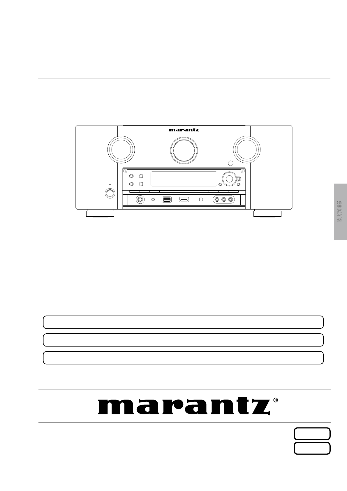
AV Surround Receiver
SR7005
For purposes of improvement, specifi cations and design are subject to change without notice.
•
Please use this service manual with referring to the operating instructions without fail.
•
Some illustrations using in this service manual are slightly different from the actual set.
•
SR7005
S00114-1V02DM/DG1009
Copyright 2010 D&M Holdings Inc. All rights reserved.
WARNING: Violators will be prosecuted to the maximum extent possible.
Ver. 2
Please refer to the
MODIFICATION NOTICE.
Page 2
MARANTZ DESIGN AND SERVICE
Using superior design and selected high grade components,
Only original
MARANTZ
parts can insure that your
MARANTZ
MARANTZ
product will continue to perform to the specifi cations for
company has created the ultimate in stereo sound.
which it is famous.
Parts for your
MARANTZ
ORDERING PARTS :
equipment are generally available to our National Marantz Subsidiary or Agent.
Parts can be ordered either by mail or by Fax.. In both cases, the correct part number has to be specifi ed.
The following information must be supplied to eliminate delays in processing your order :
1. Complete address
2. Complete part numbers and quantities required
3. Description of parts
4. Model number for which part is required
5. Way of shipment
6. Signature : any order form or Fax. must be signed, otherwise such part order will be considered as null and void.
USA
MARANTZ AMERICA, INC
100 CORPORATE DRIVE
MAHWAH, NEW JERSEY 07430
USA
JAPAN
D&M Holdings Inc.
D&M BUILDING, 2-1 NISSHIN-CHO,
KAWASAKI-KU, KAWASAKI-SHI,
KANAGAWA, 210-8569 JAPAN
EUROPE / TRADING
D&M EUROPE B. V.
P. O. BOX 8744, BUILDING SILVERPOINT
BEEMDSTRAAT 11, 5653 MA EINDHOVEN
THE NETHERLANDS
PHONE : +31 - 40 - 2507844
FAX : +31 - 40 - 2507860
CANADA
D&M Canada Inc.
5-505 APPLE CREEK BLVD.
MARKHAM, ONTARIO L3R 5B1
CANADA
PHONE : 905 - 415 - 9292
FAX : 905 - 475 - 4159
KOREA
D&M SALES AND MARKETING KOREA LTD.
2F,YEON BLDG.,
88-5, BANPO-DONG, SEOCHO-GU,
SEOUL KOREA
PHONE : +82 - 2 - 715 - 9041
FAX : +82 - 2 - 715 - 9040
CHINA
D&M SALES AND MARKETING SHANGHAI LTD.
ROOM.808 SHANGHAI AIRPORT CITY TERMINAL
NO.1600 NANJING (WEST) ROAD, SHANGHAI,
CHINA. 200040
TEL : 021 - 6248 - 5151
FAX : 021 - 6248 - 4434
NOTE ON SAFETY :
Symbol z Fire or electrical shock hazard. Only original parts should be used to replaced any part marked with symbol z .
Any other component substitution (other than original type), may increase risk of fi re or electrical shock hazard.
安全上の注意:
zがついている部品は、安全上重要な部品です。必ず指定されている部品番号の部品を使用して下さい。
SHOCK, FIRE HAZARD SERVICE TEST :
CAUTION : After servicing this appliance and prior to returning to customer, measure the resistance between either primary
AC cord connector pins (with unit NOT connected to AC mains and its Power switch ON), and the face or Front Panel of
product and controls and chassis bottom.
Any resistance measurement less than 1 Megohms should cause unit to be repaired or corrected before AC power is applied,
and verifi ed before it is return to the user/customer.
Ref. UL Standard No. 60065.
In case of diffi culties, do not hesitate to contact the Technical
Department at above mentioned address.
2
091105DM/DG
Page 3

SAFETY PRECAUTIONS
The following check should be performed for the continued protection of the customer and service technician.
LEAKAGE CURRENT CHECK
Before returning the unit to the customer, make sure you make either (1) a leakage current check or (2) a line to chassis
resistance check. if the leakage current exceeds 0.5 milliamps, or if the resistance from chassis to either side of the
power cord is less than 460 kohms, the unit is defective.
Be sure to test for leakage current with the AC plug in both polarities, in addition, in each power ON, OFF and STANDBY
mode, if applicable.
CAUTION
Please heed the points listed below during servicing and inspection.
◎Heed the cautions!
Spots requiring particular attention when servicing, such
as the cabinet, parts, chassis,etc., have cautions indicated
on labels. be sure to heed these causions and the
cautions indicated in the handling instructions.
◎Caution concerning electric shock!
(1) An AC voltage is impressed on this set, so touching
internal metal parts when the set is energized could
cause electric shock. Take care to avoid electric
shock, by for example using an isolating transformer
and gloves when servicing while the set is energized,
unplugging the power cord when replacing parts, etc.
(2) Tere are high voltage parts inside. Handle with extra
care when the set is energized.
◎ Caution concerning disassembly and
assembly!
Through great care is taken when manufacturing parts
from sheet metal, there may in some rare cases be burrs
on the edges of parts which could cause injury if fi ngers
are moved across them. Use gloves to protect your hands.
◎Only use designated parts!
The set's parts have specific safety properties (fire
resistance, voltage resistance, etc.). For replacement
parts, be sure to use parts which have the same
poroperties. In particular, for the important safety parts
that are marked z on wiring diagrams and parts lists, be
sure to use the designated parts.
◎ Be sure to mount parts and arrange the wires
as they were originally!
For safety seasons, some parts use tape, tubes or other
insulating materials, and some parts are mounted away
from the surface of printed circuit boards. Care is also
taken with the positions of the wores omsode amd clamps
are used to keep wires away from heating and high
voltage parts, so be sure to set everything back as it was
originally.
◎Inspect for safety after servicing!
Check that all screws, parts and wires removed or
disconnected for servicing have been put back in their
original positions, inspect that no parts around the area
that has been serviced have been negatively affected,
conduct an inslation check on the external metal
connectors and between the blades of the power plug,
and otherwise check that safety is ensured.
(Insulation check procedure)
Unplug the power cord from the power outlet, disconnect
the antenna, plugs, etc., and turn the power switch on.
Using a 500V insulation resistance tester, check that the
inplug and the externally exposed metal parts (antenna
terminal, headphones terminal, input terminal, etc.) is
1MΩ or greater. If it is less, the set must be inspected and
repaired.
CAUTION
Concerning important safety
parts
Many of the electric and structural parts used in the set
have special safety properties. In most cases these
properties are difficult to distinguish by sight, and using
replacement parts with higher ratings (rated power and
withstand voltage) does not necessarily guarantee that
safety performance will be poreserved. Parts with safety
properties are indicated as shown below on the wiring
diagrams and parts lists is this service manual. Be sure to
replace them with parts with the designated part number.
(1) Schematic diagrams ......Indicated by the z mark.
(2) Parts lists ......Indicated by the z mark.
Using parts other than the designated
parts could result in electric shock, fi res
or other dangerous situations.
3
Page 4
NOTE FOR SCHEMATIC DIAGRAM
WARNING:
Parts marked with this symbol z have critical characteristics. Use ONLY replacement parts recommended by the manufacture
CAUTION:
Before returning the unit to the customer, make sure you make either (1) a leakage current check or (2) a line to chassis resistance check. If the
leakage current exceeds 0.5 milliamps, or if the resistance from chassis to either side of the power cord is less than 460 kohms, the unit is defective.
WARNING:
DO NOT return the unit to the customer until the problem is located and corrected.
NOTICE:
ALL RESISTANCE VALUES IN OHM. k=1,000 OHM / M=1,000,000 OHM
ALL CAPACITANCE VALUES IN MICRO FARAD. P=MICRO-MICRO FARAD EACH VOLTAGE AND CURRENT ARE MEASURED AT NO SIGNAL
INPUT CONDITION. CIRCUIT AND PARTS ARE SUBJECT TO CHANGE WITHOUT PRIOR NOTICE.
r.
NOTE FOR PARTS LIST
Parts for which "nsp" is indicated on this table cannot be supplied.
1.
When ordering of part, clearly indicate "1" and "I" (i) to avoid mis-supplying.
2.
3.
Ordering part without stating its part number can not be supplied.
4.
Part indicated with the mark "★" is not illustrated in the exploded view.
5.
Not including General-purpose Carbon Film Resistor in the P.W.Board parts list. (Refer to the Schematic Diagram for those parts.)
6.
Not including General-purpose Carbon Chip Resistor in the P.W.Board parts list. (Refer to the Schematic Diagram for those parts.)
WARNING:
● Resistors
Ex.: RN
* Resistance
● Capacitors
Ex.: CE
* Capacity (electrolyte only)
* Capacity (except electrolyte)
・ When the dielectric strength is indicated in AC,"AC" is included after the dieelectric strength value.
Parts marked with this symbol z have critical characteristics. Use ONLY replacement parts recommended by the manufacturer.
14K
Type
Shape
and performance
RD : Carbon
RC : Composition
RS : Metal oxide film
RW: winding
RN : Metal film
RK : Metal mixture
2
Indicates number of zeros after effective number.
2-digit effective number.
1-digit effective number.
: Units: ohm
CE : Aluminum foil
electrolytic
CA : Aluminium solid
electrolytic
CS : Tantalum electrolytic
CQ: Film
CK : Ceramic
CC : Ceramic
CP : Oil
CM: Mica
CF : Metallized
CH : Metallized
・ Units:μF.
・ Units:pF
2-digit effective number, decimal point indicated by R.
04W
Type
Shape
and performance
2
Indicates number of zeros after effective number.
2-digit effective number.
2
Indicates number of zeros after efective number. (More than 2)
2-digit effective number.
2E
Power
2B : 1/8 W
2E : 1/4 W
2H : 1/2 W
3A : 1 W
3D : 2 W
3F : 3 W
3H : 5 W
1800ohm=1.8kohm1 8
1.2ohm1 R 2
1H
Dielectric
strength
0J : 6.3 V
1A : 10 V
1C : 16 V
1E : 25 V
1V : 35 V
1H : 50 V
2A : 100 V
2B : 125 V
2C : 160 V
2D : 200 V
2E : 250 V
2H : 500 V
2J : 630 V
2200μF2 2
2200pF=0.0022μF2 2
182
Resistance
F:±1%
G:±2%
J:±5%
K:±10%
M:±20%
3R2
CapacityMAllowable
G
Allowable
error
P : Pulse-resistant type
NL : Low noise type
NB : Non-burning type
FR : Fuse-resistor
F : Lead wire forming
error
F:±1%
G:±2%
J:±5%
K:±10%
M:±20%
Z:±80%
:- 20%
P : +100%
C:±0.25pF
D:±0.5pF
= : Others
FR
Others
BP
Others
HS : High stability type
BP : Non-polar type
HR : Ripple-resistant type
DL : For change and discharge
HF : For assuring high requency
U : UL part
C : CSA part
W : UL-CSA part
F : Lead wire forming
2
・ Units:μF.
1
・ Units:pF
2.2μF2 R
1-digit effective number.
2-digit effective number, decimal point indicated by R
220pF2 2
Indicates number of zeros after effective numver. (0 or 1)
2-digit effective number.
4
Page 5

TECHNICAL SPECIFICATIONS
n Audio Section
• Power amplifi er
Rated output :
Front :
125 W + 125 W (8 Ω, 20 Hz – 20 kHz with 0.08 % T.H.D.)
Center :
125 W (8 Ω, 20 Hz – 20 kHz with 0.08 % T.H.D.)
Surround :
125 W + 125 W (8 Ω, 20 Hz – 20 kHz with 0.08 % T.H.D.)
Surround back / Front height / Front wide:
125 W + 125 W (8 Ω, 20 Hz – 20 kHz with 0.08 % T.H.D.)
Maximum effective output power :
Front :
195 W + 195 W (6 Ω, 1 kHz with 10 % T.H.D.)
Center :
195 W (6 Ω, 1 kHz with 10 % T.H.D.)
Surround :
195 W + 195 W (6 Ω, 1 kHz with 10 % T.H.D.)
Surround back / Front height / Front wide:
195 W + 195 W (6 Ω, 1 kHz with 10 % T.H.D.)
Output connectors : 6 – 8 Ω
• Analog
Input sensitivity/Input impedance : 200 mV/47 kΩ
Frequency response : 10 Hz – 100 kHz — +1, –3 dB (DIRECT mode)
S/N : 96 dB (IHF–A weighted, DIRECT mode)
Distortion : 0.008 % (20 Hz ~ 20 kHz) (DIRECT mode)
Rated output : 1.2 V
• Digital
D/A output : Rated output — 2 V (at 0 dB playback)
Total harmonic distortion — 0.008 % (1 kHz, at 0 dB)
S/N ratio — 102 dB
Dynamic range — 100 dB
Digital input : Format — Digital audio interface
• Phono equalizer (PHONO input — REC OUT)
Input sensitivity : 2.5 mV
RIAA deviation : ±1 dB (20 Hz to 20 kHz)
S/N : 96 dB (IHF–A weighted, DIRECT mode)
Distortion : 74 dB (A weighting, with 5 mV input)
Rated output : 150 mV
Distortion factor : 0.03 % (1 kHz, 3 V)
n Video Section
• Standard video connectors
Input/output level and impedance : 1 Vp-p, 75 Ω
Frequency response : 5 Hz – 10 MHz — +1, –3 dB
• Color component video connector
Input/output level and impedance:
Y (brightness) signal — 1 Vp-p, 75 Ω
B / CB signal — 0.7 Vp-p, 75 Ω
P
R / CR signal — 0.7 Vp-p, 75 Ω
P
Frequency response :
5 Hz – 60 MHz — +0, –3 dB (when “Video Convert” set to “OFF”)
n HD Radio section (for U)
[FM](Note: μV at 75 Ω, 0 dBf = 1 x 10
Receiving Range :
[FM] 87.5 MHz – 107.9 MHz
Usable Sensitivity :
[FM]1.5 μV (14.8 dBf)
S/N (IHF-A) :
[FM]MONO 78 dB
STEREO 68 dB
HD 85 dB
Total harmonic Distortion (at 1 kHz) :
[FM]MONO 0.1 %
STEREO 0.1 %
HD 0.02 %
[AM]18 μV
[AM]
85 dB
[AM]
0.02 %
n Tuner section (for N, K) s
[FM](Note: μV at 75 Ω, 0 dBf = 1 x 10
Receiving Range :
[FM] 87.5 MHz – 108.0 MHz [AM]522 kHz – 1611 kHz
Usable Sensitivity :
[FM]1.2 μV (12.8 dBf) [AM]18 μV
50 dB Quieting Sensitivity :
[FM]MONO 2.0 μV (17.3 dBf)
STEREO 42 μV (34.5 dBf)
S/N (IHF-A) :
[FM]MONO 72 dB
STEREO 67 dB
Total harmonic Distortion (at 1 kHz) :
[FM]MONO 0.3 %
STEREO 0.7 %
–15
W)
[AM]530 kHz – 1710 kHz
–15
W)
n General
Power supply (for U) : AC 120 V, 60 Hz
Power supply (for N) : AC 230 V, 50 Hz
Power supply (for K) : AC 220 V, 50 Hz s
Power consumption :
700 W
0.2 W (Standby)
4.0 W (CEC standby)
Maximum external dimensions : 440 (W) x 187 (H) x 406 (D) mm
Weight : 13.0 kg
n Remote Control Unit (RC011SR)
Batteries : R03/AAA Type (two batteries)
5
Page 6
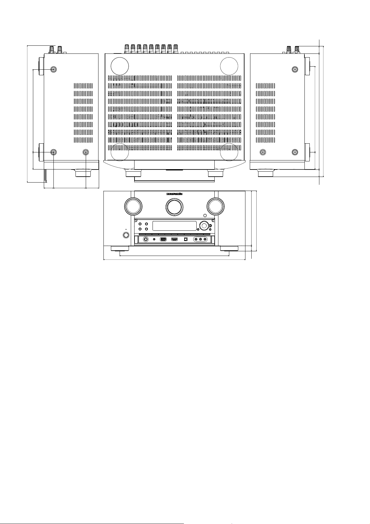
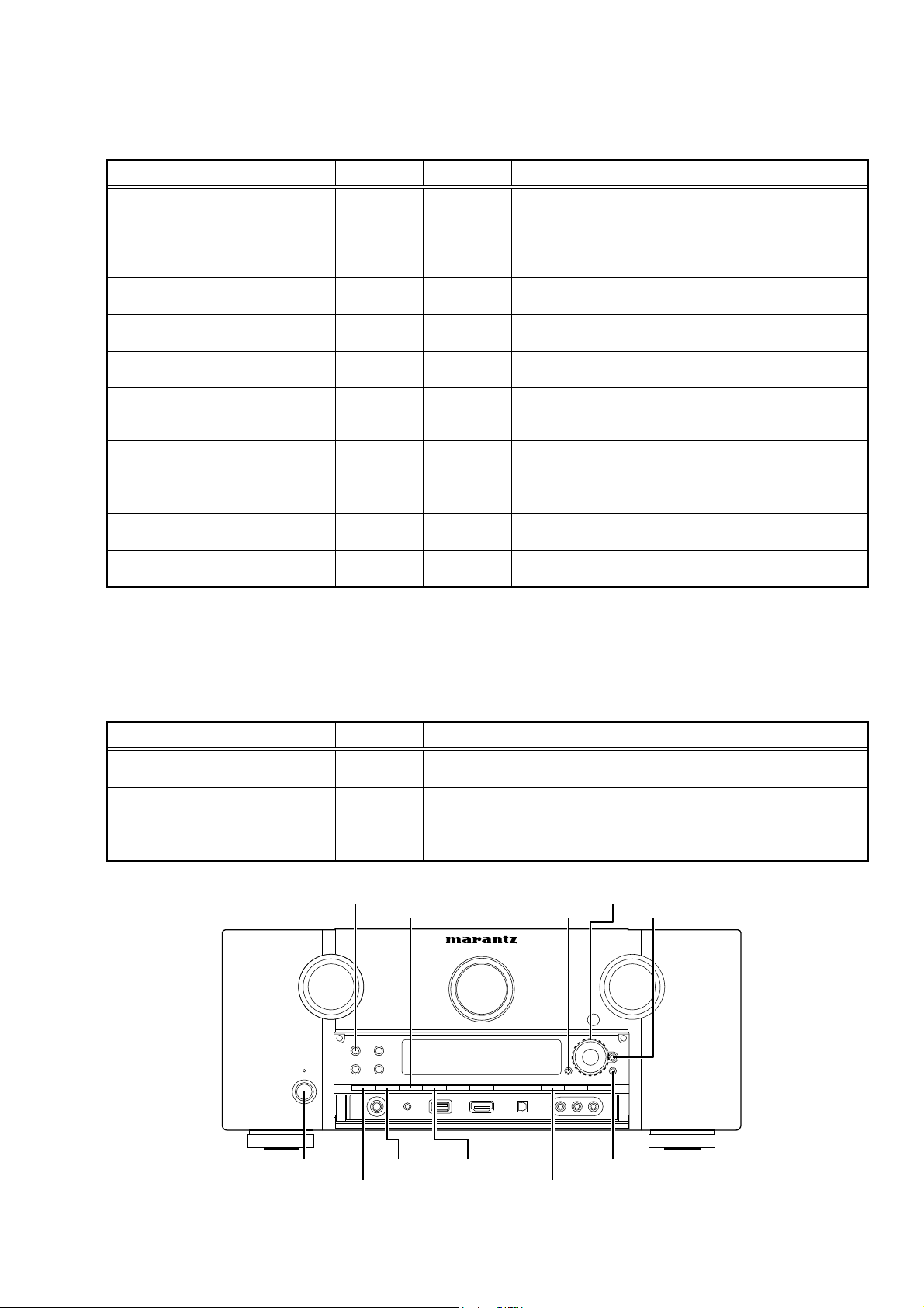
DIMENSION
s
22.5
423
52.7
257
29.8
100
40.7
340
440
187
170.5
16.5
267
360
406
52.7
23.5
6
Page 7
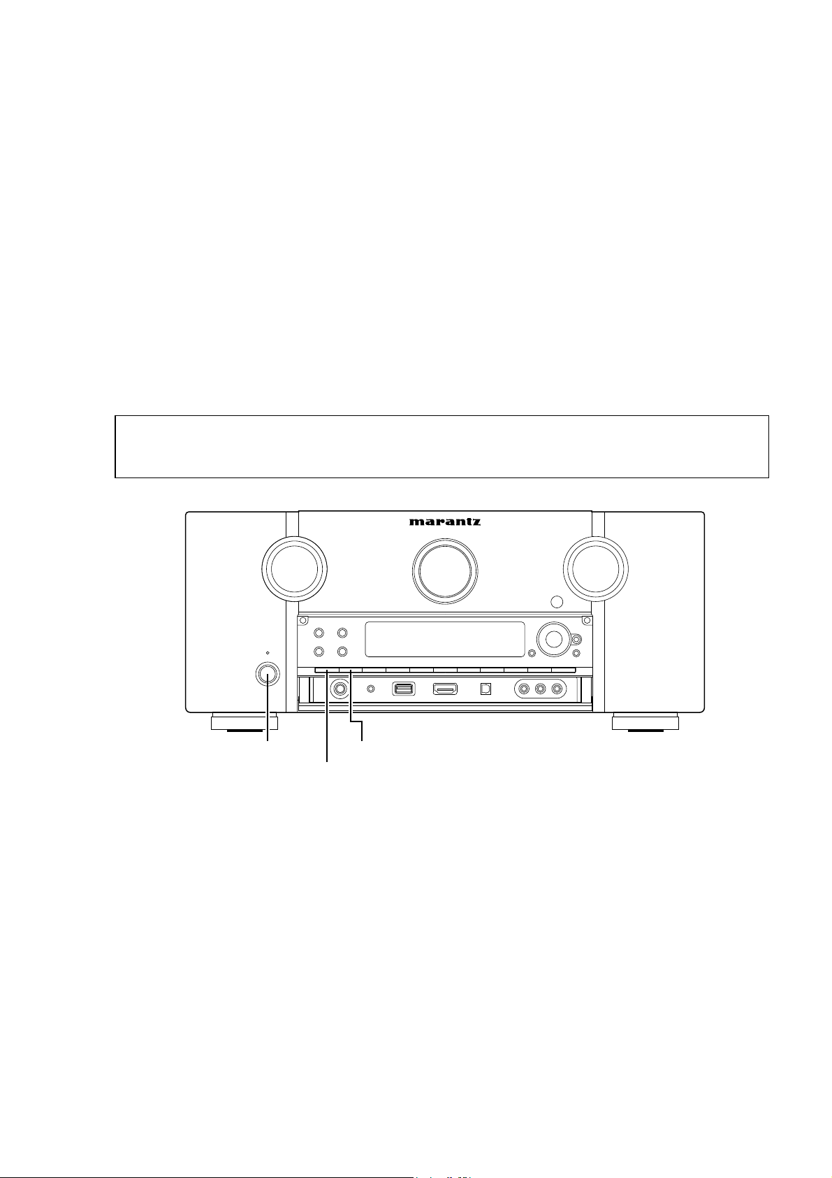
CAUTION IN SERVICING
Firmware update
• When you replace the DIGITAL UNIT ASSY (8U-310051), you need software updates.
Refer to "VERSION UPGRADE PROCEDURE OF FIRMWARE (27 - 37 page) .
Please update the following procedure.
1. First, Please update by DFW (34 - 37 page).
2. Next, Please update the latest fi rmware by DPMS (27 - 33 page).
s
Initializing AV SURROUND RECEIVER
AV SURROUND RECEIVER initialization should be performed when the μcom, peripheral parts of μcom, and Digital
P.W.B. are replaced.
1. Turn off the power using ON/STANDBY button.
2. Press ON/STANDBY button while simultaneously pressing SURROUND MODE and AUTO buttons.
3. Check that the entire display is fl ashing with an interval of about 1 second, and release your fi ngers from the 2
buttons and the microprocessor will be initialized.
Note: •If step 3 does not work, start over from step 1.
All user settings will be lost and this factory setting will be recovered when this initialization mode.
•
So make sure to memorize your setting for restoring after the initialization.
ON/STANDBY
AUTO
SURROUND MODE
Service Jigs
When you repair the printing board, you can use the following JIG (Extension cable kit).
Please order to marantz Offi cial Service Distributor in your region if necessary.
8U-110084S : EXTENSION UNIT KIT : 1 Set
(Refer to "JIG FOR SER
VICING".)
7
Page 8
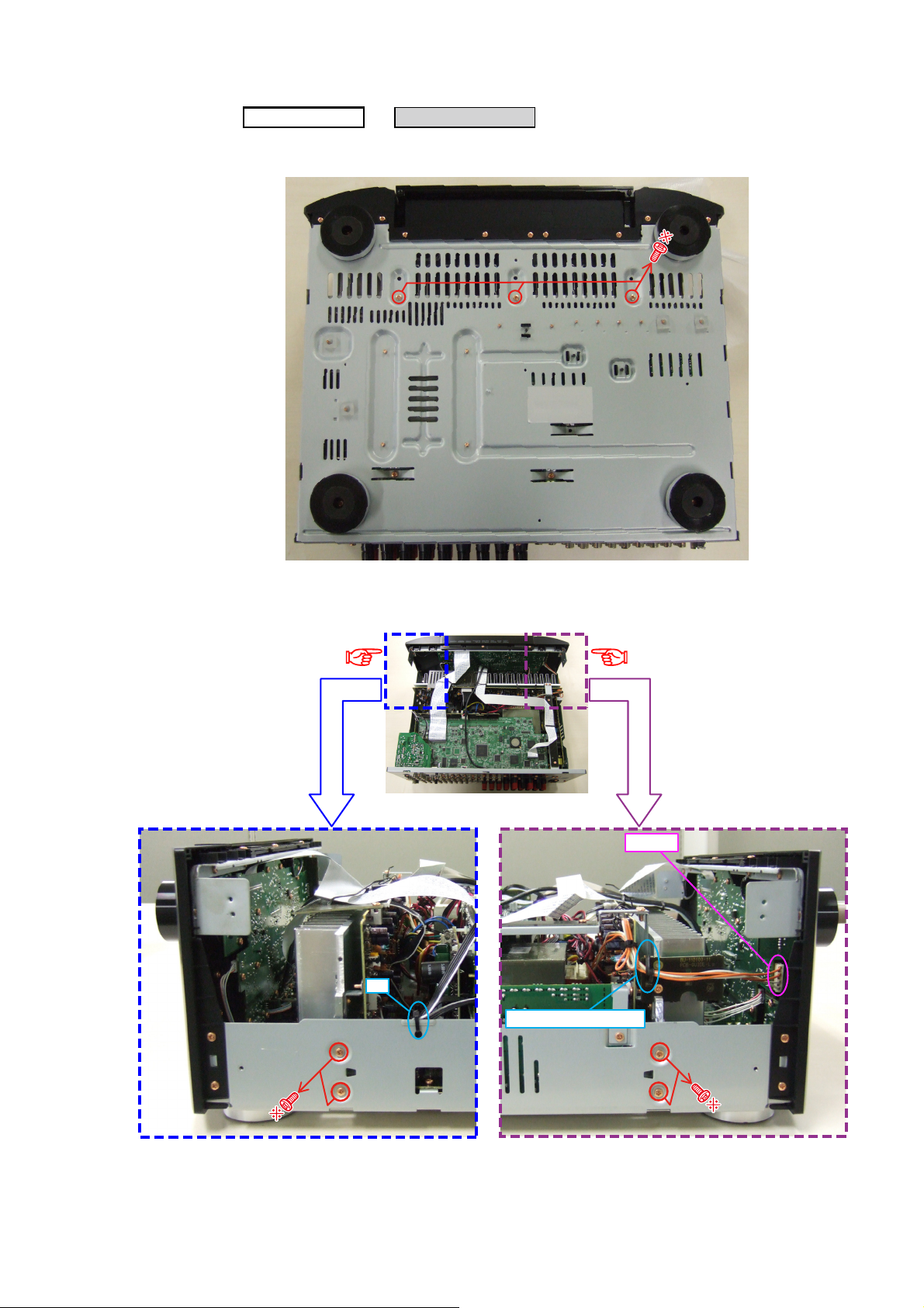
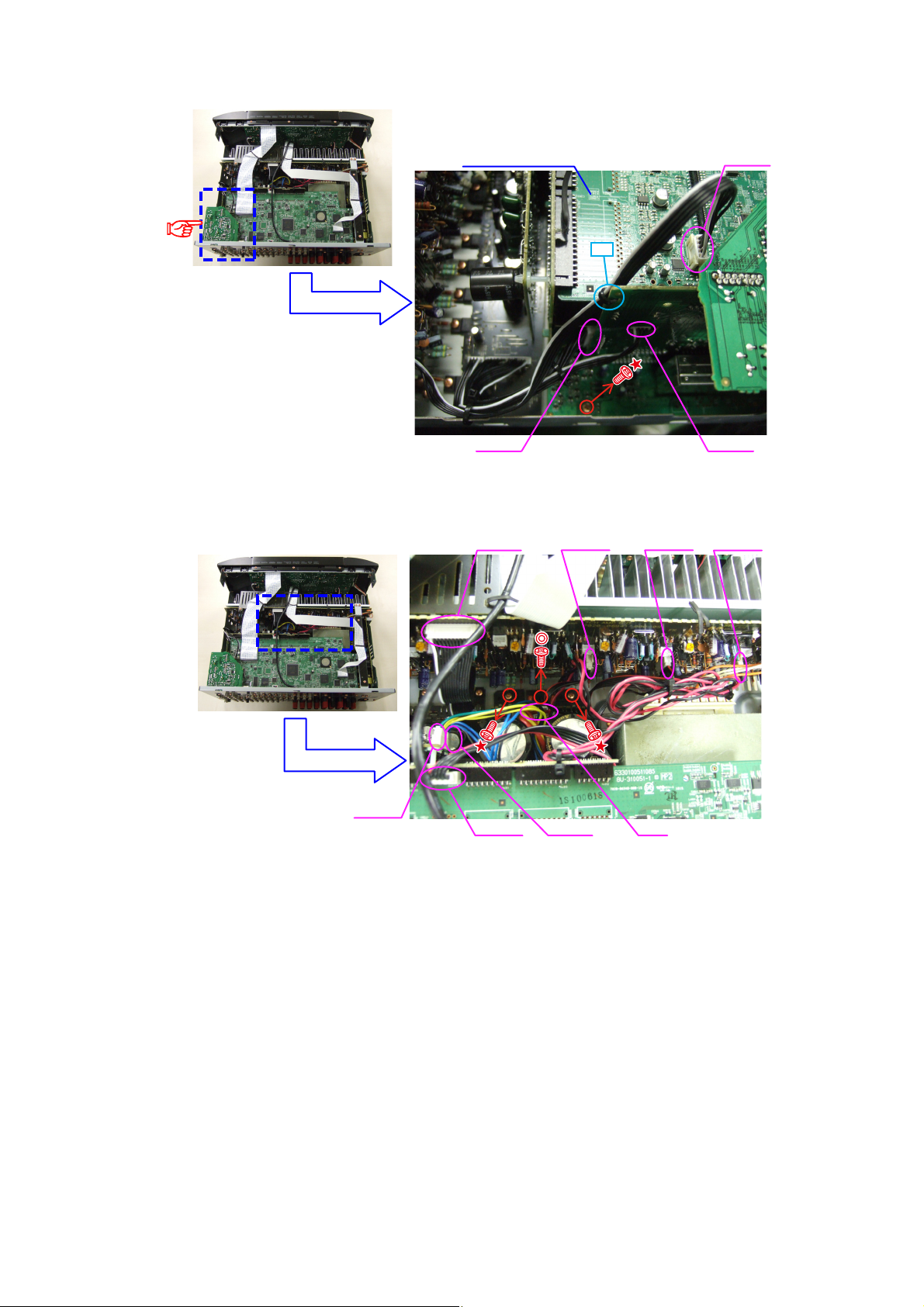
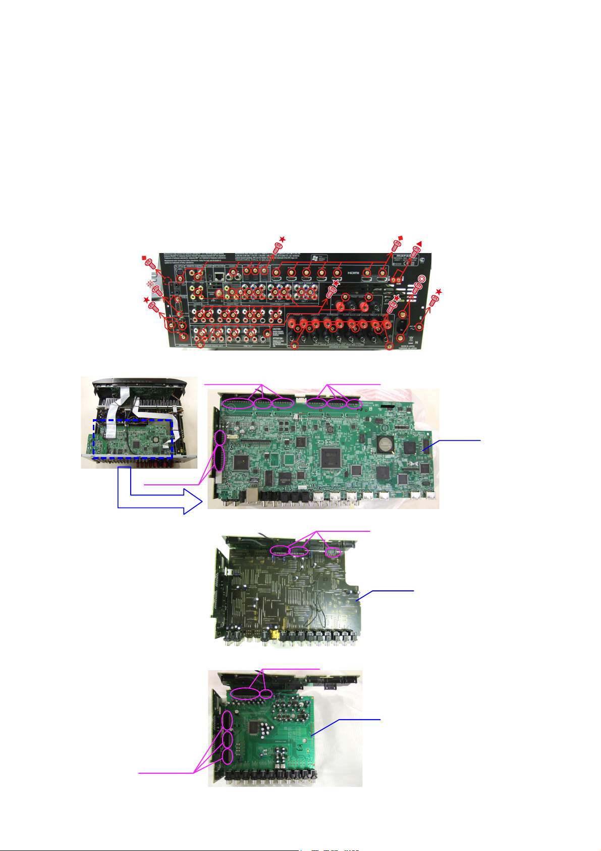
DISASSEMBLY
• Disassemble in order of the arrow of the fi gure of following fl ow.
• In the case of the re-assembling, assemble it in order of the reverse of the following fl ow.
• In the case of the re-assembling, observe "attention of assembling" it.
• If wire bundles are untied or moved to perform adjustment or parts replacement etc., be sure to rearrange them neatly
as they were originally bundled or placed afterward.
Otherwise, incorrect arrangement can be a cause of noise generation.
CABINET TOP
FRONT PANEL ASSY
Refer to "DISASSEMBLY
1. FRONT PANEL ASSY"
and "EXPLODED VIEW"
FRONT UNIT ASSY
(Ref. No. of EXPLODED VIEW : P1)
OPT UNIT
(Ref. No. of EXPLODED VIEW : P2)
H/P UNIT
(Ref. No. of EXPLODED VIEW : P3)
FRONT HDMI UNIT
(Ref. No. of EXPLODED VIEW : P4)
DOORDET UNIT
(Ref. No. of EXPLODED VIEW : P5)
HEAT SINK ASSY
Refer to "DISASSEMBLY
2. HEAT SINK ASSY"
and "EXPLODED VIEW"
7CH AMP UNIT ASSY
(Ref. No. of EXPLODED VIEW : P7)
GUIDE L UNIT
(Ref. No. of EXPLODED VIEW : P20)
GUIDE TOP UNIT
(Ref. No. of EXPLODED VIEW : P21)
PCB REG CNT/PCB REG
Refer to "DISASSEMBLY
3. PCB REG CNT/PCB REG"
and "EXPLODED VIEW"
REG UNIT
(Ref. No. of EXPLODED VIEW : P8)
REG-CNT UNIT
(Ref. No. of EXPLODED VIEW : P9)
HDMI UNIT ASSY
Refer to "DISASSEMBLY
4. HDMI UNIT ASSY"
and "EXPLODED VIEW"
FRONT CNT UNIT
(Ref. No. of EXPLODED VIEW : P10)
INPUT UNIT
(Ref. No. of EXPLODED VIEW : P11)
SPK UNIT
(Ref. No. of EXPLODED VIEW : P12)
A.AUDIO UNIT
(Ref. No. of EXPLODED VIEW : P13)
VIDEO UNIT ASSY
(Ref. No. of EXPLODED VIEW : P14)
DIGITAL UNIT
(Ref. No. of EXPLODED VIEW : P15)
SPK WIDE UNIT
(Ref. No. of EXPLODED VIEW : P16)
SIDE-CNT UNIT
(Ref. No. of EXPLODED VIEW : P17)
RS232C UNIT
(Ref. No. of EXPLODED VIEW : P18)
SIRIUS UNIT
(Ref. No. of EXPLODED VIEW : P19)
TRANS MAIN
Refer to "DISASSEMBLY
5. TRANS MAIN"
and "EXPLODED VIEW"
TRANS MAIN
(Ref. No. of EXPLODED VIEW : P22)
8
Page 9
About the photos used for descriptions in the DISASSEMBLY" section.
• The direction from which the photographs used herein were photographed is indicated at "Direction of photograph: ***"
at the left of the respective photographs.
• Refer to the table below for a description of the direction in which the photos were taken.
• Photographs for which no direction is indicated were taken from above the product.
The viewpoint of each photograph
(Photografy direction)
[View from above]
Direction of photograph: C
1. FRONT PANEL ASSY
Direction of photograph: B
Front side
Direction of photograph: D
Direction of photograph: A
Proceeding :
(1) Remove the screws.
View from bottom
CABINET TOP
FRONT PANEL ASSY
→
9
Page 10
(2) Cut the wire clamp band, then disconnect the connector wires and FFC cable, then remove the screws.
STYLEPIN : Loose
cut
STYLEPIN : Loose
FFC cable FFC cable
N4201
N1001
(3) Remove the screws.
Direction of
photograph: C
Direction of
photograph: D
Please refer to "EXPLODED VIEW" for the disassembly method of each P.W.B included in FRONT PANEL ASSY.
10
Page 11
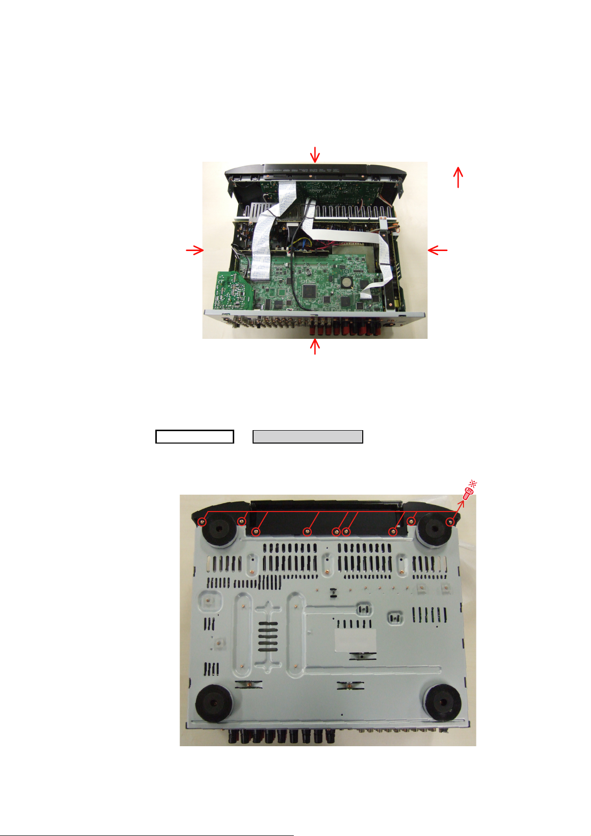
2. HEAT SINK ASSY
Proceeding :
(1) Remove the screws.
View from bottom
CABINET TOP
HEAT SINK ASSY
→
(2) Cut wire clamp band, then remove the screws. Disconnect the connector wires.
Direction of
photograph: C
cut
STYLEPIN : Loose
Direction of
photograph: D
N1001
11
Page 12
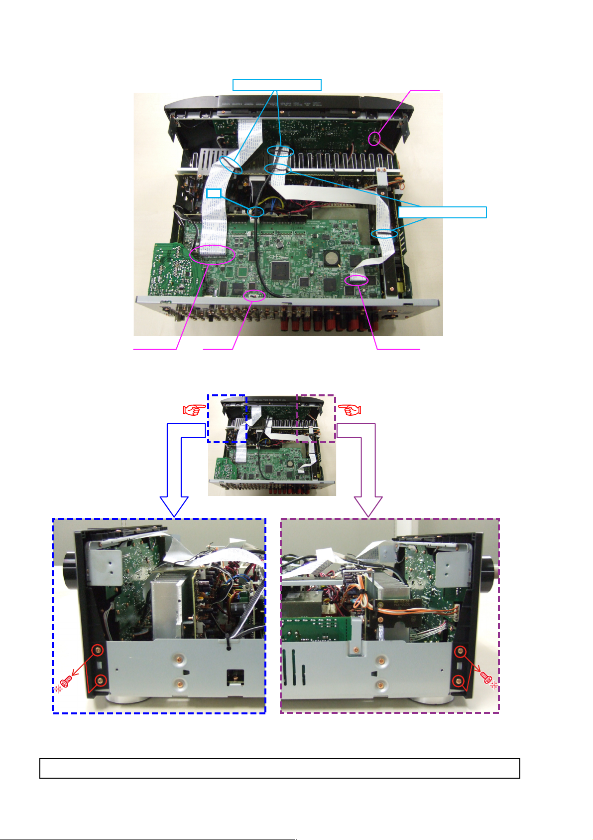
(3) Remove the screws.
Direction of photograph: A
(4) Cut the wire clamp bands, then disconnect the connector wires and FFC cable. Remove the screws, SUPPORT
PWB. and the HDMI BRACKET.
STYLEPIN : Loose
cut
N4905
FFC cable
(5) Disconnect the connector wires.
N4201
FFC cable
HEATSINK ASSY
CUSHION BRACKET
STYLEPIN : Loose
SUPPORT PWB.
HDMI BRACKET
CP401 CP402
PCB 7CH AMP
CP405CP403
Please refer to "EXPLODED VIEW" for the disassembly method of each P.W.B included in HEAT SINK ASSY.
12
Page 13
3. PCB REG CNT/PCB REG
Proceeding :
(1) Remove the screws.
CABINET TOP
HEAT SINK ASSY
→
N model
PCB REG
PCB REG CNT/PCB REG
→
s
(2) Disconnect the connector wires and connector board.
Direction of photograph: C
REG UNIT
CP104CP102
REG CNT UNIT
N2004
CP13A
Board to board
13
Page 14
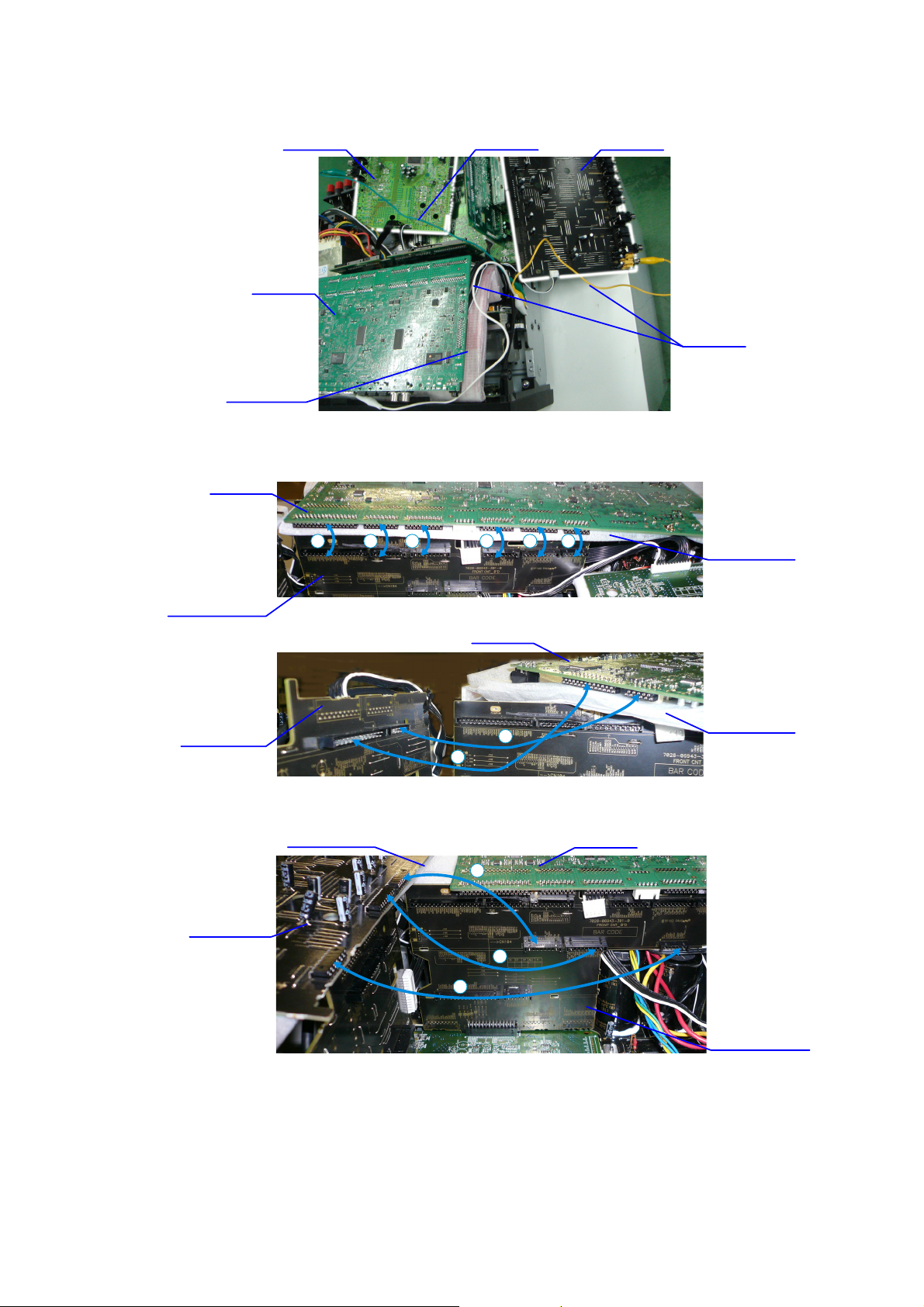
4. HDMI UNIT ASSY
Proceeding :
(1) Remove the screws, then remove the BACK PANEL and the HDMI BRACKET.
Direction of photograph: A
(2) Cut wire clamp band, then disconnect the connector wires and the FFC cables. Remove the screws and the
SUPPORT PWB.
Remove the PCB SIRIUS and the PCB RS232 from the PCB SIDE CNT(Board to board).
CABINET TOP
U model
HDMI UNIT ASSY
→
HDMI UNIT ASSY
SIRIUS UNIT
232C UNIT
FFC cable FFC cableN4201
CUSHION BRACKET
STYLEPIN : Loose
SUPPORT PWB.
BACK PANEL
HDMI BRACKET
14
Page 15
(3) Cut the wire clamp band, then disconnect the connector wires. Remove the screw.
Direction of photograph: C
(4) Remove the screws and disconnect the connector.
HDMI UNIT ASSY
CP13A
CP401
cut
CP402
CP403
N4905
N2004
CP405
CP102
CP104 CP1N4610
15
Page 16
(5) Disconnect the connector wire, then remove the screws and the P.W.B HOLDER..
P.W.B. HOLDER
CX102
(6) Remove the RAITING LABEL BASE, then remove the screws and P.W.B HOLDER.
Remove the HDMI UNIT ASSY from the main unit.
P.W.B HOLDER
View from bottom
Please refer to "EXPLODED VIEW" for the disassembly method of each P.W.B included in HDMI UNIT ASSY.
RAITING LABEL BASE
5. TRANS MAIN
Proceeding :
Please refer to "EXPLODED VIEW" for the disassembly method of each P.W.B included in TRANS MAIN.
CABINET TOP
HDMI UNIT ASSY
→
16
TRANS MAIN
→
Page 17
SPECIAL MODE
Special mode setting button
Press the ON/STANDBY button to turn on while pressing both buttons A and B at the same time.
b
Mode Button A Button B Contents
Version display
(com/DSP Error Display)
Displaying the protection history mode STATUS MENU
IInitialization mode
(Remove settings for Installer Setup.)
Initialization mode
(Includes settings for Installer Setup)
Mode for switching tuner frequency step
Mode for preventing remote control
acceptance
Panel lock mode AUTO DISPLAY
Panel lock mode
(Remove Master volume)
Cancellation of panel lock mode
Installer Setup mode MENU
STATUS RETURN
SURROUND
MODE
CURSOR UP
SURROUND
MODE
STATUS ENTER
DISPLAY
CURSOR
DOWN
AUTO
PURE
DIRECT
PURE
DIRECT
PURE
DIRECT
DISPLAY Panel lock mode is cancelled.
CURSOR
LEFT
Serial No. and fi rmware versions such as Main, Sub, DSP are
displayed in the FL manager. Errors are displayed when they
occur. (Refer to 18 page)
Displaying the protection history
(Refer to 21 page)
Backup data initialization is carried out.
(Remove settings for Installer Setup)
Backup data initialization is carried out.
(Includes settings for Installer Setup)
---N model only--Change tuner frequency step to FM:200kHz/AM:10kHzSTEP
Operations using remote control are rejected.
(Mode cancellation: Turn off power and execute the same
button operations as when performing setup.)
Operations using main unit panel buttons or master volume are
rejected.
Operations using main unit panel buttons are rejected.
Access Remote Maintenance mode via the internet.Installer
Setup is displayed on GUI/Option Menu.
NOTE:
If " S " is displayed on the fl uorescent display, the unit is set to the special developer's mode and RS-232C
communications are not possible.
Press and hold in the "STATUS" and " i " buttons for over 3 seconds with the power turned on to turn the " S " display
off. RS-232C communications are now enabled.
When power is turned on, pressing both buttons A and B at the same time for 3 seconds or more.
b
Mode Button A Button B Contents
DUAL BACKUP MEMORY (Backup) SLEEP ENTER
DUAL BACKUP MEMORY (Recovery) SLEEP MENU
DUAL BACKUP MEMORY
(Backup Clear)
SLEEP AUTO
Backup of DUAL BACKUP MEMORY is performed.
(Refer to 23 page.)
Recovery of DUAL BACKUP MEMORY is performed.
(Refer to 23 page.)
Backup of DUAL BACKUP MEMORY is cleared.
(Refer to 23 page.)
PURE DIRECT
CURSOR
DISPLAY MENU ENTER
ON/STANDBY
SURROUND MODE SLEEP
17
RETURNAUTO STATUS
Page 18
1. μcom/DSP Version display mode
1.1. Operation specifi cations
μcom/DSP version display mode:
When started up, the version information is displayed.
Starting up:
With the "RETURN" and "STATUS" buttons pressed, press the "ON/STANDBY" button to turn the power on.
Now, press the "STATUS" button to the display the 2nd item information on the FL Display.
1.2. Display Order
Error information(Refer to 1.3. Error display) qModel destination information wFirmware Package Version
Main -com/ROM version rMain 1st Boot Loader tSub -com/Sub FBL yDSP version uAudio PLD
e
iOSD FPGA Confi g oOSD Program Q0OSD font data Q1Ethernet(DM860) 1st Boot Loader, Hardware ID
Q2Ethernet(DM860) 2nd Boot Loader, Rhapsody Flag Q3Ethernet(DM860) IMAGE Q4Ethernet(DM860)MAC
ADDRESS information Q5HD RADIO SDK/HD RADIO BBP(U model only) Q6MultEQ Pro APP(Displayed when
Audyssey Pro is complete) Q7MultEQ Pro ICL(Displayed when Audyssey Pro is complete
Model destination information :
q
Upper
Lower
SR7005 *
S/N. **********
Firmware Package Version :
w
Upper
Lower
Main -com & ROM version :
e
Upper
Lower
Main 1st Boot Loader :
r
Upper
Lower
Sub -com & Sub FBL :
t
Upper
Lower
DSP ROM :
y
Upper
Lower
Firm. Package
Main :**.**
Main ROM :**.**
Main FBL :**.**
Sub :**.**
Sub FBL :**.**
DSP :**.**
Ver.:****
Audio PLD :
u
Upper
Lower
OSD FPGA Confi g :
i
Upper
Lower
Audio PLD :**.**
OSD Config:
************
18
Page 19
OSD Program :
o
Upper
Lower
OSD font data :
Q0
Upper
Lower
Ethernet(DM860) 1st Boot Loader, Hardware ID :
Q1
Upper
Lower
Ethernet(DM860) 2nd Boot Loader, Rhapsody Flag :
Q2
Upper
Lower
Ethernet(DM860) IMAGE :
Q3
Upper
Lower
OSD PRG:
************
OSD DAT:
************
*Ethernet FBL
********-AA
*Ethernet SBL
*************-BB
*Ethernet IMG
*************
Ethernet(DM860) MAC ADDRESS information :
Q4
Upper
Lower
HD RADIO SDK/HD RADIO BBP (U model only) :
Q5
Upper
Lower
MultEQ Pro APP(Displayed when Audyssey Pro is complete) :
Q6
Upper
Lower
MultEQ Pro ICL(Displayed when Audyssey Pro is complete) :
Q7
Upper
Lower
*Ethernet MAC
******-******
*HDSDK: **.**
*HDBBP:C0002.000
*MultEQ Pro APP
**.**.**.****
*MultEQ Pro ICL
**.**.**.****
19
Page 20
1.3. Error display
See the following table for each "Error information" display and its contents (status).
Display order is q,w,e,r,t.
Condition State State
Sub-com NG No response from Sub-com
q
DIR NG No response from DIR
w
When DSP boot, executing DSP reset makes no change to DSP1 FLAG0
port "H".
No change to DSP FLAG0 port "H" before issuing DSP command.
When DSP data read, executing WRITE="L" makes no change to ACK="H".
When DSP data read, executing REQ="L" makes no change to ACK="L".
DSP NG
e
EEPROM NG Error appeared in EEPROM checksum.(*** is a block address number.)
r
Both SUB/DSP
t
/EEPROM OK
When DSP data write, executing WRITE="H" makes no change to ACK="H".
When DSP data write, executing REQ="L" makes no change to ACK="L".
When DSP special code boot, executing DSP reset makes no change to
DSP FLAG0 port "H".
No change to DSP FLAG0 port "H" before issuing DSP special read
command.
No change to DSP FLAG0 port "H" before DSP version read.
SUB ERROR 01
DIR ERROR 01
DSP ERROR 01
DSP ERROR 02
DSP ERROR 03
DSP ERROR 04
DSP ERROR 05
DSP ERROR 06
DSP ERROR 11
DSP ERROR 12
DSP ERROR 13
E2PROM ERR***
(No error display, version display only)
20
Page 21
2. Errors checking mode (Displaying the protection history)
2.1. Operation specifi cations
Error mode (Displaying the protection history):
When started up, the error information is displayed.
Starting up:
●All model commonness
With the "STATUS" and "MENU" buttons pressed, press the "ON/STANDBY" button to turn the power on. The error
(protection history display) mode is set.
Now, press the "STATUS" button to turn on the FL display.
2.2. About the display on the FL display
When the "STATUS" button is pressed after setting the error (protection history display) mode, a history like the one
shown below is displayed, depending on the conditions.
(1) Normally (when there has been no protection incident)
Upper
Lower
(2) For ASO (when the last protection incident was ASO protection)
Upper
Lower
Cause: The line between speaker terminals is shorted, or use speakers having impedance less than that specifi ed.
Supplementary information: As the excess current is detected after operation of the speaker relay, the shorted
Turning on the power without correcting the abnormality will cause the protection function to work about 5 seconds
later and the power supply will be shut off.
(3) For DC (when the last protection incident was DC protection)
Upper
Lower
Cause: DC output of the power amplifi er is abnormal.
Turning on the power without correcting the abnormality will cause the protection function to work about 5 seconds
later and the power supply will be shut off.
(4) For THERMAL (when the last protection incident was THERMALprotection)
PROTECT HISTOR Y
:NO PROTECT
PROTECT HISTOR Y
:ASO
speaker terminal and the connected speaker can be identifi ed.
PROTECT HISTOR Y
:DC
Upper
Lower
Cause: The temperature of the heat sink is excessive.
Turning on the power without correcting the abnormality will cause the protection function to work about 5 seconds
later and the power supply will be shut off.
Additional causes of protection can be due to loose connections, associated components, Microprocessor, etc.
z
When the "STATUS" button is pressed again after the above protection history is displayed, the normal display reappears.
PROTECT HISTOR Y
:THERMAL
21
Page 22
2.3. Clearing the protection history
There are two ways to clear the protection history, as described below.
Start up the error (protection display) mode, display the error, then press and hold in the "ENTER" button for 3 seconds.
(1)
Upper
Lower
Upper
Lower
Upper
Lower
(2) Initialize. (Refer to "Initializing AV SURROUND RECEIVER" 7 page.)
If you want to save a backup, use the method in 2.3.(1) above.
b
PROTECT HISTOR Y
:THERMAL
Press and hold in the "ENTER" button for 3 seconds.
PROTECT HISTOR Y
CLEAR
The above is displayed and the protection history is cleared.
PROTECT HISTOR Y
:NO PROTECT
Warning indication by the POWER LED
If the power is turned off when a protection incident has been detected, the POWER LED (red) fl ashes as a warning
according to the conditions in which the protection incident occurred.
(1) ASO/DC PROTECTION : Flashes in cycles of 0.5 seconds (0.25 seconds lit, 0.25 seconds off)
(2) THERMAL PROTECTION : Flashes in cycles of 2 seconds (1 second lit, 1 second off)
22
Page 23
3. DUAL BACKUP MEMORY
This product has a Dual Backup Memory function. The conventional Backup functions to memorize, in the EEPROM
(U5302) in the circuit, a current setting of the moment the main power is turned off so that it can be restored when it
is turned ON again. Meanwhile, the DUAL BACKUP MEMORY is capable of memorizing any arbitrary setting that is
confi gured while the product is in operation so as to restore it at any time. When servicing units returned from end-users
for repairs, use this function to back up the current setting (e.g. Tuner Preset). This will enable the units to be returned to
the users after repairs, with the setting unchanged.
NOTE : If end-users use this function, the data will be overwritten.
The contents of the memory do not disappear even if you initialize this unit.
If you want to erase, please refer to 2.2. SERVICE PRECAUTIONS.
3.1. HOW TO OPERATE
-Backup-
(1) Confi gure a setting you would like to save in the MEMORY and hold down the "SLEEP" and "ENTER" buttons on the
Front Panel at the same time for 3 seconds or more.
(2) The FL Display indicates "MEMORY SAVING" while the Backup is being performed.
FLD
(3) The FL Display indicates "COMPLETE" when the Backup is completed.
FLD
-Recovery-
(1) Hold down the "SLEEP" and "MENU" buttons at the same time for 3 seconds or more.
(2) The FL Display indicates "MEMORY LOAD" while the Recovery is being performed.
FLD
(3) After the FL Display indicates "COMPLETE", the product goes into Standby mode. When the power is restored, the
Recovery is completed.
FLD
The FL Display indicates "NO BACKUP" if the DUAL BACKUP MEMORY has not been activated with no data to be
recovered saved in the Memory.
FLD
MEMORY SAVING
COMPLETE
MEMORY LOAD
COMPLETE
NO BACKUP
3.2. SERVICE PRECAUTIONS
When the Flash Rom (U5302) on the HDMI PWB is replaced make sure, in order to maintain consistency with the
Backup Memory, to clear the DUAL BACKUP MEMORY in thefollowing way :
-How to clear the Backup Memory-
(1) Hold down the "SLEEP" and "AUTO" buttons at the same time for 3 seconds or more.
(2) The FL Display indicates "BACKUP CLEAR" while the memory is being cleared.
FLD
(3) After the FL Display indicates "COMPLETE", the operation is completed.
FLD
BACKUP CLEAR
COMPLETE
23
Page 24
JIG FOR SERVICING
When you repair the printing board, you can use the following JIG (Extension cable kit).
Please order to marantz Offi cial Service. Distributor in your region if necessary.
Note: When the connection which is wrong in the JIG (EXTENSION UNIT KIT) is done it becomes cause of damage.
8U-110084S :
EXTENSION UNIT KIT
• Connection of PCB HDMI JIG
-Preparation-
8U-110084S : EXTENSION UNIT KIT : 1 Set
Insulation sheet (Do not supply it) : 3 sheet
Ground lead (Do not supply it) : 3 pcs
-Procedures-
(1) Remove the screws.
U model
(2) Disconnect the connector board.
Board to board
Board to board
Board to board
PCB HDMI
Board to board
PCB VIDEO
Board to board
PCB INPUT
Board to board
24
Page 25
(3) PCB HDMI is detached from the chassis, and it puts it into the state turned inside out.
Please pave an insulation sheet that is larger than PCB HDMI under PCB.
Connect the ground point of PCB to the chassis with a ground lead or the like.
b
PCB INPUT PCB VIDEO
Ground lead
PCB HDMI
Insulation sheet
(4) Connect the four extension jig cables.
PCB HDMI
Ground lead
PCB FRONT CNT
PCB SIDE CNT
PCB VIDEO
Insulation sheet
PCB HDMI
2
9
11
34 5678
1
Insulation sheet
Insulation sheet
PCB HDMI
10
25
PCB FRONT CNT
Page 26
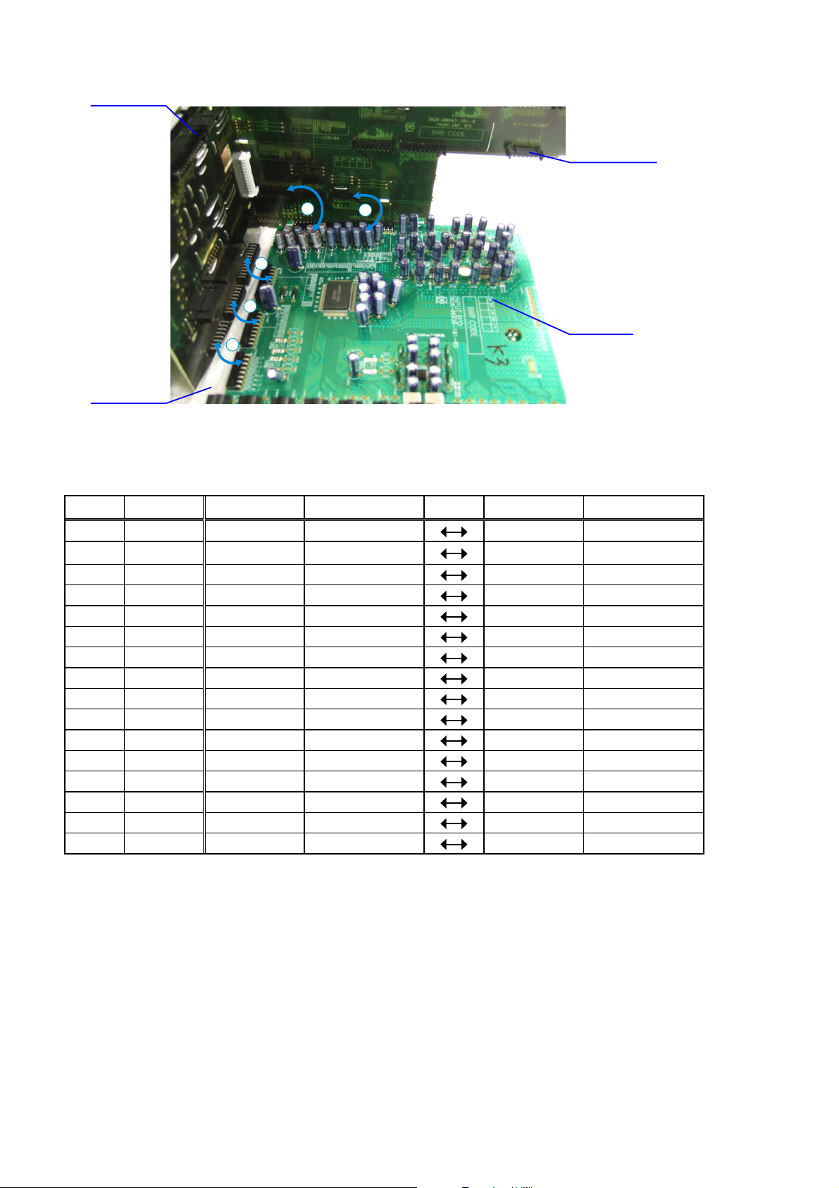
PCB SIDE CNT
PCV FRONT CNT
13
14
15
16
Insulation sheet
12
PCB INPUT
Connection table of Board to Board
No. Pin Ref. No. PCB Ref. No. PCB
q
w
e
r
t
y
u
i
o
Q0
Q11
Q2
Q3
Q4
Q5
Q6
11 pin CP3 SIDE CNT
25 pin CP4 SIDE CNT
19 pin CP105 FRONT CNT
17 pin CP106 FRONT CNT
13 pin CP107 FRONT CNT
19 pin CP108 FRONT CNT N4913 HDMI
17 pin CP109 FRONT CNT
33 pin CP110 FRONT CNT
19 pin CP111 FRONT CNT N2001 VIDEO
17 pin CP112 FRONT CNT
13 pin CP113 FRONT CNT
13 pin CP114 FRONT CNT CX3001 INPUT
33 pin CP115 FRONT CNT
19 pin CP6 SIDE CNT
17 pin CP7 SIDE CNT
15 pin CP8 SIDE CNT CX3003 INPUT
N4908 HDMI
N4907 HDMI
N4910 HDMI
N4911 HDMI
N4912 HDMI
N4914 HDMI
N4916 HDMI
N2002 VIDEO
N2003 VIDEO
CN3000 INPUT
CX3000 INPUT
CX3002 INPUT
26
Page 27
ABOUT REPLACE THE MICROPROCESSOR WITH A NEW ONE
When replaced of the U-PRO (Microprocessor) or the Flash ROM, confi rm contents of the following.
PWB Name Ref. No. Description
HDMI U5301 R5F64169DFD B SOFTWARE: Main
HDMI U5101 EN29LV160BB-70TIP B SOFTWARE: Main ROM
HDMI U5500 R5F3650KNFB B SOFTWARE: Sub
HDMI U3202 EN29LV160BB-70TIP B SOFTWARE: DSP ROM
HDMI U3000 EPM240T100C5N B SOFTWARE: Audio PLD
HDMI U1603 M25P40-VMN6PB B SOFTWARE: Video Confi g ROM
After
replaced
After replaced
A : Mask ROM (With software). No need write-in of software to the microprocessor.
B : Flash ROM (With software). Usually, no need write-in of software. But, when the software was updated, you should be
write-in of the new software to the microprocessor or fl ash ROM. Please check the software version.
C : Empty Flash ROM (Without software). You should be write-in of the software to the microprocessor or fl ash ROM.
Refer to "Update procedure" or "writing procedure", when you should be write-in the software.
s
Remark
VERSION UPGRADE PROCEDURE OF FIRMWARE
1. How to update by DPMS
You can update by downloading the latest fi rmware from the Internet.
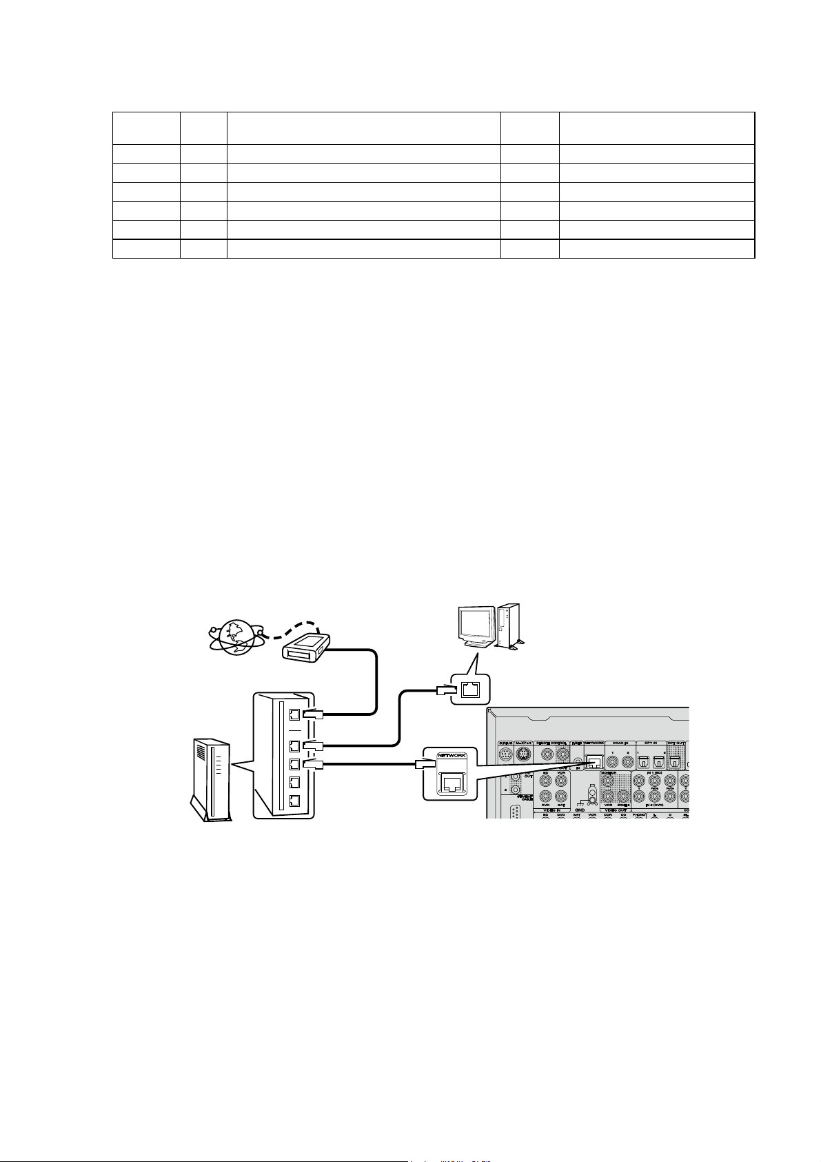
1.1. Connecting to the Network
(1) System Requirement
Internet Connection by Broadband Circuit
・
Modem
・
Router
・
Ethernet cable (CAT-5 or greater recommended)
・
(2) Setting
Internet
Computer
Router
Modem
To WAN port
To LAN port
To LAN port
ETHERNET
connector
LAN port/
Ethernet
connector
s
1.2. Check for Update and Update
Check if the latest fi rmware exists. You can also check approximately how long it will take to complete an update.
(1) Press the MENU button on the remote control to display the GUI menu.
(2) Use the cursor buttons to select "Manual Setup" → "Option Setup" → "Firmware Update" → "Update Check".
(3) Press the ENTER buttom.
The latest version of the fi rmware uploaded to the web is displayed.
・
If the latest fi rmware version is on the web, proceed to (4).
・
If the latest fi rmware is already installed, press the MENU button to close the menu.
・
(4) Use the cursor buttons to select "Update", then press the ENTER button.
During update, the power indicator lights red and the GUI screen is shut down. And a rough remaining time is
・
indicated on the display.
When updating is complete the power indicator turns off and normal status is resumed.
・
(5) Press the MENU button to close the menu.
27
Page 28
--- Cautions on Firmware Update ---
In order to use these functions, you must have the correct system requirements and settings for a broadband Internet
・
connection.
Do not turn off the power until updating is completed.
・
Even with a broadband connection to the Internet, approximately about 1 hour is required for the updating procedure
to be completed.
Once updating starts, normal operations on the SR7005 cannot be performed until updating is completed. Also, setting
items of the GUI menu of SR7005 or setting items of the image adjustment may be initialized.
Make a note of the settings before updating, and set them again after updating.
1.3. About the error code
See the chart below for error codes, details of faults, and coping strategies when fi rmware updates are performed
through DPMS (D&M Product Management Server).
Error
Code
01
02
03
04
05
06
07
Details of Error code Display Coping strategies
Log-in to DPMS has failed.
Line, etc., is busy when logging into
DPMS.
Connection to DPMS failed.
Firmware fi le data was requested
but error message was received.
Firmware fi le data was requested
but it timed out.
Firmware fi le data was requested
but error message was received.
All fi rmware fi le data was requested
but it timed out.
Login failed
01
Server is busy
02
Connection fail
03
Connection fail
04
Connection fail
05
Connection fail
06
Connection fail
07
Reset and update again.
Carry out the update in an environment that
has little network load.
Carry out the update in an environment
that has little network load.
Check the network connection.
Carry out the update in an environment
that has little network load.
Check the network connection.
Carry out the update in an environment
that has little network load.
Check the network connection.
Carry out the update in an environment
that has little network load.
Check the network connection.
Carry out the update in an environment
that has little network load.
Check the network connection.
Carry out the update in an environment
that has little network load.
Main CPU fi rmware fi le data was
requested but error message was
08
received.
Main CPU fi rmware fi le data was
09
requested but it timed out.
Error (NG) message received when
0A
downloading Main CPU fi rmware.
Error (line congestion) message
received when downloading Main
0B
CPU fi rmware.
Error (connection failure) message
received when downloading Main
0C
CPU fi rmware.
Connection fail
08
Connection fail
09
Download fail
0A
Download fail
0B
Download fail
0C
28
Check the network connection.
Carry out the update in an environment
that has little network load.
Check the network connection.
Carry out the update in an environment
that has little network load.
Check the network connection.
Carry out the update in an environment
that has little network load.
Check the network connection.
Carry out the update in an environment
that has little network load.
Check the network connection.
Carry out the update in an environment
that has little network load.
Page 29
Error
Code
0D
10
Details of Error code Display Coping strategies
Data acquisition failed (timed out)
when downloading Main CPU
fi rmware. Received Package
Version is wrong.
Main CPU failed to receive fi rmware
for rewriting sent from
DM860 (when timed out).
Connection fail
0D
Main ***min
Updating fail 10
Check the network connection.
Carry out the update in an environment
that has little network load.
Turn the power off then back on.
Updating starts automatically.
Main CPU failed to receive fi rmware
for rewriting sent from DM860 (when
11
an error )
There was invalid data in the
fi rmware for rewriting sent from
12
DM860 to Main CPU (when a
Check Sum error).
The deletion of block data failed
13
before rewriting Main CPU.
The rewriting of block data failed
14
when rewriting Main CPU.
The data verifi cation was invalid
15
after rewriting Main CPU.
Log-in to DPMS has failed when
rewriting fi rmware such as Sub
36
CPU, DSP, FPGA, and PLD.
Line, etc., is busy when logging
into DPMS when rewriting fi rmware
37
such as Sub CPU, DSP, FPGA, and
PLD.
Main ***min
Updating fail 11
Main ***min
Updating fail 12
Main ***min
Erase fail 13
Main ***min
Updating fail 14
Main ***min
UpdateCheckNG 15
Login failed
36
Server is busy
37
Turn the power off then back on.
Updating starts automatically.
Turn the power off then back on.
Updating starts automatically.
Turn the power off then back on.
Updating starts automatically.
Turn the power off then back on.
Updating starts automatically.
Turn the power off then back on.
Updating starts automatically.
Carry out the update in an environment
that has little network load.
Carry out the update in an environment
that has little network load.
Connection to DPMS failed when
rewriting fi rmware such as Sub
38
CPU, DSP, FPGA, and PLD.
Connection to DPMS timed out
when rewriting fi rmware such as
39
Sub CPU, DSP, FPGA, and PLD.
Error (NG) message received
when downloading fi rmware when
3A
rewriting Main CPU.
Error (line congestion) message
received when downloading
3B
fi rmware when rewriting Main CPU.
Error (connection failure) message
received when downloading
3C
fi rmware when rewriting Main CPU.
Log-in to DPMS has failed when
rewriting fi rmware such as Sub
50
CPU, DSP, FPGA, and PLD.
Line, etc., is busy when logging
into DPMS when rewriting fi rmware
51
such as Sub CPU, DSP, FPGA, and
PLD.
Connection fail
38
Connection fail
39
Download fail
3A
Download fail
3B
Download fail
3C
Sub ***min
Login failed 50
Sub ***min
Server is busy51
Check the network connection.
Carry out the update in an environment
that has little network load.
Check the network connection.
Carry out the update in an environment
that has little network load.
Turn the power off then back on.
Updating starts automatically.
Carry out the update in an environment
that has little network load.
Turn the power off then back on.
Updating starts automatically.
Carry out the update in an environment
that has little network load.
Turn the power off then back on.
Updating starts automatically.
Carry out the update in an environment
that has little network load.
Carry out the update in an environment
that has little network load.
Carry out the update in an environment
that has little network load.
29
Page 30
Error
Code
Details of Error code Display Coping strategies
Connection to DPMS failed when
rewriting fi rmware such as Sub
52
CPU, DSP, FPGA, and PLD.
Error message received regarding
fi rmware data after logging in to
54
DPMS when rewriting fi rmware such
as Sub CPU, DSP, FPGA, and PLD.
When rewriting fi rmware such as Sub
CPU, DS
55
was made for fi rmware data after
logging in to DPMS, but it timed out.
Failure to download fi rmware after
logging in to DPMS when rewriting
56
fi rmware such as Sub CPU, DSP,
FPGA, and PLD.
Firmware download error received
(line congestion) after logging in to
57
DPMS when rewriting fi rmware such
as Sub CPU, DSP, FPGA, and PLD.
Firmware download error received
(connection failure) after logging in to
58
DPMS when rewriting fi rmware such
as Sub CPU, DSP, FPGA, and PLD.
NACK received when "C" command
sent to Sub CPU, DSP, FPGA, PLD
5A
etc.
P, FPGA,
and PLD, request
Sub ***min
ConnectionFail52
Sub ***min
Updating fail 54
Sub ***min
Updating fail 55
Sub ***min
Download fail 56
Sub ***min
Server is busy57
Sub ***min
ConnectionFail58
Sub ***min
ConnectionFail5A
Check the network connection.
Carry out the update in an environment
that has little network load.
Turn the power off then back on.
Updating starts automatically.
Carry out the update in an environment
that has little network load.
Turn the power off then back on.
Updating starts automatically.
Carry out the update in an environment
that has little network load.
Turn the power off then back on.
Updating starts automatically.
Carry out the update in an environment
that has little network load.
Turn the power off then back on.
Updating starts automatically.
Carry out the update in an environment
that has little network load.
Turn the power off then back on.
Updating starts automatically.
Carry out the update in an environment
that has little network load.
Turn the power off then back on.
Updating starts automatically.
NACK received when "L" command
sent to Sub CPU, DSP, FPGA, PLD
5B
etc.
Sub CPU, DSP, FPGA, PLD etc.
failed to receive fi rmware for
5C
rewriting sent from DM860 (when
timed out).
Sub CPU, DSP, FPGA, PLD etc.
failed to receive fi rmware for
5D
rewriting sent from DM860 (when
an error).
Invalid data in fi rmware such as
Sub CPU, DSP, FPGA, and PLD for
5E
rewriting sent from DM860 (when a
Check Sum error).
Invalid data in fi rmware such as
Sub CPU, DSP, FPGA, and PLD for
5F
rewriting sent from DM860 (invalid
data received).
NACK received when "P" command
sent to Sub CPU, DSP, FPGA, PLD
60
etc.
NACK received when "I" command
sent to Sub CPU, DSP, FPGA, PLD
61
etc.
Sub ***min
Updating fail 5B
Sub ***min
Updating fail 5C
Sub ***min
Updating fail 5D
Sub ***min
Updating fail 5E
Sub ***min
Updating fail 5F
Sub ***min
Updating fail 60
Sub ***min
UpdateCheckNG 61
Turn the power off then back on.
Updating starts automatically.
Turn the power off then back on.
Updating starts automatically.
Turn the power off then back on.
Updating starts automatically.
Turn the power off then back on.
Updating starts automatically.
Turn the power off then back on.
Updating starts automatically.
Turn the power off then back on.
Updating starts automatically.
Turn the power off then back on.
Updating starts automatically.
Start failure of Sub μ-com.
62
Failure to acquire serial fl ash data
80
and before deleting serial fl ash.
Sub ***min
Updating fail 62
OSD ***min
Updating fail 80
30
Turn the power off then back on. Updating
starts automatically.
Turn the power off then back on.
Updating starts automatically.
Page 31

Error
Code
Details of Error code Display Coping strategies
Failure to delete data before
81
rewriting serial fl ash.
Failure to receive fi rmware for serial
fl ash rewriting sent by DM860 (when
82
timed out).
Failure to receive fi rmware for serial
fl ash rewriting sent by DM860 (when
83
an error).
Failure to receive fi rmware for serial
fl ash rewriting sent by DM860 (when
84
a Check Sum error).
Failure to receive fi rmware for serial
fl ash rewriting sent by DM860 (when
85
invalid data received).
Failure to rewrite when writing data
86
in serial fl ash.
Failure to acquire (Application
Mode) IP address before rewriting
A0
DM860 (AutoIP).
OSD ***min
Updating fail 81
OSD ***min
Updating fail 82
OSD ***min
Updating fail 83
OSD ***min
Updating fail 84
OSD ***min
Updating fail 85
OSD ***min
Updating fail 86
Ether IMG ***min
ConnectionFailA0
Turn the power off then back on.
Updating starts automatically.
Turn the power off then back on.
Updating starts automatically.
Turn the power off then back on.
Updating starts automatically.
Turn the power off then back on.
Updating starts automatically.
Turn the power off then back on.
Updating starts automatically.
Turn the power off then back on.
Updating starts automatically.
Check the network connection.
Carry out the update in an environment
that has little network load.
Failure to acquire (Application
Mode) IP address before rewriting
A1
DM860 (when timed out).
Notifi cation of invalid login via DPMS
access when rewriting DM860
A2
related fi rmware (Application Mode).
Notifi cation of line congestion
via DPMS access when rewriting
A3
DM860 related fi rmware (Application
Mode).
Notifi cation of connection failure
via DPMS access when rewriting
A4
DM860 related fi rmware (Application
Mode).
Firmware data error message
received after DPMS login when
A6
rewriting DM860 related fi rmware
(Application Mode).
When rewriting DM860 related
fi rmware (Application Mode),
A7
request was made for fi rmware data
after DPMS login but it timed out.
Failure to acquire (Boot Loader
Mode) IP address before rewriting
A8
DM860 (AutoIP).
Ether IMG ***min
ConnectionFailA1
Ether IMG ***min
Login failed A2
Ether IMG ***min
Server is busyA3
Ether IMG ***min
ConnectionFailA4
Ether IMG ***min
Updating fail A6
Ether IMG ***min
Updating fail A7
Ether IMG ***min
ConnectionFailA8
Check the network connection.
Carry out the update in an environment
that has little network load.
Check the network connection.
Carry out the update in an environment
that has little network load.
Check the network connection.
Carry out the update in an environment
that has little network load.
Check the network connection.
Carry out the update in an environment
that has little network load.
Turn the power off then back on.
Updating starts automatically.
Carry out the update in an environment
that has little network load.
Turn the power off then back on.
Updating starts automatically.
Carry out the update in an environment
that has little network load.
Check the network connection.
Carry out the update in an environment
that has little network load.
Failure to acquire (Boot Loader
Mode) IP address before rewriting
A9
DM860 (when timed out).
Notifi cation of invalid login via
DPMS access when rewriting
AA
DM860 related fi rmware (Boot
Loader Mode).
Ether IMG ***min
ConnectionFailA9
Ether IMG ***min
Login failed AA
31
Check the network connection.
Carry out the update in an environment
that has little network load.
Check the network connection.
Carry out the update in an environment
that has little network load.
Page 32

Error
Code
AB
AC
AE
AF
B0
B2
Details of Error code Display Coping strategies
Notifi cation of line congestion
via DPMS access when rewriting
DM860 related fi rmware (Boot
Loader Mode).
Notifi cation of connection failure
via DPMS access when rewriting
DM860 related fi rmware (Boot
Loader Mode).
Firmware download error message
received (when download fails)
when rewriting DM860 related
fi rmware (Boot Loader Mode).
Firmware download error message
received (line congestion) when
rewriting DM860 related fi rmware
(Boot Loader Mode).
Firmware download error message
received (connection failure) when
rewriting DM860 related fi rmware
(Boot Loader Mode).
Error message received when
rewriting DM860 related fi rmware.
Ether IMG ***min
Server is busyAB
Ether IMG ***min
ConnectionFailAC
Ether IMG ***min
Download fail AE
Ether IMG ***min
Server is busyAF
Ether IMG ***min
ConnectionFailB0
Ether IMG ***min
Updating fail B2
Check the network connection.
Carry out the update in an environment
that has little network load.
Check the network connection.
Carry out the update in an environment
that has little network load.
Turn the power off then back on.
Updating starts automatically.
Carry out the update in an environment
that has little network load.
Turn the power off then back on.
Updating starts automatically.
Carry out the update in an environment
that has little network load.
Turn the power off then back on.
Updating starts automatically.
Carry out the update in an environment
that has little network load.
Turn the power off then back on.
Updating starts automatically.
Carry out the update in an environment
that has little network load.
32
Page 33

Device display when fi rmware updated
Target of devide when fi rmware updated.
Target of device
Main
Sub
Audio PLD
DSP
OSD
(FPGA/Program/Font Data)
DM860 Boot Loader
DM860 Image
Display
Main ***min
Updating
Sub ***min
Updating
APLD ***min
Updating
DSP ***min
Updating
OSD ***min
Updating
Ether SBL ***min
Updating
Ether IMG ***min
Updating
Error cpde
10~15
36~3C
50~52
54~58
5A~62
50~52
54~58
5A~62
50~52
54~58
5A~62
50~52
54~58
5A
62
80~86
A0~A4
A6~AC
AE~B0
B2
A0~A4
A6~AC
AE~B0
B2
33
Page 34

2. How to update by DWF
2.1. Preparations before starting the operation2
(1) Personal Computer (Installed "DFW_0005_SR7005_(Rev.1.0.13)_exe").
(2) RS-232 cable (9P (Male), Straight).
2.2. Connection of the AV receiver
(1) Confi rm the power on/off switch of the AV receiver is turning off.
(2) Connect the RS-232C cable from PC with the AV receiver.
RS-232C Cable
PC
2.3. Turn on the AV receiver
Operate the following. Turn on the AV receiver.
(1) Connect the power cable to the AC outlet while simultaneously pushing the "CURSOR
button of the front panel.
(2) Confi rm the power indicator is green and “WRITTING” is displayed in the front panel.
2.4. Run the D&M Firmware Writer
Run the "DFW_0005_SR7005_(Rev.1.0.13)" on desktop of PC.
"
button and the "RETURN"
0
34
Page 35

2.5. Communication check
(1) Click the “Check Comm.” button.
(2) When connection is good, then you can see the “Communication check OK.” message.
(3) If connection is not good, then you can see the “Communication error!” message.
Please confi rm the following
(a) Check the connection of the AV receiver and PC. (refer to “2.2. Connection of the AV receiver” )
(b) Check the operation mode of the AV receiver. (refer to “2.3. Turn on the AV receiver”)
(c) Check the selection of the RS-232C port number of PC.
35
Page 36

2.6. Download the fi rmware
(1) Click the "Load" button.
(2) Download the fi rmware from the specifi ed download source to PC.
2.7. Complete the fi rmware updating
(1) Click the “Update” button.
(2) When writing of the fi rmware is completed, the power of this unit turns on automatically and you can see the “Update
completed” message.
(3) If you can’t complete the fi rmware update, please retry the fi rmware update from “2.3. Turn on the AV receiver”.
36
Page 37

2.8. Notice:
Please keep the following notice for fi rmware update.
(a) Keep the PC environment
(b) Avoid the communication cable from the electrical noise source.
(e.g. telephone cable, AC line, a fl uorescent light)
(c) Don’t remove cable during update.
(d) Don’t turn off the power during update.
(e) Don’t run other PC application during update.
(f) Stop the resident program on PC (Virus checker and System check utilitu, etc)
(g) Stop the screen saver on PC.
(h) Stop the power save ability on PC.
(i) In case of laptop PC, Use the AC adaptor.
Confi rming the fi rmware’s number after upgraded
After completion of the updating operation, the new version number can confi rmed by starting up theSR7005 according
to the following procedure.
With the following operation, the SR7005 can be set to the Flash ROM Version-Number Confi emation mode.
Turn on power switch while simultaneously pressing "STATUS" and "RETURN" buttons on the front panel. Every time the
"STATUS" button is pressed, version number of the Model, Main, Sub, … are indicated on the front panel section in the
following order.
37
Page 38
SURROUND MODES AND PARAMETERS
LFE
z8
z7
D. Comp
SS
DRC
HT-EQ
Subwoofer
SS
z6
z5
z4
z4
D SSS
D SSS
DSSSS
DSSS
DSSS
z1
D
L/R
Front wide
z1
D
L/R
Front height
z1
L/R
Surround back
Channel output Surround Parameter
L/R
Surround
Center
S D
SDDD
L/R
Front
z1
D
z1
D
z1
SDDD DS S
S D
SDDD
S DSSSS
z3
z3
z3
D
D
D
z2
z2
z2
SDDDD DS SS
SDDDD DS SS
SDDDD DSS S
SDDDD DS SS
SDDDD DS SS
SDDDD DS SS
SDDD DSSS
SDD D
SDD D
SDDDD DS SS
S
SDDD DS SS
SDDD DS
S DS
Surround mode
DOLBY DIGITAL Plus
DOLBY TrueHD
DTS SURROUND
DTS 96/24
DTS-HD
DTS Express
MULTI CH STEREO
NEURAL
DOLBY VIRTUAL SPEAKER
PURE DIRECT (2channel)
PURE DIRECT (Multi-channel)
DIRECT (2channel)
DIRECT (Multi-channel)
STEREO
MULTI CH IN
DOLBY PRO LOGIC gz SDD D DSSS
DOLBY PRO LOGIC gx SDDD DSSS
DOLBY PRO LOGIC g SDD DSSS
Symbols in the table
S This indicates the audio output channels or surround parameters that can be set.
D This indicates the audio output channels. The output channels depend on the settings of “Speaker Config.”-.
DOLBY PRO LOGIC g A-DSX SDD D
DTS NEO:6
DTS NEO:6 A-DSX
Audyssey DSX
DOLBY DIGITAL
DOLBY HEADPHONE
z1 A signal for each channel contained in an input signal is output as audio.
z2 If “Audyssey DSX” is set to “ON–Height–”, sound is output from the front height speakers.
z3 If “Audyssey DSX” is set to “ON–Wide–”, sound is output from the front wide speakers.
z4 Only when “Subwoofer Mode” is set to “LFE+Main”, sound is output from the subwoofer.
z5 For HD Audio whose sampling frequency of an input signal is more than 96 kHz, this sound parameter cannot be set.
z6 This item can be selected when a Dolby TrueHD signal is played.
38
z7 This item can be selected when a Dolby Digital or DTS signal is played.
z8 This item can be selected when a Dolby Digital or DTS signal or DVD-Audio is played.
Page 39

z13
M-DAX
z10
Soundstage
Audyssey DSX™
®
z12
Dynamic Volume
z10
®
z11
Dynamic EQ
Audyssey Settings
XT
®
z9
Tone
only
NEO:6 Music mode
Surround Parameter
PRO LOGIC g/gx Music mode only
Panorama Dimension C.Width C.Image MultEQ
SSSSS
SSSS S
SSSSS
SSSSS
SSSSS
SSSSS
SSSSS
SSSSS
SSSSS
SSSSS
SSSSSSS
SSSSSSS
SSSS S
SSSS S
SSSS S
SSSS S
Height Gain
Surround mode
PURE DIRECT (2 channel)
PURE DIRECT (Multi-channel)
DIRECT (2 channel)
DIRECT (Multi-channel)
STEREO
MULTI CH IN
DOLBY PRO LOGIC gz S SSSS S
DTS NEO:6 A-DSX
Audyssey DSX
DOLBY DIGITAL
DOLBY DIGITAL Plus
DOLBY TrueHD
DTS SURROUND
DTS 96/24
DTS-HD
DTS Express
MULTI CH STEREO
NEURAL
DOLBY VIRTUAL SPEAKER
DOLBY PRO LOGIC gx SSS SSSSSS
DOLBY PRO LOGIC g SSS SSSSSS
DOLBY PRO LOGIC g A-DSX SSS SSSSSS
DTS NEO:6
DOLBY HEADPHONE
z9 This item cannot be set when “Dynamic EQ” is set to “ON”.
z10 For HD Audio whose sampling frequency of an input signal is more than 96 kHz, this sound parameter cannot be set.
z11 This item cannot be set when “MultEQ XT” is set to “OFF” or “Manual”.
z12 This item cannot be set when “Dynamic EQ” is set to “OFF”.
z13 This item can be set when the input signal is analog, PCM 48 kHz or 44.1 kHz.
39
Page 40

DOLBY
DIGITAL
DOLBY
DIGITAL
DOLBY
DIGITAL
DOLBY
DIGITAL EX
DOLBY
DIGITAL EX
DOLBY
DOLBY
DTS 96/24
DTS
(2ch)
(4/3ch)
(5.1/5/4ch)
Flag)
(With no
(With Flag)
DIGITAL Plus
TrueHD
(5.1ch)
Input signal types and formats
MTRX
DTS ES
(With Flag)
DSCRT
DTS ES
(With Flag)
DTS
EXPRESS
High
DTS-HD
Resolution
Audio
Master
DTS-HD
(2ch)
LINEAR PCM
PCM DTS-HD DTS DOLBY DOLBY DIGITAL
(multi ch)
LINEAR PCM
ANALOG
Audio
z5 S
z5 S
z5 SSS
z5 S
z1z3 S
z1z3 S
SSSSSSS
SS S
SS S
z5 S
z5 SS S
z5 SS S
z1z3 SSS SSS
z5 S
z5 S
z5 SSSS
z1z3 SSSS
z1z3 SS
z4 SS S
Surround mode NOTE
DTS-HD MSTR
DTS-HD HI RES
DTS ES DSCRT6.1
DTS ES MTRX6.1
DTS SURROUND
Symbols in the table
S This indicates the selectable surround mode.
DTS SURROUND
DTS 96/24
DTS EXPRESS
DTS (–HD) + PLgx MOVIE z2z3 SSSSSSS
DTS (–HD) + PLgx MUSIC z1z3 SSSSSSS
DTS (–HD) + PLgz z4 SSSSSSS
DTS (–HD) + NEO:6
DTS NEO:6 CINEMA
DTS NEO:6 MUSIC
DTS NEO:6 CINEMA A-DSX
DTS NEO:6 MUSIC A-DSX
Audyssey DSX
DOLBY TrueHD
DOLBY DIGITAL+
DOLBY DIGITAL EX
DOLBY SURROUND
DOLBY (D+) (HD) +EX
DOLBY DIGITAL
DOLBY PRO LOGIC gx MOVIE z1z3 SS S
DOLBY (D) (D+) (HD) +PLgx MOVIE z2z3 SSSSSS
DOLBY (D) (D+) (HD) +PLgx MUSIC z1z3 SSSSSS
DOLBY (D) (D+) (HD) +PLgz z4 SSSSSS
DOLBY PRO LOGIC gx MUSIC z1z3 SS S
DOLBY PRO LOGIC gx GAME z1z3 SS S
DOLBY PRO LOGIC gz
40
DOLBY PRO LOGIC g MOVIE z5 SS S
DOLBY PRO LOGIC g MUSIC z5 SS S
DOLBY PRO LOGIC g GAME z5 SS S
z1 If “Speaker Config.” – “S.Back” is set to “None”, this surround mode cannot be selected.
z2 If “Speaker Config.” – “S.Back” is set to “1spkr” or “None”, this surround mode cannot be selected.
z3 This surround mode can be selected when “Amp Assign” is set to “Normal”.
z4 If “Speaker Config.” – “F.Height” is set to “None”, this surround mode cannot be selected.
z5 The same was when “Audyssey DSX™” setting is set to “ON”.
Page 41

DOLBY
DIGITAL
DOLBY
DIGITAL
DOLBY
DIGITAL
DOLBY
DIGITAL EX
DOLBY
DIGITAL EX
DOLBY
(2ch)
(4/3ch)
(5.1/5/4ch)
Flag)
(With no
(With Flag)
DIGITAL Plus
DOLBY
TrueHD
DTS 96/24
DTS
(5.1ch)
Input signal types and formats
MTRX
DTS ES
(With Flag)
DSCRT
DTS ES
(With Flag)
DTS
EXPRESS
High
DTS-HD
Resolution
Audio
Master
DTS-HD
(2ch)
LINEAR PCM
PCM DTS-HD DTS DOLBY DOLBY DIGITAL
(multi ch)
LINEAR PCM
Audio
SSSSSS
S
ANALOG
Surround mode- NOTE
DOLBY PRO LOGIC g MOVIE A-DSX SS S
DOLBY PRO LOGIC g MUSIC A-DSX SS S
DOLBY PRO LOGIC g GAME A-DSX SS S
Audyssey DSX
DOLBY SURROUND
SS SSSSSSSSSSSSSSS
SS SSSSSSSSSSSSSSS
SS S SSSS SSSSS
SS SSSSSSSSSSSSSSS
SS S
SS SSSSSSSSSSSSSSS
SS SSSSSSSSSSSSSSS
3 S (7.1)
z3 S
z5 S
DOLBY VIRTUAL SPEAKER
DOLBY HEADPHONE
MULTI CH IN
MULTI CH IN + PLgx MOVIE z2z3 S
MULTI CH IN
z
MULTI CH IN + Dolby EX
MULTI CH IN 7.1
MULTI CH IN + PLgx MUSIC z1z3 S
MULTI CH IN + PLgz z4 S
Audyssey DSX
DIRECT
DIRECT
PURE DIRECT
PURE DIRECT
MULTI CH STEREO
STEREO
STEREO
SS SSSSSSSSSSSSSSS
NEURAL
AUTO
NEURAL
AUTO
z1 If “Speaker Config.” – “S.Back” is set to “None”, this surround mode cannot be selected.
z2 If “Speaker Config.” – “S.Back” is set to “1spkr” or “None”, this surround mode cannot be selected.
z3 This surround mode can be selected when “Amp Assign” is set to “Normal”.
z4 If “Speaker Config.” – “F.Height” is set to “None”, this surround mode cannot be selected.
z5 The same was when “Audyssey DSX™” setting is set to “ON”.
41
Page 42

ADJUSTMENT
Audio Section
Idling Current
Required measurement equipment: DC Voltmeter
1. Preparation
(1) Avoid direct blow from an air conditioner or an electric fan, and adjust the unit at normal room temperature
15 °C ~ 30 °C (59 °F ~ 86 °F).
(2) Presetting
• POWER (Power source switch) STANDBY
• SPEAKER (Speaker terminal) No load
(Do not connect speaker, dummy resistor, etc.)
2. Adjustment
(1) Remove top cover and set VR401, VR402, VR403, VR404, VR405, VR406, VR407 on 7CH AMP UNIT at fully
counterclockwise (c) position.
(2) Connect DC Voltmeter to test points (FRONT-Lch: TP401, FRONT-Rch: TP402, CENTER ch: TP403, SURROUND-
Lch: TP404, SURROUND-Rch: TP405, SURROUND-BACK Lch: TP406, SURROUND-BACK Rch: TP407.
(3) Connect power cord to AC Line, and turn power switch "ON".
(4) Presetting.
MASTER VOLUME : "---" counterclockwise (c min.)
SPEAKER (Speaker terminal) : No load
(Do not connect speaker, dummy resistor, etc.)
MODE : MULTI CH STEREO
FUNCTION : DVD
(5) Within 2 minutes after the power on, turn VR401 clockwise (x) to adjust the TEST POINT voltage to
8 mV ± 0.5 mV DC.
(6) After 10 minutes from the preset above, turn VR401 to set the voltage to 8 mV ± 0.5 mV DC.
(7) Adjust the Variable Resistors of other channels in the same way.
DC Voltmeter
VR401
TP401
F Lch
VR404
7CH AMP UNIT
VR403
TP404
S Lch
TP403
C ch
VR405
TP405
S Rch
VR402
TP402
F Rch
VR406
VR407
TP406
S Back Lch
TP407
S Back Rch
42
Page 43

TROUBLE SHOOTING
1. POWER
1.1. Power not turn on
Power not turn on.
When the power turned on,
does the FLD on the front
panel light?
YES
About 10 seconds later,
does the sound where relay
enters?
NO
Is the fuse blown?
NO YES
Is the fuse blown?
NO
Is a DC 5V voltage being
supplied from the SMPS B'D
(CX101) to the μ-com?
Check μ-com periphery
circuitry of HDMI B'D and
replace any defective parts.
YES
s
YES
Refer to 1.2. Fuse is blown.
YES YES
NO NO
Refer to 1.2.Fuse is blown.
Is a DC 5V voltage output
when the cord supplying the
power from the SMPS B'D
to the HDMI B'D (N4610) is
unplugged?
Check circuitry and parts from
N4610 on the HDMI B'D to the
μ-com power supply for damage
and shortcircuits, and replace
any defective parts.
Are there any incomplete
connections in the connectors
connecting between the
various circuit boards?
YES
Connect the connectors properly.
Check for damage
in the SMPS B'D
parts and replace any
defective parts.
NO
Check "Errors
checking mode".
(Refer to 21 page.)
NO
Check voltage of N4905 (15PIN) of HDMI B'D while the
ON/STANDBY indicator is
fl ashing red.
0.6V or -0.6V
Pull out connector (CP1) of
SPK BD, and check "Errors
checking mode".
(Refer to 21 page.)
1.2. Fuse is blown
Check for leaks or short
circuits in the primary side
parts, and replace any
defective parts.
Check circuitry and parts from N4905 on
0V
the HDMI B'D to the μ-com for damage
and shortcircuits, and replace any
defective parts.
Fuse is blown
Check for short circuits in the
rectifi er diodes and circuitry of
the secondary side rectifying
circuits, and replace any
defective parts.
Check for short circuits in
the power stabilizer unit's
regulator output terminal and
the ground, and replace any
defective parts.
After repairing, also replace the fuse.
43
Page 44

2. Analog video
MONITOR OUT (CVBS) output NG
Input CVBS
Function :SAT
To A
MONITOR OUT (Component) output NG
"Video Convert" is set to ON.
Input CVBS
Function :SAT
To B
Input
COMPONENT
Not output
Input COMPONENT
Function : DVD
44
Page 45

A
Input
CVBS
Check power supply voltage.
V+5V : N2004-4pin
V-5V : N2004-1pin
OK
Check on set value of each IC.
HDMI B'D
L4900 :
L4901 :
Extend HDMI B'D using a jig.
Check output of selector (U2003).
Check I2C communication
waveforms.
Check I2C communication
waveforms.
OK
V : K2003 (Lead of terminal)
V : JV154
OK
NG
REGULATOR B'D fl aw.
NG
HDMI B'D fl aw.
NG NG
Check input of selector (U2003).
V : JV82
OK
Check power supply voltage of
U2003, and soldering of IC.
Check cable between main unit
and player or check player.
Check cable between main unit
and monitor or check monitor.
Check FRONT CONNECTOR B'D
fl aw, and connection of FRONT
CONNECTOR B'D or HDMI B'D
and VIDEO B'D.
Unless specifi ed, VIDEO B'd part.
b
45
Page 46
B
Check input signal of VIDEO DECODER
(U1100).
HDMI B'D
V : L4920
COMPONENT-Y : L4923
COMPONENT-Cb : L4922
COMPONENT-Cr : L4921
Input
CVBS/COMPONENT
Check signal detection.
NG
HDMI B'D
V_L4903 : H(+3.3V)
COMPONENT_L4902
: H(+3.3V)
OK
NG
Input CVBS : to A
Input COPONENT : to C
OK
COMPONENT OUT : NG
Check output signal from VIDEO
DECODER(U2001).
HDMI B'D
COMPONENT-Y : L4919
COMPONENT-Cb : L4918
COMPONENT-Cr : L4917
OK
Extend HDMI B'D using a jig.
Check output of selector (U2003).
COMPONENT-Y : JV94
COMPONENT-Cb : JV169
COMPONENT-Cr : JV107
Check FRONT CONNECTOR B'D
fl aw, and connection of FRONT
CONNECTOR B'D or HDMI B'D
and VIDEO B'D.
HDMI OUT : NG
NG
HDMI B'D fl aw
Check input of selector (U2003).
NG
COMPONENT-Y : JV25
COMPONENT-Cb : JV184
COMPONENT-Cr : JV185
OK
To troubleshooting 3.HDMI/DVI.
Check FRONT CONNECTOR B'D
NG
fl aw, and connection of FRONT
CONNECTOR B'D or HDMI B'D
and VIDEO B'D.
OK
Check cable between main unit and
monitor or check monitor.
Check soldering of U2003.
b
46
Unless specifi ed, VIDEO B'd part.
Page 47

C
Input
COMPONENT
Check of power supply voltage
V+5V : N2004-4pin
V-5V : N2004-1pin
OK
Check on set value of each IC.
HDMI B'D
L4900 :
Check I2C communication
waveforms.
L4901 :
Check I2C communication
waveforms.
OK
Extend HDMI B'D using a jig.
Check output of selector (U2003).
COMPONENT-Y : JV1
COMPONENT-Cb : JV128
COMPONENT-Cr : JV31
OK
NG
REGULATOR B'D fl aw
NG
HDMI B'D fl aw
Check input of selector (U2003).
NG NG
COMPONENT-Y : JV80
COMPONENT-Cb : JV79
COMPONENT-Cr : JV175
OK
Check power supply voltage of
U2003, and surrounding circuitry
soldering.
Check cable between main unit
and monitor or check monitor.
Check FRONT CONNECTOR B'D
fl aw, and connection of FRONT
CONNECTOR B'D or HDMI B'D and
VIDEO B'D.
I2C communication waveforms
CH1㧦CLK
CH1㧦DATA
Unless specifi ed, VIDEO B'd part.
b
47
Page 48

3. HDMI/DVI.
3.1. No picture or sound is output
No picture or sound is output.
Check HDMI/DVI cable connection.
(1) Is the HDMI/DVI cable properly connected?
YES
(2) Are you using an HDMI/DVI selector, repeater or a device for
improving picture quality?
YES
(3) Are you using a certifi ed HDMI cable (one with the HDMI stamp)?
YES
(4) Are you using an HDMI/DVI cable less than 5 meters in length?
YES
(5) Are the picture and sound output when another HDMI/DVI cable
is used?
NO
NO
There may be a problem with the HDMI/DVI
cable. Check connection.
YES
Disconnect everything and connect only the
HDMI/DVI cable to check
NO
Use a certifi ed HDMI cable (one with the
HDMI stamp).
Replace the HDMI/DVI cable with one that
NO
is less than 5 meters in length (2 meters
recommended) to check.
YES
The HDMI/DVI cable is defective.
Check BD/DVD player.
YES
(6) Is the BD/DVD player's HDMI output setting correct?
YES
(7)
Are the picture and sound output when the BD/DVD player's
resolution is changed?
NO
(8) Is sound output from the set's speaker terminals when the TV's
power is turned off or the connection cable between the TV and
the set is disconnected?
NO
(9) Are the picture and sound output when a different BD/DVD
player's is used?
NO
YES
Check HDMI output setting, referring to the
BD/DVD player's operating instructions.
YES
Set the BD/DVD player's output resolution to
a resolution with which the TV is compatible.
YES
The BD/DVD player's may not be compatible
with HDCP repeaters. Ask the BD/DVD
player's manufacturer.
YES
The BD/DVD player's is defective.
48
Page 49
Check TV
(10) Is the TV HDCP-compatible?
YES
(11) Is the TV compatible with resolutions of 1080P?
YES
(12) Is the TV's input set to HDMI?
YES
(13) Are the picture and sound output when a different TV is used?
Check set (SR7005)
NO
Use an HDCP-compatible TV. PC TVs
cannot be used.
If the TV is not compatible with resolutions
NO
of 1080P, no picture will be output, even
if the BD/DVD player's resolution is set to
1080P.
NO
Check TV's input setting, referring to the
TV's operating instructions.
NO
The TV is defective.
(14) Is the set's input set to HDMI?
Is the output setting of set corresponding to the connection of
YESYES
The set does not recognize the TV.
(MONITOR OUT: Set MONITOR1)
(15) Is the "H"(3V-5V) signal outputted of
U1801 (30pin)?
With the TV connected,check the
voltage of the IC on the side on
which the TV is connected.
Is communication waveform
confi rmed in
15pin(DDC_CLK), 16pin(DDC_
DATA)?
Is 1pin/3pin/4pin/6pin/7pin/9pin/10pi
n/12pin of HDMI connector (N1801)
terminated by the TMDS signal of
3.3V and is the signal output?
HDMI connector(N1801)
To page 46
The set does not recognize the TV.
(MONITOR OUT: Set MONITOR2)
(36) Is the "H"(3V-5V) signal outputted of
NO
The pattern and circuit from the HDMI connector (N1801) to the IC
(U1802/U1803) is defective.
Or HDMI output circuit is defective.
(U1802/U1803 and surrounding circuitry)
NO
Check set's input setting, referring to the
TV?
U1801 (30pin)?
With the TV connected,check the
voltage of the IC on the side on
which the TV is connected.
Is communication waveform
confi rmed in
15pin(DDC_CLK), 16pin(DDC_
DATA)?
Is 1pin/3pin/4pin/6pin/7pin/9pin/10pi
n/12pin of HDMI connector (N1801)
terminated by the TMDS signal of
3.3V and is the signal output?
HDMI connector(N1801)
YES
set's operating instructions.
The pattern and circuit
from the HDMI connector
(N1800/N1801) to the IC
(U1801/U1802/U1803) is
defective.
NO
Or HDMI output circuit is
defective.
(U1801/U1802/U1803
and surrounding circuitry)
To item (33).
49
Page 50

YES
The BD/DVD player does not recognize the connection with the
set.
(17)
Is the "H"(3V-5V) signal outputted of HDMI connector (K1100/K1101/
K1102/K1001/K1002/K1003 : 19pin)?
With the BD/DVD player connected, Check voltage of the HDMI
connector for the input on the side on which the BD/DVD player is
connected.
Is communication waveform confi rmed in
K1101/K1102/K1001/K1002/K1003)15pin(DDC_CLK)/16pin(DDC_
DATA )
?
Is 1pin/3pin/4pin/6pin/7pin/9pin/10pin/12pin of HDMI connector
(K1100/K1101/K1102/K1001/K1002/K1003) terminated by the TMDS
signal of 3.3V and is the signal output?
YES
(18) VIDEO CONVERT : Is the picture output by off setting?
(After item (23) : To be "VIDEO CONVERT:OFF" setting.)
The HDMI input circuitry is defective.
(U1002 or U1100, and surrounding circuitry)
To page 47
HDMI connector (K1100/
The pattern and circuit from the HDMI
NO
connector (K1100/K1101/K1102/K1001/
K1002/K1003) to the U1100 is defective.
U2200 (ABT2015) and surrounding circuitry
NO
is defective.
VIDEO CONVERT : ON
To item (19).
(19) Check power supply.
Is 3.3V supplied to L2200/C2230?
Is 1.8V supplied to C2242?
Is 1.0V supplied to both ends of R2276?
YES
(20) Check RESET.
Is RESET waveform confi rmed in through hole (RESET N)? (If
continued to "H" or " L", proceed to "NO".)
YES
(21) Check input signal.
Is waveform confi rmed in R1642(INPUTDE/INPUTVSN/
INPUTHSN/INPUTVCLK). (If not continued to " L", proceed to
"YES".)
YES
(22) Check output signal.
Is waveform confi rmed in R2200(VOUTCLK0/VOUTHS/VOUTVS/
VOUTDE). (If not continued to " L", proceed to "YES".)
YES
To item (32).
(Keep "VIDEO CONVERT : ON" setting.)
NO
The power supply circuitry is defective.
NO
The RESET circuitry (U2201 and
surrounding circuitry ) or U2200 is defective.
NO
The U1601 is defective.
NO
The U2200 is defective.
50
Page 51
Check operation of each device.
(AMP source : VCR [i/p:OFF, MONITOR OUT: MONITOR1] / Video
input of player : 480P / Connect the TV.)
Check operation of U1002 (ADV3002).
(23) Check power supply.
Are 5V or 3.3V supplied to U1002 (each power supply pin)?
YES
(24) Check RESET.
Is RESET waveform confi rmed in U1002 (36pin), when power is
turned on? (If continued to "H" or " L", proceed to "NO".)
YES
(25) Check output signal.
Is TMDS waveform confi rmed in 25pin/26pin/28pin/29pin/31pin/32
pin/34pin/35pin.
Is waveform confi rmed in 67pin/68pin to DDC_SCL/DDC_SDA.
(If not continued to " L", proceed to "YES".)
YES
Check operation of U1100 (ADV7840).
(26) Check power supply.
Is 1.8V supplied to C1118/C1154/C1125/L1102?
Is 3.3V supplied to C11181/C1208/C1201?
YES
NO
The power supply circuitry is defective.
NO
The RESET circuitry (Q1009 and
surrounding circuitry) or U1002 is defective.
NO
The U1002 is defective.
NO
The power supply circuitry is defective.
(27) Check Xtal oscillator.
Is oscillation of X1101/X1103(28.6363MHz) transmitted?
YES
(28) Check RESET.
Is RESET waveform confi rmed in U5500 (53pin), when power is
turned on? (If continued to "H" or " L", proceed to "NO".)
YES
(29) Check output signal.
Is waveform confi rmed in R1148(HRDE/HRVSYNC/HRHSYNC/
HRPCK). (If not continued to " L", proceed to "YES".)
YES
NO
The X1101/X1103 or U1100 is defective.
NO
The RESET circuitry or U1100 is defective.
NO
The U1100 is defective.
51
Page 52

Check operation of U1601.
(30) Check power supply.
Is 1.2V supplied to C1632?
Is 3.3V supplied to C1656?
YES
(31) Check RESET.
Is RESET waveform confi rmed in N1601 (1pin), when power is
turned on? (If continued to "H" or " L", proceed to "NO".)
YES
(32) Check output signal.
Is waveform confi rmed in R1643(1TXDE/1TXVSYNC/1TXHSYNC/
1TXPCK). (If not continued to " L", proceed to "YES".)
YES
Check operation of U1801.
(33) Check power supply.
Are 1.8V or 3.3V supplied to U1801 (each power supply pin)?
YES
(34) Check RESET.
Is RESET waveform confi rmed in U1801 (38pin), when power is
turned on? (If continued to "H" or " L", proceed to "NO".)
YES
(35) Check output signal.
Is TMDS waveform confi rmed in 32pin/33pin/35pin/36pin/39pin/40
pin/42pin/43pin (U1801) ?
"NO".)
Is waveform confi rmed in 53pin/54pin (U1801) to DDC_SCL/DDC_
SDA.
(If continued to "H" or " L", proceed to "NO".)
(If continued to "H" or " L", proceed to
YES
NO
The power supply circuitry is defective.
NO
The RESET circuitry (Q1600 and
surrounding circuitry) or U1601 is defective.
NO
The U1601 is defective.
NO
The power supply circuitry is defective.
NO
The RESET circuitry (Q1801 and
surrounding circuitry) or U1801 is defective.
NO
The U1801 is defective.
The pattern and circuit from the HDMI connector (N1800/N1801) to
the IC(U1802/U1803) is defective, or HDMI output circuitry is defective
(U1802/U1803 and surrounding circuitry).
52
Page 53

3.2. HDMI test point and waveforms
R4449
R5518
C4246
L4624
R4640
C5512
C9095
R3813
R3815
C3846
C9076
L4928
R3816
L4929
L4930
R3817
L4931
C9072
R3818
R3819
R3812
C3845
R3814
B9000
C3843
C3842
U3802
C4920
C3815
C3833
C3814
C3839
N4908
C4910
L5033
L5018
L5019
A
L5022
C9009
C9012
Q5107
C9058
C9006
C9018
N4907
R5118
C5116
E
Q5108
C4923
L5013
C4904
L5012
L5011
R5383
R5382
L5010
L5009
L5008
L5035
C4913
L5034
C4916
C4912
L5007
L5006
L5005
C4918
L5032
C4908
C4921
R5369
C4922
C4925
C4927
4
D5305
R5137
1
N5100
TOP
R5100
R5327
U5300
TOP
D5311
OUTVCC
G
Z5300
Q5309
C8007
Q5308
C5300
D5302
D5306
C5307
R5321
C8003
D5307
D5308
D5310
C5306
D5304
D5309
K5300
C5303
C5302
N4916
R3844
L4932
R3887
R3873
P
R5310
K
R5370
Q5100
M
1
N5300
L4941
L4940
L4933
L4939
L4935
L4936
L4934
U3804
R3820
R3854
R3872
L4938
R3845
C9080
R3855
C3850
L4937
C3867
D
C
C9083
C3849
C9087
R3826
C3861
R3839
C3878
R3849
C3874
C3875
R3926
R3810
C3844
R3811
C9068
C3823
N4905
C3827
C9061
C3818
C9001
R3827
C9024
C3858
R3821
R3846
R3836
C3853
C3837
C9015
2
C9021
1
C4694
C4917
Q5109
Q5315
Q4648
C4919
L5024
L5025
R5123
Q5106
C4907
C9027
C4905
X5301
R5313
A
R5314
R5365
R5361
R5337
L5020
R5318
R5317
L5021
R5336
R5322
L5023
N
R5350
R5345
36
1
144
37
C5310
R5335
R5334
C8008
72
109
108
73
R5363
R5349
R5358
R5105
R5359
R5101
R5389
C5101
R5347
R5343
R5341
Q5102
C5100
C4207
R5107
R5390
4
R5391
R5386
C5102
R5385
R5387
C5103
R5104
R5384
R5108
R5388
N3900
Q5101
1
H
7
1
R5400
11
TOPTOP
TOP1TOP
N5301
R3900
Q5306
R5316
C8009
R5301
C5301
D5303
D5300
C5308
C5309
R5300
R5302
D5301
R5315
R5324
Q5307
C8002
K5302
K5301
N4914
C3832
R3870
C3866
R3871
N4904
N4906
L4942
C9090
U3805
R3858
C3836
C3841
D
R3861
R3860
C
L4981
L4982
L4983
L4984
R4900
R4901
R4902
R4903
R5115
R5326
C5305
H
U5301
R5339
R4215
R4216
U4202
R5338
R4217
C4212
U4201
L4200
D4200
D4201
C9093
R3886
L4970
C8531
C9094
C9064
C8532
L4961
C4901
L4927
L4963
L4969
L4971
L4966
L4965
L4964
R3806
L4967
C3810
R3807
L4968
C3811
C3868
R3875
R3874
R3888
R3800
C3806
R3824
C3807
C3852
R3859
R3838
R3825
R3848
C3860
C3802
C3804
U3800
L4980
C8558
C3800
L4979
L4986
L5037
L4977
L4978
L4957
L4955
L4956
R3889
C3869
R3876
R3877
L4989
L5036
N4909
L4990
L4996
L4997
L4998
L5000
L4999
L5001
L4995
L4988
L4987
L4985
C5112
C8547
U5108
R5138
U4607
R5114
C8014
C5312
C5314
R5332
R5340
R5325
C5304
C8546
C4718
C8559
L4204
L4207
C4215
C4216
C4210
C4211
R4218
R4224
C3950
C3951
U3902
R4223
C4208
C3904
C3952
C3953
N3901
L4201
C3954
D4202
D4203
N4200
N4903
C9077
L4958
L4960
L4962
F
C9003
C4900
L4959
L4402
C9081
U5104
C3834
R4436
C4463
R4433
C8551
U5107
U5106
C5108
R3805
C3824
C8533
C5107
C3825
U4404
U5102
C3805
C4455
C5104
R5135
R5136
F
TOP
R3802
R5112
R5111
1
L4948
L4950
L4951
L4946
L4954
L4943
L4947
L4944
L4952
L4945
L4949
L4953
C8557
R5106
L5038
U5105
40
C4689
U4606
R5366
R5110
39
C4717
L5017
L5016
L5004
C8556
L5015
C8555
L5014
L5030
R4646
E
L5003
L5002
C8545
C4728
C4404
C8540
U4400
C3955
C3958
Q4635
R4651
C8544
R4435
C4405
Q4630
C4422
R4406
R4412
R4414
R4415
R4416
R4419
R4420
R4428
R4429
R4427
R4423
R3930
R4401
R4426
C4454
R3929
R4400
C4401
R3953
R3933
U3900
R3945
C3956
R3946
C3957
R3947
R3948
R3951
R3932
C3959
R3952
R3949
R3950
C8010
R3902
J
R3912
R3904
Q3901
R3903
C2802
G
VCC
K2800
Z3
R4632
R4630
R4629
R4635
C4655
633010051108S
1
N4610
N4913
N4600
C8541
L4628
C4791
C8536
L4605
C8535
L4604
C4600
R4600
C5110
C8538
C4622
C4625
C8537
C4628
C4633
L4620
L4619
C4640
R4631
R4621
C4651
U4603
R4622
C8542
G
C5501
R5503
C5500
11
N5500
C5502
R5508
X5501
C5503
C4727
R5514
R5515
R4407
R5521
R5520
R5522
R5525
U5502
1
1
R4409
C4420
TOP
TOP
U4403
R5526
R4413
8
N4400
C4435
C4439
S
C4441
C4442
N4401
R4425
R4422
C4224
R4421
C4453
X4401
R4226
R4227
R3924
R3923
C4222
R3913
C4225
U4203
C9055
Q
C3929
C8011
L4211
N4201
R
T
X3900
C4716
R3917
C4722
R2813
Q3900
R4241
C2800
R2812
R3918
R3901
C4247
INGG
C2808
VCC
OUT
OUT
U2801
U2800
N4911
N4901
C4618
L4610
L4611
L4926
L4923
L4925
L4924
C4624
L4607
C4799
L4912
L4911
L4910
L4601
L4600
C8013
C8539
C4631
L4616
L4615
C4638
U4601
R4628
R4627
C8553
R5502
U5500
R5501
R5500
R5506
R5507
R5510
R5511
R5512
R4602
C8534
C4602
C4630
C4635
C5111
R4633
R4626
G
R5518
R5517
R4625
C4653
C5512
R5381
R5380
R5397
L4400
L4401
R5396
K
R5379
R5378
R5377
C4470
R5374
R4449
R4448
C5317
R5372
C4469
L4405
R4234
C4465
Q4403
C4242
C4243
R4238
C4244
R4239
C4245
R4240
C4231
C9073
C4230
C3907
Q4202
C4446
U4200
R1129
Q1103
C2801
C4246
U2802
VCC
Z1
U4600
L4906
L4904
L4905
L4907
L4909
L4908
C9074
L4606
C4603
R4603
C4626
L4622
C4641
C4636
U4604
R4634
C4654
C4699
R5552
R5553
R5555
R5530
R5554
S3200
C3200
R3270
R3271
R3221
R3223
R3275
R3274
R3224
R3226
R3269
R3227
R3229
R3231
R3268
R3273
R3232
52
R3272
C3240
C3253
C4738
C3260
C4743
C9020
R3916
R3910
R3911
C3245
C3900
T
R2811
R2810
C2807
Q4200
R1110
R4204
D1100
R1119
C4201
D1106
R1116
R1113
D1127
D1115
D1118
Q1100
D1121
D1112
D1109
R4643
Q4628
C4649
C4650
L4621
R4619
C4683
C4610
R4605
C4648
R3823
R4616
R4617
C3851
L4612
C9048
P
C3211
R3216
R3217
R3215
R3214
R3210
C3207
R3213
R3212
C3246
R3201
N3200
TOP
R3205
1
R3206
R3218
U3200
208
1
R3241
R3240
R3239
C4748
R3238
R3261
X3201
R3234
R3262
R3265
R3263
R3237
R3236
R3235
R3248
R3252
R3249
C3265
C3266
C4251
R3264
L4209
C3902
R3914
( )
L4212
L4210
C9042
C4250
Q
C3901
R3920
R
D1103
C2804
D2800
C4726
D2801
C2806
C2805
R2803
R2801
C2803
R2802
R2800
J
R1130
R1114
D1130
D1128
D1119
D1116
D1110
D1113
D1125
D1122
D1124
Q1104
Q1101
R1111
K1100
D1101
D1104
R1120
D1107
R1117
N4912
N4910
N4902
N4900
C9028
C9078
L4916
L4921
L4922
L4920
C9025
L4915
L4913
L4914
R2018
C2016
C2013
L4917
R2013
L4918
R2012
L4900
R2011
L4903
L4901
L4902
L4919
C2020
C2012
R2006
R2017
R2008
R2009
R2016
C4675
C4781
C4787
R3857
R3856
R3822
R3837
R3847
C3859
R3203
10
C3201
157
156
104
C9017
R3247
R3233
C3014
C4249
R4242
R4243
C4248
C4733
D1131
Q1105
K1101
R1121
R1118
R2007
U2001
C2007
C4691
Q2001
C2006
C2005
R2843
C4765
C4741
C4767
C4746
C9062
C2823
C2849
C2848
C2818
C2839
9
C4701
C4707
R2842
C3218
C4760
C3220
C2821
C3221
C4731
C4736
C3223
C2847
C2817
C2837
N
C5322
C2846
R5353
R5362
R5113
R5356
R5364
C2844
C3226
C3227
C2819
C2834
L4403
R4445
C4467
( )
L4406
C2816
C2827
C2845
L4404
S
R3225
C4468
R4444
C4466
R3219
C2833
R3220
C2835
R3209
R3242
R3244
R3005
R3001
R3004
R3002
R3000
R3245
R3003
R3246
105
R3012
C3254
R3006
N3000
1
R3009
TOP1TOP
U3000
7
R3013
R3011
R3021
R3026
C4712
C4706
C1125
SRCfs
L1100
C1176
M
SRCDATA
SRC64fs
C1175
L5031
C4906
C1152
C1155
R1162
L5029
C1127
R1164
C4903
C1163
C1162
L5028
C4902
R1131
R1115
Q1004
D1120
D1117
D1132
D1129
D1126
D1114
D1111
D1123
R1004
Q1001
K1102
R1001
Q1102
R1112
DDCDATA
D1102
DDCCLK
D1105
D1108
8U-310051-1
C2011
C2015
C2017
C2018
R2003
R2002
C2243
R2014
R2015
R
U2500
C2215
C2217
C2213
A
1
C2225
C2223
C2221
R2503
5
R2229
C2257
C2259
R2228
1
TOP
C2258
N2200
R2276
C5321
C2266
C1220
C1225
C4763
C4758
R1134
R1133
C4764
C1239
C4759
C1212
C4724
C1208
C4751
R1180
C4720
C3003
R1105
R1101
C3005
R1165
C4780
C4786
C1154
C1151
C1148
C1118
C1119
R1167
C1108
R1168
C1109
C1103
C1102
R1104
C1100
C1106
C1101
C1107
R1102
C1104
Q1005
R1103
C1105
K1001
MP2
C2526
C2524
C2525
R2512
C9031
C2244
R
U2002
U2501
R2286
R2281
R2282
R2287
R2283
R2285
R2284
C2219
C2227
L2201
20
L2200
C1115
C1116
C1205
C1201
R1127
R1132
C1236
C1228
C1232
C2203
C2202
R1177
X1103
IPSDA
R1172
R1159
R1158
R1123
C1111
X1102
C1112
L1102
C1114
R1126
C1110
R1122
C1836
R1862
R1855
R1860
D1802
R1861
D1804
R1868
C1835
D1806
C1834
K1002
R1005
Q1002
R1002
DDCDATA
DDCCLK
R4624
R4623
C4634
C4637
C4632
C4604
R4604
U4605
L4608
L4609
C4642
C4627
C4671
L4624
L4623
R2230
C4662
Q4624
C4667
C4679
C4729
A
C2537
C4682
C4749
19
C4744
C4623
C4639
R2505
C4708
R1683
L4617
L4618
C1667
C4702
R2504
U1606
R1678
R2227
R1671
C2255
R2245
R2226
R2275
C2256
C2254
C2242
R2251
Y
R1618
C2229
C4735
C2228
R2269
R2268
R2244
R2243
R2266
R2267
VOUTDE
VOUTHS
VOUTVS
R1631
R1633
R1635
C2230
A
U2200
1
INPUTHSN
R1627
INPUTDE
R1629
INPUTHSN
R2260
R2262
R2257
R2263
R2258
R2261
R2201
C4723
C2276
C4719
TOP
HRDE
10
HRHSYNC
1
R1148
C2201
N2201
R1149
R1150
R1160
R1151
R1152
R1153
R1154
U1002
R1155
R1156
R1157
U1100
C1181
R1017
R1018
R1019
C1012
C1008
C1006
C9016
K1003
R1006
Q1003
R1003
DDCDATA
DDCCLK
C1659
C4629
C4601
R4601
C4652
R4644
L4602
L4603
U4602
C1658
R4639
U1607
R4640
C4672
R4645
Q4629
Q4626
C4681
C4715
C4680
Q4625
C4703
C4684
C4709
R4642
C4673
C4674
R1682
R1673
R4641
C9004
Q4627
C1665
C1669
R1674
R1684
C4732
R1670
C1666
R1681
S1600
R1672
R1668
C1656
7
7
1
U1605
U1604
R1664
R1680
R1679
R1613
R1622
R1612
DONE
C4730
C1604
R1621
R1615
R1614
R1610
R1611
18
R1640
R1642
R1616
R1619
C1606
R1617
HRVSYNC
HSDA
23
HSCL
R1841
R1840
R1845
R1021
R1020
R1844
D1001
1
R1676
U1603
R1677
TOP
TOP
C1654
R1669
C1657
C9007
N1601
N1600
R1600
R1620
R1662
V
R1657
R1659
U1601
A
1
C1605
R1638
R1639
R1637
C1001
TOP
C1806
C4754
N1001
C1807
C4750
C1808
C1815
C1016
R1811
C1017
R1813
R1865
R1864
U1804
R1814
C1839
C9013
R1854
D1801
D1803
D1805
D1800
R1839
R1838
D1810
D1820
D1814
R1843
R1842
D1808
D1812
D1822
D1816
D1818
C9057
N1801
C1613
R1605
R1607
R1609
C1614
C1632
C1651
C1634
R1658
C1612
C1611
R1660
C1610
R1656
R1655
C1609
R1654
R1653
C1608
U1602
R1641
C1607
R1636
R1625
R1626
R1630
R1623
R1628
R1632
R1643
1
R1634
C1803
C1804
C1002
C1805
C1801
U1801
R1803
R1804
R1805
R1810
R1832
R1869
C1819
R1833
Q1803
R1824
C1820
R1870
R1826
R1828
R1830
R1829
R1827
R1831
R1834
C1825
C1827
R1835
R1836
C1824
U1803
C1829
C1833
C1832
C1830
C1837
C1838
R1837
D1821
D1813
D1819
D1811
D1807
D1809
D1817
D1815
C9054
R1866
R1867
N1800
Z2
4622
R5502
9073
55
VCC
U4601
R5501
R5517
L4400
L4401
R4448
C2801
C4242
L4615
C4638
C8553
G
R5397
K
R4238
C4245
R4240
C3907
U2802
C4799
L4616
U5500
C5111
C4469
C4243
C4244
C4231
C4446
U4200
Q1103
G
L4601
L4600
R5500
R5506
R5507
R5510
R5511
R5512
C4630
C4635
C4470
R4239
L4912
C8539
C8534
R4626
R4625
R5396
R5379
R5378
R5377
R5374
C5317
R5372
L4405
R4234
Q4403
Q4202
L4911
C8013
C4602
R5381
R5380
C4465
R1129
Z1
L4910
C4631
R4628
R4602
R4633
C4653
R4627
C4230
C4603
C4699
C3253
R4204
C4654
C3245
Q4200
R1113
Q1100
R4603
R4634
R3275
R3274
R3269
R3268
R3272
C3260
D1109
C4636
R5552
C3200
R3227
R3229
R3273
C4738
T
R3221
R3223
U4604
R5553
S3200
R3231
R3232
C4743
C4201
D1112
L4607
R5554
R3270
R3271
R3224
C3240
C3900
D1115
C4626
C4641
R5530
R3226
R3916
R2811
R1110
D1100
R1119
D1106
R1116
D1118
33
L4622
R5555
52
R3910
C2807
D1121
L4606
208
1
C9020
R3911
R2810
D1127
32
R3205
J
D1124
L4621
R3264
D1103
D1130
L4611
C4648
R3241
R3261
R3262
R3263
C9042
D2800
C2803
R4605
R1120
R1117
N4901
C4610
R4617
C3207
Q1104
K1100
R4619
R4616
R3218
R3240
L4612
R3210
R2800
R1130
L4610
C3211
R3248
R3249
C3266
C2805
R2802
R1111
D1101
D1104
D1107
C3246
C4748
C4618
R3217
R3239
C4624
R3216
R3206
R3238
R3252
C3265
R1114
D1110
Q1101
U4600
C9074
R3215
C4726
R3214
D1116
L4926
R3213
1
D1113
C9048
R3212
TOP
Q
L4925
C4650
U3200
C2804
D2801
D1119
L4909
C4649
X3201
D1122
L4924
L4908
R3237
R3914
R3920
L4907
R3201
R3236
C3902
( )
C3901
R
L4923
L4906
R4643
Q4628
R3823
C3851
P
N3200
R3235
C4251
L4209
L4212
L4210
C4250
R2803
D1128
D1125
L4905
C4683
R3265
C2806
R2801
L4922
L4904
R3234
L4903
C4787
R3822
R3233
D1131
L4921
L4902
R3857
R3856
R3837
R3847
R3203
10
157
104
R3247
C3014
C4249
R4242
R4243
C4248
R1121
R1118
L4901
C4781
C3859
C3201
156
C9017
C4733
Q1105
K1101
L4920
L4900
C4675
C3218
C3220
C3221
C3223
R3219
105
R1131
C9062
C3254
R1112
D1102
D1105
D1108
C3226
C3227
R3225
R3244
R3245
R3246
1
7
N4900
C9078
R2011
R2017
R2016
C4746
R3220
R3209
R3242
R1115
C9025
L4919
R3012
M
L5031
L5029
L5028
Q1102
N4902
R2012
C2839
C2846
S
D1111
L4918
R2006
C4741
C2849
C2847
N3000
TOP1TOP
R2009
U2001
C2823
C2818
C2837
C4467
C4466
R3002
R3003
C4906
C4903
C4902
D1117
R4445
( )
R4444
R3006
R3009
R3013
D1114
C4767
C2821
L4403
L4406
L4404
C4468
C2835
U3000
C2007
R2843
D1120
L4917
C2005
C2848
R2842
C2817
R3026
SRCDATA
D1123
R2013
C2006
C2844
SRC64fs
C2013
C2012
C2827
SRCfs
D1129
D1126
L4916
C2816
C1125
L1100
C1127
R1164
C1162
R2018
C4691
C4707
C4731
N
C2819
R3000
R3021
C1155
D1132
L4915
C4701
C4736
C1152
C4765
C4760
R5364
C2834
R3001
C1175
16
K1102
DDCDATA
C2016
R2007
Q2001
R5113
R5362
C2845
R3004
C1176
R1162
C1163
Q1001
R1001
30
DDCCLK
L4913
L4914
C2020
R2008
R5356
C2833
R3005
R3011
C4712
C4706
Q1004
C5322
31
C9028
9
R5353
C4724
R1004
29
C2011
R2003
R2002
C2243
R2503
C4780
C2015
R2014
R2015
N2200
C5321
C1239
12
C4786
C1108
C1109
C1103
C1100
C1101
Q1005
C2018
TOP
C3003
C2017
1
C4720
C3005
R
A
13
R1134
C1212
C1208
R1180
R1167
R1168
U2500
5
1
C2258
C1225
R1133
K1001
C2266
C1220
R1105
14
C1148
R2276
9
C4764
C4759
C1151
R2228
C4751
R1101
C1154
R1104
R1102
R1103
C2217
C2221
R2229
R1165
C2215
C2223
8
C1119
C2213
C2225
C2257
C4758
13
C1118
C2259
C4763
C1102
C1106
C1107
C1104
C1105
C2219
C2227
L2201
L2200
C1236
11
X1102
L1102
DDCDATA
C2244
U2002
R2285
R2284
C1228
C1232
15
DDCCLK
R1177
R2281
R2282
R2283
C1111
C1112
R1002
7
C1201
C1114
C1110
Q1002
C1205
10
R1123
R1126
R1122
R1005
R2512
R
20
R2287
C1115
R1127
C2203
X1103
R1868
R1862
R1860
R1861
C1835
C1834
C2526
U2501
R2286
C1116
R1132
R1158
C2525
C2202
R1172
C1836
R1855
D1802
D1804
D1806
K1002
12
R1159
C2524
C9031
11
IPSDA
A
C2276
TOP
1
R1160
19
R2505
R2504
C2242
U1100
28
L4623
R2230
R2201
C2537
R2260
N2201
27
26
C1012
C1008
C4639
L4618
C2255
R2226
C2256
C2254
R2261
C4749
C4744
L4617
R2258
25
24
C1006
DDCDATA
DDCCLK
3
R2257
C4729
R2262
23
22
6
C1181
R1003
C4623
R2227
U2200
INPUTHSN
INPUTDE
R2263
10
21
R1006
Q1003
C4667
R1683
C1667
U1606
R2251
1
2
3
INPUTHSN
8
9
10
C2201
R1157
C4662
R2245
Y
A
1
C4723
R1148
R1149
R1150
R1151
R1152
R1153
R1154
R1155
R1156
Q4624
C4702
R1678
R1671
C2229
C2228
C4682
R2269
R2268
R2244
R2243
R2266
R2267
C4719
R1017
C4679
C4708
R2275
VOUTDE
VOUTHS
VOUTVS
4
4
C2230
R1627
R1629
HRDE
HRHSYNC
R1018
R1019
C9016
K1003
R1618
C4735
R1631
R1633
R1635
7
U1002
Q4627
C1665
R1670
C4730
R1615
R1614
R1610
HRVSYNC
HSDA
HSCL
Q4625
U1604
6
D1001
R4642
C4674
R1679
R1622
R1642
R1020
C4672
R1680
R1612
R1621
R1611
R1640
23
R1845
R1021
U1605
DONE
C1604
C1606
R1840
R1844
R1664
R1617
R1841
R1619
Q4629
C4680
R1673
C1666
R1669
R1613
18
R1616
R1843
R1682
R1674
R1620
R1637
R1842
R1684
R1677
R1638
N1001
R1839
R1838
C4684
U1603
R1662
R1639
R4645
C1669
R1676
C1657
C4750
18
19
20
N1801
R1681
C1001
C4754
U1804
D1808
5
Q4626
R1865
R1854
D1801
D1803
D1805
17
C9057
C9004
C4732
2
R1864
C9013
R1672
C1656
5
D1810
D1812
C4715
C4703
C4709
C4673
R4641
C1654
C1839
16
C4681
R1668
C9007
R1600
D1814
D1816
C1016
R1814
1
TOP
C1605
C1017
15
S1600
C1806
C1807
R1813
D1820
D1818
N1600
34
TOP
C1808
C1815
R1811
V
R1659
U1601
A
1
D1800
D1822
R1657
R1643
1
14
1
C1002
Q1803
7
R1626
R1867
Z2
C1632
R1870
R1834
C1829
1
TOP
C1634
R1658
R1660
R1655
R1654
R1653
R1625
R1810
C1824
C1838
R1824
C1837
R1866
R1607
R1609
C1651
R1656
R1632
R1623
C1804
C1805
37 39 41
35
R1832
36 384042
R1833
C1833
R1837
D1807
C9054
N1800
U1602
R1831
C1825
7
R1830
N1601
R1605
R1630
R1829
D1811
D1809
R1828
C1832
R1628
R1827
R1826
D1813
D1815
R1641
C1803
C1801
R1636
C1820
43
C1827
U1803
R1805
R1869
C1819
C1830
D1819
D1817
C1614
U1801
44
R1803
R1835
C1613
C1612
C1611
C1610
C1609
C1608
C1607
R1634
R1804
R1836
D1821
53
Page 54

Check the voltage (Red)
No.
1 1.2V
2 3.3V
3 1.8V
4 3.3V
5 +5V
6 3.3V
7 3.3V
8 1.0V
9 1.0V
10 3.3V
11 1.8V
12 3.3V
13 1.8V
14 1.8V
15 1.8V
16 +5V
Check the wave form (Blue)
No. No.
1 VOUTDE 23 RXD_1+
2 VOUTHS 24 RXD_1-
3 VOUTVS 25 RXD_0+
4 VOUTCLK0 26 RXD_0-
5 HRPCK 27 RXD_C+
6 INPUTVCLK 28 RXD_C-
7 INPUTHSN 29 DDC CLK
8 HRDE 30 DDC DATA
9 HRVSYNC 31 HPD
10 HRHSYNC 32 I2C CLK
11 INPUTDE 33 I2C DATA
12 INPUTVSN 34
13 RESETN. 35 TXC14 D2+/D2- 36 TXC+
15 D1+/D1- 37 TX016 D0+/D0- 38 TX0+
17 CK+/CK- 39 TX118 HPD 40 TX1+
19 DDC_SDA 41 TX220 DDC_SCL 42 TX2+
21 RXD_2+ 43 DDCSCL
22 RXD_2- 44 DDCSDA
1TXPCK/1TXDE/
1TXHSYNC/1TXVSYNC
54
Page 55

DDC_CLK/DDC_DATA/TMDS : Check item (15),(17),(25),(35),(36)
0.9V
DDC_CLK
2.48V
DDC_DATA
INPUTDE/INPUTVSN/INPUTHSN/INPUTVCLK : Check item (21)
INPUTDE
INPUTHSN
INPUTVSN
INPUTVCLK
37.0ns
16.68ms
INPUTDE
INPUTHSN
INPUTVSN
31.76us
31.84us
55
Page 56

VOUTDE/VOUTVS/VOUTHS/VOUTCLK0 : Check item (22)
VOUTDE
VOUTHS
VOUTVS
VOUTCLK0
16.68ms
37.0ns
VOUTDE
VOUTHS
VOUTVS
31.76us
31.84us
56
Page 57

HRDE/HRVSYNC/HRHSYNC/HRPCK : Check item (29)
HRDE
HRHSYNC
HRVSYNC
HRPCK
37.0ns
16.68ms
HRDE
HRHSYNC
HRVSYNC
31.76us
31.84us
57
Page 58

1TXDE/1TXVSYNC/1TXHSYNC/1TXPCK : Check item (32)
1TXDE
1TXHSYNC
1TXVSYNC
1TXPCK
37.0ns
16.68ms
1TXDE
1TXHSYNC
1TXVSYNC
31.76us
31.84us
58
Page 59

4. AUDIO
4.1. AUDIO CHECK
AUDIO OUTPUT : NG
CHECK1
CHECK2
CHECK3
CHECK4
CHECK5
Check other factors.
INPUT SURROND MODE SOURCE
ANALOG 2CH DIRECT ANALOG
OK
INPUT SURROND MODE SOURCE
COAX or OPT --- Legacy(PCM or DolbyDigital or dts…)
OK
INPUT SURROND MODE SOURCE
ANALOG 2CH MULTI CH STEREO ANALOG
OK
INPUT SURROND MODE SOURCE
HDMI --- Legacy(PCM2ch or DolbyDigital or dts…)
OK
INPUT SURROND MODE SOURCE
HDMI ---
OK (Digital Audio BOLCK is OK)
NG
Check ANALOG AUDIO BLOCK.
NG
Check Digital AUDIO BLOCK.
NG
Check via AD.
NG
Check HDMI BLOCK.
HD AUDIO
(PCM MULTI or DolbyTrueHD or dtsHD MA)
NG
CHECK6
Connect Setting SOURCE
HDMI OUT→other AVR HDMI IN CEC STANDBY
OK
Check Digital AUDIO BLOCK.
HD AUDIO
(PCM MULTI or DolbyTrueHD or dtsHD MA)
Check HDMI BLOCK.
NG
59
Page 60

4.2. Power AMP (7CH AMP B'D)
No sound is output.
The protector operates.
YES
Is the power transistor open or short circuit?
2SB1647/2SD2560
NO
Is the emitter resistance of the power
transistor open?
0.47Ω
NO
Is the base resistance of the power
transistor open?
22Ω
NO
Is trimmer potentiometer between the base
of the power transistor open?
1kΩ
NO
Is the zener diode and diode which are
connected with the base of a power
transistor short-circuited?
MTZJ4.7B
1SS133
NO
YES
Replace the power transistor.
YES
Replace the emitter resistance.
YES
Replace the base resistance.
YES
Replace the trimmer potentiometers.
YES
Replace the Zener diode and the diode.
YES
Is other transistor trouble?
NO
YES
Is other resistance trouble?
Turn on power, check that voltage of the section is normal and that idling electric current is fl owing.
Replace the transistor.
Replace the resistance.
60
Page 61

4.3. Analog audio
No sound is output
Is the voltage of ±8V supplied to
SIDE CNT B'D CP6 13-16 pin?
YES
Is the audio signal transmitted to
AUDIO B'D CN401?
NO
Is the serial data for electronic volume
transmitted to FRONT CNT B'D
CP108 18,19pin?
Once more, checking the connection of the connector.
When can specify the trouble of the channel and function, Check signal route where it
corresponds.
s
YES
NO
The power supply of ±8V is repaired.
YES
The power amplifi er is repaired.
YES
Is the connector correctly connected
with HDMI B'D?
NO
Connect the connectors properly.
YES
The HDMI B'D is repaired.
61
Page 62

5. Network/USB
5.1. Cannot connect to network
Is the LAN cable properly connected?
YES
YES
Are the SR7005's network settings correct?
YES
Checking the environment
NO
Check the LAN cable properly then turn the
power back on.
Checking the settings
Set the IP address and other parameters
properly. For a fi xed IP setting, check
NO
whether the IP address is redundant with
that of other devices, and check whether the
subnet mask setting is correct.
Are the router, hub and other peripherals properly connected?
YES
Are the router's settings correct?
YES
Checking the set (SR7005)
Is a voltage (5V) being supplied between N4610 3pin and 4pin?
YES
Is input voltage (3.3V) being supplied of U4601?
YES
Is output voltage (1.2V) being supplied of U4603?
NO
Connect properly to peripherals.
Check the router's operating instructions
NO
and set properly.
Check whether there are connection
restrictions due to the MAC address, etc.
NO
The circuit from AC inlet to N4610 is defective.
NO
The U4601 and surrounding circuitry or
circuitry of 3.3v device is defective.
NO
The U4603 or U3900 and surrounding
circuitry is defective.
YES
Is the version of IMG or Ethernet SBL displayed with Version check
mode?
YES
The U4202 and surrounding circuitry are defective.
NO
The fi rmware of ethernet is defective.
62
Page 63

5.2. USB device is not recognized
Checking the USB device
Are you using a USB hub?
NO
Is the USB device compatible with the set?
YES
Checking the set (SR7005)
Is the wire of N4201 properly connected?
YES
Is a voltage (5V) being supplied between pins 1 and 4 of Jack602
on the USB circuit board (USB connector)?
YES
The circuitry from U3990 on the HDMI circuit board to Jack602 on the
USB circuit board is defective.
YES
You do not use the USB hub.
Only mass storage devices in FAT16 or
NO
FAT32 formats or MTPcompatible devices
and iPod (Remove some models) are
supported.
NO
Connect the wire properly.
NO
The Q4200 and surrounding circuitry on the
HDMI cirucuit board is defective.
63
Page 64

5.3. No picture or sound is output
Checking the set (SR7005):(If no picture is output)
Are video signals output from U4203 pin 27 (Y) and pin 24 (C)? You do not use the USB hub.
YES
Check the analog video circuit.
Checking the set (SR7005):(If no sound is output)
Are S/PDIF signals output to U3000 pin 21?
YES
Check the Digital audio circuit.
NO
NO
U3900 and surrounding circuitry is
defective.
64
Page 65

CLOCK FLOW & WAVE FORM IN DIGITAL BLOCK
(3)
(1)
(2)
CH1: D-DATA
1
CH1: DATA
CH2: fs
CH3: 64fs
CH4: 256fs
3
CH1: DATA
CH2: fs
CH3: 64fs
2
Wave form
65
Page 66
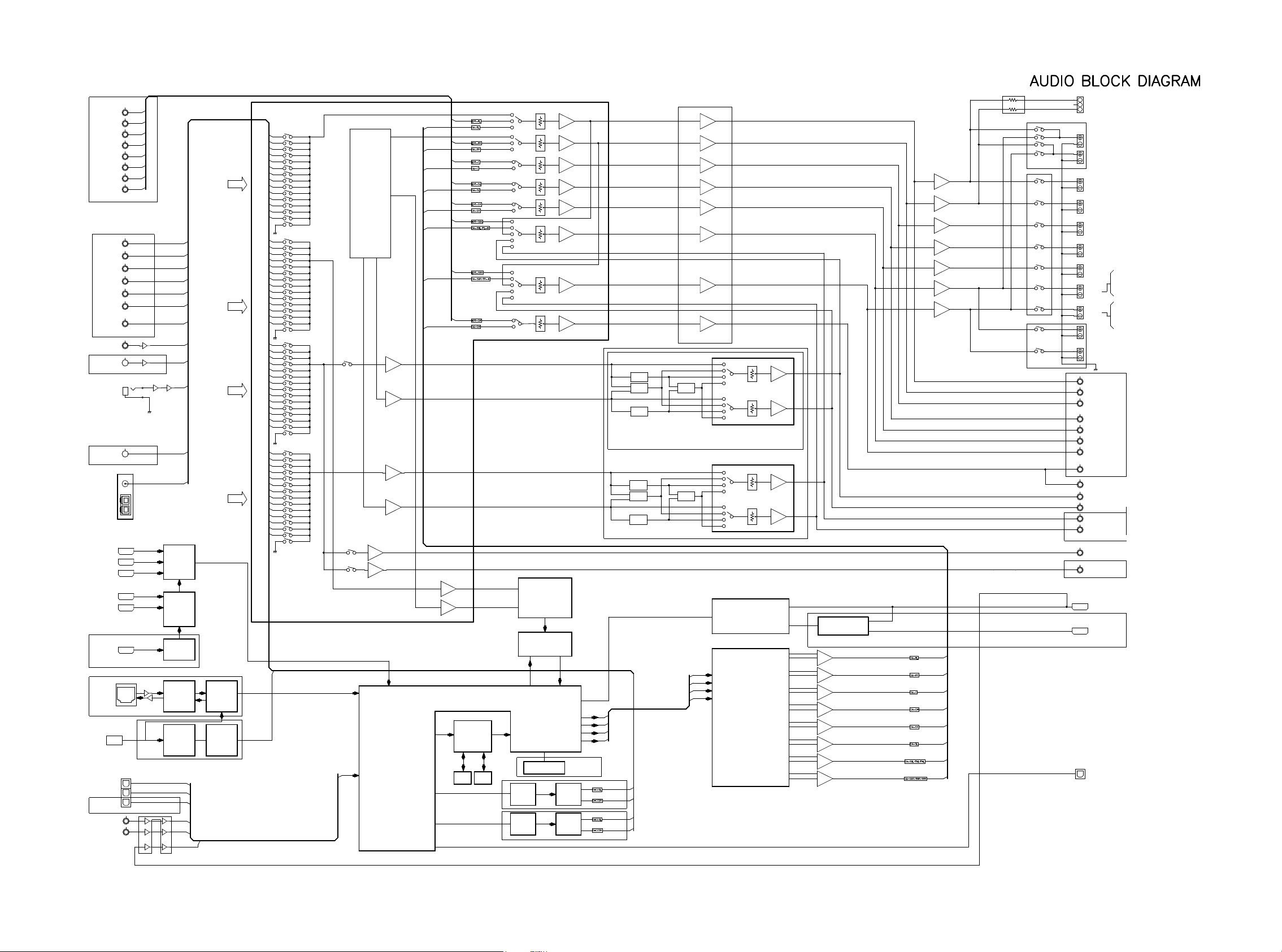
66
C
FR
FL
I2S
SL
SR
SPDIF
OPT2
OPT1
ZONE3
ZONE2
TO DSP
DIRECT
SPDIF
SPDIF
SPDIF
DIR2
LC89058
I2S
HPF
HPF
HPF
HPF
SPDIF/I2S/DSD
+
-
ATT
Z3R
Z3L
Z2R
Z2L
SW1
SBR
SBL
SR
SL
FL
SR
SL
FL-B/FL-H
M-XPort
SIRIUS
SR6005/SR7005
FRONT
HDMI
HDMI5
HDMI4
HDMI3
HDMI2
HDMI1
USB
CONTROLLER
TCC8600
ETHERNET
PHY
LAN8700
TMDS
BUFFER
HDMI
SWITCHER
ADV3002
HDMI
RECEIVER
ADV7840
SPDIF
FLASH
SDRAM
DSP
ADSP21367
DIR3
LC89058
ZONE2
DAC
AK4424ET
I2S
SR7005
+
-
+
-
+
-
+
-
+
-
+
-
HDMI OUT2
HDMI OUT1
C
FR
SBL
SBR
C
FR-A
FL-A
FR-B/FR-H
REC OUT
HDMI IN
FRONT
INPUT
7.1CH
INPUT
R-CH
Audio
Selction
ZONE3
DAC
AK4424ET
+
-
COAX2
SR6005
SR7005
SR7005
SR7005
SR5005 N model & Other
/7005 N model & Other
SR5005/7005 U model
HD-RADIO
SR5005/7005
SW
SR6005,SR7005
SR7005
SR7005
MONO
MIX
MONO
MIX
MONO
MIX
MONO
MIX
PI3HDMI1310A
HDMI
TRANSMITTER
SR6005/7005
RELAY BLOCK
SR6005/7005
SR7005
SR6005/7005=7.2CH
COAX1
FRONT
OPT
DIGITAL IN
USB FRONT
ETHERNET
AM/FM TUNER
SR7005=7INPUT
ANALOG
INPUT
SBL
SBR
DAC
AK4424ET
NETWORK
CONTROLLER
DM860
SPDIF
I2S/SPDIF/DSD
VOLUME AND INPUT SELECTOR
R2A15220FP
AUDIO PLD
EPM240T100C5N
SR7005
DIR1
LC89058
ADC
AK5358B
MAIN ZONE DAC
AK4358VQ
(PCM ONLY)
HDMI SWITCHER
ADV7511
ZONE3 VOLUME
NJW1194
ARC SPDIF
FWR
FWL
HDMI OUT
PRE-OUT
SPK OUT
HEADPHONE OUT
CURRENT
FEEDBACK AMP
MIC(Mini Jack)
HD Radio
CLOCK JITTER
REDUCER CS2100
ZONE2 VOLUME
NJW1194
DIGITAL OUT
SR6005
SBR/Z2R
SR7005
SBR/Z2R/Z3R
SR6005
SBL/Z2L
SR7005
SBL/Z2L/Z3L
TC74HCU04AF
SR6005/7005 U model
SR7005
SR7005
SR7005
SW2
IC1003 (8U-210105)
U1100
(8U-310051)
U1002
(8U-310051)
U4202
(8U-310051)
U0001
(8U-310051)
U3900
(8U-310051)
U3000 (8U-310051)
U3200
(8U-310051)
U2805 (8U-310051)
U3802 (8U-310051)
U1801 (8U-310051)
U1803 (8U-310051)
IC3011 (8U-210105)
IC3007 (8U-210105)
BLOCK DIAGRAM
Page 67

67
Y
Cb
Y
75
24
2V
2V
2V
2V
2V
75
75
Y
Cb
Cr
Cb
Cr
Cr
Y
Cb
75
75
75
2V
2V
2V
2V
2V
Y
75
75
75
75
Cr
2V
2V
C
COMP4-Cr
UP-Cr
COMP1-Cr
COMP2-Cr
UP-Cb
UP-Y
COMP3-Y
COMP2-Y
24
51
75
AVDM-2000
2V
2V
1K
75
75
75
75
75
75
2V
75
75
75
75
Cb
VCR
BD
DVD
Y
IN4
IN3
IN1
HDMI6
HDMI4
HDMI2
2.2K
2.2K
MAIN Y/C
ZONE2 Y/C
COMP3-Cr
COMP4-Y
COMP1-Y
51
75
51
75
2V
2V
75
1K
75
1K
DET.
1K
1K
75
75
DET.
OSD
75
75
68
82
OSD V
75
75
82
75
82
Cb Cr
Cr
Y
Cr
Y
Cb
IN2
HDMI1
HDMI3
HDMI5
FRONT
HDMI
TC4052
75
0dB
SR6005/7005
COMP4-Cr
COMP4-Cb
SR6005 ONLY
COMP2-Y
COMP1-Cr
COMP1-Cb
SPDIF/I2S/DSD
Y/C MIX
COMP2-Cb
COMP3-Cb
COMPONENT & CVBS SELECT
24
SR5005
FROM RX DIGITAL AUDIO
FROM DIGITAL AUDIO
2V
2V
AUX
ETHERNET
COMPONENT IN
HDMI IN
SR7005
SR7005 ONLY
COMP3-Cb
COMP3-Cr
COMP2-Cr
COMP3-Y
COMP2-Cb
COMP1-Y
SR7005
SR6005
SPDIF/I2S/DSD
OSD V
COMP1-Cb
COMP4-Cb
DDRII 512 400MHz
U2500(8U-310051) U2501(8U-310051)
8MBit*16Bit*4Bank
I/P SCALER
IP SCALER
U2200
(8U-310051)
ABT2015
DC CLAMP
OSD
LC74781
SR5005
TO DIGITAL AUDIO
SR7005
2V
HDMI BUS
BUFFER
CVBS REC OUT
CVBS MAIN OUT
COMPONENT
Z2 MONI. OUT
COMPONENT
OUT
HDMI OUT2
HDMI OUT1
CVBS IN
SAT
COMP4-Y
TMDS SW
U1012
(8U-310051)
ADV3002
HDMI Rx
U1100(8U-310051)
VIDEO DECODER
ADV7840
BUS SW FPGA
U1601(8U-310051)
U1801(8U-310051)
U1800(8U-310051)
U2001(8U-310051)
U2003(8U-110085)
U1002(8U-110085)
U1803
(8U-310051)
XC35S400A-4FGG320C
NR6005/7005
CVBS Z2
MONI. OUT
SR7005 ONLY
SR7005
INPUT SELECT
U2001(8U-110085)
DDRII 512 400MHz
8MBit*16Bit*4Bank
TO DIGITAL AUDIO
HDMI
TRANSMITTER
ADV7511
HDMI
Tx AUDIO BUS SW
TC74VHC244FT
ENCODER
ADV7392
Page 68

68
S5(-VKK)
5.2V
DV3.3V
DV3.3V
NET3.3V
FL AC (F2)
A.V-5.0V
A.V+5.0V
MAIN -B
3
4 1
2
VCC
DV1.0V
NET1.2V
DA1.2V
CEC1.8V
NET1.8V
DV1.8V
CEC3.3V
DA3.3V
ABT2015
ADSP21367
ADV7840
DM860(SR7005)
TCC8600(SR6005)
DV 5V
FL AC (F1)
DA+5.0V
A-8.0V (Pre)
A+8.0V (Pre)
MAIN +B
CPU POWER
MAIN PWR ON
S4(VIDEO)
S1(AMP +B)
CEC3.3V
DV 5V
VE 1.8V ADV7392
VH
A.V+3.3V
SCPU+5V
CEC+5V
USB+5V
REMOTE POWER
SWM3.3V
M3.3V
BD7128*3,BU4052*1,AVDM2000
AVDM2000
BU7628*3,BU4052*1
AC CORD
S6(FILAMENT)
S2(+8V,-8V)
PQ018DNA
PQ012ENB
PQ018ENA
PQ033DNA
PQ033DNA
NJM2388F
PQ120
NJM7908
NJM7805
AVDD 1.8V ADV7840
GUI 1.2V XC3S400A
VE 3.3V ADV7392
TC74VHCT125,PI3HDMI1310
SCPU+3.3V
BFNK0563F5R
A
ND330Q
P
MUTE3.3V
REMOTE3.3V
SWM5V
AZ4580*15,R2A15220,NJW1194*2
AK5358/AK4424*2
AZ4580*15,R2A15220,NJW1194*2
NJM7905
NJM7805
PQ120
BA08T
PQ033DNA
TC74VHCT244,ADV7511,PI3HDMI1310,ADV7392
ADSP21367,W9864G,EN29LV160BB
SAA7121,LAN8700,DM860
TC74VHC08,MC14094BD*4
R5F64169DFD,EN29LV160BB
2388F09 : TUNER(N,F,K model) +9.0V
D1.0V
DV POWER3
D1.2V1
NET POWER
ABT2015,ADV7511,K4T51163QG*2
ADV7840,ADV3002,AD8195
CS2100,EPM240T,LC89057*3,TC74VHCU04
M25P40,TC74VHCT125*3,XC3S400A,ABT2015
MAIN TRANS
ILX3232D,TC74VHCT125VF
TC74VHCT08,MC14094BD
TRIGGER +12V
TRIGGER +12V
VCC DIAGRAM
D1.8V
D5V POWER
D1.2V2
DA POWER
D3.3V1
D5V POWER
D3.3V2
D5V POWER
Page 69

69
F$
F$
ޓF$
F$
F$
F$
F$
F$
F$
F$
F$
F$
F$
.+0'+0%*+0
F$(5
F$(58TOU
F$(5
F$(5
F$(5
#-83
#-$
*2176
LEVEL DIAGRAM
FRONT ch
F$
F$
F$(58TOU
F$(5
F$(5O8TOU
F$(5
F$(5
O8
F$
52-176
F$
(7..5%#.'.'8'.8TOU
%QPHKI.550&1.$;.+/+6.'8'.8TOUEJF$(5CV*\
F$
)#+0UGVVKPIQH/#56'481.F$
㨯59;'5&+)+6#.ޓޓF$F$F$F$F$
㨯59;'5#0#.1)ޓޓF$F$F$F$F$
㨯59010'&+)+6#.ޓޓF$F$F$F$F$F$
㨯59010'#0#.1)ޓޓF$F$F$F$F$F$
㨯&+4'%6QT%*+0ޓF$F$F$
#0#.1)ԘԙԚԛԜԝ
Ԙ$CUKE1((5'6QH81.F$KPFKECVKQPXCNWG
ԙ(4106EJTGXKUKQP
Ԛ1((5'6QH59010'
ԛ1((5'6QHVJG#&KPRWV
Ԝ4GXKUKQP1((5'6QHVJG&+)+6#.KPRWV
ԝ0GICVGVJGICKPQHEWTTGPVHGGFDCEMCORNKHKGTU1((5'6
F$
F$
5901
F$(5&+)+0
F$(5#&+0
F$(5&+)+0
F$(5#&+0
㧗
㧗
.+0'+0
%*+0
*2176
61
<10'
㧗
52'#-'4
176
&52
#0#.1)
#66
4#(2
4'%176
)#+0
#&,
24'176/76'
61
<10'
4'%176
#-83
&#
㧙
㧙
㧗
2.&
#-$
#&
F$
F$(5
O8TOU
24'176
O8TOU
O8TOUǡ
8TOUǡ
F$
O8TOU
.2()#+0F$
O8TOU
F$
O8TOU
F$
O8TOU
O8TOU
#&+0O8TOU
F$
*GCFTQQOF$
F$
%744'06
(''&$#%-
#/2
219'4
#/2
F$
F$
O8TOU
F$
LEVEL DIAGRAM
s
s
Page 70

70
F$
F$
ޓF$
F$
F$
F$
F$
F$
F$
F$
F$
F$
F$
%*+0
LEVEL DIAGRAM
CENTER ch
F$(5
F$(5
F$(5
O8
F$
52176
F$
/#:5+)0#..'8'.
F$
㧗
%*+0
㧗
52'#-'4
176
&52
4#(2
)#+0
#&,
24'176/76'
#-83
&#
㧙
㧙
㧗
2.&
F$(58TOU
F$(5O8TOU
O8TOU
.2()#+0F$
F$
F$
O8TOU
F$
#0#+0276O8TOU.4M*\
/1&'/7.6+%*56'4'1
O8TOU
)#+0UGVVKPIQH/#56'481.F$
㨯&1.$;&+)+6#.+0F$F$F$F$
㨯#0#.1)+0ޓޓF$F$F$F$
㨯%*+0ޓޓF$F$F$
ԘԙԚԛ
Ԙ$CUKE1((5'6QH81.F$KPFKECVKQPXCNWG
ԙ1((5'6QHVJG#&KPRWV
Ԛ4GXKUKQP1((5'6QHVJG&+)+6#.KPRWV
ԛ0GICVGVJGICKPQHEWTTGPVHGGFDCEMCORNKHKGTU1((5'6
O8TOU
24'176
O8TOU
8TOUǡ
%744'06
(''&$#%-
#/2
219'4
#/2
&&+0276F$(5%06M*\
O8TOU
F$
F$
s
Page 71

71
F$
F$
ޓF$
F$
F$
F$
F$
F$
F$
ޓO8TOU
F$
F$
F$
F$
LEVEL DIAGRAM
SUBWOOFER ch
F$(5
F$(5O8TOU
F$(5O8
F$(5
O8
F$
59EJ&#%/#:5+)0#..'8'.
&&+0276F$(5.('*\
24'176
㧗
%*+0
&52
4#(2
)#+0
#&,
24'176/76'
#-83
&#
㧙
㧙
㧗
2.&
F$(58TOU
O8TOU
F$
O8TOU
F$
&&+0276F$(5.('*\
%QPHKI555;&1.$;.+/+6.'8'.8TOUEJF$(5CV*\
8TOU
)#+0UGVVKPIQH/#56'481.F$
㨯&1.$;&+)+6#.+0F$F$F$F$F$
㨯#0#.1)+0F$F$F$F$F$
㨯%*+0F$F$F$F$
ԘԙԚԛԜԝ
Ԙ$CUKE1((5'6QH81.F$KPFKECVKQPXCNWG
ԙ57$911('4EJTGXKUKQP
Ԛ1((5'6QHVJG#&KPRWV
ԛ4GXKUKQP1((5'6QHVJG&+)+6#.KPRWV
Ԝ+PKVKCNXCNWGQH%*+059.GXGN
ԝ0GICVGVJGICKPQHEWTTGPVHGGFDCEMCORNKHKGTU1((5'6
.2()#+0F$
F$
F$
O8TOU
24'176
F$
#-83
O8TOU
F$
ޓO8TOU
#0#+0276O8TOU.4*\
O8TOU
F$
%*+0
%744'06
(''&$#%-
#/2
F$
F$
F$
O8TOU
F$
s
Page 72

72
F$
F$
ޓF$
F$
F$
F$
F$
F$
F$
F$
F$
F$
F$
%*+0
LEVEL DIAGRAM
SURROUND ch
F$(5
F$(5O8TOU
F$(5
O8
F$
F$
/#:5+)0#..'8'.
F$
㧗
%*+0
㧗
52'#-'4
176
&52
4#(2
)#+0
#&,
24'176/76'
#-83
&#
㧙
㧙
㧗
2.&
#-83
F$(58TOU
F$(5O8TOU
&&+0276F$(55744M*\
O8TOU
#0#+0276O8TOU.4M*\
/1&'/7.6+%*56'4'1
.2()#+0F$
F$
F$
O8TOU
O8TOU
F$
F$
)#+0UGVVKPIQH/#56'481.F$
㨯&1.$;&+)+6#.+0F$F$F$F$
㨯#0#.1)+0ޓޓF$F$F$F$F$
㨯%*+0ޓޓF$F$F$
ԘԙԚԛԜ
Ԙ$CUKE1((5'6QH81.F$KPFKECVKQPXCNWG
ԙ1((5'6QHVJG#&KPRWV
Ԛ4GXKUKQP1((5'6QHVJG&+)+6#.KPRWV
ԛ4GXKUKQP1((5'6HQT5.54KP/7.6+%*56'4'1
Ԝ0GICVGVJGICKPQHEWTTGPVHGGFDCEMCORNKHKGTU1((5'6
24'176
O8TOU
O8TOU
8TOUǡ
52176
%744'06
(''&$#%-
#/2
219'4
#/2
F$
O8TOU
8TOUǡ
F$
O8TOU
F$
F$
s
Page 73

73
F$
F$
ޓF$
F$
F$
F$
F$
F$
F$
F$
F$
F$
F$
%*+0
LEVEL DIAGRAM
SURR.BACK ch
F$(5
F$(5
O8
F$
52176
F$
F$
㧗
%*+0
㧗
52'#-'4
176
&52
4#(2
)#+0
#&,
24'176/76'
#-83
&#
㧙
㧙
㧗
2.&
HTQO
<10'
HTQO
<10'
HTQO
<10'
&&+0276F$(55.54M*\
5$/64:10&&':/1&'
#0#+0276O8TOU.4M*\
/1&'/7.6+%*56'4'1
#-83
F$(5O8TOU
F$(58TOU F$
.2()#+0F$
O8TOU
)#+0UGVVKPIQH/#56'481.F$
㨯&1.$;&+)+6#.+0F$F$F$F$F$
㨯#0#.1)+0ޓޓF$F$F$F$F$F$
㨯%*+0ޓޓF$F$F$
ԘԙԚԛԜԝ
Ԙ$CUKE1((5'6QH81.F$KPFKECVKQPXCNWG
ԙ5744$#%-EJTGXKUKQP
Ԛ1((5'6QHVJG#&KPRWV
ԛ4GXKUKQP1((5'6HQT5$.5$4KP/7.6+%*56'4'1
Ԝ4GXKUKQP1((5'6QHVJG&+)+6#.KPRWV
ԝ0GICVGVJGICKPQHEWTTGPVHGGFDCEMCORNKHKGTU1((5'6
O8TOU
F$(5O8TOU F$
F$
F$
/#:5+)0#..'8'.
8TOUǡ
O8TOU
24'176
O8TOU
%744'06
(''&$#%-
#/2
219'4
#/2
F$
O8TOU
8TOUǡ
F$
F$
F$
O8TOU
s
Page 74

74
.+0'+0
F$
F$
ޓF$
F$
F$
F$
F$
F$
F$
ޓF$
F$
F$
F$
F$
.+0'+0
F$(5
8TOU
24'176
F$
F$(5
F$(5
F$(5
F$(5
F$(5
F$(5&+)+0
#-'6
O8
/#:5+)0#..'8'.8TOU
52'#-'4
176
<10'
24'176
/76'
F$
52176
/101
*2(
&#
HTQO
$EJ
61
/#+0
<10'
5$EJ
(4106<10'CUUKIPF$
/101
*2(
/101
610'
&#
<10'
24'176
/76'
<10'0,9
<10'0,9
HTQO
(EJ
610'
HTQO
%*+0
5$EJ
/101
4#(2
LEVEL DIAGRAM
ZONE2/3
F$
8TOUǡ
O8TOU
㧗
%744'06
(''&$#%-
#/2
219'4
#/2
F$F$
s
Page 75

75
Pb
R420
J419
R415
J409
J408
CN404
Q402
R427
R411
J585
C408
J411
J413
R416
Q411
C411
R703
R413
R441
Q412
C414
J416
R443
J401
R430
J518
R419
R552
R545
J445
R541
R567
R534
R566
R554
J438
C457
J436
R546
J439
Q447
R543
Q448
C462
J442
R540
R561
J444
J443
R507
R498
R524
R489
R522
ZD409
R511
C441
J455 J465
Q435
J429
C467
C446
J468
J467
R497
R530
R517
J474
R593
J508
J486
R600
C465
J511
J560
R595
R609
C476
R608
J499
R598
J431
C472
J456
D428
J489
J491
J559
J492
R582
J493
R583
C483
R603
J495
J496
R463
R465
C417
R455
J525
R467
J516
C424
J515
J517
D408
R456
J526
R452
R477
J519
R453
C499
R474
J521
J522
R636
R638
C481
J549
R643
J551
R640
J542
R508
C488
J541
J543
D432
R629
J552
R625
R655
R649
C518
J547
R659
R647
CP405
C497
J575
R671
J565
Q474
R686
J577
R683
J568
J566
R684 J567
J569
D438
R668
R698
R692
R709
R700
J574
J572
R702
R690
C412
J404
J410
Q408
R401
D405
J415
J418
J457
J434
J446
J432
R531
R716
R570
J427
J441
D424
J534
R549
J428
R523
R499
J460
J472
R506
R527
R712
R488
R705
D417
J469
J498
R715
D426
R589
R606
R575
J570
Q455
D430
J500
R592
J464
J461
J524
J513
J514
ZD406
R711
R446
Q419
D411
D412
J544
R457
J480
J533
J550
R653
C496
ZD418
J536
R617
R714
R618
J545
J558
R630
D435
D436
R679
J482
J576
R696
C512
J578
R661
J557
D441
R673
R536
J424
D404
C409
D401
R438
R717
R434
R442
R440
J453
J403
R538
J454
R560
J450
D422
R533
ZD410
R720
R568
R572
C454
R564
R558
J561
R492
R495
J476
R519
J483
R520
Q425
J458
R529
R585
R577
R605
ZD414
J528
D410
R447
J510
R482
R718
C422
R478
R471
J554
J466
R648
D434
D433
R619
R654
R722
R658
R644
R664
R681
J590
J580
J481
R691
D440
D439
ZD419
J562
R701
R694
R687
R551
Q417
C402
R425
J421
R435
R424
R412
C517
J412
D402
C515
J422
J406
R403
C404
R429
C406
C435
R409
R418
R404
R428
R436
J426
C449
R439
C407
R431
R433
R550
R542
TP401
R410
R535
Q438
VR404
R557
J451
R569
J449
R565
ZD412
J447
D421
ZD411
R555
C459
R563
D420
J448
R706
D419
R548
R559
C452
Q437
R571
C451
R539
C456
J471
C433
R502
R562
J473
J462
R573
D423
TP404
R509
Q426
VR403
C444
C440
R514
J477
J475
R526
R512
C439
ZD408
D415
D416
J463
R503
D414
J537
C443
J430
R528
Q436
R496
ZD407
J583
R515
R588
R597
J497
ZD415
R518
J488
J487
R581
C468
Q450
D425
R576
R578
R602
VR405
C470
R610
J504
C478
R612
C471
J501
R604
J485
R616
Q459
D429
R614
R615
Q449
Q460
R574
TP405
R458
R468
J523
R479
R454
J588
J587
R459
C425
R473
R451
R445
ZD404
C420
D407
Q423
VR402
C428
R481
R461
R480
J530
C430
R631
R483
C423
R475
C427
J520
R704
CP403
R487
R485
TP402
J555
J553
ZD417
R641
R651
C491
R632
ZD416
R708
C489
J540
R627
R628
C484
R620
D431
R645
Q471
R634
Q472
C486
R650
R652
C494
R674
R646
R670
J548
R678
J546
J563
R667
R663
R626
VR407
TP406
R695
J581
J579
ZD420
C510
C503
R693
C505
C507
J571
R672
R675
Q484
Q473
C519
R669
R677
Q483
R689
BAR CODE
IN OP FIADJICT
J435
C416
J405
R710
C410
J420
ZD403
R421
R437
Q407
C415
R402
D406
J417
R414
J440
C458
R532
Q444
Q443
J437
C464
R544
J535
J506
J407
C448
D418
Q432
R490
Q431
J490
R584
C480
J470
C473
C475
C479
J539
J494
R613
Q456
R707
J479
C432
C426
J512
C513
Q420
C431
J505
J532
R444
R484
J538
J589
C490
R656
Q468
C495
R635
J531
J591
J564
R660
ZD421
R713
R699
Q480
Q479
TP407
D442
J509
J433
R432
D403
J584
ZD401
R405
Q401
R422
J502
J507
R491
J484
R448
R611
R721
R525
R719
C438
R521
R607
R601
J459
R476
D409
R662
R462
Q461
R621
Q413
R723
R624
R697
R486
C502
R472
J425
J452
J423
ZD402
C455
J402
C516
R408
VR401
C460
J478
J503
D427
C447
CP402
R505
R591
R516
Q414
ZD413
C436
D413
CP401
J529
J556
ZD405
C487
J527
D437
C500
Q462
R688
Q424
R657
C492
C508
VR406
C504
J582
R493
J573
C419
C514
C463
C442
C474
TP403
C506
Q467
C511
BCE
C
MTZ5.1A
C E
CECEB
C
E
CE
FL
SL
E
C
SR
C
B
FR
BE
CE E B
BE
EE B
BE
BE
G401
E
WIRE
B
C/SBDIP
SBL
NC
SBR
B E
G402
G401
E B
BONDING
WIRE
BC
AGND
MTZ5.1A
AGND
SBL
AGND
SBR
AGND
BONDING
WIRE
MTZ5.1A
WIRE
ASO DET
RADI THERMAL
BE
B
B
BKT400
MTG
B
MTZ5.1A
B
C
C
B
C
C
FR
C
FL
MTZ5.1A
CB
C
MTZ5.1A
C
HIGHGND
HIGHGND
PREGND
-HIGHB
+HIGHB
+HIGHB
+HIGHB
-HIGHB
BONDING
WIRE
C
C
BONDING
G400
WIRE
BONDING
G400
C
EC
BONDING
G402
CLAMP 401
BONDING
C
WIRE
E
100/100
TR THERMAL
DC DET3
DC DET4
FL
AGND
AGND
SR
SL
SR
HIGHGND
-HIGHB
WIRE
FR
MTZ5.1A
WIRE
BONDING
SBL
WIRE
WIRE
BONDING
BONDING
CLAMP 400
SL
BONDING
SBR
7020-06941-000-0S
7CH AMP B'D
631010096006S
181716151413121110987654321
F
E
D
C
B
A
7CH-AMP (COMPONENT SIDE)
鉛フリー半田
半田付けには、鉛フリー半田 (Sn-Ag-Cu) を使用してください。
Lead-free Solder
When soldering, use the Lead-free Solder (Sn-Ag-Cu).
WIRE
WIRE
WIRE
E
BC
E
C
E
B
CE
B
C
E
E
B
C
B
EBC
E
E
B
C
B
EC
E
E
B
C
C
B
E
C
E
E
B
C
B
E
C
B
E
E
B
C
B
E
C
B
E
WIRE
C
B
C
WIRE
WIRE
WIRE
WIRE
B
C
C
B
B
C
WIRE
CE
B
R407
C403
Q405
Q439
Q430
R510
R500
R734
Q454
R729
R730
C401
R406
R732
D444
Q406
C413
R537
R727
R464
R733
J592
C469
R587
C421
C485
C501
D443
R423
D449
Q442
C461
R590
R466
R639
C493
C509
R426
Q403
R724
C450
R553
R556
Q427
R513
R504
R501
Q451
D457
R469
R725
R633
R642
Q463Q475
R685
R676
R731
C405
D450
C453
R494
C434
R726
D448
C437
R580
C466
D458
D452
R596
R586
R450
C418
Q418
D446
C482
R623
Q466
D454
R666
C498
Q478
D456
Pb
R547
D447
C445
D451
C477
Q415
D445
C429
D453
R682
D455
R417
R460
R728
R599
R449
123456789101112131415161718
F
E
D
C
B
A
7CH-AMP (FOIL SIDE)
PRINTED WIRING BOARDS
Page 76

76
鉛フリー半田
半田付けには、鉛フリー半田 (Sn-Ag-Cu) を使用してください。
Lead-free Solder
When soldering, use the Lead-free Solder (Sn-Ag-Cu).
SMPS (COMPONENT SIDE) SPK WIDE (COMPONENT SIDE)
MTG
MTG
JK100
BONDING
F100
DGND
DGND
MTZJ22B
PC123
MTG
F101
D5.2V
D5.2V
BONDING
BONDING
BONDING
MTZJ22B
ST-4430A
BKT101
T6.3AL/250V
T2AL/250V
BKT100
NEUTRAL
LIVE
470P/250V
470P/250V
0.1UF/250V
MTZJ5.6B
LF4ZBE273H
MTZJ22B
MTZJ22B
MTZJ22B
5600UF/6.3V
5600UF/6.3V
100UF/400V
BONDING
1000P/1KV
MTZJ22B
BONDING
D25SC6M
MTZJ39B
MTZJ39B
TOP258MG
MTZJ22B
MTZJ39B
MTZJ39B
2200P/250V
Pri.
Sec.
BONDING
BKT102
7020-06942-101-0S
MAINPOWER
SMPS B'D
LF4ZBE273H
MTZJ22B
0.01UF/250V
BONDING
5600UF/6.3V
0.1UF/250V
5600UF/6.3V
Sec.
D112
J154
J153
J158
J157
J177
J155
C114D111
D110
J171
TR102
J176
CX104
J178
ZD114
J179
J152
ZD117
ZD107
D101
D102
ZD100
ZD118D108
ZD101ZD105
ZD119
J161
CX100
CX102
CX106
J180
C100
C117
CX103
CX105
C101
J151
ZD104
ZD102
L101
J168
D106
R113
D104
D105
D100
J175
J156
J159
ZD108ZD109ZD110
TR101
R105
D109
ZD112
R119
R110R112IC116
R104
R122
ZD113
Pb
ZD116
C119
J164
C104
C105
RL101
TH100
J169
ZD106
J170
C107
C108
C103
IC102
J160
C115
BAR CODE
ZD103
R111
J165
L100
R100
R115
ZD111
R101
TR100
IN OP FIADJICT
C102
ZD115
C112
D103
R107
C106
IC100
T100
C109
121110987654321
F
E
D
C
B
A
DGND
E
C
CA A
Pri.
Sec.
D5.2V
Sec.
MAINPOWER
C125
C118
R121
R109
C124
C113
R125
R118
C122
C121
C120
R124
C111
C110
R114
R120
R123
R126
R144
R108
R106
C123
C116
123456789101112
F
E
D
C
B
A
SPK WIDE (FOIL SIDE)
54321
CP13
FR_WIDE
F-WIDEV
FR_W_GND
RLGND
FL_W_GND
7020-06942-301-0S
FRONT WIDE SPK
JACK5
FL_WIDE
C85
RLY8
Pb
C84
JACK4
A
B
C
D
E
54321
A
C88
C86
C87
B
C56
C
C89
C90
C91
D
C59
E
Page 77
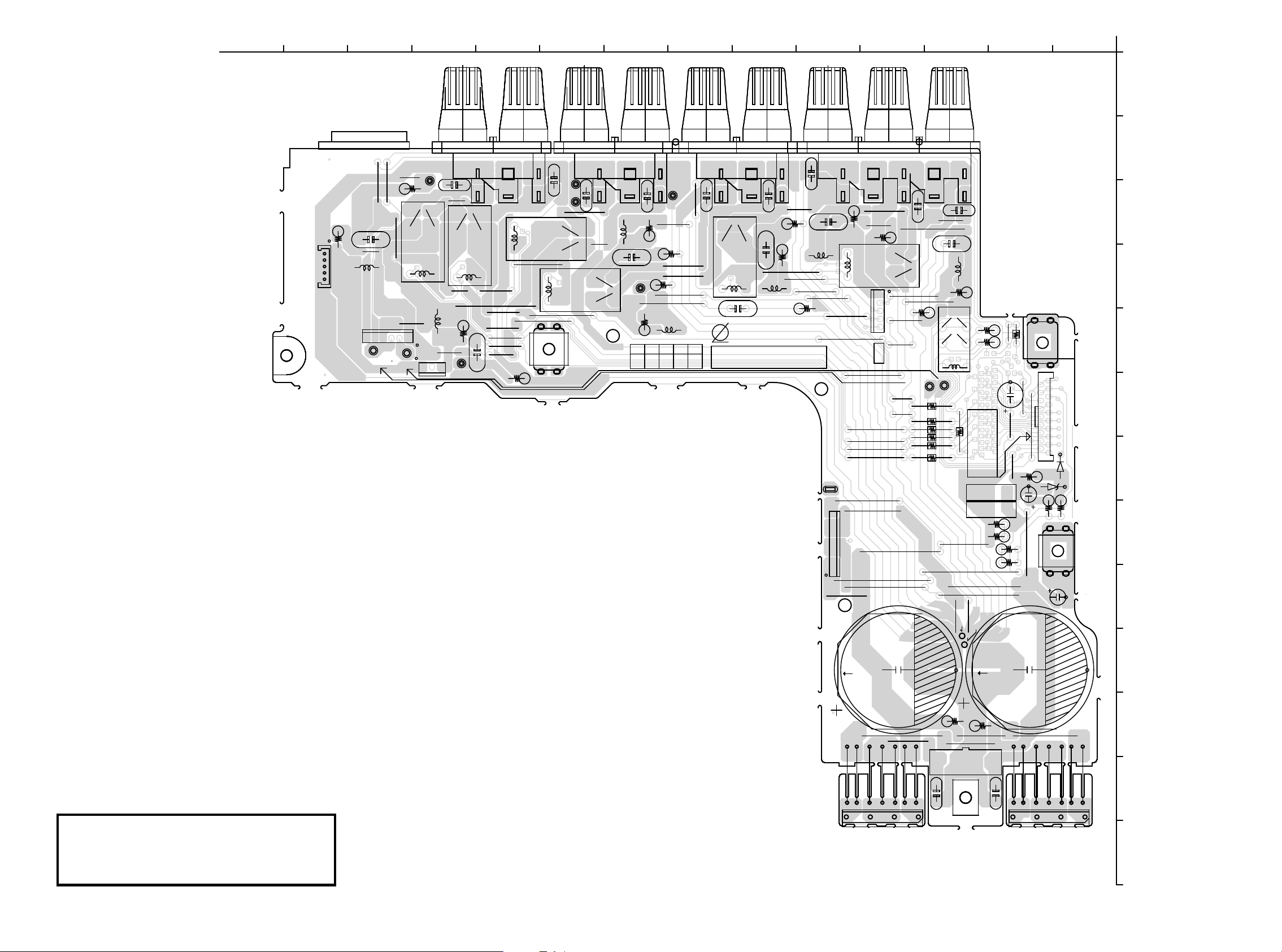
77
鉛フリー半田
半田付けには、鉛フリー半田 (Sn-Ag-Cu) を使用してください。
Lead-free Solder
When soldering, use the Lead-free Solder (Sn-Ag-Cu).
SPK (COMPONENT SIDE)
BLACK(L)
WIRE3
WIRE5
+HIGHB
+HIGHB
+HIGHB
-HIGHB
-HIGHB
-HIGHB
PREGND
HIGHGND
HIGHGND
SL
FR
FL
WIRE1
WIRE5
WIRE5
H/PL
H/PR
2
18
BKT1
FL_WIDE
FL_W_GND
FR_W_GND
FR_WIDE
F-WIDEV
RLGND
WIRE2
SBL
WIRE4
BKT3
HIGHGND
D3SB60
SR
RL+B
NC
BONDING
D3SB60
WHITE(R)
WIRE5
WIRE3
CLAMP3
CEN
0.1-J/5W
RELAY_H
H/PGND
RELAY_F
RELAY_C
RELAY_S
RELAY_SB
LIMITLIMIT+
LIMIT+
MUTE+7V
RLGND
WIRE2
1
19
WIRE1
SBR
WIRE4
BONDING
RELAY_FB
RELAY_H/P
BLACK(L)WHITE(R)
LIMIT-
BKT2
SPK B'D
7020-06942-201-0S
RELAY_WIDE
J38
J75
J80
C11
J11
J5
J4
J13
C3
C61
J10
J32
J74
J15
J7
D8
L7
L4
J2
J85
R53
R28
J46
J87
J33
L5
J51
J65
J56
J77
R35
J42
R24
R22
R21
R20
J89
J79
J18
R29
R34
L6
CP22
CN2
C25
J24
C21
J35
J50
C24
C16
C12
R12
R39
C19
J34
R5
L1
C17
C14
J12
J6
J96
J73
C8
C54
J3
R23
R25
R9
L3
C9
R10
J78
C6
J8
J9
J16
J14
C60
R32
C57
DZ1
C22
J82
R15
R17
RLY6
R11
R13
C1
Pb
CN3
R7
CN1
C4
J1
RLY1
R19
J31
R31
J43
CP12
J76
J84
J88
R18
J21
J22
J27
J52
J58
J54
J70
J68
L2
R6
J55
J20
J19
J28
J17
J29
J66
J36
R30
R26
J69
J97
R38
J71
J81
CN13
R16
J25
BAR CODE
IN OP FIADJICT
J26
J49
RLY4
J40
J53
J57
R14
J39
CP1
R33
J86
R27
C53
J62
R37
R8
J72
RLY7
RLY5
RLY3
R36
C58
AC AC
+
D10
JACK2
J45
J83
J92
J93
J91
J63
J23
J44
J94
J37
RLY2
C55
AC AC
+
-
D9
JACK1
JACK3
1413121110987654321
M
L
K
J
I
H
G
F
E
D
C
B
A
Page 78
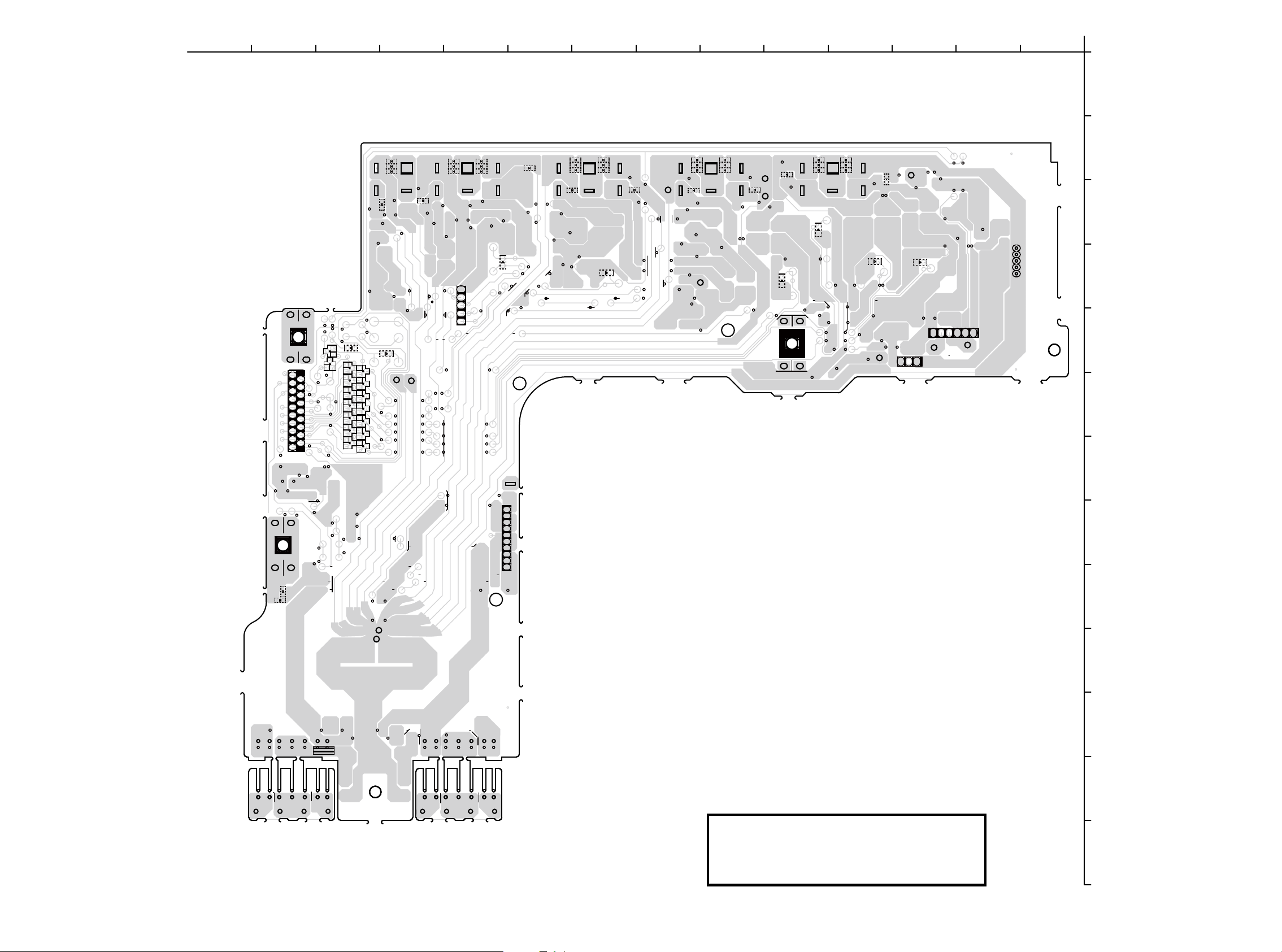
78
鉛フリー半田
半田付けには、鉛フリー半田 (Sn-Ag-Cu) を使用してください。
Lead-free Solder
When soldering, use the Lead-free Solder (Sn-Ag-Cu).
SPK (FOIL SIDE)
C2
Q9
C20
C18
C10
C13
C31
C30
C29
Q8
C62
D5
C15
C23
D3
C7
Q6
Q4Q2
C63
Q21
D7
D6
C48
C47
C49
D4
C50
C51
C52
C41
C42
C43
C46
C45
C44
C37
C36
C35
C40
C39
C38
D2
C34
C33
C32
C28
C27
C26
Q1
Q7
D1
Q3 Q5
C5
Q20
Q14
Q13
Q11
D11
Q10
Q12
M
L
K
J
I
H
G
F
E
D
C
B
A
1234567891011121314
Page 79

79
FRONT_CNT (COMPONENT SIDE)
鉛フリー半田
半田付けには、鉛フリー半田 (Sn-Ag-Cu) を使用してください。
Lead-free Solder
When soldering, use the Lead-free Solder (Sn-Ag-Cu).
REG (COMPONENT SIDE)
s
13121110987659321
H
G
F
E
D
C
B
A
REG_CNT (COMPONENT SIDE)
7654321
F
E
D
C
B
A
RS232C (COMPONENT SIDE)
65421
A
B
C
D
E
F
G
I
J
H
54321
JACK406
C458
ZD402
MTZ16B
C454
C455
CN401
J401
J403
11:NC
10:NC
6:TRG2
7:TRG +15V
9:NC
8:TRG GND
3:232OMI
4:232IMO
5:TRG1
1:REMOTE3.3V
2:D/MGND
A
B
J407
J402
J409
J406
J408
RS232C B'D
Pb
7028-06943-501-0
JACK405
C457
ZD401
MTZ16B
JACK404
J404
J405
J410
C452
C
D
E
Page 80

80
鉛フリー半田
半田付けには、鉛フリー半田 (Sn-Ag-Cu) を使用してください。
Lead-free Solder
When soldering, use the Lead-free Solder (Sn-Ag-Cu).
FRONT_CNT (FOIL SIDE)
12345678910111213
H
G
F
E
D
C
B
A
REG (FOIL SIDE)
s
REG_CNT (FOIL SIDE)
1234567
F
E
D
C
B
A
RS232C (FOIL SIDE)
12345
A
B
C
D
E
G
F
H
I
12345
A
J
IC406
PQ120DNA
5:TRG1
2:D/MGND
3:232OMI
4:232IMO
1:REMOTE3.3V
6:TRG2
7:TRG +15V
9:NC
8:TRG GND
10:NC
11:NC
J437
IC405
PQ120DNA
J438
IC404
ICL3232CVZ-T
R454
R453
C448
D409
C465
C461
C460
C466
C467
C456
C469
C468
B
C
C459
R456
C450
C453
C447
C451
C449
R455
D408
C463
C462
C464
D
E
Page 81
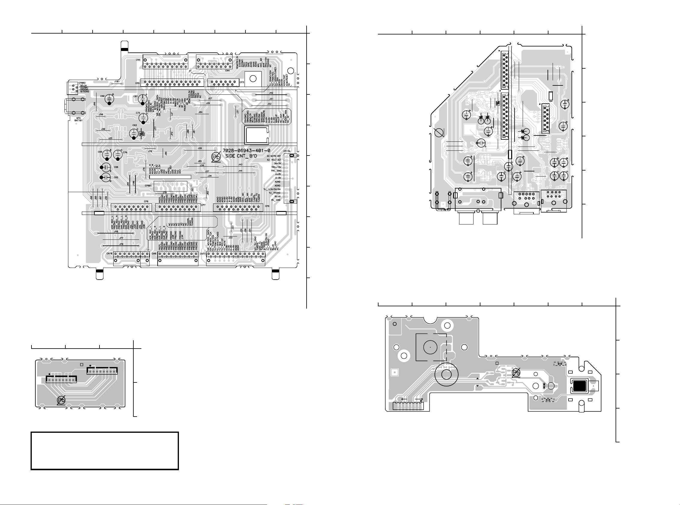
81
鉛フリー半田
半田付けには、鉛フリー半田 (Sn-Ag-Cu) を使用してください。
Lead-free Solder
When soldering, use the Lead-free Solder (Sn-Ag-Cu).
SIDE_CNT (COMPONENT SIDE) SIRIUS (COMPONENT SIDE)
VOLUME (COMPONENT SIDE)
VR CONNECT (COMPONENT SIDE)
181716151413121110
654321
1:NC
2:TRG GND
3:TRG +15V
4:M_XR
5:AGND
6:M_XL
7:AGND
8:SIRIUS_R
9:AGND
J432
J423
R404
R403
JACK403
J421
C429
CN402
R418
J413
CN403
J422
C430
J415
C428
J430
J412
R402
R401
C431
J429
1:REMOTE3.3V
2:D/MGND
3:232OMI
4:232IMO
5:TRG1
J425
6:TRG2
7:TRG +15V
8:TRG GND
J433
J434
J435
JACK401
9:NC
10:NC
11:NC
J417
J426
CP401
J420
J416
J419
J418
C432
C433
JACK402
A
J411
B
C408
C
C407
D
C435
C434
E
A
B
1:RC_IN
2:FRONT IRIN
3:BT_LINK
4:RC_OUT
5:KILLIR
C
D
E
6:WAKEUP
7:A-8V
8:A-8V
9:A+8V
10:A+8V
11:NC
12:SIRIUSRST
C419
13:SIRIUSMI
14:SIRIUSMO
15:D/MGND
16:M3.3V
17:SWM3.3V
18:SWM5V(MX)
19:D5V(MX)
Pb
J431
J428
J427
SIRIUS B'D
7028-06943-601-0
MTG
BKT401
C406
C405
J424
C425
J414
10:SIRIUS_L
11:TRG2
12:TRG1
13:232IMO
14:232OMI
15:REMOTE3.3V
C413
F
F
321
N1004
GND
P.KEY
REDLED
GRNLED
1
GND
M3.3V
ISELB
P.KEY
ISELA
REDLED
GRNLED
SWM3.3V
8U-110100-2
N1003
M3.3V
ISELB
ISELA
SWM3.3V
A
B
G
H
I
7654321
B1001
N1005
ISELB
M3.3V
SWM3.3V
ISELA
15.0
GND
P.KEY
JV47
GRNLED
REDLED
S1026
8U-110100-3
JV116
J1012
J1013
RG
D1001
S1001
ON/STBY
1
7.5
A
B
C
D
Page 82

82
SIDE_CNT (FOIL SIDE) SIRIUS (FOIL SIDE)
VR CONNECT (FOIL SIDE)
VR CONNECT (FOIL SIDE)
123456789
12345
A
1:NC
2:TRG GND
3:TRG +15V
4:M_XR
R405
R438
D401
R425
R434
Q402
C426
C437
5:AGND
6:M_XL
7:AGND
8:SIRIUS_R
9:AGND
10:SIRIUS_L
11:TRG2
12:TRG1
13:232IMO
14:232OMI
15:REMOTE3.3V
Q406
R420
R419
C414
C424
R427
C416
C421
R422
C402
R421
C420
R426
C415
R447
C446
Q401
R414
Q404
R442
R445
R415
C410
IC401
AZ4580
C409
Q405
R433
R410
D402
Q403
R411
C401
C470
C436
C445
R443
R444
IC403
PQ033DNA1ZPH
C441
R407
R406
R452
1:RC_IN
2:FRONT IRIN
3:BT_LINK
4:RC_OUT
5:KILLIR
6:WAKEUP
7:A-8V
8:A-8V
B
R409
R408
R413
1:REMOTE3.3V
2:D/MGND
3:232OMI
4:232IMO
5:TRG1
6:TRG2
7:TRG +15V
8:TRG GND
9:NC
10:NC
11:NC
9:A+8V
10:A+8V
11:NC
12:SIRIUSRST
13:SIRIUSMI
14:SIRIUSMO
15:D/MGND
16:M3.3V
17:SWM3.3V
18:SWM5V(MX)
19:D5V(MX)
C
R412
C403
IC402
AZ4580
C412
C440
D407
C418
R424
C423
R431
R459
D406
R432
R417
R441
C404
C427
C439
R437
D
E
F
R423
R440
R430
D405
R436
R448
D404
D403
C444
R460
R429
C422
R451
C417
C411
R416
C443
R449
C442
R446
R450
R428
C438
R435
R439
A
B
C
D
E
F
N1004
GND
M3.3V
ISELB
ISELA
GRNLED
P.KEY
REDLED
GRNLED
SWM3.3V
N1003
P.KEY
REDLED
GND
ISELA
ISELB
123
M3.3V
SWM3.3V
A
B
G
H
I
1234567
S1001
ON/STBY
R1127
C1002
C1112
Q1003
R1126
Q1002
Q1004
Q1001
R1005
R1128
RG
R1004
R1125
C1111
C1110
C1001
R1002
R1006
R1003
C1003
R1007
C1113
P.KEY
REDLED
GRNLED
GND
N1005
ISELB
ISELA
M3.3V
SWM3.3V
A
B
C
D
Page 83

83
鉛フリー半田
半田付けには、鉛フリー半田 (Sn-Ag-Cu) を使用してください。
Lead-free Solder
When soldering, use the Lead-free Solder (Sn-Ag-Cu).
FLD (COMPONENT SIDE)
16151413121110987654321
H
G
F
E
D
C
B
A
1
20
40
1
VCCGOUT
631010100103S
8U-110100-1
(N15)
8U-110100-5
UP
LEFT
RIGHT
ENTER
DOWN
RETURN
NENU
SLEEP
BAND
ZONE3ZONE2
ZONESEL.
HDMI
SPEAKER
STATUS
DISPLAY
AUTO
SUR.MODE
A-DSX
D.EQ/VOL
M-DAX
PURE
VBUS
+Data
-Data
GND
GND
GND
-D
+D
VBUS
DOORDET
GND
NC
F.OPT
GND
SWM3.3V
H/P-DET
H/P-GND
H/P-R
H/P-L
3.3V
P.KEY
REDLED
GRNLED
M3.3V
ISELB
ISELA
SWM3.3V
GND
FLAC(6.1V)
FLAC(6.1V)
VKKAC
D/MGND
NC
NC
NC
(R)
(B)
Z9004
Z9002
Z9003
Z9001
7.5
JV13
15.0
JV46
JV50
15.0
JV77
N1008
B1008
C1065
JV131
15.0
JV136
JV30
J1006
12.5
7.5
JV40
JV79
7.5
JV97
D1024
S1002
S1012
C1090
12.5
JV2
7.5
JV60
C1024
D1017
S1013
22.5
JV58
15.0
JV73
JV89
C1052
S1016
JV21
JV15
7.5
JV48
JV52
C1046
D1042
C1073
JV1
JV33
K1003
JV90
JV99
S1008
S1018
C1091
JV65
N1014
Z1002
C1009
D1004
S1015
JV74
S1007
S1017
15.0
JV6
JV56
JV68
17.5
JV87
N1012
D1003
JV114
U1004
J1009
12.5
7.5
JV14
JV51
B1009
15.0
JV110
C1056
20.0
JV120
D1041
U1001
25.0
JV9
JV19
15.0
JV10
17.5
JV76
JV80
15.0
JV91
B1006
D1008
D1026
17.5
JV119
7.5
JV128
S1020
JV55
17.5
JV61
17.5
JV67
20.0
JV86
S1004
JV123
JV64
12.5
JV69
15.0
JV72
N1013
D1005
JV115
7.5
JV34
J1008
12.5
7.5
JV27
7.5
JV11
15.0
JV45
JV92
B1007
D1012
JV107
S1009
D1037
D1040
JV37
12.5
JV31
17.5
JV42
K1002
7.5
JV54
22.5
JV85
15.0
JV98
S1003
D1035
7.5
JV122
17.5
JV63
17.5
JV71
JV101
S1005
C1060
25.0
JV4
7.5
JV59
D1006
JV104
JV117
15.0
JV126
JV32
J1007
12.5
JV25
JV18
22.5
JV43
17.5
JV75
D1007
7.5
JV105
D1025
JV118
C1059
JV127
JV36
JV29
7.5
JV22
7.5
JV96
C1047
D1039
20.0
JV133
JV103
S1006
15.0
JV125
17.5
JV5
C1007
JV113
JV3
JV23
15.0
JV16
12.5
JV49
JV53
25.0
JV84
N1001
C1016
R1008
D1029
D1034
JV121
C1067
S1023
7.5
JV35
7.5
JV28
17.5
JV82
JV94
N1009
JV108
D1028
D1032
D1038
JV129
S1021
15.0
JV24
7.5
JV17
JV41
N1002
C1006
C1017
D1016
7.5
JV112
C1068
20.0
JV134
C1096
7.5
JV12
7.5
JV81
JV93
D1027
D1031
S1010
S1019
JV130
JV8
7.5
JV39
22.5
JV57
17.5
JV88
C1028
15.0
JV102
C1051
7.5
JV38
12.5
JV70
D1002
JV100
JV124
J1010
12.5
7.5
JV26
JV44
15.0
K1004
B1005
12.5
JV106
D1030
D1036
C1064
7.5
JV135
JV7
J1005
12.5
JV20
15.0
JV78
17.5
JV83
7.5
JV95
C1015
JV109
JV111
D1033
S1011
S1022
S1027
JV62
Z1001
C1008
S1014
JV66
C1023
1
1
H/P (COMPONENT SIDE) DOORDET (COMPONENT SIDE) OPT (COMPONENT SIDE)
A
B
S1024
N1015
21
DET
3.3V
B1002
JV132
21
1
K1001
H/P UNIT
8U-110100-4
L
R
N1006
GND
A
B
C
U1005
G
VCCOUT
C1076
N1016
21
1
8U-110100-8
A
B
Page 84

84
鉛フリー半田
半田付けには、鉛フリー半田 (Sn-Ag-Cu) を使用してください。
Lead-free Solder
When soldering, use the Lead-free Solder (Sn-Ag-Cu).
FLD (FOIL SIDE)
12345678910111213141516
H
G
F
E
D
C
B
A
PURE
M-DAX
A-DSX
D.EQ/VOL
SUR.MODE
AUTO
DISPLAY
STATUS
SPEAKER
HDMI
ZONESEL.
ZONE2
ZONE3
NENU
DOWN
LEFT
UP
ENTER
RIGHT
BAND
RETURN
SLEEP
BE
SWM3.3V
ISELB
M3.3V
P.KEY
GND
ISELA
GRNLED
REDLED
H/P-L
H/P-R
H/P-GND
H/P-DET
3.3V
NC
GND
DOORDET
SWM3.3V
GND
F.OPT
GND
GND
-Data
+Data
VBUS
VKKAC
D/MGND
FLAC(6.1V)
FLAC(6.1V)
D/MGND
FOPT
VSELA
VSELB
ISELB
ISELA
KEY3
KEY2
KEY1
DOORDET
H/PDET
MICDET
ILLUMI/OE
PURE/CLK
GRN/EXPDA
FLRST
FLCE2
FLCE1
FLDATA
FLCK
STBYLED
P.KEY
SWM5V
IR
H/PR
H/PL
H/PGND
VAUXV
VGND
MIC
MICGND
AGND
VAUXL
VAUXR
A-8V
A+8V
SWM3.3V
D/MGND
M3.3V
MDAX/STB
NC
NC
NC
L
V
R
F+
F-
B1010
B1011
N1008
S1002
S1012
S1013
S1016
S1008
S1018
N1014
S1015
S1007
S1017
N1012
S1020
S1004
N1013
S1009
S1003
S1005
S1006
N1001
S1023
N1009
S1021
N1002
S1010
S1019
S1011
S1022
S1014
U1003
U1006
U1007
C1105
R1092
R1132
C1014
C1037
C1044
R1024
C1055
R1034
R1052
R1058
R1082
R1104
R1135
C1031
R1012
C1058
R1040
R1047
C1082
R1062
C1114
R1096
R1105
R1117
L1002
R1136
Q1014
R1027
Q1007
R1018
C1106
R1087
R1134
R1011
R1025
C1057
R1035
R1046
R1059
R1061
R1067
C1042
C1049
R1032
R1042
C1070
C1078
C1084
R1073
R1109
C1020
C1040
C1062
C1117
R1107
R1114
R1029
L1001
C1022
R1019
R1113
R1121
D1019
R1038
C1101
R1093
R1086
R1133
C1004
Q1011
D1014
C1045
C1072
R1053
C1088
R1079
C1013
D1011
C1043
R1033
R1051
R1057
C1085
C1092
R1120
D1018
R1139
Q1006
Q1018
R1017
C1061
R1091
R1131
R1023
R1044
R1049
C1079
C1086
C1103
R1083
C1032
R1013
R1021
R1041
C1083
R1063
C1097
C1116
R1098
R1119
R1138
Q1005
Q1016
C1027
R1116
R1124
Q1008
C1021
R1072
R1140
C1010
C1033
C1069
R1048
R1050
R1056
R1069
C1107
R1094
R1081
R1076
R1103
R1129
C1005
Q1012
C1030
D1015
R1030
D1043
R1054
C1081
C1089
C1095
R1108
R1115
R1123
C1029
R1111
L1003
R1014
R1037
C1108
C1102
R1088
C1039
R1020
C1075
R1068
U1002
R1101
R1010
C1080
R1060
R1066
C1094
C1109
R1095
R1089
R1077
R1009
C1048
R1031
R1036
C1100
R1085
R1100
Q1010
D1020
C1087
C1093
R1099
R1122
Q1017
R1039
C1099
R1097
R1106
R1112
R1118
R1137
Q1015
R1028
C1098
C1104
R1090
R1084
R1130
R1141
C1012
D1010
R1022
R1043
R1064
R1080
R1102
C1038
C1066
C1115
C1019
R1015
C1050
R1070
R1110
Q1009
C1041
C1053
C1063
21
B
A
OUT
GND
3.3V
N1016
C1074
H/P (FOIL SIDE) DOORDET (FOIL SIDE) OPT (FOIL SIDE)
12
A
B
C
C1018
R1016
C1034
C1011
G
DET
RL
C1025
3.3V
C1026
R
L
GND
N1006
DET
D1013
D1009
N1015
GND
DOORDET
8U-110100-6
12
A
C1071
NC
11
B
Page 85
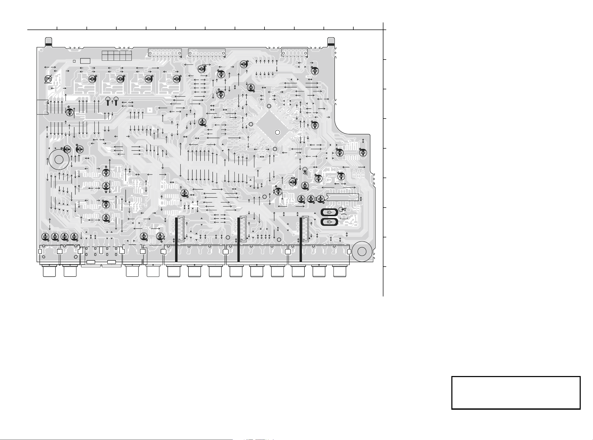
85
鉛フリー半田
半田付けには、鉛フリー半田 (Sn-Ag-Cu) を使用してください。
Lead-free Solder
When soldering, use the Lead-free Solder (Sn-Ag-Cu).
VIDEO (COMPONENT SIDE)
8U-110085
631010085006S
( )
( )
( )
( ) ( )
[VSDA]
[VSCL]
IN
ICTOPADJ
FI
7020-06951-000-0S
VIDEO B'D
MP1
20.0
JV41
JV43
17.5
15.0
JV45
JV46
15.0
JV47
JV48
K1001
K1002
K1003
12.5
JV50
7.5
JV51
JV52
7.5
JV53
12.5
JV54
25.0
JV55
JV56
20.0
JV57
22.5
K1011
12.5
JV59
K1012
K1013
12.5
JV60
12.5
JV61
15.0
JV62
25.0
JV63
JV200
JV64
25.0
JV201
12.5
JV66
JV202
20.0
JV67
JV203
JV68
22.5
7.5
JV204
15.0
JV69
L1001
L1002
JV70
7.5
JV71
12.5
JV72
15.0
JV73
JV75
12.5
JV76
12.5
JV77
JV78
7.5
JV81
15.0
JV82
JV83
20.0
JV85
JV87
JV88
7.5
JV89
25.0
JV90
JV91
15.0
25.0
JV92
JV93
JV94
JV95
17.5
15.0
JV96
17.5
JV97
7.5
JV99
K2001
K2002
K2003
K2011
R2151
R2152
N2001
N2002
N2003
N2004
Q1004
C1013
C1014
C1015
C1016
C1022
C1025
C1026
C1029
C1030
C1032
C1036
JV100
15.0
JV101
JV102
7.5
JV103
15.0
JV104
20.0
JV105
12.5
JV106
JV107
25.0
15.0
JV108
25.0
JV109
JV110
JV112
12.5
15.0
JV113
12.5
JV114
15.0
JV116
JV117
12.5
JV118
20.0
JV119
N3001
N3002 N3003
JV120
7.5
25.0
JV121
12.5
JV122
20.0
JV123
20.0
JV124
7.5
JV125
JV127
22.5
12.5
JV128
C2005
JV129
C2006
C2007
C2008
C2009
JV130
25.0
JV131
17.5
JV132
JV133
C2010
JV134
C2011
17.5
JV135
C2012
JV136
JV137
JV138
17.5
12.5
JV139
C2017
C2018
12.5
JV140
25.0
JV141
22.5
JV142
20.0
JV144
15.0
JV145
JV146
12.5
12.5
JV147
JV148
JV149
22.5
JV150
7.5
JV151
JV152
20.0
12.5
JV153
12.5
JV154
C2031
JV155
C2032C2033
C2034
JV158
U1001
JV1
12.5
JV159
JV2
12.5
7.5
JV3
12.5
JV5
25.0
JV6
JV160
JV161
7.5
JV9
JV162
22.5
JV163
JV165
JV166
JV167
22.5
7.5
JV168
JV169
15.0
C2047
JV170
25.0
15.0
JV171
12.5
JV172
12.5
JV173
JV174
C2051
JV175
22.5
JV176
12.5
JV177
12.5
JV179
JV181
JV182
7.5
JV183
17.5
JV184
C2060
C3001
22.5
JV186
25.0
JV187
12.5
JV188
7.5
JV189
C2065
C2068
C2069
JV190
JV191
JV192
JV193
12.5
JV194
17.5
JV195
17.5
JV196
C2073
C2074
20.0
JV198
JV199
C2077
C2078
JV11
JV12
7.5
JV16
12.5
JV17
12.5
JV19
JV20
12.5
JV21
JV22
15.0
JV23
JV24
20.0
JV25
25.0
25.0
JV26
JV27
7.5
JV28
X1001
25.0
JV29
X1002
JV30
17.5
12.5
JV31
JV32
25.0
JV33
15.0
JV34
25.0
JV35
25.0
JV36
22.5
JV38
15.0
JV39
K2005
K2021
25.0
JV58
JV74
17.5
20.0
JV205
B2001
B2002
B2003
B2004
B2005
JV206
7.5
JV207
JV157
12.5
JV209
JV208
7.5
JV210
JV211
7.5
JV212
17.5
JV213
12.5
JV215
12.5
JV214
JV216
JV217
JV219
JV221
JV224
JV225
JV226
JV227
JV230
JV231
7.5
JV222
7.5
JV223
7.5
JV228
7.5
JV229
JV232
JV233
JV234
JV235
JV13
12.5
JV111
12.5
17.5
JV218
17.5
JV236
17.5
JV237
JV98
JV7
20.0
JV164
22.5
JV143
25.0
JV238
7.5
JV220
JV240
JV84
12.5
25.0
JV239
JV8
17.5
JV42
20.0
15.0
JV241
JV4
12.5
JV243
JV65
JV244
JV245
JV246
17.5
JV247
12.5
JV248
15.0
JV242
7.5
JV249
B2006
JV80
25.0
JV49
20.0
JV86
20.0
JV79
15.0
JV14
JV126
22.5
JV10
22.5
JV37
20.0
JV250
JV251
JV178
15.0
JV180
22.5
20.0
JV252
JV15
22.5
JV44
22.5
JV115
15.0
JV185
25.0
JV253
JV254
JV156
22.5
JV197
25.0
JV18
17.5
JV255
JV256
0
UPUP UPUP UPUP
LOW
LOW
UPUP
C
C
YY
B
E
C
121110987654321
I
H
G
F
E
D
C
B
A
Page 86

86
VIDEO (FOIL SIDE)
U3001
U3002
U1002
U1003
U2001
U2002
U2003
U2005
U2006
U2007
U2008
R2090
R2091
R2092
R2093
R2094
R2096
R2098
R2100
R2101
R2102
R2103
R2104
R2105
R2106
R2107
R2108
R2109
R2110
R2111
R2112
R2113
R2114
R2115
R2116
R2117
R2118
R2119
R2120
R2121
R2122
R2123
R2124
R2125
R2126
R2127
R2128
R2129
R2130
R2131
R2132
R2133
R2134
R2135
R2138
R2139
R2140
R2141
R2142
R2143
R2153
R2154
R2155
C1001
C1002
C1003
C1004
Q1001
C1005
Q1002
C1006
Q1003
C1007
C1008
Q1005
C1009
Q1006
C1010
C1011
C1012
C1017
C1018
C1019
C1020
C1021
C1023
C1024
D1001
D1002
D1003
C1027
D1004
C1028
R1001
R1002
R1003
R1004
R1005
R1006
R1007
R1008
C1031
R1009
C1033
C1034
C1035
C1037
C1038
R1010
R1011
R1012
R1013
R1014
R1015
R1016
R1017
R1018
R1019
R1020
R1021
R1022
R1023
R1024
R1025
R1026
R1027
R1028
R1029
R1030
R1031
R1032
R1033
R1034
R1035
R1036
R1037
R1038
C2001
R1039
C2002
C2003
C2004
Q2001
Q2002 Q2003 Q2004
R1040
R1041
Q2005
R1042
Q2006 Q2007
R1043
Q2008
R1044
R1045
Q2009
R1046
R1047
R1048
C2013
Q2010
C2014
C2015
Q2011
C2016
Q2012
C2019
C2020
C2021
C2022
C2023
C2024
C2025
D2001
C2026
D2002
C2027
D2003 D2004
C2028 C2029
R2001
D2005
R2002
D2006
R2003
D2007 D2008
R2004
D2009
R2005
R1
R2
R2006
R2007
R3
C2030
R2008
R4
R2009
R5
R6
R7
C2035
C2036 C2037
R2010
C2038
R2011
C2039
R2012
R2013
R2014
R2015
R2016
R2017
C2040
R2018
C2041
R2019
C2042
C2043
C2044
C2045
C2046
R2020
C2048
R2021
C2049
R2022
R2023
R2024
R2025
R2026
R2027
R2028
C2050
R2029
C2052
C2053
C2054
C2055
C2056
C2057
R2030
C2058
R2031
C2059
R2032
R2033
R2034
R2035
R2036
R2037
R2038
R2039
C2061
C3002
C2062
C3003
C2063
C2064
Q3001
Q3002
C2066
C2067
R2040
R2041
R2042
R2043
R2044
R2045
R2046
R2047
R2048
C2070
R2049
C2071
C2075
C2076
R2050
C2079
R2051
R2052
R2053 R2054 R2055 R2056
R2057
C2080
R2058
C2081
R2059
R2060
R3001
R2061
R3002
R2062
R2063
R3003
R3004
R2064 R2065 R2066
R2067
R2068
R2069
R2070
U2004
R2071
R2072 R2073 R2074
R2075 R2076 R2077
R2078
R2079
R2080
R2081
R2082
R2083
R2084
R2085
R2086
R2087
R2088
R2089
R1051
R1054
R1055
R1058
R1059
R1052
R1057
R1060
R1053
R1050
R1049
R1056
R9
R8
123456789101112
I
H
G
F
E
D
C
B
A
鉛フリー半田
半田付けには、鉛フリー半田 (Sn-Ag-Cu) を使用してください。
Lead-free Solder
When soldering, use the Lead-free Solder (Sn-Ag-Cu).
Page 87

87
鉛フリー半田
半田付けには、鉛フリー半田 (Sn-Ag-Cu) を使用してください。
Lead-free Solder
When soldering, use the Lead-free Solder (Sn-Ag-Cu).
DIGITAL (COMPONENT SIDE)
s
HRDE
HRVSYNC
HRHSYNC
INPUTHSN
HSCL
HSDA
VOUTHS
VOUTDE
VOUTVS
INPUTHSN
INPUTDE
IPSDA
DDCCLK
DDCDATA
DDCDATA
DDCCLK
DDCDATA
DDCCLK
SRCfs
SRC64fs
SRCDATA
DONE
G
VCC
OUT
G
VCC
OUT
VCC
IN
G
OUTVCC
G
105
104
52
1
208
156
157
109
108
73
72
36
1
144
37
1
TOPTOP
7
1
23
TOP
1
TOP
7
1
7
TOP
39
40
1
2
5
TOP
1
1
10
TOP
A
1
9
R
A
19
R
1
4
TOP
1
4
TOP
1
TOP1TOP
11
1
TOP
11
1
TOP1TOP
7
10
TOP
1
1
18
A
V
TOP
1
8
TOP
1
1
20
A
Y
633010051207S
8U-310051-1
MP3
Z5300
M
H
J
M
H
K
N
E
E
G
F
C
C
D
D
P
F
K
P
G
J
N
A
A
Q
Q
R
R
S
S
( )
( )
T
T
K1001
K1002
K1003
U2800
U2801
U2802
U5300
K2800
K5300
K5301
K5302
N1800
N1801
N4900
N4901
N4902
N4903
N4904
N4906
N4907
N4908
N4910
N4911
N4912
N4913N4914
N4916
K1100
K1101
K1102
C1239
C1839
D5305
N4201
N4600
B9000
N4610
Z1
Z2
Z3
N4200
U3200
N3901
U4202
U4601
U4602
U4603
U4604
U4605
N4905
U1803
N4401
U2001
R3800
S3200
R3224
R5358
R2284
C1118
R5359
R3225
C1119
R2285
R3802
R3226
R2286
R3227
R2287
R3805
R3229
R5552
R3806
C9012
C3253
R3807
R5553
C9013
C3254
R5554
C9015
R5555
R5361
U5102
C3832
R5362
C9016
C3833
C9017
R5363
U5104
C9018
C3834
R5364
D1100
U5105
D1101
R3231
R5365
C1125
U5106
D1102
C3836
R3232
R5366
R3233
U5107
C3837
D1103
C1127
R3810
R3234
D1104
U5108
D1105
R3811
C3839
R3235
R5369
R1101
R3236
R3812
D1106
R1102
R3813
D1107
R3237
R1103
D1108
C9020
C3260
R3238
R3814
R1104
R3815
C4201
C9021
R3239
D1109
U5301
R1105
R3816
R3817
R3818
C9024
R5370
Q4200
R3819
C3265
C3841
C9025
C3842
C3266
R5372
Q4202
C3843
C9027
C4207
C3844
R3240
D1110
R5374
C4208
C9028
C3845
R3241
D1111
D1112
C3846
R3242
D1113
R5377
U5500
R3820
R5378
R1110
R3244
D1114
R3821
D1115
R1111
C3849
C4401
R5379
R3245
R3822
U5502
D1116
R1112
R3246
R3247
R3823
R1113
D1117
C4404
R3248
D1118
R3824
R1114
C4210
D1119
R3825
R3249
C4405
C4211
R1115
C9031
R3826
R1116
C4212
R1117
R3827
Q4403
R1118
C3850
R5380
C3851
R5381
C4215
R1119
C3852
C4216
R5382
C3853
R5383
C4600
R5384
D1120
D1121
R5385
C4601
D1122
C4602
R3252
R5386
C4603
R5387
D1123
R1120
D1124
C3858
R5388
C4604
C1148
D1125
C3859
R1121
R5389
R1122
D1126
D1127
R1123
D1128
D1129
C9042
R3836
C4222
R1126
R3837
R1127
R3838
C3860
D4200
R5390
C4224
R3839
C3861
R5391
D4201
R1129
C4225
C1151
D4202
C1152
D4203
C4610
C9048
D1130
C1154
U3000
R3261
D1131
C1155
R3262
C3866
R5396
D1132
R3263
C3867
R5397
R1130
R3264
C3868
C4420
R4204
R1131
R3265
C3869
C4422
R1132
R1133
R3844
C4618
R3268
C4230
R1134
R3845
R3269
C4231
R3846
R3847
R3848
R4400
C9054
R3849
R4401
C9055
C1162
C9057
C1163
C9058
R3270
C3874
R3271
C3875
C4622
R3272
R4406
R3273
R4407
C4623
C3878
R3274
C4624
R3275
C4625
R4215
R4409
C4626
R4216
R4217
C4627
C4628
R4600
R3854
R4218
Q4624
C9061
R3855
C4435
C4629
R4601
Q4625
R3856
C9062
R4602
C4242
Q4626
R4603
R3857
C4243
Q4627
C9064
Q4628
R3858
C4244
R4604
R1148
R3859
R4605
C4245
C4439
Q4629
R1149
C4246
R4412
C4247
R4413
C9068
C4630
R4414
C4248
C4631
R4415
C1175
C4249
R4416
C1176
C4632
C4633
R4223
Q4630
R3860
R4224
R1150
C4634
C4635
R3861
R4419
C4441
R1151
C4636
R4226
C4442
R1152
R4227
R1153
C4637
C4638
R1154
C4250
Q4635
R1155
C4639
C4251
C9072
C4446
R1156
C9073
R1157
C9074
R4420
R1158
R4421
C1181
R1159
R4616
C9076
R4422
R4617
C9077
R4423
C4640
U3800
C9078
R4619
C4641
R4425
U3802
R4426
C4642
R4427
R3870
U3804
R4428
N3900
R4234
R1160
U3805
R3871
R4429
R3872
R1162
R3873
C4453
R3874
C4648
C9080
C4454
R4238
R1164
R4621
C4455
R3875
C4649
C9081
R4239
N1001
R1165
R3876
R4622
C9083
R3877
R1167
R4623
R1168
R4624
Q4648
R4625 R4626
C9087
R4627
R4433
C4650
R4628
R4240
U1100
C4651
R4241
R4435
R4629
R4436
C4652
R4242
C4653
R4243
C4654
X5301
C4655
R1172
C4463
C9090
C2524
R4630
R4631
C4465
C2525
R3886
R4632
C2526
C4466
R4633
R3887
C9093
R1177
C4467
R3888
L4900
C9094
R4634
C4468
R3889
L4901
C9095
R4635
C4469
L4902
L4903
R2503
L4904
R4444
R2504
X5501
L4905
R4445
R4639
R2505
L4906
C4662
L4907
L4908
R1180
R4448
C4470
L4909
R4449
C4667
R4640
R4641
R4642
R4643
C2537
L4910
R4644
N1600
L2200
L4911
N1601
R4645
L2201
L4912
R4646
R2512
L4913
L4914
L4915
C4671
L4916
C4672
C4673
L4917
L4918
C4674
C4675
L4919
R4651
C4679
R5400
U4200
L4920
L4921
U4201
L4922
L4923
U4203
L4924
C4680
L4925
C4681
L4926
C4682
L4927
C4683
L4928
C4684
L4929
U4400
C4689
X3201
U4403
U4404
L4930
L4931
L4932
L4933
L4934
L4935
C4691
L4936
L4937
L4938
U4600
C4694
L4939
C4699
U4606
U4607
L4940
L4941
L4942
L4943
L4944
L4945
L4946
L4947
L4948
L4949
L4950
C3900
N4909
L4951
C3901
L4952
C3902
L4953
L4954
C3904
Q3900
C8531
L4955
Q3901
C1001
C8532
L4956
C1002
L4957
C8533
C3907
C8534
L4958
N2200
C8535
L4959
Q1001
N2201
C8536
Q1002
C1006
C8537
Q1003
C8538
C1008
Q1004
C8539
Q1005
L4960
L4961
C1201
L4962
X1102
L4963
X1103
L4964
C8540
L4965
C8541
C1205
C8542
L4966
C1012
L4967
C8544
L4968
C1208
L4969
C8545
C8546
C1016
C8547
C1017
U2500
U2501
L4970
L4971
C1212
C8551
C8553
L4977
L4978
R3900
N5100
C8555
L4979
C3929
R3901
D1001
C8556
R3902
C8557
R3903
C8558
R3904
C1604
C8559
R1001
C1605
C1606
R1002
R1003
C1607
L4980
R1004
C1608
C1220
L4981
C1609
R1005
L4982
R1006
L4983
L4984
N5300
L4985
N5301
C1225
C1801
L4986
L4987
C1803
L4988
R3910
C1610
C1804
C1228
L4989
R3911
C1805
C1611
R3912
C1612
C1806
Q1803
R3913
C1807
C1613
R3914
C1808
C1614
R3916
R3917
L4990
N5500
R3918
C1232
R1017
R1018
L4995
R1019
L4996
C1236
L4997
L4998
R3920
L4999
X4401
C1815
R3923
R3924
R1020
R1021
C1819
R3926
C3950
R1600
R3929
C3951
C3952
C3953
C3954
C1820
L1100
C3955
C4701
R1605
C3956
C4702
L1102
C3957
R1607
C4703
R3930
C3958
D1800
C1824
C3959
R1609
C1825
D1801
R3932
C4706
C1632
D1802
R3933
C4707
D1803
C1827
N3000
C4708
C1634
D1804
D1805
C1829
C4709
D1806
R1803
D1807
C4900
R1804
D1808
R1610
C4901
R1611
D1809
R1805
C4902
R1612
C4903
R1613
C4904
R1614
C1830
C4905
R1615
C4906
R1616
C4712
C1832
C4907
C1833
R1617
N3200
C4908
C1834
D1810
R1618
C4715
D1811
R1619
C2005
C1835
Q2001
C4716
D1812
C1836
C2006
C4717
C1837
D1813
C2007
C4718
C1838
R1810
D1814
R3945
D1815
C4719
R1811
R3946
D1816
R3947
R1813
D1817
C4910
R3948
R1814
D1818
R1620
R3949
C2201
D1819
R1621
C4912
R1622
C2202
C4913
R1623
C2203
C4720
S1600
R1625
C2011
C4916
C4722
C2012
R1626
C4917
C2013
C4723
R1627
C4918
R3950
C4724
D1820
R1628
C4919
R3951
D1821
C1651
R1629
C2015
R3952
C4726
D1822
C2016
C4727
R3953
C2017
C4728
C1654
C2018
C4729
C1656
C1657
C4920
L4200
R1824
C1658
R1630
C4921
L4201
R1631
C1659
C4922
R1632
R1826
C4923
R1633
C2213
R1827
L4204
C4730
R1828
C2020
R1634
C4925
R1829
R1635
C4731
C2215
R1636
C4732
L4207
C4733
C4927
R1637
C2217
R4900
R1638
R4901
C4735
C2219
R1639
L4209
R4902
C4736
R4903
C4738
L4400
R1830
L4401
R1831
C1665
L4402
C1666
R2002
R1832
R2003
C1667
R1833
L4403
C5100
R1640
R1834
L4404
L4210
C5101
C2221
R1641
R1835
C1669
L4405
L4211
L4212
L4406
C5102
R1642
R1836
R2006
C5103
R1643
R2007
C2223
R1837
C5104
U3900
C2800
Q5100
R2008
R1838
C2801
Q5101
R2009
C2225
C4741
R1839
Q5102
C2802
U3902
C5107
C4743
C2803
C2227
C5108
L4600
C2804
C2228
C4744
L4601
C2805
R2201
C2229
Q5106
C2806
L4602
U1002
C4746
Q5107
C2807
L4603
L4604
C4748
Q5108
C5300
C2808
R1840
Q5109
L4605
C5301
R2011
C4749
R1841
L4606
C5302
R1842
R2012
L4607
C5303
R1843
R2013
C5110
C5304
L4608
R2014
C2230
R1844
C5111
C5305
L4609
R2015
R1845
C5112
C5306
R2016
C5307
R1653
R2017
C5308
C4750
R1654
R2018
C5309
R1655
C4751
C5116
Q5306
R1656
Q5307
R1657
L4610
C5500
Q5308
C4754
R1658
L4611
C5501
Q5309
R1659
L4612
C5502
C2816
C5503
C2817
C5310
C4758
C2818
L4615
C2819
C4759
L4616
C5312
L4617
C5314
R1854
L4618
R1660
L4619
R1855
C8002
C2242
R1662
C5317
C8003
C2243
C2244
C4760
R1664
Q5315
C2821
C8007
C4763
C2823
L4620
D2800
R5100
C8008
R1668
C4764
L4621
R5101
D2801
C8009
C4765
R1669
L4622
C5512
L4623
C4767
C2827
R5104
R2800
L4624
R1860
C5321
R5105
R2801
U1601
R1861
R5106
C5322
R2802
U1602
R1862
R2226
R5107
R2803
U1603
R2227
L4628
D5300
R5108
C8010
R2228
U1604
R1864
R1670
D5301
C8011
R1865
U1605
R2229
R1671
D5302
R1866
R1672
U1606
C8013
D5303
R1673
U1607
R1867
R5300
D5304
C8014
R1868
C2254
R1674
R1869
R5301
C2255
R5302
D5306
C2256
R1676
D5307
C3003
C2257
C2833
R1677
R5110
D5308
C2834
R2230
R1678
C2258
R5111
D5309
C2259
U1801
R1679
C3005
C2835
R5112
R5113
C2837
R1870
R5114
R2810
U1804
R5115
R2811
C2839
R2812
R2813
C3200
R5500
R5118
D5310
R1680
C3201
R5501
D5311
R1681
R5502
R1682
R5503
R1683
L5000
R5310
N4400
R1684
C4780
L5001
C4781
R5506
L5002
C2266
C3207
L5003
R5507
R5313
L5004
R5314
R5508
C3014
C2844
L5005
R5315
C2845
L5006
R5316
C4786
C2846
R5123
C4787
R5317
L5007
R2243
C2847
R5318
L5008
C2848
R2244
L5009
R2245
C2849
R5510
C3211
R5511
R5512
R5514
L5010
C4791
R5515
L5011
R5321
R5322
L5012
C2276
R5517
L5013
L5014
R5518
R5324
C3218
L5015
R5325
R2251
L5016
R5326
L5017
R5327
L5018
R3000
R5135
C4799
L5019
R3001
R5136
R3002
R3003
R2257
R5137
R5520
C3220
R2258
R3004
R5138
R5521
C3221
R3005
R5522
R3006
C3223
L5020
C3800
L5021
R5525
R3009
C3802
R5526
L5022
R5332
C3226
L5023
C3227
L5024
C3804
R5334
R2260
L5025
R3201
C3805
R5335
R2261
C3806
R5336
R2262
U2002
C3807
R3203
R5337
R2263
R5338
L5028
R3205
R5339
L5029
R3011
R3206
R2266
R2842
R3012
R3013
R2843
R2267
R5530
X3900
R2268
R2269
R3209
L5030
C3810
R5340
C1100
U2200
C3811
L5031
R5341
C1101
L5032
C1102
L5033
R5343
C1103
C3814
R3210
L5034
Q1100
C1104
Q1101
C3815
L5035
R5345
C1105
L5036
R3212
Q1102
C1106
R3213
L5037
R5347
Q1103
C1107
C3818
L5038
Q1104
R3214
C1108
Q1105
R3215
R5349
C1109
R3021
R2275
R3216
R2276
R3217
R3218
C3240
C9001
R3219
R3026
C9003
R5350
C1110
C9004
C3245
C1111
C3246
C9006
C1112
C3823
R5353
C9007
C3824
R3220
C1114
C9009
R3221
C3825
C1115
R2281
R5356
C1116
R2282
R3223
C3827
R2283
2
1716151413121110987654321
H
G
F
E
D
C
B
A
FRONT HDMI (COMPONENT SIDE)
TOP
1
R20
C21
C22
R17
R16
L4
8U-310051-2
FRONT HDMI
R18
U2
C16
R14
L2
Q2
Q1
C1
R5
R3
R1
R13
R4
R2
R19
C18
C17
R15
N1
C20
C19
R8
C4
R12
C7
R10
21
1
MP2
A
23
R11
C9
C5
L3
C6
C8
R9
U1
C3
C2
L1
B
K1
C
Page 88

88
鉛フリー半田
半田付けには、鉛フリー半田 (Sn-Ag-Cu) を使用してください。
Lead-free Solder
When soldering, use the Lead-free Solder (Sn-Ag-Cu).
1234567891011121314151617
H
G
F
E
D
C
B
A
L
R
L
R
B
B
C
C
A
C
A
C
C3828
C3829
R3801
R3803
C3250
R3228
R3804
R5550
C9010
R5551
C3251
C9011
C3252
R3808
C9014
C3830
R5360
U5100
C1120
C3831
R3809
C3255
U5101
C1121
C3256
R5556
C1122
C3257
U5103
R5557
C1123
R3230
C3258
R5558
C1124
C3835
C3259
R5559
C9019
C1126
U2803
R5367
C3838
R5368
U2804
C1128
R1100
U5109
U2805
C1129
U2806
U2807
R5560
C4200
R5561
C3261
R5562
C3262
C4202
U5302
R1106
C9022
C3263
C4203
R1107
C9023
R5563
C3264
C3840
C4204
R1108
C1130
R5564
R5371
Q4201
C4205
C1131
R1109
C4206
C1132
C9026
C3267
R5373
Q4203
C1133
C3268
C1134
C9029
R5375
C4209
C3269
C1135
R5376
C1136
C3847
R3243
C1137
C3848
C4400
C1138
U5501
C1139
C4402
C4403
C9030
C3270
Q4400
C3271
Q4401
C9032
C3272
C4406
Q4402
C9033
C3273
C4407
C4213
C4408
R3828
C3274
L3900
Q4404
C4214
C1140
R3829
C9035
C3275
Q4405
C4409
L3901
C1141
C9036
C3276
L3902
C1142
C3277
C4217
C9037
C1143
C9038
R3250
C3854
C3278
C4218
C1144
C3855
C3279
R3251
C4219
C1145
C9039
C3856
C1146
R3253
C3857
C1147
R3830
R3254
Q4600
C4410
R3255
R3831
C4411
Q4601
C1149
Q4602
R3832
R3256
C4412
R3833
Q4603
R3257
C4413
R3258
R3834
C3280
C4414
C4220
R1124
C9040
R3835
R3259
C4415
C4221
C9041
R1125
C4416
C4417
C4223
C9043
C9044
C4418
C4800
C1150
R1128
C4801
C4419
C9045
C9046
C3862
R5392
C4802
C4226
C3863
C4803
R5393
C4227
C1153
C9047
C3864
R3260
R5394
R4200
C4228
C3865
C4611
R5395
C4229
R4201
C9049
U3001
R4202
C1156
C4612
C4613
R4203
D1133
C1157
C4614
R3840
R5398
C1158
R3841
R5399
C4421
R4205
C1159
C4615
Q4612
R3842
C4616
R3266
R4206
Q4613
R3843
R3267
C4423
R4207
C4617
Q4614
C9050
C4424
R4208
C4619
C4425
R4209
C9051
Q4615
R1135
C4426
C4232
C9052
R1136
Q4616
C9053
C4427
C4233
R1137
Q4617
C3870
C4428
C4234
R1138
Q4618
C1160
U3201
Q4619
C3871
C4429
C4235
C1161
R1139
C3872
C9056
R4402
C4236
U3202
C3873
R4403
C4237
C4620
R4404
C4238
R4210
C1164
C9059
R4211
R4405
C4239
C1165
C4621
R4212
C1166
C3876
R4213
C1167
C3877
R3850
R4408
R4214
D4600
C4430
Q4620
R1140
C1168
L1600
Q4621
R3851
C4431
D4601
L1601
C1169
R1141
R3852
Q4622
R3276
C4432
R1142
Q4623
R3277
R3853
C4433
R1143
R3278
C4240
C4434
R1144
C9060
R3279
R4219
C4241
R1145
X2201
C4436
R1146
C4437
R1147
C9063
R4410
C4438
C1170
R4411
C9065
C1171
C9066
R4606
C1172
C1173
C9067
R4607
R4608
R4220
C1174
L1800
R4609
R4221
C9069
L1801
R4222
L1802
R4417
C1177
L1804
C4440
R4418
C1178
C2500
Q4631
R4225
C1179
C2501
R3862
Q4632
C2502
Q4633
R3863
C4443
C2503
R3864
C9070
Q4634
R4228
C4444
C2504
R4610
R4611
R3865
C4445
R4229
C2505
C9071
R3866
Q4636
C2506
R4612
R3867
Q4637
R4613
C4447
C2507
R4614
R3868
C4448
Q4638
C1180
C2508
R3869
C4449
Q4639
R4615
C2509
C9075
C1182
C1183
R4618
R4424
R4230
C1184
U3801
R4231
C9079
C1185
R4232
C1186
U3803
C4643
R4233
C1187
Q4640
C4450
C2510
C4644
C1188
C4645
Q4641
R4235
C4451
R1161
C1189
C2511
U3806
C4646
C4452
Q4642
R4236
C2512
U3807
R4237
R1163
C4647
C2513
Q4643
R4620
C2514
Q4644
C2515
Q4645
U3809
C4456
C2516
Q4646
C9082
R1166
C4457
C2517
Q4647
C9084
C4458
R4430
R3878
C1190
C2518
R4431
C4459
R3879
C9085
X2801
C2519
R1169
C1191
C9086
R4432
C1192
C1193
R4434
C9088
C1194
C9089
C1195
U1101
C1196
R4437
C1197
R3880
C4460
R4438
C2520
R1170
C1198
R3881
C4461
R4439
C2521
R1171
C1199
R3882
C4656
C4462
C2522
C4657
R3883
R1173
C2523
R3884
C4464
R1174
C4658
C4659
C9091
R3885
R1175
C9092
R1176
C2527
R4440
R1178
R2500
C2528
R4441
C2529
R2501
R1179
R4636
R4442
R2502
R4637
R4443
C4660
R4638
L2000
C4661
R4446
R2506
R4447
C4663
R2507
R3890
C4664
R2508
C2530
R3891
C4665
C2531
R2509
R3892
C4666
C2532
R3893
C2533
C4668
C2534
R3894
C4669
C2535
R3895
C2536
R3896
R3897
R2510
C2538
R3898
R2511
C2539
R3899
L2202
R4647
L2203
R2513
R4648
C4670
R2514
L2204
R4649
L2205
R2515
C2540
C2541
C4676
C2542
C4677
C2543
C4678
R4650
C2544
C2545
R4652
C2546
R4653
C2547
R4654
R5401
R4655
R5402
R4656
R4657
R4658
U4204
R4659
U4205
C4685
C4686
C4687
R4660
C4688
R4661
U4401
R4662
U4402
R4663
R4664
R4665
U4405
R4666
R4667
C4690
R4668
R4669
C4692
C4693
C4695
C4696
C4697
R4670
C4698
R4671
R4672
R4673
U4608
R4674
C3903
C8530
C3905
C3906
C1003
C3908
C1004
C3909
C1005
C1007
C1009
Q1006
Q1007
C3910
Q1008
C1200
C3911
Q1009
C3912
C1202
C3913
C1203
C3914
C1010
L3000
C1204
C3915
C1011
C3916
C1206
C8543
C3917
C1013
C1207
C3918
C1014
C3919
C1209
C1015
C8548
C1018
C8549
C1019
C3920
C1210
C3921
C1211
L4972
C3922
L4973
C3923
C1213
L4974
C8550
C3924
C1214
L4975
C3925
C1215
L4976
C8552
C3926
C1216
C3927
C1217
C8554
C3928
C1600
C1218
C1219
C1601
C1602
C1603
Q1600
R3905
Q1601
R3906
R3907
C3930
R3908
C3931
R3909
C1221
C3932
C1222
C3933
R1007
C1223
C3934
R1008
C1224
C1800
C3935
R1009
C3936
C1226
C1802
C3937
C1227
C3938
Q1800
C3939
C1229
Q1801
Q1802
R1010
R3915
R1011
C1615
C1809
C1616
R1012
R1013
C1617
C3940
C1618
R1014
C1230
L4991
R3919
C3941
C1231
C1619
R1015
L4992
C3942
R1016
L4993
C3943
C1233
L4994
C3944
C1810
C1234
C3945
C1811
C1235
L3801
C3946
C1812
C3947
C1237
C1813
C3948
C1814
C1238
C1620
R3921
C3949
C1621
R3922
C1816
C1622
C1817
C1623
C1624
C1818
R3925
C1625
C1626
R1022
R3927
R1023
C1627
R3928
R1024
C1628
R1601
C1629
R1025
R1602
R1026
R1027
R1603
R1604
C4700
C1821
L1101
R1606
C1822
C1823
C4704
R1608
C1630
C4705
R3931
C1631
C1826
C1633
R3934
R1800
C1828
R3935
C1635
R1801
R3936
C1636
R1802
R3937
C1637
R3938
C1638
R3939
C1639
R1806
R1807
C2000
R1808
C4710
C4711
R1809
C1831
C2001
C2002
C4713
C2003
R3940
Q2000
C2004
C4714
C1640
C4909
R3941
C1641
R3942
C1642
R3943
C1643
R3944
C2008
C1644
C2009
C1645
C1646
R1812
C1647
C2200
C1648
C4911
R1815
C1649
R1816
R1817
C4914
R1624
Q2200
R1818
C2204
C2010
C4915
C4721
C2205
Q2201
R1819
C2206
C2207
C2208
C1650
C2014
C4725
C2209
C1652
C1653
R1820
R1821
C1655
C2019
R1822
R1823
C2210
C2211
R1825
L4202
C2212
L4203
C4924
C2214
L4205
C4926
L4206
C2216
C4928
L4208
C2218
C4734
C1660
C4929
C1661
C1662
C1663
C4737
C1664
R2000
R2001
C4739
C1668
R2004
C2220
R2005
C2222
R1644
C2224
C4740
C5105
U3901
R1645
C5106
R1646
C2226
C4742
Q5103
R1647
Q5104
C1670
R1648
R2200
C5109
Q5105
R1649
C4745
U1001
C1671
R2202
R2203
C4747
R2204
R2010
R2205
C2809
R2206
R2207
Q5300
R1650
R2208
Q5301
C2231
R1651
R2209
Q5302
C2232
R1846
R1652
C5113
Q5303
R1847
C2233
Q5110
C5114
C2810
Q5304
R1848
C2234
Q5305
C5115
C2811
Q5111
C2235
R1849
C2812
C4752
C2236
Q5112
C5117
C4753
C2237
C2813
Q5113
C5118
C2814
C2238
R2210
Q5114
C5119
C2815
C2239
C4755
R2211
Q5115
C4756
R2212
C4757
L4613
R2213
L4614
Q5500
C5504
R1850
R2214
C5505
Q5501
C5311
R2215
R1851
Q5502
C5506
R2216
R1852
Q5503
C5507
C5313
R1853
R2217
Q5504
C5120
Q5310
C5508
R2218
C2240
C5509
Q5505
Q5311
C5315
R1661
C2241
R2219
C5316
Q5312
R1856
Q5506
Q5313
R1663
R1857
C5318
Q5314
R1858
C2820
C5319
R1665
C4761
R1859
C2245
C4762
R1666
C2822
C2246
R1667
C2247
C5510
C2248
R2220
C2824
C5511
C2249
R2221
C2825
R5102
C4766
R2222
C2826
C5513
R5103
R2223
C5514
C4768
C5320
U1600
C2828
C5515
L4625
C2829
R2225
C4769
C5516
L4626
C5517
L4627
C5323
R1863
C5324
R2804
C2250
R5109
C5325
R2805
C2251
C5326
R2806
C8012
C2252
C5327
R2807
C2253
C4770
R2808
C3000
C2830
R2809
R1675
C2831
C4771
C3001
C4772
C2832
C3002
C4773
R5303
C4774
R5304
C3004
U1800
R5305
C4775
R2231
C4776
C2836
C3006
R2232
U1802
C4777
R2233
C3007
R5308
D5500
L2500
C2838
R2234
C3008
C4778
C4779
R5309
C3009
L2501
R2235
R5116
R2236
R5117
R2237
R2238
R2814
C2260
R5119
R2815
R2239
C2261
R2816
C3202
C2262
R2817
C3203
C2263
R2818
C3204
Q3200
R5504
C2264
C2840
C3010
R5311
R5505
R2819
Q3201
C3205
C2265
C2841
C3011
R5312
C3206
C4782
C3012
C2842
C2843
C3013
C4783
C2267
C4784
C3208
R5120
R2240
C2268
R5121
C3209
R5509
C4785
C2269
R2241
R5122
R2242
R2820
R5124
C4788
R2821
R5125
R5319
C4789
R5126
R2822
R2246
R2823
R5127
R2247
R2824
R5128
C3210
C2270
R2248
R5129
R2825
C2271
R2249
C3212
R2826
C2272
C3213
R5513
C2273
R2827
C4790
C3214
R5320
R2828
C2274
C3215
R2829
C2275
R5516
C3216
C4792
R5323
C3217
C4793
C2277
R5130
C4794
C2278
R2250
R5131
R5519
C3219
C4795
C2279
R5132
C4796
R2252
R5133
C4797
R2253
R5134
C4798
R5328
R2830
R2254
R5329
R2255
R2831
R2256
R2832
R2833
R2834
C2280
R2835
C2281
R2259
R5139
C3222
R2836
C2282
R5523
R2837
R3007
C2283
R5524
C3224
R5330
C2284
R3008
R2838
C3801
C3225
R5331
R2839
C2285
C2286
C3803
R5527
R5333
C2287
R3200
R5528
C3228
U2000
C2288
R5140
R5529
C3229
C2289
R3202
L5026
L5027
R3204
C3808
R2264
R2840
R3010
C3809
R2841
R2265
R3207
C3230
C2290
R3014
R3208
R2844
R5531
C3231
R3015
R2845
C3232
R3016
R5532
R2846
C3233
R3017
R5533
R2847
R5534
C3234
R2848
R3018
R5535
C3235
U2201
R2849
R3019
C3812
C3236
R5536
R5342
R5537
C3237
C3813
R5538
C3238
R5344
R2270
R3211
R5539
C3239
R2271
C3816
R5346
R2272
C3817
R2273
R5348
R2850
R2274
R3020
L5039
C3819
R2851
Q1106
R3022
R2852
R2853
R2277
R3023
R5540
C9000
R3024
R2854
R2278
C3241
R5541
R2855
R2279
R3025
R5542
C9002
C3242
R2856
R5543
C3243
R2857
C3820
L5040
R5544
C3244
R5351
C3821
C9005
R5545
C3822
R5546
R5352
R5547
C3247
C1113
R5548
C9008
C3248
R5354
R2280
C3249
R5549
R5355
C3826
R3222
R5357
C1117
DIGITAL (FOIL SIDE)
s
FRONT HDMI (FOIL SIDE)
D2
R7
C14
R6
C10
C13
C15
C11
D1
C12
12
C
B
A
Page 89

89
鉛フリー半田
半田付けには、鉛フリー半田 (Sn-Ag-Cu) を使用してください。
Lead-free Solder
When soldering, use the Lead-free Solder (Sn-Ag-Cu).
1110987654321
K
J
I
H
G
F
E
D
C
B
A
INPUT (COMPONENT SIDE)
Page 90

90
鉛フリー半田
半田付けには、鉛フリー半田 (Sn-Ag-Cu) を使用してください。
Lead-free Solder
When soldering, use the Lead-free Solder (Sn-Ag-Cu).
INPUT (FOIL SIDE)
1234567891011
K
J
I
H
G
F
E
D
C
B
A
Page 91

91
鉛フリー半田
半田付けには、鉛フリー半田 (Sn-Ag-Cu) を使用してください。
Lead-free Solder
When soldering, use the Lead-free Solder (Sn-Ag-Cu).
PREOUT (COMPONENT SIDE)
1110987654321
K
J
I
H
G
F
E
D
C
B
A
Page 92

92
鉛フリー半田
半田付けには、鉛フリー半田 (Sn-Ag-Cu) を使用してください。
Lead-free Solder
When soldering, use the Lead-free Solder (Sn-Ag-Cu).
PREOUT (FOIL SIDE)
1234567891011
K
J
I
H
G
F
E
D
C
B
A
Page 93

93
ANALOG AUDIO SIGNAL LINE
AGND
AGND
AGND
AGND
AGND
AGND
R527
150
OPEND445
10K
R504
180K
10K
R466
R460
180K
10K
R423
R417
180K
-B
HIGHGND
SL
DC_DET4
TR_THERMAL
ASO
RADI_THERMAL
AGND
AGND
AGND
AGND
R484
150
OPEND447 OPEND443
C514 330/6.3
C516 OPEN
2.2KR731
R409
150K
R528
1K(1)
R529
1K(1)
1.2K
R705
R461
15K(2)
R420
220K
R445
OPEN
C430
OPEN
C417
OPEN
C416
10/100
C403
10N-K
SR
SL
FR
TR_THERMAL
ASO_DET
DC_DET4
SBL_IN
SBR_IN
FR_IN
SL_IN
SR_IN
C_IN
R523
470K
R514
1.2K
R436
470K
R427
1.2K
33K
R524
R515
0
R496
150K
R452
150K
ZD404
MTZJ5.1A
33K
R437
R428
0
ZD401
MTZJ5.1A
2N2-C
C445
Q431
KTA1268
R485
1K(1)
220P-J
C421
100K
R446
R441
1K(1)
2N2-C
C413
R440
150
Q407
KTA1268
220P-J
C405
100K
R402
R719
220
R486
1K(1)
OPEND446
1.2K
R704
R442
1K(1)
R717
220
1.2K
R703
1SS133T
D418
1SS133T
D412
1SS133T
D406
KTC3206
Q435
D413
1SS133T
R447
270(1)
KTC3206
Q411
R418
15K(2)
R403
270(1)
D401
1SS133T
C443
470P-500V
R487
270(1)
C427
470P-500V
R443
270(1)
C467
OPEN
R507
220K
R520
220K
C499
OPEN
R477
220K
R463
220K
R433
220K
J468
OPEN
J537
C439 47/50
Q433
KTC3964
R509
470
R495
OPEN
OPENJ544
R465
470
R451
OPEN
J416
Q409
KTC3964
R422
470
R404
OPEN
R526
22(1)
C446
OPEN
C433
OPEN
R502
22(1)
R458
22(1)
C414
OPEN
R439
22(1)
R415
22(1)
C402
OPEN
R511
0R47(2)
0R47(2)
R517
0R47(2)
R474
2SD2560
Q416
Q410
2SB1647
R424
0R47(2)
132
TP403
C432
10/100
R456
10K 10K
R457
R413
10K 10K
R414
132
TP401
5.6K
R513
R498
150K
R454
150K
5.6K
R426
+HIGHB
R493
OPEN
R421
22K
Q405
2N5401S
+HIGHB
-HIGHB
HIGHGND
-HIGHB
SR
R508
OPEN
R470
OPEN
C
FL
RADI_THERMAL
DC_DET3
D458
1N4148
R733
150K
SBL_IN
SBR_IN
SL_IN
SR_IN
FL_IN
R480
470K
R471
1.2K
ZD407
MTZJ5.1A
R472
0
33K
R481
100K
R490
220P-J
C437
2N2-C
C429
Q419
KTA1268
OPEND448
R718
220
OPEND444
R505
15K(2)
R491
270(1)
KTC3206
Q423
D407
1SS133T
R530
270(1)
C411
470P-500V
C435
OPEN
J520
R489
OPEN
C423 47/50
KTC3964
Q421
OPEN
J518
C407
R408
OPEN
R483
22(1)
Q434
2SB1647
2SD2560
Q428
R467
0R47(2)
Q422
2SB1647
0R47(2)
R430
2SD2560
Q404
C448
10/100
R500
10K 10K
R501
132
TP402
5.6K
R469
R411
150K
R551
OPEN
12354
CP402
R536 1.2K
C513 330/6.3
C515 47/16
C517 OPEN
2.2KR732
0
R410
C442
100/50
R405
270(1)
R476
2.7K
10/100
C415
C404 OPEN
R506 22K
R499 15K
22KR459
C418
100N-K
22KR416
R406
PRF18BB471QB5RB
OPEN
C419
R712
150
C444
470P-500V
KTA1268
Q43222/50
C440
Q425
KTA1024Y
0
R497
0
R453
R444
1.2K
AGND
R710
150
470P-500V
C412
KTA1268
Q40822/50
C408
1.2K
R401
Q401
KTA1024Y
1SS133T
D417
Q436
KTC3206
R525
220
33K
R516 C441
220P-500V
R492
270(1)
Q426
KTA1024Y
1SS133T
D411
33K
R473 C425
220P-500V
C426
100/50
R478
3.3K(1)
Q414
KTA1024Y
220P-500V
C422
R448
270(1)
1SS133T
D405
R438
220
Q412
KTC3206
R434
3.3K(1)
220P-500V
C406
33K
R429 C409
220P-500V
D415
1SS133T
0R47(2)
R512
0R47(2)
R518
VR403
1K
ZD409
MTZJ4.7B
OPENC436
C431
10/100
0R47(2)
R475
D410
1SS133T
ZD406
MTZJ4.7B
R479
560
ZD405
MTZJ4.7B
D404
1SS133T
R435
560
D403
1SS133T
0R47(2)
R425
VR401
1K
R432
2.7K
ZD402
MTZJ4.7B
2N5551S
Q430
R726
56K
22KR503
Q427
2N5401S
C434
100N-K
R494
PRF18BB471QB5RB
Q415
2N5401S
R462 22K
D408
1SS133T
R455 15K
2N5551S
Q406
R419 22K
D402
1SS133T
56K
R724
R412 15K
C401
100N-K
Q417
OPEN
R407
10K
1N4148
D457
150K
R734
43 126578910111213
CP401
R488
1.2K
KTA1268
Q42022/50
C424
Q413
KTA1024Y
R711
150
C428
470P-500V
220P-500V
C438
R521
3.3K(1)
Q424
KTC3206
R482
220
C410
100/50
Q402
KTA1024Y
10/100
C447
D416
1SS133T
R519
2.7K
ZD408
MTZJ4.7B
R522
560
D409
1SS133T
0R47(2)
R468
VR402
1K
C420 OPEN
0R47(2)
R431
ZD403
MTZJ4.7B
D414
1SS133T
R725
56K
R450
PRF18BB471QB5RB
2N5551S
Q418
Q403
2N5401S
5678910 4 3 2 1
CP403
12354
CN404
PRF18BD471Q
R464
PRF18BD471Q
R449
SBR
SBL
FR
SR
C
SL
FL
AGND
AGNDAGND
AGND
AGND
AGND
AGND
SR
SL
FR
C
FL
C
FL
FR
TR_THERMAL
ASO_DET
DC_DET4
HIGHGND
HIGHGND
-HIGHB
+HIGHB
+HIGHB
RADI_THERMAL
DC_DET3
PREGND
HIGHGND
-HIGHB
+HIGHB
-HIGHB
PAGE 3(A3)
SPK B'D
PAGE 9(04)
AUDIO B'D
PAGE 24(E5)
HDMI B'D
PAGE 3(A5)
SPK B'D
PAGE 2
AMP B'D 2/2_A1
PAGE 2
AMP B'D 2/2_M1
7CH-AMP B'D (1/2)
SCHEMATIC DIAGRAMS (1/37)
10
9
8
6
7
EDCBA HGF
2
3
4
5
FGH
1
ABCDE
4
5
2
3
MNOIJKL
1
LKI
J
MNO
7
6
8
9
10
z
z
z
z
z
s
Page 94

94
C471
47/50
C455 47/50
+HIGHB
-HIGHB
SR
SL
DC_DET4
ASO
AGND
AGND
SBR_IN
SBL_IN
SR_IN
SL_IN
C503 47/50 C487 47/50
C484 OPEN
C462
OPEN
C449
OPEN
C496
10/100
R590
180K
R695
470K
R686
1.2K
R652
470K
R643
1.2K
R609
470K
R600
1.2K
R566
470K
R557
1.2K
R696
33K
R687
0
R668
150K
ZD419
MTZJ5.1A
R653
33K
R644
0
ZD416
MTZJ5.1A
R610
33K
R601
0
ZD413
MTZJ5.1A
R582
150K
R567
33K
R558
0
R539
150K
R700
1K(1)
220P-J
C501
100K
R661
R657
1K(1)
2N2-C
C493
R656
150
Q467
KTA1268
220P-J
C485
100K
R618
R614
1K(1)
2N2-C
C477
R613
150
Q455
KTA1268
220P-J
C469
100K
R575
2N2-C
C461
R570
150
Q443
KTA1268
1K(1)
R701
R723
220
1.2K
R709
R658
1K(1)
R722
220
1.2K
R708
1K(1)
R615
R721
220
1.2K
R707
R720
220
1SS133T
D442
1SS133T
D436
1SS133T
D430
R677
15K(2)
R662
270(1)
KTC3206
Q471
R634
15K(2)
R619
270(1)
D431
1SS133T
KTC3206
Q459
R591
15K(2)
R576
270(1)
D425
1SS133T
KTC3206
Q447
D419
1SS133T
270(1)
R702
C507
470P-500V
R659
270(1)
R616
270(1)
C475
470P-500V
C459
470P-500V
R692
220K
R679
220K
R636
220K
C483
OPEN
R593
220K
C451
OPEN
R563
220K
OPEN
J574
J572
R667
OPEN
Q481
KTC3964
R663
OPEN
J546
Q469
KTC3964
R638
470
R620
OPEN
J494
OPEN
J539
Q457
KTC3964
R595
470
C468 OPEN
R581
OPEN
R577
OPEN
J442
OPENJ535
R552
470
C452 OPEN
R538
OPEN
C510
OPEN
R698
22(1)
R674
22(1)
C497
OPEN
C494
OPEN
R655
22(1)
R631
22(1)
C481
OPEN
R612
22(1)
C465
OPEN
R569
22(1)
R545
22(1)
Q482
2SB1647
0R47(2)
R689
2SD2560
Q476
Q470
2SB1647
R640
0R47(2)
Q458
2SB1647
R597
0R47(2)
0R47(2)
R603
R554
0R47(2)
0R47(2)
R561
C512
10/100
R672
10K 10K
R673
R629
10K 10K
R630
132
TP406
132
TP405
C464
10/100
R543
10K 10K
R544
132
TP404
10K
R682
D438
1SS133T
R670
150K
R676
180K
10K
R639
D432
1SS133T
5.6K
R642
R633
180K
10K
R596
5.6K
R599
R584
150K
5.6K
R556
D420
1SS133T
R541
150K
R547
180K
2N5551S
Q478
2N5551S
Q466
2N5551S
Q454
Q451
2N5401S
Q439
2N5401S
HIGHGND
-B
TR_THERMAL
RADI_THERMAL
132
CP405
AGND
AGND
R625
150K
ZD410
MTZJ5.1A
Q479
KTA1268
2N2-C
C509
R699
150
R571
1K(1)
220P-J
C453
100K
R532
OPEND455
OPEND456
OPEND453
OPEND454
OPEND451
OPEND452
1K(1)
R572
OPEND449
OPEND450
1.2K
R706
1SS133T
D424
KTC3206
Q483
D437
1SS133T
R548
15K(2)
R533
270(1)
C491
470P-500V
270(1)
R573
C519
OPEN
R649
220K
C518
OPEN
R606
220K
R550
220K
C500 OPEN
R681
470
R624
OPEN
OPEN
J558
KTC3964
Q445
R534
OPEN
R588
22(1)
C478
OPEN
R683
0R47(2)
2SD2560
Q464
0R47(2)
R646
2SD2560
Q452
2SD2560
Q440
Q446
2SB1647
132
TP407
C480
10/100
R586
10K 10K
R587
5.6K
R685
R627
150K
D426
1SS133T
10K
R553
Q475
2N5401S
Q463
2N5401S
2N5551S
Q442
R621
270(1)
10/100
C495
R678 22K
R671 15K
22KR632
R628 15K
22KR589
22KR546
C450
100N-K
1SS133T
D441
R697
220
C506
100/50
R694
3.3K(1)
C508
470P-500V
0
R669
220P-500V
C502
1.2K
R660
1SS133T
D435
R654
220
C490
100/50
R650
3.3K(1)
R714
150
C492
470P-500V
KTA1268
Q468
33K
R645
22/50
C488
220P-500V
C486
Q461
KTA1024Y
R617
1.2K
1SS133T
D429
R611
220
R715
150
C476
470P-500V
KTA1268
Q456
33K
R602
22/50
C472
220P-500V
C470
C474
100/50
Q449
KTA1024Y
0
R583
R574
1.2K
R568
220
R716
150
C460
470P-500V
KTA1268
Q444
33K
R559
22/50
C456
C458
100/50
Q437
KTA1024Y
0
R540
R693
560
R691
2.7K
R664
270(1)
Q472
KTC3206
R651
560
C489
220P-500V
VR406
1K
R648
2.7K
Q460
KTC3206
C473
220P-500V
VR405
1K
R605
2.7K
Q450
KTA1024Y
R578
270(1)
Q448
KTC3206
C457
220P-500V
VR404
1K
Q438
KTA1024Y
10/100
C511
D440
1SS133T
0R47(2)
R690
ZD421
MTZJ4.7B
ZD420
D434
1SS133T
D433
1SS133T
0R47(2)
R641
ZD417
MTZJ4.7B
D428
1SS133T
D427
1SS133T
0R47(2)
R598
0R47(2)
R604
ZD414
MTZJ4.7B
10/100
C463
D421
1SS133T
0R47(2)
R555
0R47(2)
R562
ZD412
MTZJ4.7B
22K
R675
C498
100N-K
R635 22K
R729
56K
C482
100N-K
R592 22K
R728
56K
C466
100N-K
R585 15K
R727
56K
R549 22K
R542 15K
SBL
SBR
KTA1268
Q480
33K
R688
22/50
C504
KTA1024Y
Q473
R713
150
0
R626
R607
3.3K(1)
1SS133T
D423
220P-500V
C454
R564
3.3K(1)
R531
1.2K
Q474
KTA1024Y
Q484
KTC3206
C505
220P-500V
VR407
1K
Q462
KTA1024Y
R608
560
R560
2.7K
R565
560
R535
270(1)
D439
1SS133T
0R47(2)
R684
0R47(2)
R647
ZD418
MTZJ4.7B
10/100
C479
ZD415
MTZJ4.7B
D422
1SS133T
ZD411
MTZJ4.7B
R730
56K
R666
PRF18BB471QB5RB
R623
PRF18BB471QB5RB
R580
PRF18BB471QB5RB
R537
PRF18BB 471QB5RB
SR
SL
PAGE 3(A4)
SPK B’D
SBR
SBL
PAGE 2
AMP B'D 1/2_A10
PAGE 2
AMP B'D 1/2_M10
SBL
SBR
7CH-AMP B'D (2/2)
SCHEMATIC DIAGRAMS (2/37)
10
9
8
6
7
EDCBA HGF
2
3
4
5
FGH
1
ABCDE
4
5
2
3
MNOIJKL
1
LKI
J
MNO
7
6
8
9
10
z
z
z
z
s
Page 95

95
ANALOG AUDIO SIGNAL LINE
FVFVSUV
F-BV
CV
HPRL
10K(1/4)
R34
SBRL
F-BRL
F-WIDE
F-WIDEV
FRL
SURL
F-BRL
F-HRL
CV
R20
22
R21
22
F-BV
SBV
22
R22 R23
22
R24
22
R25
22
R53
22
2200P
C18
C13
2200P
C5
2200P
F-WIDE
CRL
SBRL
HPRL
H/PL
H/PR
0.5uH
L7
10(NB)
R17
0.5uH
L6
10(NB)
R13
0.5uH
L4
10(NB)
R11
0.5uH
L3
10(NB)
R7
0.5uH
L1
10(NB)
R5
KRC102S
Q8
R39
10(2)
KRC102S
Q9
D1
KDS4148U
HPV
SBV
D2
KDS4148U
KRC102S
Q10
F-HV
1SS133T
D8
D3
KDS4148U
F-HV
SUV
HPV
H/PR
DZ1
MTZJ3.0A
2K2(1)
R31
D4
KDS4148U
2K2(1)
R32 2K2(1)
R33
D5
KDS4148U
D6
D7
OPEN
R27
J65
D11
C23
2200P
2200P
C20
2200P
C15
C10
2200P
C2
2200P
2200P
C7
R36
OPEN
R35
OPEN
D9
D3SB60-5000
C60
0.1/50
D10
D3SB60-5000
C61
100N(R)-250V
47N(M)-50V
C84
C85
47N(M)-50V
JACK4
JACK5
10(NB)
R15
0.5uH
L2
0.5uH
L5
10(NB)
R9
KRA102S
Q1
FRL
CRL
SURL
2K2(1)
R28
C57
10/50
2K2(1)
R29 2K2(1)
R30
F-HRL
1000PC63
C62 OPEN
132
FROM
POWER TRANS
CP1
123456
CN13
C12
0.047
R19
100
C44 OPEN
C42 1000P
C40 OPEN
C38 OPEN
C36 1000P
C34 OPEN
C19
0.047
C14
0.047
C6
0.047
OPENC89
100/50
C53
R18
OPEN
C25
0.047
10(2)
R14
C17
0.047
C22
0.047
R12
10(2)
R8
10(2)
C9
0.047
10(2)
R6
C1
0.047
KRC102S
Q11
RLY6
G5PA-28-MC 12V
RLY2
H/PL
470(2)
R37
BC3-12
RLY1
470(2)
R38
Q13
Q14
KRC102S
Q21
KRC102S
Q12
OPEN
R26
C58
12000/71
C55
12000/71
C54
100N(R)-250V
C51 OPEN
C49 OPEN
C52 OPEN
C50 OPEN
C45 1000P
C43 OPEN
C41 OPEN
C46 OPEN
C39 1000P
C37 OPEN
C35 OPEN
C30 1000P
OPENC26
C31 OPEN
C29 OPEN
C28 OPEN
1000PC27
C24
0.047
0.047
C21
C16
0.047
C11
0.047
C3
0.047
0.047
C8
C87 1N-K
C88 OPEN
C86 OPEN
2N2-K
C59
OPENC91
C56
2N2-K
4321675
CP22
132
CN2
10(2)
R16
5678910 4321
CN3
R10
10(2)
12354
CN1
C4
0.047
KRA102S
Q2
KRA102S
Q3
KRA102S
Q4
RLY5
G5PA-28-MC 12V
G5PA-28-MC 12V
RLY3
RLY4
G5PA-28-MC 12V
KRA102S
Q20
KRA102S
Q5
Q6
Q7
C32 OPEN
C33 1000P
C47 OPEN
C48 OPEN
JACK2
1N-KC90
RLY8
GP5A-28-MC 12V
123456
CP13
JACK1
1654321516171819 121314 11 10 789
CP12
JACK3
SBR
SBL
SR
C
FL
AC2
AC1
SBL
SL
SL
FR
SBR
SR
CEN
LIMIT-
LIMIT+
MUTE+7V
RL+B
RL+B
RELAY_F
RELAY_S
RELAY_FB
RELAY_H
H/PGND
PREGND
HIGHGND
-HIGHB
-HIGHB
+HIGHB
GND2
F_WIDEV
FR_W_GND
FL_W_GND
FL_B_GND
FR_B
FR_B_GND
SBR_GND
SL_GND
C_GND
FL_A
FL_GND
FR_WIDE
FL_WIDE
LIMIT-
LIMIT+
RLGND
RELAY_WIDE
RELAY_C
RELAY_SB
RELAY_H/P
H/PL
H/PR
HIGHGND
HIGHGND
-HIGHB
+HIGHB
+HIGHB
RLGND
FL_WIDE
FR_WIDE
FL_B
SBL_GND
SR_GND
FR_GND
FR_A
FR_W_GND
FL_W_GND
TO PREOUT TO 7CH AMP
PAGE 1(O4)
PAGE 10(F8)
PAGE 1(O3)PAGE 2(N8)
TO 7CH AMPTO 7CH AMP
SPK_SMPS (1/2)
SPEAKER B'D
KRA102S
KRA102S
KDS4148U
KDS4148U
KRC102S KRC102S
KDS4148U
G5PA-28-MC 12V
RLY7
G5PA-28-MC 12V
SCHEMATIC DI AGRAMS (3/37)
10
9
8
6
7
EDCBA HGF
2
3
4
5
FGH
1
ABCDE
4
5
2
3
MNOIJKL
1
LKI
J
MNO
7
6
8
9
10
z
z
z
z
z
z
z
s
Page 96

96
C109 OPEN
R108 22K-F
1N4007D105
1N4007D106
R114 270K
SHORTJ102
SHORTJ103
SHORTJ105
SHORTJ108
3K3R111
R112
5K6
C123 100N-K
1000P/1KVC103
JK104
C100
0.1/250V
JUMPER
J180
C101
OPEN
JUMPER
ZD113
JUMPER
ZD116
MTZJ39B
ZD109
MTZJ22B
ZD110
1M(5)
R113
1M(5)
R115
TR101
KTC3199Y
KTC3199Y
TR100
1M(5)
R105 R101
2M2(5)2M2(5)
R104
ZD103
MTZJ39B
ZD105
MTZJ39B
47/25(NXA)
C119
15K
R121
ZD112
MTZJ22B
ZD107
MTZJ22B
ZD117
MTZJ22B
ZD102
MTZJ22B
ZD104
MTZJ22B
C118
100N-K
C124
OPEN
TR102
KTC3199
RL101
TV-8
4K7R123
C111 4.7UF-K
56(5)
R107
C114
OPEN
R109 OPEN
R110 OPEN
2
live
1
Neutral
JK100
C105
470P/250V
TH100
OPEN
MTZJ39B
ZD108
JUMPER
ZD111
JUMPER
ZD119
R125
1M
ZD101
MTZJ39B
6.8(5)
R119
ZD115
MTZJ39B
ZD106
MTZJ22B
ZD118
MTZJ22B
MTZJ22B
ZD100
PC123Y22
IC101
C112
10/50(NXA)
SHORTJ104
SHORTJ107
BKT101
M3
SHORTJ106
C106 5600/6.3(NXA)
C107 5600/6.3(NXA)
C108 5600/6.3(NXA)
R118
6K8-D
ZD114 MTZJ5.6B
OPENR100
C120 100N-K
C121 100N-K
C122 100N-K
R122 470K(5)
132
CX102
21
CX100
BKT100
M3
BKT102
M3
J101 OPEN
OPENJ100
R120
47(1608)
R144
270K(1608)
D101 1N4007
D102 1N4007
D104 1N4007
1N4007D100
R126
1K
C115
2200P/250V
D109
1N4007
D108
AP01C-V1
R106
10(1608)
R124
10K
1SS133
D112
C116
100N-K(1608)
D111 OPE N
KIA2431AP
IC116
C110 100N-K
IC100
PC123Y22
D103
D25SC6M
JK103
C104
470P/250V
0.01/250V
C117
21
CX103
OPEN
TV-8
JUMPER
J150
D110
1N4007
C125
OPEN
C113
100N-K
12
4
3
¡Ü
¡Ü
L100
LF4ZBE273H
LF4ZBE273H
12
4
3
¡Ü
¡Ü
L101
C102
100/400(NHA)
123 54
5P (2.5PITCH)
CX101
5
6
1
7,8
3
10
11
¡Ü
¡Ü
¡Ü
¡Ü
ST-4430A
T100
2
X1V
3
C
5
D
7
S8S9S10S
6
S
IC102
TOP258MG
F101
F
OPTION
MTZJ 39B
ZD109
JUMPER
ZD 111 Z D113
JUMPER
JUMPER
ZD116 ZD119
MTZJ39B
ZD101 ZD103
2M2(5)
R101
1M (5)
R105
POWER S/W
N
U
OPTION TABLE
1M (5)
MTZJ39B
MTZJ39B
JUMPER
MTZJ39B
MTZJ39B
JUMPER
JUMPER
OPEN OPEN
MTZJ39B
OPEN
2M2(5)
OPEN
1M (5)
AC INLET
F103
F100
MTZJ39B
JUMPER
JUMPER
MTZJ39B
ZD108 ZD110
MTZJ39B
2M2(5) 270K
ZD105 R104 R114
MAINPOWER
DGND
D5.2V
TO POWER TRANS
CHASSIS GND
RL101
1M (5)
MTZJ39B
MTZJ39B
JUMPER
MTZJ39B
MTZJ22B
MTZJ39B
OPEN
OPEN
56Kޓ
MTZJ39B
2M2(5)
270K
DGND
D5.2V
PAGE 32(N1)
SPK_SMPS 2/2
SMPS B'D
HDMI B’D
OPEN
OPTION
K
OPEN
OPEN
C131
10N
C133
10N
1M (5)
MTZJ39B
MTZJ39B
MTZJ39B OPEN OPEN OPEN OPEN
1M (5)
MTZJ39B
MTZJ39B
OPEN
OPEN
56Kޓ
ZZz
z
zzz
z
z
z
SCHEM ATIC DIA GRAMS (4/37)
10
9
8
6
7
EDCBA HGF
2
3
4
5
FGH
1
ABCDE
4
5
2
3
MNOIJKL
1
LKI
J
MNO
7
6
8
9
10
1.6A/250V
N
1.6A/250V
F100
U
2A/250V
SR5005 SR6005 SR7005
2A/250V
1.6A/250V
2A/250V
3.15A/250V3.15A/250V
F101
6.3A/250V 6.3A/250V
3.15A/250V
6.3A/250V
F
2A/250V 2A/250V-
-
6.3A/250V
K
1.6A/250V1.6A/250V
1.6A/250V
SR5005 SR6005
SR7005
3.15A/250V 3.15A/250V
8A/250V
3.15A/250V
z
s
Page 97

97
C139
OPEN
-8V
+8V
R129
OPEN
D123
1SS133T
C136
100/16
C130
100/16
1SS133T
D119
C137
10/50
C131
10/50
VIDEO_-5V
VIDEO_+5V
R146
OPEN
C134
100/16
IC107
NJM7908FA
C132
100/16
D120
1SS133T
SCHOTTKY
D117
SCHOTTKY
D118
C128
10/50
D116
1SS133T
IC103
NJM7805FA
R128
0
R127
0 MTZ33B
ZD117
R126
0
C135
4700/25
C133
4700/25
C129
3300/16
OPTION_F
OPEN
R133
C138
4700/25
C140
OPEN
R131
0
D133
1N4007
1N4007
D132
D130
1N4007
D129
1N4007
1N4007
D127
1N4007
D126
1N4007
D145
C147
100N(EB)-50V
1234
CN14
R145
OPEN
D121
1SS133T
D122
SCHOTTKY
C127
10/50
D115
1SS133T
SCHOTTKY
D114
NJM7808FA
IC106
IC104
NJM7905FA
MTZ33B
ZD118
C126
3300/16
2
1539713 11
6481012
CP100
132
CP103
2
1539713 11
6481012
CN100
R132
OPEN
D134
1N4007
1N4007
D131
1N4007
D128
C143
100N(EB)-50V
C144
100N(EB)-50V
C141
OPEN
43 126578910111213
CN13
132
CP117
10
11 579
8642
31
CP101
10
11 579
8642
31
CN101
C142
100N(EB)-50V
OPTION_Bޓ
132
CP116
OPTION_C
R125
0
OPEN
Q100
C145
OPEN
ZD120
OPEN
R130
0
C148
100N(EB)-50V
C146
100N(EB)-50V
132
CP104
T3.15AL/250V
F108
T3.15AL/250V
F107
F106
T3.15AL/250V
T3.15AL/250V
F105
OPEN
J436
T3.15AL/250V
F104
1N4007
D124
1N4007
D125
OPTION_A
IC108
NJM2388F
IC105
NJM7805FA
OPEN
Q101
OPEN
ZD119
OPTIO N_E
1234
CP102
D142
1N4007
1N4007D137
D138
1N4007
D139 1N4007
D143 1N4007
D144 1N4007
D140
1N4007
1N4007D141
D136 OPEN
D135 OPEN
C
IN
IN
OUT
OUT
NC
VGND
OUT
OUT
IN
IN
VGND
FROM TRANS
FROM TRANS
A-8V
AGND
RL GND
OUT
OUT
AGND
TRG GND
TRG 15V
IN
IN
AGND
AGND
AGND
TRG 15V
+5V_IN
-5V_IN
TU_GND
AGND
A+8V
RL +B
A+8V
NC
NC
AGND
AGND
TRG 15V
TRG GND
+5V_IN
TRG GND
TRG 15V
TU_GND
-5V_IN
REG_SIRIUS_COMMON_CNT
PAGE 6(B9)
PAGE 13(A13)
AC MUTE DET
X2 VOLT DET
DA_+5V
TRG GND
TU_RTGND
VIDEO_GND
VIDEO-5V
VIDEO_GND
-8V_IN
AGND
AGND
AGND
AGND
+8V_IN
X2_VOLT_DET
TRG 15V
+5V_IN
VGND
-5V_IN
TU_GND
TU_VOLT_IN
-8V_IN
+8V_IN
X2_VOLT_DET
TU_VOLT_IN
AC_IN
AC_IN
AC_IN
AC_IN
TRG 15V
TU_5V/9V
VIDEO+5V
AGND
-8V_IN
+8V_IN
AC_MUTE_DET
VGND
+5V_IN
TRG 15V
TRG GND
TU_GND
TU_VOLT_IN
-5V_IN
-8V_IN
+8V_IN
AC_MUTE_DET
TU_VOLT_IN
A_GND
AC_IN
VGND
REGULATOR B'D
REG_SIRIUS_COMMON CNT (1/4)
U
F
N
USE
*OPTION TABLE
OPTION_F
USE
OPTION_D
OPTION_E
4700/16
OPTION_B
OPTION_C
USE
NOT USE
NOT USE
AREA
NJM2388F05
OPTION_A
SR5005
MODEL
NOT USE
3300/16
NJM2388F09
USE
3300/16
NJM2388F09
USE
OPTION_D
NOT USE
K
U
F
N
USE
NOTUSE
3300/16
USENOT USE
NOT USE
NJM2388F09
SR7005
NOT USE
3300/16
NJM2388F09
USE
3300/16
NJM2388F09
USE
NOT USE
K
U
K
N
USE
NOT USE
3300/16
USE
NOT USE
NOT USE
OPEN
SR6005
NOT USE
3300/16
NJM2388F09
USE
3300/16
NJM2388F09
USE
NOT USE
NJM2388F09
USE USE USE USE
NOT USE
3300/16
USE
NOT USE USE
USE
USE
OPEN
NOT USE USE USE USE
USE
3300/16
NOTUSE
USE
OPEN
OPEN
OPEN
REG_CNT B'D
OPTION_G
OPTION_H
OPTION_G
OPTION_H
NJM7808FA
4700/25
NJM7808FA
4700/25
z
z
z
z
z
SCHEMATIC DIAGRAMS (5/37)
10
9
8
6
7
EDCBA HGF
2
3
4
5
FGH
1
ABCDE
4
5
2
3
MNOIJKL
1
LKI
J
MNO
7
6
8
9
10
NJM7808FA
4700/25
NJM7808FA
4700/25
NJM7808FA
4700/25
NJM7808FA
4700/25
NJM7808FA
4700/25
BA08T
6800/25
BA08T
6800/25
BA08T
6800/25
BA08T
6800/25
s
Page 98

98
ANALOG AUDIO SIGNAL LINE
TUNERL
TU_3.3V/5V/9V
R37
100K
GND
GND
GND
GND
C70
10/50
C68
10/50
C62
10/50
C82 OPEN
C83 OPEN
C85
OPEN
C84
OPEN
1KR46
OPEN
Q19
OPEN
R48 R49
OPEN
100N-K
C65
C66
100N-K
TUNERR
R47
100K
C81
10/50
43 126578910111213
CP801
C69
10/50
OPEN
Q18
OPEN
R50
R52
OPEN
R51
OPEN
IC109
PQ033DNA1ZPH
TU_RXMO/SDA
TU_RST/ST
TU_3.3V/5V/9V
AUDIO_M
R45
39K
15KR44
15KR43
R41 39K
C64 33P
39K
R38
TUNERR.
R53 0
TU_RXMO/SDA
TU_RST/ST.
A+8V
JP6
JP11
JP9
43 126578910111213
CP13A
TU_TXMI/SCL
AUDIO_L
TU_3.3V/5V/9V
AUDIO_R
JP2
OPEN
Q15
JP1
L8 OPEN
100N-KC79
C77 100P-J
C78 100P-J
C76 100P-J
C71
100N-K
C72
33P
C73 100N-K
R40 39K
33PC67
15KR42
324
1
IC1A:A
AZ4580MTR
C61 33P
15K
R39
OPTION_A
TU_MUTE
TUNERL.
R54 0
TU_TXMI/SCL
A-8V
C63
10/50
C80
10/50
OPTION_B
4286161410 12
31111391557 17
CP7
10
11579
8642
31
CP3
2
11311
141210
9753
864
15
C125Z2-15P
CN4
JP7
JP8
JP10
2
11311
141210
9753
864
15
CP8
108642
3579119
16 181412
11 13 1715
C125Z2-19P
CN5
OPEN
Q16
Q17
OPEN
568
7
IC1B:B
AZ4580MTR
C75
10/50
428616 14 1012
311113 915 5717
CN9
2
113 11
14 12 10
9753
864
15
CN10
1234
CP802
100N-KC74
108642
3579119
16 181412
11 13 1715
C125Z1-19P
CP6
31
4
59
8106
7
2
23
2218 20
17 19 21
16121314
1511
24
25
CP4
31
4
59
810 6
7
2
23
22 1820
171921
16 121314
15 11
24
25
CN11
A-8V
AGND
C
NC
NC
MXL
.Z3R
.Z3L
.Z2R
.Z2L
AC MUTE DET
DA_+5V
TRG GND
TU_RTGND
RL GND
IN
GND_TU
GND_TU
MXR
MXL
SIRIR
SIRIL
A-8V
A+8V
AGND
AGND
RL+B
TU_RTGND
M/DGND
GND_TU
HD_TU_GND
AGND
A-8V
A+8V
TU_MUTE
TU_SEN
TU_TXMI/SCL
SIR_MI/RDS_CLK
NC
PREGND PREGND
DA+5V MXR
PREGND PREGND
TU_MUTE
PREGND PREGND
TU_SEN SIRIR
PREGND PREGND
SIRIL
PREGND PREGND
TRG1
PREGND PREGND
PREGND PREGND
PREFR PREFR
PREFL PREFL
NC
TRG1
232IMO
.Z3R
.Z3L
.Z2R
RC_OUT
.Z2L
WAKEUP
PREGND
DVR_REC_R
PREGND
A-8V A-8V
PREGND PREGND
A+8V A+8V
PREGND PREGND
PREGND PREGND
M3.3V M3.3V
SWM3.3V
D5V(MX)
ACMUTEDET TRIGGND
TU_TXMI/SCL
232OMI
REMOTE3.3V
FRONT_IRIN FRONT IRIN
RC_OUT
WAKEUP
SIRIUSRST SIRIUSRST
SIR_MO/RDS_DATA SIRIUSMO
SWM5V(MX) SWM5V(MX)
SWM3.3V
D5V(MX)
DVR_REC_R
A+8V
AGND
NC
NC
232OMI
M3.3V
X2 VOLT DET
TRG 15V
TU 3.3/5V/9V
RL +B
TUNERR
OUT
GND_MX
GND_MX
TUNERL
AGND
AGND
A-8V
A+8V
TU_3.3V/5V/9V
RLGND
AGND
TUNERR
TUNERL
A-8V
AGND
A+8V
TU_RST/ST
TU_GPIO2/TUNED
PRESW2
TU_RXMO/SDA
SIR_MO/RDS_DATA
PRESW2
PRESBR
PRESBL
PRESR
PRESL
PRESBR
PRESBL
PRESR
PRESL
DA+5V
AGND
AGND
TRG2
PREGND
PREC
PRESW
PREGND
PREC
PRESW
TO DIGITAL
TRG2
PREGND
PREGND
PREGND
PREGND
PREGND
PREGND
232OMI
RC_IN
BT_LINK
KILLIR
RC_IN
KILLIR
VCR_REC_R
DVR_REC_L
A-8V
A+8V
A-8V
A+8V
PAGE 8(A1)
PAGE 33(N2)
PAGE 33(N4)
PAGE 9(O8)
PAGE 9(O5)
PAGE 11(A7)
PAGE 11(A5)
PAGE 11(A8)
PAGE 9(E1)
PAGE 5(B4)
PAGE 8(A4)
TO RC-5
VCR_REC_L
M/DGND
D/MGND
232IMO
X2VOLTDET TRIG+15V
TU_RST/ST
TU_GPIO2/TUNED
TU_RXMO/SDA
GND_MX
232IMO
REMOTE3.3V
BT_LINK
SIRIUSMUTE
SIR_MI/RDS_CLK
SIRIUSMUTE
SIRIUSMI
D/MGND
VCR_REC_R
DVR_REC_L
VCR_REC_L
GND
RXD
TU_RST
GND
TU_3.3V
AUDIO_M
U ONLY
REG_SIRIUS_COMMON_CNT
TXD
GND
TO HD TUNER
AUDIO_L
TU_3.3V
GND
AUDIO_R
TO HD RADIO
TO RC-5
TO A_AUDIO
TO A_AUDIO
TO A_AUDIO
TO PREOUT
TO DIGITAL
SIDE CONNECTOR
REG_SIRIUS_COMMON CNT 2/4
OPEN
TO PREOUT TO PREOUT
XXX
X
X
X
-
X
O
X
MODEL
O
FNU
SR7005
SR5005
SR6005
OPTION A&B
K
X
C125Z2-25P
C125Z1-11 P
C125Z1-15P
C125Z1-15P
C125Z1-17P
20010WR-13
C125Z2-17P
C125Z2-15P
SCHEMATIC DIAGRAMS (6/37)
10
9
8
6
7
EDCBA HGF
2
3
4
5
FGH
1
ABCDE
4
5
2
3
MNOIJKL
1
LKI
J
MNO
7
6
8
9
10
s
Page 99

99
VIDEO SIGINAL LINE
COMPONENT (Y) SIGNAL LINE
S (Y) VIDEO SIGINAL LINE
J101A OPEN
J103A OPEN
R144
0
J102A OPEN
R138
SHORT
R137
SHORT
R136
SHORT
R135
SHORT
2
153971311
64 8 10 12
CP107
2
153971311
64 8 10 12
CP114
428616 14 1012
311113 915 5717
CN105
1234
CP13B
2
153971311
64 8 10 12
CP113
R134
SHORT
4286161410 12
31111391557 17
CP109
R143
OPEN
R141
OPEN
4286
16 14 1012
31
11139155717
CN102
108642
3579119
1618 14 12
111317 15
CN103
119 17 15 791113 5 3
18 16 14 610 412 8 220
21
2426 22
232527
CN104
R142
OPEN
108642
3579119
16 181412
11 13 1715
CP108
4286161410 12
31111391557 17
CP106
R139
OPEN
R140
OPEN
4286161410 12
31111391557 17
CP 112
108642
3579119
16 181412
11 13 1715
CP 111
108642
3579119
16 181412
11 13 1715
CP105
214
358679
16 18
17 19 21
20
11
12101314
15
2233242526 32
23 3130292827
CP115
214
358679
16 18
17 19 21
20
11
12
10
131415
2233242526 32
23 3130292827
CP110
INA
INC
PS
NCNCNC
Z3R
Z3L
Z2R
Z2L
NC
DASL
DAC
DAFR
DAFL
D/MGND D/MGND
D/MGND D/MGND
D/MGND D/MGND
D/MGND D/MGND
D/MGND D/MGND
NC NC
D/MGND
VDI_V
D/MGND
VDICR
D/MGND
VDICB
D/MGND
VDIPY
D/MGND
VDI_SY
D/MGND
VDI_SC
D/MGND
VDI_SC
VAUX
VAUX
VAUX
OSD_CLK
OSD_CLK
OSD_DATA
OSD_DATANCNC
D/MGND
AVSCL
AVSDA
COMPSGDET
SVIDEO_DET
MONIA
INB
INB
Z2A
V+5V
ASPECT_H
VAGN D
LINEA
V-5V
NC
H/PGND
RLY_H/P
RLY_C
RLY_SB
RLY_H
A+BLIMIT
MUTE5V
MVOLDATA
ZVOLSTB
ZVOLCLK
DAGND
DAGND
Z2R
Z2L
PREFMUTE
AGND
MIC
AGND
VAUX R
AGND
VAUX L
AGND
USBR
AGND
AGND
AGND
RLY_W
DACRTGND
DAGND
DAGND
DA
DAGND
DASBL
DAGND
DASR
DAGND
DAC DAGND
DAFR
DASW
DAGND
DAGND
DAGND
ADINL DAFL
ADINR
ADINR
ADINL
ADINL
Z2_SVIDEO_DET Z2_SVIDEO_DET
D/MGND
D/MGND
D/MGND
D/MGND
D/MGND
D/MGND
VDI_C
OSD_CLK
OSD_DATA
D/MGND
COMPONENT SW1
AVSCL // COMPONENT SW1
COMPSGDET AVSDA // COMPONENT SW2
COMPSGDET
SVIDEO_DET
Z2B // S/V_SEL
ASPECT_L // MONIB
LINEB // OSD_SW
H/PGND
PLY_H/P
H/PR
RLY_F
RLY_S
RLY_FB(50/7005)
RLY_FB
PREZ2MUTE
PREZ2MUTE
PRESWMUTE
PRESWMUTE
A+BLIMIT
MUTE5V
PREZ3MUTE
MVOLDATA
PRESW2MUTE
ZVOLDATA
PREFMUTE
PREZ3MUTE
PRESW2MUTE
DACRTGND
DACRTGND
DASBL
DAGND
DAGND
DAGND
INB
NC
MIC
VIDEO_GND
VIDEO-5V
ETHERY
ETHERC
ETHERY
ETHERC
NC
VDOY
VDOCR
VDOCB
NC
VDOCR
VDOCB
VDOY
VDICR
VDICB
D/MGND
VDI_V
VDICR
VDICB
VDIPY
D/MGND
D/MGND
D/MGND
D/MGND
VDIPY
VDI_SY
D/MGND
OSD_CE
OSD_N/P SEL
D/MGND
OSD_CE
D/MGND
D/MGND
D/MGND
CVBS_DET
D/MGND
D/MGND
MONIB
OSDSW
V+5V
Z2B
ASPECT_L
INA
INA
Z2A // INC
VAGN D
V-5V
LINEB
NC
H/PL
H/PR
RLY_F
RLY_S
LIMIT
LIMITDET
MVOLCLK
ZVOLDATA
Z3R
DAGND
DAGND
DAGND
DAGND
DAGND
DAGND
Z3L
NC
PRESMUTE
PRECMUTE
VAUX R
VAUX L
AGND
AGND
AGND
USBR
USBL
DASBR
USBL
DACRTGND
DASBR
DASL
DASW
DAGND
DAGND
DASBL
DASR
DASL
DASW
DAFL
ADINR
DAGND
DAGND
DAGND
DAGND
DAC
DAGND
DAFR
DAGND
DAGND
DAGND
DAGND
VIDEO_GND
VIDEO+5V
VDI_Y
D/MGND
OSD_CE
OSD_N/P SEL
OSD_N/P SEL
Z1VSIDET
COMPONENT SW2
CVBS_DET // Z1VSIDET
S/V_SEL
ASPECT_H // MONIA
LINEA // PS
H/PL
RLY_C
RLY_SB
RLY_H
LIMIT
LIMITDET
PRESBMUTE
PRESBMUTE
RLY_W
PRESMUTE
PRECMUTE
MVOLCLK
ZVOLSTB
ZVOLCLK
DACRTGND
DASBR
DACRTGND
DAGND
DAGND
HDMI B’D
PAGE 33(H4)
PAGE 9(H1)
PAGE 9(K1)
PREOUT B'D
PAGE 10(L9)
HDMI BD
PAGE 33(H7)
HDMI B’D
PAGE 33(H6)
HDMI B’D
PAGE 33(D5)
VIDEO B’D
PAGE 13(A10)
HDMI B’D
PAGE 33(D3)
HDMI B’D
PAGE 33(D7)
VIDEO B’D
PAGE 13(A8)
VIDEO B’D
PAGE 13(A11)
TO A_AUDIO
FRONT CONNECTOR
REG_SIRIUS_COMMON CNT 3/4
OPEN
OPEN
OPEN
OPEN
C125Z1-33P
C125Z1-17P
C125Z1-19P
C125Z1-17P
C125Z1-15
C125Z1-13P
C125Z1-13P
C125Z1-19
C125Z1-17P
C125Z1-13P
C125Z1-33P
C125Z2-27P
SCHEMATIC DIAGRAMS (7/37)
10
9
8
6
7
EDCBA HGF
2
3
4
5
FGH
1
ABCDE
4
5
2
3
MNOIJKL
1
LKI
J
MNO
7
6
8
9
10
s
Page 100
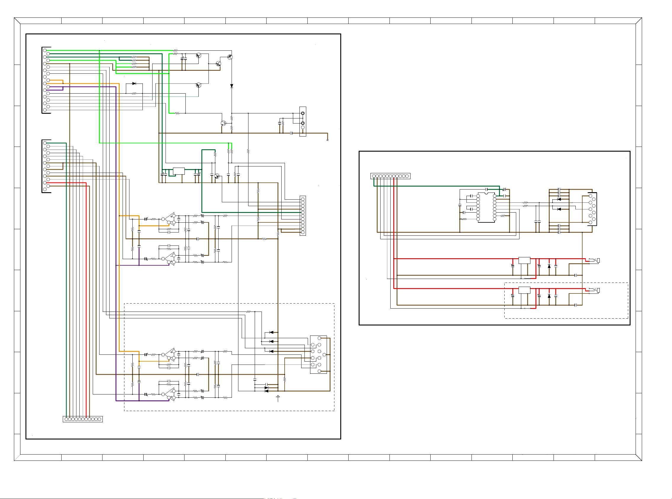
100
100K
R409
100K
R408
100K
R406
OPENC423 C420 OPEN
R430
10K
R426
4.7K
R425
4.7K
100K
R407
OPENC421
R429
10K
100N-C442
C422 OPEN
R403
OPEN(2W)
R401
OPEN(2W)
R417
10K
R416
10K
C416
OPEN
D404 OPEN
C404
100N-K
C408
10/50
C407
10/50
C406
10/50
C401
100N-K
D401
KDS160
R405
OPEN
R402
OPEN(2W)
R404
OPEN(2W)
43
2
1
IC401(1/2)
AZ4580MTR
R414
10K
C414
1000N-K
C413
OPEN
10K
R424
C418
OPEN
10K
R431
C417
OPEN
10K
R423
4.7K
R427
R428
4.7K
10K
R421
100N-K
C424
4700N-K
C470
C440 470P
100K
R437
C439 470P
R436
100K
C437
470P
100N-K
C436
R433
10K
KRC102S
Q404
R448
100
R445
220
R444
-
KDS160D402
D403 OPEN
D406
OPEN
D407
OPEN
R451
OPEN
R449
0
R459
OPEN
R452
47
100N-K
C446
C448
100N-K
100N-K
C450
C454
10/50
R456
1K
R455
1K
C457
10/50
ZD401
MTZ16B
100N-K
C469
JACK405
C403
100N-K
C402
100N-K
C405
10/50
43
2
1
IC402(1/2)
AZ4580MTR
5
678
IC401(2/2)
AZ4580MTR
R415
10K
R432
10K
10K
R422
C415
OPEN
C425
MQJO
C438 470P
100K
R435
KRC102S
Q403
100K
R434
100N-KC441
47ޓ
R446
R443
47K
D405
OPEN
R450
0
100N-K
C449
R453
1K
C455
10/50
C458
10/50
MTZ16B
ZD402
C459 33P
C456 33P
100N-K
C468
JACK406
54321
8967
JACK404
5
678
IC402(2/2)
AZ4580MTR
11 9
5
8
10
213
746
JACK402
C409 OPEN
C444 100N-K
100N-KC451
J438
C467 100N-K
C465 OPEN
C464
OPEN
C462
OPEN
R413
100
10/50
C434
C412 OPEN
R412
100
C411 OPEN
10/50
C433
10/50
C432
R411
100
C431
10/50
10/50
C430
C426
100N-K
10/50
C428
33K
R420
KRA102S
Q402
C419
OPEN
R418
100
100
R419
KRA102S
Q401
C443
470P
R440
470
R439
470
R460
OPEN
R438
470
R442
220
R447
JACK403
Q406
KRA102S
BKT401
C447
OPEN
R454
1K
C452
10/50
J437
ON/OFF
IN
GND
NC
OUT
PQ120DNA
IC406
C460
100N-K
ON/OFF
IN
GND
NC
OUT
PQ120DNA
IC405
C466 OPEN
D409 OPEN
D408
OPEN
C463
OPEN
54321 67891011
CP401
C435
10/50
C427
100N-K
R410
100
C410 OPEN
ON/OFF
IN
GND
NC
OUT
IC403
10/50
C429
R441
470
5432167891011
JACK401
C445
100N-K
KTC3875SYRTIKN
Q405
10 11 12 13 14 15 16
543216
9
87
IC404
ICL3232CVZ-T
R1 OUT
R1 IN
GND
VCC
T1 OUT
T1 IN
T2 IN
R2 OUTR2 IN
T2 OUT
V-
C2-
C2+
C1-
V+
C1+
C461
100N-K
108642
357
9
119
16 181412
11 13 1715
CN403
2
11311
141210
9753
864
15
CN402
C453
100N-K
5432167891011
CN401
AGND
AGND
+5VL
NC
REMOTE3.3V
D/MGND
232IMO
TRG2
TRG GND
NC
RC5
232OMI
TRG1
REMOTE3.3V
TRG +15V
TRG GND
TRG GND
M_XR
M_XL
SIRIUS_R
SIRIUS_L
TRG1
232OMI
RC_IN
BT_LINK
KILLIR
A-8V
A+8V
NC
SIRIUSMI
D/MGND
M3.3V
SWM5V(MX)
FARAME_GND
MXP_R
DETECT
7: A.GND
5: SIRIUS_R
3: SIRIUS_RX
1: NC
2: SIRIUS_RST
NC
NC
232OMI
NC
AGND
TRG +15V
TRG2
AGND
AGND
232IMO
REMOTE3.3V
RC_OUT
FRONT IRIN
A-8V
WAKEUP
SIRIUSRST
A+8V
D5V(MX)
SWM3.3V
SIRIUSMO
NC
NC
TRG +15V
TRG1
FARAME_GND
MXP_L
RC5_GND
+3.3V
SIRIUS
8: SIRIUS_L
6: SIRIUS_TX
4: GND
232IMO
TRG2
TRIGGER
OUT2
TRIGGER
OUT1
RS232C
PAGE 6(M3)PAGE 6(K3)
CNT B'D
D/MGND
CNT B'D
SIRIUS FARAME_GND
PAGE 8(I4)
RS232C B'D
PQ033DNA1ZPH
PAGE 8(B10)
SIRIUS B'D
SR7005 ONLY
U Model ONLY
REG_SIRIUS_COMMON CNT 4/4
SIRIUS/RS232C/TRIGGER
M-X PORT
RC-5
SCHEMATIC DIAGRAMS (8/37)
10
9
8
6
7
EDCBA HGF
2
3
4
5
FGH
1
ABCDE
4
5
2
3
MNOIJKL
1
LKI
J
MNO
7
6
8
9
10
C125Z1-19P
C125Z1-15P
s
 Loading...