

Service Manual
AV Surround Receiver
PS7002 /κιG AV Surround Amplifier

Please use this service manual with referring to the user guide (D.F.U.) without fail. 修理の際は、必ず取扱説明書を準備し操作方法を確認の上作業を行ってください。
marantz®
SR7002 / PS7002
Part no. 90M35CW855030 First Issue 2009.10
Copyright 2009 D&M Holdings Inc. All rights reserved. WARNING: Violators will be prosecuted to the maximum extent possible
MARANTZ DESIGN AND SERVICE
Using superior design and selected high grade components, MARANTZ company has created the ultimate in stereo sound. Only original MARANTZ parts can insure that your MARANTZ product will continue to perform to the specifications for which it is famous.
Parts for your MARANTZ equipment are generally available to our National Marantz Subsidiary or Agent.
ORDERING PARTS :
Parts can be ordered either by mail or by Fax.. In both cases, the correct part number has to be specified.
The following information must be supplied to eliminate delays in processing your order :
- 1. Complete address
- 2. Complete part numbers and quantities required
- 3. Description of parts
- 4. Model number for which part is required
- 5. Way of shipment
- 6. Signature : any order form or Fax. must be signed, otherwise such part order will be considered as null and void.
|
USA
MARANTZ AMERICA, INC 100 CORPORATE DRIVE MAHWAH, NEW JERSEY 07430 USA |
EUROPE / TRADING
D&M EUROPE B. V. P. O. BOX 8744, BUILDING SILVERPOINT BEEMDSTRAAT 11, 5653 MA EINDHOVEN THE NETHERLANDS PHONE : +31 - 40 - 2507844 FAX : +31 - 40 - 2507860 |
CANADA
D&M Canada Inc. 5-505 APPLE CREEK BLVD. MARKHAM, ONTARIO L3R 5B1 CANADA PHONE : 905 - 415 - 9292 FAX : 905 - 475 - 4159 |
|---|---|---|
|
JAPAN
D&M Holdings Inc. D&M BUILDING, 2-1 NISSHIN-CHO, KAWASAKI-KU, KAWASAKI-SHI, KANAGAWA, 210-8569 JAPAN |
株式会社 ディーアンドエムホールディングス
本 社 〒210-8569 神奈川県川崎市川崎区日進町2-1 D&Mビル |
KOREA
D&M SALES AND MARKETING KOREA LTD. CHUNG JIN B/D., #1001, 53-5, WONHYORO 3 GA, YONGSAN-GU, SEOUL, 140-719, KOREA PHONE : +82 - 2 - 323 - 2155 FAX : +82 - 2 - 323 - 2154 |
NOTE ON SAFETY :
Symbol A Fire or electrical shock hazard. Only original parts should be used to replaced any part marked with symbol A. Any other component substitution (other than original type), may increase risk of fire or electrical shock hazard.
安全上の注意:
▲ がついている部品は、安全上重要な部品です。必ず指定されている部品番号のものを使用して下さい。
SHOCK, FIRE HAZARD SERVICE TEST :
CAUTION : After servicing this appliance and prior to returning to customer, measure the resistance between either primary AC cord connector pins (with unit NOT connected to AC mains and its Power switch ON), and the face or Front Panel of product and controls and chassis bottom.
Any resistance measurement less than 1 Megohms should cause unit to be repaired or corrected before AC power is applied, and verified before it is return to the user/customer.
Ref. UL Standard No. 60065.
In case of difficulties, do not hesitate to contact the Technical Department at above mentioned address.
ROOM.808 SHANGHAI AIRPORT CITY TERMINAL NO.1600 NANJING (WEST) ROAD, SHANGHAI,
: 021 - 6248 - 5151 : 021 - 6248 - 4434
CHINA. 200040
TEL
1. TECHNICAL SPECIFICATIONS
| FM TUNER SECTION (Except PS7002) |
|---|
| Frequency Range |
| 87.5 - 108.0 MHz [ /N ] |
| 87.5 - 107.9 MHz [ /U ] |
| Usable SensitivityIHF 1.8 µV/16.4 dBf |
| Signal to Noise Ratio Mono/Stereo 75/70 dB |
| Distortion Mono/Stereo 0.2/0.3 % |
| Stereo Separation1 kHz 45 dB |
| Alternate Channel Selectivity ± 300 kHz 60 dB [ /F/N ] |
| ± 400 kHz 60 dB [ /U ] |
| Image Rejection |
| 98.1 MHz 70 dB [ /U ] |
| Tuner Output Level 1 kHz, ± 75 kHz Dev 800 mV |
AM TUNER SECTION (Except PS7002)
| 531 - 1602 kHz [ /F/N ] |
|---|
| 530 - 1710 kHz [ /U ] |
| 50 dB |
| Loop 400 µV [ /F/N ] |
| Loop 500 µV [ /U ] |
| 400Hz, 30 % Mod. 0.5 % |
| ± 20 kHz 70 dB |
| - |
HDMI SECTION
| Version | 1.3a [INPUT] |
|---|---|
| 1.3a [OUTPUT] |
DIMENSIONS


| Power Output (20 Hz - 20 kHz/THD=0.08%) | |
|---|---|
| Front L&R8 o | hms 110 W/Ch |
| Center | hms 110 W/Ch |
| Surround L&R8 o | hms 110 W/Ch |
| Surround Back L&R8 o | ohms 110 W/Ch |
| Front L&R 6 o | hms 140 W/Ch |
| Center 6 o | hms 140 W/Ch |
| Surround L&R 6 o | hms 140 W/Ch |
| Surround Back L&R 6 o | hms 140 W/Ch |
| Input Sensitivity/Impedance168 | mV/47 kohms |
| Signal to Noise Ratio | |
| Analog Input / Pure Direct | 105 dB |
| Frequency Response | |
| Analog Input / Pure Direct8 Hz - 10 | 0 kHz (± 3 dB) |
| Digital Input / 96 kHz PCM8 Hz - 4 | l5 kHz (± 3 dB) |
VIDEO SECTION
| Television Format | NTSC/PAL |
|---|---|
| Input Level/Impedance | 1 Vp-p/75 ohms |
| Output Level/Impedance | 1 Vp-p/75 ohms |
| Video Frequency Response | 5 Hz to 8 MHz (- 1 dB) |
| Video Frequency (Component) | . 5 Hz to 80 MHz (- 1 dB) |
| S/N | 60 dB |
GENERAL
| Power Requirement | AC 100 V 50/60 Hz [ /F ] | |
|---|---|---|
| AC 220 V 50 Hz [ /K ] | ||
| AC 230 V 50/60 Hz [ /N ] | ß | |
| AC 120 V 60 Hz [ /U ] | ||
| Power Consumption | ||
| 6.5 A [ /U ] | ||
| Weight | 15.0 kg (33.1 lbs) |
ACCESSORIES
| Remote Control Unit RC8001SR1 | |
|---|---|
| Remote Control Unit RC101 1 | |
| AAA-size batteries 5 | 5 |
| Microphone1 | |
| FM Antenna (Except PS7002)1 | |
| AM Loop Antenna (Except PS7002)1 | |
| Front AUX Jack Cover1 | |
| AC cable1 |

SURROUND MODE
This unit is equipped with many surround modes. These are provided to reproduce a variety of surround sound effects, according to the content of the source to be played.
The available surround modes may be restricted depending on the input signal and speaker setup.
The relationship between the selected surround mode and the input signal
The surround mode is selected with the surround mode selector on the unit or the remote controller. However, the sound you hear is subject to the relationship between the selected surround mode and the input signal. That relationship is as follows:
| 1 | Out | put Cha | annel | Front informatio | n display | ||||
|---|---|---|---|---|---|---|---|---|---|
| Surround Mode | Input Signal | Decoding | L/R | С |
SL
SR |
SBL
SBR |
SubW | Signal format indicators | Channel status |
| AUTO | Dolby Surr.EX | Dolby Digital EX | 0 | Ο | 0 | Ο | Ο | DIGITAL EX | L, C, R, SL, SR, S, LFE |
| Dolby D (5.1ch) | Dolby Digital 5.1 | 0 | 0 | 0 | - | 0 | L, C, R, SL, SR, LFE | ||
| Dolby D (2ch) | Dolby Digital 2.0 | 0 | - | - | - | 0 | L, R | ||
| Dolby D (2ch Surr) | Pro Logic IIx movie | 0 | 0 | 0 | 0 | 0 | L, R, S | ||
| Dolby Digital Plus (5.1ch) | DolbγDigital + | 0 | 0 | 0 | - | 0 | L, C, R, SL, SR, LFE | ||
| Dolby Digital Plus (6.1ch) | DolbyDigital + | 0 | 0 | 0 | 0 | 0 | L, C, R, SL, SR, S, LFE | ||
| Dolby Digital Plus (7.1) | DolbyDigital + | 0 | 0 | 0 | 0 | 0 | L, C, R, SL, SR, S, LFE | ||
| Dolby TrueHD (5.1ch) | DolbyTrueHD | 0 | 0 | 0 | - | 0 | Depend on speaker setup | ||
| Dolby TrueHD (6.1ch) | DolbyTrueHD | 0 | 0 | 0 | 0 | 0 | Depend on speaker setup | ||
| Dolby TrueHD (7.1ch) | DolbyTrueHD | 0 | 0 | 0 | 0 | 0 | Depend on speaker setup | ||
| DTS-ES | DTS-ES | 0 | 0 | 0 | 0 | 0 | dts, ES | L, C, R, SL, SR, S, LFE | |
| DTS 96/24 | DTS-96/24 | 0 | 0 | 0 | - | 0 | dts 96/24 | L, C, R, SL, SR, LFE | |
| DTS (5.1ch) | DTS 5.1 | 0 | 0 | 0 | - | 0 | dts | L, C, R, SL, SR, LFE | |
| DTS-HD (5.1) | DTS-HD | 0 | 0 | 0 | - | 0 | dts | L, C, R, SL, SR, LFE | |
| DTS-HD (6.1) | DTS-HD | 0 | 0 | 0 | Ο | 0 | dts | L, C, R, SL, SR, S, LFE | |
| DTS-HD (7.1) | DTS-HD | 0 | 0 | 0 | 0 | 0 | dts | L, C, R, SL, SR, S, LFE | |
| Multi Ch-PCM | Multi Ch-PCM | 0 | 0 | 0 | - | 0 | PCM | L, C, R, SL, SR, LFE | |
| Multi Ch-PCM 96kHz | Multi Ch-PCM 96kHz | 0 | 0 | Ο | - | 0 | PCM | L, C, R, SL, SR, LFE | |
| SA-CD (5.1ch) | Multi Ch-PCM | 0 | 0 | Ο | - | 0 | DSD | L, C, R, SL, SR, LFE | |
| SA-CD (2ch) | PCM (Stereo) | 0 | - | - | - | 0 | DSD | L, R | |
| PCM (Audio) | PCM (Stereo) | 0 | - | - | - | 0 | PCM | L, R | |
| PCM 96kHz | PCM (Stereo 96kHz) | 0 | - | - | - | 0 | PCM | L, R | |
| HDCD | HDCD | 0 | - | - | - | 0 | PCM, HDCD | L, R | |
| Analog | Stereo | 0 | - | - | - | 0 | ANALOG | - | |
| 7.1ch input | Multi Ch | 0 | 0 | 0 | 0 | 0 | ANALOG | - | |
| SOURCE DIRECT | Dolby Surr.EX | Dolby Digital EX | 0 | 0 | 0 | 0 | Ο | DIGITAL EX | L, C, R, SL, SR, S, LFE |
| PURE DIRECT | Dolby D (5.1ch) | Dolby Digital 5.1 | 0 | 0 | 0 | - | 0 | L, C, R, SL, SR, LFE | |
| Dolby D (2ch) | Dolby Digital 2.0 | 0 | - | - | - | 0 | L, R | ||
| Dolby D (2ch Surr) | Pro Logic IIx movie | 0 | 0 | Ο | Ο | 0 | L, R, S | ||
| Dolby Digital Plus (5.1) | DolbyDigital + | 0 | 0 | 0 | - | 0 | L, C, R, SL, SR, LFE | ||
| Dolby Digital Plus (6.1) | DolbyDigital + | 0 | 0 | 0 | Ο | 0 | L, C, R, SL, SR, S, LFE | ||
| Dolby Digital Plus (7.1) | DolbyDigital + | 0 | 0 | 0 | 0 | 0 | L, C, R, SL, SR, S, LFE | ||
| Dolby TrueHD (5.1) | DolbyTrueHD | 0 | 0 | 0 | - | 0 | Depend on speaker setup | ||
| Dolby TrueHD (6.1) | DolbyTrueHD | 0 | 0 | 0 | 0 | 0 | Depend on speaker setup | ||
| Dolby TrueHD (7.1) | DolbyTrueHD | 0 | 0 | 0 | 0 | 0 | Depend on speaker setup | ||
| DTS-ES | DTS-ES | 0 | 0 | 0 | Ο | 0 | dts, ES | L, C, R, SL, SR, S, LFE | |
| DTS 96/24 | DTS-96/24 | 0 | 0 | 0 | - | 0 | dts 96/24 | L, C, R, SL, SR, LFE | |
| DTS (5.1ch) | DTS 5.1 | 0 | 0 | 0 | - | 0 | dts | L, C, R, SL, SR, LFE | |
| DTS-HD (5.1) | DTS-HD | 0 | 0 | 0 | - | Ο | dts | L, C, R, SL, SR, LFE | |
| DTS-HD (6.1) | DTS-HD | 0 | 0 | 0 | 0 | 0 | dts | L, C, R, SL, SR, S, LFE | |
| DTS-HD (7.1) | DTS-HD | 0 | 0 | 0 | 0 | 0 | dts | L, C, R, SL, SR, S, LFE | |
| Multi Ch-PCM | Multi Ch-PCM | 0 | 0 | 0 | - | 0 | PCM | L, C, R, SL, SR, LFE | |
| Multi Ch-PCM 96kHz | Multi Ch-PCM 96kHz | 0 | 0 | 0 | - | 0 | PCM | L, C, R, SL, SR, LFE | |
| SA-CD (5.1ch) | SA-CD (5.1ch) | 0 | 0 | 0 | - | 0 | DSD | L, C, R, SL, SR, LFE | |
| SA-CD (2ch) | SA-CD (2ch) | 0 | - | - | - | 0 | DSD | L, R | |
| PCM (Audio) | PCM (Stereo) | 0 | - | - | - | - | PCM | L, R | |
| PCM 96kHz | PCM (Stereo 96kHz) | 0 | - | - | - | PCM | L, R | ||
| HDCD | HDCD | 0 | - | - | - | PCM, HDCD | L, R | ||
| Analog | Stereo | 0 | - | - | - | - | ANALOG | - | |
| 7.1ch input | Multi Ch | 0 | 0 | 0 | 0 | 0 | ANALOG | - | |
| EX/ES | Dolby Surr.EX | Dolby Digital EX | 0 | 0 | 0 | 0 | 0 | L, C, R, SL, SR, S, LFE | |
| Dolby D (5.1ch) | Dolby Digital EX | 0 | 0 | 0 | 0 | 0 | L, C, R, SL, SR, LFE | ||
| Dolby Digital Plus (5.1) | DolbyDigital + | 0 | 0 | 0 | 0 | 0 | L, C, R, SL, SR, LFE | ||
| Dolby TrueHD (5.1) | DolbyTrueHD | 0 | 0 | 0 | 0 | 0 | Depend on speaker setup | ||
| DTS-ES | DTS-ES | 0 | 0 | 0 | 0 | 0 | dts, ES | L, C, R, SL, SR, S, LFE | |
| DTS (5.1ch) | DTS-ES | 0 | 0 | 0 | 0 | 0 | dts | L, C, R, SL, SR, LFE | |
| Multi-PCM |
Multi Ch-PCM + Dolby
Digital EX |
0 | 0 | 0 | 0 | ο | PCM | L, C, R, SL, SR, LFE | |
| SA-CD (5.1ch) |
Multi Ch-PCM + Dolby
Digital EX |
0 | 0 | 0 | Ο | Ο | DSD | L, C, R, SL, SR, LFE |
| Out | out Cha | annel | Front informatio | n displav | |||||
|---|---|---|---|---|---|---|---|---|---|
| Surround Mode | Input Signal | Decoding | L/R | С |
SL
SR |
SBL
SBR |
SubW | Signal format indicators | Channel status |
| DOLBY | Dolby Surr.EX | Dolby Digital EX | 0 | 0 | 0 | - | 0 | L, C, R, SL, SR, S, LFE | |
| (PLIIx movie) | Dolby D (5.1ch) | Dolby Digital 5.1 | l õ | o | L, C, R, SL, SR, LFE | ||||
| Dolby D (5.1ch) | 18 | 8 | 8 | ||||||
| (PLIIX game) |
Dolby D (2ch)
Dolby D (2ch Surr) |
Pro Logic IIX
Pro Logic IIX |
HX |
H
|
H
|
H d | |||
| Dolby Digital Plus (5.1) | Hŏ | Hŏ | Hŏ |
н
С |
|||||
| Dolby Digital Plus (6.1) | DolbyDigital + | ŏ | ŏ | ŏ | Ο | ŏ | L.C.R.SL.SR.S.LFE | ||
| Dolby Digital Plus (7.1) | DolbyDigital + | ŏ | ŏ | ŏ | ŏ | ŏ | L.C.R.SL.SR.S.LFE | ||
| Dolby TrueHD (5.1) | DolbyTrueHD | 0 | 0 | 0 | - | 0 | Depend on speaker setup | ||
| Dolby TrueHD (6.1) | DolbyTrueHD | 0 | 0 | 0 | 0 | 0 | Depend on speaker setup | ||
| Dolby TrueHD (7.1) | DolbyTrueHD | 0 | 0 | 0 | 0 | 0 | Depend on speaker setup | ||
| Multi Ch-PCM | Multi Ch-PCM + PLIIx | l o | o | 0 | 0 | L, C, R, SL, SR, LFE | |||
| SA-CD (5.1ch) | Multi Ch-PCM + PLIIX | ||||||||
|
SA-UD (2ch)
DCM (Audio) |
Pro Logic IIX | 18 | |||||||
| HX | H | H | H | ||||||
| Analog | Нŏ | ŏ | Hŏ | ŏ | ŏ | _ _ n | |||
| DTS | DTS-FS | DTS 5 1 | ŏ | ŏ | ŏ | ŏ | dts FS | ||
| (Neo:6 Cinema) | DTS 96/24 | DTS-96/24 | ŏ | ŏ | ŏ | - | ŏ | dts 96/24 | L, C, R, SL, SR, LFE |
| (Neo:6 Music) | DTS (5.1ch) | DTS 5.1 | 0 | Ο | Ο | - | Ο | dts | L, C, R, SL, SR, LFE |
| `````````````````````````````````````` | DTS-HD(5.1) | DTS-HD | 0 | 0 | 0 | - | 0 | dts | L, C, R, SL, SR, LFE |
| DTS-HD(6.1) | DTS-HD | 0 | 0 | 0 | 0 | 0 | dts | L, C, R, SL, SR, S, LFE | |
| DTS-HD(7.1) | DTS-HD | 0 | 0 | 0 | 0 | 0 | dts | L, C, R, SL, SR, S, LFE | |
| Dolby D (2ch) | Neo:6 | | 0 | o | DO DIGITAL | |||||
| Dolby D (2ch Surr) | Neo:6 | l o | |||||||
| SA-CU (2ch) | Neo:6 | 18 | 8 | ||||||
| 18 | |||||||||
| Neo:6 | HĂ | HĂ | H | H | _ L, n | ||||
| CSTI Cinema | Dolby D (2ch) | CSIT | Ьŏ | ŏ | ŏ | ŏ | ŏ | ||
| CSII Music | Dolby D (2ch Surr) | CSII | Ō | ō | ō | ō | ŏ | L, R, S | |
| CSII Mono | SA-CD (2ch) | CSII | Ō | Ō | Ō | Ō | Ō | DSD | L, R |
| PCM (Audio) | CSII | 0 | Ο | Ο | Ο | Ο | PCM | L, R | |
| HDCD | CSII | 0 | 0 | 0 | 0 | 0 | PCM, HDCD | L, R | |
| Analog | CSII | 0 | 0 | 0 | 0 | ANALOG | - | ||
| STEREO | Dolby Surr.EX | Stereo | | 0 | • | - | • | o | ||
| Dolby D (5.1ch) | Stereo | · | - | · | |||||
|
Dolby D (2ch)
Dolby D (2ch Surr) |
Stereo | 18 | • | - | • |
L, K
L D S |
|||
| Dolby Digital Plus (51) | Steren | Ьŏ | - | ŏ | |||||
| Dolby Digital Plus (6.1) | Stereo | ŏ | - | - | - | ŏ | L, C, R, SL, SR, S, LFE | ||
| Dolby Digital Plus (7.1) | Stereo | Ō | - | - | - | ō | L. C. R. SL. SR. S. LFE | ||
| Dolby TrueHD (5.1) | Stereo | 0 | - | - | - | 0 | Depend on speaker setup | ||
| Dolby TrueHD (6.1) | Stereo | 0 | - | - | - | 0 | Depend on speaker setup | ||
| Dolby TrueHD (7.1) | Stereo | 0 | - | - | - | 0 | Depend on speaker setup | ||
| DTS-ES | Stereo | 0 | ŀ | - | · | 0 | dts, ES | L, C, R, SL, SR, S, LFE | |
| DIS 96/24 | Stereo | l O | · - | - | · | o | dts 96/24 | ||
| Stereo | 18 | • | - | • | dis | ||||
| Stereo | HX | · | - |
·
· |
K | dte | |||
| DTS-HD (0.1) | Steren | Ьŏ | - | ŏ | dis | ||||
| Multi Ch-PCM | Stereo | Ьŏ | - | ŏ | PCM | ||||
| Multi Ch-PCM 96kHz | Stereo | Ō | - | - | - | Ō | PCM | L, C, R, SL, SR, LFE | |
| SA-CD (5.1ch) | Stereo | 0 | - | - | - | 0 | DSD | L, C, R, SL, SR, LFE | |
| SA-CD (2ch) | Stereo | 0 | - | - | - | 0 | DSD | L, R | |
| PCM (Audio) | Stereo | 0 | • | - | • | 0 | PCM | L, R | |
| PCM 96kHz | Stereo | l o | • | - | • | 0 | L, R | ||
| Stereo | l Ö | - | - | - | |||||
| Dolby Virtual |
Analoq
Dolbu Surr EV |
Stereo
Delby Virtual Speaker |
18 | | · | - | · | |||
| Speaker | Dolby Surr.EX | Dolby Virtual Speaker | HX | - | • | • | |||
| opearei | Dolby Virtual Speaker | Ьŏ | - | ||||||
| Dolby D (2ch Surr) | Dolby Virtual Speaker | ŏ | - | LBS | |||||
| DTS-ES | Dolby Virtual Speaker | ŏ | - | - | - | - | dts. ES | L. C. R. SL. SR. S. LFE | |
| DTS 96/24 | Dolby Virtual Speaker | Ō | - | - | - | • | dts 96/24 | L, C, R, SL, SR, LFE | |
| DTS (5.1ch) | Dolby Virtual Speaker | 0 | - | - | - | - | dts | L, C, R, SL, SR, LFE | |
| Multi Ch-PCM | Dolby Virtual Speaker | 0 | - | - | - | - | PCM | L, C, R, SL, SR, LFE | |
| SA-CD (5.1ch) | Dolby Virtual Speaker | 0 | ŀ | - | ŀ | ŀ | DSD | L, C, R, SL, SR, LFE | |
| SA-CD (2ch) | Dolby Virtual Speaker | اڳ | | · | - | | · | ŀ | DSD | L, R | |
| PCM (Audio) | Dolby Virtual Speaker | اي | | · | - | | · | | · | |||
| Dolby Virtual Speaker | 분 | | · | - | · · | · · | ||||
| Multi Ch |
Analog
Dolby Surr EY |
Dolby Virtual Speaker | HX- |
·
( |
|||||
|
Movie
Movie |
Dolby D (5 1ch) | Dolby Digital EX | Ь | Ь | ـ | ŏ | |||
| Music | Dolby D (2ch) | Multi Channel | Ιŏ | ю | ŏ | 0 | ŏ | L, R | |
| (O): Movie mode only. | Dolby D (2ch Surr) | Multi Channel | 0 | (0) | 0 | Ο | Ο | DIGITAL DI SURROUND | L, R, S |
| Output Channel | Front information display | |||||||||
|---|---|---|---|---|---|---|---|---|---|---|
| Surround Mode | Input Signal | Decoding | SL | SBL | ||||||
| L/R | C | SR | SBR | SubW | Signal format indicators | Channel status | ||||
| Multi Ch | dte ES | |||||||||
|
Movie
Movie |
DTS-96/24 | НĂ- |
|
|
|
dts, 20
dts 96/24 |
||||
| Music | DTS (5.1ch) | H d |
|
|
dis 50/24
dte |
|||||
| IVIUSIC | Multich DCM | H۲- | HXX |
|
|
|||||
| Multi Ch. DCM 06kU+ | HX- | HX- | HX- | |||||||
| H۲- |
|
- |
|
|||||||
| SA-CD (S. run) | Multi Channel | HX- | HX- | HX- | ||||||
| Multi Chappal | H۲. |
|
|
H × | DOD | |||||
| Multi Channel | H۲- | HX: |
|
|
|
|||||
| (O): Movie mode only | Multi Channel | 8 | HX- | 18- | HX- | |||||
| Delley LLD |
Analog
Dalby Sum EV |
18- | 10 | |||||||
| рору н.е | Dolby Surr.EX | 18 | - | - | - | - | ||||
| · · | · · | - | - | |||||||
| ŀ | | · | - | - | |||||||
| · - | ŀ | - | - | |||||||
| Dolby Digital Plus (5.1) | Stereo | - | - | - | v | |||||
| Dolby Digital Plus (6.1) | Stereo | - | - | - | L, C, R, SL, SR, S, LFE | |||||
| Dolby Digital Plus (7.1) | Stereo | 0 | ŀ | · · | - | 0 | L, C, R, SL, SR, S, LFE | |||
| Dolby TrueHD (5.1) | Stereo | ŀ | ŀ | - | o | Depend on speaker setup | ||||
| Dolby TrueHD (6.1) | Stereo | · . | · . | - | 0 | Depend on speaker setup | ||||
| Dolby TrueHD (7.1) | Stereo | 0 | ŀ | ŀ | - | 0 | Depend on speaker setup | |||
| DTS-ES | Dolby H.P | Q | - | - | - | - | dts, ES | L, C, R, SL, SR, S, LFE | ||
| DTS 96/24 | Dolby H.P | 0 | - | - | - | - | dts 96/24 | L, C, R, SL, SR, LFE | ||
| DTS (5.1ch) | Dolby H.P | 0 | · | - | - | - | dts | L, C, R, SL, SR, LFE | ||
| DTS-HD (5.1) | Stereo | 0 | ŀ | - | - | 0 | dts | L, C, R, SL, SR, LFE | ||
| DTS-HD (6.1) | Stereo | - | - | 0 | dts | L, C, R, SL, SR, S, LFE | ||||
| DTS-HD (7.1) | Stereo | 0 | - | - | - | 0 | dts | L, C, R, SL, SR, S, LFE | ||
| Multi Ch-PCM | Dolby H.P | 0 | • | - | - | - | PCM | L, C, R, SL, SR, LFE | ||
| SA-CD (5.1ch) | Dolby H.P | 0 | - | - | - | - | DSD | L, C, R, SL, SR, LFE | ||
| SA-CD (2ch) | Dolby H.P | 0 | - | - | - | - | DSD | L, R | ||
| PCM (Audio) | Dolby H.P | 0 | - | - | - | - | PCM | L, R | ||
| HDCD | Dolby H.P | 0 | - | - | - | - | PCM, HDCD | L, R | ||
| Analog | Dolby H.P | 0 | • | - | - | - | ANALOG | - | ||
| ТНХ | Dolby Surr.EX | Dolby Digital + THX Surround EX | 0 | 0 | 0 | 0 | 0 | DIGITAL EX | L, C, R, SL, SR, S, LFE | |
| (AUTO) | Dolby D (5.1ch) | Dolby Digital 5.1+ THX 5.1 | 0 | 0 | 0 | - | 0 | L, C, R, SL, SR, LFE | ||
| Dolby D (2ch) | Pro Logic IIx movie + THX | Ο | Ο | Ο | Ο | 0 | L, R | |||
| Dolby D (2ch Surr) | Pro Logic IIx movie + THX | Ο | Ο | 0 | 0 | 0 | L, R, S | |||
| DTS-ES | DTS-ES + THX | 0 | Ο | Ο | Ο | Ο | dts, ES | L, C, R, SL, SR, S, LFE | ||
| DTS (5.1ch) | DTS + THX 5.1 | Ο | Ο | Ο | - | Ο | dts | L, C, R, SL, SR, LFE | ||
| Multi Ch-PCM | Multi Ch-PCM + THX5.1 | 0 | 0 | 0 | - | 0 | PCM | L, C, R, SL, SR, LFE | ||
| SA-CD (5.1ch) | Multi Ch-PCM + THX5.1 | 0 | 0 | 0 | - | 0 | DSD | L, C, R, SL, SR, LFE | ||
| SA-CD (2ch) | Pro Logic IIx movie + THX | 0 | 0 | 0 | 0 | 0 | DSD | L.R | ||
| PCM (Audio) | Pro Logic IIx movie + THX | 0 | 0 | 0 | 0 | 0 | PCM | L.R | ||
| HDCD | Pro Logic IIx movie + THX | Ō | Ō | Ō | Ō | Ō | PCM, HDCD | L.R | ||
| Analog | Pro Logic IIx movie + THX | 0 | Ō | Ō | Ō | 0 | ANALOG | - | ||
| THX Select2 | Dolby Surr.EX | Dolby Digital + THX Surround EX | Ō | Ō | Ō | Ō | Ō | DO DIGITAL EX | L. C. R. SL. SR. S. LFE | |
| (THX EX) | Dolby D (5.1ch) | Dolby Digital 5.1+ THX | Ō | Ō | Ō | Ō | Ō | L C B SL SB LFE | ||
| (THX Cinema) | Boildy B (b. rony | Select2 Cinema | Ĭ | Ĭ | Ĭ | ľ | Ĭ | |||
| (THX Music) | Dolby D (2ch) | 0 | 0 | 0 | 0 | 0 | I B | |||
| (THX Games) | Dolby D (2ch Surr) | ŏ | ŏ | ŏ | ŏ | ŏ | I B S | |||
| DTS-ES | ŏ | ŏ | ŏ | ŏ | ŏ | dts ES | ||||
| DTS (5.1ch) | DTS + THX Select2 Cinema | ŏ | ŏ | ŏ | ŏ | ŏ | dts | |||
| Multi Ch-PCM | Multi Ch-PCM + THX | ŏ | ŏ | ŏ | ŏ | ŏ | PCM | |||
| Select2 Cinema | ľ | ľ | ١Ŭ | ١Ŭ | ||||||
| SA-CD (5.1cb) | ||||||||||
| 5A-00 (5.101) | Select2 Cinema | Ľ | Ľ | l 🗸 | 000 | |||||
| SA-CD (2ch) |
Deleciz Offerna
Dro Logio II y movio - TUV |
|||||||||
| H۲- | 片 | 片 | ⊢≻ | H۲- | DOD | |||||
| ⊢∺ | 片 | 片 | HX- |
|
||||||
| H۲. | H۲. | H۲. |
|
LX- | ||||||
| Analog | I U - | I U - | ANALUG | 1 - I | ||||||
Notes:
- Dolby Digital (2 channel L/R): Speakers for signal with Dolby Surround are fully equipped.
- No sound is outputs from the surround speaker, center speaker and subwoofer if the DVD disc has no surround data.
- Surround modes other than Stereo are not available during Dolby TrueHD, Dolby Digital Plus, or DTS-HD playback.
If surround modes other than Stereo are selected and Dolby TrueHD, Dolby Digital Plus, or DTS-HD content is played, the surround mode setting is disabled.
Abbreviations
L/R : Front speakers
C : Center speaker
- SL/SR : Surround speakers
-
SBL/SBR : Surround back speakers
- SubW : Subwoofer
2. TECHNICAL DESCRIPTION
DESCRIPTION
THX® is an exclusive set of standards and technologies established by the world-renowned film production company, Lucasfilm Ltd. THX resulted from George Lucas' desire to reproduce the movie soundtrack as faithfully as possible both in the movie theater and in the home theater.
THX engineers developed patented technologies to accurately translate the sound from a movie theater environment into the home, correcting the tonal and spatial errors that occur.
When the THX mode of the unit is on, three distinct THX technologies are automatically added:
Re-Equalization-restores the correct tonal balance for watching a movie in a home environment.
These sounds are otherwise mixed to be brighter for a large movie theater. Re-EQ compensates for this and prevents the soundtracks from being overly bright and harsh when played in a home theater.
Timbre Matching-filters the information going to the surround speakers so they more closely match the tonal characteristics of the sound coming from the front speakers.
This ensures seamless panning between the front and surround speakers.
Adaptive Decorrelation-slightly changes one surround channel's time and phase relationship with respect to the other surround channel.
This expands the listening position and creates with only two surround speakers the same spacious surround experience as in a movie theater with multiple surround speakers.
The unit was required to pass a rigorous series of quality and performance tests, in addition to incorporating the technologies explained above, in order to be THX certified.
THX requirements cover every aspect of performance including pre-amplifier and power amplifier performance and operation, and hundreds of other parameters in both the digital and analog domain.
Movies which have been encoded in Dolby Digital, DTS, Dolby Pro Logic, stereo and Mono will all benefit from the THX mode when being viewed.
The THX mode should only be activated when watching movies which were originally produced for a movie theater environment.
THX need not be activated for music, movies made especially for TV, or shows such as sports programming, talk shows, etc.
This is because they were originally mixed for a small room environment.
THX and Select 2 are trademarks of THX Ltd. THX may be registered in some jurisdictions. Surround EX is a trademark of Dolby Laboratories. Used with permission.
THX SURROUND EX
THX Surround EX—Dolby Digital Surround EX is a joint development of Dolby Laboratories and THX Ltd.
In a movie theater, film soundtracks that have been encoded with Dolby Digital Surround EX technology are able to reproduce an extra channel which has been added during the mixing of the program. This channel, called Surround Back, places sounds behind the listener in addition to the currently available front left, front center, front right, surround right, surround left and subwoofer channels. This additional channel provides the opportunity for more detailed imaging behind the listener and brings more depth, spacious ambience and sound localization than ever before.
Movies that were created using the Dolby Digital Surround EX technology, when released into the home consumer market may exhibit wording to that effect on the packaging. A list of movies created using this technology can be found on the Dolby web site at www.dolby.com. A list of available DVD software titles encoded with this technology an be found at www.thx.com.
Only receiver and controller products bearing the THX Surround EX logo, when in the THX Surround EX mode, faithfully reproduce this new technology in the home. This product may also engage the THX Surround EX mode during the playback of 5.1 channel material that is not Dolby Digital Surround EX eocnded. In such case, the information delivered to the Surround Back channel will be program dependent and may or may not be very pleasing depending on the particular soundtrack and the tastes of the individual listener.
"SURROUND EX™" is a trademark of Dolby Laboratories. Used under authorization.
THX Select2
Before any home theater component can be THX Select2 certified, it must pass a rigorous series of quality and performance tests. Only then can a product feature the THX Select2 logo, which is your guarantee that the Home Theater products you purchase will give you superb performance for many years to come. THX Select2 requirements define hundreds of parameters, including power amplifier performance, and pre-amplifier performance and operation for both digital and analog domains. THX Select2 receivers also feature proprietary THX technologies (e.g., THX Mode) which accurately translate movie soundtracks for home theater playback.

Neural Surround™, THX® Technologies has been chosen as the official surround sound broadcast format for XM Satellite Radio's "XM HD Surround" and other leading FM/HD radio stations in the USA and worldwide. Neural Surround, THX Technologies delivers the rich envelopment and discrete image detail of surround sound in a format 100% compatible with stereo.
Neural Surround, THX Technologies draws the brain's attention to sonic details in musical instruments, vocals and ambience that are typically masked by other playback systems. This allows the listener to fully experience the richness and subtleties in recorded performance as never before for both surround encoded material and regular stereo material such as CDs or digital media players. Neural Surround, THX Technologies is enabling the second surround sound revolution, bringing surround directly to your ears!
This product is manufactured under license from Neural Audio Corporation and THX Ltd. Marantz hereby grants the user a non-exclusive, nontransferable, limited right of use to this product under USA and foreign patent, patent pending and other technology or trademarks owned by Neural Audio Corporation and THX Ltd. "Neural Surround", "Neural Audio", "Neural" and "NRL" are trademarks and logos owned by Neural Audio Corporation, THX is a trademark of THX Ltd., which may be registered in some jurisdictions. All rights reserved.

Manufactured under license under U.S. Patent #'s: 5,451,942; 5,956,674; 5,974,380; 5,978,762; 6,226,616; 6,487,535; 7,003,467 & other U.S. and worldwide patents issued & pending. DTS, DTS Digital Surround, ES, and Neo:6 are registered trademarks and the DTS logos, Symbol and DTS 96/24 are trademarks of DTS, Inc. © 1996-2007 DTS, Inc. All Rights Reserved.
• dts Digital Surround
DTS was introduced in 1994 to provide 5.1 channels of discrete digital audio into home theater systems.
DTS brings you premium quality discrete multichannel digital sound to both movies and music.
DTS is a multichannel sound system designed to create full range digital sound reproduction.
The no compromise DTS digital process sets the standard of quality for cinema sound by delivering an exact copy of the studio master recordings to neighborhood and home theaters.
Now, every moviegoer can hear the sound exactly as the moviemaker intended.
DTS can be enjoyed in the home for either movies or music on of DVD's, LD's, and CD's.
• dts Neo:6®
The advantages of discrete multichannel systems over matrix are well known.
But even in homes equipped for discrete multichannel, there remains a need for high-quality matrix decoding. This is because of the large library of matrix surround motion pictures available on disc and on VHS tape; and analog television broadcasts.
The typical matrix decoder of today derives a center channel and a mono surround channel from twochannel matrix stereo material. It is better than a simple matrix in that it includes steering logic to improve separation, but because of its mono, bandlimited surround it can be disappointing to users accustomed to discrete multichannel.
Neo:6 offers several important improvements as follow,
- Neo:6 provides up to six full-band channels of matrix decoding from stereo matrix material. Users with 6.1 and 5.1 systems will derive six and five separate channels, respectively, corresponding to the standard home-theater speaker layouts.
- Neo:6 technology allows various sound elements within a channel or channels to be steered separately, and in a way which follows naturally from the original presentation.
- Neo:6 offers a music mode to expand stereo nonmatrix recordings into the five- or six-channel layout, in a way which does not diminish the subtlety and integrity of the original stereo recording.
• dts Digital Surround ES®
DTS-ES Extended Surround is a new multichannel digital signal format developed by Digital Theater Systems Inc. While offering high compatibility with the conventional DTS Digital Surround format, DTS-ES Extended Surround greatly improves the 360degree surround impression and space expression thanks to further expanded surround signals. This format has been used professionally in movie theaters since 1999.
In addition to the 5.1 surround channels (FL, FR, C, SL, SR and LFE), DTS-ES Extended Surround also offers the SB (Surround Back) channel for surround playback with a total of 6.1 channels. DTS-ES Extended Surround includes two signal formats with different surround signal recording methods, as DTS-ES Discrete 6.1 and DTS-ES Matrix 6.1.
• dts Digital Surround 96/24
The stereo CD is a 16-bit medium with sampling at 44.1 kHz. Professional audio has been 20- or 24bit for some time, and there is increasing interest in higher sampling rates both for recording and for delivery into the home. Greater bit depths provide extended dynamic range. Higher sampling rates allow wider frequency response and the use of antialias and reconstruction filters with more favorable aural characteristics.
DTS 96/24 allows for 5.1 channel sound tracks to be encoded at a rate of 96kHz/24bits on DVD-Video titles.
When DVD-video appeared, it became possible to deliver 24-bit, 96 kHz audio into the home, but only in two channels, and with serious limitations on picture. This capability has had little use.
DVD-audio allows 96/24 in six channels, but a new player is needed, and only analog outputs are provided, necessitating the use of the D/A converters and analog electronics provided in the player.
- DTS 96/24 offers the following:
- 1. Sound quality transparent to the original 96/24 master.
- 2. Full backward compatibility with all existing decoders. (Existing decoders will output a 48 kHz signal)
- 3. No new player required: DTS 96/24 can be carried on DVD-video, or in the video zone of DVD-audio, accessible to all DVD players.
- 4.96/24 5.1-channel sound with full-quality fullmotion video, for music programs and motion picture soundtracks on DVD-video.

DTS-HD Master Audio is capable of delivering audio that is a bit-for-bit identical to the studio master. DTS-HD Master Audio delivers audio at super high variable bit rates -24.5 mega-bits per second (Mbps) on Blu-ray discs and 18.0 Mbps on HD-DVD - that are significantly higher than standard DVDs . This bit stream is so "fast" and the transfer rate is so "high" that it can deliver the Holy Grail of audio: 7.1 audio channels at 96k sampling frequency/24 bit depths that are identical to the original. With DTS-HD Master Audio, you will be able to experience movies and music, exactly as the artist intended: clear, pure, and uncompromised.
Manufactured under license under U.S. Patent #'s: 5,451,942; 5,956,674; 5,974,380; 5,978,762; 6,226,616; 6,487,535 & other U.S. and worldwide patents issued & pending. DTS is a registered trademark & the DTS logos and Symbol are trademarks of DTS, Inc. © 1996-2007 DTS, Inc. All Rights Reserved.

DTS-HD High Resolution Audio can deliver up to 7.1 channels of sound that is virtually indistinguishable from the original. DTS-HD High Resolution Audio delivers audio at high constant bit rates superior to standard DVDs---6.0 Mbps on Blu-ray discs and 3.0 Mbps on HD-DVD to produce outstanding sound quality. It is capable of delivering up to 7.1 channels at 96k sampling frequency/24 bit depth resolution. It allows content creators to deliver rich, high definition audio on movies where disc space may not allow for DTS-HD Master Audio.
Manufactured under license under U.S. Patent #'s: 5,451,942; 5,956,674; 5,974,380; 5,978,762; 6,226,616; 6,487,535 & other U.S. and worldwide patents issued & pending. DTS is a registered trademark and the DTS logos, Symbol, DTS-HD, DTS-HD High Resolution
Audio and DTS-HD High Res Audio are trademarks of DTS, Inc. © 1996-2007 DTS, Inc. All Rights Reserved.

Dolby Digital identifies the use of Dolby Digital audio coding for such consumer formats as DVD and DTV. As with film sound, Dolby Digital can provide up to five full-range channels for left, center, and right screen channels, independent left and right surround channels, and a sixth (".1") channel for lowfrequency effects.
Dolby Surround Pro Logic II is an improved matrix decoding technology that provides better spatiality and directionality on Dolby Surround program material; provides a convincing three-dimensional soundfield on conventional stereo music recordings; and is ideally suited to bring the surround experience to automotive sound. While conventional surround programming is fully compatible with Dolby Surround Pro Logic II decoders, soundtracks will be able to be encoded specifically to take full advantage of Pro Logic II playback, including separate left and right surround channels. (Such material is also compatible with conventional Pro Logic decoders.)
Dolby Digital EX creates six full-bandwidth output channels from 5.1-channel sources. This is done using a matrix decoder that derives three surround channels from the two in the original recording. For best results, Dolby Digital EX should be used with movies soundtracks recorded with Dolby Digital Surround EX.
About Dolby Pro Logic II x
Dolby Pro Logic IIx technology delivers a natural and immersing 7.1-channel listening experience to the home theater environment. A product of Dolby's expertise in surround sound and matrix decoding technologies, Dolby Pro Logic IIx is a complete surround sound solution that maximizes the entertainment experience from stereo as well as 5.1-channel encoded sources.
Dolby Pro Logic IIx is fully compatible with Dolby Surround Pro Logic technology and can optimally decode the thousands of commercially available Dolby Surround encoded video cassettes and television programs with enhanced depth and spatiality. It can also process any high-quality stereo or Advanced Resolution 5.1-channel music content into a seamless 6.1- or 7.1-channel listening experience.

The Dolby Headphone technology provides a surround sound listening experience over headphones. When listening to multichannel content such as DVD movies over headphones, the listening experience is fundamentally different than listening to speakers. Since the headphone speaker drivers are covering the pinna of the ear, the listening experience differs greatly from traditional speaker playback. Dolby utilizes patented headphone perspective curves to solve this problem and provides a non-fatiguing, immersive, home theater listening experience. Dolby Headphone also delivers exceptional 3D audio from stereo material.
Dolby Virtual Speaker is a technologycertified by Dolby Laboratories that creates a virtualized surround sound experience from two speakers using a multichannel Dolby Digital source. Additionally, Dolby Virtual Speaker can simulate the surround sound effect produced by Dolby Pro Logic or Dolby Pro Logic II.
Dolby Virtual Speaker retains all the original Multichannel audio information and provides the listener with the sensation of being surrounded by additional speakers.
Manufactured under license from Dolby Laboratories. "Dolby", "Pro Logic", "Surround EX", and the double-D symbol are trademarks of Dolby Laboratories.
Dolby® TrueHD is Dolby's next-generation lossless technology developed for high-definition disc-based media. Dolby TrueHD delivers tantalizing sound that is bit-for-bit identical to the studio master, unlocking the true high-definition entertainment experience on next-generation discs. When coupled with high-definition video, Dolby TrueHD offers an unprecedented home theater experience that lets you enjoy sound as stunning as the high-definition picture.
Manufactured under license from Dolby Laboratories. "Dolby", "Pro Logic", "Surround EX", and the double-D symbol are trademarks of Dolby Laboratories.
Dolby Digital Plus is a highly sophisticated and
versatile audio codec based on Dolby Digital and designed specifically to adapt to the changing demands of future audio, video delivery, and audio storage systems while simultaneously retaining backwards compatibility with the existing Dolby Digital 5.1-channel home theater systems in use today.
Manufactured under license from Dolby Laboratories. "Dolby", "Pro Logic", "Surround EX", and the double-D symbol are trademarks of Dolby Laboratories.

Circle Surround II (CS-II) is a powerful and versatile multichannel technology. CS-II is designed to enable up to 6.1 multichannel surround sound playback from mono, stereo, CS encoded sources and other matrix encoded sources. In all cases the decoder extends it into 6 channels of surround audio and a LFE/subwoofer signal. The CS-II decoder creates a listening environment that places the listener "inside" music performances and dramatically improves both hi-fi audio conventional surround-encoded video material. CS-II provides composite stereo rear channels to greatly improve separation and image positioning– adding a heightened sense of realism to both audio and A/V productions.
CS-II is packed with other useful feature like dialog clarity (SRS Dialog) for movies and cinema-like bass enrichment (TruBass). CS-II can enable the dialog to become clearer and more discernable in movies and it enables the bass frequencies contained in the original programming to more closely achieve low frequencies—overcoming the low frequency limitations of the speakers by full octave.
Circle Surround II, Dialog Clarity, TruBass, SRS and symbol are trademarks of SRS Labs, Inc.
Circle Surround II, Dialog Clarity and TruBass technology are incorporated under license from SRS Labs, Inc.

HDCD® (High Definition Compatible Digital ®) is a patented process for delivering on Compact Disc the full richness and details of the original microphone feed.
HDCD encoded CDs sound better because they are encoded with 20-bits of real musical information as compared to 16-bits for all other CDs.
HDCD overcomes the limitation of the 16-bit CD format by using a sophisticated system to encode the additional four bits onto the CD while remaining completely compatible with the CD format.
When listening to HDCD recordings, you hear more dynamic range, a focused 3-D sound stage, and extremely natural vocal and musical timbre. With HDCD, you get the body, depth and emotion of the original performance not a flat, digital imitation.
HDCD system manufactured under license from Microsoft. This product is covered by one or more of the following: In the United States 5,479,168 5,638,074 5,640,161 5,808,574 5,838,274 5,854,600 5,864,311 5,872,531 and in Australia 669,114 with other patents pending.
HDMI
HDMI, the HEDMI and High-Definition Multimedia Interface are trademarks or registered trademarks of HDMI Licensing LLC.
XM Satellite Radio Ready

READY
The XM name and related logos are registered trademarks of XM Satellite Radio Inc.
XM HD Surround uses Neural Surround™ technology to achieve optimal surround sound from XM radio.
There are several factors that can degrade the sound from even the best loudspeakers in a listening room. One of the most important is the interaction of sound from the loudspeakers with large surfaces such as walls, the floor, and the ceiling in the room. Even with careful loudspeaker placement and acoustical treatments, there are significant problems that are caused by room acoustics. These include reflections from nearby surfaces and standing waves that are created between large parallel surfaces in the room. In a home theater the situation is further complicated because there are several listening locations. The effects of room acoustics on the sound arriving at each person's ears are very different and the result is a listening experience that is degraded in a different way for every person in the room. It is not uncommon to have variations in two adjacent seats that are as large as 10 dB, particularly in the frequency range below 250 Hz
The solution to this problem is to apply room correction after precisely measuring how each loudspeaker interacts with the room. Because the room causes variations in the frequency response of the loudspeakers that are so large from seat to seat, it is important to measure each loudspeaker at several locations in the listening room. This should be done even if there is only one listener. Measurement at a single location is not representative of the acoustical problems in the room and will in most cases, degrade overall performance. Audyssev MultEQ is the only technology that can achieve room correction for multiple listeners in a large listening area. It does so by combining the data collected at several points in the room from each loudspeaker and then applying correction that minimizes the acoustical effects of the room and is matched to the frequency resolution of human perception (known as psychoacoustics). Furthermore, MultEQ correction is applied both in frequency and time domains and so there are no artifacts (such as smearing of sound or modal ringing)that are sometimes associated with traditional methods of room equalization.
In addition to correcting frequency response problems over a wide listening area, Audyssey MultEQ provides a completely automated sound system set-up process. It identifies how many loudspeakers are connected to the amplifiers and whether they are fullrange, satellites, or subwoofers. If there is a least one subwoofer connected, Audyssey MultEQ determines the optimum crossover frequency between each satellite and the subwoofer(s). It automatically checks the polarity of each loudspeaker and alerts the user if there are any that may be wired outof-phase relative to the others. It measures the distance to each loudspeaker from the main listening position and adjusts the delays so that sound from each loudspeaker arrives at the same time. Finally, Audyssev MuitEQ determines the playback level of each loudspeaker and adjusts the volume trims so that all levels are equal.

MultEQ and the Audyssey MultEQ logo are trademarks of Audyssey Laboratories, Inc. All rights reserved.
3. POWER AMPLIFIER ADJUSTMENT
Idling Current Alignment
- 1. Each of the measurement points are provided with the two test points. Set a digital Voltage meter to DC voltage input, connect the meter to the test points at both contact points.
- 2. After the setup above, turn on the main switch.
- 3. Adjust variable resistors (VR41 VR71) according to the digital voltmeter readings. The target setting value is the following table for each channel.
Settings: Master Volume — Minimum
Speaker out — No Load Top lid
— OPEN
アイドリング雷流調整
- 1. 電源を ON する前にそれぞれの "+" 端子と "-" 端子間にデ ジタルボルトメーターを接続します。デジタルボルトメー ターを DC 電圧入力にセットします。
- 2. 上記のセットアップの後に、本機の電源を ON します。
- 3. デジタルボルトメーターの電圧値を監視しながら可変抵抗 器 (VR41 ~ VR71) を調節します。 各チャンネルの目標値は下記の表を参照下さい。
セッティング:マスター・ボリューム — 最小 スピーカー接続 ― 無し --- 無し
| Channel | Alignment Point | Measurement Point |
|---|---|---|
| Front L | VR41 | CN41 |
| Center | VR61 | CN61 |
| Front R | VR51 | CN51 |
| Surround L | VR42 | CN42 |
| Surround R | VR52 | CN52 |
| Surround Back L | VR62 | CN62 |
| Surround Back R | VR71 | CN71 |
Time Table of Idling Current Rise
| Ambient temperature | ||||||
|---|---|---|---|---|---|---|
| After Turning ON | 20 to 30 degrees centigrade | |||||
| Measurement Voltage | ||||||
| 10 min. | 2.4 mV ± 0.3 mV | |||||
| 20 min. | 2.4 mV ± 0.3 mV | |||||
| 30 min. | 2.4 mV ± 0.3 mV | |||||
4. SERVICE MODE
MAIN CPU Version, DSP Version, HDMI CPU Version and Seament Check Mode.
- 1 Connect the mains cord into the unit
- 2. Press the POWER ON/STANDBY button for turn on the unit
- 3 Press the PURE DIRECT . 7.1CH INPUT and M-DAX buttons simultaneously more then 3 seconds.
- 4. The EL display shows "SERVICE MODE" for 2 seconds then shows the model name
| S | E | R | V | Ι | С | Ε | Μ | Ο | D | Ε | ||
|---|---|---|---|---|---|---|---|---|---|---|---|---|
| S | R | 7 | 0 | 0 | 2 | |||||||
| Р | S | 7 | 0 | 0 | 2) | |||||||
5. Press the ENTER button, the software version of the MAIN CPU (IC17) is displayed in the format below.
| V | 0 | 7 | 0 | 8 | 0 | 4 | 1 | U | ||||
|---|---|---|---|---|---|---|---|---|---|---|---|---|
| Lγε | ar⊥ |
|
Mo |
nth | | Da | ate 🗌 | Re |
|
lease |
⊨
∋ No. |
De | stina | tion |
unit is displayed.
| Μ | Ζ | 2 | 9 | 4 | 9 | 6 | 7 | 2 | 9 | 5 |
|---|
7. Press the ENTER button, the software version of the TI DSP (IC34) B1 Code is displayed in the format below.
| В | 1 | 1 | 0 | 7 | 0 | 7 | 0 | 5 | 1 | ||
|---|---|---|---|---|---|---|---|---|---|---|---|
| 1 | 1 | 1 | 1 | 1 |
8. Press the ENTER button, the software version of the TI DSP (IC34) B2 Code is displayed in the format below.
| В | 2 | 1 | 0 | 7 | 0 | 7 | 0 | 5 | 1 |
|---|
9. Press the ENTER button, the software version of the HDMI CPU (IC81) is displayed in the format below.
| Н | D | М | Ι | V | е | r | h | 2 | 1 |
|---|
- 10. Press the ENTER button again, the left half, right half and center of the label area in the FLD light on and off each other.
- 11. Press the ENTER button again, the segments of the character area in the FLD flick in checker pattern.
- 12. Press the ENTER button again, all the FL segments turns off.
- 13. Press the ENTER button again to guit this mode.
4. SERVICE MODE
MAIN CPU Version, DSP Version, HDMI CPU Version and Seament Check Mode.
- 1. 本機に電源コードを接続します。
- 2. POWER ON/STANDBYボタンを押し、本機の電源を入れ ます。
- 3. PURE DIRECT. 7.1CH INPUT. M-DAXの3つのボタンを 同時に3秒以上押します。
- 4. FLに"SERVICE MODE"と2秒表示し、次にモデル名を表 示します。
| S | Е | R | V | Ι | С | Е | М | 0 | D | Е | |
|---|---|---|---|---|---|---|---|---|---|---|---|
5. ENTERボタンを押すと、MAINマイコン(IC17)のバージョ ンが表示されます。
| V | 0 | 7 | 0 | 8 | 0 | 4 | 1 | U | |||
|---|---|---|---|---|---|---|---|---|---|---|---|
| LYe | ear – | Mo | nth ] | Da | ate - | יע |
|
リーフ |
ー
ス No |
可け |
6. Press the ENTER button again, the serial Number of the 6. 更にENTERボタンを押すと、シリアルナンバーが表示さ れます。
| Μ | Ζ | 2 | 9 | 4 | 9 | 6 | 7 | 2 | 9 | 5 |
|---|
7. 更にENTERボタンを押すと、TI DSP (IC34) B1 Codeの バージョンが表示されます。
| • |
|
|||||||||
|---|---|---|---|---|---|---|---|---|---|---|
| В | 1 | 1 | 0 | 7 | 0 | 7 | 0 | 5 | 1 |
8. 更にENTERボタンを押すと、TI DSP (IC34) B2 Codeの バージョンが表示されます。
|
|
|
|||||||||
|---|---|---|---|---|---|---|---|---|---|---|
| В | 2 | 1 | 0 | 7 | 0 | 7 | 0 | 5 | 1 |
9. 更にENTERボタンを押すと、HDMI CPU (IC81)のバージ ョンが表示されます。
| Η | D | М | Ι | V | е | r | h | 2 | 1 |
|---|
- 10. 更にENTERボタンを押すと、FLのラベル部分の左半分と 右半分および中心部が交互に点灯と消灯を繰り返します。
- 11. 更にENTERボタンを押すと、FLのキャラクタセグメント 部がチェッカーフラグのように点灯と消灯を繰り返しま đ.
- 12. 更にENTERボタンを押すと、FLは全消灯します。
- 13. 更にENTERボタンを押すと、サービスモードを終了しま す。
Product Reset
To reset the back up memory of the unit into the default status, follow the procedure below.
Should the operation or display seem to be abnormal, reset the unit with the following procedure.
To turn on the SR7002/SR8002, press and hold the MULTI and SPEAKERS A/B buttons simultaneously for 3 seconds or more.
Remember that the procedure will reset the settings of the function selector, Surround mode, delay time, TUNER PRESET etc., to their initial settings.
初期状態に戻すには(リセット)
但しリセット行うと、セットアップメニューにて設定した内 容、サラウンドモードの設定の情報が消去されますことをご了 承ください。
1. 電源が入っていることを確認します。
2. 本機のMULTI ボタンを押しながら、SPEAKERS A/B ボタンを3秒以上押します。
本機は一度スタンバイ状態になった後、再度POWER - ON 状態となり、各種設定された内容が初期化され、工場出荷時の 状態に戻ります。
5. SYSTEM ERROR
5. SYSTEM ERROR
Check 1
Indication of abnormalities with the EEP-ROM (DSP PWB / IC15) Interface
This indicates a communication error wherein the ACK will not return for 2 seconds or more while the system is in communication with the EEP-ROM (DSP PWB / IC15).
- Message on FL display
Check 1
EEP-ROM (DSP PWB / IC15) Interface異常検出 EEP-ROM (DSP PWB / IC15)との通信でACKが帰って こない状態(通信エラー)が約2秒以上生じた場合FL Displayに下記の様な表示がされます。 FL DisplayへのError表示

Points to be checked
- 1) The IIC Clock Line (IC17/130pin IC15/6pin) is normal when the power is ON;
- The IIC Data Line (IC17/131pin IC15 / 5pin) is normal when the power is ON;
- 3) The IC15/8pin is supplied with VCC +3.3V;
- 4) If none of the above is negative, the IC15 may be having a defect.
Check 2
• +5V supply Error Detection (_5V DOWN)
When the power is turned on or while the unit is in normal operation, an abnormality occurs with the +5V power supply, and the +5V power into the CPU 68 pin cannot be detected.
Detection of DC on Power Amp Output (_P AMP FAIL)
When the power is turned on or while the unit is in normal operation, an abnormality occurs with the Power Amp, and DC is detected on the CPU 29 pin.
- Detection of abnormal heat of Power Amp (_P AMP FAIL) The Power Amp is overheated while in normal operation, with an abnormality detected on the CPU 29pin.
- Detection of Overcurrent below 200msec on Power Amp (_P CUR FAIL)
When the product is in normal operation, an abnormality occurs with the POWER AMP, and an overcurrent of less than 200msec is detected on the CPU 109pin.
When errors like the above abnormalities are detected, the software automatically puts the product into STANDBY mode, with the STANDBY LED flickering approximately every 500msec.
NOTE : The product can recover from the SYSTEM ERROR when the user turns on and then off the STANDBY. However, once any of the above errors is redetected, the product goes into STANDBY again.
Points to be checked :
- The CN30 (DSP PWB) 6 & 7 pins are supplied with +5V when the power is ON
- 2) The Microprocessor 29pin (Power Amp Fail) is outputting the "H" signal; (If the 29pin continues to
回路上の確認箇所
- ① Power ON時にIIC Clock Line (IC17/130pin IC15 / 6pin)が正常なのを確認する。
- ② Power ON時にIIC Data Line (IC17/131pin IC15 / 5pin)が正常なのを確認する。
- ③ IC15/8pinにVCC (+3.3V)が供給されていることを確 認する。
- ④ 上記の①-③に不具合が生じていない場合はIC15の不 良が考えられます。
Check 2
- +5V Supply異常検出 (_5V DOWN) 電源ON時又は通常動作時に+5V電源に異常が発生し、 CPUの68pinに入力される+5Vの検出が出来なかった(出来なくなった)場合。
- Power Amp出力のDC検出 (_P AMP FAIL) 電源ON時又は通常動作時にPower Ampに異常が発生し、 CPUの29pinでPower Amp出力のDC検出がされた場合
- Power Ampの異常温度検出 (_P AMP FAIL) 通常動作時にPower Ampの異常な温度上昇が発生し、 CPUの29pinで異常が検出がされた場合。
- ・ Power Ampの200msec未満の過電流検出 (PCUR FAIL)
通常動作時にPower Ampに異常が発生し、CPUの 109pinでPower Ampの過電流が200msec未満で検出され た場合。
上記の様な異常検出がされた場合は、Softwareは自動的に製品 をSTANDBY状態にして、STANDBY LEDを約500msec間隔 で点滅させます。
復帰操作:
このSystem ErrorはUserがSTANDBY ON/OFF操 作を行うことで通常動作に復帰しますが、上記の異 常を再検出することで製品は再びSystem Errorとな ります。
回路上の確認箇所
- ① 電源ON時にCN30 (DSP PWB) 6, 7pinに+5Vが供給 されていることを確認する。
- ② 電源ON時にマイコンの29pin (Power Amp Fail)が "H"になっていることを確認する。 (29pinが電源ONしてから2秒以上"L"状態が継続して いる場合はPOWER AMP回路に異常が発生している)
be in the "L" state for 2 seconds or more after the power is turned ON, the Power Amp circuit is having a problem.)
- 3) Check that the speaker cable connected to the product is not in contact and shorting out.
- 4) The Microprocessor 77pin (Power Down) is outputting the "H" signal when the power is turned ON; (If the 77pin continues to be in the "L" state after the power is turned on, the STANDBY PWB circuit, the IC74 and its adjacent circuits are developing an abnormality.)
- NOTE : HOW TO RECOVER FROM SYSTEM ERROR (STANDBY LED flickering) The product can recover by turning on STANDBY on the remote controller after the above errors are rectified.
Check 3
Detection of Overcurrent over 200msec on POWER AMP (_P CUR FAIL)
When the power is turned on or while the product is in normal operation, an abnormality occurs with the POWER AMP, and an overcurrent of 200msec or more (500msec or more when the power is on) is detected on the CPU 109pin.
Detection of an abnormality on +/-15V Supply or Power Amp power supply (_P LINE FAIL) When the power is turned on or while the product is in normal operation, an abnormality occurs with the +/-15V supply or POWER AMP power supply with an abnormality detected on CPU 66pin.
When errors like the above abnormalities are detected, the software automatically puts the product into STANDBY mode, with the STANDBY LED flickering approximately every 125msec.
NOTE : This SYSTEM ERROR cannot be rectified by users. In order to power on the product, please do the following: Hold down "PURE DIRECT", "7.1CH INPUT" & "CLEARV at the same time for 3 seconds or more. However, if any problem remains with the product, the SYSTEM ERROR will occur again.
Points to be checked on the circuit
- Check that the 109pin (_P CUR FAIL) of the microprocessor is outputting "H". (If the 109pin is in the L-state for 500msec or more after the power is turned on, the POWER AMP circuit is developing an abnormality.)
- 2) Make sure that the 66pin of the microprocessor (POWER LINE FAIL) is "H". (If the 66pin is in the Lstate for 2 seconds or more after the power is turned on, the +/-15V power supply or the POWER AMP power supply is developing an abnormality.)
- ③ 製品に接続されているSpeaker Cableが+/-又はRear Panel等にShortしていないか確認する。
- ④ 電源ON時にマイコンの77pin (Power Down)が"H"に なっていることを確認する。 (電源ONしても、77pinが"L"状態で継続している場合 はSTANDBY PWB上のIC74及び周辺回路に異常が発 生している)
復帰操作:
System Error (STANDBY LED の点滅)からの復帰は 上記の不具合を改善後リモコンの STANDBY ON 操 作で復帰できます。
Check 3
・ Power Ampの200msec以上の過電流検出 (_P CUR FAIL)
電源ON時又は通常動作時にPower Ampに異常が発生し、 CPUの109pinでPower Ampの過電流が200msec以上 (Power ON時は500msec以上)検出された場合。
・ +/- 15V Supply又は、Power Amp用電源の異常検出 (_P LINE FAIL)
電源ON時又は通常動作時に+/-15V電源又は、Power Amp用の電源に異常が発生し、CPUの66pinで異常検出が された場合。
- 上記の様な異常検出がされた場合は、製品を STANDBY 状態に
- して、STANDBY LEDを約125 msec間隔で点滅させます。
Note: このSystem ErrorはUserが通常動作に復帰させること は出来ません。製品の電源をONさせる場合は次の操作 を行います。
復帰操作:
"PURE DIRECT" + "7.1CH INPUT" + "CLEAR"ボ タンを同時に押して3秒以上保持する。 但し、製品に不具合が残っている場合は再び SYSTEM ERRORが働きます。
回路上の確認箇所
- 電源ON時にマイコンの109pin (_P CUR Fail) が "H"に なっていることを確認する。 (109pinが電源ONしてから500 msec以上"L"状態が継 続している場合はPOWER AMP回路に異常が発生し ている)
- ② 電源ON時にマイコンの66pin (Power Line Fail)が "H"になっていることを確認する。 (66pinが電源ONしてから2秒以上"L"状態が継続してい る場合は+/-15V電源又は、Power Amp用の電源に異常 が発生している)
Check 4
• TIMING CHART
Check 4. • TIMING CHART

For the product to start operating normally when the power is turned on, the circuit connected to each input port of _P DOWN, _5V DOWN, _P CUR FAIL, _P AMP FAIL and _P LINE FAIL needs to be operating normally.
電源ON時に製品が通常動作を開始するためには、上図の様 なTimingで_P DOWN, _5V DOWN_P CUR FAIL, _P AMP FAIL, _P LINE FAILの各入力Portで接続されている回路が正常 動作している必要があります。

6. DUAL BACKUP MEMORY
This product has a Dual Backup Memory function. The conventional Backup functions to memorize, in the EEP-ROM in the circuit, a current setting of the moment the main power is turned off so that it can be restored when it is turned ON again. Meanwhile, the DUAL BACKUP MEMORY is capable of memorizing any arbitrary setting that is configured while the product is in operation so as to restore it at any time.
When servicing units returned from end-users for repairs, use this function to back up the current setting (e.g. Tuner Preset). This will enable the units to be returned to the users after repairs, with the setting unchanged.
NOTE : If end-users use this function, the data will be overwritten.
• HOW TO OPERATE
-Backup
- Configure a setting you would like to save in the MEMORY and hold down the [MEMORY] and [ENTER] buttons on the Front Panel at the same time for 3 seconds or more.
- 2. The FL Display indicates "MEMORY SAVING" while the Backup is being performed..
- 3. The FL Display indicates "COMPLETE" when the Backup is completed.
-Recovery-
- 1. Hold down the [MEMORY] and [ENTER] buttons on the Front Panel at the same time for 3 seconds or more.
- 2. The FL Display indicates "MEMORY LOAD" while the Recovery is being performed.
- 3. After the FL Display indicates "COMPLETE", the product goes into Standby mode. When the power is restored, the Recovery is completed. The FL Display indicates "NO BACKUP" if the DUAL BACKUP MEMORY has not been activated with no data to be recovered saved in the Memory. This function does not back up the levels of Main Room Volume, Multi Room Volume and Multi Speaker Volume. When the Recovery is done, -∞ is indicated.
• SERVICE PRECAUTIONS
When the Flash Rom (IC34) on the DSP PWB is replaced or when the DSP CODE is rewritten for a version upgrade, make sure, in order to maintain consistency with the Backup Memory, to clear the DUAL BACKUP MEMORY in the following way :
-How to clear the Backup Memory-
- 1. Hold down the [MENU] and [CLEAR] buttons on the Front Panel at the same time for 3 seconds or more.
- 2. The FL Display indicates "BACKUP CLEAR" while the memory is being cleared.
- 3. After the FL Display indicates "COMPLETE", the operation is completed.
6. DUAL BACKUP MEMORY
本機はDual Backup Memory機能を持っています。
通常のBackupは製品の主電源が切られた時に、その時の状態を 回路上のEEP-Rom (IC15)にMemoryして、電源がONされた時 にその状態を復帰させますが、DUAL BACKUP MEMORY機能 は、動作状態にある任意の状態をMemoryして、いつでもその状 態を復帰させることが出来る機能です。
この機能を使ってEnd Userから修理依頼を受けた時の状態を Back Upさせておけば、修理後に確認の操作をしても、Userが使 用していたときの状態(TunerのPreset等)を復帰させて返却す ることもできます。
-
注意:End User
がこの機能を使用していた場合はそのDataは 上書きされてしまうので注意が必要です。
- ・操作方法
-Backup操作-
- 製品をMemoryしたい状態にして、Front Panel上の [MEMORY]と[ENTER]ボタンを同時に3秒以上押し続 けます。
- 2. FL Displayに"MEMORY SAVING"と表示され Backup処理が行われます。
- 3. FL Displayに"COMPLETE"と表示されれば処理は完 了です。
-Recovery操作-
- Front Panel上の[MEMORY]と[MENU]ボタンを同時に 3秒以上押し続けます。
- FL Displayに "MEMORY LOAD"と表示され Recovery処 理が行われます。
- 3. FL Displayに"COMPLETE"と表示され製品は一度 Standby状態となり復帰後Recovery処理が完了します。 この時、DUAL BACK UP MEMORY操作がされて なく、RecoveryするDataがMemoryされていない場 合はFL Displayに"NO BACKUP"と表示されます。 また、Main Room Volume, Multi Room Volume, Multi Speaker Volumeの各Volume値についてはこの機能で はBackupされずに-∞でRecoveryされます。
・Service時の注意点
DSP PWB上のFlash Rom (IC34)を交換した場合または、DSP CODEをVersion Up等の理由から書き換えた場合は、Backup Memoryとの整合性の為に必ず次の方法でDUAL BACKUP MEMORYの消去を行います。
-Backup MemoryのClear操作-
- Front Panel上の[MENU]と[CLEAR]ボタンを同時に3秒 以上押し続けます。
- 2. FL Displayに"BACKUP CLEAR"と表示されClear処理 が行われます。
- 3. FL Displayに"COMPLETE"と表示されれば処理は完 了です。
7. UPDATE FIRMWARE
WRITING AND UPDATE SOFTWARE
Software for MAIN CPU, flash ROM for DSP and HDMI CPU can be updated/downloaded.
Have update/download application software. ("H8Download. exe", "da708_writer.exe", "wr36049.exe")
There are three mode of download, regarding to the target of software as bellow.
Mode 1: Update/Download MAIN CPU's software to internal Flash-ROM.
This mode is to update/download the software for MAIN CPU.
The target devise is internal flash ROM of CPU (IC17) on CUP11872Z (DSP PWB).
The unit needs to be set to writing condition, by pushing internal switch from rear panel.
The updating of software takes about 2 minutes and 30 seconds.
Mode 2: Update/Download DSP's software to 32M Flash-ROM.
This mode is to update/download the software for DSP. The target devise is 32M Flash-ROM (IC34) on CUP11989Z (DSP PWB).
The unit needs to be set writing condition, by three front buttons.
The updating of software takes about 6 minutes and 30 seconds.
Mode 3: Update/Download HDMI CPU's software to internal Flash-ROM.
This mode is to update/download the software for HDMI CPU.
The target devise is internal flash ROM of CPU (IC90) on CUP11982Z (HDMI PWB).
The unit needs to be set writing condition, by three front buttons.
The updating of software takes about 2 minutes.
NECESSARY EQUIPMENT
The following items are required for updating/downloading. Windows PC (OS: Windows2000 or WindowsXP) with Serial port.
RS-232C Dsub-9 pin cable (female to female/straight type) Update software to MAIN CPU. (H8Download.exe, etc... in MAIN folder)
Update software to flash ROM for DSP. (da708_writer. exe, etc... in DSP folder)
Update software to HDMI CPU. (Writing data in HDMI folder)
Use RS232C Dsub-9 pin cable (female to female/straight type) to connect PC and the RS-232C port in rear panel of the unit, when updating/downloading MAIN CPU, DSP and HDMI CPU.
7. UPDATE FIRMWARE
WRITING AND UPDATE SOFTWARE
MAINマイコン、DSPのフラッシュROM、HDMIマイコンのソ フトウェアは更新、および書き込みが出来ます。
更新および書き込みには書き込み用アプリケーションが必要 です。("H8Download.exe", "da708_writer.exe", "fdtv306r00. exe)
書き込みには下記の3つのモードがあります。
Mode 1: Update/Download MAIN CPU's software to internal Flash-ROM.
このモードはMAINマイコンの更新および書き込み用です。 基板CUP11989Z (DSP PWB)のIC17のマイコン内部のフラ ッシュROMに書き込みます。 本機のリアパネルから内部スイッチを押し、書き込みモー ドにする必要があります。
書き込みにかかる時間は約2分30秒です。
•Mode 2: Update/Download DSP's software to 32M Flash-ROM.
このモードはDSPのフラッシュROMの更新および書き込み 用です。
基板CUP11989Z (DSP PWB)のIC34のフラッシュROMに 書き込みます。
本機のフロントボタン3つから書き込みモードにする必要が あります。
書き込みにかかる時間は約6分30秒です。
Mode 3: Update/Download HDMI CPU's software to internal Flash-ROM.
このモードはHDMIマイコンの更新および書き込み用です。 基板CUP11982Z (HDMI PWB)のIC90のマイコン内部のフ ラッシュROMに書き込みます。 本機のフロントボタン3つから書き込みモードにする必要が あります。 書き込みにかかる時間は約2分です。
必要機器
下記は更新および書き込みに必要な機器です。 Windows PC (OS: Windows2000またはWindowsXP)で Serial ポートのあるもの RS-232C ストレートケーブル(9Pin メス-9Pin メス) MAINマイコン用書き込みソフトウェア(MAINフォルダ内 H8Download.exeなど) DSPフラッシュROM用書き込みソフトウェア(DSPフォルダ内da708_writer.exeなど) HDMIマイコン用書き込みソフトウェア(HDMI内 wr36049.exeなど) MAINマイコン、DSPフラッシュROM、HDMIマイコンのソフトウェアを更新および書き込みする場合、RS-232Cケーブルで 本機リアパネルのRS232CコネクタとWindows PCのSerialポートを接続します。
Mode 1: Update/Download MAIN CPU's software to Mode 1: Update/Download MAIN CPU's software internal Flash-ROM
to internal Flash-ROM
Update/Download software for MAIN CPU (Mode 1)
1. Put the "main" folder into anywhere on your PC's hard disc
Undate/Download software for MAIN CPU (Mode 1)
1. "main"フォルダをPCの任意のフォルダにコピーします。

- 2. Connect RS-232C on the rear panel of the unit and Serial Port of windows PC with RS-232C cable.
- 3 Insert a thin rot to the hole near the MULTI RC OUT terminal and push the switch (SW10) inside to turn on the switch.

る穴から内部スイッチ(SW10)を押して書き込みモードに します。

- 4. Connect the mains cord into the unit. And press the POWER ON/OFF button for turn on the unit. (Except U1B)
- NOTE : When the unit is into boot mode, STANDBY LED is lights at green.

- 4. 本機に電源ケーブルを差し、POWER ON/OFFボタンを押 して電源を入れます。
- 注意 :本機が書き込みモードになるとSTANDBY LEDが緑色に 点灯します。
- Double click the H8Download.exe. And launch the marantz firmware upgrade program.
- 5. H8Download.exeをダブルクリックし、marantz firmware upgrade programを起動します。
| 🗃 main | |||
|---|---|---|---|
| Elle Edit View Favorites Id | ools H elp | 1 | |
| 🕁 Back 🔹 🔹 🖻 🧕 🤤 Search | Folders 3 1 1 X | n III- | |
| Address 🛄 main | • 2Go | ||
| main | h82505_19 h82505_38. | Download e H8Downloa | I HaDownloa |
|
H8Download.exe
Application Modified: 11/16/2004 6:10 PM |
sr8002Main upmicro.ini | * = * * | |
|
Size: 308 KB
Attributes: (normal) |
|||
| Type: Application Size: 308 KB | 3 | 308 KB | mouter |
6. Click the Set Ports.
6. Set Portsをクリックします。
| h82505_38400.inf | micro processor an | d the baud rate | other files |
|---|---|---|---|
| firmware program file | |||
| [ | other files | ||
| ioniess : |
- 7. Choose the COM Port number: And Click the OK.
- 使用するCOMボート番号を選択し、OKをクリックします。

- 8. Click the other files... in the Firmware program file.
- 8. Firmware program file内のother files...をクリックしま व.
| 🖺 marantz firmware upgrade program | × |
|---|---|
| Information(I) Help(H) | |
| Information file for the micro processor and the baud rate | |
| h82505_38400.inf | other files |
| Firmware program file | |
| other files | |
| Progress | |
| Set Communication Set Ports Connect Send | |
- 9. Choose the SR8002MainVyymmdd_x.mot. And click the 9. SR8002MainVyymmdd_x.motを選択し、 Open をクリッ Open.
- NOTE:The yy is two digits of year. The mm is month. The 注意:yyは年の下二桁、mmは月、ddは日、xはリリースナン dd is date. The x is release number.
-
クします。
- パー
| Look jn: 🕞 | J main | |
|---|---|---|
| sr8002Ma | nVyymmdd_x.mot | |
| File n ame: | sr8002MainVyymmdd_x.mot |
O pen |
10. Click the Connect .
| processor and the | Daud rate | ||
|---|---|---|---|
| h82505_38400.inf | other files | ||
| ïrmware program file | |||
| C-ID aguments and Cattin | adur bikushi Dash | techant Pessived CD7 | |
| rogress : |
-
11. If the connection with the H8 µ-P is successfully made, a 11. H8マイコンとの接続に成功すると"Success to the H8. dialogue box saying "Success to the H8 micro processor connection" appears. If the connection fails, error message will appear. Click the
OK
.
- micro processor connection"と表示したダイアログボック 、 スが表示されます。接続に失敗するとエラーメッセージが、 表示されます。 OKをクリックします。

- 12. Click the Send to start update/download. The writing of software takes about 2 minute and 30 seconds.
- 12. Sendをクリックし書き込みを開始します。 書き込みにかかる時間は約2分30秒です。
| nformation file for the r | nicro processor and t | he baud rate | ||
|---|---|---|---|---|
| h82505_38400.inf | other files | |||
| ïrmware program file | ||||
| C:\Documents and S | ettinas\w_kikuchi\D | esktop\zzz\Receiver\ | SB7002 SB | other files. |
| No. |
- If the firmware is updated/downloaded successfully, a dialog box saying "Finished the firmware program sending" appears. Click the OK .
- 13. 書き込みが成功すると "Finished the firmware program sending"と表示したダイアログボックスが表示されます。 OK をクリックします。

14. Click the Close to close the application.
14. Closeをクリックしアプリケーションを閉じます。
| other files Receiver\SR7002_SR other files |
|---|
| Receiver\SR7002_SR other files |
| Receiver\SR7002_SR other files |
- 15. Press the POWER ON/OFF button for turn off the unit. (Except U1B)
- 16. Disconnect the mains cord.
- 17. Disconnect the RS-232C cable from the unit.
- 18. Insert a thin rot to the hole and push the switch (SW10) inside to turn off the switch.
- 15. POWER ON/OFFボタンを押して本機の電源を切ります。
- 16. 電源ケーブルを本機から外します。
- 17. RS-232Cケーブルを本機から外します。
- 細い棒を使い本機のMULTIRC OUT端子の右となりにある穴から内部スイッチ(SW10)を押して書き込みモードを 解除します。
Mode 2 : Update/Download DSP's software to 32M Flash-ROM
Mode 2: Update/Download DSP's software to 32M Flash-ROM
Update/Download Software for DSP (Mode 2)
- 1. Put the "DSP" folder into anywhere on your PC's hard disc.
- Update/Download Software for DSP (Mode 2)
- 1. "DSP"フォルダをPCの任意のフォルダにコピーします。
| SR7002_SR8002 | - 0 × | |||
|---|---|---|---|---|
| Elle Edit View Pavorites Iools Help | # 1 TAS 175 | The second mode | 841 | |
| Address SR7002_SR8002 | 9 15 15 | X 10 III | • 🖓 Go | |
| HDML | HDRadio | main | ||
| SR7002_SR8002 | - artis | The Post of the | ||
|
DSP
File Folder |
||||
| Modified: 8/21/2007 6:06 PM | ||||
| Attributes: (normal) | ||||
| 1 object(s) selected | U | My Compute | u de |
- 2. Connect the RS-232C on rear panel of the unit and the Serial Port of windows PC with RS-232C cable.
- 3. Connect the mains cord into the unit.
- Press the POWER ON/OFF (ON/STANDBY) button for turn on the unit
- Press the ENTER, SURROUND MODE and T-MODE buttons simultaneously more than 3 seconds to turn the unit into Loading Mode.
- The FLD shows "SELECT DSP" after showed "LOADING MODE".
- 7. Press the ENTER button.
- 8. "SELECTED DSP" shows on the FLD.
- 2. 本機のリアパネルにあるRS-232CコネクタとWindows PCのSerialボートをRS-232Cケーブルで接続します。
- 3. 本機に電源ケーブルを差します。
- 4. POWER ON/OFFボタンを押し、本織の電源を入れます。
- ENTER, SURROUND MODE, T-MODEの3つボタンを同時に3秒以上押し続け、本機をローディングモードにします。
- 6. FLIC"LOADING MODE"と表示された後、"SELECT DSP"と表示されます。
- 7. ENTERボタンを押します。
- 8. FLの表示が"SELECTED DSP"に変わります。
- Double click the da708_writer.exe. And Launch the SR8001 TI Writer.
- 9. da708_writer.exeをダブルクリックし、SR8001 TI Writerを起動します。
| Stop State | |||
|---|---|---|---|
| Eile Edit View Favorites Iools Help | 892 | ||
| 부Back 프 QSearch 린 Folders ③ 법 약 | X 50 III- | ||
| Address DSP | - 4 | 2 GO | |
| i0 | |||
|
da708_writer.exe
Application |
|||
| Modified: 9/4/2006 3:58 PM | |||
| Size: 1.35 MB | |||
| Attributes: (normal) | |||
| Type: Application Size: 1.35 MB | 1.35 MB | My Computer | - |
10. Choose the COM Port number.
10. 使用するCOMボート番号を選択します。
| 1. Connect | 2. FileOpen | 3. SEND | Exit |
|---|---|---|---|
| Сом1 | Discon | ||
| NEXT Co | ntinue |
11. Click the Connect.
11. Connectをクリックします。
| Discon | |
|---|---|
- "Connection OK!!" appears on SR8001 TI Writer. And click the FileOpen.
- 12. SR8001 TI Writer上に"Connection OK!!"と表示された ら、 FileOpen をクリックします。
| 1. Connect | 2. FileOper | 3. SEND | Exit |
|---|---|---|---|
| Connectio | an OK!! | Discon | |
| M1 - | |||
| Push [FileOpen] to | Load Dsp Code. | ||
| Push [FileOpen] to | Load Dsp Code. | ||
| Push [FileOpen] to | Load Dsp Code. |
- Choose the pa17_c78_yymmdd_v.upd. And click the Open.
- 13. pa17_c78_yymmdd_v.updを選択し、 Open をクリックし ます。
- NOTE : The yy is two digits of year. The mm is month. The dd is date. The v is release number.
NOTE: The yy is two digits of year. The mm is month. The 注意: yyは年の下二桁、mmは月、ddは日、vはリリース番号
|
DSP
servered a und |
- * 🗈 💣 💷- | |
|---|---|---|
| File n ame: | pa17_c78_yymmdd_v.upd | Open |
|
File name:
Files of type: |
pa17_c78_yymmdd_v.upd
DA708 Firmware Data(*.upd) |
©pen
Cancel |
14. Click the OK.
14. OKをクリックします。

| 1. Connect | 2. FileOpen | 3. SEND 1 | EXIT |
|---|---|---|---|
| Discon | |||
| OM1 Fil | e loaded. Push (SE | END] to start TX Data | |
- Software is written into the DSP Flash ROM. The writing of software takes about 6 minutes and 30 seconds.
- 16. ソフトウェアがDSPフラッシュROMに書き込まれます。 書き込みにかかる時間は約6分30秒です。
| 1. Connect | 2. FileOpen | 3. SEND | Exit |
|---|---|---|---|
| Discon | |||
| :OM1 🔹 | Now Ser | nding!! | |
17. Click the OK.
17. OKをクリックします。

18. Click the Discon .
| 1. Connect | 2. FileOpen | 3. SEND | Exit |
|---|---|---|---|
| Discon | |||
19. Click the Exit.
19. Exit をクリックします。
| 1. Connect | 2. FileOpen | 3. SEND | Exit |
|---|---|---|---|
| сом1 👻 | Discon | ||
- 20. Press the P OWER ON/OFF button for turn off the unit. 20. POWER ON/OFFボタンを押し、本機の電源を切ります。 (Except U1B)
- 21. Disconnect the mains cord and
- 22. Disconnect the RS-232C cable from the unit.
- 21. 本機から電源コードを外します。
- 22. RS-232Cケーブルを外します。
internal Flash-ROM
Mode 3: Update/Download HDMI CPU's software to Mode 3: Update/Download HDMI CPU's software to internal Flash-ROM.
Update/Download software for HDMI CPU (Mode 3)
1. Put the "HDMI" folder into anywhere on your PC's hard disc.
Update/Download software for HDMI CPU (Mode 3)
1. "HDMI"フォルダをPCの任意のフォルダにコピーします。

- 2. Connect the RS-232C on rear panel of the unit and the Serial Port of windows PC with RS-232C cable.
- 3. Connect the mains cord into the unit.
- 4. Press the POWER ON/OFF (ON/STANDBY) button for turn on the unit.
- 5. Press the ENTER, SURROUND MODE and T-MODE. buttons simultaneously more than 3 seconds to turn the unit into Loading Mode.
- 6. The FLD shows "SELECT DSP" after showed "LOADING MODE"
- 7. Turn the INPUT SELECTOR to change display from "SELECT DSP" to "SELECT HDMI" on FLD.
- 8. Press the ENTER button.
- 9. "SELECTED HDMI" shows on the FLD.
- 2. 本機のリアパネルにあるRS-232CコネクタとWindows PCのSerialポートをRS-232Cケーブルで接続します。
- 3. 本機に電源ケーブルを差します。
- 4. POWER ON/OFFボタンを押し、本機の電源を入れます。
- 5. ENTER, SURROUNDMODE, T-MODEの3つボタンを同 時に3秒以上押し続け、本機をローディングモードにしま 9.0
- 6. FLC"LOADING MODE"と表示された後、"SELECT DSP"と表示されます。
- 7. 本機のINPUT SELECTORを回して、FLの表示 が"SELECT DSP"から"SELECT HDMI"に換えます。
- 8. ENTERボタンを押します。
- 9. FLIC"SELECTED HDMI"と表示されます。
Write
10.Double click the wr36049.exe. And Launch the 36049 10.wr36049.exeをダブルクリックし、36049 Writeを起動しま इ.
| HDMI | ||
|---|---|---|
| Elle Edit View Favorites Tools Help | ||
| d= Back | EX n II- | |
| Address HDMI | • | - PG0 |
|
wr36049.exe
Application Modified: 12/16/2004 5:58 AM |
||
| Size: 240 KB | ||
| Attributes: (normal) | ||
| Type: Application Size: 240 KB | 240 KB | My Computer |
11. Choose the COM Port number.
11.使用するCOMボート番号を選択します。
| 36049 Write | × |
|---|---|
| File | |
| COM Port | WRITE EXIT |
12. Click the ... (browse).
12... (browse)をクリックします。
| 🏂 36049 Write | × |
|---|---|
| File | |
| COM Port COM1 | • WRITE EXIT |
- 13.Choose the HDMI_REPV3xyymmddhvv.upd. And click the Open .
- 13.HDMI_REPV3xyymmddhvv.updを選択し、 Open をクリッ クします。
- NOTE : The yy is two digits of year. The mm is month. The dd is date. The vy is release number.
- 注意:yyは年の下二桁、mmは月、ddは日、vvはリリース番号
14. Click the WRITE.
14.WRITEをクリックします。

15. Click the OK to start update/download. The writing of software takes about 2 minutes.
15. 0K をクリックし書き込みを開始します。(ダイアログボッ クスの文字は無視してください。) 書き込みにかかる時間は約2分です。

16. Click the OK .
16. 0K をクリックします。(ダイアログボックスの文字は無視 してください。)

17. Click the Exit.
17. Exitをクリックします。
| 3604 | 19 Write X |
|---|---|
| File | C:\Documents and Settings\w_kikuch |
| сом | Port COM1 - WRITE EXIT |
| l'i«IIIÝI | ®I 1 |
18.Press the POWER ON/OFF button for turn off the unit. (Except U1B)
19. Disconnect the mains cord.
20. Disconnect the RS-232C cable from the unit.
18. POWER ON/OFF ボタンを押し、本機の電源を切ります。 19.本機から電源コードを外します。 20.本機からRS-232Cケーブルを外します。


| VERSION OPTION TABLE | ||||||||||
|---|---|---|---|---|---|---|---|---|---|---|
| N (EUR) | U (USA) | K (CHINA) | F (JAPAN) | |||||||
| C777 | LOAD CAP | 30p | 30p | 30p | 30p | |||||
| C778 | LOAD CAP | 27p | 30p | 27p | 30p | |||||
| Q705 | KRC111M | 0 | Х | 0 | Х | |||||
| Q706 | KRC111M | 0 | Х | 0 | Х | |||||
| Q707 | KRA102M | 0 | × | 0 | × | |||||
| R747 | JUMPER | Х | 0 | Х | 0 | |||||
| X702 | 17.7344MHz | 0 | Х | 0 | Х | |||||


HDMI PWB -3/4


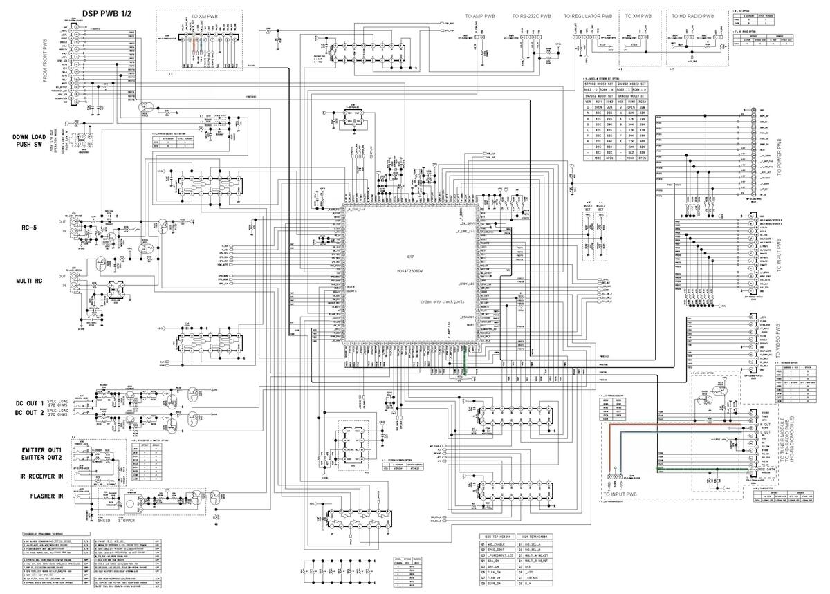


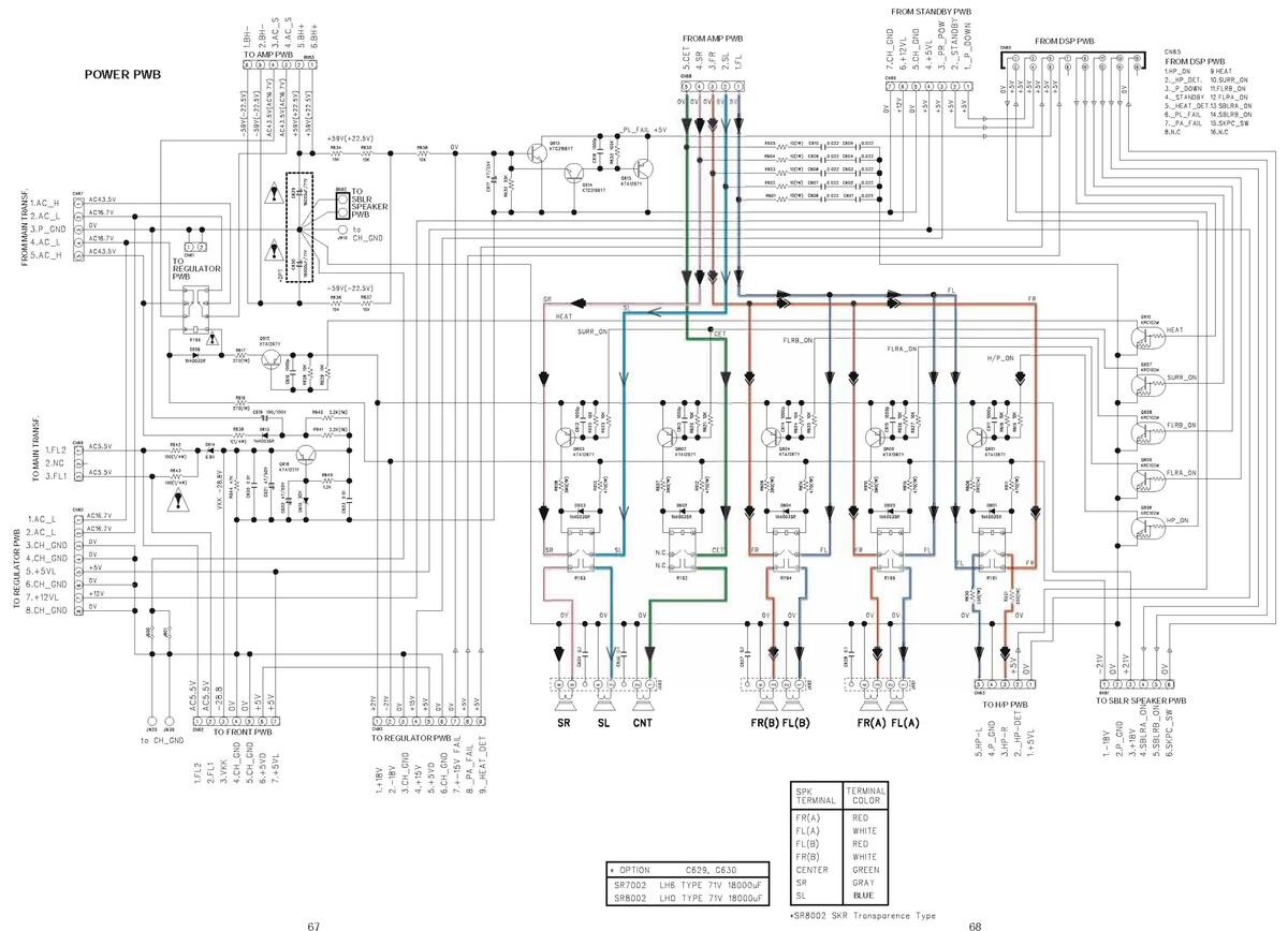


| *Option | |||||||||
|---|---|---|---|---|---|---|---|---|---|
|
SR6001
SR7001 SR8001 |
| N Ver.
|/SR7002 N/K/F |/SR8002 N/K V |
Ver.
'er. |
SR6001,
SR7002 |
/SR7001/SR8001
/SR8002 U Ver. |
U Ver. | ||||
| Ref. | Value | Use | Ref. | Value | Use | ||||
| C915 | 6800uF/35V | Х | C915 | 6800uF/35V | х | ||||
| C919 | 4700uF/35V | ٥ | C919 | 4700uF/35V | 0 | ||||
| C920 | 220uF/35V | 0 | C920 | 220uF/35V | x | ||||
11. PARTS LOCATION

鉛フリー半田 半田付けには、鉛フリー半田 (Sn-Ag-Cu) を使用してください。 Lead-free Solder

鉛フリー半田 半田付けには、鉛フリー半田 (Sn-Ag-Cu) を使用してください。
VIDEO PWB B

鉛フリー半田 半田付けには、鉛フリー半田 (Sn-Ag-Cu) を使用してください。
HDMI PWB A
|
IC96
IC98 |
Q101 Q102
Q103 |
IC11 |
Q104
( |
Q105
Q106 |
Q107
Q114 |
Q108
Q109 |
Q110
Q112 | Q113 |C13 |
Q111
C12 |
Q
IC36 |
302 Q303
IC38 |
IC3 | 9 | |
|---|---|---|---|---|---|---|---|---|---|---|---|---|---|
| IC90 |
IC14
IC32 IC3 |
IC15
33 IC34 |
IC31 | · | IC3 |
7 IC93
IC89 |
IC95 | ||||||
| Q301 | Q905 | Q90 | 01 | IC67 | IC65 | IC69 | Q805 Q80 | 6 Q809 Q810 | ) Q812 | ||||
| IC81 | Q902 |
IC82
IC83 |
IC70 | IC66 | IC68 | I | C71 |
Q807 Q808 Q810
Q606 Q818 ( |
6 Q817 Q801
Q819 Q803 Q |
Q811 Q802
813 Q814 |
|||
| l |
C92 Q904
IC97 |
Q903
IC |
264 |
IC
Q605 |
63 | Q604 | IC62 | || | C94 IC |
Q815
61 Q601 |
- Q603 |

鉛フリー半田 半田付けには、鉛フリー半田 (Sn-Ag-Cu) を使用してください。


鉛フリー半田 半田付けには、鉛フリー半田 (Sn-Ag-Cu) を使用してください。 Lead-free Solder When soldering, use the Lead-free Solder (Sn-Ag-Cu).
| DS |
QC11 QC
IC12 QC16 QC18 QC19 QC18 IC19 IC19 |
IC22
IC24 IC29 12 QC13 QC14 5 QC17 3 QC20 I4 QC21 Ə IC50 |
QC24 QC23
IC23 IC28 IC31 IC32 IC31 IC32 IC36 QC22 IC53 |
QC26 QC
QC2 IC QC25 IC IC IC 51 |
28 IC26
27 C25 C33 IC49 IC48 |
IC4
IC3 IC16 IC11 IC15 IC13 |
1
5 IC18 IC |
IC44
IC45 IC46 IC47 IC42 IC43 IC21 IC20 |
QC10 |
|---|---|---|---|---|---|---|---|---|---|
| DIG IN | |||||||||
| DIG OUT | |||||||||
|
M9-05-
M9-05- M9-05- M9-05- M9-05- M9-05- M9-05- M9-05- M9-05- M9-05- M9-05- M9-05- M9-05- M9-05- M9-05- M9-05- M9-05- M9-05- M9-05- M9-05- M9-05- M9-05- M9-05- M9-05- M9-05- M9-05- M9-05- M9-05- M9-05- M9-05- M9-05- M9-05- M9-05- M9-05- M9-05- M9-05- M9-05- M9-05- M9-05- M9-05- M9-05- M9-05- M9-05- M9-05- M9-05- M9-05- M9-05- M9-05- M9-05- M9-05- M9-05- M9-05- M9-05- M9-05- M9-05- M9-05- M9-05- M9-05- M9-05- M9-05- M9-05- M9-05- M9-05- M9-05- M9-05- M9-05- M9-05- M9-05- M9-05- M9-05- M9-05- M9-05- M9-05- M9-05- M9-05- M9-05- M9-05- M9-05- M9-05- M9-05- M9-05- M9-05- M9-05- M9-05- M9-05- M9-05- M9-05- M9-05- M9-05- M9-05- M9-05- M9-05- M9-05- M9-05- M9-05- M9-05- M9-05- M9-05- M9-05- M9-05- M9-05- M9-05- M9-05- M9-05- M9-05- M9-05- M9-05- M9-05- M9-05- M9-05- M9-05- M9-05- M9-05- M9-05- M9-05- M9-05- M9-05- M9-05- M9-05- M9-05- M9-05- M9-05- M9-05- M9-05- M9-05- M9-05- M9-05- M9-05- M9-05- M9-05- M9-05- M9-05- M9-05- M9-05- M9-05- M9-05- M9-05- M9-05- M9-05- M9-05- M9-05- M9-05- M9-05- M9-05- M9-05- M9-05- M9-05- M9-05- M9-05- M9-05- M9-05- M9-05- M9-05- M9-05- M9-05- M9-05- M9-05- M9-05- M9-05- M9-05- M9-05- M9-05- M9-05- M9-05- M9-05- M9-05- M9-05- M9-05- M9-05- M9-05- M9-05- M9-05- M9-05- M9-05- M9-05- M9-05- M9-05- M9-05- M9-05- M9-05- M9-05- M9-05- M9-05- M9-05- M9-05- M9-05- M9-05- M9-05- M9-05- M9-05- M9-05- M9-05- M9-05- M9-05- M9-05- M9-05- M9-05- M9-05- M9-05- M9-05- M9-05- M9-05- M9-05- M9-05- M9-05- M9-05- M9-05- M9-05- M9-05- M9-05- M9-05- M9-05- M9-05- M9-05- M9-05- M9-05- M9-05- M9-05- M9-05- M9-05- M9-05- M9-05- M9-05- M9-05- M9-05- M9-05- M9-05- M9-05- M9-05- M9-05- M9-05- M9-05- M9-05- M9-05- M9-05- M9-05- M9-05- M9-05- M9-05- M9-05- M9-05- M9-05- M9-05- M9-05- M9-05- M9-05- M9-05- M9-05- M9-05- M9-05- M9-05- M9-05- M9-05- M9-05- M9-05- M9-05- M9-05- M9-05- M9-05- M9-05- M9-05- M9-05- M9-05- M9-05- M9-05- M9-05- M9-05- M9-05- M9-05- M9-05- M9-05- M9-05- M9-05- M9-05- M9-05- M9-05- M9-05- M9-05- M9-05- M9-05- M9-05- M9-05- M9-05- M9-05- M9-05- M9-05- M9-05- M9-05- M9-05- M9-05- M9-05- M9-05- M9 |
|||||||||
| VR IR FLASH DC TRIC |
ARANTZ
88002/7002 P-07/08/11 |
||||||||
鉛フリー半田 半田付けには、鉛フリー半田 (Sn-Ag-Cu) を使用してください。


鉛フリー半田 半田付けには、鉛フリー半田 (Sn-Ag-Cu) を使用してください。
XM PWB A (/U Only)
| VIPWBA (/UUIIIy) | |||
|---|---|---|---|
| Q811 | IC51 | ICU3 | ICU1 |
| Q801 | IC61 | Q61 | 9 |
| IC62 | Q613 | - Q616 | |
| 1 |

XM PWB B (/U Only) ICU4 ICU2 ICU5 Q617 Q620 Q618
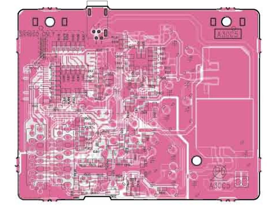
鉛フリー半田 半田付けには、鉛フリー半田 (Sn-Ag-Cu) を使用してください。 Lead-free Solder
When soldering, use the Lead-free Solder (Sn-Ag-Cu).
INPUT PWB A
| 99D A | ||||||
|---|---|---|---|---|---|---|
| IC27 | IC33 | IC35 | Q205 - Q208 | |||
| IC41 | IC36 | Q209 - Q212 | ||||
| IC21 | IC22 | IC37 | Q213 - Q216 | |||
| IC42 | IC28 | IC38 | Q217 - Q220 | |||
| IC43 | Q201 | IC34 | IC39 | Q211 - Q224 | ||
| IC44 | IC29 | Q203 | IC32 | IC40 | Q225 - Q228 | |
| IC23 - IC26 | 0229 - 0 | )244 0245 | ||||
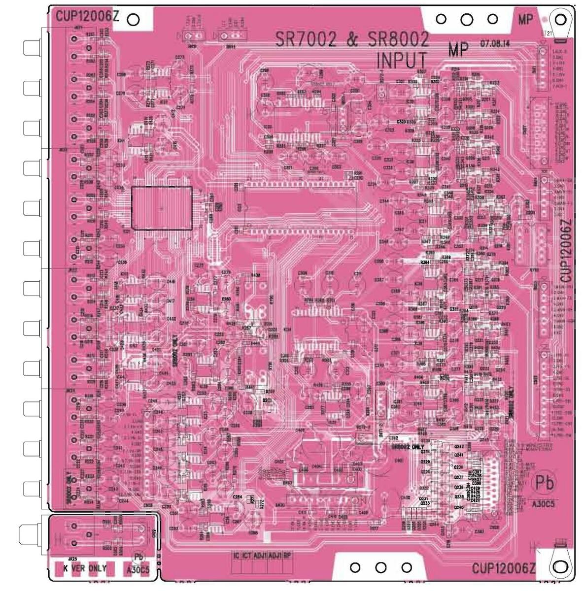
TUNER PWB A (PS7002 Only)
INPUT PWB B

HD RADIO PWB B (SR8002 /U Only) Q905 - Q909 Q901 Q902 IC92 Q904 IC93 IC91 Q903

|
鉛フリー半田
半田付けには、鉛フリー半田 (Sn-Ag-Cu) を使用してください |
|---|
|
Lead-free Solder
When soldering, use the Lead-free Solder (Sn-Ag-Cu). |
|
Q803 - Q806 Q807 (
Q810 Q8( Q802 Q801 |
Q808 Q723
09 Q707 Q715 Q709 Q713 Q717 Q711 IC71 Q703 Q705 |
Q624
Q608 Q616 Q610 Q614 Q618 Q612 Q604Q606 IC |
Q623
Q607 Q615 Q609 Q613 Q617 Q611 C61 Q603 Q605 |
Q524
Q528 Q516 Q510 Q514 Q518 Q512 Q504 Q506 IC |
Q523
Q507 Q515 Q509 Q513 Q517 Q511 C51 Q503 Q505 |
Q420
Q424 Q408 Q416 Q410 Q414 Q418 Q412 Q404 Q406 I |
Q423
Q407 Q415 Q409 Q413 Q417 Q411 C41 Q403 Q405 |
|---|---|---|---|---|---|---|---|
|
CUP12005Z
GBJ1506 + ~ ~ - |
SBR-CH
stdojn |
SR-CH
fr gray N Stdo3n |
FR-CH
£1 red N stdo3n D stdo3p |
CNT−CH
$77 GREEN N STD03N STD03P |
FL-CH
ewhite N Std03N |
SL-CH
BLUE N STD03N STD03P |
SBL-CH
white N stdo3n Stdo3p |
鉛フリー半田
半田付けには、鉛フリー半田 (Sn-Ag-Cu) を使用してください。
AMP PWB A
0.510
Lead-free Solder When soldering, use the Lead-free Solder (Sn-Ag-Cu).
AMP PWB B

鉛フリー半田 半田付けには、鉛フリー半田 (Sn-Ag-Cu) を使用してください。 Lead-free Solder
When soldering, use the Lead-free Solder (Sn-Ag-Cu).

鉛フリー半田 半田付けには、鉛フリー半田 (Sn-Ag-Cu) を使用してください。
POWER PWB B


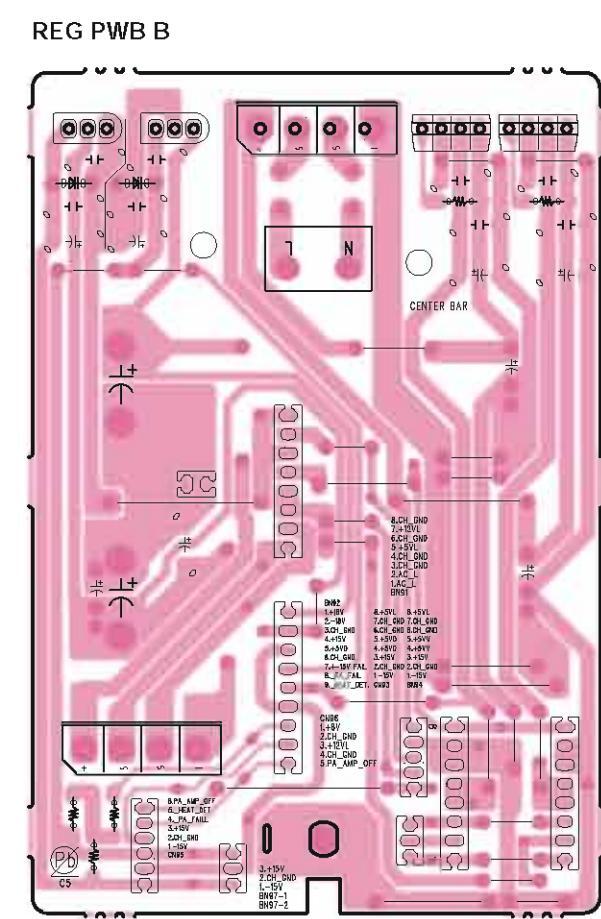
鉛フリー半田 半田付けには、鉛フリー半田 (Sn-Ag-Cu) を使用してください。

GUIDE PWB A

鉛フリー半田 半田付けには、鉛フリー半田 (Sn-Ag-Cu) を使用してください。
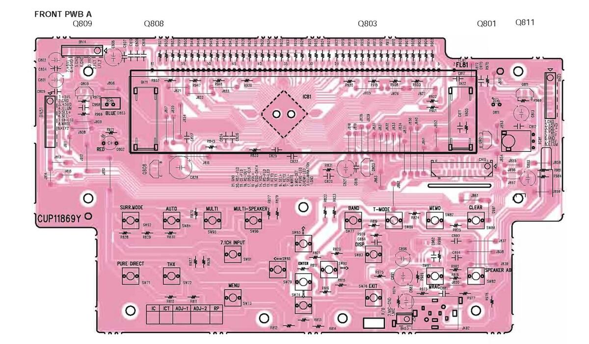
FRONT PWB B
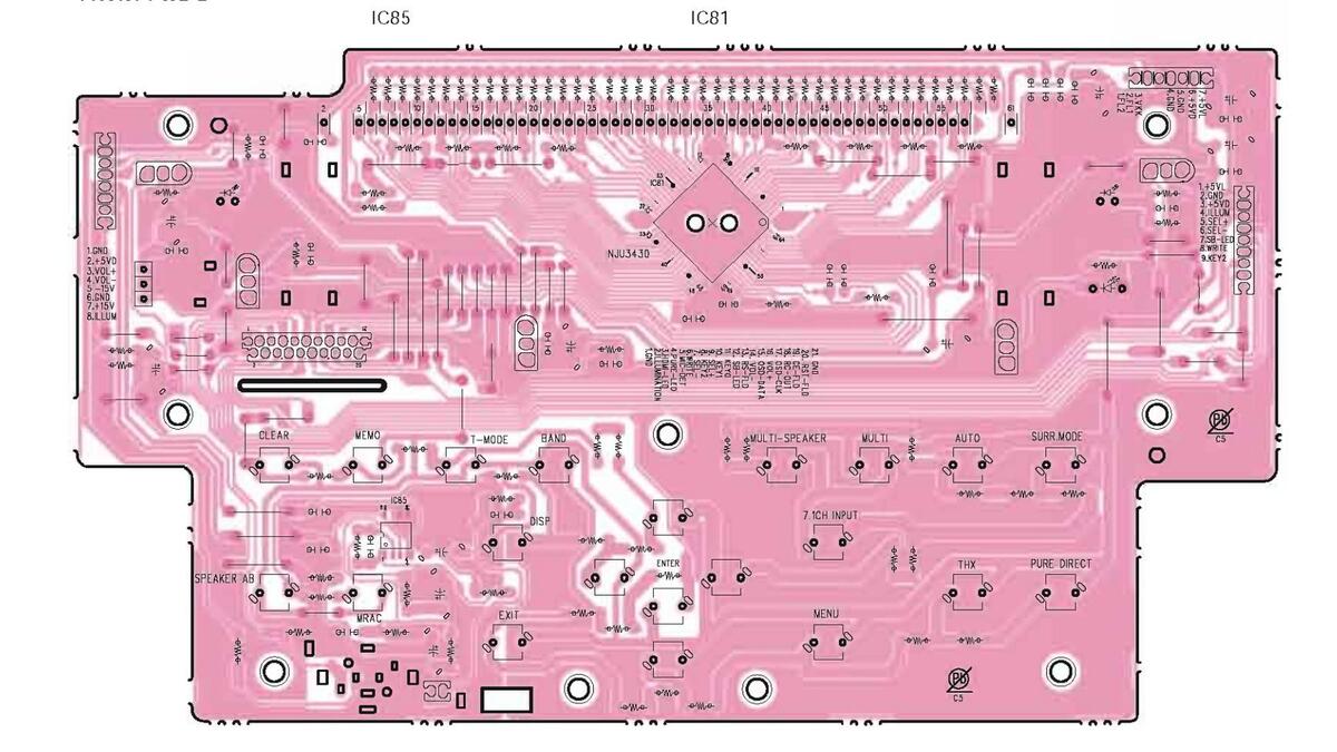
鉛フリー半田 半田付けには、鉛フリー半田 (Sn-Ag-Cu) を使用してください。


7.1CH INPUT PWB A

H/P PWB A
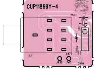

鉛フリー半田 半田付けには、鉛フリー半田 (Sn-Ag-Cu) を使用してください。


鉛フリー半田 半田付けには、鉛フリー半田 (Sn-Ag-Cu) を使用してください。 Lead-free Solder When soldering, use the Lead-free Solder (Sn-Ag-Cu).

|
P.W.B.
NAME |
POS. NO. |
VERS.
COLOR |
PART NO.
(FOR EUR) |
PART NO.
(MZ) |
PART NAME | DESCRIPTION | |
|---|---|---|---|---|---|---|---|
| 1 | FN | nsp | 00M28AW154020 | KNOB | MASTER KNOB (GOLD) | HGK1A090ZA | |
| 1 | /K1G | nsp | 00M28AW154020 | KNOB | MASTER KNOB (GOLD) | HGK1A090ZA | |
| 1 | /N1B | 00M28AW154010 | 00M28AW154010 | KNOB | MASTER KNOB (BLACK) | HGK1A090YA | |
| 1 | /N1S | 00M28AW154030 | 00M28AW154030 | KNOB | MASTER KNOB (SILVER) | HGK1A090XA | |
| 1 | /U1B | nsp | 00M28AW154010 | KNOB | MASTER KNOB (BLACK) | HGK1A090YA | |
| 2 | FN | nsp | 00M35CW248130 | PANEL | FRONT AL PANEL (GOLD) | CKM1A159MC24 | |
| 2 | /K1G | nsp | 00M35CW248110 | PANEL | FRONT AL PANEL (GOLD) | CKM1A159JC24 | |
| 2 | /N1B | 00M35CW248010 | 00M35CW248010 | PANEL | FRONT AL PANEL (BLACK) | CKM1A159MC23 | |
| 2 | /N1S | 00M35CW248210 | 00M35CW248210 | PANEL | FRONT AL PANEL (SILVER) | CKM1A159MC40 | |
| 2 | nsp | 00M35CW248020 | PANEL | ||||
| 3 | nsp | 0010135CW162130 | DOOR | DOOR AL FRONT SR7002 GOLD | |||
| 3 | 0010135000162110 | DOOR | |||||
| 3 | /N1S | 00M35CW162010 | 000035CW162010 | DOOR | DOOR AL FRONT SR7002 BLACK | CKM1A160SC/0 | |
| 3 | /IIIB | nsn | 00M35CW162010 | DOOR | CKM1A160TC23 | ||
| 4 | nsp | nsn | CONTACTOR | FABTH PLATE | CMC1A251 | ||
| 5 | FN | nsp | 00M05CW271110 | HOLDEB | DOOB HOLDEB GOLD | CKG2A046BFD4 | |
| 5 | /K1G | nsp | 00M05CW271110 | HOLDER | DOOR HOLDER GOLD | CKG2A046BFD4 | |
| 5 | /N1B | 00M05CW271050 | 00M05CW271050 | HOLDER | DOOR HOLDER BLACK | CKG2A046R4K92 | |
| 5 | /N1S | 00M05CW271210 | 00M05CW271210 | HOLDER | DOOR HOLDER SILVER | CKG2A046R6G13 | |
| 5 | /U1B | nsp | 00M05CW271050 | HOLDER | DOOR HOLDER BLACK | CKG2A046R4K92 | |
| 6 | 00M10BW112010 | 00M10BW112010 | SHAFT | SHAFT BASE | CDF1A018 | ||
| 7 | 00M10BW104010 | 00M10BW104010 | RETAINER | BRACKET BASE | CMD1A542 | ||
| 8 | FN | nsp | 00M35CW063130 | ESCUTCHEON | FRONT COVER SR7002 GOLD | CGX1A358N | |
| 8 | /K1G | nsp | 00M35CW063110 | ESCUTCHEON | COVER FRONT PS7002 GOLD | CGX1A358P | |
| 8 | /N1B | 00M35CW063010 | 00M35CW063010 | ESCUTCHEON | COVER FRONT SR7002 BLACK | CGX1A358M | |
| 8 | /N1S | 00M35CW063210 | 00M35CW063210 | ESCUTCHEON | COVER FRONT SR7002 SILVER | CGX1A358L | |
| 8 | /U1B | nsp | 00M35CW063010 | ESCUTCHEON | COVER FRONT SR7002 BLACK | CGX1A358M | |
| 9 | nsp | nsp | BRACKET | CMD2A443 | |||
| 10 | FN | nsp | 00M10BW270110 | BUITON | |||
| 10 | /K1G | 00W10BW270110 | BUITON | CBT1A95/RFZD4 | |||
| 10 | /NES | 00M10BW270010 | 0010110800270010 | BUITON | |||
| 10 |
/INTS
/IHB |
00W10BW270210 | BUTTON | OBT1A957R02013 | |||
| 11 | FN | nsp | 00M10BW270010 | BUTTON | CBT1A958BED4 | ||
| 11 | /K1G | nsp | 00M10BW270120 | BUTTON | FUNCTION BUTTON GOLD | CBT1A958BED4 | |
| 11 | /N1B | 00M10BW270020 | 00M10BW270020 | BUTTON | FUNCTION BUTTON BLACK | CBT1A958K92 | |
| 11 | /N1S | 00M10BW270220 | 00M10BW270220 | BUTTON | FUNCTION BUTTON SILVER | CBT1A958R6G13 | |
| 11 | /U1B | nsp | 00M10BW270020 | BUTTON | FUNCTION BUTTON BLACK | CBT1A958K92 | |
| 12 | 00M32CW107010 | 00M32CW107010 | SHEET | CUSHION FOOT | CHG1A360 | ||
| 13 | FN | nsp | 00M243W057010 | LEG | LEG GOLD/BLACK | CKL2A042H11 | |
| 13 | /K1G | nsp | 00M243W057010 | LEG | LEG GOLD/BLACK | CKL2A042H11 | |
| 13 | /N1B | 00M243W057010 | 00M243W057010 | LEG | LEG GOLD/BLACK | CKL2A042H11 | |
| 13 | /N1S | 00M243W057210 | 00M243W057210 | LEG | LEG FOR SILVER | CKL2A042H46 | |
| 13 | /U1B | nsp | 00M243W057010 | LEG | CKL2A042H11 | ||
| 14 | |||||||
| 10 | 000000000000000 | 00000000000000 | |||||
| 10 | |||||||
| 1/ | FN | nen | nen | ||||
| 18 | /K1G | nsp | nsp | PWB ASSY | VOLUME PWB ASSY | COP11869B | |
| 18 | /N1B | nsp | nsp | PWB ASSY | VOLUME PWB ASSY | COP11869B | |
| 18 | /N1S | nsp | nsp | PWB ASSY | VOLUME PWB ASSY | COP11869D | |
| 18 | /U1B | nsp | nsp | PWB ASSY | VOLUME PWB ASSY | COP11869C | |
| 19 | FN | nsp | 00M24AW251010 | BADGE | NEW MZ BADGE | CGB1A117 | |
| 19 | /K1G | nsp | 00M24AW251010 | BADGE | NEW MZ BADGE | CGB1A117 | |
| 19 | /N1 B | 00M24AW251010 | 00M24AW251010 | BADGE | NEW MZ BADGE | CGB1A117 | |
| 19 | /N1S | 00M24AW251020 | 00M24AW251020 | BADGE | NEW MZ BADGE SILVER | CGB1A117G | |
| 19 | /U1B | nsp | 00M24AW251010 | BADGE | NEW MZ BADGE | CGB1A117 | |
| 20 | 00M10BW355010 | 00M10BW355010 | LENS | INDICATOR POWER | CGL1A231 | ||
| 21 | nsp | nsp | CHS1A032 | ||||
| 22 | 00M35CW158010 | 00M35CW158010 | WINDOW | WINDOW FIP SR/002 | CGU1A359X | ||
| 23 | UUM4461056010 | UUM4461056010 | BUFFEK | ||||
| 24 | nsp | CHASSIS | |||||
| 24 | |||||||
| 24 | /N1S | 00M05CW105020 | 000050100020 | CHASSIS | CGW2A300R6G13 | ||
| pino | 301100011100220 | 000000000000000000000000000000000000000 | |||||
NOTE InspI PART IS LISTED FOR REFERENCE ONLY, MARANTZ WILL NOT SUPPLY THESE PARTS
| P.W.B. | VERS. | PART NO. | PART NO. | E DECODIDITION | |||
|---|---|---|---|---|---|---|---|
| NAME | POS. NO. | COLOR | (FOR EUR) | (MZ) | PARINAME | DESCRIPTION | |
| 24 | /U1B | nsp | 00M05CW105020 | CHASSIS | FRONT MOLD CHASSIS (BLACK) | CGW2A390R4K92 | |
| 25 | FN | nsp | 00M27AW270140 | BUTTON | POWER SW BUTTON (GOLD) | CBC1A146RFD4 | |
| 25 | /K1G | nsp | 00M27AW270140 | BUTTON | POWER SW BUTTON (GOLD) | CBC1A146BFD4 | |
| 25 | /N1B | 00M27AW270040 | 00M27AW270040 | BUTTON | POWER SW BUTTON (BLACK) | CBC1A146K92 | |
| 25 | /N1S | 00M27AW270240 | 00M27AW270240 | BUTTON | POWER SW BUTTON (SILVER) | CBC1A146B6G13 | |
| 26 | FN | nsn | nsn | BBACKET | POWER SW BBACKET | CMD1A493 | |
| 20 | nsp | nsp | BRACKET | ||||
| 20 | /N1B | nsp | nsp | BRACKET | |||
| 20 | /N1S | nsp | nsp | BRACKET | |||
| 20 | /NTO | 00M201U120020 | 00M201U120020 | ||||
| 21 | 00003911130030 | 00003911130030 | |||||
| 20 | nsp | nsp | DWD ACOV | ||||
| 29 | |||||||
| 30 | 0010110800355020 | 0010110800355020 | LENS | ||||
| 32 | nsp | 00IM27AW270030 | BUITON | POWER SW BUTTON TACT (BLACK) | |||
| 33 | FN | nsp | nsp | PWBASSY | SELECTOR ENCODER PWB ASSY | COP11869B | |
| 33 | /KIG | nsp | nsp | PWBASSY | SELECTOR ENCODER PWB ASSY | COP11869B | |
| 33 | /N1B | nsp | nsp | PWBASSY | SELECTOR ENCODER PWB ASSY | COP11869B | |
| 33 | /N1S | nsp | nsp | PWBASSY | SELECTOR ENCODER PWB ASSY | COP11869D | |
| 33 | /U1B | nsp | nsp | PWBASSY | SELECTOR ENCODER PWB ASSY | COP11869C | |
| 34 | FN | nsp | nsp | PWBASSY | FRONT PWB ASSY | COP11869B | |
| 34 | /K1G | nsp | nsp | PWB ASSY | FRONT PWB ASSY | COP11869B | |
| 34 | /N1B | nsp | nsp | PWB ASSY | FRONT PWB ASSY | COP11869B | |
| 34 | /N1S | nsp | nsp | PWB ASSY | FRONT PWB ASSY | COP11869D | |
| 34 | /U1B | nsp | nsp | PWB ASSY | FRONT PWB ASSY | COP11869C | |
| 35 | nsp | nsp | HEATSINK | HEAT SINK MAIN | CMY1A284Z | ||
| 36 | nsp | nsp | BRACKET | BRACKET FOR POWER AMP PWB | CMD1A490 | ||
| 37 | FN | nsp | nsp | PWB ASSY | REGULATOR PWB ASSY | COP11876D | |
| 37 | /K1G | nsp | nsp | PWB ASSY | REGULATOR PWB ASSY | COP11876D | |
| 37 | /N1B | nsp | nsp | PWB ASSY | REGULATOR PWB ASSY | COP11876D | |
| 37 | /N1S | nsp | nsp | PWB ASSY | REGULATOR PWB ASSY | COP11876D | |
| 37 | /U1B | nsp | nsp | PWB ASSY | REGULATOR PWB ASSY | COP11876E | |
| 38 | FN | nsp | nsp | PWB ASSY | AMP PWB ASSY | COP12005B | |
| 38 | /K1G | nsp | nsp | PWB ASSY | AMP PWB ASSY | COP12005B | |
| 38 | /N1B | nsp | nsp | PWB ASSY | AMP PWB ASSY | COP12005B | |
| 38 | /N1S | nsp | nsp | PWB ASSY | AMP PWB ASSY | COP12005B | |
| 38 | /U1B | nsp | nsp | PWB ASSY | AMP PWB ASSY | COP12005C | |
| 39 | nsp | nsp | BRACKET | BRACKET PWB AG-D9320 | CMD1A398 | ||
| 40 | FN | nsp | nsp | PWBASSY | POWER PWB ASSY | COP11873E | |
| 40 | /K1G | nsp | nsp | PWB ASSY | POWER PWB ASSY | COP11873D | |
| 40 | /N1B | nsp | nsp | PWBASSY | POWER PWB ASSY | COP11873D | |
| 40 | /N1S | nsp | nsp | PWBASSY | POWER PWB ASSY | COP11873D | |
| 40 | /U1B | nsp | nsp | PWBASSY | POWER PWB ASSY | COP11873E | |
| 41 | /U1B | nsp | nsp | PWBASSY | XM PWB ASSY | COP12010C | |
| 42 | FN | nsp | nsp | PWBASSY | SBLB SPEAKEB PWB ASSY | COP11874T | |
| 42 | /K1G | nsp | nsp | PWBASSY | SBLB SPEAKER PWB ASSY | COP11874F | |
| 42 | /N1B | nsp | nsp | PWBASSY | SBLB SPEAKER PWB ASSY | COP11874D | |
| 42 | /N1S | nsp | nsp | PWBASSY | SBLB SPEAKER PWB ASSY | COP11874D | |
| 42 | /LI1B | nsp | nsp | PWB ASSY | SBLB SPEAKER PM/B ASSV | COP11874E | |
| 12 | FN | nsn | nsp | PWBASSY | BS-232 PWB ASSY | COP11874T | |
| 40 | /K1G | nsn | nsp | PWBASSY | BS-232 PWB ASSY | COP11874F | |
| 10 | /N1R | nen | nen | PWR ASSV | BS-232 PWB ASSV | COP11874D | |
| 40 | /N19 | nen | nen | P\N/B ASSV | RS-232 PWR ASSV | COP1187/D | |
| 40 | /1118 | nop | nep | PMBASSY | RS-232 PM/R ASSV | COP11874E | |
| A 40 | 00MV 104002640 | ||||||
| 44 | 00W11304002040 | 001011304002040 | |||||
| 45 | nsp | nsp | DWDAGOT | COP11074F | |||
|
40
40 |
пор | пар | DIALD AGOV | ||||
| 45 | INTO | пар | |||||
| 45 | nsp | nsp | EWD ASSY | ||||
| 45 | nsp | nsp | CUACOLO | ||||
| 46 | nsp | nsp | CHASSIS | BUTTOW CHASSIS SK/002 | |||
| 4/ | nsp | nsp | HOLDER PWB CHE170 | ||||
| 48 | nsp | nsp | BRAUKET | BRACKET MAIN TRANSF. CMD1A5 | |||
| 49 | nsp | nsp | PWB ASSY | ||||
| 50 | F N | nsp | nsp | PWB ASSY | COP12006B | ||
| 50 | /KIG | nsp | nsp | PWB ASSY | |||
| 50 | /N1B | nsp | nsp | PWBASSY | COP12006B | ||
| | 50 | |/N1S | l nsp | nsp | IPWB ASSY | INPUT PWB ASSY | COP12006B | |
NOTE "nsp" PART IS LISTED FOR REFERENCE ONLY, MARANTZ WILL NOT SUPPLY THESE PARTS
| P.W.B. | POS NO | VERS. | PART NO. | PART NO. | DESCRIPTION | ||
|---|---|---|---|---|---|---|---|
| NAME | F 03. NO. | COLOR | (FOR EUR) | (MZ) | DESCRIPTION | ||
| 50 | /U1B | nsp | nsp | PWB ASSY | INPUT PWB ASSY | COP12006B | |
| 51 | 00M10BW109010 | 00M10BW109010 | SHIELD | BRACKET SHIELD | CMC1A252Z | ||
| FN | nsp | 90M-TS003200R | TRANSF. | TRANS MAIN POWER SR7002/F | CLT5W030ZJ | ||
| /K1G | nsp | 90M-TS003210R | TRANSF. | I TRANS MAIN POWER PS7002/K | CLT5W030ZH | ||
| /N1B | 90M-1S003220R | 90M-1S003220R | TRANSF. | I TRANS MAIN POWER SR7002/N | CLI5W030ZE | ||
| /N15 | 90101-1 S003220R | 90M-15003220R | TRANSF. | I TRANS MAIN POWER SR7002/N | |||
|
52
52 |
1018 | nsp | 900-15003230R | TRANSF. | |||
|
53
54 |
EN | nsp | nsp | COP11873E | |||
| 54 | /K1G | nsp | nsp | PWB ASSV | COP11873D | ||
| 54 | /N1B | nsp | nsp | PWBASSY | VIDEO PWB ASSY | COP11873D | |
| 54 | /N1S | nsp | nsp | PWBASSY | VIDEO PWB ASSY | COP11873D | |
| 54 | /U1B | nsp | nsp | PWB ASSY | VIDEO PWB ASSY | COP11873E | |
| 55 | FN | nsp | nsp | PWB ASSY | 7.1CH PREOUT PWB ASSY | COP11874T | |
| 55 | /K1G | nsp | nsp | PWB ASSY | 7.1CH PREOUT PWB ASSY | COP11874F | |
| 55 | /N1B | nsp | nsp | PWB ASSY | 7.1CH PREOUT PWB ASSY | COP11874D | |
| 55 | /N1S | nsp | nsp | PWB ASSY | 7.1CH PREOUT PWB ASSY | COP11874D | |
| 55 | /U1B | nsp | nsp | PWB ASSY | 7.1CH PREOUT PWB ASSY | COP11874E | |
| 56 | 90M-ZZ004790R | 90M-ZZ004790R | PWB ASSY | HDMI PWB ASSY | COP11982B | ||
| 57 | FN | nsp | 90M-ZZ004750R | PWB ASSY | SR7002/F DSP PWB ASSY | COP11989E | |
| 57 | /K1G | nsp | 90M-ZZ004760R | PWB ASSY | SR/002/K DSP PWB ASSY | COP11989D | |
| 5/ | /N1B | 90M-ZZ004770R | 90M-ZZ004770R | PWB ASSY | SR7002/N DSP PWB ASSY | COP11989B | |
| 5/ | /N15 | 90IVI-ZZ004770R | 90W-ZZ004770R | PWB ASSY | SR7002/N DSP PWB ASSY | COP11989B | |
|
٥/ |
1018 | nsp | 901VI-ZZ004780R | PWB ASSY | COMPONENT DWD ASSY | ||
| EN | nsp | nsp | PWD ASST | COP11869B | |||
| 50 | /K1G | nsp | nsp | PWB ASSY | COP11869B | ||
| 59 | /N1B | nsp | nsp | PWBASSY | 7 1CH INPUT PWB ASSY | COP11869B | |
| 59 | /N1S | nsp | nsp | PWB ASSY | 7.1CH INPUT PWB ASSY | COP11869D | |
| 59 | /U1B | nsp | nsp | PWB ASSY | 7.1CH INPUT PWB ASSY | COP11869C | |
| 60 | FN | nsp | 90M-AV000540R | TUNER | TUNER MODULE (JPN) | CNVMB015MA18L | |
| 60 | /N1B | 90M-AV000400R | 90M-AV000400R | TUNER | TUNER MODULE(EUR) | CNVMB114MA18L | |
| 60 | /N1S | 90M-AV000400R | 90M-AV000400R | TUNER | TUNER MODULE(EUR) | CNVMB114MA18L | |
| 60 | /U1B | nsp | 90M-AV000570R | TUNER | MODULE TUNER USA | CNVMB014MA08LS | |
| 61 | FN | nsp | nsp | PANEL | REAR PANEL SR7002 F | CKF24A306Z | |
| 61 | /K1G | nsp | nsp | PANEL | REAR PANEL PS7002 K | CKF2A334Z | |
| 61 | /N1B | nsp | nsp | PANEL | REAR PANEL SR7002 N | CKF21A306Z | |
| 61 | /N1S | nsp | nsp | PANEL | REAR PANEL SR7002 N | CKF21A306Z | |
| 10 | UIB | nsp | FANEL | REAR PANEL SR/002 0 | |||
| nsp | 9010-10002390R | FPC | CWC1C4A17B100B | ||||
| nsp | 90M-10002410H | FPC | 21 P 300MM EPC | CWC1B4A21A300A | |||
| .IW17 | nsp | 90M-YU002430B | FPC | 15P 100MM EPC | CWC3B4A15A100A | ||
| JW18 | nsp | 90M-YU003140R | FPC | 15P 150MM FPC | CWC3B4A15A150B | ||
| JW19 | nsp | 90M-YU003150R | FPC | 11P 150MM FPC | CWC3B4A11A150B | ||
| JW20 | /U1B | nsp | 90M-YU002460R | FPC | 15P 150MM FPC | CWC3C4A15B150B | |
| JW21 | FN | nsp | nsp | CORD | WIRE ASSY | CWZSR7001CN88 | |
| JW21 | /K1G | nsp | nsp | CORD | WIRE ASSY | CWZSR7001CN88 | |
| JW21 | /N1B | nsp | nsp | CORD | WIRE ASSY | CWB4F232500UU | |
| JW21 | /N1S | nsp | nsp | CORD | WIREASSY | CWB4F232500UU | |
| JW23 | nsp | nsp | CWZSR7001BN92A | ||||
| JW23(1) | 90M-FC500030K | 9010-FC500030R | |||||
|
JVV23(2)
IMO 4 |
nsp | ||||||
| nsp | 9010-10002360H | FPC | |||||
| JW26 | nsp | 90M-YU002420R | FPC | 17P 170MM FPC | CWC3B4A17A170R | ||
| JW27 | FN | nsp | 90M-YU001880B | FPC | 15P 200MM FPC | CWC1C4A15B200B | |
| JW27 | /U1B | nsp | 90M-YU001880R | FPC | 15P 200MM FPC | CWC1C4A15B200B | |
| JW28 | /N1B | nsp | 90M-YU001890R | FPC | 17P 200MM FPC | CWC1C4A17B200B | |
| JW28 | /N1S | nsp | 90M-YU001890R | FPC | 17P 200MM FPC | CWC1C4A17B200B | |
| TH1 | 90M-HP000110R | 90M-HP000110R | VARISTOR | POSISTOR ASSY | CRTSYPSX08850JD | ||
| TH2 | 90M-HP000110R | 90M-HP000110R | VARISTOR | POSISTOR ASSY | CRTSYPSX08850JD | ||
| 90M-FC500130R | 90M-FC500130R | FERRITE CORE | FERRITE CORE | CLZ9Z071Z | |||
| 90M-FC500120R | 90M-FC500120R | FERRITE CORE | FERRITE CORE | CLZ9Z070Z | |||
| 90M-FC500130R | 90M-FC500130R | FERRITE CORE | |||||
| DAOKINO | 901VI-FC500040R | 90101-FC500040R | FERRITE CORE(21.2X6.4X12.7) K5C I | ULZ9Z028Z | |||
| TAUNING |
NOTE InspI PART IS LISTED FOR REFERENCE ONLY, MARANTZ WILL NOT SUPPLY THESE PARTS
| P.W.B. | VERS. | PART NO. | PART NO. | DECODURTION | |||
|---|---|---|---|---|---|---|---|
| NAME | P05. NO. | COLOR | (FOR EUR) | (MZ) | PARINAME | DESCRIPTION | |
| FN | nsp | 00M35CW851110 | USER GUIDE | USER GUIDE SR7002 F | CQX1A1245Z | ||
| /K1G | nsp | 00M35CW851350 | USER GUIDE | USER GUIDE PS7002 K | CQX1A1246Z | ||
| /N1B | 00M35CW851310 | 00M35CW851310 | USER GUIDE | USER GUIDE SR7002 N | CQX1A1243Z | ||
| /N1S | 00M35CW851310 | 00M35CW851310 | USER GUIDE | USER GUIDE SR7002 N | CQX1A1243Z | ||
| /U1B | nsp | 00M35CW851250 | USER GUIDE | USER GUIDE SR7002 U | CQX1A1244Z | ||
| 00MZK06CW0010 | 00MZK06CW0010 | UNIT KIT | REMOTE CONTROLLER RC8001SR | CARTSR8001M | |||
| 00MZK36CW0020 | 00MZK36CW0020 | UNIT KIT | REMOTE CONTROLLER RC101 | CARTSR8002M | |||
| A 62 | FN | 90M-ZC000350R | 90M-ZC000350R | MAINS CORD | ! MAINS CORD 12A/125V | CJA2J076Z | |
| A 62 | /K1G | 90M-ZC000650R | 90M-ZC000650R | MAINS CORD | # MAINS CORD FOR K | CJA2N075Z | |
| A 62 | /N1B | 90M-ZC000320R | 90M-ZC000320R | MAINS CORD | ! MAINS CORD 2WIRE 10A/250V | CJA2B054Z | |
| A 62 | /N1S | 90M-ZC000320R | 90M-ZC000320R | MAINS CORD | ! MAINS CORD 2WIRE 10A/250V | CJA2B054Z | |
| A 62 | /U1B | 90M-ZC000310R | 90M-ZC000310R | MAINS CORD | ! MAINS CORD UL 032508/12 | CJA2A070Z | |
| 90M-ZK000670R | 90M-ZK000670R | UNIT KIT | MIC AUDYSSEY WITH FERRITE CORI | ECMICROSR8001A | |||
| NOT STAN | DARD SPAR | E PART | |||||
| FN | nsp | 00M35CW801010 | PACKING CASE | PACKING CASE SR7002 | CPG1A807Q | ||
| /K1G | nsp | 00M35CW801120 | PACKING CASE | PACKING CASE PS7002 | CPG1A807N | ||
| /N1B | nsp | 00M35CW801010 | PACKING CASE | PACKING CASE SR7002 | CPG1A807Q | ||
| /N1S | nsp | 00M35CW801010 | PACKING CASE | PACKING CASE SR7002 | CPG1A807Q | ||
| /U1B | nsp | 00M35CW801010 | PACKING CASE | PACKING CASE SR7002 | CPG1A807Q | ||
| /N1B | nsp | 00M35CW805010 | MASS CARTON | SR7002 MASTER PKG | CPG1A808W | ||
| /N1S | nsp | 00M35CW805010 | MASS CARTON | SR7002 MASTER PKG | CPG1A808W | ||
| nsp | 00M35CW809010 | CUSHION | PAD SNOW L | CPS2A744 | |||
| nsp | 00M35CW809020 | CUSHION | PAD SNOW R | CPS2A745 | |||
| 31 | FN | nsp | 00M05CW257110 | LID | TOP COVER (GOLD) | CKC1A170K118 | |
| 31 | /K1G | nsp | 00M05CW257110 | LID | TOP COVER (GOLD) | CKC1A170K118 | |
| 31 | /N1B | nsp | 00M05CW257010 | LID | TOP COVER (BLACK) | CKC1A170K117 | |
| 31 | /N1S | nsp | 00M05CW257210 | LID | TOP COVER (SILVER) | CKC1A170G14 | |
| 31 | /U1B | nsp | 00M05CW257010 | LID | TOP COVER (BLACK) | CKC1A170K117 | |
| nsp | 00M10BW067010 | CAP | COVER FOR FRONT JACK | CGR1A344 | |||
| FN | nsp | 90M-ZA000240R | ANTENNA | AM LOOP ANT | CSA1A020Z | ||
| /N1B | nsp | 90M-ZA000240R | ANTENNA | AM LOOP ANT | CSA1A020Z | ||
| /N1S | nsp | 90M-ZA000240R | ANTENNA | AM LOOP ANT | CSA1A020Z | ||
| /U1B | nsp | 90M-ZA000240R | ANTENNA | AM LOOP ANT | CSA1A020Z | ||
| FN | nsp | 90M-ZA000210R | ANTENNA | ANT FM WIRE (PIGTAIL) | CSA1A007 | ||
| /N1B | nsp | 90M-ZA000210R | ANTENNA | ANT FM WIRE (PIGTAIL) | CSA1A007 | ||
| /N1S | nsp | 90M-ZA000210R | ANTENNA | ANT FM WIRE (PIGTAIL) | CSA1A007 | ||
| /U1B | nsp | 90M-ZA000290R | ANTENNA | FM 1 POL ANT(UL) | CSA1A033Z |
13. MICROPROCESSOR AND IC DATA
IC17: HD64F2506
| pin No |
Port Na
Mode |
ame
27 |
Vcc |
I/O
Vol |
)
It I/O |
Use | STBY | Ν | lame |
V
Device |
Po
Se Act. |
ort
tup Init |
Note |
Level
Shift |
||
|---|---|---|---|---|---|---|---|---|---|---|---|---|---|---|---|---|
| 1 | PE5 | ; | P1 | +5\ | v 1/0 | 0 | 1 | RS2 | 32C_S | SW | 3.3V | RS232C Switch (Main CPU | or HDMI | |||
| 2 | PE6 | ; | P1 | +5\ | v 1/0 | 0 | I | AF | DATA | 3.3-5.0V | - | L | Analog Switch Data (TC94A | 46FG/ | ||
| 3 | PE7 | , | P1 | +5\ | v 1/0 | 0 | 1 | А | FCLK | 3.3-5.0V | - | L | Analog Switch Clock (TC94/ | 446FG/ | ||
| 4 | PDC | ) | P1 | +5\ | V 1/0 | 0 | CE | E TCA | 3.3-5.0V | Н | Analog Switch (TC94A46FG | (TC9274N) | ||||
| 5 | PD1 | P1 | +5\ | v 1/0 | 0 | 1 | R | STDA | 2 | 5.0V | L | L | Reset for DAC (CS4382) | , | ||
| 6 | PD2 | 2 | P1 | +5\ | V 1/O | 0 | | | C | S_DAG | 2 | 5.0V | L | Н | DAC CHIP SELECTION (CS | 64382) | |
| 7 | PD3 | 3 | P1 | +5\ | V 1/O | 0 | | | SW | MUT | - | 3.3-5.0V | Н | Н | SUB W SPK MUTE | , | |
| 8 | PD4 | L I | P1 | +5\ | V 1/O | 0 | 1 | CN. | TMUT | E | 3.3-5.0V | Н | Н | CENTER SPK MUTE | ||
| 9 | PD5 | 5 | P1 | +5\ | V 1/O | 0 | 1 | SB | MUTE | 3.3-5.0V | Н | Н | SRR B SPK MUTE | |||
| 10 | PD6 | 5 | P1 | +5\ | V 1/O | 0 | 1 | SL/S | RMU | ΓE | 3.3-5.0V | Н | Н | SL/SR SPK MUTE | ||
| 11 | PD7 | 7 | P1 | +5\ | v 1/0 | 0 | 1 | L/F | RMUTE | - | 3.3-5.0V | Н | Н | FRONT L/R SPK MUTE | ||
| 12 | Vss | Vss | - | 1 | , | VSS | - | - | - | GND | ||||||
| 13 | PCC | P1 | +5\ | V 1/O | 0 | 1 | KILI | FLAS | Н | 5.0V | Н | L | Kill Flasher OUT | |||
| 14 | P1Vc | c : | P1Vcc | | | | YES | 1 | , | VCC | - | - | - | +5V' | ||||
| 15 | PC1 | P1 | +5\ | V 1/O | 0 | 1 | S2F | P_DAT | A | 5.0V | - | L | 4094 Data (74HC4094 x2pc | s/CS4382) | ||
| 16 | PC2 | 2 | P1 | +5\ | V 1/O | 0 | 1 | S2 | P_CL | < | 5.0V | - | L | 4094 Clock (74HC4094 x2p | cs/CS4382) | |
| ک |
Seri2Par
Port |
ra for
Use |
/ | Na |
74
me |
1C4094 |
4 x 2pcs
V |
Ports |
(
Setup |
Vcc = 5.0V | ) | Vote | Level | |||
| Name | 0.00 | D | evice | Act. | Int | Shift | ||||||||||
| Q1 | Ο | MIC_E | NABLE | 3. | 3-5.0V | Н | L | MIC | Ena | ble f | or MRAC (Relay) | |||||
| Q2 | 0 | SPKC | CONT | 5.0V | Н | L | Spea | ker ( | C Rel | ay Control (Relay) | ||||||
| Q3 | 0 | P | PUREDI | RECT_LEI | 2 | 5.0V | L | Н | F | PURE | E DIF | RECT LED On | ||||
| Q4 | Ο | SBA | _ON | 3. | 3-5.0V | Н | L | Si | Jrr-Ba | ack S | SPK A SELECT | |||||
| Q5 | Ο | SBE | _ON | 3. | 3-5.0V | Н | L | SL | ırr-Ba | ack S | SPK B SELECT | |||||
| Q6 | 0 | FLR/ | A_ON | 3. | 3-5.0V | Н | L | S | PK A | SELECT | ||||||
| Q7 | 0 | FLR | 3_ON | 3. | 3-5.0V | Н | L | S | PK E | SELECT | ||||||
| Q8 | 0 | SUR | R_ON | 3. | 3-5.0V | Н | L | SUF | RR/C | NT SPK ON | ||||||
| Q1 | 0 | I | DIG_ | SEL_A | 3.3 | √(-5.0V) | - | L | DIGITAL IN |
1PUT
c |
SEL
SF 74' |
A FOR DIR (74HC151
VHC153) |
||||
| Q2 | 0 | I | Γ | DIG_ | SEL_B | 3.3 | √(-5.0V) | - | L | DIGITAL IN | 1PUT |
SEI
SEI |
B FOR DIR (74HC151
(/HC153) |
|||
| ŀ | + | Multi Roc | m O | Mono/Stereo SELECT | ||||||||||||
| Q3 | Ο | Μι | ulti_A M | ono/Stereo | 3. | 3-5.0V | Н | L | Mo | no :F | Stereo : L | |||||
| ľ | 1 | ~ | 1. | 10. | L | Multi Roc | m O | ut B | Mono/Stereo SELECT | |||||||
| Q4 | 0 | ulti_B M | ono/Stered | 3. | 3-5.0V | Н | L | Мо | no :F | Stereo : L | ||||||
| ľ | Q5 | Ο | | | | D | -s | 3.3V | Н | L | ADC | Mode | e Sel | ection 0 (CS5361) | ||||
| 1 | Q6 | Ο | TT | 5.0V | L | Н | Ana | log A | udio | (Lt/Rt) Input ATT | ||||||
| 1 | Q7 | Ο | I | _RS | FADC | 3.3V | L | Н | ADC | Res | set (CS5361) | |||||
| Q8 | 0 | | | | Τ | D | _A | 3. | 3-5.0V | - | L | DIR or _A | DC s |
el (l
to Fl |
Error Unsel) (74VHC08
RMUTE) |
|||
| L | - | ! | , |
| pin No |
Port Name
Mode7 |
Vcc |
I/O
Volt |
I/O | Use | STBY | Name |
V
Device |
Po
Se |
ort
tup |
Note |
Level
Shift |
|---|---|---|---|---|---|---|---|---|---|---|---|---|
| 17 | PC3 | P1 | +5V | 1/0 | 0 | S2P_STB | 5.0V | ACL. |
Init
H |
4094 Strobe (74HC4094 x2pcs) | ||
| 18 | PC4 | P1 | +5V | 1/O | 0 | 1 | S2P_ENABLE | 5.0V | - | L |
4094 Output Enable (Disable 4094 before
strobe.) (74HC4094 x2pcs) |
|
| 19 | PC5 | P1 | +5V | I/O | 0 | 1 | MULTIMUTEA | 3.3-5.0V | Н | Н | ||
| 20 | PC6 | P1 | +5V | I/O | 0 | I | MULTIMUTEB | 3.3-5.0V | Н | Н | MULTI ROOM B MUTE | |
| 21 | PC7 | P1 | +5V | I/O | 0 | 0 | KILLIR | 5.0V | Н | L | Kill to IR Input Signal | |
| 22 | PB0 | P1 | +5V | I/O | 0 | I | VOL_DATA | 5.0V | - | L | Ele Volume IC Data (TC9482) | |
| 23 | PB1 | P1 | +5V | I/O | 0 | I | VOL_CLK | 5.0V | - | L | Ele Volume IC Clock (TC9482) | |
| 24 | DDD | D1 | . 51/ | ИO | I | _TU_SD | 5.0V | L | Н | Tuner Tuned (Tuner Pack) | ||
| 24 | PDZ | PI | +50 | 10 | 0 | I | _TU_RST | 5.0V | L | Н | HD Radio CPU Reset | |
| 25 | 002 | D1 | . 5) ( | ИO | I | I | TU_ST | 5.0V | Н | Tuner Stereo/_MONO (Tuner Pack) | ||
| 25 | РБЗ | PI | +5V | 10 | 0 | _TU_WRITE | 5.0V | L | Н | HD Radio CPU Write Mode |
| pin No | Port Name | Vcc | 1/0 | I/O | Use | STBY | Name | V |
Po
Se |
ort
tup |
Note | Level |
|---|---|---|---|---|---|---|---|---|---|---|---|---|
| ľ | wode/ | Device | Act. | Init | Sniπ | |||||||
| 20 | DD4 | D1 | 51 | ПО | TU_MUTE | 5.0V | Н | Н | Tuner MUTE (Tuner Pack) | |||
| 26 | PB4 | Ы | +50 | 1/0 | 0 | TU_MUTE | 5.0V | Н | Н | Tuner MUTE (HD Radio PCB) | ||
| 27 | DDC | D1 | 51 | ПО | _CE_TU | 5.0V | L | L | Tuner PLL CE (Tuner Pack) | |||
| PB2 | PT | +5V | 1/0 | _CE_TU | 5.0V | L | L | Tuner PLL CE (HD Radio CPU) | ||||
| 28 | PB6 | P1 | +5V | I/O | 0 | I | _HDMI_LED | 5.0V | L | Н | HDMI LED On | |
| 20 | 7 9 0 | D1 | . 5) ( | ИO | (3.3-) | Power Amp DC Failure Dectection (Open | ||||||
| 29 | PD7 | Ы | VC+ | 1/0 | 5.0V | - | Collector) | |||||
| 20 | DAO | D1 | . 51/ | ИО | 0 | TUDOUT | 5.0V | - | L | Tuner PLL Data Out (Tuner Pack) | ||
| 30 | PAU | ΡI | +50 | 10 | 0 | TUDOUT | 5.0V | - | L | Tuner PLL Data Out (HD Radio CPU) | ||
| 21 | DA 1 | D1 | 51/ | ИО | 0 | TUCLK | 5.0V | - | L | Tuner PLL Clock (Tuner Pack) | ||
| 31 | PAT | PT | +30 | 17O | U | TUCLK | 5.0V | - | L | Tuner PLL Clock (HD Radio CPU) | ||
| 2.2 | D1 | 51/ | ИО | TUDIN | 5.0V | - | L | Tuner PLL Data In (Tuner Pack) | ||||
| 32 | FAZ | FI | +30 | 17O | I | TUDIN | 5.0V | - | L | Tuner PLL Data In (HD Radio CPU) | ||
| 22 | D1 | . 51/ | ИО | RDS_DIN | 5.0V | - | L | Tuner RDS Data In (Tuner Pack) | ||||
| 33 | PAS | PT | +50 | 170 | I | RDS_DIN | 5.0V | - | L | Tuner RDS Data In (HD Radio CPU) | ||
| 34 | PA4 | P1 | +5V | I/O | 0 | I | _RSTFL | 5.0V | L | L | Front FL Driver Reset (NJU3430) | |
| 35 | PA5 | P1 | +5V | I/O | О | Ι | _CEFL |
(3.3-)
5.0V |
L | L | Front FL Driver Chip Select (NJU3430) | |
| 36 | PA6 | P1 | +5V | I/O | 0 | 1 | VOL_STB | 5.0V | Н | L | Ele Volume IC Strobe (TC9482) | |
| 37 | PA7 | P1 | +5V | 1/0 | 0 | 1 | CLK_SW_0 | 3.3 | - | L | _DIR/HDMI Audio Clock Select, L:DIR, H: | |
| (-5.0)V | ||||||||||||
| 38 | PH7 | P1 | +5V | I/O | Ο | 1 | CLK SW 1 | 3.3 | - | L | HDMI MCLK ON, L:ON, H:OF | |
| (-5.0)V | | | |||||||||||
| 39 | PH6 | P1 | +5V | I/O | 0 | 1 | CLK_SW_2 | 3.3-5.0V | - | L | MCLK Select, L:DIR_MCLK, H: | |
| 40 | PH5 | P1 | +5V | 1/0 | 0 | ILLUMINATION ON OFF | 5.0V | Н | ||||
| 41 | PH4 | P1 | +5V | 1/0 |
0
0 |
HEAT | 3.3-5.0V | Н | Power Amp+B AC | Select | |||
| 112) (1 | (3.3-) | |||||||||||
| 42 | PH3 | P1 | +5V | I/O | I | _HEAT_DET | 5.0V | Н | - | Power Amp Heatsink Temp Detect | ||
| 43 | PH2 | P1 | +5V | I/O | 0 | Ι | _STANDBY |
(3.3-)
5.0V |
L | L | Standby Power | |
| 44 | PH1 | P1 | +5V | I/O | Ι | I | _HP_DET | 5.0V | L | Н | HP Jack Detect | |
| 45 | PH0 | P1 | +5V | I/O | 0 | Ι | HP_ON | 3.3-5.0V | Н | L | HEAD PHONE ON |
Ĺ
| Seri2Pa | ra for \ | /ideo | 74HC40 | )94 x 3 | 3pcs | (Vcc = 5.0V) | ||||
|---|---|---|---|---|---|---|---|---|---|---|
| Port | Heo | STRV | Namo | V | PortS | Setup | Noto | Level | ||
| Name | Use | SIDI | Name | Device | Act. | Int | Note | Shift | ||
| Q1 | 0 | MCP_MUTE | 5.0V | Multi Component MUTE | ||||||
| Q2 | 0 | SE_VIDEO03 | 5.0V | CVBS Input Select 3 (VCR/DVD/TV/AUX) (NJM2595) | ||||||
| Q3 | 0 | Ι | SE_VIDEO02 | 5.0V | CVBS Input Select 2 (VCR/DVD/TV/AUX) (NJM2595) | |||||
| Q4 | 0 | Ι | SE_VIDEO01 | 5.0V | CVBS Input Select 1 (VCR/DVD/TV/AUX) (NJM2595) | |||||
| Q5 | 0 | OSD_CON05 | 5.0V | |||||||
| Q6 | 0 | SE_VIDEO06 | 5.0V | CVBS Multi Monitor Select (Through/OSD) (NJM2244) | ||||||
| Q7 | 0 | Ι | SE_VIDEO05 | 5.0V | CVBS Multi Monitor Select (Through/OSD) (NJM2244) | |||||
| Q8 | 0 | Ι | SE_VIDEO04 | 5.0V | CVBS Input Select 4 (VCR/DVD/TV/AUX) (NJM2595) | |||||
| Q1 | 0 | I | OSD_CON01 | 5.0V | CVBS & Y/C Monitor Select (Through/Converted) (NJM2244) | |||||
| Q2 | 0 | OSD_CON02 | 5.0V | OSD Sync Input Select (MJM2535/NJM2285) | ||||||
| Q3 | 0 | OSD_CON03 | 5.0V | VIDEO DEC Input Select (MJM2285) | ||||||
| Q4 | 0 | Ι | MCP_SEL4 | 5.0V | Multi Component SEL4 | |||||
| Q5 | 0 | Ι | SEL_V02 | 5.0V | CVBS & Y/C Input Select 2 (VCR/DVD/TV/AUX) (NJM2595) | |||||
| Q6 | 0 | SEL_V01 | 5.0V | CVBS & Y/C Input Select 1 (VCR/DVD/TV/AUX) (NJM2595) | ||||||
| Q7 | 0 | SEL_V03 | 5.0V | CVBS & Y/C Input Select 3 (VCR/DVD/TV/AUX) (NJM2595) | ||||||
| Q8 | 0 | SEL_V04 | 5.0V | CVBS & Y/C Input Select 4 (VCR/DVD/TV/AUX) (NJM2595) | ||||||
| Q1 | 0 | Ι | MCP_SEL1 | 5.0V | Multi Component SEL1 | |||||
| Q2 | 0 | Y/C_SEL | 5.0V | Y/C Monitor Select (Through/Converted) (NJM2244) | ||||||
| Q3 | 0 | CVBS_SEL | 5.0V | CVBS Monitor Select (Through/Converted) (NJM2244) | ||||||
| Q4 | 0 | OSD_SEL | 5.0V | SYNC SCAN Select | ||||||
| Q5 | 0 | RST_DEC | 5.0V | VIDEO DEC Reset | ||||||
| Q6 | 0 | Ι | RST_ENC | 5.0V | VIDEO ENC Reset | |||||
| Q7 | Ο | MCP_SEL2 | 5.0V | Multi Component SEL2 | ||||||
| Q8 | 0 | Ι | MCP_SEL3 | 5.0V | Multi Component SEL3 | |||||
| pin No |
Port Name
Mode7 |
Vcc |
1/O
Volt |
1/0 | Use | STBY | Name |
V
Device |
Po
Se Act. |
ort
tup Init |
Note |
Level
Shift |
|---|---|---|---|---|---|---|---|---|---|---|---|---|
| 46 | PJ7 | P1 | +5V | I/O | SO | Ο | OSDDATA | 5.0V | - | L |
Front FL, Video (OSD), 4094 Data
(NJM3430/LC74781/74HC4094 x3pcs) |
|
| 47 | PJ6 | P1 | +5V | I/O | 0 | I | DC_OUT1 | 5.0V | L | Н | DC Triger 1 | |
| 48 | PJ5 | P1 | +5V | I/O | SC | I | OSDCLK | 5.0V | - | L |
Front FL, Video (OSD), 4094 Clock
(NJM3430/LC74781/74HC4094 x3pcs) |
|
| 49 | PJ4 | P1 | +5V | I/O | 0 | I | DC_OUT2 | 5.0V | L | Н | DC Triger 2 | |
| 50 | PJ3 | P1 | +5V | I/O | 0 | I | _CEDIR | 3.3-5.0V | L | L | DIR Chip Enable (LC89057W) | |
| 51 | PJ2 | P1 | +5V | I/O | 0 | I | _DIR_RST | 3.3-5.0V | L | L | DIR Reset (LC89057W) | |
| 52 | PJ1 | P1 | +5V | I/O | 0 | 0 | STBY_LED | 5.0V | L | Н | Standby LED On | |
| 53 | PJ0 | P1 | +5V | I/O | О | Ι | _RSFL |
(3.3-)
5.0V |
L | L |
Front FL Driver Register Selection
(NJU3430) |
|
| 54 | Vss | Vss | Ι | - | I | VSS | - | - | - | GND | ||
| 55 |
P97/AN15/
DA1 |
Avcc | +5V | I,I,O | Ι | Ι | MIC_DETECT | 5.0V | L | н | MIC Jack Detection for MRAC | |
| 56 |
P96/AN14/
DA0 |
Avcc | +5V | I,I,O | I | Ι | SPKC_SW |
(3.3-)
5.0V |
L | - | Speaker C Switch (Slide SW) | |
| 57 | P95/AN13 | Avcc | +5V | |,| | Ι | | | | DEC_INT | 3.3V | - | - | VIDEO DEC Interrupt (ADV7401) | 0 |
| 58 | P94/AN12 | Avcc | +5V | ١,١ | Ι | I | SEL- |
(3.3-)
5.0V |
L | н | Front Select Knob Encoder - | |
| 59 | P93/AN11 | Avcc | +5V | ١,١ | Ι | Ι | SEL+ |
(3.3-)
5.0V |
L | н | Front Select Knob Encoder + | |
| 60 | P92/AN10 | Avcc | +5V | ١,١ | Ι | Ι | VOL- |
(3.3-)
5.0V |
L | н | Front Vol. Knob Encoder - | |
| 61 | P91/AN9 | Avcc | +5V | ١,١ | I | I | VOL+ |
(3.3-)
5.0V |
L | Н | Front Vol. Knob Encoder + | |
| 62 | P90/AN8 | Avcc | +5V | |,| | I | Ι | _OVFL | 3.3-5.0V | - | - | ADC Overflow for Peak Indicator (CS5361) | |
| 63 | P47/AN7 | Avcc | +5V | |,| | Ι | I | TV_AUTO | 5.0V | - | - | TV Video Detect | |
| 64 | P46/AN6 | Avcc | +5V | |,| | AD | AD | MODE2 | - | - | - | CPU mode 2 | |
| 65 | P45/AN5 | Avcc | +5V | |,| | AD | AD | MODE1 | - | - | - | CPU mode 1 | |
| 66 | P44/AN4 | Avcc | +5V | |,| | AD | AD | P_LINE_FAIL | - | - | - | Emergency Protection | |
| 67 | AVss | Avss | I | - | I | AVSS | - | - | - | GND | ||
| 68 | P43/AN3 | Avcc | +5V | |,| | AD | AD | _5V_DOWN | - | - | - | Detect 5V | |
| 69 | P42/AN2 | Avcc | +5V | |,| | AD | AD | KEY2 | - | - | - | Front Button Key 2 | |
| 70 | P41/AN1 | Avcc | +5V | |,| | AD | AD | KEY1 | - | - | - | Front Button Key 1 | |
| /1 | P40/AN0 | Avcc | +5V | | |,| | AD | AD | KEYO | - | - | - | ||
| 12 | Vrer | Vrer | YES | - | - | - | +57 | |||||
| 74 | . 5V | TES |
-
2 2 5 0V |
- | - |
+5V
Serial Data for DIR /LC20057M/ |
||||||
| 74 | P50/TADZ |
P1
D1 |
+5V | 3.3-3.07 | - | - | Serial Data from DIR (LC89057W) | |||||
| 76 | P52/SCK2 | P1 | +5V | 1/0.0 | 0 | 3.3-5.0V | _ | _ | Serial Clock Out for DIB (LC89057W) | |||
| 77 | PF0/ | P1 | +5V | 1/O,I | INT | _P_DOWN | 5.0V | L | - | Power Down Detect | ||
| 78 | PF1/BUZZ | P1 | +5V | I/O,O | 0 | I | CP_SEL1 |
(3.3-)
5.0V |
Component Video Input Select 1 | |||
| 79 | PF2 | P1 | +5V | I/O | 0 | | | CP_SEL2 | (3.3-) | Component Video Input Select 2 | |||
| 80 |
PF3/
~ADTRG/ ~IRQ3 |
P1 | +5V | I/O,I,I | INT | I | RDS_CLK | 5.0V | - | - | Tuner RDS Clock (Tuner Pack) | |
| | | 1 | RDS CLK | 5.0V | - | - | Tuner RDS Clock (HD Radio CPU) | ||||||
| 01 | 54 | 5) ( | (3.3-) | Component Video Input Select 3 | ||||||||
| 81 | PF4 | P1 | +5V | 1/0 | 0 | CP_SEL3 | 5.0V | (NJM2584) 3/3 | ||||
| 82 | PF5 | P1 | +5V | I/O | 0 | I | V_CONV_SEL |
(3.3-)
5.0V |
(NJM2586) | |||
| 83 | PF6 | P1 | +5V | I/O | 0 | I | COMP_MUTE |
(3.3-)
5.0V |
Component Video Monitor Mute
(NJM2586) |
|||
| 84 | P1Vcc | P1Vcc | YES | VCC | - | - | - | +5V' | ||||
| 85 | PF7/ | P1 | +5V | 1/O,O | 0 | XPORT_SW | 3.3V | Switch of RS232C or X_PORT | 0 | |||
| 86 | Vss | Vss | - | VSS | - | - | - | GND | ||||
| 87 | TEST | NO | TEST | - | - | - | ||||||
| 88 | VCL | VCL | - | VCL | - | - | - | |||||
| 89 | 0502 | - | NC | - | - | - | ||||||
| 90 | USCI | - | V 55 | - | - | - |
| Port Name | 1/0 | ATOV | V | P | ort | Level | ||||||
|---|---|---|---|---|---|---|---|---|---|---|---|---|
| pin No | Mode7 | Vcc | Volt | 1/0 | Use | SIBY | Name | Device | Se |
tup
Unit |
Note | Shift |
| 91 | NMI | Vcc | NO | NMI | _ | H | Н | Fix : H | ||||
| 92 | MD2 | Vcc | i | YES | i | MD2 | 5.0V | H | Н | Operation : H, Boot : L | ||
| 93 | XTAL | - | YES | | | | XTAL | - | - | - | X'tal (20MHz) | |||
| 94 | Vss | Vss | Ι | NO | Ι | VSS | - | - | - | GND | ||
| 95 | EXTAL | Vcc | I | YES | I | EXTAL | - | - | - | X'tal (20MHz) | ||
| 96 | Vcc | Vcc | I | YES | Ι | VCC | - | - | - | +5V' | ||
| 97 | MD0 | Vcc | | | | YES | | | | MD0 | - | Н | Н | Fix H | ||
| 98 | MD1 | Vcc | | | | YES | MD1 | - | Н | Н | Fix H | |||
| 99 | ~STBY | Vcc | NO | _STBY | - | L | Н | Fix H | ||||
| 100 | ~RES | Vcc | YES | RES | - | L | Н | RESET | ||||
| 101 |
P20/
TIOCA3 |
P2 | +3.3V | I/O,O | О | I | CPU_NMI | 3.3V | HDMI CPU WRITE MODE (H8/36087) | |||
| 102 |
P21/
TIOCB3 |
P2 | +3.3V |
1/O,1/
O |
T_IN | I | IR_RECEIVER_IN | 5.0V | - | - | RFC | 0 |
| 103 |
P22/
TIOCC3 |
P2 | +3.3V |
1/O,1/
O |
I | I | SPIO_ENA | 3.3V | L | н |
Communication Enable from TI DSP
(DA708) |
|
| 104 | P23/ | P2 | +3.3V | 1/O,1/ | 0 | I | _TI_RST | 3.3V | L | н | Reset for TI DSP (DA708) | |
| 105 | P24/ | P2 | +3.3V | 1/0,1/ | 0 | | | | _SPIO_SCS | 3.3V | L | Н | Chip Select for TI DSP (DA708) | |
| 106 | P25/ | P2 | +3.3V | 1/0,1/ | | | XSTATE | 3.3V | Н | DIR CKST (LC89057W) | |||
| 107 | P26/ | D2 | +3 31/ |
0
1/0,1/ |
5.0V | _ | ||||||
| 107 |
TIOCA5
P27/ |
-0.0V |
0
1/0,1/ |
T_001 | 5.00 | |||||||
| 108 |
TIOCB5
P17/ |
PZ | +3.3V | 0 | 0 | M_RC_IN | 5.00 | н | Multi RC5 in Detect Signal | |||
| 109 | TIOCB2/ | P2 | +3.3V |
1/0,1/
0,1/0 |
Т | I | _P_CUR_FAIL | 3.3V | L | н | Power Amp Current Failure Detection | |
| D16/ | ||||||||||||
| 110 | TIOCA2/ | P2 | +3.3V |
1/O,1/
O,1 |
INT | INT | WAKEUP | 5.0V | - | Standby Mode Release | 0 | |
| ~IRQ1 | ||||||||||||
| 111 |
P15/
TIOCB1/ |
P2 | +3.3V | 1/0,1/ | T_IN | I | VSYNC | 5.0V | - | V-sync Det. & Change OSD (LC74781) | 0 | |
| TCLKC | 0,1/0 | |||||||||||
| 112 |
P14/
TIOCA1/ |
P2 | +3.3V | I/O,I/ | INT | REBR | 3.3V | Н | - | DIB Error (LC89057W) | ||
| ~IRQ0 | O,I | Ľ. | 0.01 | |||||||||
| P13/ | 5.0 | 1/0,1/ | 5.001 | |||||||||
| 113 | HOCD0/ | P2 | +3.3V | 0,1/0 | 0 | RC_OUT | 5.0V | - | Н | RC BUS OUT | ||
| 114 |
P12/
TIOCC0/ |
P2 | +3.3V |
1/0,1/
0,1/0 |
О | I/O | V_SDA | 3.3V | - | н |
I2C Data for VIDEO DEC/ENC (ADV7401/
ADV7320/CD0040AF) |
|
| 115 |
P11/
TIOCB0 |
P2 | +3.3V |
1/O,
1/O |
0 | Ο | V_SCL | 3.3V | - | Н | (ADV7401/ADV7320/CD0040AF) | |
| 116 | P10/ | P2 | +3.3V | 1/O, | T_IN | I | RC_IN | 5.0V | - | IR In for RC-5 | 0 | |
| 117 | Vss | Vss | VES | 22V | * | |||||||
| 118 | P2Vrc | P2Vcc | YES | VCC | _ | _ | - | +3.3V | ||||
| 119 | P37/TxD4 | P2 | +3.3V | 1/0.0 | 50 | 0 | 3.31/ | _ | н | LIABT for XM Module | ||
| 120 | P36/RxD4 | P2 | +3.3V | 1/0,1 | SI | 3.3V | - | Н | UABT for XM Module | |||
| 120 | P35/SCK1/ | 12 | 10.01 | 1/0.1/ | 0.01 | |||||||
| SCK4/ | 0.1/ | |||||||||||
| 121 | SCL0/ | P2 | +3.3V | 0,1/ | SC | CPU SCL | 3.3V | - | Н | HDMI CPU I/F (H8/36087) | ||
| ~IRQ5 | O,I | |||||||||||
| 100 | P34/RxD1/ | D 0 | 2.01 | 1/O,I, | 010 | 2.014 | ||||||
| SDA0 | PZ | +3.3V | 1/0 | SIO | CPU SDA | 3.3V | - | Н | ||||
| 123 | P33/TxD1/ | P2 | +3.3V | I/O,O, | 0 | I | CPU RST | 3.3V | L | Н | HDMI CPU Reset (H8/36087) | |
| SCL1 | · · | Ē | | | |||||||||
| 104 | P3Z/SCK0/ | D 0 | 0.007 | 1617 | | . | 2.011 | |. | |||||
| ~IRQ4 | PZ | +3.3V |
0,1/
0,1 |
HUMI_MUTE | - | THDMLMUTE (S119033) |
| pin No | Port Name | Vcc | 1/0 | I/O | Use | STBY | Name | V |
Po
Se |
ort
tup |
Note | Level |
|---|---|---|---|---|---|---|---|---|---|---|---|---|
| Node/ | Volt | Device | Act. | Init | Shift | |||||||
| 125 | P31/RxD0 | P2 | +3.3V | I/O,I | SI | I | RXD | 3.3V | - | н |
"UART for RS232C, Flash WR Pull UP
RESET : "H" |
|
| 126 | P30/TxD0 | P2 | +3.3V | I/O,O | SC | I | TXD | 3.3V | - | Н | UART for RS232C, Flash WR Pull UP | |
| 127 | P77/TxD3 | P2 | +3.3V | I/O,O | SO | I | SPIO_SIMO | 3.3V | - | Н | Serilal Data Out for TI DSP (DA708) | |
| 128 | P76/RxD3 | P2 | +3.3V | 1/O,1 | SI | I | SPIO_SOMI | 3.3V | - | L | Serial Data In from TI DSP (DA708) | |
| 129 |
P75/
TMO3/ SCK3 |
P2 | +3.3V |
1/0,1/
0,1/0 |
SC | Ι | SPIO_CLK | 3.3V | - | L | Serial Clock Out for TI DSP (DA708) | |
| 130 |
P74/
TMO2/ ~MRES |
P2 | +3.3V | I/O,O | 0 | ο | IICCLK | 3.3V | - | L | I2C Clock for E2PROM (AT24C128) | |
| 131 | P73/TMO1 | P2 | +3.3V | I/O,O | I/O | I/O | IICDATA | 3.3V | - | L | I2C Data for E2PROM (AT24C128) | |
| 132 | P72/TMO0 | P2 | +3.3V | I/O,O | 0 | I | XM_CMD | 3.3V | Н | L | DTIC mode select (XM Module) | |
| 133 |
P71/
TMRI23/ TMCI23 |
P2 | +3.3V |
1/O,
O,O |
0 | I | XM_RST | 3.3V | L | L | Reset for XM DTIC (XM Module) | |
| 134 |
P70/
TMRI01/ TMCI01 |
P2 | +3.3V |
I/O,
O,O |
0 | Ι | _XM_DAC_RST | 3.3V | L | L | DAC Reset for XM_Module (CS4392) | |
| 135 | PG4 | P1 | +5V | I/O | 0 | XM_MUTE | 5.0V | Н | Н | Mute On for XM Module | ||
| 136 | PG3 | P1 | +5V | I/O | NO | I | N.C | - | - | L | OPEN | |
| 137 | PG2 | P1 | +5V | I/O | NO | I | N.C | - | - | L | OPEN | |
| 138 |
PG1/
~IRQ7 |
P1 | +5V | I/O,I | INT | Ι | _AMUTE0 | 3.3V | L | Н | MUTE Contorol from TI DSP (DA708) | 0 |
| 139 |
PG0/
~IRQ6 |
P1 | +5V | I/O,I | INT | Ι | XM_IRQ | 3.3V | L | Н | XM error detect (XM Module) | 0 |
| 140 | PE0 | P1 | +5V | I/O | 0 | XM_ON | 5.0V | Н | L |
Control Power to XM/DT Bus (XM
Module) |
||
| 141 | PE1 | P1 | +5V | I/O | 0 | Ι | _CEEX | 5.0V | L | Н |
Serial to Parallel Expander for Video
Strobe (74HC4094 x3pcs) |
|
| 142 | PE2 | P1 | +5V | I/O | Ο | Y_OSD | 5.0V | Н | L | Y/C_OSD_IC_BYPASS (NJM2595) | ||
| 143 | PE3 | P1 | +5V | I/O | Ο | CVBS_OSD | 5.0V | Н | L | CVBS_OSD_IC_BYPASS (NJM2595) | ||
| 144 | PE4 | P1 | +5V | I/O | Ο | I | _CEOSD | 5.0V | L | Н | Video Circuit (LC74781) |
IC81 : HD64F36049HV
| Port S | Settina | |||||||
|---|---|---|---|---|---|---|---|---|
| pin | port | I/O | use | SIBY | Name | Act. | init | Note |
| 1 | PB6/AN6 | | | | | - | SW0 | - | - | to GND or Pull up selectable |
| 2 | PB7/AN7 | _ | SW1 | - | - | to GND or Pull un selectable | ||
| 3 | Avcc | AVcc | _ | - | _ | _ | A/D ref V = +5V | |
| 4 | X2 | 0 | - | _ | _ | _ | _ | |
| 5 | X1 | _ | _ | NC | ||||
| 6 | Vel | Vel | ||||||
| - 1 | _ | - | also uso for TTAC | |||||
| β | - 1 | _ | L | _ | to Vec | |||
| Vcc | 1 | Vee | - | - | _ | - | ||
| 10 | 0502 | - |
-
20MU-z |
- | - | |||
| 11 | 0502 | - | - | - | ||||
| 12 | - 1 | - | ΖΟΙΫΙΠΖ | - | - | |||
| 12 | - 1 | - | - | - | ||||
| 13 | IVIINI | - | - | - | ||||
| 14 | P87 | 1/0 | - | - | JIAG | - | - | |
| 15 | P86 | 1/0 | - | - | JIAG | - | - | |
| 10 | P85 | 1/0 | - | - | JIAG | - | - | |
| P37 | 1/0 | - | DEBLIG 00 | - | to virtual Connector Land | |||
| 18 | P36 | 1/0 | 0 | - | DEBUG_06 | - | to Virtual Connector Land | |
| 19 | P35 | 1/0 | 0 | - | DEBUG_05 | - | L | to Virtual Connector Land |
| 20 | P34 | I/O | 0 | - | DEBUG_04 | - | L | to Virtual Connector Land |
| 21 | P33 | I/O | 0 | - | DEBUG_03 | - | L | to Virtual Connector Land |
| 22 | P32 | I/O | 0 | - | DEBUG_02 | - | L | to Virtual Connector Land |
| 23 | P31 | I/O | 0 | - | DEBUG_01 | - | L | to Virtual Connector Land |
| 24 | P30 | I/O | 0 | - | DEBUG_00 | - | L | to Virtual Connector Land |
| 25 | P14/_IRQ0 | I/O | - | INT_RX | L | - | HDMI Rx device Int. | |
| 26 | P15/_IRQ1 | I/O | - | INT_TX1 | L | - | HDMI Tx device1 Int. | |
| 27 | P16/_IRQ2 | I/O | - | INT_TX2 | L | - | HDMI Tx device2 Int. | |
| 28 | P17/_IRQ3 | I/O | - | _SCDT | L | - | SCDT | |
| 29 | P57/SCL | I/O | SCL | - | CPU_SCL | L | Н | Commnunication to Main CPU |
| 30 | P56/SDA | I/O | SDA | - | CPU_SDA | - | Н | Commnunication to Main CPU |
| 31 | P55/_WKP5 | I/O | 0 | - | SW_AUDIO_EN | AUDIO Enable/Through switch | ||
| 32 | P54/_WKP4 | I/O | 0 | - | WP_CH4 | L | Н | Write Enable E2PROM4 |
| 33 | P53/_WKP3 | I/O | 0 | - | _RST_SW | L | Н | HDMI Switch device Reset |
| 34 | P52/_WKP2 | I/O | 0 | - | _RST_RX | L | Н | HDMI Rx device Reset |
| 35 | P51/_WKP1 | I/O | 0 | - | _RST_TX2 | L | Н | HDMI Tx device2 Reset |
| 36 | P50/_WKP0 | I/O | 0 | - | _RST_TX1 | L | Н | HDMI Tx device1 Reset |
| 37 | P24 | I/O | 0 | - | HDMI_SCL | L | Н | I2C Line for HDMI Control |
| 38 | P23 | I/O | 1/0 | - | HDMI_SDA | L | Н | I2C Line for HDMI Control |
| 39 | P22/TXD | I/O | TXD | - | AUX_TxD | L | Н | RS232C TxD for Host I/F |
| 40 | P21/RXD | I/O | RXD | - | AUX_RxD | L | Н | RS232C RxD for Host I/F |
| 41 | P20/SCK3 | I/O | 0 | - | - | L | N.C | |
| 42 | P60/FTIOA0 | I/O | 0 | - | SW_VIDE01 | L | Н | Select Video Decoder |
| 43 | P61/FTIOB0 | I/O | 0 | - | SW_VIDE02 | L | Н | Select I/P Converter |
| 44 | P62/FTIOC0 | I/O | FTIOC | - | CEC_IN | L | - | CEC input |
| 45 | P63/FTIOD0 | I/O | FTIOD | - | CEC_OUT | L | Н | CEC output |
| 46 | P64/FTIOA1 | I/O | 0 | - | SW 5V1 | Н | L | +5V output for SINK1 |
| 47 | P65/FTIOB1 | I/O | 0 | - | SW 5V2 | Н | L | +5V output for SINK2 |
| 48 | P66/FTIOC1 | I/O | 0 | - | HPD CH123 | Н | L | HPD Output for SRC1.2.3 |
| 49 | P67/FTIOD1 | 1/0 | 0 | _ | HPD CH4 | Н | L | HPD Output for SRC4 |
| 50 | Vss | Vss | _ | - | - | - | To GND | |
| 51 | P80/FTCI | 1/0 | - | _ | - | - | To GND | |
| 52 | P81/FTIOA | 1/O | _ | _ | - | - | To GND | |
| 53 | P82/FTIOR | _ | _ | - | To GND | |||
| 54 | To GND | |||||||
| 54 | 1/0 | _ | _ | - | To GND | |||
| 56 | 1/0 | (reserved) | _ | N C. | ||||
| 57 | P11/D\\/M | 1/0 | _ | (reserved) | N C | |||
| 57 | D12 | 1/0 | 0 | _ | (reserved) | N C | ||
| 1 20 | | 1 1 4 | 10 | (reserved) | - |
IC81 : HD64F36049HV
| nin | port | 1/0 | C TDV | Nomo | Port S | Setting | Nieto | |
|---|---|---|---|---|---|---|---|---|
| pin | μοιτ | 1/0 | use | SIDI | Name | Act. | init | Note |
| 59 |
P90/
SCK3_3 |
1/0 | 0 | - | DEBUG_X0 | - | L | N.C to Virtual Connector Land |
| 60 | P91/RXD_3 | I/O | 0 | - | DEBUG_X1/RxD1 | - | Н | N.C to Virtual Connector Land |
| 61 | P92/TXD_3 | 1/0 | 0 | - | DEBUG_X2/TxD1 | - | Н | N.C to Virtual Connector Land |
| 62 | P93 | 1/0 | 0 | - | DEBUG_X3 | - | L | N.C to Virtual Connector Land |
| 63 | P94 | 1/0 | 0 | - | DEBUG_X4 | - | L | N.C to Virtual Connector Land |
| 64 | P95 | 1/0 | 0 | - | DEBUG_X5 | - | L | N.C to Virtual Connector Land |
| 65 | P96 | 1/0 | 0 | - | DEBUG_X6 | - | L | N.C to Virtual Connector Land |
| 66 | P97 | 1/0 | 0 | - | DEBUG_X7 | - | L | N.C to Virtual Connector Land |
| 67 |
P70/
SCK3_2 |
I/O | I | - | INT_SW | - | Sil9185 Int pin | |
| 68 | P71/RXD_2 | I/O | RXD | - | DEBUG_RxD0 | L | Н | RS232C RxD for Debug |
| 69 | P72/TXD_2 | I/O | TXD | - | DEBUG_TxD0 | L | Н | RS232C TxD for Debug |
| 70 | P74/TMRIV | 1/0 | - | - | - | - | To GND | |
| 71 | P75/TMCIV | I/O | I | - | - | - | - | To GND |
| 72 | P76/TMOV | I/O | I | - | - | - | - | To GND |
| 73 | P77 | I/O | I | - | - | - | - | To GND |
| 74 | AVss | AVss | - | - | - | - | GND | |
| 75 | PB0/AN0 | - | I_5V_CH1 | - | - | 5V Input of SOURCE1 | ||
| 76 | PB1/AN1 | - | I_5V_CH2 | - | - | 5V Input of SOURCE2 | ||
| 77 | PB2/AN2 | - | I_5V_CH3 | - | - | 5V Input of SOURCE3 | ||
| 78 | PB3/AN3 | - | I_5V_CH4 | - | - | 5V Input of SOURCE4 | ||
| 79 | PB4/AN4 | I | - | I_HPD_CH1 | - | - | HPD Input of SINK1 | |
| 80 | PB5/AN5 | - | I HPD CH2 | - | - | HDP Input of SINK2 |
IC91 : R5F21246SNFP [HD RADIO CPU] (SR8002 /U only)
| PIN | DODTNUME | ATEN | Port S | Setup | ||||
|---|---|---|---|---|---|---|---|---|
| No | PORTNAME | 1/0 | USE | SIRA | NAME | Act. | Init | Note |
| 1 | NC | NC | - | - | NC | - | - | |
| 2 | P35/SCL/SSCK | 1/0 | 0 | _ | RDS CLK | - | Н | Interface to Main CPU (80pin / RDS CLK) |
| 3 | P33/SSI | 1/0 | Ī | _ | Nollse | _ | ||
| 4 | P34/SDA/SCS | 1/0 | 0 | _ | Nollse | _ | ||
| 5 | MODE | _ | MODE | Interface to Main CPU (25nin / Write mode) | ||||
| 6 | 1/0 | _ | Nollse | |||||
| Nollse | ||||||||
| 8 | RESET | RESET | Interface to Main CPU (24pin / Reset) | |||||
| a | XOUT | |||||||
| 10 | 74/100X | 1001 | ||||||
| 11 | _ | 16MHz Y'tal | ||||||
| 12 | - | |||||||
| 12 | - | Nolleo | - | +54 | ||||
| 13 | - | - | ||||||
| 14 | 1/0 | - | - | |||||
| 15 | PZ5/TRDIUBT | - | No Use | - | ||||
| 10 | 1/0 | - | No Use | - | ||||
| 1/ | PZ3/TRDIOD0 | 1/0 | - | No Use | - | |||
| 18 | PZZ/TRDIOCO | 1/0 | - | No Use | - | |||
| 19 | P21/TRDIOB0 | 1/0 | - | No Use | - | |||
| 20 | P20/TRDIOA0 | 1/0 | - | No Use | - | L | ||
| 21 | P17/TRAIO/INT1 | 1/0 | - | CE | L | L | Interface to Main CPU (27pin / CE) | |
| 22 | P16/CLK0 | 1/0 | 0 | - | No Use | - | L | Reserve |
| 23 | P15/RXD0 | 1/0 | - | HDRM-TX | - | Н | HD Radio Module TX | |
| 24 | P14/TXD0 | 1/0 | 0 | - | HDRM-RX | - | Н | HD Radio Module RX |
| 25 | P13/KI3/AN11 | _ | HDRM- | Н | HD Radio Module Reset | |||
| "0 | Ŭ | RESET | ||||||
| 26 | NC | NC | - | - | NC | - | ||
| 27 | P45/INT0 | 1/O | 0 | - | No Use | - | L | Reserve |
| 28 | P66/INT2/TXD1 | 1/O | 0 | - | DI | - | L | Interface to Main CPU (32pin / DI) |
| 29 | P67/INT3/RXD1 | 1/O | I | - | DO | - | L | Interface to Main CPU (33pin / DO) |
| 30 | P12/KI2/AN10 | I/O | 0 | - | Test Port | - | Н | For software development |
| 31 | P11/KI1 | I/O | 0 | - | Test Port | - | Н | For software development |
| 32 | P10/KI0/AN8 | I/O | 0 | - | Test Port | - | Н | For software development |
| 33 | P31/TRBO | I/O | 0 | - | Test Port | - | Н | For software development |
| 34 | P30/TRAO | I/O | 0 | - | Test Port | - | Н | For software development |
| 35 | P65/CLK1 | 1/0 | | | | - | CLK | - | L | Interface to Main CPU (31pin / CLK) |
| 36 | P64 | 1/0 | | | | - | No Use | - | L | |
| 37 | P63 | 1/0 | 0 | - | Test Port | - | Н | For software development |
| 38 | P07/AN0 | 1/0 | 1 | - | No Use | - | L | |
| 39 | NC | NC | - | - | NC | - | - | |
| 40 | NC | NC | - | - | NC | - | - | |
| 41 | P06/AN1 | 1/0 | 1 | - | No Use | - | L | |
| 42 | P05/AN2 | 1/0 | - | No Use | - | L | ||
| 43 | P04/AN3 | 1/0 | - | No Use | - | |||
| 44 | P42/VRFF | _ | VRFF | _ | Н | +51/ | ||
| 45 | P60/TRFO | 1/0 |
i
i |
- | Notise | - | ||
| 46 | P62 | 1/0 | - | No Use | - | |||
| 47 | P61 | 1/0 | - | Notise | - | |||
| 48 | P03/AN4 | 1/0 | _ | _ | ||||
| 10 | Ρ02/ΔΝ5 | 1/0 | _ | Nolleo | _ | |||
| 50 | 1/0 | Nolleo | ||||||
| 50 | 1/0 | Nolleo | ||||||
| 52 | D27/SSO | 1/0 | Interface to Main CDLL (32nin / DDS Date) | |||||
| 1 74 | 10//000 | 1 WO | - I | - | L 11 | interface to Main OFO (SSPILE RDS Data) |

| Contro | l Inputs | "ON" Channel | ||||
|---|---|---|---|---|---|---|
| Inh bit | C* | В | А | MZ4051FK | MZ4052FK | MZ4053FK |
| L | L | L | L | 0 | 0X, 0Y | 0X, 0Y, 0Z |
| L | L | L | н | 1 | 1X, 1Y | 1X, 0Y, 0Z |
| L | L | Н | L | 2 | 2X, 2Y | 0X, 1Y, 0Z |
| L | L | Н | Н | 3 | 3X, 3Y | 1X, 1Y, 0Z |
| L | Н | L | L | 4 | — | 0X, 0Y, 1Z |
| L | Н | L | Н | 5 | 1X, 0Y, 1Z | |
| L | Н | Н | L | 6 | — | 0X, 1Y, 1Z |
| L | Н | Н | Н | 7 | 1X, 1Y, 1Z | |
| Н | Х | Х | Х | None | None | None |
X: Don't care, *: Except MZ4052FK
IC20 : TC74HC4094AP IC21 : TC74HC4094AP IC79 : TC74HC4094AP IC80 : TC74HC4094AP IC83 : TC74HC4094AP

| CV | OE | ст | CI | PARA | . OUT | SERI. | OUT |
|---|---|---|---|---|---|---|---|
| 0L | 51 | 51 | Q 1 | Qn | Qs | Q's | |
| Н | Н | L | L | Qn - 1 | Q7 | NC | |
| Η | Н | Н | Н | Qn - 1 | Q7 | NC | |
| ſ | Н | L | * | NC | NC | Q7 | NC |
| L | * | * | Ζ | Z | Q7 | NC | |
| Н | * | * | NC | NC | NC | Qs | |
| Ţ | L | * | * | Z | Z | NC | Qs |
X : DON'T CARE
NC : NO CHANGE
Z : HIGH IMPEDANCE
IC20 : TC74HC4094AP IC21 : TC74HC4094AP IC79 : TC74HC4094AP IC80 : TC74HC4094AP IC83 : TC74HC4094AP
IC20 Port Name PortSetup Use STBY Name Note Device Act. Int Q1 0 MIC ENABLE H L MIC Enable for MRAC (Relay) Q2 0 SPKC_CONT 5.0V H L Speaker C Relay Control (Relay) T Q3 0 Ι _PUREDIRECT_LED L H PURE DIRECT LED On L Surr-Back SPK A SELECT Q4 SBA_ON Н H L Surr-Back SPK A SELECT H L SPK A SELECT H L SPK A SELECT H L SPK B SELECT SBB_ON FLRA_ON Q5 Q6 0 Ι FLRB_ON Q7 SURR ON H L SURR/CNT SPK ON Q8 0
IC21
| Dent | V | PortSetun | |||||
|---|---|---|---|---|---|---|---|
| Name | Use | STBY | Name | Device Act. Int | Int | Note | |
| Q1 | 0 | Ι | DIG_SEL_A | 3.3V(-5.0V) | - | L | DIGITAL INPUT SEL-A FOR DIR (74HC151 or 74VHC153) |
| Q2 | 0 | Ι | DIG_SEL_B | 3.3V(-5.0V) | - | L | DIGITAL INPUT SEL-B FOR DIR (74HC151 or 74VHC153) |
| Q3 | 0 | Ι | Multi_A Mono/Stereo | 3.3-5.0V | Н | L | Multi Room Out A Mono/Stereo SELECT Mono :H Stereo : L |
| Q4 | 0 | Ι | Multi_B Mono/Stereo | 3.3-5.0V | Н | L | Multi Room Out B Mono/Stereo SELECT Mono :H Stereo : L |
| Q5 | 0 | DFS | 3.3V | Н | L | ADC Mode Selection 0 (CS5361) | |
| Q6 | 0 | _ATT | 5.0V | L | Н | Analog Audio (Lt/Rt) Input ATT | |
| Q7 | 0 | Ι | _RSTADC | 3.3V | L | Н | ADC Reset (CS5361) |
| Q8 | 0 | Ι | D_A | 3.3-5.0V | - | L | DIR or _ADC sel (Error Unsel) (74VHC08 to ERMUTE) |
IC80
| Port | STBV | Name | ٧ | PortS | etup | Note | |
|---|---|---|---|---|---|---|---|
| Name | Use | SIDI | name | Device | Act. | Int | NOLE |
| Q1 | 0 | MCP_MUTE | 5.0V | Н | - | Multi Component MUTE | |
| Q2 | 0 | SE_VIDEO03 | 5.0V | Н | - | CVBS Input Select 3 (VCR/DVD/TV/AUX) (NJM2595) | |
| Q3 | 0 | SE_VIDEO02 | 5.0V | Н | - | CVBS Input Select 2 (VCR/DVD/TV/AUX) (NJM2595) | |
| Q4 | 0 | SE_VIDEO01 | 5.0V | Н | - | CVBS Input Select 1 (VCR/DVD/TV/AUX) (NJM2595) | |
| Q5 | 0 | OSD_CON05 | 5.0V | Н | - | ||
| Q6 | 0 | SE_VIDEO06 | 5.0V | Н | - | CVBS Multi Monitor Select (Through/OSD) (NJM2244) | |
| Q7 | 0 | SE_VIDEO05 | 5.0V | Н | - | CVBS Multi Monitor Select (Through/OSD) (NJM2244) | |
| Q8 | 0 | Ι | SE_VIDEO04 | 5.0V | Н | - | CVBS Input Select 4 (VCR/DVD/TV/AUX) (NJM2595) |
IC79
| Port Lico ST | стру | Nome | ٧ | PortS | etup | Note | |
|---|---|---|---|---|---|---|---|
| Name | Use | SIBI | Name | Device | Act. | Int | Nole |
| Q1 | 0 | Ι | OSD_CON01 | 5.0V | Н | - | CVBS & Y/C Monitor Select (Through/Converted) (NJM2244) |
| Q2 | 0 | OSD_CON02 | 5.0V | Н | - | OSD Sync Input Select (MJM2535/NJM2285) | |
| Q3 | 0 | OSD_CON03 | 5.0V | Н | - | VIDEO DEC Input Select (MJM2285) | |
| Q4 | 0 | Ι | MCP_SEL4 | 5.0V | Н | - | Multi Component SEL4 |
| Q5 | 0 | SEL_V02 | 5.0V | Н | - | CVBS & Y/C Input Select 2 (VCR/DVD/TV/AUX) (NJM2595) | |
| Q6 | 0 | SEL_V01 | 5.0V | Н | - | CVBS & Y/C Input Select 1 (VCR/DVD/TV/AUX) (NJM2595) | |
| Q7 | 0 | Ι | SEL_V03 | 5.0V | Н | - | CVBS & Y/C Input Select 3 (VCR/DVD/TV/AUX) (NJM2595) |
| Q8 | 0 | SEL_V04 | 5.0V | Н | - | CVBS & Y/C Input Select 4 (VCR/DVD/TV/AUX) (NJM2595) | |
IC83
| 1000 | |||||||
|---|---|---|---|---|---|---|---|
| Port | STRV | Name | ٧ | PortS | etup | Nota | |
| Name | Use | ыы | Name | Device | Act. | Int | Note |
| Q1 | 0 | Ι | MCP_SEL1 | 5.0V | Н | - | Multi Component SEL1 |
| Q2 | 0 | Y/C_SEL | 5.0V | Н | - | Y/C Monitor Select (Through/Converted) (NJM2244) | |
| Q3 | 0 | CVBS_SEL | 5.0V | Н | - | CVBS Monitor Select (Through/Converted) (NJM2244) | |
| Q4 | 0 | Ι | OSD_SEL | 5.0V | Н | - | SYNC SCAN Select |
| Q5 | 0 | Ι | RST_DEC | 5.0V | Н | Н | VIDEO DEC Reset |
| Q6 | 0 | Ι | RST_ENC | 5.0V | Н | Н | VIDEO ENC Reset |
| Q7 | 0 | Ι | MCP_SEL2 | 5.0V | Н | - | Multi Component SEL2 |
| Q8 | 0 | Ι | MCP_SEL3 | 5.0V | Н | - | Multi Component SEL3 |

IC22 : TC9274CNG

IC27 : CS5361-KS

|
RST
M/S LRCK SCLK SCLK MCLK VD GND GND VL SDOUT HPF I 2 S/LJ |
1 2
2 2 3 2 4 2 6 1 7 1 8 1 9 1 10 1 11 1 12 1 |
24
23 22 22 20 19 18 17 16 15 14 13 |
FILT+
REFGND VQ AINR+ AINR- VA GND AINL- AINL+ OVFL M1 M0 |
|---|
| Pin Name | # | Pin Description |
|---|---|---|
| RST | 1 | Reset (Input) - The device enters a low power mode when low. |
| M/S | 2 | Master/Slave Mode (Input) - Selects operation as either clock master or slave. |
| LRCK | 3 | Left Right Clock ( Input/Output ) - Determines which channel, Left or Right, is currently active on the serial audio data line. |
| SCLK | 4 | Serial Clock (Input/Output) - Serial clock for the serial audio interface. |
| MCLK | 5 | Master Clock (Input) - Clock source for the delta-sigma modulator and digital filters. |
| VD | 6 | Digital Power ( Input ) - Positive power supply for the digital section. |
| GND | 7,18 | Ground (Input) - Ground reference. Must be connected to analog ground. |
| VL | 8 | Logic Power (Input) - Positive power for the digital input/output. |
| SDOUT | 9 | Serial Audio Data Output (Output) - Output for two's complement serial audio data. |
| MDIV | 10 | MCLK Divider (Input) - Enables a master clock divide by two function. |
| HPF | 11 | High-pass Filter Enable (Input) - Enables the Digital High-Pass Filter. |
| I 2 S/LJ | 12 | Serial Audio Interface Format Select ( Input ) -Selects either the left-justified or I 2 S format for the SAI. |
|
MO
M1 |
13,
14 |
Mode Selection ( Input ) - Determines the operational mode of the device. |
| OVFL | 15 | Overflow (Output, open drain) - Detects an overflow condition on both left and right channels. |
|
AINL+
AINL- |
16,
17 |
Differential Left Channel Analog Input ( Input ) - Signals are presented differentially to the delta-sigma modulators via the AINL+/- pins. |
| VA | 19 | Analog Power ( Input ) - Positive power supply for the analog section. |
|
AINR-
AINR+ |
20,
21 |
Differential Right Channel Analog Input ( Input ) -Signals are presented differentially to the delta-sigma modulators via the AINR+/- pins. |
| VQ | 22 | Quiescent Voltage (Output) - Filter connection for the internal quiescent reference voltage. |
| REF_GND | 23 | Reference Ground (Input) - Ground reference for the internal sampling circuits. |
| FILT+ | 24 | Positive Voltage Reference ( Output ) - Positive reference voltage for the internal sampling circuits. |
IC31 : TC7WH157FU
LOGIC DIAGRAM

TRUTH TABLE
| INP | OUT | PUTS | |||
|---|---|---|---|---|---|
| ST | SELECT | Υ | Ϋ́ | ||
| Н | × | × | × | L | Н |
| L | L | L | × | L | Н |
| L | L | Н | × | Н | L |
| L | Н | × | L | L | Н |
| L | Н | × | Н | Н | L |
x : Don't care
IC29 : LC89057WVF4E


LC89057W
| No. | Port name | 1/0 | Description |
|---|---|---|---|
| 1 | RXOUT | 0 | Data Output |
| 2 | RX0 | Digital data Input (TTL) | |
| 3 | RX1 | Digital data Input (Coaxial) | |
| 4 | RX2 | Digital data Input (TTL) | |
| 5 | RX3 | 1 | Digital data Input (TTL) |
| 6 | DGND | Digital GND | |
| 7 | DVDD | Digital VDD | |
| 8 | RX4 | Digital data Input (TTL) | |
| 9 | RX5/VI | | | | Digital data Input (TTL) |
| 10 | RX6/UI | Digital data Input (TTL) | |
| 11 | DVDD | Digital GND for PLL | |
| 12 | DGND | Digital VDD for PLL | |
| 13 | LPF | 0 | Loop filter for PLL |
| 14 | AVDD | Analog VDD for PLL | |
| 15 | AGND | Analog GND for PLL | |
| 16 | RMCK | 0 | System clock Output for R (256fs, 512fs, XIN, VCO) |
| 17 | RBCK | O/I | Bit clock Output for R (64fs) |
| 18 | DGND | Digital GND | |
| 19 | DVDD | Digital VDD | |
| 20 | RLRCK | O/I | LR clock Input/Output for R |
| 21 | RDATA | 0 | Serial Audio data Input |
| 22 | SBCK | 0 | Bit clock Output for S (32fs, 64fs, 128fs) |
| 23 | SLRCK | 0 | LR clock Output for S (fs/2, fs, 2fs) |
| 24 | SDIN | Serial Audio data Input | |
| 25 | DGND | Digital GND | |
| 26 | DVDD | Digital VDD | |
| 27 | XMCK | 0 | Oscillation amplifier |
| 28 | XOUT | 0 | XOUT |
| 29 | XIN | Ι | XIN or External clock Input (24.576MHz or 12.288MHz) |
| 30 | DVDD | Digital VDD | |
| 31 | DGND | Digital GND | |
| 32 | EMPHA/UO | 1/O | Emphasis Information / U data Output / Set for chip address |
| 33 | AUDIO/VO | I/O | Detected non-PCM / V flag Output / Set for chip address |
| 34 | CKST | 1/O | Clock timing Output / Switch to master or slave for demodulation |
| 35 | INT | 1/0 | Interrupt Output / Switch to Modulation or general-purpose I/O |
| 36 | RERR | 0 | Error Output (PLL lock, data error) |
| 37 | DO | 0 | IF, Read out data Output |
| 38 | DI | IF, Write data Input | |
| 39 | CE | IF, Chip enable Input | |
| 40 | CL | IF, Clock Input | |
| 41 | XMODE | System reset Input | |
| 42 | DGND | Digital GND | |
| 43 | DVDD | Digital VDD | |
| 44 | TMCK/PIO0 | 1/0 | 256fs system-clock Input for modulation / General-purpose I/O input/output |
| 45 | TBCK/PIO1 | 1/0 | 64fs bit-clock Input for modulation / General-purpose I/O input/output |
| 46 | TLRCK/PIO2 | 1/0 | Fs clock Input for modulation / General-purpose I/O input/output |
| 47 | TDATA/PIO3 | 1/0 | Serial audio data for modulation / General-purpose I/O input/output |
| | 48 | TXO/PIOEN | | O/L | [Modulation data Output / General-purpose I/O enable input |
1032 .TC74VHC167ET

| Outputs | ||||
|---|---|---|---|---|
| ST | SELECT | А | В | Υ |
| Н | Х | Х | Х | L |
| L | L | L | Х | L |
| L | L | Н | Х | Н |
| L | Н | Х | L | L |
| L | Н | Х | Н | Н |
X. Don't care
IC33 : TMS320DA708
- Second Generation Aureus™ DSP 1
- 11 Features
- DA708: 32-/64-Bit 250-MHz Floating-Point DSP
-
Upgrades to C67x+ CPU From DA6xx Family:
- 2X CPU Registers [64 General-Purpose]
- New Audio-Specific Instructions
- Compatible With the DA6xx C67x CPU
-
Enhanced Memory System
- 256K-Byte Unified Program/Data RAM
- 768K-Byte Unified Program/Data ROM
- Single-Cycle Data Access From CPU
- Large Program Cache (32K-Byte) Supports RAM, ROM, and External Memory
-
External Memory Interface (EMIF) Supports:
- 100-MHz SDRAM (16-Bit)
- Async Flash/SRAM (8- or 16-Bit)
-
Enhanced I/O System
- High-Performance Crossbar Switch
- Dedicated McASP DMA Bus
- Deterministic I/O Performance
-
dMAX Dual Data Movement Accelerator:
- Memory-to-Memory Transfers
- Memory-to-Peripheral Transfers
- Packing/Unpacking Delay Data
- Circular Addressing
- Non-Sequential Addressing for Reverb
-
Three Multichannel Audio Serial Ports
- Five Clock Zones and 16 Serial Data Pins
- Supports TDM, I2S, and Similar Formats
- DIT Only (McASP2)
- Two SPI Ports With 3-, 4-, and 5-Pin Options
- Two Inter-Integrated Circuit (I2C) Ports
- Real-Time Interrupt Counter/Watchdog
- Oscillator- and Software-Controlled PLL
- Commercial or Extended Temperature
- 144-Pin, 0.5-mm, PowerPAD™ Thin Quad Flatpack (TQFP) [RFP Suffix]
- Security Features Available

-
Applications
- A/V and DVD Receiver
- Multizone A/V Receiver
- HDD Jukebox
- Navigation Systems
- High-Speed Encode With Simultaneous Multichannel Decode
-
Software Support
- Dolby® Digital. Dolby® Digital EX. Dolby® Pro Logic® IIx, Dolby® Headphone. Dolby® Virtual Surround
- DTS® 5.1, DTS-ES™ 6.1, DTS Neo:6™, DTS 96/24™. DTS-ES 96/24™
- MPEG-2 AAC LC Decode
- THX® Select, THX® Ultra 2
- MP3 Encode. MP3 Decode
- WMA9 Encode, WMA9 Decode,
- WMA9 Pro Decode – HDCD® Decode
- ATRAC3plus® Encode, ATRAC3plus® Decode
- Audyssey MultEQ XT®, MultEQ®, PrevEQ®
- SRS® Circle Surround™ II (CS II)
- Waves' MaxxBass® Technology
- TI Effects Library
- TI DSD-to-PCM Decode
- TI Filter Library
- TI Performance Audio Framework (PA/F)
- TI DSP/BIOS™
- Chip Support Library and DSP Library
| SIGNAL NAME |
PIN
NO. |
TYPE (1) | PULL (2) | GPIO (3) | DESCRIPTION |
|---|---|---|---|---|---|
| External Me | mory Interfa | ace (EMIF) A | Address and Control | ||
| EM_A[0] | 91 | 0 | - | Ν | |
| EM_A[1] | 89 | 0 | - | N | |
| EM_A[2] | 88 | 0 | - | Ν | |
| EM_A[3] | 86 | 0 | - | Ν | |
| EM_A[4] | 84 | 0 | - | Ν | |
| EM_A[5] | 83 | 0 | - | Ν | |
| EM_A[6] | 80 | 0 | - | Ν | EMIF Address bus |
| EM_A[7] | 79 | 0 | - | Ν | |
| EM_A[8] | 76 | 0 | - | Ν | |
| EM_A[9] | 75 | 0 | - | Ν | |
| EM_A[10] | 93 | 0 | - | Ν | |
| EM_A[11] | 74 | 0 | - | Ν | |
| EM_BA[0] | 96 | 0 | - | Ν | SDRAM Bank Address and Asynchronous Memory |
| EM_BA[1] | 94 | 0 | - | Ν | Low-Order Address |
| EM_CS[0] | 97 | 0 | - | Ν | SDRAM Chip Select |
| EM_CS[2] | 100 | 0 | - | Ν | Asynchronous Memory Chip Select |
| EM_CAS | 37 | 0 | - | Ν | SDRAM Column Address Strobe |
| EM_RAS | 98 | 0 | - | Ν | SDRAM Row Address Strobe |
| EM_WE | 38 | 0 | - | Ν | SDRAM Write Enable |
| EM_CKE | 71 | 0 | - | N | SDRAM Clock Enable |
| EM_CLK | 70 | 0 | - | Ν | SDRAM Clock |
| EM_WE_DQM[0] | 39 | 0 | - | Ν | Write Enable or Byte Enable for EM_D[7:0] |
| EM_WE_DQM[1] | 67 | 0 | - | N | Write Enable or Byte Enable for EM_D[15:8] |
| EM_OE | 104 | 0 | - | N | SDRAM Output Enable |
| EM_RW | 102 | 0 | - | N | Asynchronous Memory Read/not Write |
Table 2-2. Terminal Functions
(1) TYPE column refers to pin direction in functional mode. If a pin has more than one function with different directions, the functions are I YPE column refers to pin direction in functional mode. If a pin has more than one function with different separated with a slash (/). PULL column: IPD = Internal Pulldown resistor IPU = Internal Pullup resistor If the GPIO column is 'Y', then in GPIO mode, the pin is configurable as an IO unless otherwise marked.
| SIGNAL NAME |
PIN
NO. |
TYPE (1) | PULL (2) | GPIO (3) | DESCRIPTION |
|---|---|---|---|---|---|
| Exter | nal Memory | Interface (E | MIF) Data Bus | ||
| EM_D[0] | 52 | ю | - | Ν | |
| EM_D[1] | 51 | ю | - | N | |
| EM_D[2] | 49 | ю | - | Ν | |
| EM_D[3] | 48 | ю | - | Ν | |
| EM_D[4] | 46 | ю | - | Ν | |
| EM_D[5] | 45 | ю | - | Ν | |
| EM_D[6] | 43 | ю | - | Ν | |
| EM_D[7] | 41 | ю | - | Ν | EMIE Data Rua II aver 16 Bital |
| EM_D[8] | 66 | ю | - | Ν | EMIF Data Bus [Lower to Bits] |
| EM_D[9] | 64 | ю | - | Ν | |
| EM_D[10] | 63 | ю | - | Ν | |
| EM_D[11] | 61 | ю | - | Ν | |
| EM_D[12] | 59 | ю | - | Ν | |
| EM_D[13] | 58 | ю | - | N | |
| EM_D[14] | 56 | ю | - | Ν | |
| EM_D[15] | 55 | ю | - | N |
Table 2-2. Terminal Functions (continued)
IC33 : TMS320DA708
| SIGNAL NAME |
PIN
NO. |
TYPE (1) | PULL (2) | GPIO (3) | DESCRIPTION |
|---|---|---|---|---|---|
| 1 | McASP0, | McASP1, M | cASP2, and | SPI1 Serial Ports | |
| AHCLKR0/AHCLKR1 | 143 | Ю | - | Y | McASP0 and McASP1 Receive Master Clock |
| ACLKR0 | 139 | ю | - | Y | McASP0 Receive Bit Clock |
| AFSR0 | 141 | ю | - | Y | McASP0 Receive Frame Sync (L/R Clock) |
| AHCLKX0/AHCLKX2 | 2 | ю | - | Y | McASP0 and McASP2 Transmit Master Clock |
| ACLKX0 | 142 | ю | - | Y | McASP0 Transmit Bit Clock |
| AFSX0 | 144 | ю | - | Y | McASP0 Transmit Frame Sync (L/R Clock) |
| AMUTE0 | 3 | 0 | - | Y | McASP0 MUTE Output |
| AXR0[0] | 113 | ю | - | Y | McASP0 Serial Data 0 |
| AXR0[1] | 115 | ю | - | Y | McASP0 Serial Data 1 |
| AXR0[2] | 116 | ю | - | Y | McASP0 Serial Data 2 |
| AXR0[3] | 117 | ю | - | Y | McASP0 Serial Data 3 |
| AXR0[4] | 119 | ю | - | Y | McASP0 Serial Data 4 |
| AXR0[5]/SPI1_SCS | 120 | ю | - | Y | McASP0 Serial Data 5 or SPI1 Slave Chip Select |
| AXR0[6]/SPI1_ENA | 121 | ю | - | Y | McASP0 Serial Data 6 or SPI1 Enable (Ready) |
| AXR0[7]/SPI1_CLK | 122 | ю | - | Y | McASP0 Serial Data 7 or SPI1 Serial Clock |
|
AXR0[8]/AXR1[5]/
SPI1_SOMI |
126 | Ю | - | Y |
McASP0 Serial Data 8 or McASP1 Serial Data 5 or
SPI1 Data Pin Slave Out Master In |
|
AXR0[9]/AXR1[4]/
SPI1_SIMO |
127 | Ю | - | Y |
McASP0 Serial Data 9
or
McASP1 Serial Data 4
or
SPI1 Data Pin Slave In Master Out |
| AXR0[10]/AXR1[3] | 130 | ю | - | Y | McASP0 Serial Data 10 or McASP1 Serial Data 3 |
| AXR0[11]/AXR1[2] | 131 | ю | - | Y | McASP0 Serial Data 11 or McASP1 Serial Data 2 |
| AXR0[12]/AXR1[1] | 134 | ю | - | Y | McASP0 Serial Data 12 or McASP1 Serial Data 1 |
| AXR0[13]/AXR1[0] | 135 | ю | - | Y | McASP0 Serial Data 13 or McASP1 Serial Data 0 |
| AXR0[14]/AXR2[1] | 137 | ю | - | Y | McASP0 Serial Data 14 or McASP2 Serial Data 1 |
| AXR0[15]/AXR2[0] | 138 | ю | - | Y | McASP0 Serial Data 15 or McASP2 Serial Data 0 |
| ACLKR1 | 9 | ю | - | Y | McASP1 Receive Bit Clock |
| AFSR1 | 12 | ю | - | Y | McASP1 Receive Frame Sync (L/R Clock) |
| AHCLKX1 | 5 | ю | - | Y | McASP1 Transmit Master Clock |
| ACLKX1 | 7 | ю | - | Y | McASP1 Transmit Bit Clock |
| AFSX1 | 11 | ю | - | Y | McASP1 Transmit Frame Sync (L/R Clock) |
| AMUTE1 | 4 | 0 | - | Y | McASP1 MUTE Output |
| SF | 910, 12C0, an | d I2C1 Seria | l Port Pins | ||
| SPI0_SOMI/I2C0_SDA | 111 | ю | - | Y | SPI0 Data Pin Slave Out Master In or I2C0 Serial Data |
| SPI0_SIMO | 110 | ю | - | Y | SPI0 Data Pin Slave In Master Out |
| SPI0_CLK/I2C0_SCL | 108 | ю | - | Y | SPI0 Serial Clock or I2C0 Serial Clock |
| SPI0_SCS/I2C1_SCL | 107 | ю | - | Y | SPI0 Slave Chip Select or I2C1 Serial Clock |
| SPI0_ENA/I2C1_SDA | 105 | Ю | - | Y | SPI0 Enable (Ready) or I2C1 Serial Data |
Table 2-2. Terminal Functions (continued)
IC33 : TMS320DA708
| SIGNAL NAME |
PIN
NO. |
TYPE (1) | PULL (2) | GPIO (3) | DESCRIPTION | ||||
|---|---|---|---|---|---|---|---|---|---|
| Clocks | |||||||||
| OSCIN | 23 | I | - | N | 1.2-V Oscillator Input | ||||
| OSCOUT | 24 | 0 | - | N | 1.2-V Oscillator Output | ||||
| OSCV DD | 25 | PWR | - | N | Oscillator 1.2-V V DD tap point (for filter only) | ||||
| OSCV SS | 22 | PWR | - | N | Oscillator V SS tap point (for filter only) | ||||
| CLKIN | 17 | I | - | N | Alternate clock input (3.3-V LVCMOS Input) | ||||
| PLLHV | 27 | PWR | - | N | PLL 3.3-V Supply Input (requires external filter) | ||||
| Device Reset | |||||||||
| RESET | 14 | I | - | N | Device reset pin | ||||
| · | · | Emula | tion/JTAG F | Port | |||||
| тск | 35 | I | IPU | N | Test Clock | ||||
| TMS | 19 | I | IPU | N | Test Mode Select | ||||
| TDI | 28 | I | IPU | N | Test Data In | ||||
| TDO | 29 | OZ | IPU | N | Test Data Out | ||||
| TRST | 21 | I | IPD | N | Test Reset | ||||
| EMU[0] | 32 | ю | IPU | N | Emulation Pin 0 | ||||
| EMU[1] | 34 | ю | IPU | N | Emulation Pin 1 | ||||
| Р | ower Pins | ||||||||
| Core Supply (CV DD ) | 8, 16, 20 | , 33, 44, 53, | 57, 65, 77, 8 | 5, 90, 101, 1 | 23, 128, 132 | ||||
| IO Supply (DV DD ) | 10, 31, 4 | 2, 50, 60, 68 | , 73, 81, 92, | 103, 112, 12 | 5, 136 | ||||
| Ground (V SS ) | 1, 6, 13, | 15, 18, 26, 3 | 0, 36, 40, 47 | , 54, 62, 69, | 72, 78, 82, 87, 95, 99, 106, 109, 114, 118, 124, 129, 133, 140 | ||||
Table 2-2. Terminal Functions (continued)
2.15 Device Block Diagram

Figure 2-3. DA708 DSP Block Diagram
PIN CONNECTIONS

BLOCK DIAGRAM

PIN DESCRIPTION
| PIN No. | SYMBOL | PIN NAME | FUNCTION | REMARK |
|---|---|---|---|---|
| 1 | V SS |
Negative power
supply pin |
||
| 28 | V DD | Positive power supply pin | ||
| 3 | L-OUTA | |||
| 26 | R-OUTA | |||
| 6 | L-OUTB | |||
| 22 | R-OUTB | |||
| 9 | L-OUTC | Volume circuit | ||
| 19 | R-OUTC | |||
| 4 | L-INA | |||
| 25 | R-INA | |||
| 7 | L-INB | |||
| 22 | R-INB | |||
| 10 | L-INC | (VR2) | ||
| 19 | R-INC | |||
| 5 | L-A-GNDA | |||
| 24 | R-A-GNDA | |||
| 8 | L-A-GNDB | |||
| 21 | R-A-GNDB | |||
| 11 | L-A-GNDC | |||
| 18 | R-A-GNDC | |||
| 12 | CS1 | Chin select input nin |
Up to 4 chips on the same bus can be
used by switching over chip select |
|
| 17 | CS2 | code. | ||
| 14 | СК | Clock input pin | Inputs clock for serial data transfer. | Low |
| 15 | DATA | Data input pin | Inputs control data for setting volume. |
threshold
value |
| 16 | STB | Strobe input pin | Inputs strobe for writing data. | input pin |
| 13 | GND | Digital GND pin | Digital ground pin | — |
| 27 | TEST | Test Pin | Normally connect to V DD pin. | — |
| 2 | NC | No connection |
IC34 : ES29LV320E
FUNCTION BLOCK DIAGRAM

LOGIC SYMBOL

FUNCTIONAL BLOCK DIAGRAM

PIN FUNCTION DESCRIPTION
| PIN | NAME | |||
|---|---|---|---|---|
| CLK | System Clock | Ac ive on the positive going edge to sample all inputs | ||
| cs | Chip Select | Disables or enables device opera ion by masking or enabling all nputs except CLK, CKE and L(U)DQM | ||
| СКЕ | Clock Enable |
Masks system clock to freeze operation from the next clock cycle.
CKE should be enabled at least one cycle prior new command. Disable input buffers for power down in standby. |
||
| A0 ~ A11 | Address |
Row / column address are multiplexed on the same pins.
Row address : RA0~RA11, column address : CA0~CA7 |
||
| A12, A13 | Bank Select Address |
Selects bank to be activated during row address latch time.
Selects bank for read / write during column address latch ime. |
||
| RAS | Row Address Strobe | Latches row addresses on the positive going edge of the CLK with | ||
| RAS low. | ||||
| Enables row access & precharge. | ||||
| Latches column address on the positive going edge of the CLK wi h | ||||
| CAS | Column Address Strobe | CAS low. | ||
| Enables column access. | ||||
| WE | Write Enable | Enables write operation and row precharge. | ||
| Latches data in starting from CAS, WE active. | ||||
| L(U)DQM | Data Input / Output Mask |
kes data output Hi-Z, tsнz after he clock and masks he output.
ocks data input when L(U)DQM active. |
||
| DQ0 ~ DQ15 | Data Input / Output | ata inputs / outputs are multiplexed on he same pins. | ||
| VDD/VSS | Power Supply / Ground | Power and ground for he input buffers and the core logic. | ||
| VDDQ / VSSQ | Data Output Power / Ground | Isolated power supply and ground for the output buffers to provide improved noise immunity. | ||
| NC | No Connection | This pin is recommended to be left No Connection on the device. | ||
IC32 : TC74VHC157FT
TRUTH TABLE
| ST | SELECT | А | В | OUIPUI |
| Н | Х | Х | X | L |
| L | L | L | Х | L |
| L | L | Н | Х | н |
| L | Н | Х | L | L |
| L | Н | Х | Н | Н |
PIN ASSIGNMENT
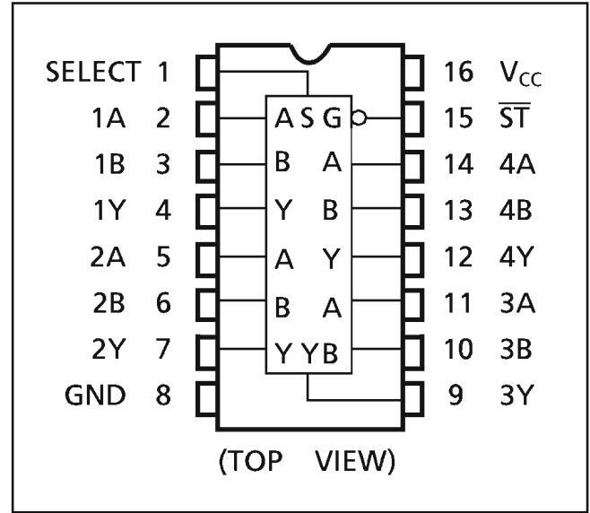
IEC LOGIC SYMBOL


 Loading...