

Page 1

Page 2

--1--
Marantz Technical Service Manual
1. FORWARD
This document defines the design and performance requirements for HYUNDAI IT
E-SERIES MODEL 26” ,32”,37”,42”,46” LCD COLOR TV
It is capable of displaying maximum 1366X768 resolution image.
The LCD TV screen comes equipped with a dedicated terminal board
which is designed to a Accommodate an image signal from a variety
of multimedia source such as DVD players,VCRs Camcoders and set-top box,CATV
2. GENERAL DESCRIPTION
2.1 Features
This digital Terrestrial receiver is suited for DVB-T standard reception of
Free digital Terrestrial program and has the following features;
<iDTV Incase>
* Full DVB-T compliant
* High quality video and CD quality sound by MPEG-2 standard
* 3000 pre-programmable station (video:2000ch,audio;1000ch)
* User friendly and well –defined On Screen Display
* Parent lock and favorite select function
* EPG(Electronic Program Guide)Function
* Full infrared remote control
* Automatic scan for added channel
* NIT scan function
* Manual and automatic scan programming
* Display signal strength meter on the screen
* Optical connector for SPDIF Output
* Output for Audio L/R
* PIG (Picture in Graphic) function
* High resolution graphic with 256 colors
* Channel delete, move, edit and add function
* Software up grade with RS232C
<Others>
* There are 7 languages OSD as English, Deutsch, Français, Nederland, Italiano,
Español, Suomi
* A choice of WIDE, ZOOM and advanced 4:3 and 14:9
AUTO size aspect ratios
* High luminance and contrast ratio, low reflection and wide viewing angle
* PIP (Picture-In-Picture)
* Auto Volume Limit
* Noise Reduction
* Sound Mode Setting(7 Equalizer : 100Hz,3200Hz,1.0KHz, 3.0KHz,10KHz)
* Picture Mode Setting
Page 3

* Full multimedia capability
* TELETEXT(252pages : only ATV)
2.3 General Specification
The LCD TV is a Color Active Matrix Liquid Crystal Display with an integral
Cold Cathode Flourscent Lamp(CCFL) backlight system.
The matrix employs a-Si Thin Film Transistor as the active element.
It is a transmissive display type which is operated in the normally black mode.
It has a 31.51 inch diagonally measured active display area with WXGA resolution.
(768 vertical by 1366 horizontal pixel array) Each pixel is divided into
Red, Green and Blue sub-pixels or dots which are arranged in vertical stripes.
Gray scale or the luminance of the sub-pixel color is determined with
a 8-bit gray scale signal for each dot, Therefore it can present a palette
of more than 16.7M(true) Colors.
It has been designed to apply the 8Bit 1 port LVDS interface.
It is intended to support LCD TV, PCTV where high brightness,
super wide viewing angle, high color gamut, high color depth and fast response
time are important
--2--
Page 4
--3--
Marantz Technical Service Manual
2.4 General Features( REFER 32”)
Page 5

3. A/V Circuit BLOCK Diagram
3.1 PC Mode
P C inputs, R, G, B , H, and V signals, are entered through D-Sub 15pin (DSUB1).
When PC is selected in MCU, the signals are entered into the SCALER, MST-6151DA
(USC01).
MST6151DA is controlled using the MCU VCT49X3R(US02) Bus line of pin
41/42/43/47/48/49/50.
PC input resolution is Fh : 31~70k and Fv: 56~85Hz, and the maximum input resolution
is 1360x768 at 60Hz.
Because MST6151DA Scaler has AD converter, data is operated RGB 24 bits.
If the resolution is above the specifications, an out of range message is displayed on the
center of the screen.
However, even if the resolution is within the specified range, if the input timing is different
from the timing indicated
on the manual, unsupported video, a message can be displayed.
The Geometry Adjust function, which is used to adjust the picture position and size,
should be carried out in the Windows desktop screen,or full cross hatch.
The component signals, 480p, 720p, and 1080i, from the set-top box with a D-Sub out
port, may be has not good image quality.
Sound L R signal of pc mode is entered pin117,118 of VCT49X3R. and sound processor
is included in VCT49X3R.
Ouput Sound signal is outputted through pin 123,124 of MST6151DA ,and then this
signal is entered audio amp YDA138E.
PC input and DVI input share a single audio jack
3.2 HDMI Mode
HDMI inputs (LVDS signal), 8bit, are entered through HDMI 19pin (CNG02). When HDMI
is selected by MCU,
the LVDS signals are entered into digital port of the SCALER MST-6151DA (USC01).
MST6151DA is controlled using the MCU Bus line of pin 41/42/43/47/48/49/50.
the maximum resolution is 1360x768 at 65Hz. If the resolution is above the specifications,
an out of range message
is displayed on the center of the screen. However, even if the resolution is within the
specified range,
if the input timing is different from the timing indicated on the manual, unsupported
video, a message can be displayed.
In hdmi mode, this model support 480p(60), 576p(50), 720p(50/60), 1080i(50/60) ,and
pc timing on the manual.
3.3 COMPONENT Mode
Component signals Y, Pb(Cb),Pr(Cr) are entered port0 of mux PI5V330SWE(UC01).
mux PI5V330SWE is controlled by mcu.
When pin 1 of mux is low, component signal is outputted, and then Component signals
--4--
Page 6

Marantz Technical Service Manual
are entered into
The SCALER, MST-6151(USC01)DA.
The Component signals are composed of 480p (50/60Hz) for SD, 576p(60Hz),720p
(50/60Hz) for HD, and 1080i (50/ 60Hz).
Component audio signal is entered audio mux TEA6422(UX01). Mux TEA6422 is
controlled by SCL,SDA line of MCU VCT49X3R.
3.4 S-Video
S-Video signals are entered as Y/ C signals, which is composed of Luminance and color
signals.
The PAL/SECAM are automatically detected by the video decoders VCT49X3R.
video decorder is included in VCT49X3R (US02).
Video signal is operated 656 format( 8bit), and YUV 8bit signal is entered scaler
video port.
S-Video input and composite video input share a single audio jack.
Therefore, while the pictures for the two inputs can be viewed at the same time, only one
of the sounds can be heard.
S-video and composite audio signal is entered audio mux TEA6422(UX01).
Mux TEA6422 is controlled by SCL,SDA line of MCU VCT49X3R.
3.5 Video
Video signal is a composite signal that combines the Luminance (Y) and color (CHROMA) .
It is entered to the scaler IC, MST-6151DA (USC01).
Video signal is operated 656 format( 8bit) as S-video , and YUV 8bit signal is entered
scaler video port.
3.6 Scart Mode
Scart mode is separated full scart mode , half scart mode.
Full scart mode support CVBS video signal and RGB signal with audio signal.
half scart mode support CVBS video signal with audio signal.
Y-C Mode Signals is not Supported.
pin 8 high will auto select the SCART input. With a voltage range of 4.5V to 7.0V a compatible set
will
select AV input in 16x9 mode. With a voltage range of 9.5v to 12.0v the set will select AV input in
4x3 mode.
pin 16 is used to select between composite or RGB input modes using the same SCART.
With a voltage of 1-3V DC (with respect to pin 18) RGBS input mode is selected.
With a voltage range of 0-0.4V composite mode is selected
3.7 IDTV Mode
--5--
Page 7
DTV Y Pb Pr signal is inputted from digital board assy .
DTV signals Y, Pb(Cb),Pr(Cr) are entered port1 of mux PI5V330SWE(UC01).
mux PI5V330SWE is controlled by mcu.
When pin 1 of mux is high, dtv signal is outputted, and then dtv signals are entered
into The SCALER, MST-6151(USC01)DA.
dtv signals are composed of 576i. dtv audio signal is entered audio mux TEA6422(UX01).
Mux TEA6422 is controlled by SCL,SDA line of MCU VCT49X3R.
3.8 Analog TV Mode
Rf signal from tuner(UX02) is generated IF. And IF signal is entered saw filter TFS96F(US01)
Output signal from saw filter is entered VCT49X3R. this signal is separated CVBS video and
audio signal in VCT49X3R.
3.9 Supported PIP/POP Table
Sub\Main
PC X X X X O O O O O
HDMI X X X X O O O O O
iDTV X X X X O O O O O
COMP X X X X O O O O O
S-VIDEO O O O O X X X X X
VIDEO O O O O X X X X X
FScart O O O O X X X X X
HScart O O O O X X X X X
ANALOG
TV
PC HDMI iDTV
O O O O X X X X X
COMP
S-VIDEO
VIDEO
FScart
HScart
ANALOG
TV
X: Not supported, O: Supported
3.10 Scaler Output
Scaler output signals is R, G, B (each 8bits) LVDS signal .
This signal sent to the logic B/D in the LCD module.
3.11 Audio part
--6--
Page 8

Marantz Technical Service Manual
Audio input port for each mode:
Input Port Remark
PC /HDMI
Scart
CVBS /S-Video
COMPONENT
RCA L/R 1EA Shared
Scart Jack L/R
RCA L /R 1EA PAL
RCA L /R 2EA
Full and half
Audio input signal for PC/HDMI,COMPONENT,S-VIDEO,SCART and CVBS modes is entered
into the
audio processor IC(VCT49X3R), The audio processor (VCT49X3R) to control volume,
and left/right balance and mono/stereo and Sound effect.
The L/ R audio signal sent by VCT49X3R is amplified in the amplifier, YDA138E
(UAU01),and sent to the speaker.
YDA138E Support 10W(based on impedance 8 ohm of output for L/R).
4
. To use Service Mode
4.1 ENTERED INTO AGING MODE
1) REMOCON CONTROL
SET UP :MENU + S. MODE + SLEEP + MUTE Then go to number 5
Then go to number 3(Aging Option) ON
SET UP REMOVE :EXIT
4.2 CHECKING MCU VERSION
1) REMOCON CONTROL
- SET UP :MENU + S. MODE + SLEEP + MUTE Then You will see MCU VERSION
- GO TO Number 6
4
. 3 FACTORY RESET
1) REMOCON CONTROL
- SET UP :MENU + S. MODE + SLEEP + MUTE Then go to number 7(FACTORY RESET)
- PRESS ENTER AND RIGHT KEY
--7--
Page 9

4. 4 IN CASE DTV
Go to DTV Source Then Press MENU and move DTV CHANNEL and move FACTORY
SET and Press ENTER
4.5. Exit Service menu
- press exit key
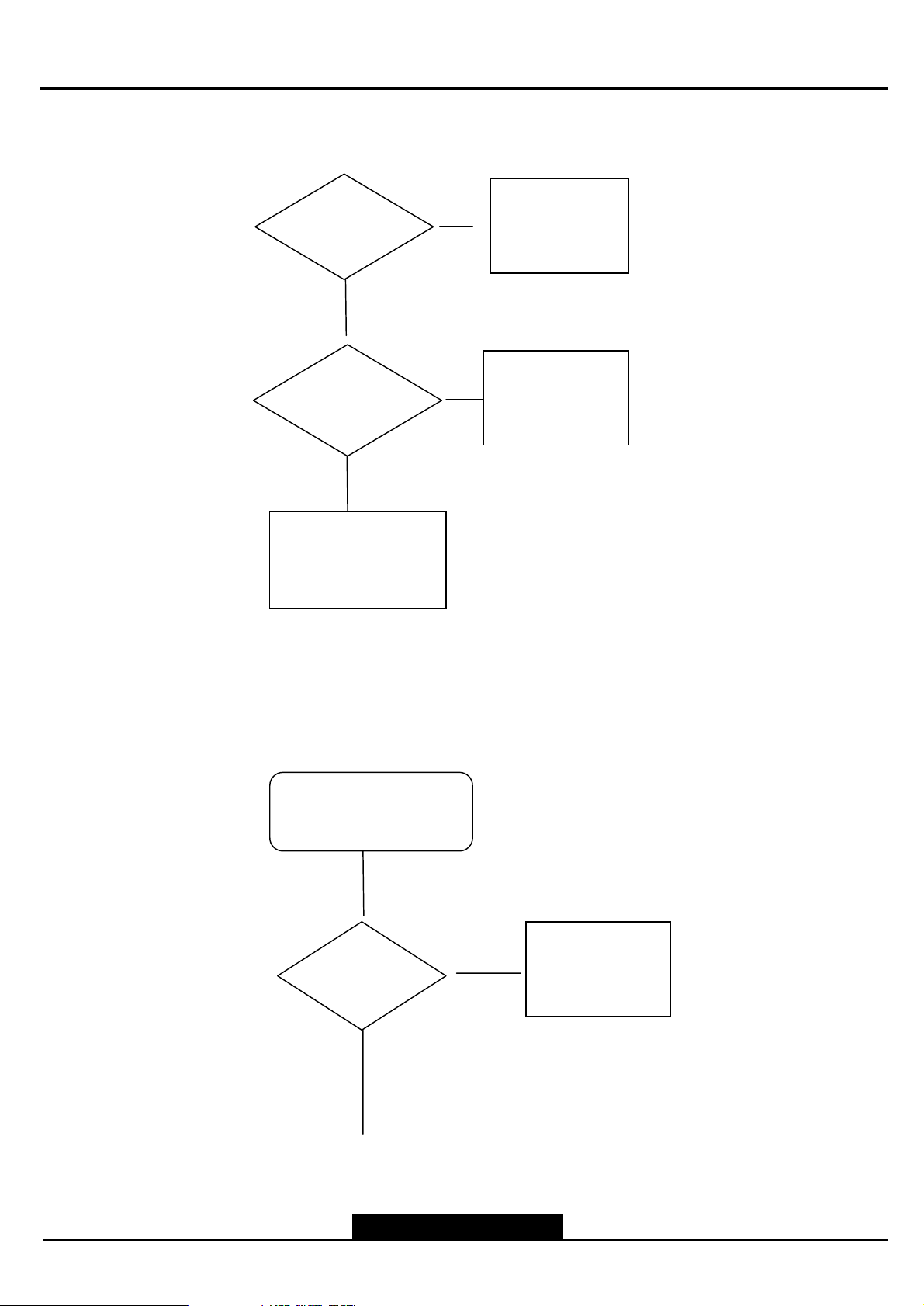
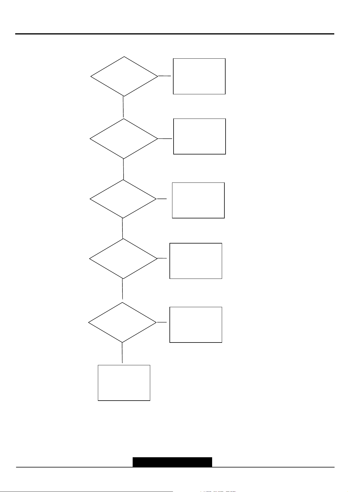
5.Trouble Shooting Guide
--8--
Page 10
Marantz Technical Service Manual
CHECK
UP09
D1.8V?
YES
NO
TROUBLE IN
UP09,USC01
CHECK UP10
MD1.8V?(IN USE
MD)
YES
CHECK END
DTV B/D CHECK
NO
TROUBLE IN
UP10
UMD01
YES
CHECK
R45,R44
(D5V D12V?)
YES
--9--
NO
TROUBLE IN
CON2
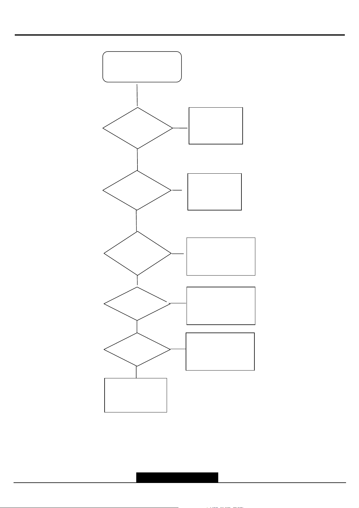
Page 11
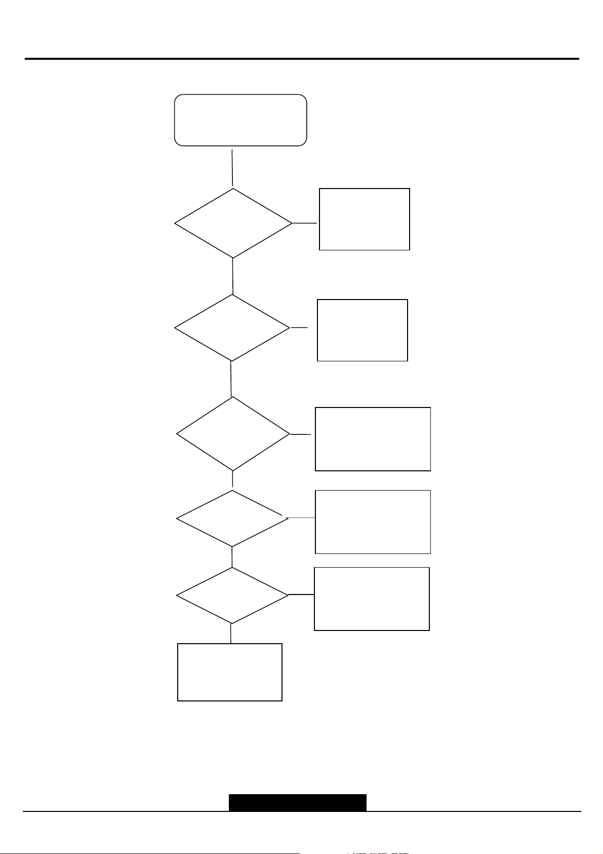
LVDS
NO RASTER
YES
NO POWER
CHECK
YES
PANEL AND
YES
CHECK PANEL
VCC OR BL_ON?
YES
NO
NO
NO
PANEL AND
LVDS CABLE
TROUBLE IN
PANEL OR
UP01
TROUBLE IN UP01
PIN2 OF CNP01
CHECK US02
OUTPUT?
YES
CHECK USC01
OUTPUT?
CHECK END
NO
TROUBLE IN US02
TROUBLE IN USC01
--10--
Page 12
Marantz Technical Service Manual
CHECK
ICDT1
(33V)?
YES
CHECK ICDT2
2.5V?,
YES
CHECK 33V
YES
NO
NO
NO
TROUBLE IN T1
U3,U4,U5
TROUBLE IN U3
TROUBLE IN
TUNER
CHECK
RX,TX
YES
CHECK T1,U3
JP5
YES
CHECK END
NO
NO
TROUBLE IN
CON02 PIN2
U3
,UG05
TROUBLE IN
TUNER
JP5
,U3,T1
--11--
Page 13
UX01
NO SOUND
YES
AUDIO SOUND
INPUT?
YES
AUDIO MUX
YES
CHECK US02
INPUT OR OUTPUT
YES
NO
NO
NO
TROUBLE IN
INPUT
TROUBLE IN
AUDIO MUX
UX01
TROUBLE IN US02
AUDIO AMP
UAU01
YES
CHECK MUTE
VOLUME
CHECK END
NO
NO
TROUBLE IN AUDIO
AMP UAU01 OR AMP
VCC
TROUBLE IN MUTE
OR VOLUME OR
SPEAKER CABLE
--12--
Page 14

Marantz Technical Service Manual
6. TV/ VIDEO System
<Digital>
6.1 Front –End(Tuner/Demodulator)
Input Frequency Range : VHF 174~230Mhz:ch5~ch12
230~470Mhz:ch71~ch99
UHF 470~860Mhz :ch21~ch69
RF Input(for aerial)connector : female IEC 169-2
Channel bandwidth German : 8Mhz/7Mhz (combine UHF/VHF)
Others : 8Mhz (UHF only)
Input Impeadance 75ohms
OFDM Spectrum 2k and 8k carrier non hierarchical
Modulation Mode 16QAM,64QAM
Guard Interval Modes 1/32,1/16,1/8,1/4 active symbol duration
FEC Modes Rate 1/2, 2/3, 3/4, 5/6, 7/8
6.2 Transport Demultiplexer
Demultiplexer According to ISO/IEC 13818-1
Max.Input Stream 60Mbps(serial)/7.5Mbps(parallel)
PID Handling Capability 32PID
SI Filtering According DVB-SI Spec.(ETS 300 468)
< Analog >
6.3 ATV STANDARD
- TV system : PAL B/G, D/K, I, L, M
- RF signal :
VHF, UHF, CABLE TV
- Sound modulation: AM/FM-Mono, FM-Stereo (A2, D/K), NICAM
- Color system : PAL, SECAM
* APPLICATION
· Receiving System : (PAL STANDARD SYSTEM )
· Channel VHF : Low BAND : E2(48.25MHz) ~ S6(140.25MHz)
High BAND : S7(147.25MHz) ~ S36(423.25MHz)
UHF BAND : S37(431.25MHz) ~ C57(863.25MHz)
· Intermediate Frequency PIF : 38.9MHz (PAL B/G, I, D/K, SECAM L)
33.9MHz (SECAM L’)
SIF : 33.4MHz (B/G), 32.9MHz( I), 32.4MHz( D/K )
40.4MHz (SECAM L’)
--13--
Page 15
· Input Impedance : UHF/VHF Terminal (75) Ω, Unbalanced
· Band Change – Over System : (PLL Control System)
· Tuning System : (Electronic Tuning System With PLL)
6.4 Power Indicator LED
The LCD TV shall make use of an LED type indicator located on the front of the LCD TV.
The LED Color shall indicate the power states as follows.
* Power ON-LED is Green
* Power Off(Stand-by)- LED is Red( <1.8 watts)
6.5 Signal Input / Output specification
Parameter Specification Unit Remarks
Speaker
Audio
Consumption
Composit Video Input 1 Vp-p
Scart Input
S- Video Input
Component
Input
PC Input
Audio Input L, R 0.5 Vrms Mono or stereo
DVI Input
Impedance 8(L) + 8(R) Ω
Output 10 W
Freq. Character 0.1 ~ 12 KHz
T.H.D < 10 %
HUM < 1 V
Output 10(L) + 10(R) W
Max 125+10% W NOTE 1 Power
ST-BY <2.0 W
Full
Half CVBS 1 Vp-p
COMP
DTV
H Frequency 31 ~ 70(TTL Level) KHz
V Frequency 56 ~ 85(TTL Level) Hz
H Frequency 31 ~ 70(TTL Level) KHz
V Frequency 60(TTL Level) Hz
RGB 0.7 Vp-p
CVBS 1 Vp-p
Y 1 Vp-p
C 0.286 Vp-p
Y 1 Vp-p
Pb 0.7 Vp-p
Pr 0.7 Vp-p
Y 1 Vp-p
Pb 0.7 Vp-p
Pr 0.7 Vp-p
RGB 0.7 Vp-p
1920 * 1080i
1280 * 720p
720 * 576p
720 * 576p
VGA ~ XGA & HDTV
(1080i, 720p, 576p)
--14--
Page 16
Marantz Technical Service Manual
VIDEO Out put Composite 1.0 Vp-p
Audio Output L,R 0.5 Vrms
Woofer out put LOUD 0.5 Vrms
Scart Output
Full CVBS 1 Vp-p
Half CVBS 1 Vp-p
NOTE 1 .Power source : AC230V 50Hz
.It is measured on full screen white pattern
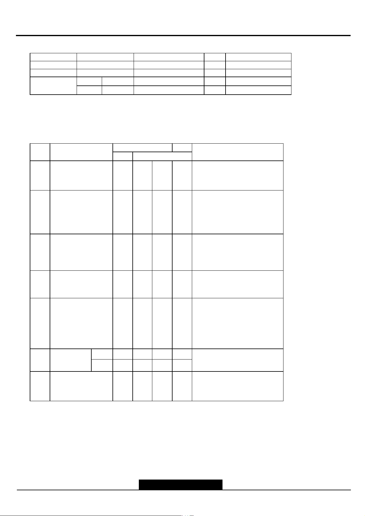
6.6 TV Input
* DEMOD. CHARACTERISTICS
NO. ITEM
1-1 Video Output Level 2.0 2.3 2.6 Vp-p * Video Signal : PAL( 87.5%),
Video Freq. Response
1 MHz 2 MHz 3 MHz 4
MHz 4.43 MHz -1.0
1-2
1-3 Luminance S/N Ratio 40 47 - dB
MIN.
-1.5
-2.5
-3.0
-4.0
SPECIFICATIONS
-0.0
-0.0
-0.0
-0.0
-1.0
+1.5
+2.0
+2.5
+3.0
+3.0
UNIT
NOTES
* Input Level : 70dBuV
SECAM ( 90%)
AM Mod. STD Color Bar
* Input Level : 70dBuV * PALl:
87.5% AM Mod. * SECAM : 90%
AM Mod. * FULL Sweepl *
dB
Reference : 0.5 MHZ
* Input Level : VHF,UHF : 70dBuV *
Setting of S/N Meter - HPF :
100KHz, - LPF : 5.0MHz * Video
Signal : 87.5% AM Mod.100%
White
Video Signal : 100% White Sig. AT.
NOISE LIMIT
1-4
SENSITIVITY
AFT ALIGNMENT
1-5
ACCURACY
Chroma
1-6
Distortion
DP -10 5 10 DEG
DG -10 5 10 %
- 43 51 dBuV
+50 0 -50 KHz
1-7 BURST LEVEL 20.0 30 36 % * Video Signal: 87.5% Mod.
S/N = 30dB
* Alignment Center : 1.9V * IF Input
Level : 90dBuV * P/S : -10dB *
Standard Color Bar : PAL(87.5%)
SECAM L’ (90%) * Center
Frequency : PAL ( 38.9 MHz)
SECAM L’ (90%)
* Input Level : 70dBuV * Video
Signal: 87.5% AM Mod. RAMP
Signal
* Input Level : 70dBuV
Standard Color
Bar Sig.
--15--
Page 17
1-8 SIF OUTPUT LEVEL 70 75
dBuV
1-9 AUDIO S/N RATIO 40 50
AUDIO DISTORTION
1-10
1-11
1-12
RESPONSE
AUDIO
FREQ.
RES-PONSE
10KHz
AUDIO OUTPUT
LEVEL
50Hz
- 4
- 0.6 3.5 %
- 3
- 1
0.3 .06 .08 Vrms
0 + 3
dB * Video Signal: 87.5% Mod.
dB
6.7 Analog R.G.B Input (PC)
6.7.1 Timing
* Input Level : 70dBuV * Video
Signal: Standard Color Bar Sig. *
CH : S20
* P/S Ratio : -10dB
* 1KHz±50KHz Dev.
Standard Color Bar Sig. * Use
CCITT FILTER
* 1KHz±50KHz Dev.
Color Bar : 87.5% Mod.
De-emphasis ON
* 50Hz ~ 10KHz *
* Standard
*
1KHz±50KHz
Dev *Standard Color Bar *
De-emphasis ON
1KHz±50KHz Dev * Standard
*
Color Bar : 87.5% Mod.
* Timing Chart
This monitor shall be capable of displaying following video timing chart.
Display Time (T4)
Front Porch (T5) Back Porch (T3)
Sync W idth (T2) High Level : 2.4V min
Time Total (T1) Low Level : 0.4V max
Fig. 3.2 - H-Sync
Display Time (T4)
Sync W idth (T2)
Front Porch (T5)
Back Porch (T 3)
Time T otal (T1)
6.7.2 Preset-Mode Timing
The timing shown in the following table will be factory preset for display.
- preset mode table
Fig. 3.3 - V-Sync
--16--
Page 18

Marantz Technical Service Manual
Horizontal Pixel 640 720 640 640 800 800 800 832 1024 1024 1024 1366 1280
Frequency KHz 31.469 31.469 37.861 37.500 37.879 46.875
Period (T1) ㎲ 31.778 31.778
Sync Width (T2) ㎲ 3.813 3.813 1.270 2.032 3.200 1.616
Back Porch (T3) ㎲ 1.887 1.907
Active (T4) ㎲ 25.422 25.422 20.317 20.317 20.000 16.162
Front Porch
(T5)
Vertical Lines 350 400 480 480 600 600 600 624 768 768 768 768 1024
Frequency Hz 70 70.080
Period (T1) ㎳ 14.268 14.268 13.735 13.333 16.579 13.333
Sync Width (T2) ㎳ 0.064 0.064
Back Porch (T3) ㎳ 1.906 1.080
Active (T4) ㎳ 11.122 12.711
Front Porch
(T5)
Interlaced Y/N N N N N N N N N N N N N N
Sync Polar H + - - - + + + + - - + + +
V - + - - + + + + - - + + +
㎲ 0.636 0.636
㎳ 1.176 0.413
26.413
3.810
0.508
72.809
0.079
0.528
12.678
0.026
26.667 26.400 21.333
3.810 2.200 3.232
0.508 1.000 0.323
75.000 60.316 75.000
0.080 0.106 0.064
0.427 0.607 0.448
12.800 15.840 12.800
0.027 0.026 0.021
48.077 49.725
20.800 20.111
2.400 1.117
1.280 3.910
16.000 14.524
1.120 0.559
72.188 74.550
13.853 13.414
0.125 0.060
0.478 0.784
12.480 12.549
0.770 0.021
48.363 56.476 60.023 61.27 63.981
20.677 17.707 16.660 16.321 15.630
2.092 1.813 1.219 0.451 1.037
2.462 1.920 2.235 2.294 2.296
15.754 13.653 13.003 12.843 11.852
0.369 0.320 0.203 0.734 0.445
60.004 70.069 75.029 74.994 60.020
16.666 14.272 13.328 13.334 16.661
0.124 0.106 0.050 0.082 0.047
0.600 0.513 0.466 0.506 0.594
15.880 13.599 12.795 12.535 16.005
0.062 0.053 0.017 0.212 0.015
--17--
Page 19
7. Input connector Characteristics
7.1 PC connector cable
The Pin assignments shall be listed as below.
PIN No. Assignment
1 Red
2 Green
3 Blue
4 GND
5 GND
6 Red GND
7 Green GND
8 Blue GND
9 BLANK
10 SYNC GND
11 GND
12 SDA
13 H-SYNC
14 V-SYNC
15 SCL
- Video signals on 75 ohm termination to the ground
Red, Green & Blue Video (refer to Fig.3.1)
Level : 0 to 0.7 Vp-p Polarity : Positive
2.74mV
Blanking
7.2 SCART (EURO) Connector
Pin
number
1 Right audio out (500mV rms Lo Z)
Fig. 3.1 - Video Signal
Description
700mV
Video
--18--
Page 20

Marantz Technical Service Manual
2 Right audio in (500mV rms Hi Z)
3 Left audio out (500mV rms Lo Z)
4 Audio ground
5 Blue video ground GND
6 Left audio in (500mV rms Hi Z)
7 Blue video in (700mV p-p 75R) INPUT
8 Source switching / 16x9 [note 1]
9 Green video ground GND
10 Data bus
11 Green video in (700mV p-p 75R) INPUT
12 Data bus
13 Red video ground GND
14 Data bus ground
15 Red video in (700mV p-p 75R)
16 Fast blanking (<0.5V off , >1V on) [note 2]
C
IN
IN
17 Composite video ground GND
18 Fast blanking ground
19 Composite video out (1V inc syncs) OUTPUT
20 Composite video in (1V inc syncs)
21 Chassis ground
(pictured looking at solder side of plug)
Y
IN
IN
--19--
Page 21

Note 1: (Pin 8 usage)
On many TV's taking pin 8 high will auto select the SCART input. With a voltage range of 4.5V to
7.0V
a compatible set will select AV input in 16x9 mode. With a voltage range of 9.5v to 12.0v
the set will select AV input in 4x3 mode.
It has come to my attention that certain newer sets (notably those containing Sony CXA2069A
chipset)
implement a third intermediate switching level. Details are sketchy,
but it would appear to select a letterbox format rather than full 4:3 or full 16:9.
Note 2 :
On some devices pin 16 is used to select between composite or RGB input modes using the
same SCART.
With a voltage of 1-3V DC (with respect to pin 18) RGBS input mode is selected.
The switching signal needs to be able to source upto 20mA.
With a voltage range of 0-0.4V composite mode is selected
Scart supports CVBS Signals , RGB(Full-Scart) and Audio Right Left ,
and Y-C Mode Signals is not Supported.
(Pin 16 usage)
7.3 HDMI (High-Definition Multimedia Interface)
7.3.1 Overview
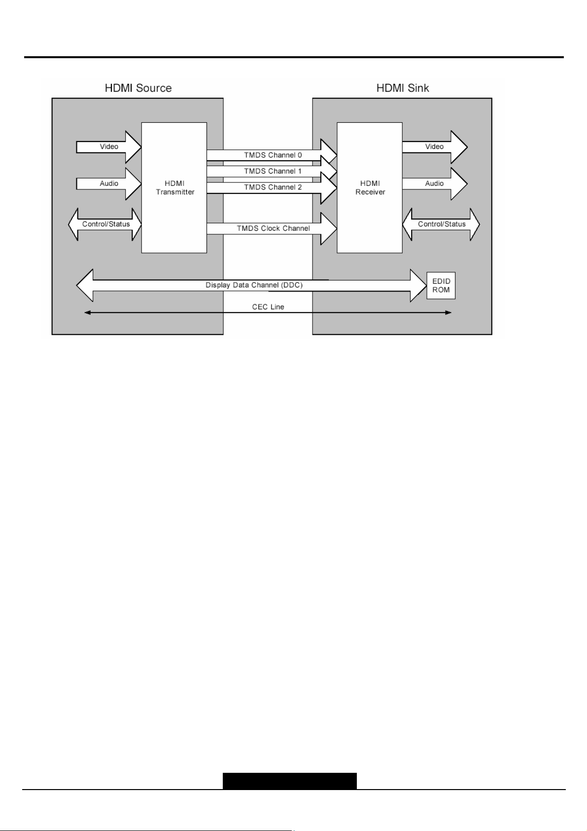
-HDMI system architecture is defined to consist of Sources and Sinks.
A given device may have one or more HDMI inputs and one or more HDMI outputs.
Each HDMI input on these devices shall follow all of the rules for an HDMI Sink
and each HDMI output shall follow all of the rules for an HDMI Source.
- As shown in Figure 12-1 HDMI Block Diagram the HDMI cable and connectors
carry four differential pairs that make up the TMDS data and clock channels.
These channels are used to carry video, audio and auxiliary data. In addition,
HDMI carries a VESA DDC channel. The DDC is used for configuration and status
exchange between a single Source and a single Sink.
The optional CEC protocol provides high-level control functions between
all of the various audiovisual products in a user’s environment.
--20--
Page 22
Marantz Technical Service Manual
12-1 HDMI Block Diagram
- Audio, video and auxiliary data is transmitted across the three TMDS data channels.
The video pixel clock is transmitted on the TMDS clock channel and is used by the
receiver
as a frequency reference for data recovery on the three TMDS data channels.
- Video data is carried as a series of 24-bit pixels on the three TMDS data channels.
TMDS encoding converts the 8 bits per channel into the 10 bit DC-balanced, transition
minimized
sequence which is then transmitted serially across the pair at a rate of 10 bits per pixel
clock period.
- Video pixel rates can range from 25MHz to 165MHz. Video formats with rates below
25MHz
can be transmitted using a pixel-repetition scheme. The video pixels can be encoded in
either RGB,
BCR 4:4:4 or YCBCR 4:2:2 formats. In all three cases, up to 24 bits per pixel can be
YC
transferred.
- Basic audio functionality consists of a single IEC 60958 audio stream at sample rates of
32kHz, 44.1kHz
or 48kHz. This can accommodate any normal stereo stream. Optionally, HDMI can carry a
single such
--21--
Page 23
stream at sample rates up to 192KHz or from two to four such streams (3 to 8 audio
channels) at sample
rates up to 96KHz. HDMI can also carry IEC 61937 compressed (e.g. surround-sound)
stream at sample
rates up to 192kHz.
- The DDC is used by the Source to read the Sink’s Enhanced Extended Display
Identification Data
(E-EDID) in order to discover the Sink.s configuration and/or capabilities.
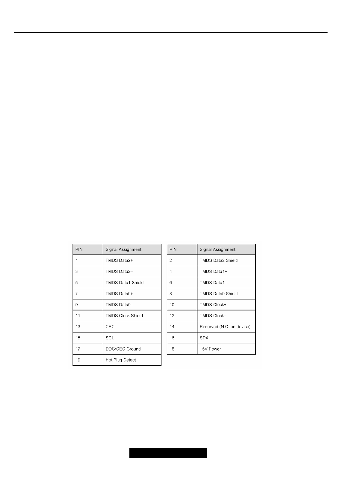
7.3.2 Connectors and Cables
- A device.s external HDMI connection shall be presented via one of the two specified
HDMI connectors,
Type A or Type B. This connector can be attached directly to the device or can be
attached via a cable
adapter that is shipped with the device.
- The Type A connector carries all required HDMI signals, including a single TMDS link.
The Type B
connector is slightly larger and carries a second TMDS link, which is necessary to support
very high-
resolution computer displays requiring dual link bandwidth. A passive cable adapter
between Type A and
Type B connectors is specified.
7.3.3 Connectors Pin Assignment
Type A connector Pin Assingment
--22--
Page 24
Marantz Technical Service Manual
AMS1085
--23--
Page 25
--24--
Page 26
Marantz Technical Service Manual
--25--
Page 27

--26--
Page 28
Audio
8X
De
-
emphasis
8X
Ü
Í DAC
AK4386
Marantz Technical Service Manual
AK4386
ASAHI KASEI [AK4386]
The AK4386 is a 24bit low voltage & low power stereo DAC. The AK4386 uses the Advanced Multi-Bit ∆Σ
architecture, this architecture achieves DR=100dB at 3V operation. The AK4386 integrates a
combination of SCF and CTF filters increasing performance for systems with excessive clock jitter. The
AK4386 is suitable for the portable audio system like MP3 and the home audio systems like STB and TV,
etc as low power and small package. The AK4386 is offered in a space saving 16pin TSSOP package.
o Sampling Rate: 8kHz ¢ 96kHz
o 24-Bit 8 times FIR Digital Filter
o SCF with high tolerance to clock jitter
o Single-ended output buffer
o Digital de-emphasis for 44.1kHz sampling
o I/F Format: 24-Bit MSB justified, 16/24-Bit LSB justified, I2S Compatible
o Master Clock:
o CMOS Input Level
o THD+N: ó86dB
o DR, S/N: 100dB(@VDD=3.0V)
o Power Supply: 2.2 to 3.6V
o Ta = ó40 ¢ 85pC
o 16pin TSSOP
100dB 96kHz 24-Bit 2ch
GENERAL DESCRIPTION
FEATURES
512/768/1024/1536fs for Half Speed (8kHz ¢ 24kHz)
256/384/512/768fs for Normal Speed (8kHz ¢ 48kHz)
128/192/256/384fs for Double Speed (48kHz ¢ 96kHz)
PDN
LRCK
BICK
SDTI
MS0280-E-00 2003/12
Data
Interface
DEMTEST
Control
Interpolator
Interpolator
-1-
MCLK
Clock
Divider
∆Σ
Modulator
∆Σ
Modulator
SCF
CTF
SCF
CTF
VDD
VSS
VCOM
LOUT
ROUT
--27--
Page 29
ASAHI KASEI [AK4386]
nOrdering Guide
AK4386VT
AKD4386 Evaluation Board for AK4386
n Pin Layout
MCLK
BICK
SDTI
LRCK
PDN
DFS0
DFS1
DEM
−40∼
+85°C 16pin TSSOP (0.65mm pitch)
1
2
3
4
Top View
5
6
7
8
16
15
14
13
12
11
10
9
TEST
DIF1
VDD
VSS
VCOM
LOUT
ROUT
DIF0
MS0280-E-00 2003/12
-2-
--28--
Page 30
Marantz Technical Service Manual
ASAHI KASEI [AK4386]
No.Pin Name I/OFunction
1MCLK IMaster Clock Input Pin
2BICK IAudio Serial Data Clock Pin
3SDTI IAudio Serial Data Input Pin
4LRCK IInput Channel Clock Pin
5PDN I
6DFS0 ISampling Speed Select 0 Pin
7DFS1 ISampling Speed Select 1 Pin
8DEM I
9DIF0 IAudio Interface Format 0 Pin
10ROUT O Rch Analog Output Pin
11LOUT O Lch Analog Output Pin
12VCOM O
13VSS -Ground Pin
14VDD 15DIF1 IAudio Interface Format 1 Pin
16TEST I
PIN/FUNCTION
Full Power Down Mode Pin
“L” : Power down, “H” : Power up
De-emphasis Filter Enable Pin
“L” : OFF, “H” : ON (De-emphasis of fs=44.1kHz is enable.)
Common Voltage Output Pin, 0.55 × VDD
Normally connected to VSS with a 4.7µF (min. 1µF, max. 10µF) electrolytic
capacitor.
Power Supply Pin, 2.2 ∼ 3.6V
TEST Pin
This pin should be connected to VDD.
Note: All digital input pins should not be left floating.
n Handling of Unused Pin
The unused output pins should be processed appropriately as below.
Classification Pin Name Setting
Analog LOUT, ROUT This pin should be open.
MS0280-E-00 2003/12
-3-
--29--
Page 31

HY5DU281622ET
HY5DU281622ET
DESCRIPTION
The Hynix HY5DU281622ET is a 134,217,728-bit CMOS Double Data Rate(DDR) Synchronous DRAM, ideally suited for
the point-to-point applications which require high densities and high bandwidth.
The Hynix 8Mx16 DDR SDRAMs offer fully synchronous operations referenced to both rising and falling edges of the
clock. While all addresses and control inputs are latched on the rising edges of the CK (falling edges of the /CK), Data,
Data strobes and Write data masks inputs are sampled on both rising and falling edges of it. The data paths are internally pipelined and 2-bit prefetched to achieve very high bandwidth. All input and output voltage levels are compatible
with SSTL_2.
FEATURES
2.8V +/- 0.1V VDD and VDDQ power supply
supports 400/375/350/333/300MHz
2.5V +/- 5% VDD and VDDQ power supply
supports 275/250/200/166MHz
All inputs and outputs are compatible with SSTL_2
interface
JEDEC Standard 400 mil x 875 mil 66 Pin TSOP II,
with 0.65mm pin pitch
Fully differential clock inputs (CK, /CK) operation
Double data rate interface
Source synchronous - data transaction aligned to
bidirectional data strobe (UDQS,LDQS)
Data outputs on DQS edges when read (edged DQ)
Data inputs on DQS centers when write (centered
DQ)
Data(DQ) and Write masks(DM) latched on the both
rising and falling edges of the data strobe
All addresses and control inputs except Data, Data
strobes and Data masks latched on the rising edges
of the clock
Write mask byte controls by DM (UDM,LDM)
Programmable /CAS Latency 5, 4 and 3 are sup-
ported
Programmable Burst Length 2, 4 and 8 with both
sequential and interleave mode
Internal 4 bank operation with single pulsed /RAS
tRAS Lock-Out function are supported
Auto refresh and self refresh are supported
4096 refresh cycles / 32ms
Full strength, Half strength and Weak Impedance
driver options controlled by EMRS
ORDERING INFORMATION
Part No.
HY5DU281622ET-25
HY5DU281622ET-26375MHz750Mbps/pin
HY5DU281622ET-28350MHz700Mbps/pin
HY5DU281622ET-30333MHz666Mbps/pin
HY5DU281622ET-33300MHz600Mbps/pin
HY5DU281622ET-36
HY5DU281622ET-4250MHz500Mbps/pin
HY5DU281622ET-5200MHz400Mbps/pin
Power
Supply
VDD/VDDQ=2.8V
VDD/VDDQ=2.5V
Clock
Frequency
400MHz800Mbps/pin
275MHz550Mbps/pin
Max Data Rate interface Package
--30--
SSTL_2
400 x 875mil
66 Pin TSOP II
2
Page 32

Marantz Technical Service Manual
PIN CONFIGURATION (Top View)
HY5DU281622ET
VDD
DQ0
VDDQ
DQ1
DQ2
VSSQ
DQ3
DQ4
VDDQ
DQ5
DQ6
VSSQ
DQ7
NC
VDDQ
LDQS
NC
VDD
NC
LDM
/WE
/CAS
/RAS
/CS
NC
BA0
BA1
A10/AP
A0
A1
A2
A3
VDD
1
2
3
4
5
6
7
8
9
10
11
12
13
14
15
16
17
18
0.65mm pin pitch
19
20
21
22
23
24
25
26
27
28
29
30
31
32
33
400mil X 875mil
66pin TSOP -II
66
65
64
63
62
61
60
59
58
57
56
55
54
53
52
51
50
49
48
47
46
45
44
43
42
41
40
39
38
37
36
35
34
VSS
DQ15
VSSQ
DQ14
DQ13
VDDQ
DQ12
DQ11
VSSQ
DQ10
DQ9
VDDQ
DQ8
NC
VSSQ
UDQS
NC
VREF
VSS
UDM
/CK
CK
CKE
NC
NC
A11
A9
A8
A7
A6
A5
A4
VSS
ROW AND COLUMN ADDRESS TABLE
ITEMS 8Mx16
Organization 2M x 16 x 4banks
Row Address A0 - A11
Column Address A0-A8
Bank Address BA0, BA1
Auto Precharge Flag A10
Refresh 4K
--31--
Page 33

PIN DESCRIPTION
PIN TYPE DESCRIPTION
HY5DU281622ET
CK, /CKInput
CKEInput
/CSInput
BA0, BA1Input
A0 ~ A11Input
/RAS, /CAS, /WEInput
UDM, LDMInput
UDQS, LDQS I/O
DQ0 ~ DQ15I/OData input / output pin : Data Bus
VDD/VSS SupplyPower supply for internal circuits and input buffers.
VDDQ/VSSQ SupplyPower supply for output buffers for noise immunity.
V REF SupplyReference voltage for inputs for SSTL interface.
NCNCNo connection.
Clock: CK and /CK are differential clock inputs. All address and control input signals are
sampled on the crossing of the positive edge of CK and negative edge of /CK. Output
(read) data is referenced to the crossings of CK and /CK (both directions of crossing).
Clock Enable: CKE HIGH activates, and CKE LOW deactivates internal clock signals, and
device input buffers and output drivers. Taking CKE LOW provides PRECHARGE POWER
DOWN and SELF REFRESH operation (all banks idle), or ACTIVE POWER DOWN (row
ACTIVE in any bank). CKE is synchronous for POWER DOWN entry and exit, and for SELF
REFRESH entry and exit. CKE is asynchronous for output disable. CKE must be maintained high throughout READ and WRITE accesses. Input buffers, excluding CK, /CK and
CKE are disabled during POWER DOWN. Input buffers, excluding CKE are disabled during
SELF REFRESH. CKE is an SSTL_2 input, but will detect an LVCMOS LOW level after Vdd
is applied.
Chip Select : Enables or disables all inputs except CK, /CK, CKE, DQS and DM. All commands are masked when CS is registered high. CS provides for external bank selection on
systems with multiple banks. CS is considered part of the command code.
Bank Address Inputs: BA0 and BA1 define to which bank an ACTIVE, Read, Write or PRECHARGE command is being applied.
Address Inputs: Provide the row address for ACTIVE commands, and the column address
and AUTO PRECHARGE bit for READ/WRITE commands, to select one location out of the
memory array in the respective bank. A10 is sampled during a precharge command to
determine whether the PRECHARGE applies to one bank (A10 LOW) or all banks (A10
HIGH). If only one bank is to be precharged, the bank is selected by BA0, BA1. The
address inputs also provide the op code during a MODE REGISTER SET command. BA0
and BA1 define which mode register is loaded during the MODE REGISTER SET command
(MRS or EMRS).
Command Inputs: /RAS, /CAS and /WE (along with /CS) define the command being
entered.
Input Data Mask: DM is an input mask signal for write data. Input data is masked when
DM is sampled HIGH along with that input data during a WRITE access. DM is sampled
on both edges of DQS. Although DM pins are input only, the DM loading matches the DQ
and DQS loading. LDM corresponds to the data on DQ0-Q7; UDM corresponds to the data
on DQ8-Q15
Data Strobe: Output with read data, input with write data. Edge aligned with read data,
centered in write data. Used to capture write data. LDQS corresponds to the data on
DQ0-Q7; UDQS corresponds to the data on DQ8-Q15
--32--
Page 34

Marantz Technical Service Manual
K4S643232H
SDRAM 64Mb H-die (x32)
CMOS SDRAM
512K x 32Bit x 4 Banks
FEATURES
? JEDEC standard 3.3V power supply
? LVTTL compatible with multiplexed address
? Four banks operation
? MRS cycle with address key programs
-. CAS latency (2 & 3)
-. Burst length (1, 2, 4, 8 & Full page)
-. Burst type (Sequential & Interleave)
? All inputs are sampled at the positive going edge of the system clock.
? Burst read single-bit write operation
? DQM (x4,x8) & L(U)DQM (x16) for masking
? Auto & self refresh
? 15.6us refresh duty cycle
GENERAL DESCRIPTION
The K4S643232H is 67,108,864 bits synchronous high data rate Dynamic RAM organized as 4 x 524,288 words by 32 bits, fabricated
with SAMSUNG s high performance CMOS technology. Synchronous design allows precise cycle control with the use of system clock.
I/O transactions are possible on every clock cycle. Range of operating frequencies, programmable burst length and programmable
latencies allow the same device to be useful for a variety of high bandwidth, high performance memory system applications.
Ordering Information
Part No. Orgainization Max Freq. Interface Package
K4S643232H-TC/L70512K x 32 143MHzLVTTL86pin TSOP
K4S643232H-TC/L60512K x 32166MHzLVTTL86pin TSOP
K4S643232H-TC/L55512K x 32183MHzLVTTL86pin TSOP
K4S643232H-TC/L50512K x 32200MHzLVTTL86pin TSOP
Organization Row Address Column Address
1Mx32A0~A10A0-A7
Row & Column address configuration
3 -
--33--
Page 35

SDRAM 64Mb H-die (x32)
Package Physical Dimension
CMOS SDRAM
0.10
0.004
MAX
#86
#1
0.61
( )
0.024
#44
#43
22.62
MAX
0.891
22.22
0.20
0.0079
0.875
+0.07
-0.03
0.003
-0.001
0.10
0.004
0.50
0.0197
0.21
0.008
0.05
0.002
86Pin TSOP Package Dimension
1.00
0.039
0.10
0.004
0.25
0.010
0.125
0.005
1.20
0.047
TYP
+0.075
-0.035
+0.003
-0.001
MAX
0.05
0.002
0~8 C
MIN
- 4 -
--34--
Page 36

Marantz Technical Service Manual
SDRAM 64Mb H-die (x32)
FUNCTIONAL BLOCK DIAGRAM
Bank Select
CLK
ADD
Data Input Register
512K x 32
512K x 32
512K x 32
512K x 32
Column Decoder
Latency & Burst Length
CMOS SDRAM
LWE
LDQM
DQi
LCKE
LRASLCBRLWE
CLKCKECS RAS CAS WE DQM
LCASLWCBR
Timing Register
Programming Register
-
--35--
Page 37

SDRAM 64Mb H-die (x32)
PIN FUNCTION DESCRIPTION
Pin Name Input Function
CLK System clock Active on the positive going edge to sample all inputs.
CS Chip select
CKE Clock enable
A0 ~ A10 Address
BA0,1 Bank select address
RAS Row address strobe
CAS Column address strobe
WE Write enable
DQM0 ~ 3 Data input/output mask
DQ0 ~ 31 Data input/output Data inputs/outputs are multiplexed on the same pins.
VDD/VSS Power supply/ground Power and ground for the input buffers and the core logic.
VDDQ/VSSQ Data output power/ground
NC No Connection This pin is recommended to be left No connection on the device.
Disables or enables device operation by masking or enabling all inputs except
CLK, CKE and DQM.
Masks system clock to freeze operation from the next clock cycle.
CKE should be enabled at least one cycle prior to new command.
Disables input buffers for power down mode.
Row/column addresses are multiplexed on the same pins.
Row address : RA0 ~ RA10, Column address : CA0 ~ CA7
Selects bank to be activated during row address latch time.
Selects bank for read/write during column address latch time.
Latches row addresses on the positive going edge of the CLK with RAS low.
Enables row access & precharge.
Latches column addresses on the positive going edge of the CLK with CAS low.
Enables column access.
Enables write operation and row precharge.
Latches data in starting from CAS, WE active.
Makes data output Hi-Z, tSHZ after the clock and masks the output.
Blocks data input when DQM active.
Isolated power supply and ground for the output buffers to provide improved noise
immunity.
CMOS SDRAM
- 7 -
--36--
Page 38

Marantz Technical Service Manual
K6X4008T1F
K6X4008T1F Family CMOS SRAM
512K×8 bit Low Power and Low Voltage CMOS Static RAM
FEATURES
• Process Technology: Full CMOS
• Organization: 512K×8
• Power Supply Voltage: 2.7~3.6V
• Low Data Retention Voltage: 2V(Min)
• Three State Outputs
• Package Type: 32-SOP-525, 32-TSOP2-400F/R
32-TSOP1-0813.4F
GENERAL DESCRIPTION
The K6X4008T1F families are fabricated by SAMSUNG′s
advancedfullCMOS process technology. The families support
various operating temperature range and have various package types for user flexibility of system design. The families also
support low data retention voltage for battery back-up operation
with low data retention current.
PRODUCT FAMILY
Product Family Operating Temperature
K6X4008T1F-B Commercial(0~70°C)
K6X4008T1F-F Industrial(-40~85°C) 10µA
K6X4008T1F-QAutomotive(-40~125°C)
1. This parameter is measured in the voltage range of 3.0V~3.6V with 30pF test load.
2. This parameter is measured with 30pF test load.
Vcc
Range
2.7~3.6V
Speed
551)/702)/85ns
702)/85ns
PIN DESCRIPTION
A18
1
A16
2
3
A14
4
A12
A7
5
A6
6
A5
7
32-SOP
A4
8
32-TSOP2
A3
9
(Forward)
A2
10
A1
11
A0
12
I/O1
13
I/O2
14
I/O3
15
VSS
16
A11
1
A9
2
A8
3
A13
4
WE
5
A17
6
A15
7
VCC
8
A18
9
A16
10
A14
11
A12
12
A7
13
A6
14
A5
15
A4
16
Name Function Name Function
A0~A18 Address Inputs Vcc Power
WE Write Enable Input Vss Ground
CS Chip Select InputI/O1~I/O8 Data Inputs/Outputs
OE Output Enable Input
VCC
32
A15
31
A17
30
WE
29
A13
28
A8
27
A9
26
A11
25
OE
24
23
A10
22
CS
21
I/O8
20
I/O7
19
I/O6
18
I/O5
17
I/O4
32-STSOP1
(Forward)
VCC
A15
A17
WE
A13
A11
A10
I/O8
I/O7
I/O6
I/O5
I/O4
32
31
30
29
28
A8
27
A9
26
32-TSOP2
25
24
23
22
21
20
19
18
17
32
31
30
29
28
27
26
25
24
23
22
21
20
19
18
17
(Reverse)
OE
A10
CS
I/O8
I/O7
I/O6
I/O5
I/O4
VSS
I/O3
I/O2
I/O1
A0
A1
A2
A3
OE
CS
1
A18
A16
2
3
A14
4
A12
A7
5
A6
6
A5
7
A4
8
A3
9
A2
10
A1
11
A0
12
I/O1
13
I/O2
14
I/O3
15
VSS
16
Power Dissipation
Standby
(ISB1, Max)
FUNCTIONAL BLOCK DIAGRAM
Row
Addresses
I/O1 Data
I/O8
CS
WE
OE
10µA
20µA
Control
logic
Operating
(ICC2, Max)
25mA
Clk gen.
Row
select
cont
Data
cont
PKG Type
32-SOP-525, 32-TSOP1-0813.4F
32-TSOP2-400F/R
32-SOP-525, 32-TSOP1-0813.4F
32-TSOP2-400F
Precharge circuit.
Memory array
I/O Circuit
Column select
Column Addresses
SAMSUNG ELECTRONICS CO., LTD. reserves the right to change products and specifications without notice.
2
Revision 1.0
September 2003
--37--
Page 39

K6X4008T1F Family
PRODUCT LIST
Commercial Products(0~70°°C) Industrial Products(-40~85 °°C) Automotive Products(-40~125°°C)
Part Name Function Part Name Function Part Name Function
K6X4008T1F-GB55
K6X4008T1F-GB70
K6X4008T1F-GB85
K6X4008T1F-YB55
K6X4008T1F-YB70
K6X4008T1F-YB85
K6X4008T1F-VB55
K6X4008T1F-VB70
K6X4008T1F-VB85
K6X4008T1F-MB55
K6X4008T1F-MB70
K6X4008T1F-MB85
1. Operating voltage range is 3.0V~3.6V
1)
32-SOP, 55ns, LL
32-SOP, 70ns, LL
32-SOP, 85ns, LL
1)
32-sTSOP1-F, 55ns, LL
32-sTSOP1-F, 70ns, LL
32-sTSOP1-F, 85ns, LL
1)
32-TSOP2-F, 55ns, LL
32-TSOP2-F, 70ns, LL
32-TSOP2-F, 85ns, LL
1)
32-TSOP2-R, 55ns, LL
32-TSOP2-R, 70ns, LL
32-TSOP2-R, 85ns, LL
K6X4008T1F-GF55
K6X4008T1F-GF70
K6X4008T1F-GF85
K6X4008T1F-YF55
K6X4008T1F-YF70
K6X4008T1F-YF85
K6X4008T1F-VF55
K6X4008T1F-VF70
K6X4008T1F-VF85
K6X4008T1F-MF55
K6X4008T1F-MF70
K6X4008T1F-MF85
FUNCTIONAL DESCRIPTION
CS OE WE I/O Mode Power
H
1)
X
L H H High-Z Output Disabled Active
L L H Dout Read Active
L
1. X means don′t care (Must be in low or high state)
1)
X
1)
X
L Din Write Active
1)
32-SOP, 55ns, LL
32-SOP, 70ns, LL
32-SOP, 85ns, LL
1)
32-sTSOP1-F, 55ns, LL
32-sTSOP1-F, 70ns, LL
32-sTSOP1-F, 85ns, LL
1)
32-TSOP2-F, 55ns, LL
32-TSOP2-F, 70ns, LL
32-TSOP2-F, 85ns, LL
1)
32-TSOP2-R, 55ns, LL
32-TSOP2-R, 70ns, LL
32-TSOP2-R, 85ns, LL
K6X4008T1F-GQ70
K6X4008T1F-GQ85
K6X4008T1F-YQ70
K6X4008T1F-YQ85
K6X4008T1F-VQ70
K6X4008T1F-VQ85
32-SOP, 70ns, L
32-SOP, 85ns, L
32-sTSOP1-F, 70ns, L
32-sTSOP1-F, 85ns, L
32-TSOP2-F, 70ns, L
32-TSOP2-F, 85ns, L
High-Z Deselected Standby
ABSOLUTE MAXIMUM RATINGS
1)
Item Symbol Ratings Unit Remark
Voltage on any pin relative to Vss VIN, VOUT -0.2 to VCC+0.3(max. 3.9V) V Voltage on Vcc supply relative to Vss VCC -0.2 to 3.9 V Power Dissipation PD 1.0 W Storage temperature TSTG -65 to 150 °C -
0 to 70 °C K6F4008T1F-B
Operating Temperature TA
-40 to 85 °C K6F4008T1F-F
-40 to 125 °C K6F4008T1F-Q
1. Stresses greater than those listed under "Absolute Maximum Ratings" may cause permanent damage to the device. Functional operation should be
restricted to recommended operating condition. Exposure to absolute maximum rating conditions for extended periods may affect reliability.
--38--
Page 40

Marantz Technical Service Manual
K6X4008T1F Family
-0.2
1)
2)
Vcc+0.2
3)
- 0.6 V
V
RECOMMENDED DC OPERATING CONDITIONS
Item Symbol Min Typ Max Unit
Supply voltage Vcc 2.7 3.0/3.3 3.6 V
Ground Vss 0 0 0 V
Input high voltage VIH 2.2 Input low voltage VIL
Note:
1.Commercial Product: TA=0 to 70°C, otherwise specified
Industrial Product: TA=-40 to 85°C, otherwise specified
Automotive Product: TA=-40 to 125°C, otherwise specified
2. Overshoot: VCC+2.0V in case of pulse width ≤ 30ns
3. Undershoot: -2.0V in case of pulse width ≤ 30ns
4. Overshoot and undershoot are sampled, not 100% tested.
CAPACITANCE
Input capacitance CIN VIN=0V - 8 pF
Input/Output capacitance CIO VIO=0V - 10 pF
1. Capacitance is sampled, not 100% tested.
1)
(f=1MHz, TA=25°C)
Item Symbol Test Condition Min Max Unit
DC AND OPERATING CHARACTERISTICS
Item Symbol Test Conditions Min Typ Max Unit
Input leakage current ILI VIN=Vss to Vcc -1 - 1 µA
Output leakage current ILO CS=VIH or OE=VIH or WE=VIL VIO=Vss to Vcc -1 - 1 µA
Operating power supply current ICC IIO=0mA,CS=VIL, VIN=VIL or VIH, Read - - 2 mA
Cycle time=1µs, 100% duty, IIO=0mACS≤0.2V,VIN≤0.2V or VIN≥Vcc-0.2V
Average operating current
Output low voltage VOL IOL=2.1mA - -0.4 V
Output high voltage VOH IOH=-1.0mA 2.4 - - V
Standby Current(TTL) ISB CS=VIH, Other inputs = VIL or VIH - -0.3mA
Standby Current (CMOS) ISB1 CS≥Vcc-0.2V, Other inputs=0~Vcc
ICC1
Cycle time=Min, 100% duty, IIO=0mA,CS=VIL, VIN=VIHor VIL
ICC2
K6X4008T1F-B - - 10 µA
K6X4008T1F-F - - 10 µA
K6X4008T1F-Q - - 20 µA
- - 3 mA
- - 25mA
--39--
Page 41

K6X4008T1F Family
AC OPERATING CONDITIONS
TEST CONDITIONS(Test Load and Input/Output Reference)
Input pulse level: 0.4 to 2.2V
Input rising and falling time: 5ns
Input and output reference voltage: 1.5V
Output load(see right): CL=100pF+1TTL
1. 55ns,70ns product
CL1)=30pF+1TTL
AC CHARACTERISTICS
(VCC=2.7~3.6V, Commercial product: TA=0 to 70°C, Industrial product: TA=-40 to 85°C, Automotive product: TA=-40 to 125°C)
Parameter List Symbol
Min Max Min Max Min Max
Read cycle time tRC 55 - 70 - 85 - ns
Address access time tAA - 55 - 70 - 85 ns
Chip select to output tCO - 55 - 70 - 85 ns
Output enable to valid output tOE - 25 - 35 - 40 ns
Read
Chip select to low-Z output tLZ 10 - 10 - 10 - ns
Output enable to low-Z output tOLZ 5 - 5 - 5 - ns
Chip disable to high-Z output tHZ 0 20 0 25 0 25 ns
Output disable to high-Z output tOHZ 0 20 0 25 0 25 ns
Output hold from address change tOH 10 - 10 - 10 - ns
Write cycle time tWC 55 - 70 - 85 - ns
Chip select to end of write tCW 45 - 60 - 70 - ns
Address set-up time tAS 0 - 0 - 0 - ns
Address valid to end of write tAW 45 - 60 - 70 - ns
Write pulse width tWP 40 - 55 - 55 - ns
Write
Write recovery time tWR 0 - 0 - 0 - ns
Write to output high-Z tWHZ 0 20 0 25 0 25 ns
Data to write time overlap t DW 25 - 30 - 35 - ns
Data hold from write time tDH 0 - 0 - 0 - ns
End write to output low-Z tOW 5 - 5 - 5 - ns
1. Voltage range is 3.0V~3.6V for commercial and industrial product.
55ns
1)
1)
CL
1. Including scope and jig capacitance
Speed Bins
70ns 85ns
Units
DATA RETENTION CHARACTERISTICS
Item Symbol Test Condition Min
Vcc for data retention VDR CS≥Vcc-0.2V 2.0 - 3.6 V
K6X4008T1F-B -
Data retention current IDR Vcc=3.0V,CS≥Vcc-0.2V
Data retention set-up time tSDR
Recovery time tRDR 5 - -
1. Typical values are measured at TA = 25°C and not 100% tested.
See data retention waveform
K6X4008T1F-F - 10 µA
K6X4008T1F-Q - 20 µA
0 - -
Typ
0.5
1)
Max Unit
10 µA
--40--
ms
Page 42

Marantz Technical Service Manual
MST6151DA-LF
ЪЫЯМЛОЫН
Ч²°«¬-«°°±®¬-«°¬±ЛИЩЯъприрР
Р¿²»´ -«°°±®¬-«°¬±НИЩЯ
Ч²¬»¹®¿¬»¼¬©±у°±®¬¬®·°´»уЯЬЭсРФФ
Ч²¬»¹®¿¬»¼ЬКЧсШЬЭРсШЬУЧ½±³°´·¿²¬®»½»·ª»®
ЗЛКмоо¼·¹·¬¿´ª·¼»±·²°«¬°±®¬Ь«¿´¸·¹¸у¯«¿´·¬§-½¿´·²¹»²¹·²»Ю«·´¬у·²нуЬª·¼»±¼»у·²¬»®´¿½»®
К·¼»±у±ª»®у¹®¿°¸·½РЧР
К·¼»±у¾§у¹®¿°¸·½-°´·¬-½®»»²
УН¬¿®ЯЭЫуо¿¼ª¿²½»¼°·½¬«®»с½±´±® °®±½»--·²¹
»²¹·²»
Ы³¾»¼¼»¼С²у-½®»»²Ь·-°´¿§Э±²¬®±´´»®шСНЬч
»²¹·²»
Ю«·´¬у·²¼«¿´у´·²µФКЬН¬®¿²-³·¬¬»®
луК±´¬¬±´»®¿²¬·²°«¬Ф±©ЫУЧ¿²¼°±©»®-¿ª·²¹º»¿¬«®»Н«°°±®¬-РЙУъЩРС½±²¬®±´ориу°·²РПЪР°¿½µ¿¹»
Я²¿´±¹ОЩЮсЗР¾Р®Ч²°«¬Р±®¬-
Ь«¿´¿²¿´±¹°±®¬--«°°±®¬«°¬±пклУ¸¦
Н«°°±®¬РЭОЩЮ ·²°«¬«°¬±ЛИЩЯакрШ¦
Н«°°±®¬ШЬМКОЩЮсЗР¾Р®сЗЭ¾Э®«°¬±прирР
С²у½¸·°¸·¹¸у°»®º±®³¿²½»РФФН«°°±®¬Э±³°±-·¬»Н§²½¿²¼НСЩ
шН§²½у±²уЩ®»»²ч-»°¿®¿¬±®
Я«¬±³¿¬·½½±´±®½¿´·¾®¿¬·±²
ЬКЧсШЬЭРсШЬУЧЭ±³°´·¿²¬Ч²°«¬Р±®¬
С°»®¿¬»-«°¬±пклУШ¦ш«°¬±ЛИЩЯакрШ¦ч
Н·²¹´»´·²µ±²у½¸·°ЬКЧптр½±³°´·¿²¬®»½»·ª»®
Ш·¹¸у¾¿²¼©·¼¬¸Ь·¹·¬¿´ Э±²¬»²¬Р®±¬»½¬·±²
шШЬЭРчптп½±³°´·¿²¬®»½»·ª»®
Ш·¹¸Ь»º·²·¬·±²У«´¬·³»¼·¿Ч²¬»®º¿½»шШЬУЧч
птр½±³°´·¿²¬®»½»·ª»®©·¬¸ЧоН¿²¼НсРЬЧЪ
¼·¹·¬¿´¿«¼·±±«¬°«¬Ф±²¹у½¿¾´»¬±´»®¿²¬®±¾«-¬®»½»·ª·²¹
Ê·¼»±×²°«¬Ð±®¬
М©±мжожоЮМклкиу¾·¬¼·¹·¬¿´ª·¼»± ·²°«¬°±®¬С²»мжожоЮМкрппку¾·¬¼·¹·¬¿´ª·¼»± ·²°«¬°±®¬
Н«°°±®¬пку¾·¬ЗЛКмжожо·²¬»®´¿½»¼с
°®±¹®»--·ª»ª·¼»±·²°«¬«°¬±прир·сйорР
ß«¬±óݱ²º·¹«®¿¬·±²ñß«¬±óÜ»¬»½¬·±²
Я«¬± ·²°«¬-·¹²¿´º±®³¿¬шНСЩф Э±³°±-·¬»ф
Н»°¿®¿¬»¼ ШНЗТЭфКНЗТЭф¿²¼ЬЫчф¿²¼·²°«¬
³±¼»ш¿´´РЭъМК³±¼»-ч¼»¬»½¬·±²
Я«¬±у¬«²·²¹º«²½¬·±²·²½´«¼·²¹°¸¿-·²¹ф
°±-·¬·±²·²¹ф±ºº-»¬ф ¹¿·²ф¿²¼¶·¬¬»®¼»¬»½¬·±²
Н§²½Ь»¬»½¬·±²º±® ШсКН§²½
Ü«¿´ Ø·¹¸óл®º±®³¿²½»Í½¿´·²¹Û²¹·²»-
Ú«´´§Ð®±¹®¿³³¿¾´»-¸®·²µñ¦±±³½¿°¿¾·´·¬·»Ò±²´·²»¿®ª·¼»±-½¿´·²¹ -«°°±®¬-ª¿®·±«³±¼»-·²½´«¼·²¹Ð¿²±®¿³¿
Ú´»¨·¾´»·²¼»°»²¼»²¬½±²¬®±´ ±º-¸¿®°²»--º±®
ÌÊ¿²¼ ¹®¿°¸·½©·²¼±©-
Ê·¼»±Ð®±½»--·²¹ ú ݱ²ª»®-·±²
íóܳ±¬·±²¿¼¿°¬·ª»ª·¼»±¼»ó·²¬»®´¿½»®©·¬¸
»¼¹»ó±®·»²¬»¼¿¼¿°¬·ª»¿´¹±®·¬¸³º±®-³±±¬¸
´±©ó¿²¹´»»¼¹»ß«¬±³¿¬·½íæî°«´´ó¼±©²úîæî°«´´ó¼±©²
¼»¬»½¬·±²¿²¼ ®»½±ª»®§
Ð×Щ·¬¸°®±¹®¿³³¿¾´»-·¦»¿²¼ ´±½¿¬·±²ô
-«°°±®¬-³«´¬·³»¼·¿¿°°´·½¿¬·±²К·¼»±у±ª»®у¹®¿°¸·½±ª»®´¿§
К·¼»±у¾§у¹®¿°¸·½-°´·¬-½®»»²
Ъ®¿³»®¿¬»½±²ª»®-·±²º±®¾±¬¸³¿·²©·²¼±©
¿²¼-«¾©·²¼±©
УН¬¿® о²¼Щ»²»®¿¬·±²Я¼ª¿²½»¼ Э±´±®Ы²¹·²»
шУН¬¿®ЯЭЫуоч¿«¬±³¿¬·½°·½¬«®»»²¸¿²½»³»²¬
¹·ª»-ж
Þ®·´´·¿²¬¿²¼º®»-¸½±´±®
ײ¬»²-·º·»¼½±²¬®¿-¬¿²¼¼»¬¿·´Ê·ª·¼ -µ·²¬±²»
͸¿®°»¼¹»
Û²¸¿²½»¼¼»°¬¸±ºº·»´¼°»®½»°¬·±²
ß½½«®¿¬»¿²¼·²¼»°»²¼»²¬½±´±®½±²¬®±´
ײ¼»°»²¼»²¬°·½¬«®»½±²¬®±´º±® ¾±¬¸³¿·²
©·²¼±©¿²¼-«¾©·²¼±©
-ÎÙÞ½±³°´·¿²½»¿´´±©-»²¼ó«-»®¬±
»¨°»®·»²½»¬¸»-¿³»½±´±®-¿-ª·»©»¼ ±²ÝÎÌ¿²¼±¬¸»® ¼·-°´¿§Ð®±¹®¿³³¿¾´»ïðó¾·¬ÎÙÞ¹¿³³¿ÝÔËÌ
íóܪ·¼»±²±·-»®»¼«½¬·±²
оррлУН¬¿®Н»³·½±²¼«½¬±®фЧ²½тЯ´´®·¹¸¬-®»-»®ª»¼т
--41--
P
Page 43

Ѳóͽ®»»²ÑÍÜݱ²¬®±´´»®
пксолк½±´±®°¿´»¬¬»
олкслпопу¾·¬с°·¨»´º±²¬
поисолкслпому¾·¬с°·¨»´º±²¬
Н«°°±®¬-¬»¨¬«®»º«²½¬·±²
Н«°°±®¬-мХ¿¬¬®·¾«¬»с½±¼»
Ш±®·¦±²¬¿´¿²¼ª»®¬·½¿´ -¬®»¬½¸±ºСНЬ³»²«Н«°°±®¬-¾«¬¬±²º«²½¬·±²
Р¿¬¬»®²¹»²»®¿¬±®º±® °®±¼«½¬·±²¬»-¬
Н«°°±®¬-СНЬУЛИ¿²¼¿´°¸¿¾´»²¼·²¹
½¿°¿¾·´·¬§
Н«°°±®¬-¾´·²µ·²¹¿²¼ -½®±´´·²¹º±®½´±-»¼
½¿°¬·±²¿°°´·½¿¬·±²-
Ü·¹·¬¿´ß«¼·±×²¬»®º¿½»
ЧоН¼·¹·¬¿´¿«¼·±·²°«¬
ЧоН¼·¹·¬¿´¿«¼·±±«¬°«¬
НсРЬЧЪ¼·¹·¬¿´¿«¼·±±«¬°«¬
ШЬУЧ¿«¼·±½¸¿²²»´ °®±½»--·²¹½¿°¿¾·´·¬§
Р®±¹®¿³³¿¾´»¼»´¿§º±®¿«¼·±сª·¼»±
-§²½¸®±²·¦¿¬·±²
ФКЬНР¿²»´Ч²¬»®º¿½»
Н«°°±®¬-¼«¿´ ´·²µ«°¬±пнлУШ¦ ¼±¬½´±½µº±®
НИЩЯ
Н«°°±®¬-о¼¿¬¿±«¬°«¬º±®³¿¬-жМ¸·²»ъМЧ
¼¿¬¿³¿°°·²¹Э±³°¿¬·¾´»©·¬¸МЧЯсЫЧЯ
Й·¬¸кси¾·¬- ±°¬·±²О»¼«½»¼ -©·²¹º±®ФКЬНº±® ´±©ЫУЧ
Н«°°±®¬-º´»¨·¾´»-°®»¿¼-°»½¬®«³º®»¯«»²½§
©·¬¸нкрШ¦¢пптиУШ¦¿²¼«°¬±олы
³±¼«´¿¬·±²
Û¨¬»®²¿´ ݱ²²»½¬·±²ñݱ³°±²»²¬
Н«°°±®¬-му©·®»¼±«¾´»у¼¿¬¿у®¿¬»¼·®»½¬УЭЛ
¾«ноу¾·¬¼¿¬¿¾«-º±®»¨¬»®²¿´НЬО±®ЬЬО
НЬОЯУº®¿³»¾«ºº»®
Я´´ -§-¬»³½´±½µ- -§²¬¸»-·¦»¼º®±³¿-·²¹´»
»¨¬»®²¿´½´±½µ
ЩЫТЫОЯФЬЫНЭОЧРМЧСТ
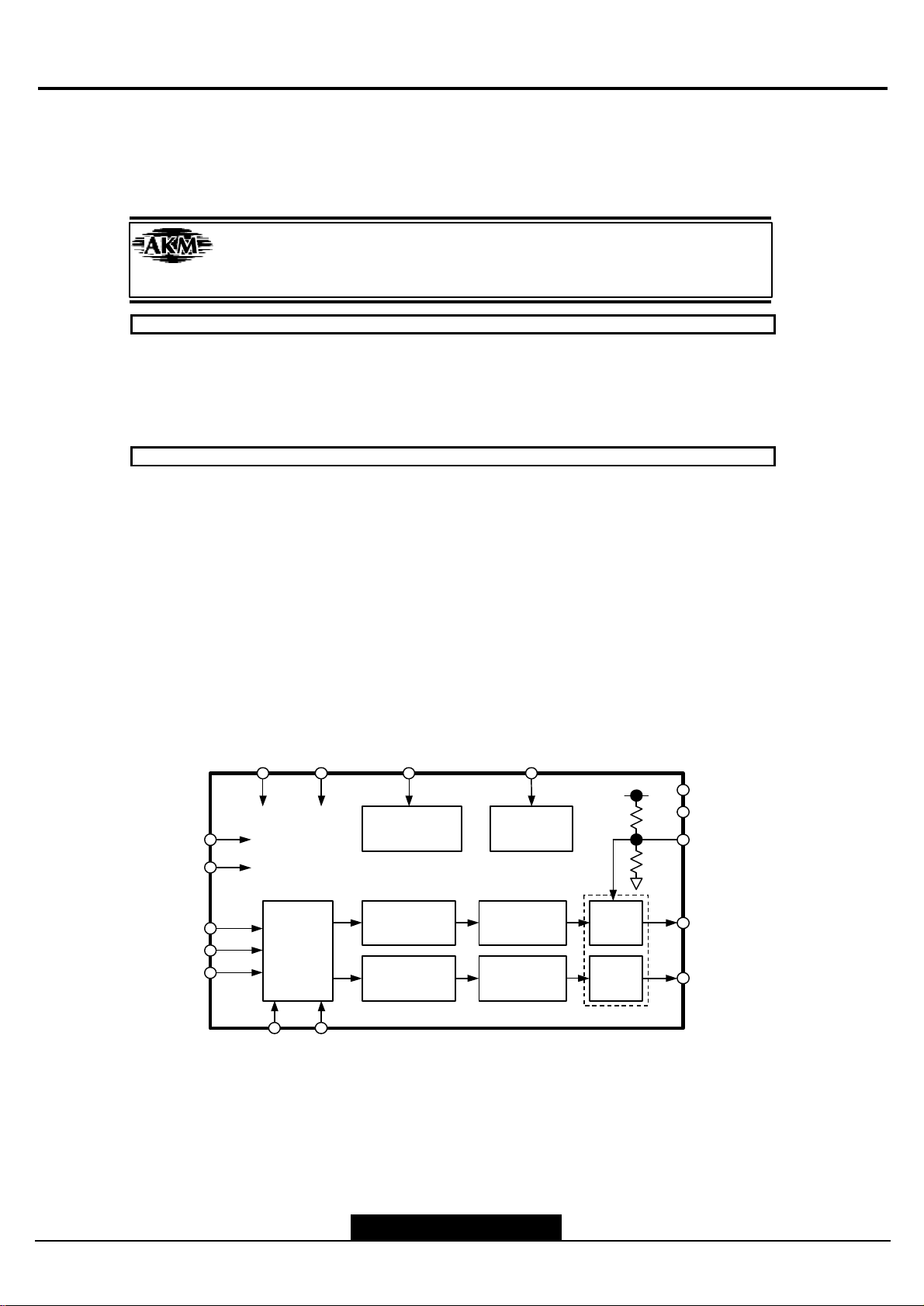
М¸»УНМкплпЬЯ·-¿¸·¹¸°»®º±®³¿²½»¿²¼º«´´§·²¬»¹®¿¬»¼ ¹®¿°¸·½- °®±½»--·²¹ЧЭ-±´«¬·±²º±®³«´¬·уº«²½¬·±²
ФЭЬ³±²·¬±®сМК©·¬¸®»-±´«¬·±²-«°¬±НИЩЯтЧ¬·-½±²º·¹«®»¼©·¬¸¿²·²¬»¹®¿¬»¼¬®·°´»уЯЬЭсРФФф¿²·²¬»¹®¿¬»¼
ЬКЧсШЬЭРсШЬУЧ®»½»·ª»®ф¿ª·¼»±¼»у·²¬»®´¿½»®ф¬©±¸·¹¸¯«¿´·¬§-½¿´·²¹»²¹·²»-ф¿²±²у-½®»»²¼·-°´¿§
½±²¬®±´´»®ф¿²¼¿¾«·´¬у·²±«¬°«¬½´±½µ¹»²»®¿¬±®тЮ§«-»±º»¨¬»®²¿´º®¿³»¾«ºº»®фРЧР·- °®±ª·¼»¼º±®³«´¬·³»¼·¿
¿°°´·½¿¬·±²-тЧ¬-«°°±®¬- ¼»у·²¬»®´¿½»¼º«´´у-½®»»²ª·¼»±фª·¼»±у±²у¹®¿°¸·½±ª»®´¿§ф-°´·¬-½®»»²фº®¿³»®¿¬»
½±²ª»®-·±²ф¿²¼¿-°»½¬®¿¬·±½±²ª»®-·±²º±®ª¿®·±«-ª·¼»± -±«®½»-тМ±º«®¬¸»® ®»¼«½»-§-¬»³½±-¬-ф¬¸»
УНМкплпЬЯ¿´-±·²¬»¹®¿¬»-·²¬»´´·¹»²¬°±©»®³¿²¿¹»³»²¬½±²¬®±´½¿°¿¾·´·¬§º±®¹®»»²у³±¼»®»¯«·®»³»²¬-¿²¼
-°®»¿¼ó-°»½¬®«³-«°°±®¬º±®ÛÓ׳¿²¿¹»³»²¬ò
--42--
Page 44

Marantz Technical Service Manual
РЧТЬЧЯЩОЯУшУНМкплпЬЯч
ÙÒÜ
ЬКЧБЩх
ЬКЧБЩу
ЯКЬЬБЬКЧ
ЬКЧБЮх
ЬКЧБЮу
ÙÒÜ
ЬКЧБЭХх
ЬКЧБЭХу
ЯКЬЬБЬКЧ
ÎÛÈÌ
ЯКЬЬБРФФ
ЩТЬ
ЬЬЭЬБЬЯ
ЬЬЭЬБЭХ
ÙÒÜ
ЯКЬЬБЯЬЭ
ШНЗТЭп
КЗНТЭп
ЮЧТпР
ЮЧТпУ
НСЩЧТп
ЩЧТпР
ЩЧТпУ
ОЧТпР
ОЧТпУ
ЮЧТрУ
ЮЧТрР
ЩЧТрУ
ЩЧТрР
НСЩЧТр
ОЧТрУ
ОЧТрР
ЯКЬЬБЯЬЭ
ÙÒÜ
ШНЗТЭр
КНЗТЭр
ÎÓ×Ü
ÎÛÚÐ
ОЫЪУ
КЧБЬЯМЯЕиГ
КЧБЬЯМЯЕзГ
КЧБЬЯМЯЕпрГ
КЧБЬЯМЯЕппГ
КЧБЬЯМЯЕпоГ
КЧБЬЯМЯЕпнГ
КЧБЬЯМЯЕпмГ
КЧБЬЯМЯЕплГ
ЯКЬЬБЯРФФ
ЩТЬ
ЩРСЕлГ
ЩРСЕмГ
ï
î
í
ì
ë
ê
é
è
ç
ïð
ïï
ïî
ïí
ïì
ïë
ïê
ïé
ïè
ïç
îð
îï
îî
îí
îì
îë
îê
îé
îè
îç
íð
íï
íî
íí
íì
íë
íê
íé
íè
íç
ìð
ìï
ìî
ìí
ìì
ìë
ìê
ìé
ìè
ìç
ëð
ëï
ëî
з² ï
ïëê
ïëë
ïëì
ïëí
ïëî
ïëï
ïëð
ïìç
ïìè
ïìé
ïìê
ïìë
ïìì
ïìí
ïìî
ïìï
ïìð
ïíç
ïíè
ïíé
ïíê
ïíë
ïíì
ïíí
ïíî
ïíï
ïíð
ïîç
ïîè
ïîé
ïîê
ïîë
ïîì
ïîí
ïîî
ïîï
ïîð
ïïç
ïïè
ïïé
ïïê
ïïë
ïïì
ïïí
ïïî
ïïï
ïïð
ïðç
ïðè
ïðé
ïðê
ïðë
КЬЬЭ
ЩТЬ
КЬЬУ
ЬПНЕрГ
УЬЯМЯЕрГ
УЬЯМЯЕпГ
УЬЯМЯЕоГ
УЬЯМЯЕнГ
УЬЯМЯЕмГ
УЬЯМЯЕлГ
УЬЯМЯЕкГ
УЬЯМЯЕйГ
УЬЯМЯЕиГ
УЬЯМЯЕзГ
УЬЯМЯЕпрГ
УЬЯМЯЕппГ
ЩТЬ
КЬЬУ
УЬЯМЯЕпоГ
УЬЯМЯЕпнГ
УЬЯМЯЕпмГ
УЬЯМЯЕплГ
ЬПНЕпГ
ЬПУЕрГ
ЩТЬ
КЬЬЭ
УЯЬОЕппГ
УЯЬОЕпрГ
УЯЬОЕзГ
УЯЬОЕиГ
ЩТЬ
КЬЬУ
УЯЬОЕйГ
УЯЬОЕкГ
УЯЬОЕлГ
УЯЬОЕмГ
УЯЬОЕнГ
УЯЬОЕоГ
УЯЬОЕпГ
УЯЬОЕрГ
ЙЫЖ
ЭЯНЖ
ЩТЬ
КЬЬУ
ОЯНЖ
ЮЯЬОЕрГ
ЮЯЬОЕпГ
ЯКЬЬБРФФо
ЩТЬ
УЭФХ
УЭФХЖ
УЭФХЫ
оррлУН¬¿®Н»³·½±²¼«½¬±®фЧ²½тЯ´´®·¹¸¬-®»-»®ª»¼т
--43--
PDF created with pdfFactory trial version www.pdffactory.com
Page 45

РЧТЬЫНЭОЧРМЧСТ
ÓÝËײ¬»®º¿½»
з²Ò¿³» з²Ì§°» Ú«²½¬·±² з²
ШЙОЫНЫМ Í½¸³·¬¬Ì®·¹¹»®×²°«¬
©ñëÊ󬱴»®¿²¬
ЬЮЛНЕнжрГ ×ñÑ©ñëÊ󬱴»®¿²¬ УЭЛму¾·¬ЬЬОЬ·®»½¬¾«-ем³Я¼®·ª·²¹ -¬®»²¹¬¸ йлуйо
ßÔÛ ×©ñëÊ󬱴»®¿²¬ ÓÝËÞ«-ßÔÛô¿½¬·ª»¸·¹¸ êç
ÎÜÆ ×©ñëÊ󬱴»®¿²¬ ÓÝËÞ«-ÎÜÆô¿½¬·ª»¸·¹¸ éð
ÉÎÆ ×©ñëÊ󬱴»®¿²¬ ÓÝËÞ«-ÉÜÆô¿½¬·ª»¸·¹¸ éï
×ÒÌ Ñ«¬°«¬ ÓÝËÞ«-ײ¬»®®«°¬åì³ß¼®·ª·²¹-¬®»²¹¬¸ êè
Ø¿®¼©¿®»Î»-»¬ô¿½¬·ª»¸·¹¸ êé
ß²¿´±¹×²¬»®º¿½»
з²Ò¿³» з²Ì§°» Ú«²½¬·±² з²
ÎÓ×Ü Ó·¼óͽ¿´»Ê±´¬¿¹»Þ§°¿-- íè
ÎÛÚРײ¬»®²¿´ßÜÝ̱°Ü»ó½±«°´·²¹Ð·² íç
ÎÛÚÓ ×²¬»®²¿´ßÜÝÞ±¬¬±³Ü»ó½±«°´·²¹Ð·² ìð
ÎÛÈÌ ß²¿´±¹ ײ°«¬ Ы¨¬»®²¿´О»-·-¬»®нзр±¸³¬±ЯКЬЬБЬКЧ ïï
ШНЗТЭр ͽ¸³·¬¬Ì®·¹¹»®×²°«¬
©ñëÊ󬱴»®¿²¬
КНЗТЭр ͽ¸³·¬¬Ì®·¹¹»®×²°«¬
©ñëÊ󬱴»®¿²¬
Я²¿´±¹ШНЗТЭЧ²°«¬º®±³Э¸¿²²»´р íê
Я²¿´±¹КНЗТЭЧ²°«¬º®±³Э¸¿²²»´р íé
ЮЧТрУ ß²¿´±¹ ײ°«¬ λº»®»²½»Ù®±«²¼º±®ß²¿´±¹ Þ´«»×²°«¬º®±³Ý¸¿²²»´ð îé
ЮЧТрР ß²¿´±¹ ײ°«¬ ß²¿´±¹ Þ´«»×²°«¬º®±³Ý¸¿²²»´ð îè
ЩЧТрУ ß²¿´±¹ ײ°«¬ λº»®»²½»Ù®±«²¼º±®ß²¿´±¹Ù®»»²×²°«¬º®±³Ý¸¿²²»´ðîç
ЩЧТрР ß²¿´±¹ ײ°«¬ ß²¿´±¹Ù®»»²×²°«¬º®±³Ý¸¿²²»´ð íð
НСЩЧТр ß²¿´±¹ ײ°«¬ ͧ²½Ñ²Ù®»»²×²°«¬º®±³Ý¸¿²²»´ð íï
ОЧТрУ ß²¿´±¹ ײ°«¬ λº»®»²½»Ù®±«²¼º±®ß²¿´±¹Î»¼ ײ°«¬º®±³Ý¸¿²²»´ð íî
ОЧТрР ß²¿´±¹ ײ°«¬ ß²¿´±¹Î»¼ ײ°«¬º®±³Ý¸¿²²»´ð íí
ШНЗТЭп ͽ¸³·¬¬Ì®·¹¹»®×²°«¬
©ñëÊ󬱴»®¿²¬
КНЗТЭп ͽ¸³·¬¬Ì®·¹¹»®×²°«¬
©ñëÊ󬱴»®¿²¬
ЮЧТпУ ß²¿´±¹ ײ°«¬ λº»®»²½»Ù®±«²¼º±®ß²¿´±¹ Þ´«»×²°«¬º®±³Ý¸¿²²»´ï îï
ЮЧТпР ß²¿´±¹ ײ°«¬ ß²¿´±¹ Þ´«»×²°«¬º®±³Ý¸¿²²»´ï îð
НСЩЧТп ß²¿´±¹ ײ°«¬ ͧ²½Ñ²Ù®»»²×²°«¬º®±³Ý¸¿²²»´ï îî
ЩЧТпУ ß²¿´±¹ ײ°«¬ λº»®»²½»Ù®±«²¼º±®ß²¿´±¹Ù®»»²×²°«¬º®±³Ý¸¿²²»´ïîì
Я²¿´±¹ШНЗТЭЧ²°«¬º®±³Э¸¿²²»´п ïè
Я²¿´±¹КНЗТЭЧ²°«¬º®±³Э¸¿²²»´п ïç
оррлУН¬¿®Н»³·½±²¼«½¬±®фЧ²½тЯ´´®·¹¸¬-®»-»®ª»¼т
--44--
Page 46

Marantz Technical Service Manual
з²Ò¿³» з²Ì§°» Ú«²½¬·±² з²
ЩЧТпР ß²¿´±¹ ײ°«¬ ß²¿´±¹Ù®»»²×²°«¬º®±³Ý¸¿²²»´ï îí
ОЧТпУ ß²¿´±¹ ײ°«¬ λº»®»²½»Ù®±«²¼º±®ß²¿´±¹Î»¼ ײ°«¬º®±³Ý¸¿²²»´ï îê
ОЧТпР ß²¿´±¹ ײ°«¬ ß²¿´±¹Î»¼ ײ°«¬º®±³Ý¸¿²²»´ï îë
ÜÊ×ײ¬»®º¿½»
з²Ò¿³» з²Ì§°» Ú«²½¬·±² з²
ЬКЧБОх ײ°«¬ ÜÊ× ×²°«¬Ý¸¿²²»´Î»¼õ îðé
ЬКЧБОу ײ°«¬ ÜÊ× ×²°«¬Ý¸¿²²»´Î»¼ó îðè
ЬКЧБЩх ײ°«¬ ÜÊ× ×²°«¬Ý¸¿²²»´Ù®»»²õî
ЬКЧБЩу ײ°«¬ ÜÊ× ×²°«¬Ý¸¿²²»´Ù®»»²óí
ЬКЧБЮх ײ°«¬ ÜÊ× ×²°«¬Ý¸¿²²»´Þ´«»õë
ЬКЧБЮу ײ°«¬ ÜÊ× ×²°«¬Ý¸¿²²»´Þ´«»óê
ЬКЧБЭХх ײ°«¬ ÜÊ× ×²°«¬Ý´±½µõè
ЬКЧБЭХу ײ°«¬ ÜÊ× ×²°«¬Ý´±½µóç
Ê·¼»±×²¬»®º¿½»
з²Ò¿³» з²Ì§°» Ú«²½¬·±² з²
КЧБЭХ ×²°«¬©ñëÊ󬱴»®¿²¬ Ü·¹·¬¿´Ê·¼»± ײ°«¬Ý´±½µ ëí
КЧБЬЯМЯЕплжрГЧ²°«¬©слКу¬±´»®¿²¬ Ь·¹·¬¿´К·¼»± Ч²°«¬Ь¿¬¿ЕплжрГ миумпфкпулм
Ü·¹·¬¿´ß«¼·±×²¬»®º¿½»
з²Ò¿³» з²Ì§°» Ú«²½¬·±² з²
ЯЛУЭХ Ñ«¬°«¬ ß«¼·± Ó¿-¬»® Ý´±½µÑ«¬°«¬ ïèè
ßËÍÜ Ñ«¬°«¬ ß«¼·±Í»®·¿´Ü¿¬¿Ñ«¬°«¬åì³ß¼®·ª·²¹-¬®»²¹¬¸ ïèç
ЯЛНЭХ Ñ«¬°«¬ ß«¼·±Í»®·¿´Ý´±½µÑ«¬°«¬åì³ß¼®·ª·²¹ -¬®»²¹¬¸ ïçð
ßËÉÍ Ñ«¬°«¬ ɱ®¼Í»´»½¬Ñ«¬°«¬åì³ß¼®·ª·²¹-¬®»²¹¬¸ ïçï
ЯЛУЛМЫ Ñ«¬°«¬ ß«¼·±Ñ«¬°«¬Ó«¬»Ý±²¬®±´ ïçî
НРЬЧЪС Ñ«¬°«¬ НсРЬЧЪЯ«¼·±С«¬°«¬ем³Я¼®·ª·²¹-¬®»²¹¬¸ ïçí
ЯЧУЭХ ×²°«¬ ß«¼·± Ó¿-¬»® Ý´±½µ×²°«¬ ïçê
ß×ÍÜ ×²°«¬ ß«¼·±Í»®·¿´Ü¿¬¿×²°«¬ ïçé
ЯЧНЭХ ×²°«¬ ß«¼·±Í»®·¿´Ý´±½µ×²°«¬ ïçè
ß×ÉÍ ×²°«¬ ɱ®¼Í»´»½¬×²°«¬ ïçç
--45--
Page 47

ФКЬНЧ²¬»®º¿½»
з²Ò¿³» з²Ì§°» Ú«²½¬·±² з²
ФКЯрУ Ñ«¬°«¬ ЯуФ·²µТ»¹¿¬·ª»ФКЬНЬ·ºº»®»²¬·¿´Ь¿¬¿С«¬°«¬ ïéï
ФКЯрР Ñ«¬°«¬ ЯуФ·²µР±-·¬·ª»ФКЬНЬ·ºº»®»²¬·¿´Ь¿¬¿С«¬°«¬ ïéð
ФКЯпУ Ñ«¬°«¬ ЯуФ·²µТ»¹¿¬·ª»ФКЬНЬ·ºº»®»²¬·¿´Ь¿¬¿С«¬°«¬ ïêç
ФКЯпР Ñ«¬°«¬ ЯуФ·²µР±-·¬·ª»ФКЬНЬ·ºº»®»²¬·¿´Ь¿¬¿С«¬°«¬ ïêè
ФКЯоУ Ñ«¬°«¬ ЯуФ·²µТ»¹¿¬·ª»ФКЬНЬ·ºº»®»²¬·¿´Ь¿¬¿С«¬°«¬ ïêé
ФКЯоР Ñ«¬°«¬ ЯуФ·²µР±-·¬·ª»ФКЬНЬ·ºº»®»²¬·¿´Ь¿¬¿С«¬°«¬ ïêê
ФКЯнУ Ñ«¬°«¬ ЯуФ·²µТ»¹¿¬·ª»ФКЬНЬ·ºº»®»²¬·¿´Ь¿¬¿С«¬°«¬ ïêï
ФКЯнР Ñ«¬°«¬ ЯуФ·²µР±-·¬·ª»ФКЬНЬ·ºº»®»²¬·¿´Ь¿¬¿С«¬°«¬ ïêð
ФКЯЭХУ Ñ«¬°«¬ ЯуФ·²µТ»¹¿¬·ª»ФКЬНЬ·ºº»®»²¬·¿´Ь¿¬¿С«¬°«¬ ïêë
ФКЯЭХР Ñ«¬°«¬ ЯуФ·²µР±-·¬·ª»ФКЬНЬ·ºº»®»²¬·¿´Ь¿¬¿С«¬°«¬ ïêì
ФКЮрУ Ñ«¬°«¬ ЮуФ·²µТ»¹¿¬·ª»ФКЬНЬ·ºº»®»²¬·¿´Ь¿¬¿С«¬°«¬ ïèé
ФКЮрР Ñ«¬°«¬ ЮуФ·²µР±-·¬·ª»ФКЬНЬ·ºº»®»²¬·¿´Ь¿¬¿С«¬°«¬ ïèê
ФКЮпУ Ñ«¬°«¬ ЮуФ·²µТ»¹¿¬·ª»ФКЬНЬ·ºº»®»²¬·¿´Ь¿¬¿С«¬°«¬ ïèï
ФКЮпР Ñ«¬°«¬ ЮуФ·²µР±-·¬·ª»ФКЬНЬ·ºº»®»²¬·¿´Ь¿¬¿С«¬°«¬ ïèð
ФКЮоУ Ñ«¬°«¬ ЮуФ·²µТ»¹¿¬·ª»ФКЬНЬ·ºº»®»²¬·¿´Ь¿¬¿С«¬°«¬ ïéç
ФКЮоР Ñ«¬°«¬ ЮуФ·²µР±-·¬·ª»ФКЬНЬ·ºº»®»²¬·¿´Ь¿¬¿С«¬°«¬ ïéè
ФКЮнУ Ñ«¬°«¬ ЮуФ·²µТ»¹¿¬·ª»ФКЬНЬ·ºº»®»²¬·¿´Ь¿¬¿С«¬°«¬ ïéë
ФКЮнР Ñ«¬°«¬ ЮуФ·²µР±-·¬·ª»ФКЬНЬ·ºº»®»²¬·¿´Ь¿¬¿С«¬°«¬ ïéì
ФКЮЭХУ Ñ«¬°«¬ ЮуФ·²µТ»¹¿¬·ª»ФКЬНЬ·ºº»®»²¬·¿´Ь¿¬¿С«¬°«¬ ïéé
ФКЮЭХР Ñ«¬°«¬ ЮуФ·²µР±-·¬·ª»ФКЬНЬ·ºº»®»²¬·¿´Ь¿¬¿С«¬°«¬ ïéê
ÙÐÑײ¬»®º¿½»
з²Ò¿³» з²Ì§°» Ú«²½¬·±² з²
ÐÉÓð Ñ«¬°«¬ ÙÐÑ©·¬¸ÐÉÓÚ«²½¬·±²åì³ß¼®·ª·²¹-¬®»²¹¬¸ îðð
ÐÉÓï Ñ«¬°«¬ ÙÐÑ©·¬¸ÐÉÓÚ«²½¬·±²åì³ß¼®·ª·²¹-¬®»²¹¬¸ îðï
ЩРСЕпГ ×ñÑ ЩРСсЪЧЫФЬ·²°«¬ем³Я¼®·ª·²¹ -¬®»²¹¬¸ éè
ЩРСЕоГ ×ñÑ ЩРСсЬ·¹·¬¿´КНЗТЭЧ²°«¬ем³Я¼®·ª·²¹ -¬®»²¹¬¸ éé
ЩРСЕнГ ×ñÑ ЩРСсЬЬЭ Э´±½µº±®ОСУ éê
ЩРСЕмГ ×ñÑ ЩРСсЬЫЧ²°«¬ем³Я¼®·ª·²¹ -¬®»²¹¬¸ ëî
ЩРСЕлГ ×ñÑ ЩРСсЬ·¹·¬¿´ШНЗТЭЧ²°«¬ем³Я¼®·ª·²¹-¬®»²¹¬¸ ëï
оррлУН¬¿®Н»³·½±²¼«½¬±®фЧ²½тЯ´´®·¹¸¬-®»-»®ª»¼т
--46--
Page 48

Marantz Technical Service Manual
ЬОЯУЧ²¬»®º¿½»
з²Ò¿³» з²Ì§°» Ú«²½¬·±² з²
УКОЫЪ ×²°«¬ О»º»®»²½»К±´¬¿¹»º±®ЬЬОНЬОЯУЧ²¬»®º¿½»прм
УЭФХЫ Ñ«¬°«¬ ЬОЯУУ»³±®§Э´±½µЫ²¿¾´» ïðë
УЭФХЖ Ñ«¬°«¬ ЬОЯУУ»³±®§½´±½µЭ±³°´»³»²¬¿®§сЧ²°«¬
øº±® ¼·ºº»®»²¬·¿´½´±½µ-÷
ÓÝÔÕ Ñ«¬°«¬ ЬОЯУУ»³±®§Э´±½µ ïðé
ÎßÍÆ Ñ«¬°«¬ α©ß¼¼®»--ͬ®±¾»ô¿½¬·ª»´±© ïïî
ÝßÍÆ Ñ«¬°«¬ ݱ´«³²ß¼¼®»--ͬ®±¾»ô¿½¬·ª»´±© ïïë
ÉÛÆ Ñ«¬°«¬ É®·¬»Û²¿¾´»ô¿½¬·ª»´±© ïïê
ЬПУЕпжрГ Ñ«¬°«¬ Ü¿¬¿Ó¿-µÞ§¬»Û²¿¾´» прпфпнн
ЬПНЕнжрГ Ñ«¬°«¬ Ü¿¬¿Í¬®±¾» ипфпррфпнмфплн
ЮЯЬОЕпжрГ Ñ«¬°«¬ Ó»³±®§Þ¿²µß¼¼®»-- ппрфппп
УЯЬОЕппжрГ Ñ«¬°«¬ Ó»³±®§ß¼¼®»-- пнрупойфпомуппй
УЬЯМЯЕнпжрГ ×ñÑ Ó»³±®§Ü¿¬¿ иоуилфииуззф
ïðê
пнлупнифпмпупло
Ó·-½òײ¬»®º¿½»
з²Ò¿³» з²Ì§°» Ú«²½¬·±² з²
È×Ò Ý®§-¬¿´Ñ-½·´´¿¬±®×²°«¬Ý®§-¬¿´Ñ-½·´´¿¬±®×²°«¬ îðí
ÈÑËÌ Ý®§-¬¿´Ñ-½·´´¿¬±®Ñ«¬°«¬Ý®§-¬¿´Ñ-½·´´¿¬±®Ñ«¬°«¬ îðî
ЬЬЭЬБЬЯ ×ñÑ©ñëÊ󬱴»®¿²¬ ШЬЭРН»®·¿´Ю«-Ь¿¬¿сЬЬЭ¼¿¬¿±ºЬКЧ °±®¬ем³Я¼®·ª·²¹
-¬®»²¹¬¸
ЬЬЭЬБЭХ Ч²°«¬©слКуМ±´»®¿²¬ ШЬЭРН»®·¿´Ю«- Э´±½µсЬЬЭ Э´±½µ±ºЬКЧР±®¬ ïë
ЬЬЭОБЬЯ ×ñÑ©ñëÊ󬱴»®¿²¬ ÜÜÝÜ¿¬¿º±®ÎÑÓ êî
ЮЗРЯНН Ú±®Û¨¬»®²¿´ Þ§°¿-- Ý¿°¿½·¬±® ïëè
ïì
б©»®Ð·²-
з²Ò¿³» з²Ì§°» Ú«²½¬·±² з²
ЯКЬЬБЬКЧ нтнКР±©»® ÜÊ×б©»® ìôïð
ЯКЬЬБЯЬЭ нтнКР±©»® ßÜÝб©»® пйфнм
ЯКЬЬБРФФ нтнКР±©»® ÐÔÔб©»® ïî
ЯКЬЬБРФФо нтнКР±©»® ÐÔÔб©»® ïðç
ЯКЬЬБЯРФФ птиКР±©»® ß«¼·±ÐÔÔб©»® ìç
ЯКЬЬБУРФФ нтнКР±©»® ÐÔÔб©»® îðì
оррлУН¬¿®Н»³·½±²¼«½¬±®фЧ²½тЯ´´®·¹¸¬-®»-»®ª»¼т
--47--
Page 49

S29AL008D
This document has not been approved. Sharing this document with non-Spansion employees violates QS9000/TS16949 requirements.
S29AL008D
8 Megabit (1 M x 8-Bit/512 K x 16-Bit)
CMOS 3.0 Volt-only Boot Sector Flash Memory
Data Sheet
Distinctive Characteristics
Architectural Advantage
Single power supply operation
?.7 to 3.6 volt read and write operations for battery-
powered applications
Manufactured on 200nm process technology
ompatible with 0.32 and 230nm Am29LV160 뾅탆
devices
Flexible sector architecture
ne 16 Kbyte, two 8 Kbyte, one 32 Kbyte, and fifteen 뾑
64 Kbyte sectors (byte mode)
ne 8 Kword, two 4 Kword, one 16 Kword, and fifteen 뾑
32 Kword sectors (word mode)
upports full chip erase뾖
ector Protection features:뾖
hardware method of locking a sector to prevent 뾃
any program or erase operations within that sector
ectors can be locked in-system or via programming 뾖
equipment
emporary Sector Unprotect feature allows code 뾗
changes in previously locked sectors
Unlock Bypass Program Command
educes overall programming time when issuing 뾕
multiple program command sequences
Top or bottom boot block configurations
available
Embedded Algorithms
mbedded Erase algorithm automatically 뾇
preprograms and erases the entire chip or any
combination of designated sectors
mbedded Program algorithm automatically writes 뾇
and verifies data at specified addresses
Compatibility with JEDEC standards
inout and software compat뾒 ible with single-power
supply Flash
uperior inadvertent write protection뾖
Performance Characteristics
High performance
ccess times as fast as 55 ns뾃
xtended temperature range (-40 to +125)뾇캜캜
Ultra low power consumption (typical values
at 5 MHz)
?00 nA Automatic Sleep mode current
?00 nA standby mode current
? mA read current
?5 mA program/erase current
Cycling endurance: 1,000,000 cycles per
sector typical
Data retention: 20 years typical
eliable operation for the life of the system뾕
Package option
48-ball FBGA
48-pin TSOP
44-pin SO
Software Features
Data# Polling and toggle bits
rovides a software method of detecting program or 뾒
erase operation completion
Erase Suspend/Erase Resume
uspends an erase operation to read data from, or 뾖
program data to, a sector that is not being erased,
then resumes the erase operation
Hardware Features
Ready/Busy# pin (RY/BY#)
rovides a hardware method of detecting program or 뾒
erase cycle completion
Hardware reset pin (RESET#)
ardware method to reset the device to reading array 뾊
data
--48--
PDF created with pdfFactory trial version www.pdffactory.com
Page 50

Marantz Technical Service Manual
2
Notice On Data Sheet Designations
Spansion LLC issues data sheets with Advance Information or Preliminary designations to advise
readers of product information or intended specifications throughout the product life cycle, including development, qualification, initial production, and full production. In all cases, however,
readers are encouraged to verify that they have the latest information before finalizing their design. The following descriptions of Spansion data sheet designations are presented here to highlight their presence and definitions.
Advance Information
The Advance Information designation indicates that Spansion LLC is developing one or more specific products, but has not committed any design to production. Information presented in a document with this designation is likely to change, and in some cases, development on the product
may discontinue. Spansion LLC therefore places the following conditions upon Advance Information content:
his document contains information on one or more products under development at Spansion LLC. The 밫
information is intended to help you evaluate this product. Do not design in this product without contacting the factory. Spansion LLC reserves the right to change or discontinue work on this proposed
product without notice.
Preliminary
The Preliminary designation indicates that the product development has progressed such that a
commitment to production has taken place. This designation covers several aspects of the product life cycle, including product qualification, initial production, and the subsequent phases in the
manufacturing process that occur before full production is achieved. Changes to the technical
specifications presented in a Preliminary document should be expected while keeping these aspects of production under consideration. Spansion places the following conditions upon Preliminary content:
his document states the current technical specifications regarding the Spansion product(s) described 밫
herein. The Preliminary status of this document indicates that product qualification has been completed,
and that initial production has begun. Due to the phases of the manufacturing process that require
maintaining efficiency and quality, this document may be revised by subsequent versions or modifications due to changes in technical specifications.
Combination
Some data sheets will contain a combination of products with different designations (Advance Information, Preliminary, or Full Production). This type of document will distinguish these products
and their designations wherever necessary, typically on the first page, the ordering information
page, and pages with DC Characteristics table and AC Erase and Program table (in the table
notes). The disclaimer on the first page refers the reader to the notice on this page.
Full Production (No Designation on Document)
When a product has been in production for a period of time such that no changes or only nominal
changes are expected, the Preliminary designation is removed from the data sheet. Nominal
changes may include those affecting the number of ordering part numbers available, such as the
addition or deletion of a speed option, temperature range, package type, or VIO range. Changes
may also include those needed to clarify a description or to correct a typographical error or incorrect specification. Spansion LLC applies the following conditions to documents in this category:
his document states the current technical specifications regarding the Spansion product(s) described 밫
herein. Spansion LLC deems the products to have been in sufficient production volume such that subsequent versions of this document are not expected to change. However, typographical or specification
corrections, or modifications to the valid combinations offered may occur.
--49--
Page 51

General Description
The S29AL008D is an 8 Mbit, 3.0 volt-only Flash memory organized as 1,048,576
bytes or 524,288 words. The device is offered in 48-ball FBGA, 44-pin SO, and
48-pin TSOP packages. For more information, refer to publication number 21536.
The word-wide data (x16) appears on DQ15Q0; the byte-wide (x8) data ap뺻 -
pears on DQ7Q0. This device requires only a single, 3.0 volt V뺻
perform read, program, and erase operations. A standard EPROM programmer
can also be used to program and erase the device.
This device is manufactured using Spansion 200nm process technology, and of뭩 -
fers all the features and benefits of the Am29LV800B, which was manufactured
using 0.32 process technology. 탆
The standard device offers access times of 70, 90, and 120 ns, allowing high
speed microprocessors to operate without wait states. To eliminate bus contention the device contains separate chip enable (CE#), write enable (WE#) and
output enable (OE#) controls.
The device requires only a single 3.0 volt power supply for both read and write
functions. Internally generated and regulated voltages are provided for the program and erase operations.
The device is entirely command set compatible with the JEDEC single-power-
supply Flash standard. Commands are written to the command register using
standard microprocessor write timings. Register contents serve as input to an internal state-machine that controls the erase and programming circuitry. Write
cycles also internally latch addresses and data needed for the programming and
erase operations. Reading data out of the device is similar to reading from other
Flash or EPROM devices.
Device programming occurs by executing the program command sequence. This
initiates the Embedded Program algorithmn internal algorithm that auto뾞 -
matically times the program pulse widths and verifies proper cell margin. The
Unlock Bypass mode facilitates faster programming times by requiring only two
write cycles to program data instead of four.
Device erasure occurs by executing the erase command sequence. This initiates
the Embedded Erase algorithmn internal algorithm that automatically 뾞
preprograms the array (if it is not already programmed) before executing the
erase operation. During erase, the device automatically times the erase pulse
widths and verifies proper cell margin.
The host system can detect whether a program or erase operation is complete by
observing the RY/BY# pin, or by reading the DQ7 (Data# Polling) and DQ6 (toggle) status bits. After a program or erase cycle is completed, the device is ready
to read array data or accept another command.
The sector erase architecture allows memory sectors to be erased and reprogrammed without affecting the data contents of other sectors. The device is fully
erased when shipped from the factory.
Hardware data protection measures include a low VCC detector that automat-
ically inhibits write operations during power transitions. The hardware sector
protection feature disables both program and erase operations in any combination of the sectors of memory. This can be achieved in-system or via
programming equipment.
Data Sheet
supply to
CC
--50--
PDF created with pdfFactory trial version www.pdffactory.com
Page 52

Marantz Technical Service Manual
The Erase Suspend feature enables the user to put erase on hold for any period
of time to read data from, or program data to, any sector that is not selected for
erasure. True background erase can thus be achieved.
The hardware RESET# pin terminates any operation in progress and resets the
internal state machine to reading array data. The RESET# pin may be tied to the
system reset circuitry. A system reset would thus also reset the device, enabling
the system microprocessor to read the boot-up firmware from the Flash memory.
The device offers two power-saving features. When addresses are stable for a
specified amount of time, the device enters the automatic sleep mode. The
system can also place the device into the standby mode. Power consumption is
greatly reduced in both these modes.
Spansion Flash technology combines years of Flash memory manufacturing ex뭩 -
perience to produce the highest levels of quality, reliability and cost
effectiveness. The device electrically erases all bits within a sector simultaneously via Fowler-Nordheim tunneling. The data is programmed using hot
electron injection.
Data Sheet
--51--
PDF created with pdfFactory trial version www.pdffactory.com
Page 53

TCMN3080DA29A
NTSCELECTRONIC2IN1TUNER
SPECIFICATION
1.APPLICATIONS
1-1.ReceivingSystem:(NTSCM)
1-2.ChannelVHF:LowCH.(2)~(B)
1-3.IntermediateFrequencyPIF:(45.75)MHz
1-4.InputImpedance:UHF/VHFTerminal(75) ,Unbalanced
OutputImpedance:(75) ,Unbalanced
1-5.BandChange-OverSystem:(PLLControlSystem)
1-6.TuningSystem:(ElectronicTuningSystemWithPLL)
2.RATINGSANDTESTCONDITIONS
Measurementmustbeexecutedundertheambientconditionsoftheroom
temperatureandhumidity.(Temp.25 2 ,Humidity65 5%RH)
Thefollowingconditionsshallbeappliedforthemeasurementof
electricalcharacteristics.
2-1.EnvironmentConditions
HighCH.(C)~(W+11)
UHF:CH.(W+12)~(69)
CIF:(42.17)MHz
SIF:(41.25)MHz
-.StorageTemperature:-20 C~+70 C
-.OperationTemperature:-5 C~+65 C
-.Relativehumidity:95%MAX.
--52--
Page 54

Marantz Technical Service Manual
NTSCELECTRONIC2IN1TUNER
SPECIFICATION
2-2VoltageCurrentandFunctionsAtEachTerminalandOperationGuaranteed
PIN
NO.
TERMINAL
NAME
OPERATION
SUPPLY
VOLTAGE
FOR
GUARANTEED
VOLTAGE
CURRENT FUNCTIONS
1~4 N.C
5 IFOUT
6 N.C
7 N.C
8 AGCOUT
9 SAS
10 SCL
11 SDA
12 B+
- - -
IFTestPin
- - -
- - -
- - - AGCVOLT.OUT
- - - IICAddressSelect
- - - IICSerialClock
- - - IICSerialData
5V 0.1V 5V 5%
170mAMAX
(150mATYP)
SupplyVoltage
ForTunerBlock
13 SIF
14 -
15 AUDIOOUT
16 AFTOUT
17 VIDEOOUT
- - - SoundIF
- - -
- - - AudioSignalOut
- - - AFTVOLT.OUT
CompositeVideo
BasebandSignalOut
--53--
Page 55

TEA6422
² ê ͬ»®»± ײ°«¬-
² í ͬ»®»± Ñ«°«¬-
² Ù¿·² ݱ²¬®±´ ð ¼ÞñÓ«¬» º±® »¿½¸ Ñ«¬°«¬
² Ý¿-½¿¼¿¾´» øî ¼·ºº»®»²¬ ¿¼¼®»--»-÷
² Í»®·¿´ Þ«- ݱ²¬®±´´»¼
² Ê»®§ Ô±© Ò±·-»
² Ê»®§ Ô±© Ü·-¬±®-·±²
² Ú«´´§ ÛÍÜ Ð®±¬»½¬»¼
² É·¼» ß«¼·± ܧ²¿³·½ ο²¹» ø í Ê
ЬЫНЭОЧРМЧСТ
М¸» МЫЯкмоо -©·¬½¸»- к -¬»®»± ¿«¼·± ·²°«¬- ±² н
-¬»®»± ±«¬°«¬-ò
ß´´ ¬¸» -©·¬½¸·²¹ °±--·¾·´·¬·»- ¿®» ½¸¿²¹»¼ ¬¸®±«¹¸
¬¸» ×îÝ ÞËÍò
ÎÓÍ
МЫЯкмоо
ЮЛНуЭСТМОСФФЫЬ ЯЛЬЧС УЯМОЧИ
НШОЧТХ ЬЧРом
ø͸®·²µ д¿-¬·½ п½µ¿¹»÷
÷
СОЬЫО ЭСЬЫж МЫЯкмоо
ÍÑîè
øд¿-¬·½ Ó±²±°¿½µ¿¹»÷
Ъ·¹«®» пт РЧТ ЭСТТЫЭМЧСТН
НЬЧРом
ï
ÙÒÜ
ЭЯРЯЭЧМЯТЭЫ
ФСЛМп
ОСЛМп
ФСЛМо
î
í
Ê
Í
ì
Ôï
ë
Ôî
ê
Ôí
é
Ôì
è
Ôë
ç
Ôê
ïð
ïï
ïî
СОЬЫО ЭСЬЫж МЫЯкмооЬ
ÍÑîè
ÒÝ
ÒÝ
ï
î
í
Ê
Í
ì
Ôï
ë
Ôî
ê
Ôí
é
è
ç
Ôì
ïð
Ôë
ïï
Ôê
ïî
ïí
ïì
ÙÒÜ
îì
ÍÜß
îí
ÍÝÔ
îî
ßÜÜÎ
îï
Îï
îð
Îî
ïç
Îí
ïè
Îì
ïé
Îë
ïê
Îê
ïë
ОСЛМн
ïì
ФСЛМн
ïí
ОСЛМо
ЭЯРЯЭЧМЯТЭЫ
ФСЛМп
ОСЛМп
îè
ÍÜß
îé
ÍÝÔ
îê
ßÜÜÎ
îë
Îï
îì
Îî
îí
Îí
îî
ÒÝ
îï
ÒÝ
îð
Îì
ïç
Îë
ïè
Îê
ïé
ОСЛМн
ïê
ФСЛМн
ïë
ОСЛМоФСЛМо
--54--
Page 56

Marantz Technical Service Manual
МЫЯкмоо
ЮФСЭХ ЬЧЯЩОЯУ
ОЧЩШМ ЧТРЛМН
Ùß×Ò ã ð ¼Þ
ОЧЩШМ
СЛМРЛМН
Ê
Í
Ý
НЛРРФЗ
ЮЛН ЬЫЭСЬЫО
ÙÒÜ
Ùß×Ò ã ð ¼Þ
ФЫЪМ ЧТРЛМН
ЯЮНСФЛМЫ УЯИЧУЛУ ОЯМЧТЩН
ͧ³¾±´ п®¿³»¬»® Ê¿´«» ˲·¬
Ê
ÝÝ
Ì
±°»®
Ì
-¬¹
Í«°°´§ ʱ´¬¿¹» ïî Ê
Ñ°»®¿¬·²¹ Ì»³°»®¿¬«®» ðô õ éð
ͬ±®¿¹» Ì»³°»®¿¬«®» ó îðô õ ïëð
ÍÜß
ÍÝÔ
ßÜÜÎ
ФЫЪМ
СЛМРЛМН
±
Ý
±
Ý
МШЫОУЯФ ЬЯМЯ
ͧ³¾±´ п®¿³»¬»® Ê¿´«» ˲·¬
ά¸ø¶ó¿÷Ö«²½¬·±² ó ¿³¾·»²¬ ̸»®³¿´ λ-·-¬¿²½»
НЬЧРом
НСои
éë
éë
--55--
±
ÝñÉ
±
ÝñÉ
Page 57

ЫФЫЭМОЧЭЯФ ЭШЯОЯЭМЫОЧНМЧЭН
Ìßã îë±Ýô ÊÍã çÊô ÎÔã ïðµÉô ÎÙã êðð Éô º ã ïµØ¦ ø«²´»-- ±¬¸»®©·-» -°»½·º·»¼÷
ͧ³¾±´ п®¿³»¬»® Ì»-¬ ݱ²¼·¬·±²- Ó·²ò ̧°ò Ó¿¨ò ˲·¬
НЛРРФЗ
Ê
Í
×
Í
ÍÊΠη°°´» 붻½¬·±² Ê×Ò ã ëðð³Ê
Í«°°´§ ʱ´¬¿¹» è ïðïï Ê
Í«°°´§ Ý«®®»²¬ í è ³ß
ô º ã ïµØ¦ éð èð ¼Þ
ÎÓÍ
УЯМОЧИ
Ê
×Ò
Î
×
Ý
Í
ײ°«¬ ÜÝ Ô»ª»´ Ê
ñî Ê
ÝÝ
ײ°«¬ λ-·-¬¿²½» íð ëð ïðð µ
ݸ¿²²»´ Í»°¿®¿¬·±² Ê×Ò ã îÊ
ô º ã ïµØ¦ èð çð ¼Þ
ÎÓÍ
СЛМРЛМ ЮЛЪЪЫО
Ê
ÑËÌ
Î
ÑËÌ
С«¬°«¬ ЬЭ Ф»ª»´ КЭЭсо К
Ñ«¬°«¬ λ-·-¬¿²½» ëð ïðð É
»Ò× ×²°«¬ Ò±·-» ÞÉ ã îð ó îðµØ¦ô º´¿¬ í kÊ
ÍñÒ Í·¹²¿´ ¬± Ò±·-» ο¬·± Ê×Ò ã Ê
ÑËÌ
ã ïÊ
ÎÓÍ
ïïð ¼Þ
Ù Ù¿·² óï ð õ ï ¼Þ
¼ Ü·-¬±®¬·±² Ê×Ò ã Ê
Ê
ÝÔ
Î
Ô
Ý´·°°·²¹ Ô»ª»´ ¼ ã ðòí ûô ÊÍ ã ïð Ê îòè í Ê
Ñ«¬°«¬ Ô±¿¼ λ-·-¬¿²½» î µ
ÑËÌ
ã ïÊ
ÎÓÍ
ðòðï ðòðë û
МЫЯкмоо
É
ÎÓÍ
É
--56--
Page 58

Marantz Technical Service Manual
МЫЯкмоо
ЧоЭ ЮЛН ЭШЯОЯЭМЫОЧНМЧЭН
ͧ³¾±´ п®¿³»¬»®
ÍÝÔ
Ê
×Ô
Ê
×Ø
×
Ô×
º
ÍÝÔ
¬
Î
¬
Ú
Ý
×
ÍÜß
Ê
×Ô
Ê
×Ø
×
Ô×
Ý
×
¬
Î
¬
Ú
Ê
ÑÔ
¬
Ú
Ý
Ô
МЧУЧТЩ
¬
ÔÑÉ
¬
Ø×ÙØ
¬ÍËô ÜßÌ Ü¿¬¿ Í»¬ó«° Ì·³» îë𠲬ØÜô ÜßÌ Ü¿¬¿ ر´¼ Ì·³» ð íì𠲬ÍËô ÍÌÑ Í»¬ó«° Ì·³» º®±³ Ý´±½µ Ø·¹¸ ¬± ͬ±° ìòð k-
¬
ÞËÚ
¬ØÜô ÍÌß Í¬¿®¬ ر´¼ Ì·³» ìòð k-
¬ÍËô ÍÌß
Ô±© Ô»ª»´ ײ°«¬ ʱ´¬¿¹» ó ðòí õ ïòë Ê
Ø·¹¸ Ô»ª»´ ײ°«¬ ʱ´¬¿¹» íòð ÊÝÝ õ ðòë Ê
ײ°«¬ Ô»¿µ¿¹» Ý«®®»²¬ Ê× ã 𠬱 Ê
Ý´±½µ Ú®»¯«»²½§ ð ïðð µØ¦
ײ°«¬ η-» Ì·³» ïòëÊ ¬± íÊ ïððð ² ×²°«¬ Ú¿´´ Ì·³» íÊ ¬± ïòëÊ íðð ² ×²°«¬ Ý¿°¿½·¬¿²½» ïð °Ú
Ô±© Ô»ª»´ ײ°«¬ ʱ´¬¿¹» ó ðòí õ ïòë Ê
Ø·¹¸ Ô»ª»´ ײ°«¬ ʱ´¬¿¹» íòð ÊÝÝ õ ðòë Ê
ײ°«¬ Ô»¿µ¿¹» Ý«®®»²¬ Ê× ã 𠬱 Ê
ײ°«¬ Ý¿°¿½·¬¿²½» ïð °Ú
ײ°«¬ η-» Ì·³» ïòëÊ ¬± íÊ ïððð ² ×²°«¬ Ú¿´´ Ì·³» íÊ ¬± ïòëÊ íðð ² Ô±© Ô»ª»´ Ñ«¬°«¬ ʱ´¬¿¹» ×ÑÔ ã í³ß ðòì Ê
Ñ«¬°«¬ Ú¿´´ Ì·³» íÊ ¬± ïòëÊ îëð ²-
Ô±¿¼ Ý¿°¿½·¬¿²½» ìðð °Ú
Ý´±½µ Ô±© л®·±¼ ìòé k Ý´±½µ Ø·¹¸ л®·±¼ ìòð k-
ͬ¿®¬ Í»¬ó«° Ì·³» º±´´±©·²¹ ¿ ͬ±° ìòé k-
ͬ¿®¬ Í»¬ó«° Ì·³» º±´´±©·²¹ Ý´±½µ Ô±©ó¬± Ø·¹¸
Ì®¿²-·¬·±²
Ì»-¬
ݱ²¼·¬·±²-
ÝÝ
ÝÝ
Ó·²ò Ó¿¨ò ˲·¬
ó ïð õ ïð kß
ó ïð õ ïð kß
ìòé k-
Ú·¹«®» îò ×nÝ Þ«- Ì·³·²¹
ÍÜß
¬
ÞËÚ
ÍÝÔ
ÍÜß
ø-¬¿®¬ô -¬±°÷
¬
ÔÑÉ
¬
ШЬфНМЯ ¬
¬
®
¬
НЛфНМЯ ¬
ШЬфЬЯМ
¬
Ø×ÙØ
¬
º
¬
НЛфЬЯМ
НЛфНМС
--57--
Page 59

РСЙЫО СТ ОЫНЫМ
ߺ¬»® °±©»®ó±² ®»-»¬ ¿´´ ±«¬°«¬- ¿®» ·² ³«¬» ³±¼»
ͧ³¾±´ п®¿³»¬»® ݱ²¼·¬·±²- Ó·²ò ̧°ò Ó¿¨ò ˲·¬
ͬ¿®¬ ±º λ-»¬
λ-»¬
Û²¼ ±º λ-»¬
ײ½®ò Ê
Ü»½®ò Ê
ײ½®ò Ê
ÝÝ
ÝÝ
ÝÝ
ìòë
îòë
ìòî
НСЪМЙЯОЫ НРЫЭЧЪЧЭЯМЧСТ
ïò ݸ·° ¿¼¼®»--
ß¼¼®»-- ØÛÈ ßÜÜÎ
ïððï ïððð çè ð
ïððï ïðïð çß ï
îò Ü¿¬¿ ¾§¬»-
Ñ«¬°«¬ -»´»½¬
МЫЯкмоо
Ê
Ê
Ê
È
ײ°«¬ -»´»½¬
È Ï
ð
ð
ï
ï
ð
ï
ð
Ïð È È
È È ×
È ã ¼±²ù¬ ½¿®» ó ÓÍÞ ·- ¬®¿²-³·¬¬»¼ º·®-¬
Û¨¿³°´» æ рпрИИпрр ½±²²»½¬- ±«¬°«¬ н ©·¬¸ ·²°«¬ лт
î
ð
ð
ð
ð
ï
ï
ï
×
ï
ð
ð
ï
ï
ð
ð
ï
×
ð
ð
ï
ð
ï
ð
ï
ð
Ñ«¬°«¬ ï
Ñ«¬°«¬ î
Ñ«¬°«¬ í
ײ°«¬ ï
ײ°«¬ î
ײ°«¬ í
ײ°«¬ ì
ײ°«¬ ë
ײ°«¬ ê
Ó«¬»
--58--
Page 60

Marantz Technical Service Manual
МЫЯкмоо
Ú·¹«®» íò Ü·-¬±®-·±² Ô»ª»´ ª»®-«- ײ°«¬ ʱ´¬¿¹»
¼·- øû÷
ðòï
Êã ïðÊ
Í
º ã ïµØ¦
ðòðè
Ì
ã îëpÝ
¿³¾
ðòðê
ðòðì
ðòðî
ð
отмотлоткотйотиотзнтр
КЧТшК
ÎÓÍ
÷
Ú·¹«®» ìò Í«°°´§ ʱ´¬¿¹» 붻½¬·±² ª»®-«Ú®»¯«»²½§ ø Ê×Ò ã ëðð³Ê
ÍÊÎ ø¼Þ÷
ÎÓÍ
÷
çè
Êã ïðÊ
çë
Í
çî
èç
èê
èí
èð
éé
º®»¯ øµØ¦÷
éì
ртрлртллор
Ú·¹«®» ëò Ý´·°°·²¹ Ô»ª»´ ª»®-«- Í«°°´§ ʱ´¬¿¹»
ÊÊ
ø ÷
íòë
íòí
íòï
îòç
îòé
îòë
îòí
îòï
йтлиитлз
ÎÓͽ´·°°
¼·- ã ðòíû
º ã ïµØ¦
Ì
ã îëpÝ
¿³¾
зтлпр
ÊøÊ÷
Í
ïðòë ïï
--59--
Page 61

TFS36F
TFS36F.doc version 1.2 07.02.2003
VI TELEFILTER Filter Specification TFS 36 F 1/5
Description
IF filter for digital cable TV
Measurement condition
Ambient temperature TA: 25 C
Input power level: 0 dBm
Terminating impedance: source: 50
load: 2 k II 3 pF
Characteristics
Remark:
Reference level for the relative attenuation a
the nominal frequency fN .
D a t a typ. Value Limit
of the TFS 36F is the insertion loss. The insertion loss aeis defined as the insertion loss at
rel
Insertion loss 19,6 MHz
(reference level)
Nominal frequency fN - 36,125 MHz
Centre frequency fc at ambient temperature TA -
Bandwidth 1 dB 7,5 MHz -
3 dB 7,9 MHz -
30 dB 9,3 MHz -
Group delay ripple p-p in f
Relative attenuation a
32,32 MHz 1,6 dB
39,93 MHz 1,2 dB 1,1 ?1 dB
32,13 MHz 3,8 dB 3,1 ?1,2 dB
40,13 MHz 3,4 dB 3,2 ?1,2 dB
31,25 MHz 41 dB min. 35 dB
47,25 MHz 47 dB min. 42 dB
lower side lobe 25,00 ...29,50 MHz 42 dB min. 36 dB
29,50 ...31,25 MHz 39 dB min. 32 dB
upper side lobe 40,90 ...43,50 MHz 35 dB min. 32 dB
43,50 ...50,00 MHz 41 dB min. 36 dB
Reflected wave signal suppression 55 dB min. 42 dB
1,2 ...6,0 after main pulse탎탎
Feedthrough signal suppression 53 dB min. 50 dB
?3,75 MHz 40 ns -
c
rel
20,3 ?1,5 dB
36,125 MHz ?,055 MHz
-
Operable temperature range - -25 ... 65 ?C
Storage temperature range - -40 ... 85 ?C
Temperature coefficient of frequency TCf* - 0,072 ppm / K -
*)
--60--
as a result of their use or application. No rights under any patent accompany the sale of any such product(s) or information.
Page 62

Marantz Technical Service Manual
TFS36F.doc version 1.2 07.02.2003
VI TELEFILTER Filter Specification TFS 36 F 2/5
Construction and pin connection
(all dimensions in mm)
17,3 Max.
0,64 Max.
12345
10,16
5,08
78
6
0,34 Max.
date code
1 input
2 input - ground
3 chip carrier - ground
4 output
5 output
6,7,8 internally connected to pin 3
date code: year + week
N 2001
P 2002
R 2003
...
--61--
as a result of their use or application. No rights under any patent accompany the sale of any such product(s) or information.
Page 63

TFS36F.doc version 1.2 07.02.2003
VI TELEFILTER Filter Specification TFS 36 F 3/5
Stability Characteristics
After the following tests the filter shall meet the whole specification:
1. Shock: 500g, 18 ms, half sine wave, 3 shocks each plane;
DIN IEC 68 T2 - 27
2. Vibration: 10 Hz to 500 Hz, 0,35 mm or 5g respectively, 1 octave per min, 10 cycles per plan, 3 plans;
DIN IEC 68 T2 - 6
3. Change of
temperature: -55 to 125 / 30 min. each / 10 cycles 캜캜
DIN IEC 68 part 2 ?14 Test N
4. Resistance to
solder heat (reflow): reflow possible: twice max.;
for temperature conditions, please refer to the attached "Air reflow temperature conditions" on page 4;
Packing
Tape & Reel: DIN IEC 286 ?3, with exception of value for N and minimum bending radius;
tape type II,embossed carrier tape with top cover tape on the upper side;
--62--
as a result of their use or application. No rights under any patent accompany the sale of any such product(s) or information.
Page 64

Marantz Technical Service Manual
TFS36F.doc version 1.2 07.02.2003
VI TELEFILTER Filter Specification TFS 36 F 4/5
Air reflow temperature conditions
1
st
and 2nd air reflow profile
Name: pre-heating periods main-heating periods peak temperature
Temperature: 150 ?170 over 200 255 ?5 캜캜캜캜캜
Time: 60 sec. ?90 sec. 20 sec. ?25 sec.
Chip-mount air reflow profile
260
240
220
200
180
160
140
120
100
80
60
40
20
0
020406080100120140160180200220240
time / sec.
Table for temperature vs. Time during the air reflow process
Tolerance of temperatures: ?5 캜
time / sec. Temperature / time / sec. Temperature / 캜캜
0 23 140 160
10 34 150 161
20 46 160 164
30 60 170 170
40 80 180 180
50 103 190 205
60 121 195 230
70 134 200 255
80 143 205 230
90 150 210 205
100 154 215 180
110 156 220 165
120 158 230 140
130 159 240 120
--63--
as a result of their use or application. No rights under any patent accompany the sale of any such product(s) or information.
Page 65

КЭМмз¨§Чф КЭМ ми¨§Ч ЯЬКЯТЭЫ ЧТЪСОУЯМЧСТ
ʱ´«³» ïæ Ù»²»®¿´ Ü»-½®·°¬·±²
Ù»²»®¿´ Ü»-½®·°¬·±²
О»´»¿-» Т±¬»ж М¸·- ¼¿¬¿ -¸»»¬ ¼»-½®·¾»- º«²½¬·±²¿²¼ ½¸¿®¿½¬»®·-¬·½- ±º ¬¸» КЭМмз¨§Чф КЭМ ми¨§Чу
Эмò
ïòײ¬®±¼«½¬·±²
М¸» КЭМмз¨§Чф КЭМ ми¨§Ч ·- ¿² ЧЭ º¿³·´§ ±º ¸·¹¸у¯«¿´у
·¬§ -·²¹´»ó½¸·° ÌÊ °®±½»--±®-ò Ó±¼«´¿® ¼»-·¹² ¿²¼
¼»»°ó-«¾³·½®±² ¬»½¸²±´±¹§ ¿´´±© ¬¸» »½±²±³·½ ·²¬»ó
¹®¿¬·±² ±º º»¿¬«®»- ·² ¿´´ ½´¿--»- ±º -·²¹´»ó-½¿² ÌÊ
-»¬-т М¸» КЭМмз¨§Чф КЭМ ми¨§Ч º¿³·´§ ·- ¾¿-»¼ ±²
º«²½¬·±²¿´ ¾´±½µ- ½±²¬¿·²»¼ ¿²¼ ¿°°®±ª»¼ ·² »¨·-¬·²¹
°®±¼«½¬- ´·µ» ЬОИнзк¨Яф УНРнм¨лЩф КНРзм¨йЮф
ЬЬРннплЭф ¿²¼ НЬЯлл¨¨т
Ы¿½¸ ³»³¾»® ±º ¬¸» º¿³·´§ ½±²¬¿·²- ¬¸» »²¬·®» ЧЪф
¿«¼·±ф ª·¼»±ф ¼·-°´¿§ф ¿²¼ ¼»º´»½¬·±² °®±½»--·²¹ º±® мжн
¿²¼ пкжз лрскруШ¦ ³±²± ¿²¼ -¬»®»± МК -»¬-т М¸» ·²¬»у
¹®¿¬»¼ ³·½®±½±²¬®±´´»® ·- -«°°±®¬»¼ ¾§ ¿ °±©»®º«´ СНЬ
¹»²»®¿¬±® ©·¬¸ ·²¬»¹®¿¬»¼ М»´»¬»¨¬ ъ ЭЭ ¿½¯«·-·¬·±²
·²½´«¼·²¹ ±²ó½¸·° °¿¹» ³»³±®§ò
Video & Sound IF
DRX 396xA
Audio Processing
MSP 34x5G
Video Processing
VSP 94x7B
Display & Deflection
DDP 3315C
Control, OSD, Text
SDA 55xx
VCT 49xyI
Ú·¹ò ïŠïæ Н·²¹´»у½¸·° КЭМмз¨§Чф КЭМ ми¨§Ч
птптЪ»¿¬«®»-
М¸» КЭМмз¨§Чф КЭМ ми¨§Ч º¿³·´§ ±ºº»®- ¿ ®·½¸ º»¿¬«®»
-»¬ф ½±ª»®·²¹ ¬¸» ©¸±´» ®¿²¹» ±º -¬¿¬»у±ºу¬¸»у¿®¬ лрскру
Ш¦ МК ¿°°´·½¿¬·±²-т
ŠРННЬЧРииупсуо °¿½µ¿¹»
ŠРУПЪРпммуо °¿½µ¿¹»
ŠÍ«¾³·½®±² ÝÓÑÍ ¬»½¸²±´±¹§
ŠÔ±©ó°±©»® -¬¿²¼¾§ ³±¼»
ŠН·²¹´» ортол УШ¦ ®»º»®»²½» ½®§-¬¿´
Šèó¾·¬ èðëï ·²-¬®«½¬·±² -»¬ ½±³°¿¬·¾´» ÝÐË
ŠË° ¬± îëêµÞ ±²ó½¸·° °®±¹®¿³ ÎÑÓ
ŠÉÍÌô ÐÜÝô ÊÐÍô ¿²¼ ÉÍÍ ¿½¯«·-·¬·±²
ŠÝ´±-»¼ Ý¿°¬·±² ¿²¼ Ê󽸷° ¿½¯«·-·¬·±²
ŠË° ¬± ïð °¿¹»- ±²ó½¸·° ¬»´»¬»¨¬ ³»³±®§
ŠÓ«´¬·ó-¬¿²¼¿®¼ ÏÍÍ ×Ú °®±½»--·²¹ ©·¬¸ -·²¹´» ÍßÉ
ŠÚÓ Î¿¼·± ¿²¼ ÎÜÍ ©·¬¸ -¬¿²¼¿®¼ ÌÊ ¬«²»®
ŠÌÊó-±«²¼ ¼»³±¼«´¿¬·±²æ
¡¿´´ Яо -¬¿²¼¿®¼¡¿´´ ТЧЭЯУ -¬¿²¼¿®¼¡ЮМНЭсНЯР ©·¬¸ УТО шЬЮИ ±°¬·±²¿´ч
¡ЫЧЯуЦ
ŠÞ¿-»¾¿²¼ -±«²¼ °®±½»--·²¹ º±® ´±«¼-°»¿µ»® ½¸¿²ó
²»´æ
¡ª±´«³» ¿²¼ ¾¿´¿²½»
¡¾¿--с¬®»¾´» ±® »¯«¿´·¦»®
¡´±«¼²»-- ¿²¼ -°¿¬·¿´ »ºº»½¬ ш»т¹т °-»«¼± -¬»®»±ч
¡У·½®±²¿- ЯОСЛТЬ шª·®¬«¿´ Ь±´¾§ ±°¬·±²¿´ч
¡У·½®±²¿- ЮЯНН
¡º«®¬¸»® ±°¬·±²¿´ ¿²¼ ´·½»²½» ®»¯«·®·²¹ -±«²¼
»²¸¿²½»³»²¬- ¿- ЮЮЫф НОН Й±© ¿²¼ У·½®±²¿КСЧЭЫ
ŠЭКЮНф НуКШНф ЗЭ®Э¾ ¿²¼ ОЩЮ ·²°«¬-
ŠмШ ¿¼¿°¬·ª» ½±³¾ º·´¬»® шРЯФсТМНЭч
Š³«´¬·у-¬¿²¼¿®¼ ½±´±® ¼»½±¼»® шРЯФсТМНЭсНЫЭЯУч
ŠÒ±²´·²»¿® ¸±®·¦±²¬¿´ -½¿´·²¹ •°¿²±®¿³¿ ª·-·±²Œ
ŠФ«³¿ ¿²¼ ½¸®±³¿ ¬®¿²-·»²¬ ·³°®±ª»³»²¬ шФМЧф ЭМЧч
ŠТ±²у´·²»¿® ½±´±® -°¿½» »²¸¿²½»³»²¬ шТЭЫч
ŠЬ§²¿³·½ ¾´¿½µ ´»ª»´ »¨°¿²¼»® шЮФЫч
ŠÍ½¿² ª»´±½·¬§ ³±¼«´¿¬·±² ±«¬°«¬
ŠÍ±º¬ -¬¿®¬ñ-¬±° ±º Øó¼®·ª»
ŠÊ»®¬·½¿´ ¿²¹´» ¿²¼ ¾±© ½±®®»½¬·±²
Šßª»®¿¹» ¿²¼ °»¿µ ¾»¿³ ½«®®»²¬ ´·³·¬»®
ŠÒ±²´·²»¿® ¿²¼ ¼§²¿³·½ ÛØÌ ½±³°»²-¿¬·±²
ŠЮ´¿½µ -©·¬½¸ ±ºº °®±½»¼«®» шЮНСч
--64--
Page 66

Marantz Technical Service Manual
ЯЬКЯТЭЫ ЧТЪСОУЯМЧСТ
49xy
4990
4980
4978
4977
4976
4974
4973
4972
4971
4968
4967
4x66
4964
4963
4x62
4x61
4958
4957
4956
4954
4953
4952
4951
4948
4947
4x46
4944
4943
4x42
4x41
4934
4933
4932
4931
4924
4923
4x22
4x21
--65--
Page 67

КЭМмз¨§Чф КЭМ ми¨§Ч ЯЬКЯТЭЫ ЧТЪСОУЯМЧСТ
ʱ´«³» ïæ Ù»²»®¿´ Ü»-½®·°¬·±²
птотЭ¸·° Я®½¸·¬»½¬«®»
ЧЪЧТх
ЧЪЧТу
ÝÊÞÍ ·²
Çݮݾ ·²
ÎÙÞ ·²
ÝÊÞÍ ±«¬
×Ú
Ú®±²¬»²¼
Ê·¼»±
Ú®±²¬»²¼
Í´·½»®
îìµÞ
ݸ¿® ÎÑÓ
îðµÞ ÈÎßÓ
×Ú
Ю±½»--±®
ݱ³¾
Ú·´¬»®
ݱ³°±²»²¬
Þ«-
ß®¾·¬»®
îëêµÞ
Ю±¹ ÎÑÓ
ײ¬»®º¿½»
ͱ«²¼
Ü»³±¼«´¿¬±®
ݱ´±®
Ü»½±¼»®
Ü·-°´¿§
Ù»²»®¿¬±®
ÝÐË
èðëï
Ó»³±®§
ײ¬»®º¿½»
ЯЬЮф ЬЮф РНЫТПф
РНЙЫПф ЙОПф ОЬП
п²±®¿³¿
ͽ¿´»®
ß«¼·±
Ю±½»--±®
Ü·-°´¿§ ú
Ü»º´»½¬·±²
Ю±½»--±®
×îÝ Ó¿-¬»®ñ
Í´¿ª»
Ì·³»®
ÝÎÌ
ÐÉÓ
ßÜÝ
ËßÎÌ
É¿¬½¸¼±¹
ÎÌÝ
ЧсСуР±®¬-
Ш§
Ê·¼»±
Þ¿½µ»²¼
λ-»¬ ú Ì»-¬
Ô±¹·½
Ý´±½µ
Ù»²»®¿¬±®
ÐÎÑÌ
ØÑËÌ
ØÚÔÞ
ÊÛÎÌ
ÛÉ
ÍÊÓ
ÎÙÞ ±«¬
ÎÙÞ ·²
НЫТНЫ
ÎÍÉ
×îÝ
ОЫНЫМП
ÌÛÍÌ
ИМЯФп
ИМЯФо
Ú·¹ò ïŠîæ Ю´±½µ ¼·¿¹®¿³ ±º ¬¸» КЭМмз¨§Чф КЭМ ми¨§Ч
--66--
Page 68

Marantz Technical Service Manual
птнтН§-¬»³ Я°°´·½¿¬·±²
AOUT1
AIN1
RGB/FB/C1
VOUT1
CVBS1/Y1
ID1
20.25MHz
IFIN+
IFIN-
TAGC
I2C
SAW
Tuner
AOUT2
AIN2
C2
VOUT2
CVBS2/Y2
ID2
C3
CVBS3/Y3
AIN3
available in
VideoL - Audio - RS-Video
QFP package
VCT 49xy I
separate
AIN3 only
Ú·¹ò ïŠíæ Н¬»®»± МК -»¬ ©·¬¸ КЭМмз¨§Чф КЭМ ми¨§Ч
H/V/EW
4:3/16:9 CRT
RGB/SVM
SENSE
Loudspeaker
SPEAKER
Headphone
--67--
PDF created with pdfFactory trial version www.pdffactory.com
Page 69

ʱ´«³» ïæ Ù»²»®¿´ Ü»-½®·°¬·±²
VOUT2
VOUT1
AOUT1
20.25MHz
IFIN+
IFIN-
SAW
Tuner
VideoL - Audio - RS-Video
CbCrY
YCrCb
C1
CVBS1/Y1
AIN1
VCT 49xy I
VideoL - Audio - RS-Video
VideoL - Audio - RS-Video
VideoL - Audio - RS-Video
C2
CVBS2/Y2
AIN2
C3
CVBS3/Y3
AIN3
separate
AIN3 only
available in
QFP package
Ú·¹ò ïŠìæ Н¬»®»± МК -»¬ ©·¬¸ КЭМмз¨§Чф КЭМ ми¨§Ч
TAGC
I2C
4:3/16:9 CRT
H/V/EW
RGB/SVM
SENSE
Loudspeaker
SPEAKER
Headphone
AOUT2
--68--
Page 70

Marantz Technical Service Manual
AP1506
1MByte
CE#
Flash
(e.g. Am29LV800B)
OE#WE#
PSENQ
PSWEQ
DB[7-0]
A[19-0]DQ[7-0]
VCT 49xy I
ADB[19-0]
WRQ
RDQ
WE#OE#
DQ[7-0]
1MByte
CE#
SRAM
(e.g. TC55VBM316)
Ú·¹ò ïŠëæ КЭМмз¨§Чф КЭМ ми¨§Ч ¿°°´·½¿¬·±² ©·¬¸ »¨¬»®²¿´ °®±¹®¿³ ¿²¼ ¬»´»¬»¨¬ ³»³±®§
--69--
Page 71

ï
ʱ´«³» ïæ Ù»²»®¿´ Ü»-½®·°¬·±²
îòÚ«²½¬·±²¿´ Ü»-½®·°¬·±²
М¸» º«²½¬·±²¿´ ¼»-½®·°¬·±² ±º ¬¸» КЭМмз¨§Чф КЭМ
ми¨§Ч ·- -°´·¬ «° ·²¬± -»ª»®¿´ ª±´«³»-ж
отптКЭМЧ
ʱ´«³» ïæ Ù»²»®¿´ Ü»-½®·°¬·±² ø¬¸·- ¼±½«³»²¬÷
ототЬОИ
ʱ´«³» îæ Ü·¹·¬¿´ λ½»·ª»® Ú®±²¬»²¼
отнтУНР
ʱ´«³» íæ Ó«´¬·-¬¿²¼¿®¼ ͱ«²¼ Ю±½»--±®
отмтКНР
ʱ´«³» ìæ Ê·¼»± Ю±½»--±®
отлтЬЬР
ʱ´«³» ëæ Ü·-°´¿§ ¿²¼ Ü»º´»½¬·±² Ю±½»--±®
отктМКМ
ʱ´«³» êæ ݱ²¬®±´´»®ô ÑÍÜ ¿²¼ Ì»¨¬ Ю±½»--·²¹
--70--
Page 72

Marantz Technical Service Manual
AP1084
íòݱ²¬®±´ ײ¬»®º¿½»
Ì¿¾´» íŠïæ ×îÝ Í´¿ª» Ü»ª·½» ß¼¼®»--»-
Þ´±½µ èó¾·¬ Ü»ª·½» ß¼¼®»--
É®·¬» λ¿¼
ÜÎȸŽèÛ¸ŽèÚ
ÓÍиŽèݸŽèÜ
ÊÍиŽÞð¸ŽÞï
ÜÜиŽÞݸŽÞÜ
ÌÊ̸ŽÜð¸ŽÜï
°®±¹®¿³³¿¾´» ª·¿ ÍÚÎ
Computer
VCT 49xyI
IO-
Port
Tuner DPLMSPNVM
TVT
8051
I2C M/S
Interface
Buffer
VSPDRX MSP
int. I2C-Bus
DDP
ext. I2C-Bus
PIP
Ú·¹ò íŠïæ ×îÝ Û²ª·®±²³»²¬
--71--
Page 73

КЭМмз¨§Чф КЭМ ми¨§Ч ЯЬКЯТЭЫ ЧТЪСОУЯМЧСТ
ʱ´«³» ïæ Ù»²»®¿´ Ü»-½®·°¬·±²
ìòÍ°»½·º·½¿¬·±²-
мтптС«¬´·²» Ь·³»²-·±²-
Ъ·¹т мŠпж
РННЬЧРииупж Р´¿-¬·½ ͬ¿¹¹»®»¼ ͸®·²µ Ü«¿´ ײ󴷲» п½µ¿¹»ô èè ´»¿¼-ô éëð ³·´
Ñ®¼»®·²¹ ½±¼»æ ÐÇ ±® ÐÆ
É»·¹¸¬ ¿°°®±¨·³¿¬»´§ çòìê ¹
--72--
Page 74

Marantz Technical Service Manual
Ъ·¹т мŠож
РУПЪРпммуож Р´¿-¬·½ Ó»¬®·½ Ï«¿¼ Ú´¿¬ п½µ¿¹»ô ïìì ´»¿¼-ô îè I îè I íòì ³³íô îï I îï ³³î¸»¿¬ -´«¹
Ñ®¼»®·²¹ ½±¼»æ ÈÓ
É»·¹¸¬ ¿°°®±¨·³¿¬»´§ ïðòï ¹
--73--
Page 75

КЭМмз¨§Чф КЭМ ми¨§Ч ЯЬКЯТЭЫ ЧТЪСОУЯМЧСТ
ʱ´«³» ïæ Ù»²»®¿´ Ü»-½®·°¬·±²
мтотР·² Э±²²»½¬·±²- ¿²¼ Н¸±®¬ Ь»-½®·°¬·±²-
ТЭ г ²±¬ ½±²²»½¬»¼
ФК г ·º ²±¬ «-»¼ф ´»¿ª» ª¿½¿²¬
СЮФ г ±¾´·¹¿¬±®§е ½±²²»½¬ ¿- ¼»-½®·¾»¼ ·² ½·®½«·¬ ¼·¿¹®¿³
ЧТ г Ч²°«¬ Р·²
СЛМ г С«¬°«¬ Р·²
НЛРРФЗ г Н«°°´§ Р·²
з² Ò±ò з² Ò¿³» ̧°» ݱ²²»½¬·±² ͸±®¬ Ü»-½®·°¬·±²
ø׺ ²±¬ «-»¼÷
пиипоиЩТЬНЛРРФЗСЮФЩ®±«²¼ Р´¿¬º±®³
оийпозКНЛРлтрЮЫНЛРРФЗСЮФН«°°´§ К±´¬¿¹» Я²¿´±¹ К·¼»± Ю¿½µу»²¼ф лтрК
никпнрМЫНМЧТЩТЬМ»-¬ Ч²°«¬ф ®»-»®ª»¼ º±® М»-¬
милпнпКЫОМхСЛМЩТЬЬ·ºº»®»²¬·¿´ К»®¬·½¿´ Н¿©¬±±¬¸ С«¬°«¬
лимпноКЫОМуСЛМЩТЬЬ·ºº»®»²¬·¿´ К»®¬·½¿´ Н¿©¬±±¬¸ С«¬°«¬
кинпннЫЙСЛМЩТЬК»®¬·½¿´ Р¿®¿¾±´¿ С«¬°«¬
йиопнмОНЙоСЛМФКО¿²¹» Н©·¬½¸ о С«¬°«¬
ииппнлОНЙпСЛМФКО¿²¹» Н©·¬½¸ п С«¬°«¬
зирпнкНЫТНЫЧТЩТЬН»²-» ЯЬЭ Ч²°«¬
прйзпнйЩТЬУЧТЩТЬО»º»®»²½» Щ®±«²¼ º±® Н»²-» ЯЬЭ
ппйипниЪЮЧТЧТЩТЬЪ¿-¬ Ю´¿²µ Ч²°«¬ф Ю¿½µу»²¼
поййпнзОЧТЧТЩТЬЯ²¿´±¹ О»¼ Ч²°«¬ф Ю¿½µу»²¼
пнйкпмрЩЧТЧТЩТЬЯ²¿´±¹ Щ®»»² Ч²°«¬ф Ю¿½µу»²¼
пмйлпмпЮЧТЧТЩТЬЯ²¿´±¹ Ю´«» Ч²°«¬ф Ю¿½µу»²¼
плймпмоНКУСЛМСЛМКНЛРлтрЮЫН½¿² К»´±½·¬§ У±¼«´¿¬·±² С«¬°«¬
пкйнпмнОСЛМСЛМКНЛРлтрЮЫЯ²¿´±¹ О»¼ С«¬°«¬
пййопммЩСЛМСЛМКНЛРлтрЮЫЯ²¿´±¹ Щ®»»² С«¬°«¬
пийппЮСЛМСЛМКНЛРлтрЮЫЯ²¿´±¹ Ю´«» С«¬°«¬
пзйроКОЬСЮФО»º»®»²½» К±´¬¿¹» º±® ОЩЮ ЬЯЭ-
оркзнИОЫЪСЮФО»º»®»²½» Э«®®»²¬ º±® ОЩЮ ЬЯЭ-
опкимКНЛРнтнЮЫНЛРРФЗСЮФН«°°´§ К±´¬¿¹» Я²¿´±¹ К·¼»± Ю¿½µу»²¼ф нтнК
оокйлЩТЬНЛРРФЗСЮФЩ®±«²¼ Р´¿¬º±®³
онкккЩТЬНЛРРФЗСЮФЩ®±«²¼ Р´¿¬º±®³
омклйКНЛРнтнЧСНЛРРФЗСЮФН«°°´§ К±´¬¿¹» ЧсС Р±®¬-ф нтнК
ø³¿·² ¿²¼ -¬¿²¼¾§ -«°°´§÷
олкмиКНЛРнтнЬЯЭНЛРРФЗСЮФН«°°´§ К±´¬¿¹» К·¼»± ЬЯЭ-ф нтнК
оккнзЩТЬЬЯЭНЛРРФЗСЮФЩ®±«²¼ К·¼»± ЬЯЭ-
--74--
Page 76

Marantz Technical Service Manual
ʱ´«³» ïæ Ù»²»®¿´ Ü»-½®·°¬·±²
з² Ò±ò з² Ò¿³» ̧°» ݱ²²»½¬·±² ͸±®¬ Ü»-½®·°¬·±²
ойкопрНЯЪЫМЗЧТЩТЬН¿º»¬§ Ч²°«¬
оикпппШЪФЮЧТШСЛМШ±®·¦±²¬¿´ Ъ´§¾¿½µ Ч²°«¬
озкрпоШСЛМСЛМФКШ±®·¦±²¬¿´ Ь®·ª» С«¬°«¬
нрлзпнКРОСМЧТЩТЬК»®¬·½¿´ Р®±¬»½¬·±² Ч²°«¬
нйРЙУКСЛМФКРЙУ К»®¬·½¿´ С«¬°«¬
ниЬЪКЮФСЛМФКЬ§²¿³·½ Ъ±½«- К»®¬·½¿´ Ю´¿²µ·²¹ С«¬°«¬
нплинзНЬЯЧТсСЛМСЮФЧ
нолймрНЭФЧТсСЛМСЮФЧ
ø׺ ²±¬ «-»¼÷
КЭМмз¨§Чф КЭМ ми¨§Ч
î
Ý Þ«- Ü¿¬¿ ײ°«¬ñÑ«¬°«¬
î
Ý Þ«- Ý´±½µ ײ°«¬ñÑ«¬°«¬
ннлкмпРопЧТсСЛМФКР±®¬ оф Ю·¬ п Ч²°«¬сС«¬°«¬
нмллмоРорЧТсСЛМФКР±®¬ оф Ю·¬ р Ч²°«¬сС«¬°«¬
нллммнРпйЧТсСЛМФКР±®¬ пф Ю·¬ й Ч²°«¬сС«¬°«¬
нклнммРпкЧТсСЛМФКР±®¬ пф Ю·¬ к Ч²°«¬сС«¬°«¬
нйломлРплЧТсСЛМФКР±®¬ пф Ю·¬ л Ч²°«¬сС«¬°«¬
нилпмкРпмЧТсСЛМФКР±®¬ пф Ю·¬ м Ч²°«¬сС«¬°«¬
нзлрмйРпнЧТсСЛМФКР±®¬ пф Ю·¬ н Ч²°«¬сС«¬°«¬
мрмзмиРпоЧТсСЛМФКР±®¬ пф Ю·¬ о Ч²°«¬сС«¬°«¬
мпмимзРппЧТсСЛМФКР±®¬ пф Ю·¬ п Ч²°«¬сС«¬°«¬
момйлрРпрЧТсСЛМФКР±®¬ пф Ю·¬ р Ч²°«¬сС«¬°«¬
мнмклнКНЛРнтнЪЫНЛРРФЗСЮФН«°°´§ К±´¬¿¹» Я²¿´±¹ К·¼»± Ъ®±²¬у»²¼ф нтнК
ø³¿·² ¿²¼ -¬¿²¼¾§ -«°°´§÷
мммллмЩТЬНЛРРФЗСЮФЩ®±«²¼ Р´¿¬º±®³
млммллЩТЬНЛРРФЗСЮФЩ®±«²¼ Р´¿¬º±®³
мкмнлкКНЛРптиЪЫНЛРРФЗСЮФН«°°´§ К±´¬¿¹» Я²¿´±¹ К·¼»± Ъ®±²¬у»²¼ф птиК
ø³¿·² ¿²¼ -¬¿²¼¾§ -«°°´§÷
мймолйКСЛМнСЛМФКЯ²¿´±¹ К·¼»± н С«¬°«¬
мимплиКСЛМоСЛМФКЯ²¿´±¹ К·¼»± о С«¬°«¬
мзмрлзКСЛМпСЛМФКЯ²¿´±¹ К·¼»± п С«¬°«¬
лрнзкрКЧТпЧТЩТЬЯ²¿´±¹ К·¼»± п Ч²°«¬
лпникпКЧТоЧТЩТЬЯ²¿´±¹ К·¼»± о Ч²°«¬
лонйкоКЧТнЧТЩТЬЯ²¿´±¹ К·¼»± н Ч²°«¬
лннккнКЧТмЧТЩТЬЯ²¿´±¹ К·¼»± м Ч²°«¬
лмнлкмКЧТлЧТЩТЬЯ²¿´±¹ К·¼»± л Ч²°«¬
ллнмклКЧТкЧТЩТЬЯ²¿´±¹ К·¼»± к Ч²°«¬
лкннккКЧТйЧТЩТЬЯ²¿´±¹ К·¼»± й Ч²°«¬
--75--
Ó·½®±²¿- ойтриторрне колпулйнупупЯЧ
Page 77

ЯЬКЯТЭЫ ЧТЪСОУЯМЧСТ
КЭМмз¨§Чф КЭМ ми¨§Ч
ʱ´«³» ïæ Ù»²»®¿´ Ü»-½®·°¬·±²
з² Ò±ò з² Ò¿³» ̧°» ݱ²²»½¬·±² ͸±®¬ Ü»-½®·°¬·±²
ø׺ ²±¬ «-»¼÷
имлпонНРЫЯХЫООСЛМФКЯ²¿´±¹ Ф±«¼-°»¿µ»® С«¬°«¬ф О·¹¸¬
илмпомНРЫЯХЫОФСЛМФКЯ²¿´±¹ Ф±«¼-°»¿µ»® С«¬°«¬ф Ф»º¬
икнполКОЫЪЯЛСЮФО»º»®»²½» К±´¬¿¹»ф Я«¼·±
ийопокКНЛРитрЯЛНЛРРФЗСЮФН«°°´§ К±´¬¿¹» Я²¿´±¹ Я«¼·±ф итрК
ииппойЩТЬНЛРРФЗСЮФЩ®±«²¼ Р´¿¬º±®³
йпРнй с
клкЧСй
йоРнк с
клкЧСк
йнРнл с
клкЧСл
ймРнм с
клкЧСм
йлРнн с
клкЧСн
йкЩТЬЫЧСНЛРРФЗСЮФЩ®±«²¼ Ы¨¬»²¼»¼ ЧсС Р±®¬-
ййКНЛРнтнЫЧСНЛРРФЗСЮФН«°°´§ К±´¬¿¹» Ы¨¬»²¼»¼ ЧсС Р±®¬-ф нтнК
йиРно с
клкЧСо
йзРнп с
клкЧСп
ирРнр с
клкЧСр
ипРок с
клкКЧС
ЧТсСЛМФКР±®¬ нф Ю·¬ й Ч²°«¬сС«¬°«¬
Ü·¹·¬¿´ êëê Þ«- é ײ°«¬ñÑ«¬°«¬
ЧТсСЛМФКР±®¬ нф Ю·¬ к Ч²°«¬сС«¬°«¬
Ü·¹·¬¿´ êëê Þ«- ê ײ°«¬ñÑ«¬°«¬
ЧТсСЛМФКР±®¬ нф Ю·¬ л Ч²°«¬сС«¬°«¬
Ü·¹·¬¿´ êëê Þ«- ë ײ°«¬ñÑ«¬°«¬
ЧТсСЛМФКР±®¬ нф Ю·¬ м Ч²°«¬сС«¬°«¬
Ü·¹·¬¿´ êëê Þ«- ì ײ°«¬ñÑ«¬°«¬
ЧТсСЛМФКР±®¬ нф Ю·¬ н Ч²°«¬сС«¬°«¬
Ü·¹·¬¿´ êëê Þ«- í ײ°«¬ñÑ«¬°«¬
ЧТсСЛМФКР±®¬ нф Ю·¬ о Ч²°«¬сС«¬°«¬
Ü·¹·¬¿´ êëê Þ«- î ײ°«¬ñÑ«¬°«¬
ЧТсСЛМФКР±®¬ нф Ю·¬ п Ч²°«¬сС«¬°«¬
Ü·¹·¬¿´ êëê Þ«- ï ײ°«¬ñÑ«¬°«¬
ЧТсСЛМФКР±®¬ нф Ю·¬ р Ч²°«¬сС«¬°«¬
Ü·¹·¬¿´ êëê Þ«- ð ײ°«¬ñÑ«¬°«¬
ЧТсСЛМФКР±®¬ оф Ю·¬ к Ч²°«¬сС«¬°«¬
Ü·¹·¬¿´ êëê Ê-§²½ ײ°«¬ñÑ«¬°«¬
иоРол с
клкШЧС
инРом с
клкЭФХЧС
нпЯЬЮпзСЛМФКЯ¼¼®»-- Ю«- пз С«¬°«¬
опЯЬЮпиСЛМФКЯ¼¼®»-- Ю«- пи С«¬°«¬
пзЯЬЮпйСЛМФКЯ¼¼®»-- Ю«- пй С«¬°«¬
ооЯЬЮпкСЛМФКЯ¼¼®»-- Ю«- пк С«¬°«¬
онЯЬЮплСЛМФКЯ¼¼®»-- Ю«- пл С«¬°«¬
пиЯЬЮпмСЛМФКЯ¼¼®»-- Ю«- пм С«¬°«¬
пйЯЬЮпнСЛМФКЯ¼¼®»-- Ю«- пн С«¬°«¬
окЯЬЮпоСЛМФКЯ¼¼®»-- Ю«- по С«¬°«¬
ЧТсСЛМФКР±®¬ оф Ю·¬ л Ч²°«¬сС«¬°«¬
Ü·¹·¬¿´ êëê Ø-§²½ ײ°«¬ñÑ«¬°«¬
ЧТсСЛМФКР±®¬ оф Ю·¬ м Ч²°«¬сС«¬°«¬
Ü·¹·¬¿´ êëê Ý´±½µ ײ°«¬ñÑ«¬°«¬
--76-
Page 78

Marantz Technical Service Manual
КЭМмз¨§Чф КЭМ ми¨§Ч ЯЬКЯТЭЫ ЧТЪСОУЯМЧСТ
ʱ´«³» ïæ Ù»²»®¿´ Ü»-½®·°¬·±²
з² Ò±ò з² Ò¿³» ̧°» ݱ²²»½¬·±² ͸±®¬ Ü»-½®·°¬·±²
пмЯЬЮппСЛМФКЯ¼¼®»-- Ю«- пп С«¬°«¬
зкЯЬЮпрСЛМФКЯ¼¼®»-- Ю«- пр С«¬°«¬
плЯЬЮзСЛМФКЯ¼¼®»-- Ю«- з С«¬°«¬
пкЯЬЮиСЛМФКЯ¼¼®»-- Ю«- и С«¬°«¬
ойЯЬЮйСЛМФКЯ¼¼®»-- Ю«- й С«¬°«¬
оиЯЬЮкСЛМФКЯ¼¼®»-- Ю«- к С«¬°«¬
озЯЬЮлСЛМФКЯ¼¼®»-- Ю«- л С«¬°«¬
ø׺ ²±¬ «-»¼÷
нрЯЬЮмСЛМФКЯ¼¼®»-- Ю«- м С«¬°«¬
имЯЬЮнСЛМФКЯ¼¼®»-- Ю«- н С«¬°«¬
илЯЬЮоСЛМФКЯ¼¼®»-- Ю«- о С«¬°«¬
икЯЬЮпСЛМФКЯ¼¼®»-- Ю«- п С«¬°«¬
ийЯЬЮрСЛМФКЯ¼¼®»-- Ю«- р С«¬°«¬
ииЬЮрЧТсСЛМФКЬ¿¬¿ Ю«- р Ч²°«¬сС«¬°«¬
изЬЮпЧТсСЛМФКЬ¿¬¿ Ю«- п Ч²°«¬сС«¬°«¬
зрЬЮоЧТсСЛМФКЬ¿¬¿ Ю«- о Ч²°«¬сС«¬°«¬
зпЬЮнЧТсСЛМФКЬ¿¬¿ Ю«- н Ч²°«¬сС«¬°«¬
зоЬЮмЧТсСЛМФКЬ¿¬¿ Ю«- м Ч²°«¬сС«¬°«¬
знЬЮлЧТсСЛМФКЬ¿¬¿ Ю«- л Ч²°«¬сС«¬°«¬
змЬЮкЧТсСЛМФКЬ¿¬¿ Ю«- к Ч²°«¬сС«¬°«¬
злЬЮйЧТсСЛМФКЬ¿¬¿ Ю«- й Ч²°«¬сС«¬°«¬
ноОЬПСЛМФКЬ¿¬¿ О»¿¼ Ы²¿¾´» С«¬°«¬
ннЙОПСЛМФКЬ¿¬¿ Й®·¬» Ы²¿¾´» С«¬°«¬
нмСЭЪСЛМФКС°½±¼» Ъ»¬½¸ С«¬°«¬
нлЯФЫСЛМФКЯ¼¼®»-- Ф¿¬½¸ Ы²¿¾´» С«¬°«¬
нкОНМПСЛМФКЧ²¬»®²¿´ ЭРЛ О»-»¬ С«¬°«¬
зйРНЫТПСЛМФКР®±¹®¿³ Н¬±®» Ы²¿¾´» С«¬°«¬
орРНЙЫПСЛМФКР®±¹®¿³ Н¬±®» Й®·¬» Ы²¿¾´» С«¬°«¬
лпИОСУПЧТСЮФЫ¨¬»®²¿´ ОСУ Ы²¿¾´» Ч²°«¬
лоЫИМЧЪПЧТФКЫ²¿¾´» Ы¨¬»®²¿´ Ч²¬»®º¿½» Ч²°«¬
омНМСРПЧТФКН¬±° ЭРЛ Ч²°«¬
олЫТЫПЧТФКЫ²¿¾´» Ы³«´¿¬·±² Ч²°«¬
--77--
Page 79

LX201 Technical Service Manual
MDIN180
MDIN-180 is a highly integrated single chip implementation of deinterlacing and format conversion.
MDIN-180 provides configurable digital video input ports for interlaced or progressive scan type
video with 10bit precision per color component and one digital output port for progressive scan
type of digital video stream with 10bit precision per color component. MDIN-180 receives any
format of interlaced scan type video and performs deinterlacing and format conversion to produce
any desired format of progressive scan video with excellent signal quality preservation. MDIN-180
provides high quality edge preserving deinterlacing with up-to-date motion adaptation algorithm
with fast motion and film mode detection and proper deinterlacing and it supports high performance
3D noise reduction and cross color suppression. In addition MDIN-180 scales up or down the input
video with an arbitrary scale ratio and it also provides frame rate conversion capability.
MDIN-180 s high quality deinterlacing and video processing capability is suitable for high quality
display format conversion application such as flat panel display TV, high-end progressive display,
and so on.
Block Diagram
Video
Input A
Video
Input B
Input mux,
Input mux,
Auto detection,
Auto detection,
Input CSC,
Input CSC,
Sync Detector
Sync Detector
Front Noise
Front Noise
Reduction
Reduction
Filter,
Filter,
Horizontal
Horizontal
Scaler
Scaler
64 or 32bit
SDRAM
SDRAM
8/16MB
8/16MB
Line
Line
Mem
Mem
Ctrl
Ctrl
Slow/Fast
Slow/Fast
Still Motion,
Still Motion,
Edge,
Edge,
Image Freq.
Image Freq.
Detector
Detector
Film Mode,
Film Mode,
Bad Edit,
Bad Edit,
Subtitle
Subtitle
Detector
Detector
Motion
Motion
Boundary
Boundary
Detector
Detector
Cross
Cross
Color
Color
Suppression
Suppression
3D NR
3D NR
processor
processor
Video
Video
PLL
PLL
Memory
Memory
PLL
PLL
Adaptive
Adaptive
Pixel
Pixel
Interpolator
Interpolator
I2C I/F
I2C I/F
Host
Host
CPU
CPU
H/V
H/V
Format
Format
Converter
Converter
Peaking
Peaking
Filter,
Filter,
LTI,
LTI,
CTI
CTI
Sync
Sync
Generator
Generator
CSC,
CSC,
OSD,
OSD,
Output
Output
Control
Control
Video
Output
--78--
PDF created with pdfFactory trial version www.pdffactory.com
Page 80

Marantz Technical Service Manual
Main Features
Configurable two digital video input ports for interlaced or progressive 30/24-bit RGB, 30/24-bit YCbCr
4:4:4, 20/16-bit YCbCr 4:2:2, 20/16-bit Y/C separated, 10/8-bit Y/C multiplexed digital format.
Generates the progressive scanned digital video output up to 1536x1080p
Performs high quality deinterlacing for arbitrary format of interlaced video input up to 1080i
Motion adaptive 3-D deinterlacing with pixel-by-pixel motion adaptive interpolation
High quality edge preserving deinterlacing thru multiple directional edge detection and interpolation
Deinterlacing with fast motion detection and processing using recent 30 fields motion information
Deinterlacing with motion boundary preservation using recent 30 fields motion information
Deinterlacing with film mode detection and processing for film source
Deinterlacing with bad edit and subtitle detection and adaptation for film source
3D noise reduction in both temporal and spatial domain
Cross color suppression for the video without being processed by 3D comb filter
Independent horizontal and vertical scaling
Frame rate conversion with arbitrary conversion ratio
Programmable front noise reduction filter for input video
One dimensional LTI and CTI for edge improvement
Programmable high order peaking filter for horizontal sharpness control
Color enhancement filter for smooth color component output
Programmable brightness, contrast, tint and saturation control
One layer bitmap OSD with 4 sprite and 16 color
Seamless interface to 8MB or 16MB SDRAM widely available in the market
Serial I2C interface
Specifications
Input Formats
! Configurable two input ports : Total 40-bit configurable. 30-bit + 10bit, 24-bit + 16-bit, 20-bit + 20-bit
etc. with 10-bit or 8-bit per color component
! Video Sources : 30-bit RGB, YcbCr 4:4:4, 20-bit YcbCr 4:2:2, 20-bit Y/C seperated digital format
(SMPTE274M etc.), 10-bit Y/C multiplexed digital format(CCIR-656 etc.)
! Maximum Pixel Rate : 108Mpixel/sec
! Interlaced Input : standard or non-standard video format up to 1920x1080i 60Hz
! Progressive Input : standard or non-standard video format up to 1280x1024p 60Hz
Output Formats
! Progressive digital RGB, YCbCr 4:4:4 or YcbCr 4:2:2 or 16-bit Y/C separated digital format with 10-bit
per color component
! Programmable output mode : 30-bit single width pixel mode
! Maximum Pixel Rate : 115Mpixel/sec
! Programmable display format standard or non-standard video format up to 1536x1080p
Format Conversion
! Independent horizontal and vertical scaling
! Format conversion from one format to another format at an arbitrary scaling ratio
! Horizontal and vertical anti-aliasing filters for graceful down conversion
Frame Rate Conversion
! Frame rate conversion from 3~250Hz to 3~250Hz
! Conversion ratio : x1/31 to x31
! Uses external SDRAM as frame buffer
PDF created with pdfFactory trial version www.pdffactory.com
--79--
Page 81

E-SERIES DVB-T Technical Service Manual
Deinterlace
! Deinterlacing for any interlaced input video up to 1080i
! Motion adaptive 3-D deinterlace using 5 fields on a per-pixel basis
! Programmable motion detection and adaptation control
! Adaptive motion-weighted interpolation for eliminating non-motion artifacts
! Multi-directional edge preserving interpolation
! Fast motion detect and handling using recent 30 fields motion information
! Motion boundary preservation using recent 30 fields motion information
! Still Mode for crisp image viewing
! 3:2 or 2:2 pull-down film mode detect and handling
! Bad edit detect and handling
! Still and moving subtitle detect and handling
Noise Reduction and Signal Enhancement Filter
! Programmable front noise reduction filter for input video
! 3D noise reduction in both temporal and spatial domain
! One dimensional LTI and CTI for edge enhancement
! Programmable high order peaking filter for horizontal sharpness control
! Color enhancement filter for smooth color component output
Display Functions
! Programmable sizing & positioning
! YCbCr-to-RGB color space conversion with programmable 3x3 matrix
! Programmable brightness, contrast, tint and saturation control
! One layer bitmap OSD with 4 sprite and 16 color
Frame Buffer Memory
! 8MB or 16MB external SDRAM
! 32-bit or 64-bit data width interface
! Seamless interface to widely available x16 or x32-bit SDRAM
Serial Bus Interface & Interrupt
! I2C bus interface
! Interrupt signal to an external host processor
Miscellaneous
! Auto detection of input video/sync type and format
! Auto detection of input video/sync changing and lost
! Sync detection for composite and non-standard input sync
! Input-frame-locking mode and free-run mode
! Programmable output sync generation
! Built-in input/output test pattern generator
Electrical and Mechanical Characteristics
! 1.8V and 3.3V supply voltage, 5V tolerant I/O
! 256-pin BGA package
PDF created with pdfFactory trial version www.pdffactory.com
--80--
E
Page 82

LC3701E PART LIST
NO QUANTITY PART NUMBER DESCRIPTION REMARK
1 1 B4204678050 KIT LAB & MAN,E370D DVB-T MZE/SKD(SILVER
2 1 6316349421 STICKER RoHS ELO ALL
3 1 6316349466 STICKER,SHIPPING LABEL E370D MARANTZ
4 1 6316379729 BACK LABEL E370D/E420D MARANTZ
5 1 6320239072 MANUAL ASS'Y E370D/E420D MARANTZ/DVB-T
6 1 6243037901 MANUAL PE BAG
7 1 6320240108 MANUAL U/G, E370D/E420D MARANTZ/DVB-T
8 1 B4210347700 SCREW ASSY,E370D HIE SKD
9 12 5001000681 SCR-WSP,MC(+)3*5[S]
10 4 5001000684 SCR-WSP,MC(+)3*8[S]
11 4 5001000686 SCR-BIN,MC(+)4*10[B]
12 4 5001000712 SCR-BIN,MC(+)8*14[B]
13 6 5001000714 SCR-BIN,MC(+)4*10[S]
14 4 5001000716 SCR-BIN,(T/SP)MC(+)4*6[S]
15 4 5001000727 SCR-HEX,UNC #4-40*11.8[S]
16 8 5001000748 SCR-BIN(SP),MC(+)4*12[S]
17 6 5001000752 SCR-BIN(SP),MC(+) 4*16[B]
18 5 5004000197 SCR-BIN,TT2(+)3*10[S]
19 11 5004000223 SCR-BIN,TT2(+)3*8[B]
20 30 5004000228 SCR-BIN,TT2(+)4*14[B]
21 4 5401000087 WASH-PL,8[B]
22 4 5402000002 WASH-SP,8[B]
23 1 6128010197 GASKET EMI,12x15Tx30
24 1 B4210347800 ETC ASSY,E370D HIE SKD
25 1 6128010215 GASKET EMI,20X21TX45
26 1 6128010232 FABRIC GASKET,10x9Tx15(FAB)
27 1 6210107111 AL TAPE, 80X80
28 2 6210109600 AL TAPE,35x35
29 1 6210109700 FABRIC TAPE,30x100
30 3 6223088700 WIRE SADDLE,H=18.2
31 1 6225033900 INSULATION SHEET,E420
32 1 E4205029702 MAIN ASSY(M1)/L,E370 DVB-T(W/O PCB'A)
33 1 3010701072 IR B/D ASSY,E SERIES DVB-T
4/1
Page 83

NO QUANTITY PART NUMBER DESCRIPTION REMARK
34 1 361020013202 PWR-SPPLY,26/32" DTV 24V/12V/STB5V/30V
35 1 3725005522 CONN-A,14P INVERTER CBL/Q320
36 1 3725005523 CONN-A,15P POWER CABLE/Q320 ATSC
37 1 3725005561 CONN-A,6P ATV/DTV VIDEO CBL/Q320 DVB-T
38 1 3725005664 CONN-A,MAIN PWR SWITCH CBL 400MM E MODEL
39 1 3725005668 CONN-A,LG LVDS CBL E370 DVB-T
40 1 3725005670 CONN-A,OSD CBL 26/32/37 E-SERIES JPN/DVB
41 1 3725005672 CONN-A,SPK CBL-L,32/37 E-Series JPN/DVB
42 1 372500567201 CONN-A,SPK CBL-R 32/37 E-Series JPN/DVB
43 1 E42077080050 CBL-PWR,BK WALL EUROPE 1.83MT
44 1 3010701037 REMOTE CONTROL ASSY,DVB-T KRC-61
45 1 3010701056 KEY B/D ASSY,E-SERIES JPN/DVB-T
46 1 3550100151 SPEAKER,E370D BOTTOM
47 1 372500531201 CONN-A,PAL CABLE 3.0M MALE <-> FEMALE
48 1 6101235480 MAIN FRAME ASSY,E370D DVB-T SKD(10)
49 1 6101235400 MAIN FRAME ASSY,E370D DVB-T
50 1 6101234800 MAIN FRAME,E370
51 4 6128010239 GASKET EMI,20X12TX70(FAB,PLP)
52 0.1 6301207600 SKD BOX,E370 MAIN FRAME ASSY 530x265x330
53 2 6110291480 BRKT BEAM,E370 SKD(20)
54 1 6110291400 BRKT BEAM,E370
55 0.05 6301207700
SKD BOX,E370 BRKT BEAM 600x460x145(예일)
56 1 6110291780 PORT BRKT BTM,E370 SKD(60)
57 1 6110291700 PORT BRKT BOTTOM,E370
58 0.017 6301207900
SKD BOX,E370 PORT BRKT BTM 530x145x85(화
59 1 6110291980 SIDE BRKT,E370 SKD(200)
60 1 6110291900 SIDE BRKT,E420
61 0.005 6301208000
SKD BOX,E370 SIDE BRKT 350x350x150(휴먼)
62 1 6110292080 STAND BEAM,E370 SKD(14)
63 1 6110292000 STAND BEAM,E370
64 0.072 6301207800
SKD BOX,E370 STAND BEAM 595x235x165(예일
65 1 6201351581 COVER REAR,E370(NO LOGO) SKD(8)
66 1 6201351501 COVER REAR,E370(NO LOGO)
67 0.125 6301207400
SKD BOX,E370 COVER 970x540x620(세화)
68 1 6201352080 CAP PORT SIDE,E420 SKD(400)
4/2
Page 84

NO QUANTITY PART NUMBER DESCRIPTION REMARK
69 1 6201352000 CAP PORT SIDE,E420
70 0.003 6301207500 SKD BOX,E370 CAP PORT SIDE 500x500x350(
71 1 6201353481 COVER F,ASSY E370 DVB-T MZE SKD(12)
72 1 6201353404 COVER F,ASSY E370 DVB-T MZE
73 1 6201351400 COVER FRONT,E370
74 1 6201361500 DECO PANEL E370(ACRYL)/MZE
75 1 6210336400 LOGO PLATE (PDP)
76 0.083 6301207400
SKD BOX,E370 COVER 970x540x620(세화)
77 1 6201353681 STAND BASE ASSY,E370 SKD(8)
78 9 5004000217 SCR-BIN,TT2(+)4*10[S]
79 1 6101235000 STAND BASE FRAME SQUARE,E420
80 1 6201352100 STAND BASE SQUARE,E420
81 4 6261050600 RUBBER FOOT Φ19.0 4.0T
82 5 6261050700 RUBBER FOOT Φ19.0 4.5T
83 0.125 6301208200
SKD BOX,E370 BASE ASSY 570x215x320(동산)
84 1 6201353684 STAND BODY ASSY(BK2,SP) E370D SKD(6)
85 7 5004000248 SCR-BIN,TT2(+)4*14[S]
86 7 5004000252 SCR-FLT,TT2(+)4*14[S]
87 1 6110292600 BODY SQUARE,E420
88 1 6110292702 BODY BRKT(BK,SP) E420
89 1 6115029301 SWIVEL ASSY,E420
90 1 6110292800 SWIVEL TOP BRKT,E420
91 1 6110292900 SWIVEL BOTTOM BRKT,E420
92 1 6120342700 SWIVEL DECO,E420
93 1 6201352201 BODY CAP,E420(BK)
94 0.17 6301208100
SKD BOX,E370 BODY ASSY 520x340x240(동산)
95 4 6223088400 42INCH PDP BOX HOLDER
96 1 6242034500 BOTTOM PORT LABEL,E420 DVB-T
97 1 6242034600 SIDE PORT LABEL E420 DVB-T
98 1 6243038306 PE BAG(SET),Q400
99 1 6253130200 CUSHION TOP "L",E370
100 1 6253130201 CUSHION TOP "R",E370
101 1 6253130300 CUSHION BOTTOM "L",E370
102 1 6253130301 CUSHION BOTTOM "R",E370
103 1 6301204100 ACCESSORY BOX,Q400
4/3
Page 85

NO QUANTITY PART NUMBER DESCRIPTION REMARK
104 1 6301205502 CTN BOX,DW-3 E37*D MARAMTZ
105 1 6301205600 CTN BOX,DW-3 E370D BOTTOM
106 1.5 6316349238 LABEL SHIPPING,ELO(W/T)-80*40
4/4
Page 86

LC4201E PART LIST
NO QUANTITY PART NUMBER DESCRIPTION REMARK
1 1 B4204678350 KIT LAB&MAN,E420D DVB-T MZE/SKD(SILVER)
2 1 6316349421 STICKER RoHS ELO ALL
3 1 6316349467 STICKER,SHIPPING LABEL E420D MARANTZ
4 1 6316379729 BACK LABEL E370D/E420D MARANTZ
5 1 6320239072 MANUAL ASS'Y E370D/E420D MARANTZ/DVB-T
6 1 6243037901 MANUAL PE BAG
7 1 6320240108 MANUAL U/G, E370D/E420D MARANTZ/DVB-T
8 1 B4210348200 SCREW ASSY,E420D HIE SKD
9 12 5001000681 SCR-WSP,MC(+)3*5[S]
10 4 5001000684 SCR-WSP,MC(+)3*8[S]
11 4 5001000686 SCR-BIN,MC(+)4*10[B]
12 4 5001000712 SCR-BIN,MC(+)8*14[B]
13 6 5001000714 SCR-BIN,MC(+)4*10[S]
14 4 5001000716 SCR-BIN,(T/SP)MC(+)4*6[S]
15 4 5001000727 SCR-HEX,UNC #4-40*11.8[S]
16 8 5001000747 SCR-BIN(SP),MC(+)4*10[S]
17 6 5001000752 SCR-BIN(SP),MC(+) 4*16[B]
18 5 5004000197 SCR-BIN,TT2(+)3*10[S]
19 11 5004000223 SCR-BIN,TT2(+)3*8[B]
20 30 5004000228 SCR-BIN,TT2(+)4*14[B]
21 4 5401000087 WASH-PL,8[B]
22 4 5402000002 WASH-SP,8[B]
23 1 6128010197 GASKET EMI,12x15Tx30
24 5 6210107121 AL TAPE, 40X70
25 1 B4210348201 ETC ASSY,E420D HIE SKD
26 2 B4008500100A CABLE TIE
27 1 6128010215 GASKET EMI,20X21TX45
28 1 6128010232 FABRIC GASKET,10x9Tx15(FAB)
29 1 6210107111 AL TAPE, 80X80
30 2 6210109600 AL TAPE,35x35
31 1 6210109700 FABRIC TAPE,30x100
32 4 6223088700 WIRE SADDLE,H=18.2
4/1
Page 87

NO QUANTITY PART NUMBER DESCRIPTION REMARK
33 1 6225033900 INSULATION SHEET,E420
34 1 E4205029703 MAIN ASSY(M1)/L,E420 DVB-T(W/O PCB'A)
35 1 3010701072 IR B/D ASSY,E SERIES DVB-T
36 1 3725005523 CONN-A,15P POWER CABLE/Q320 ATSC
37 1 3725005561 CONN-A,6P ATV/DTV VIDEO CBL/Q320 DVB-T
38 1 3725005638 CONN-A,INVERTER MASTER CBL 400MM E420
39 1 372500563810 CONN-A,INVERTER SLAVE CBL 800MM E420
40 1 3725005664 CONN-A,MAIN PWR SWITCH CBL 400MM E MODEL
41 1 3725005668 CONN-A,LG LVDS CBL E370 DVB-T
42 1 3725005676 CONN-A,OSD CBL 42",46" E-SERIES JPN/DVB
43 1 3725005677 CONN-A,SPK CBL-L 42/46" E-Series JPN/DVB
44 1 372500567701 CONN-A,SPK CBL-R 42/46" E-Series JPN/DVB
45 1 E42077080050 CBL-PWR,BK WALL EUROPE 1.83MT
46 1 3010701037 REMOTE CONTROL ASSY,DVB-T KRC-61
47 1 3010701056 KEY B/D ASSY,E-SERIES JPN/DVB-T
48 1 3550100152 SPEAKER,E420D BOTTOM
49 1 361020014201 PWR B/D ASSY,42",46" E-Series
50 1 372500531201 CONN-A,PAL CABLE 3.0M MALE <-> FEMALE
51 1 6101235880 MAIN FRAME ASSY,E420D DVB-T SKD(8)
52 1 6101235800 MAIN FRAME ASSY,E420 DVB-T
53 1 6101234900 MAIN FRAME,E420/E460
54 4 6128014100 GASKET EMI,20X16TX70(FAB,PLP)
55 0.13 6301208900
SKD BOX E420 M,F ASSY 580X265X330(예일)
56 2 6110291580 BRKT BEAM E420 SKD(20)
57 1 6110291500 BRKT BEAM,E420
58 0.05 6301208901
SKD BOX E420 BRKT BEAM 670X460X145(예일)
59 1 6110291880 PORT BRKT BOTTOM,E420 SKD(60)
60 1 6110291800 PORT BRKT BOTTOM E420
61 0.02 6301208902
SKD BOX E420 BRKT BTM 600X150X110(화인)
62 1 6110291980 SIDE BRKT,E370 SKD(200)
63 1 6110291900 SIDE BRKT,E420
64 0.005 6301208000
SKD BOX,E370 SIDE BRKT 350x350x150(휴먼)
65 1 6110292180 STAND BEAM,E420 SKD(14)
66 1 6110292100 STAND BEAM,E420
4/2
Page 88

NO QUANTITY PART NUMBER DESCRIPTION REMARK
67 0.07 6301208903
SKD BOX E420 S_BEAM 645X240X165(예일)
68 1 6201351781 COVER REAR,E420(NO LOGO) SKD(7)
69 1 6201351702 COVER REAR,E420(NO LOGO)
70 0.13 6301208904
SKD BOX E420 COVER 1180X540X680(세화)
71 1 6201352080 CAP PORT SIDE,E420 SKD(400)
72 1 6201352000 CAP PORT SIDE,E420
73 0.003 6301207500 SKD BOX,E370 CAP PORT SIDE 500x500x350(
74 1 6201353681 STAND BASE ASSY,E370 SKD(8)
75 9 5004000217 SCR-BIN,TT2(+)4*10[S]
76 1 6101235000 STAND BASE FRAME SQUARE,E420
77 1 6201352100 STAND BASE SQUARE,E420
78 4 6261050600 RUBBER FOOT Φ19.0 4.0T
79 5 6261050700 RUBBER FOOT Φ19.0 4.5T
80 0.125 6301208200
SKD BOX,E370 BASE ASSY 570x215x320(동산)
81 1 6201353684 STAND BODY ASSY(BK2,SP) E370D SKD(6)
82 7 5004000248 SCR-BIN,TT2(+)4*14[S]
83 7 5004000252 SCR-FLT,TT2(+)4*14[S]
84 1 6110292600 BODY SQUARE,E420
85 1 6110292702 BODY BRKT(BK,SP) E420
86 1 6115029301 SWIVEL ASSY,E420
87 1 6110292800 SWIVEL TOP BRKT,E420
88 1 6110292900 SWIVEL BOTTOM BRKT,E420
89 1 6120342700 SWIVEL DECO,E420
90 1 6201352201 BODY CAP,E420(BK)
91 0.17 6301208100
SKD BOX,E370 BODY ASSY 520x340x240(동산)
92 1 6201358381 COVER F,ASSY E420 DVB-T MZE SKD(12)
93 1 6201358302 COVER FRONT ASSY,E420 DVB-T MZE
94 1 6201351600 COVER FRONT,E420
95 1 6201361600 DECO PANEL E420(ACRYL)/MZE
96 1 6210336400 LOGO PLATE (PDP)
97 0.08 6301208904
SKD BOX E420 COVER 1180X540X680(세화)
98 4 6223088400 42INCH PDP BOX HOLDER
99 1 6242034500 BOTTOM PORT LABEL,E420 DVB-T
100 1 6242034600 SIDE PORT LABEL E420 DVB-T
4/3
Page 89

NO QUANTITY PART NUMBER DESCRIPTION REMARK
101 1 6243039800 PE BAG(SET),1280X1300 HDPE DOUBLE
102 1 6253130200 CUSHION TOP "L",E370
103 1 6253130201 CUSHION TOP "R",E370
104 1 6253130300 CUSHION BOTTOM "L",E370
105 1 6253130301 CUSHION BOTTOM "R",E370
106 1 6301204100 ACCESSORY BOX,Q400
107 1 6301208500 CTN BOX,DW-2 E420D BOTTOM
108 1 6301208701 CTN BOX,DW-2 E420D MARANTZ
109 1.5 6316349238 LABEL SHIPPING,ELO(W/T)-80*40
4/4
Page 90

5
4
3
2
1
D D
C C
B B
A A
y
Title
BLOCK DIAGRAM
Size Document Number Rev
E42095503
C
Date: Sheet of
5
4
3
2
1
2 13Monday, June 05, 2006
1
PDF created with pdfFactory trial version www.pdffactory.com
Page 91

5
4
3
2
1
D D
IT
01.Cover Page
02.BLOCK DIAGRAM
Schematic Diagra
C C
E260,E320,E370,E420,E460
03.DVI & RGB & RS232
04.SCART AND SVIDEO
05.COMP & LINE OUT & DTV
06.TUNER & AV MUX
07.VCT49XYI
08.MD-180
E320D CHASSIS NO : LT-3211
09.MST & LVDS
10.MEMORY
11.FLASH MEMORY AND SUB MICOM
12.MAIN AMP
13.POWER
B B
Date:2006.05.18
A A
Hyundai IT
Title
EXXX SCHEMATIC DIAGRAM COVER PAGE
5
4
PDF created with pdfFactory trial version www.pdffactory.com
Size Document Number Rev
B
E42095502
Monday, June 05, 2006
Date: Sheet of
3
2
01 13
1
01
Page 92

AP5V
5
CG18
CG20
1
RG19
104(NC)
2
DG10
BAV99L(NC)
3
RG33
RG04
75
RG17
75
75
1
CG23
104(NC)
33
CG04
15pF
DG11
BAV99L(NC)
CG15
15pF
CG03
15pF
CG25
104(NC)
104(NC)
2
1
2
1
2
DG07
DG08
1
DG09
BAV99L(NC)
3
DDC_WR
2
1
DG02
BAV99L
3
LG01EF-1T2012-330JT
1 2
34
LG02EF-1T2012-330J
1 2
34
LG03EF-1T2012-330J
1 2
3
34
BAV99L(NC)
1
3
4
6
7
9
10
12
15
16
18
19
13
14
11
8
5
2
17
AP5V
2
DG03
RGB_HSYNC
VGA_5V
RGB_VSYNC
BAV99L(NC)
3
DVI_SCL_5
DVI_SDA_5
DVI_5V
1
2
DG01
3
BAV99L
3
CNG02
D D
20
21
22
23
HDMI_A CONNECTOR
19 PIN
RX2+
RX2-
RX1+
RX1-
RX0+
RX0-
CLK+
CLK-
DDC_SCL
DDC_SDA
+5V
HPD
CEC
NC
CLKSHIELD
D0SHIELD
GND
D1SHIELD
GND
D2SHIELD
GND
CEC_GND
GND
C C
BAV99L
CONNECTOR DB15 VGA
DSUB1
1
6
11
2
7
12
3
8
13
4
9
14
5
10
15
16
17
PC MODE
4
CG24
CG21
104(NC)
104(NC)
2
1
2
1
DG12
BAV99L(NC)
3
3
DVI_5V
RG20
1K
32
QG01
1
KSC1623-Y
RG18
22K
HDMI ATC Test ID: 8-11
The output resistance
of the HPD pin must be
1000ohm±20%
RG06
33
RG12
33
RG05
33
2
DG13
BAV99L(NC)
3
VGA_R
graphic pg5
VGA_G
graphic pg5
VGA_B
graphic pg5
1
CG19
104(NC)
2
DG14
BAV99L(NC)
3
HDCP
1
CG22
104(NC)
DDC_WR
RG31
100
RG34 10
RG35 10
RG36 10
RG37 10
RG38 10
RG39 10
RG40 10
RG41 10
CG14
10uF 16V
RG28
4.7K
+
RX2+ 6
RX2- 6
RX1+ 6
RX1- 6
RX0+ 6
RX0- 6
RXC+ 6
RXC- 6
CG12
12
104
DTV_232_SW
BE
L
H X
UG03
1
NC
2
NC
3
NC
4
GND
7
WC
24LC22 SMD EEPROM
3
VCTI_TXD
VCC
SCL
SDA
AB
C
DVI_5V
8
6
5
ZDG03
NC
S5V
C FUNCTION
X
A
CB
RG21
10K
ZDG04
NC
1 2
UG04
1
BE
2
VCC
3 4
GNDINPUTB
PI5C3303
A&C
B&C
12
DG04
1N4148 SOT-23
DG16
1N4148 SOT-23
RG11
10K
1 2
INPUTA
OUTC
S5V
12
CG26
105
CG27
105
6
5
graphic pg5
DVI_SCL_5
DVI_SDA_5
graphic pg5
FG01
NC
10uF 16V
CG29
1 2
AP5V S5V
+
UG05
1
C1+
3
C1-
4
C2+
5
C2-
11
T1IN
10
T2IN
12
R1OUT
9
R2OUT
ST232CD
RG42
75
CG31
104
2
FG02
BEAD2012 600
1615
V+
V-
VCCGND
T1OUT
T2OUT
R1IN
R2IN
VCTI_RXD
7
CG30
105
1
2
6
14
7
13
8
CG32
105
RG29 75
RG30 75
RG44 75
RG43 75
PC_RXD
PC_TXD
DTV_10_RXD
7
DTV_10_TXD
B B
RGB_SCL
graphic pg5
RGB_SDA
graphic pg5
VGA_5V
12
+
CG05
CG16
10uF 16V
104
RGB_VSYNC
A A
UG01
1
VCC
NC
2
NC
3
NC
4
SCL
GND
7
WC
SDA
24LC21 SMD EEPROM
8
6
5
5.6 ZENER
5
ZDG05
12
DG05
1N4148 SOT-23
1N4148 SOT-23
RG08
RG07
10K
10K
RG25 100
RG24 100
ZDG06
5.6 ZENER
1 2
1 2
DG15
S5V
12
CG06
104
RGB_SCL
graphic pg5
RGB_SDA
graphic pg5
4
RGB_HSYNC
RGB_VSYNC
CG07
RG09
33pF
4.7K
RG14
CG09
100pF
4.7K
ZDG01
5.6 ZENER
1 2
ZDG02
5.6 ZENER
1 2
RG22NC
UG02A
7
1 2
14
74HCT14
RG23NC
UG02D
7
9 8
14
74HCT14
CG10
+
10uF 16V
D5V
CG13
104
3
UG02B
7
3 4
14
74HCT14
UG02C
7
5 6
14
74HCT14
RG10NC
RG15NC
RG1333
RG1633
CG08
22pF
CG11
100pF
HSYNC_MST
graphic pg5
VSYNC_MST
graphic pg5
PJ01
SCL_3
7
SDA_3
7
PC_TXD
PC_RXD
Hyundai IT
Title
DVI & RGB & RS232
Size Document Number Rev
E42095502
C
Date: Sheet of
2
25
24
23
22
1
5
4
3
2
1
PHONE 2 JACK
1
11
12
13
14
3 13Monday, June 05, 2006
1
PDF created with pdfFactory trial version www.pdffactory.com
Page 93

5
HS_CVBS
RV41
RV37
RV40
RV35
RV39
RV34
RV42
75
CV08
102
CV10
102
RV16
0(NC)
0(NC)
0(NC)
0(NC)
0(NC)
0(NC)
0(NC)
RV14
75
12
1 2
12
1 2
1 2
CV18
152(NC)
CV22
RV20
5.6K
HS_ID
HS_L_IN
D D
HS_R_IN
HS_R_OUT
HS_L_OUT
HS_CVBS_OUT
C C
HS_CVBS7
FS_CVBS_Y7
SCART_FB7
B B
FS_ID10
FS_L_IN6
FS_R_IN6
A A
CV21
102(NC)
CV20
102(NC)
152(NC)
CV06
NC
1 2
RV15 75
1 2
RV18 10K
12
RV22
100K
12
RV23
100K
DV01
RLS4148(NC)
RV46
10K(NC)
RV38
10K(NC)
LV15 EF-1T2012-221JT(NC)
LV13 EF-1T2012-221JT(NC)
RV130
1 2
DV02
2.4V
1 2
RV44
5.6K(NC)
CV19
100pF(NC)
LV14 EF-1T2012-471JT(NC)
RV49
3
4
2K(NC)
3
4
3
4
AP5V
2
1
DV11
DV23
BAV99L(NC)
BAV99L(NC)
3
1 2
LV09 EF-1T2012-221JT
34
D5V
RV28
4.7K
UV01
1
G1
2
S2
3 4
G2 D2
FDC6561AN
5
4
LV16 EF-1T2012-471JT(NC)
3
RV50
75(NC)
RV43
75(NC)
2
1
DV12
BAV99L(NC)
3
RV29
6
D1
5
S1
4
4
2
3
1
S5V
4.7K
RV09
2K(NC)
20",23"
20
18
16
14
12
10
8
6
4
2
RV27
4.7K
RV47
10K(NC)
LV11 EF-1T2012-471JT(NC)
3
4
LV12 EF-1T2012-471JT(NC)
3
4
1
3
5
7
9
11
13
15
17
19
21
0206
에서는
SCRT2
UPJ-R1-029(PAL)
21
19
17
15
13
11
9
7
5
3
1
22
23
IR
IR_DTV
SCRT1
HALF SCART
22
23
변경
DV13
BAV99L(NC)
CV09
102
2
2
4
6
8
10
12
14
16
18
20
RV36
0(NC)
HALF SCART
2
1
1
DV14
BAV99L(NC)
3
3
CV07
102
1 2
12
RV24
100K
1 2
DV15
BAV99L
RV45
0(NC)
12
2
RV25
100K
1
3
RV2175
3
적용
DV16
BAV99L
1 2
3
2
AP5V
2
1
2
1
DV19
DV20
BAV99L(NC)
BAV99L
3
3
LV02 EF-1T2012-221JT
1 2
CV15
NC
RV01
75
12
12
RV02
75
34
LV05 2012 0
1 2
34
CVBS17
CV16
NC
SVIDEO_C7
12
13
7
CNV01
BS-R164D4
8
AV L
91110
R
4
6
5
2
1
DV21
BAV99L(NC)
3
LV08 EF-1T2012-221J
1 2
34
CV17
NC
12
12
12
RV03
220K
RV04
220K
RV26
75
CV11
102
CV12
102
1
CVBS1_L 6
CVBS1_R 6
SVIDEO_Y
video pg4,5
30 PIN SOCKET
2
1
3
RV1975
DV17
BAV99L
1 2
2
1
3
RV1775
DV18
BAV99L(NC)
RV050
1 2
1 2
HS_ID
RV33 100
RV32 100
RV06 75
RV48 0
HS_CVBS
ISP_SW
RV07
75
12
12
CV51 0 OHM
12
DTV_IO
DTV_AUDIO_L
DTV_AUDIO_R
DTV_10_RXD
12
RV51
75
DTV_232_SW
HS_R_OUT
HS_L_OUT
HS_CVBS_OUT
DTV_10_TXD
IR_DTV
HS_R_IN
HS_L_IN
VT33V
AP5V
12V_P
2
1
3
CV14
12
+
220uF 16V
FS_TV_OUT7
SCART_R_C7
SCART_G 7
SCART_B 7
FS_L_OUT 6
FS_R_OUT 6
DTV_CVBS
2
1
2
3
4
5
6
7
8
9
10
11
12
13
14
15
16
17
18
19
20
21
22
23
24
25
26
27
28
29
30
CON2
Hyundai IT
Title
SCART AND SVIDEO
Size Document Number Rev
E42095502
C
Date: Sheet of
4 13Monday, June 05, 2006
1
1
PDF created with pdfFactory trial version www.pdffactory.com
Page 94

22uF 16V
+
AP5V
DC02
BAV99L
CC19
4
2
1
2
1
DC01
3
BAV99L
3
LC06EF-1T2012-330JT
1 2
RC13
34
75
CC17
NC
1 2
LC052012 0
1 2
RC11
34
75
CC18
NC
1 2
LC042012 0
1 2
RC12
75
34
CC16
NC
1 2
12
2
11
5
10
8
14
COMP1
RCA JACK 6P
7
3
4
6
1
9
13
3
PC_DVI_L
PC_DVI_R
7
7
100uF 16V
100K
100K
RG01
RG02
CC13
12
12
CG01
152
12
12
CG02
152
12
NC
1 2
RC05
NC
CV05
2
HS/MONITOR_OUT
RV52
10K
RV53
10K
1
32
QV01
KSC1623-Y
RV54
1K
1 2
10
7
HS_CVBS_OUT
A9V
1 2
12
+
1 2
1
5
D5V D5V
RC16
10K
32
QC01
KSC1623-Y
D D
COMP_Y
COMP_Pb
COMP_Pr
1
RC1775
RC15
RC14
10K
470
C C
COMP_Y
COMP_Pb
COMP_Pr
DTV_Y
DTV_Pb
DTV_Pr
RC37 0
RC35 0
RC36 0
RC34 0
RC39 0
RC38 0
10
COMP_SEL
UC01
2
IA0
5
IB0
11
IC0
14
ID0
3
IA1
6
IB1
10
IC1
13
ID1
1
S
PI5V330SWE-SOIC
RC02 0
4
YA
RC03 0
7
YB
RC22 0
9
YC
12
YD
16
VCC
15
/E
8
GND
CC05
MST_Y 8
MST_Pb/Cb 8
MST_Pr/Cr 8
COMP_L
FC01
1 2
+
CC08
47uF 16V
BEAD 2012-600OHM
12
104
AP5V
graphic pg9
COMP_R
graphic pg9
LC092012 0
1 2
CC15
RC08
100K
RC09
100K
NC
1 2
LC102012 0
1 2
CC14
NC
1 2
34
34
CAUD1A
1
R
3
GND
2
L
4
GND1
COMP1_AUDIO_LR
CAUD1B
R
GND
L
GND1
COMP1_AUDIO_LR
5
7
6
8
CC09
CC10
RC04
100K
152
1 2
RC10
100K
152
1 2
HS_L_OUT
12
10
HS_R_OUT
12
10
B B
RC29
RC31
D5VD5V
10K
QC03
KSC1623-Y
32
1
10K
RC32
470
4
RC25 0
RC26 0
RC23 0
DTV_Y
DTV_Pb
DTV_Pr
Hyundai IT
Title
COMP & LINE OUT & DTV
Size Document Number Rev
E42095502
C
Date: Sheet of
3
2
1
5 13Monday, June 05, 2006
1
D5V
DC04
2
1
BAV99L(NC)
RC33
75
CC21
22uF 16V
+
RC28
75
RC30
3
75
CCN01
SMW200-6P
EXT_Y
1
1
2
2
EXT_Pr
3
3
4
4
EXT_Pb
5
5
6
6
A A
5
PDF created with pdfFactory trial version www.pdffactory.com
Page 95

5
D D
C C
UX02
B B
UX02_1
1
1
TAGC
TAGC
2
2
VT
VT
3
3
AS
AS
4
4
SCL
SCL
5
5
SDA
SDA
6
6
NC
NC
7
7
V5
15
15
GND
GND
14
14
GND
GND
13
13
GND
GND
12
12
GND
A A
GND
UV1316/A
UV1316/A
ADC
ADC
V33
V33
IF_OUT_Y
IF_OUT_Y
IF_OUT_X
IF_OUT_X
V5
8
8
9
9
10
10
11
11
RX20 0
TP01
1
RX22 0
RX23 100
RX24 100
TU_5V TU_5V
TU_VT
5
4
TU_5V
RX19
12K
RX21
100K
SCL_5
SDA_5
IF- 7
IF+ 7
4
NC
1 2
TU_5V
TU_VT
CX02
CX04
104
CX05
104
12
CX03
NC
FX07
1 2
12
600ohm 0.5A 2012
+
CX26
220uF 16V
FX08
1 2
12
600ohm 0.5A 2012
+
CX27
10uF 50V
3
CVBS1_L3
CVBS1_R3
FS_L_IN4
FS_R_IN4
HS_L_IN4
HS_R_IN4
TV_OUT_L7
TV_OUT_R7
DTV_AUDIO_L5
DTV_AUDIO_R5
TAGC 7
AP5V
VT33V
3
2
A9V
RX01
1K
12
RX02
1K
12
RX03
1K
COMP_L10
COMP_R10
12
12
12
12
12
12
12
12
12
12
RX04
1K
RX05
1K
RX07
1K
RX09
1K
RX11
1K
RX13
1K
RX15
1K
RX17
1K
RX18
1K
CX07
10uF 2012
CX09
10uF 2012
CX10
10uF 2012
CX11
10uF 2012
CX12
10uF 2012
CX14
10uF 2012
CX16
10uF 2012
CX18
10uF 2012
CX20
10uF 2012
CX22
10uF 2012
CX24
10uF 2012
CX01
10uF 2012
UX01
TEA6422(SO28)
25 26
R1 ADDR
5
L2
24
R2
6
L3
23
R3
9
L4
20
R4
10
L5
19
R5
11
L6
18
R6
1
GND
LOUT1
ROUT1
LOUT2
ROUT2
LOUT3
ROUT3
2
12
+
NC0
NC1
NC2
NC3
SDA
SCL
CAP
VsL1
CX25
22uF 16V
34
7
8
22
21
12
13
14
15
16
17
28
27
Hyundai IT
Title
Size Document Number Rev
B
Date: Sheet of
12
CX08
104
CX13
10uF 2012
CX15
10uF 2012
CX17
10uF 2012
CX19
10uF 2012
CX21
10uF 2012
CX23
10uF 2012
TUNER & AV MUX
E42095502
12
12
12
12
12
12
2
12
CX06
10uF 2012
RX06
1K
RX08
1K
RX10
1K
RX12
1K
RX14
1K
RX16
1K
1
L_MSP1 7
R_MSP1 7
FS_L_OUT4
FS_R_OUT4
HS_L_OUT4
HS_R_OUT4
SDA_5
SCL_5
1
6 13Monday, June 05, 2006
1
PDF created with pdfFactory trial version www.pdffactory.com
Page 96

CS01
CS55
104
5
VSUP8.0AU
VSUP5.0BE
R-PACK4 33
1 8
2 7
3 6
D D
4.7uF 50V
A11
A119
A9
A99
A8
A89
A13
A139
A14
A149
A17
A179
A18
A189
A16
A169
A15
A159
A12
A129
A7
A79
A6
A69
A5
A59
A4
A49
A199
S3.3V
1
A19
1 2
RS4410k
US03
KIA7025AF (SOT-89)
VCC
2
C C
1 8
2 7
3 6
4 5
1 8
2 7
3 6
4 5
1 8
2 7
3 6
4 5
1 8
2 7
3 6
4 5
3
VOUT
GND
CS54
1 2
10uF 2012
R-PACK4 0
R-PACK4 0
R-PACK4 0
R-PACK4 0
RDA9,10
WRA9,10
ALE9
VCT_A11
VCT_A9
RA06
VCT_A8
VCT_A13
VCT_A14
VCT_A17
RA08
VCT_A18
VCT_A16
VCT_A15
VCT_A12
RA10
VCT_A7
VCT_A6
VCT_A5
RA12
VCT_A19
RDA
RS53 33
WRA
RS51 33
RS49 33
ALE
RS50 33
RS48
1
JPS02NC
SDA_36,9
SCL_36,9
WR_MST8
RD_MST8
ALE_MST8
IR11
KEY_IN211
KEY_IN111
AD3_MST8
AD2_MST8
AD1_MST8
AD0_MST8
B B
A8V
LS13 BEAD 2012-601J
22uF 16V
12
CS59
+
VSUP8.0AU
12
CS24
CS25
152
471
AP5V VSUP5.0BE
12
LS02 BEAD 2012-601J
12
CS60
22uF 16V
4 5
TP09 1
TP11
1
TP12 1
+CS56
CS13
104
RS13 1K
VSUP3.3BE
VSUP3.3IO
VSUP3.3DAC
RS15 0
VCT_A11
VCT_A9
VCT_A8
VCT_A13
VCT_A14
VCT_A17
RS19 0
PWEQ
VCT_A18
9
VCT_A16
VCT_A15
TP03
RS52 33
VCT_A12
VCT_A7VCT_A4
VCT_A6
VCT_A5
VCT_A4
VCT_A19
RSTQ9
0
2
1
2
S3.3V
+
1500pF
RS23
RS24
4.7K
RS29 100
RS30 100
RS31 100
RS41 100
RS32 100
1 8
2 7
3 6
4 5
12
12
CS26
CS27
470pF
4
RA05
RS10 10K
1
BOUT
2
VRD
3
XREF
4
VSUP3.3BE
5
GND
6
GND
7
VSUP3.3IO
8
VSUP3.3DAC
9
GNDDAC
10
SAFETY
11
HFLB
12
HOUT
13
VPROT
14
ADB11
15
ADB9
16
ADB8
17
ADB13
18
ADB14
19
ADB17
20
PSWEQ
21
ADB18
22
ADB16
23
ADB15
1
24
STOPQ
25
ENEQ
26
ADB12
27
ADB7
28
ADB6
29
ADB5
30
ADB4
31
ADB19
32
RDQ
33
WRQ
34
OCF
35
ALE
0
36
RSTQ
S3.3V
TP06 1
TP05 1
RS25
4.7K
RA04
R-PACK4 1K
AP5V VSUP5.0IF AP5V VSUP5.0FE
LS03 BEAD 2012-601J
12
CS61
CS28
+
22uF 16V
152
4.7uF 16V
+
CS05
0.1uF
RA01
TP10
143
142
141
140
139
138
137
136
144
BIN
RIN
GIN
FBIN
ROUT
GOUT
GNDM
SVMOUT
R-PACK4 1K
1 8
2 7
3 6
4 5
TP08
1
1
112
113
114
115
116
117
118
119
120
121
122
123
124
125
126
127
128
135
134
133
132
131
130
129
EW
GND
GND
TEST
RSW1
RSW2
VERT-
VERT+
SENSE
VREFAU
VSU8.0AU
SPEAKERL
ASUP5.0BE
US02
AIN1L
AIN2L
AIN3L
AIN2R
AIN3R
AOUT2L
AOUT1L
AOUT2R
AOUT1R
SPEAKERR
AIN1R/SIF
VCT49XYI
PWMV
DFVBL
SDA
SCL
P21
P20
P17
P16
P15
P14
P13
P12
P11
P10
XROMQ
EXTIFQ
VSUP3.3FE
GND
GND
VSUP1.8FE
VOUT3
VOUT2
VOUT1
VIN1
VIN2
VIN3
VIN4
VIN5
VIN6
VIN7
VIN8
3738394041424344454647484950515253545556575859606162636465666768697071
RS27 100
RS26 0
VSUP3.3FE
VSUP1.8FE
S3.3V
12
RS54
4.7K
32
QS05
1
KSC1623-Y
LS04 BEAD 2012-601J
12
12
CS29
471
CS62
22uF 16V
12
+
VIN9
TP041
S3.3V
12
RS55
4.7K
RS560
1 2
12
CS30
CS31
152
471
3
RS09 100
CS12 104
109
110
111
IFIN-
IFIN+
TAGC
VREFIF
RESETQ
VSUS5.0FE
VSUP5.0IF
VSUP3.3DIG
VSUP1.8DIG
P24/656CLKIO
P25/656HIO
P26/656VIO
P30/656IO0
P31/656IO1
P32/656IO2
VSUP3.3EIO
P33/656IO3
P34/656IO4
P35/656IO5
VIN10
VIN11
P37/656IO7
P36/656IO6
72
CS16 2241 2
CS18 224
1 2
CS19 6841 2
CS50 684
1 2
CS20 6841 2
CS21 2241 2
CS22 6841 2
CS51 6841 2
CS23 6841 2
CS57 100uF 16V
12
+
CS58 100uF 16V12
+
2.0mm 3PIN DIP
12
108
107
106
105
104
GND
103
GND
102
101
XTAL1
100
XTAL2
99
P22
98
P23
97
PSENQ
96
ADB10
95
DB7
94
DB6
93
DB5
92
DB4
91
DB3
90
DB2
89
DB1
88
DB0
87
ADB0
86
ADB1
85
ADB2
84
ADB3
83
82
81
80
79
78
77
76
GNDEIO
75
74
73
CS17 2241 2
12
CS04
NC
ISP_SW
JPS03
1
2
3
D3.3V
LS06 BEAD 2012-601J
CS64
22uF 16V
VCT_TVOUT
VCT_MNTOUT
5
12
+
CS06 105
CS07 105
CS08 105
CS09 105
CS10 105
CS11 105
RS11 0
CS53 10uF 2012
CS52 10uF 16V
VCT_XTAL1
VCT_XTAL2
12
CS34
152
12
+
VSUP5.0FE
VSUP5.0IF
RS18 0
1 8
2 7
3 6
4 5
1 8
2 7
3 6
4 5
1 8
2 7
3 6
4 5
VSUP3.3EIO
12
12
CS35
471
CS02100pF
CS03100pF
PC_DVI_L 5
PC_DVI_R 5
HDMI_L 8
HDMI_R 8
L_MSP1 6
R_MSP1 6
TAGC 6
SW01
TACT1-HORI_NO(NC)
VSUP3.3DIG
VSUP1.8DIG
RS14 0
RS16 0
RS17 0
R-PACK4 0
R-PACK4 0
R-PACK4 0
VCY_Y0
VCY_Y1
VCY_Y2
VCY_Y3
VCY_Y4
VCY_Y5
VCY_Y6
VCY_Y7
RS28 75
1 2
RS35
10K
1
RS38
10K
12
12
43
RA07
RA09
RA11
VCT_DECCLK
A9V
RS47
0
32
1 2
QS01
KSC1623-Y
RS390
1 2
RS40
1.2K
1 2
RS43 4.7K
PSEN 9,10
A10
A10 9
UD7
UD6
UD5
UD4
UD3
UD2
UD1
UD0
A0
A1
A2
A3
S1.8V VSUP1.8DIGVSUP3.3DIG
LS05 BEAD 2012-601J
CS63
22uF 16V
RS02 100
RS03 100
RS04 100
RS05 100
RS06 100
RS07 100
US01
X6966M
5
OUT2
S3.3V
RS20 33
RS21 75
RS22 75
RA02 NC
1 8
2 7
3 6
4 5
1 8
2 7
3 6
4 5
RA03 NC
SCART_FB 4
SCART_B 4
SCART_G 4
SCART_R_C 4
CVBS1 3
DTV_CVBS 5
FS_CVBS_Y 4
SVIDEO_C 3
SVIDEO_Y 3
HS_CVBS 4
12
CS32
+
152
2
RS080
14
IN1OUT1
2
IN2
GND
3
IO_SCL 9,10
IO_SDA 9,10
CS49
12
33pF
MD_OPTION
HS/MONITOR_OUT
12
12
CS33
471
SPK_LA 10
SPK_RA 10
TV_OUT_L 6
TV_OUT_R 6
12
YUV0
YUV1
YUV2
YUV3
YUV4
YUV5
YUV6
YUV7
A9V
12
CS48
NC
4
IF- 6
LS01
680nH(3225) (NU)
IF+ 6
DECCLK 8
VCTI_TXD 3
VCTI_RXD 3
12
RS34
10K
1
12
RS33
10K
RS01
0
32
1 2
QS04
KSC1623-Y
RS360
1 2
RS37
1.2K
1 2
UD7
UD6
UD5
UD4
UD3
UD2
UD1
UD0
VCT_XTAL1
20.25MHz
VCT_XTAL2
YUV[0..7] 9
VCY_Y0
VCY_Y1
VCY_Y2
VCY_Y3
VCY_Y4
VCY_Y5
VCY_Y6
VCY_Y7
XS01
UD[0..7]9
RA36 221 8
RA37 221 8
A[0..19]9
CS1422pF
RS12
1M
CS1522pF
2 7
3 6
4 5
2 7
3 6
4 5
A[0..19]
FS_TV_OUT 4
1
A0
A1
A2
A3
UV[0..7]9
UV0
UV1
UV2
UV3
UV4
UV5
UV6
UV7
A A
D3.3V VSUP3.3BE
LS07 BEAD 2012-601J
12
12
CS65
22uF 16V
+
152
12
CS36
CS37
471
5
LS09 BEAD 2012-601J
12
CS40
CS67
+
152
22uF 16V
12
12
CS41
471
S3.3V VSUP3.3IOVSUP3.3DAC
LS08 BEAD 2012-601J
CS66
22uF 16V
4
S3.3V VSUP3.3EIO
LS10 BEAD 2012-601J
12
12
12
CS38
CS39
+
152
471
CS68
22uF 16V
12
12
12
CS42
CS43
+
152
471
LS12 BEAD 2012-601J
12
CS70
+
22uF 16V
3
VSUP3.3FES3.3V VSUP1.8FE
S1.8VD3.3V
12
12
CS46
CS47
152
471
LS11 BEAD 2012-601J
12
CS69
+
22uF 16V
152
12
12
CS44
CS45
471
2
Hyundai IT
Title
VCT49XYI
Size Document Number Rev
E42095502
Custom
Date: Sheet of
7 13Monday, June 05, 2006
1
1
PDF created with pdfFactory trial version www.pdffactory.com
Page 97

5
UMD01A
A11
Y_A0
TP40
TP41
RMD24 360(NC)
RMD21
4.3K(NC)
CMD41
103(NC)
CMD39
102(NC)
B11
C11
D11
A10
B10
C10
D10
C9
B9
B15
C14
B14
A13
B13
C13
A12
B12
C12
D12
E16
D15
C15
A14
F16
F15
F14
F13
E15
E14
E13
E12
D14
D13
J13
J14
J15
H13
H14
H15
G13
G14
G15
G16
K15
K14
L13
H16
M11
K13
K16
T7
T8
A15
A16
C16
B16
P16
R16
T15
T16
D16
N16
M16
Y_A1
Y_A2
Y_A3
Y_A4
Y_A5
Y_A6
Y_A7
Y_A8
Y_A9
C_A0
C_A1
C_A2
C_A3
C_A4
C_A5
C_A6
C_A7
C_A8
C_A9
HACTIVE_A
VACTIVE_A
FIELDID_A
CLK_A
Y_B0
Y_B1
Y_B2
Y_B3
Y_B4
Y_B5
Y_B6
Y_B7
Y_B8
Y_B9
C_B0
C_B1
C_B2
C_B3
C_B4
C_B5
C_B6
C_B7
C_B8
C_B9
HACTIVE_B
VACTIVE_B
FIELDID_B
CLK_B
CLAMP
IRQ
VCLK_IN
XTAL_IN
XTAL_OUT
VCLK_PLL_DVDD
VCLK_PLL_AVDD
VCLK_PLL_DGND
VCLK_PLL_AGND
MCLK_PLL_DVDD
MCLK_PLL_AVDD
MCLK_PLL_DGND
MCLK_PLL_AGND
FILTER_VCLK
FILTER_MCLK
RESET
MDIN-180(NC)
YUV[0..7]8
D D
CMD18 10pF(NC)
C C
CMD28 10pF(NC)
RESETN
RMD25
1M(NC)
RMD19 100(NC)
XMD01
XTAL27.000MHz(NC)
PLLA_3.3V
CMD40
RMD20
4.3K(NC)
103(NC)
DECCLK
PLLD_1.8V
YUV0
YUV1
YUV2
YUV3
YUV4
YUV5
YUV6
YUV7
RMD12 33(NC)
CMD37
102(NC)
VDD33_0
VDD33_1
VDD33_2
VDD33_3
VDD33_4
VDD33_5
VDD33_6
VDD33_7
VDD33_8
VDD33_9
VDD18_0
VDD18_1
VDD18_2
VDD18_3
VDD18_4
VDD18_5
VDD18_6
VDD18_7
VDD18_8
VDD18_9
VDD18_10
VDD18_11
VDD18_12
VDD18_13
VDD18_14
VDD18_15
VDD18_16
VDD18_17
VDD18_18
VDD18_19
VDD18_20
VDD18_21
VDD18_22
VDD18_23
GND33_0
GND33_1
GND33_2
GND33_3
GND33_4
GND33_5
GND33_6
GND33_7
GND33_8
GND33_9
GND18_0
GND18_1
GND18_2
GND18_3
GND18_4
GND18_5
GND18_6
GND18_7
GND18_8
GND18_9
GND18_10
GND18_11
GND18_12
GND18_13
GND18_14
GND18_15
GND18_16
GND18_17
GND18_18
GND18_19
GND18_20
GND18_21
GND18_22
GND18_23
GND18_24
4
VDE_3.3V
M7
M9
L9
H12
G12
J5
H5
G5
E8
E7
MVDE1.8V
M10
M6
M5
L12
L11
L10
L6
L5
K12
K10
K6
K5
G11
F11
F10
F9
F8
F7
F6
F5
E11
E10
E6
E5
T6
M4
K11
J12
H4
F12
E9
E4
D9
D6
L8
L7
K9
K8
K7
K4
J16
J11
J10
J9
J8
J7
J6
H11
H10
H9
H8
H7
H6
G10
G9
G8
G7
G6
D2
D3.3V
LMD01
HH-1M2012-601JT(NC)
MD1.8V
LMD06
HH-1M2012-601JT(NC)
CMD01
10uF 16V(NC)
CMD11
10uF 16V(NC)
CMD14
10uF 16V(NC)
+
PLLD_1.8V
+
PLLA_3.3V
+
CMD19
10uF 16V(NC)
VDE_3.3V
CMD02
CMD03
CMD04
104(NC)
104(NC)
104(NC)
LMD02 BEAD2012-601JT(NC)
1 2
CMD12
LMD03BEAD2012-601JT(NC)
104(NC)
1 2
LMD04 BEAD2012-601JT(NC)
1 2
CMD15
LMD05BEAD2012-601JT(NC)
104(NC)
1 2
MVDE1.8V
+
CMD21
CMD20
104(NC)
104(NC)
CMD30
CMD29
104(NC)
104(NC)
CMD22
104(NC)
CMD31
104(NC)
CMD05
104(NC)
CMD23
104(NC)
CMD32
104(NC)
MD1.8V
D3.3V
CMD13
104(NC)
CMD16
104(NC)
CMD24
104(NC)
CMD33
104(NC)
CMD06
104(NC)
CMD25
104(NC)
CMD34
104(NC)
CMD07
104(NC)
CMD26
104(NC)
CMD35
104(NC)
CMD08
104(NC)
3
CMD27
104(NC)
CMD36
104(NC)
SDRAM_DATA[0..31]
CMD10
CMD09
104(NC)
104(NC)
SDRAM_DATA0
SDRAM_DATA1
SDRAM_DATA2
SDRAM_DATA3
SDRAM_DATA4
SDRAM_DATA5
SDRAM_DATA6
SDRAM_DATA7
SDRAM_DATA8
SDRAM_DATA9
SDRAM_DATA10
SDRAM_DATA11
SDRAM_DATA12
SDRAM_DATA13
SDRAM_DATA14
SDRAM_DATA15
SDRAM_DATA16
SDRAM_DATA17
SDRAM_DATA18
SDRAM_DATA19
SDRAM_DATA20
SDRAM_DATA21
SDRAM_DATA22
SDRAM_DATA23
SDRAM_DATA24
SDRAM_DATA25
SDRAM_DATA26
SDRAM_DATA27
SDRAM_DATA28
SDRAM_DATA29
SDRAM_DATA30
SDRAM_DATA31
N5
R1
R2
R3
R4
N1
N2
N3
N4
M1
M2
M3
K1
K2
K3
D1
C1
B1
A1
C2
B2
A2
D3
C3
B3
A3
D4
C4
B4
A4
D5
C5
B5
A5
C6
B6
A6
D7
C7
B7
A7
D8
C8
B8
A8
A9
UMD01B
P5
T4
T3
T2
T1
P1
P2
P3
P4
L1
L2
L3
L4
J1
J2
J3
J4
E3
SDRAM_DATA0
SDRAM_DATA1
SDRAM_DATA2
SDRAM_DATA3
SDRAM_DATA4
SDRAM_DATA5
SDRAM_DATA6
SDRAM_DATA7
SDRAM_DATA8
SDRAM_DATA9
SDRAM_DATA10
SDRAM_DATA11
SDRAM_DATA12
SDRAM_DATA13
SDRAM_DATA14
SDRAM_DATA15
SDRAM_DATA16
SDRAM_DATA17
SDRAM_DATA18
SDRAM_DATA19
SDRAM_DATA20
SDRAM_DATA21
SDRAM_DATA22
SDRAM_DATA23
SDRAM_DATA24
SDRAM_DATA25
SDRAM_DATA26
SDRAM_DATA27
SDRAM_DATA28
SDRAM_DATA29
SDRAM_DATA30
SDRAM_DATA31
SDRAM_DATA32
SDRAM_DATA33
SDRAM_DATA34
SDRAM_DATA35
SDRAM_DATA36
SDRAM_DATA37
SDRAM_DATA38
SDRAM_DATA39
SDRAM_DATA40
SDRAM_DATA41
SDRAM_DATA42
SDRAM_DATA43
SDRAM_DATA44
SDRAM_DATA45
SDRAM_DATA46
SDRAM_DATA47
SDRAM_DATA48
SDRAM_DATA49
SDRAM_DATA50
SDRAM_DATA51
SDRAM_DATA52
SDRAM_DATA53
SDRAM_DATA54
SDRAM_DATA55
SDRAM_DATA56
SDRAM_DATA57
SDRAM_DATA58
SDRAM_DATA59
SDRAM_DATA60
SDRAM_DATA61
SDRAM_DATA62
SDRAM_DATA63
TEST_MODE0
TEST_MODE1
TEST_MODE2
V_ROUT_0
V_ROUT_1
V_ROUT_2
V_ROUT_3
V_ROUT_4
V_ROUT_5
V_ROUT_6
V_ROUT_7
V_ROUT_8
V_ROUT_9
V_GOUT_0
V_GOUT_1
V_GOUT_2
V_GOUT_3
V_GOUT_4
V_GOUT_5
V_GOUT_6
V_GOUT_7
V_GOUT_8
V_GOUT_9
V_BOUT_0
V_BOUT_1
V_BOUT_2
V_BOUT_3
V_BOUT_4
V_BOUT_5
V_BOUT_6
V_BOUT_7
V_BOUT_8
V_BOUT_9
HACT_D
HSYNC_D
VACT_D
VSYNC_D
VCLK_OUT
DAC_CLK_OUT
SDRAM_ADDR0
SDRAM_ADDR1
SDRAM_ADDR2
SDRAM_ADDR3
SDRAM_ADDR4
SDRAM_ADDR5
SDRAM_ADDR6
SDRAM_ADDR7
SDRAM_ADDR8
SDRAM_ADDR9
SDRAM_ADDR10
SDRAM_ADDR11
SDRAM_ADDR12
SDRAM_OUT_CLK
SDRAM_WE_N
SDRAM_CAS_N
SDRAM_RAS_N
SDRAM_CS_N
2
L14
L15
L16
P7
SCL
R7
SDA
N11
P11
R11
T11
N12
P12
R12
N13
P13
R13
M13
M14
N14
P14
R14
T14
M15
N15
P15
R15
N7
R8
P8
N8
R9
P9
N9
R10
P10
N10
T13
M12
M8
T9
T10
T12
G1
G2
G3
G4
F1
F2
F3
F4
E1
E2
H3
H2
H1
T5
R6
R5
N6
P6
RMD07 100(NC)
RMD08 100(NC)
1 8
2
3
4 5
1 8
2
3
4 5
1 8
2
3
4 5
1 8
2
3
4 5
TP45
RMD09 33(NC)
TP46
RMD10 33(NC)
RMD11 33(NC)
TP47
1 8
2
3
4 5
1 8
2
3
4 5
1 8
2
3
4 5
RMD13 33(NC)
RMD14 33(NC)
RMD16 33(NC)
RMD15 33(NC)
RMD17 33(NC)
RMD18 33(NC)
VDE_3.3V
RMD01
RMD02
RMD03
NC
NC
NC
RMD04
RMD05
RMD06
360(NC)
360(NC)
360(NC)
SCL_3
SDA_3
Y[0..7]
Y0
RA40
Y1
33(NC)
7
Y2
6
Y3
Y4
RA41
Y5
33(NC)
7
Y6
6
Y7
SDRAM_ADDR0
SDRAM_ADDR1
SDRAM_ADDR2
SDRAM_ADDR3
SDRAM_ADDR4
SDRAM_ADDR5
SDRAM_ADDR6
SDRAM_ADDR7
SDRAM_ADDR8
SDRAM_ADDR9
SDRAM_ADDR10
SDRAM_ADDR11
SDRAM_ADDR12
SDRAM_CLK
SDRAM_WE_N
SDRAM_CAS_N
SDRAM_RAS_N
SDRAM_CS_N
UV[0..7]
MD_HSYNC
MD_VSYNC
MD_CLK
SDRAM_ADDR[0..12]
CMD64
NC
UV0
RA42
UV1
33(NC)
7
UV2
6
UV3
UV4
RA43
UV5
33(NC)
7
UV6
6
UV7
NC
CMD17
RA44
33(NC)
7
6
RA45
33(NC)
7
6
RA46
33(NC)
7
6
1
MDIN-180(NC)
B B
SDRAM_ADDR[0..12]
VSD_B-3.3V
RMD23 33(NC)
SDRAM_ADDR10
SDRAM_ADDR9
SDRAM_ADDR8
SDRAM_ADDR7
SDRAM_ADDR6
SDRAM_ADDR5
SDRAM_ADDR4
SDRAM_ADDR3
SDRAM_ADDR2
SDRAM_ADDR1
SDRAM_ADDR0
SDRAM_ADDR12
SDRAM_ADDR11
SDRAM_CS_N
SDRAM_RAS_N
SDRAM_CAS_N
SDRAM_WE_N
RMD22 33(NC)
SDRAM_CLK
VSD_B-3.3V
A A
5
HY57V643220DT-6(NC)
24
A10
66
A9
65
A8
64
A7
63
A6
62
A5
61
A4
60
A3
27
A2
26
A1
25
A0
23
BA1
22
BA0
20
CS_
19
RAS_
18
CAS_
17
WE_
59
DQM3
28
DQM2
71
DQM1
16
DQM0
67
CKE
68
CLK
14
N_C1
21
N_C2
30
N_C3
57
N_C4
69
N_C5
70
N_C6
73
N_C7
1
VDD1
15
VDD2
29
VDD3
43 86
VDD4 VSS4
3
VDDQ1
9
VDDQ2
35
VDDQ3
41
VDDQ4
49
VDDQ5
55
VDDQ6
75
VDDQ7
81
VDDQ8
UMD02
VSSQ1
VSSQ2
VSSQ3
VSSQ4
VSSQ5
VSSQ6
VSSQ7
VSSQ8
DQ31
DQ30
DQ29
DQ28
DQ27
DQ26
DQ25
DQ24
DQ23
DQ22
DQ21
DQ20
DQ19
DQ18
DQ17
DQ16
DQ15
DQ14
DQ13
DQ12
DQ11
DQ10
DQ9
DQ8
DQ7
DQ6
DQ5
DQ4
DQ3
DQ2
DQ1
DQ0
VSS1
VSS2
VSS3
56
54
53
51
50
48
47
45
42
40
39
37
36
34
33
31
85
83
82
80
79
77
76
74
13
11
10
8
7
5
4
2
44
58
72
6
12
32
38
46
52
78
84
SDRAM_DATA30
33(NC)
2
7
SDRAM_DATA29
3
6
SDRAM_DATA28
4 5
SDRAM_DATA27
RA48
1 8
SDRAM_DATA26
33(NC)
2
7
SDRAM_DATA25
3
6
SDRAM_DATA24
4 5
SDRAM_DATA23
RA49
1 8
SDRAM_DATA22
33(NC)
2
7
SDRAM_DATA21
3
6
SDRAM_DATA20
4 5
SDRAM_DATA19
RA50
1 8
SDRAM_DATA18
33(NC)
2
7
SDRAM_DATA17
3
6
SDRAM_DATA16
4 5
SDRAM_DATA15
RA51
1 8
SDRAM_DATA14
33(NC)
2
7 CMD58
SDRAM_DATA13
3
6
SDRAM_DATA12
4 5
SDRAM_DATA11
RA52
1 8
SDRAM_DATA10
33(NC)
2
7
SDRAM_DATA9
3
6
SDRAM_DATA8
4 5
SDRAM_DATA7
RA53
1 8
SDRAM_DATA6
33(NC)
2
7
SDRAM_DATA5
3
6
SDRAM_DATA4
4 5
SDRAM_DATA3
RA54
1 8
SDRAM_DATA2
33(NC)
2
7
SDRAM_DATA1
3
6
SDRAM_DATA0
4 5
SDRAM_DATA31
RA47
1 8
SDRAM_DATA[0..31]
4
VD-DE_3.3V
->D3.3V 11.04
3
D3.3V
LMD08BEAD2012-601JT(NC)
1 2
CMD53
10uF 16V(NC)
VSD_B-3.3V
CMD54
CMD55
CMD56
104(NC)
104(NC)
CMD57
104(NC)
104(NC)
+
104(NC)
CMD59
104(NC)
2
CMD60
104(NC)
CMD61
104(NC)
CMD62
104(NC)
CMD63
104(NC)
Hyundai IT
Title
MD-180
Size Document Number Rev
E42095502
Custom
Date: Sheet of
8 13Monday, June 05, 2006
1
1
PDF created with pdfFactory trial version www.pdffactory.com
Page 98

TP17
AUWS
AUSCK
AUSD
AUMCK
RSC02 0(NC)12
RSC03 0(NC)12
RSC04 0(NC)12
RSC05 0(NC)
RSC06 0(NC)12
RSC07 0(NC)12
RSC08 0(NC)12
RSC09 0(NC)12
RSC10 0(NC)
RSC11 0(NC)12
RSC12 4712
RSC13 4712
RSC14 4712
RSC16 47
RSC18 4712
RSC20 4712
RSC21 4712
RSC23 4712
RSC25 47
RSC26 4712
FSDQS0
FSDQS1
FSDQM0
FSDQM1
FSDQS2
FSDQS3
WE
CAS
RAS
FSCKE 9
1
AUMCK
AUSCK
AUSD
AUWS
RSC44 0
RSC52 10K
1
1
12
12
12
12
TP39
RSC53 10K
TP181
TP191
TP201
TP211
TP22
TP231
TP241
TP251
TP261
TXE0TXE0+
TXE1TXE1+
TXE2TXE2+
TXECTXEC+
TXE3TXE3+
FSDATAU10
FSDATAU11
FSDATAU12
FSDATAU13
FSDATAU14
FSDATAU15
FSDATAU16
FSDATAU17
FSDATAU18
FSDATAU19
FSDATAU20
FSDATAU21
FSDATAU22
FSDATAU23
FSDATAU24
FSDATAU25
FSDATAU26
FSDATAU27
FSDATAU28
FSDATAU29
FSDATAU30
FSDATAU31
RSC55 10K
FSDATAU0
FSDATAU1
FSDATAU2
FSDATAU3
FSDATAU4
FSDATAU5
FSDATAU6
FSDATAU7
FSDATAU8
FSDATAU9
/FSWE 9
/FSCAS 9
/FSRAS 9
/FSBKSEL0 9
/FSBKSEL1 9
FSCLK+ 9
FSCLK- 9
USC02
1
MCLK
2
BICK
3
SDTI
4
LRCK
5
PDN
6
DFS0
7
DFS1
8
DEM
2
AK4386
TXO0TXO0+
TXO1TXO1+
TXO2TXO2+
TXOCTXOC+
TXO3TXO3+
TEST
VCOM
LOUT
ROUT
DIF1
VDD
VSS
DIF0
FSDQS0
FSDQS1
FSDQM0
FSDQM1
FSDQS2
FSDQS3
FSDATAU[0..31] 9
FSADDR[0..11] 9
RSC54 0
16
15
14
13
12
11
10
9
CSC45
103
1 2
FSC02
BEAD 2012 600OHM
CSC34 104
CSC35 474
12
RSC50
220K
VCC1TP1
VCC2TP1
VCC3TP1
FSDQS0 9
FSDQS1 9
FSDQM0 9
FSDQM1 9
FSDQS2 9
FSDQS3 9
VCC4TP1
VCC5TP1
VCC6TP1
MVREF
CSC46
103
1 2
TXO0-
TXO0- 1
TXO0+
TXO0+ 1
TXO1-
TXO1- 1
TXO1+
TXO1+ 1
TXO2-
TXO2-
1
TXO2+
TXO2+ 1
TXOC-
TXOC- 1
TXOC+
TXOC+
PANEL_5V/12V
FSC13
1
1
1
PANEL_5V/12V
FSC14
1
1
1
104
D2.5V
D3.3V
12
RSC51
220K
BEAD2012-601JT(NC)
BEAD2012-601JT
CSC66
RSC41
1K
1
TXO3-
TXO3- 1
TXO3+
TXO3+ 1
D3.3V
RSC62 NC
RSC63 0
TXE0-
1
TXE0-TP1
TXE0+TP1
TXE1-TP1
TXE1+TP1
TXE2-TP1
TXE2+TP1
TXEC-TP1
TXEC+TP1
TXE3-TP1
TXE3+TP1
RSC39
1K
HDMI_L 7
HDMI_R 7
TXE0+
1
TXE1-
1
TXE1+
1
TXE2-
1
TXE2+
1
TXEC-
1
TXEC+
1
TXE3-
1
TXE3+
1
SCL_3
RSC58 NC
SDA_3
RSC59 NC
GND4TP1
GND5TP1
GND6TP1
GND1TP1
GND2TP1
GND3TP1
CSC32
CSC31
103
104
RSC42 10K
RSC43
10K
RSC49 10K
RSC46
10K
Hyundai IT
Title
MST & LVDS
Size Document Number Rev
E42095502
Custom
Date: Sheet of
2
5
AVDD_DVI3.3V
RSC01
390R_1%
1 2
12
M_ALE
M_RD
M_WR
MAD0
MAD1
MAD2
MAD3
CSC19 473
CSC20
104
XSC01
14.318MHZ
12
CSC28
104
CSC41
104
CSC52
104
VDDP3.3V
VDDM2.5V
12
207
208
11
14
15
18
19
20
21
22
23
24
25
26
27
28
29
30
31
32
33
36
37
38
39
40
41
42
43
44
45
46
47
48
51
52
53
54
55
56
57
58
59
60
61
77
67
68
69
70
71
72
73
74
75
200
201
62
158
76
78
202
203
VDD1.8V
CSC29
104
DVI_R+
DVI_R-
2
DVI_G+
3
DVI_G-
5
DVI_B+
6
DVI_B-
8
DVI_CK+
9
DVI_CKREXT
DDCD_DA
DDCD_CK
HSYNC1
VSYNC1
BIN1
BIN1M
SOGIN1
GIN1
GIN1M
RIN1
RIN1M
BIN0M
BIN0
GIN0M
GIN0
SOGIN0
RIN0M
RIN0
HSYNC0
VSYNC0
RMID
REFP
REFM
VI_DATA[8]
VI_DATA[9]
VI_DATA[10]
VI_DATA[11]
VI_DATA[12]
VI_DATA[13]
VI_DATA[14]
VI_DATA[15]
GPIO[5]/VHS
GPIO[4]/VCLK2
VI_CK
VI_DATA[0]
VI_DATA[1]
VI_DATA[2]
VI_DATA[3]
VI_DATA[4]
VI_DATA[5]
VI_DATA[6]
VI_DATA[7]
GPIO[2]/VVS
HWRESET
INT
ALE
RDZ
WRZ
DBUS[0]
DBUS[1]
DBUS[2]
DBUS[3]
PWM0
PWM1
VCTRL
BYPASS
GPIO[3]/VDE
GPIO[1]/FIELD
XOUT
XIN
D1.8V
D3.3V
D3.3V
RX2+3
RX2-3
RX1+3
UV0
UV1
UV2
UV3
UV4
UV5
UV6
UV7
MD_HSYNC7
MD_VSYNC7
12
DECCLK7
MD_CLK7
MST_RESET 8
CSC25
104
CSC38
104
CSC49
104
DVI_SDA_53
DVI_SCL_53
CSC01 473
CSC02 473
CSC03 102
CSC04 473
CSC05 473
CSC06 473
CSC07 473
CSC08 473
CSC09 473
CSC10 473
CSC11 473
CSC12 102
CSC13 473
CSC14 473
TP38
CSC21 22pF
CSC22 22pF
12
CSC26
104
CSC39
104
CSC50
104
RX1-3
RX0+3
RX0-3
RXC+3
RXC-3
RSC60 012
RSC61 012
RSC35 012
RSC36 0
1
CSC15 104
CSC16 104
12
CSC27
104
CSC40
104
CSC51
104
D D
VGA_B3
VGA_G3
VGA_R3
MST_Y5
UV[0..7]7
Y[0..7]7
RA34
R-PACK4 22
1 8
2 7
3 6
4 5
1 8
2 7
3 6
4 5
RA35
R-PACK4 22
3
12
CSC23
104
CSC36
104
CSC47
104
RSC15 100
RSC17 100
RSC19 33
RSC22 470
RSC24 33
RSC27 33
RSC29 75
RSC28 33
RSC30 75
RSC31 33
RSC32 470
RSC33 75
RSC34 33
RSC37 100
RSC40
10K
S5V
32
1 2
1
CSC63
1 2
10uF 2012
12
CSC24
104
CSC37
104
CSC48
104
Y0
Y1
Y2
Y3
Y4
Y5
Y6
Y7
CSC17
104
M_ALE
M_RD
M_WR
MAD0
MAD1
MAD2
MAD3
RSC56
4.7K
QSC01
KSC1623-Y
HSYNC_MST3
VSYNC_MST3
MST_Pb/Cb5
MST_Pr/Cr5
C C
RESETN10
RSC38 NC
MST_RESET11
ALE_MST7
RD_MST7
WR_MST7
AD0_MST7
AD1_MST7
AD2_MST7
AD3_MST7
D3.3V
D1.8V
D3.3V
KIA7025AF (SOT-89)
1
FSC01
2012 0 OHM
FSC05
BEAD2012-601JT
CSC56
10uF 2012
FSC08
BEAD2012-601JT
RSC57 10K
1 2
USC03
VCC
VOUT
GND
2
1 2
1 2
+CSC65
100uF 16V
CSC64
10uF 2012
B B
A A
D2.5V
5
FSC03
2012 0 OHM
10uF 2012
FSC06
BEAD2012-601JT
10uF 2012
FSC10
BEAD2012-601JT
10uF 2012
AVDDA3.3V
CSC57
CSC58
CSC59
4
AVDD_DVI3.3V
34
AVDD_ADC
AVDD_ADC
1 2
1 2
1 2
4
10
4
AVDD_DVI
AVDD_DVI
AVDDPLL2_3.3V
VDDMP3.3V
204
AVDD_MPLL
GND
GND
1
7
13
VDDP1.8V
12
CSC30
104
VDDMP3.3V
CSC42
104
CSC55
104
GND
16
GND
GND
351250
GND
VDDP3.3V
66
VDDP
GND
GND
65
162
182
VDDP
GND
80
87
D3.3V
D3.3V
D3.3V
86
102
VDDP
VDDM
USC01A
MST6151
GND
GND
GND
GND
GND
GND
GND
GND
15764183
132
155
108
140
103
114
126
FSC04
BEAD2012-601JT
10uF 2012
FSC07
BEAD2012-601JT
10uF 2012
FSC09
BEAD2012-601JT
10uF 2012
VDDM2.5V
125
113
VDDM
VDDM
GND
GND
159
163
CSC60
CSC62
CSC61
3
AVDDPLL3.3V
VDDP1.8V
49
154
139
VDDC
VDDM
VDDM
VDDM
GND
GND
GND
GND
GND
GND
GND
205
184
172
206
194
1 2
1 2
1 2
AVDDPLL2_3.3V
109
AVDD_PLL
AVDD_PLL2
CSC33
104
CSC43
104
CSC53
104
63
79
VDDC
CSC44
104
CSC54
104
131
156
VDDC
VDDC
AVDDPLL3.3V
AVDD_DVI3.3V
AVDDA3.3V
VDDC
17317195
VDD1.8V
185
VDDC
VDDC
VDDC
193
196
197
198
199
AISD
AIWS
AISC K
AIMCK
HDMI SOUND
INPUT
ONLY
MST5151
SPDI FO
192
AUMUTE
R-PACK4 33
190
191
AUWS
AUSCK
RA33
189
188
AUSD
AUMCK
LVBCKM
LVBCKP
LVACKM
LVACKP
MDATA[0]
MDATA[1]
MDATA[2]
MDATA[3]
MDATA[4]
MDATA[5]
MDATA[6]
MDATA[7]
MDATA[8]
MDATA[9]
MDATA[10]
MDATA[11]
MDATA[12]
MDATA[13]
MDATA[14]
MDATA[15]
DQM[0]
DQM[1]
MDATA[16]
MDATA[17]
MDATA[18]
MDATA[19]
MDATA[20]
MDATA[21]
MDATA[22]
MDATA[23]
MDATA[24]
MDATA[25]
MDATA[26]
MDATA[27]
MDATA[28]
MDATA[29]
MDATA[30]
MDATA[31]
MADR[11]
MADR[10]
MADR[9]
MADR[8]
MADR[7]
MADR[6]
MADR[5]
MADR[4]
MADR[3]
MADR[2]
MADR[1]
MADR[0]
BADR[0]
BADR[1]
MCLKZ
MCLKE
MVREF
LVB0M
LVB0P
LVB1M
LVB1P
LVB2M
LVB2P
LVB3M
LVB3P
LVA0M
LVA0P
LVA1M
LVA1P
LVA2M
LVA2P
LVA3M
LVA3P
DQS[0]
DQS[1]
DQS[2]
DQS[3]
CASZ
RASZ
MCLK
D3.3V
WEZ
1 8
2 7
3 6
4 5
187
186
181
180
179
178
177
176
175
174
171
170
169
168
167
166
165
164
161
160
153
152
151
150
149
148
147
146
145
144
143
142
141
138
137
136
135
134
133
101
100
99
98
97
96
95
94
93
92
91
90
89
88
85
84
83
82
81
130
129
128
127
124
123
122
121
120
119
118
117
116
115
112
111
110
107
106
105
104
DAC_SEL10
FSADDR11
FSADDR10
FSADDR9
FSADDR8
FSADDR7
FSADDR6
FSADDR5
FSADDR4
FSADDR3
FSADDR2
FSADDR1
FSADDR0
MVREF
RSC45 10K
RSC47 10K
RSC48 10K
3
1
1
1
1
1
1
1
1
LVDS01
1
2
3
4
5
6
7
8
9
10
11
12
13
14
15
16
17
18
19
20
21
22
23
24
25
26
27
28
29
303132
LVDS_BOX_CON31(NC)
LVDS02
1
2
3
4
5
6
7
8
9
10
11
12
13
14
15
16
17
18
19
20
21
22
23
24
25
26
27
28
29
303132
LVDS_BOX_CON31
D3.3V
9 13Monday, June 05, 2006
33
33
1
PDF created with pdfFactory trial version www.pdffactory.com
Page 99

5
4
3
2
1
DQ15
VSSQ
DQ14
DQ13
VDDQ
DQ12
DQ11
VSSQ
DQ10
VDDQ
VSSQ
VREF
+2.5V_DMQ
66
VSS
65
64
63
62
61
60
59
58
57
56
DQ9
55
53
NC
NC
VSS
CLK
CLK
CKE
NC
NC
A11
A9
A8
A7
A6
A5
VSS
52
50
49
48
46
45
44
43
42
41
40
39
38
37
36
34
MDATA0
MDATA1
MDATA2
MDATA3
MDATA4
MDATA5
MDATA6
MDATA7
MDATA8
MDATA9
MDATA10
MDATA11
MDATA12
MDATA13
MDATA14
MDATA15
MDATA16
MDATA17
MDATA19
MDATA20
MDATA21
MDATA22
MDATA23
MDATA24
MDATA25
MDATA26
MDATA27
MDATA28
MDATA29
MDATA30
MDATA31
RSM18 62
RSM19 47
near the DDR-SDRAM ic
RA25
4 5
3 6
2 7
RA23
1 8
4 5
3 6
33
2 7
1 8
33
RA21 33
RA16
RA15 33
4 5
3 6
2 7
RA17
1 8
4 5
3 6
33
2 7
1 8
33
RA18 33
RA19 33
DDR_CLK-
DDR_CLK+
+1.25VRF
18
27
36
45
18
27
36
45
18
27
36
45
18
27
36
45
MDATA23
MDATA22
MDATA21
MDATA19
MDATA18
MDATA17
MDATA16
+1.25VRF
CKE_DDR
AR11_DDR
AR9_DDR
AR8_DDR
AR7_DDR
AR6_DDR
AR5_DDR
AR4_DDR
FSDATAU0
FSDATAU1
FSDATAU2
FSDATAU3
FSDATAU4
FSDATAU5
FSDATAU6
FSDATAU7
FSDATAU8
FSDATAU9
FSDATAU10
FSDATAU11
FSDATAU12
FSDATAU13
FSDATAU14
FSDATAU15
FSDATAU16
FSDATAU17
FSDATAU18MDATA18
FSDATAU19
FSDATAU20
FSDATAU21
FSDATAU22
FSDATAU23
FSDATAU24
FSDATAU25
FSDATAU26
FSDATAU27
FSDATAU28
FSDATAU29
FSDATAU30
FSDATAU31
FSDQS2 8
RSM22 33
256M
FSDATAU[0..31] 6
CSM20
104
VSS
DQ15
VSSQ
DQ14
DQ13
VDDQ
DQ12
DQ11
VSSQ
DQ10
DQ9
VDDQ
NC
VSSQ
NC
VREF
VSS
CLK
CLK
CKE
NC
NC
A11
A9
A8
A7
A6
A5
VSS
+ CSM03
100uF 16V
+2.5V_DMQ
66
65
64
63
62
61
60
59
58
57
56
55
53
52
50
49
48
46
45
44
43
42
41
40
39
38
37
36
34
Near the DDR-SDRAM
CSM21
104
RSM01
RSM1447
RSM06
DM2.5V
CSM22
104
MDATA7
MDATA6
MDATA5
MDATA4
MDATA3
MDATA2
MDATA1
MDATA0
62
DDR_CLK-
DDR_CLK+
1K
CSM04
104
FSVREF
RSM05
1K
CSM23
CSM13
104
FSDQS0 8
+1.25VRF
FSDQM0 8 FSDQM1 8
RSM21 33
CKE_DDR
256M
AR11_DDR
AR9_DDR
AR8_DDR
AR7_DDR
AR6_DDR
AR4_DDR
FSVREFDM2.5V
FSCLK+8
FSCLK-8
CSM33
103
104
DM2.5V +2.5_DMC DM2.5V +2.5_DMQ
FSM01
2012 0 OHM
CSM24
CSM26
47uF16V
104
FSCKE8
+2.5V_DMC +2.5V_DMQ
12
12
+
CSM28
104
CSM25
104
+2.5V_DMC
USM03
DDR_128Mb_TSOP66
1
MDATA24
MDATA25
MDATA26
MDATA27 MDATA20
MDATA28
MDATA29
MDATA30
MDATA31
33
FSM02
2012 0 OHM
AR10_DDRAR10_DDR
AR0_DDRAR0_DDR
AR1_DDR
AR2_DDRAR5_DDR
AR3_DDR
12
CSM27
47uF16V
RSM0462
RSM0347
DDR_CLK+
DDR_CLK-
CKE_DDR
+
CSM10
104
RSM15 22
12
CSM29
104
CSM11
104
FSDQS38
FSDQM18
/FSWE8
/FSCAS8
/FSRAS8/FSRAS8
/FSBKSEL08
/FSBKSEL18
RSM23 33
RSM24 33
RSM20
CSM14
2012 10uF
MVDD
2
DQ0
3
VDDQ
4
DQ1
5
DQ2
6
VSSQ
7
DQ3
8
DQ4
9
VDDQ
10
DQ5
11
DQ6
12
VSSQ
13 54
DQ7 DQ8
14
NC
15
VDDQ
16 51
LDQS UDQS
17
NC
18
MVDD
19
NC
20 47
LDM UDM
21
WE
22
CAS
23
RAS
24
CS
25
NC
26
BA0
27
BA1
28
A10/AP
29
A0
30
A1
31
A2
32 35
A3 A4
33
MVDD
+2.5_DMC+2.5_DMQ
CSM05
2012 10uF
+2.5V_DMC
USM02
DDR_128Mb_TSOP66
1
MDATA8
MDATA9
MDATA10
D D
C C
REV:02
에적용
DC5V
LSM01 BEAD-4532-121
CSM08
CSM07
2012 10uF
B B
104
MDATA11
MDATA12
MDATA13
MDATA14
MDATA15
FSDQS18
FSDQM08
/FSWE8
/FSCAS8
/FSBKSEL08
/FSBKSEL18
FSADDR[0..11]8
RSM02 62
RSM17 47
RSM16 22
AR1_DDR
AR2_DDR
AR3_DDR
RA55 R-PACK4 22
FSADDR0
4 5
FSADDR1
3 6
FSADDR2
2 7
FSADDR3
1 8
FSADDR4
4 5
FSADDR5
RA56 R-PACK4 22
3 6
2 7
FSADDR7
1 8
FSADDR8
4 5
FSADDR9
3 6
FSADDR10
2 7
FSADDR11
1 8
RA57R-PACK4 22
3 2
CSM01
104
+2.5_DMC +2.5_DMQ
CSM09
104
CSM15
2012 10uF
+ CSM02
100uF 16V
CSM16
104
CSM17
104
MVDD
2
DQ0
3
VDDQ
4
DQ1
5
DQ2
6
VSSQ
7
DQ3
8
DQ4
9
VDDQ
10
DQ5
11
DQ6
12
VSSQ
13 54
DQ7 DQ8
14
NC
15
VDDQ
16 51
LDQS UDQS
17
NC
18
MVDD
19
NC
20 47
LDM UDM
21
WE
22
CAS
23
RAS
24
CS
25
NC
26
BA0
27
BA1
28
A10/AP
29
A0
30
A1
31
A2
32 35
A3 A4
33
MVDD
AR0_DDR
AR1_DDR
AR2_DDR
AR3_DDR
AR4_DDR
AR5_DDR
AR6_DDRFSADDR6
AR7_DDR
AR8_DDR
AR9_DDR
AR10_DDR
AR11_DDR
IN OUT
4
GND
tab
USM01
LM1117-2.5
1
CSM19
CSM18
104
104
KEY
일본향으로변경됨
S5V
S5V
RSM10
470
LEDR LEDG
32
QSM01
KSC1623-Y
RSM13
1
/LEDR10 /LEDG 10
1K
3
IR4
S3.3V S3.3V
RSM25
2.2K
CSM30
104
RSM26
CSM31
104
4.7K
KEY_IN1 4
KEY_IN2 4
CNS01
1
2
3
4
5
6
7
8
A A
9
10
11
12
SMW200-12P
CSM34
104
5
LEDR
LEDG
21
DSM01
1N4148 SOT-23
RSM08
10K
RSM09 100
IR
CSM32
10pF
4
QSM02
KSC1623-Y
D5V
RSM11
470
32
RSM12
1
1K
Hyundai IT
Title
MEMORY
Size Document Number Rev
E42095502
C
Date: Sheet of
2
1
10 13Monday, June 05, 2006
1
PDF created with pdfFactory trial version www.pdffactory.com
Page 100

5
4
3
2
1
S3.3V
A[0..19]
A[0..19]7
D D
S3.3V
12
RM11
3.3K
S3.3V
1
2
1
JPM01 NC
RM10 0
1 2
RM18 3.3K
2
PSEN10
C C
A0
A1
A2
A3
A4
A5
A6
A7
A8
A9
A10
A11
A12
A13
A14
A15
A16
A17
A18
A19
1 2
RM19 0
1
JPM02NC
45
25
24
23
21
20
19
18
8
7
6
5
4
3
2
1
48
17
16
28
26
10
9
2
1
2
UM02
I/O15/A-1
A0
A1
A2
A4
A5
A6
A7
A8
A9
A10
A11
A12
A13
A14
A15
A16
A17
A18
OE#
CE#
NC
A19
MX29LV800BTTC-70 (TSOP-48)
RESET#
BYTE#
RDY/BUSY#
I/O10
I/O11
I/O12
I/O13
I/O14
29
I/O0
31
I/O1
33
I/O2
35
I/O3
3822
I/O4A3
40
I/O5
42
I/O6
44
I/O7
30
I/O8
32
I/O9
34
36
39
41
43
11
WE#
12
47
37
VCC
46
GND
27
GND
1314
VPPNC
15
PWEQ
1 2
CM01
10uF 2012
1 2
UD[0..7] 7
FM03HH-1M2012-601
1 2
22uF 16V
S3.3V
12
12
CM20
104
S3.3V
12
RM33
4.7K
CM09
+CM19
104
SDA_3 SCL_3
UD0 A17
UD1
UD2
UD3
UD4
UD5
UD6
UD7 UD5
S3.3V
RM09
NC
1 2
RM07 4.7K
12
12
CM11
CM10
104
684
CM04
104
1
A0
VCC
2
A1
WP
3
A2
SCL
4 5
VSS SDA
UM01
24LC64B
RM05 4.7K
UM06
1
G1
2
S2
3 4
G2 D2
FDC6561AN
8
7
6
S3.3V
RM03 100
RM04 100
RM34
4.7K
6
D1
5
S1
12
12
RM02
RM01
4.7K
4.7K
S5V
12
12
RM35
4.7K
12
RM36
4.7K
IO_SCL 7,10
IO_SDA 7,10
SCL_5
SDA_5
12V_P
CNM01_1
CNM01_3
CNM02
2
1
4
3
6
5
8
7
A0
A1 UD1
A2
A3
A4
A5
A6
A7
S3.3V
S3.3V
10
9
12
11
14
13
16
15
18
17
20
19
22
21
24
23
26
25
28
27
30
29
32
31
34
33
36
35
38
37
40
39
42
41
44
43
46
45
48
47
50
49
52
51
54
53
56
55
58
57
60
59
EMULATOR HEADER 30X2(NU)
0327
CNM01
1
2
3
4
2.0mm 4PIN DIP
변경
A19UD[0..7]
A18
A16
UD0
UD2
UD3
UD4
UD6
UD7
A8
A9
A10
A11
A12
A13
A14
A15
PSEN
RDA
WRA
RSTQ 7
ALE 7
PSEN 7,10
RDA 7,10
WRA 7,10
TTX 250 PAGE
S5V
DIP_DET
RM37
1K
+ CM21
RM40
100
1uF 50V
EXT_POWER
10uF 2012
CM16
S5V
12
RM32
10K
12
+ CM25
10uF 16V
1 2
32
41
SWM01
ANGLE SWITCH(NC)
CM17 22pF
CM18 22pF
RGB_SDA
4
24MHZ
DIP_DET
32
QM01
1
KSC1623-Y
3
7RGB_SCL
7
RM29 100
RM30 100
S5V S3.3V
RM20
0
1 2
CM12
CM13
10uF 2012
104
1 2
UM05
9
XTAL1
10
XTAL2
5
RESET
1
PE.3
2
PE.2
3
PE.1
4
PE.0
16
INT0/PB.1
17
INT1/PB.0
12
26
PA0/SDA1
12
27
PA1/SCL1
28
PA.2
29
PA.3
30
PA.4
31
PA.5
32
PA.6
33
PA.7
41
HIN
42 44
VIN NC
2
1 2
6
PB.6/SDA2
PB.5/SCL2
VSS VDD5
WT61P4 PLCC
8 7
RM22
10uF 2012
PD.0
PD.1
VDD3
PD.2
PD.3
PD.4
PD.5
PD.6
PD.7
PB.4
PB.3
PB.2
PC.7
PC.6
PC.5
PC.4
PC.3
PC.2
PC.1
PC.0
0
CM14
CM15
104
1 2
4 5
34
3 6
35
2 7
36
1 8
37
38
4 5
39
3 6
40
2 7
43
1 8
RM28 100
1 2
11
4 5
12
3 6
13
2 7
14
1 8
15
4 5
18
3 6
19
2 7
20
1 8
21
22
4 5
23
3 6
24
2 7
25
1 8
Hyundai IT
Title
Size Document Number Rev
Date: Sheet of
S5V
12
RA28
R-PACK4 33
RA29
R-PACK4 33
CNM01_1
RA30
R-PACK4 33
CNM01_3
POWER_ON/OFF
RA31
R-PACK4 33
RA32
R-PACK4 33
FLAGH MEMORY AND SUB MICOM
E42095502
C
RM31
4.7K
DAC_SEL 8
AUDIO_MUTE
HDCP
BLKON 11
/LEDG 11
/LEDR 11
DIMMING 11
IO_SDA 7,9
IO_SCL 7,9
PANEL_POWER7,9
RESETN 8
COMP_SEL 5
DTV_IO 11
HS_ID 4
FS_ID 4
1
11 13Monday, June 05, 2006
1
RDA
WRA
UMC03
12
A0
11
A1
10
A2
9
A3
8
A4
7
A5
6
A6
5
A7
27
A8
26
A9
23
A10
25
A11
4
A12
28
A13
3
A14
31
A15
2
A16
30
A17
1
A18
24
/OE
29
/WE
K6X4008T1F-VB70
5
FM01
HH-1M2012-601
CM05
104
RM44 10K
UM07
KIA7025AP-SOT89
1
VOUT
VCC
GND
2
UD[0..7]
12
S3.3V
3
10uF 16V
RM39
1 2
RM38
22K
NC
POWER_ON/OFF
S3.3V
12
RM41
1K
RM43 0
1
QM02
b
ce
KSA1182-Y
3 2
+CM26
I/O1
I/O2
I/O3
I/O4
I/O5
I/O6
I/O7
I/O8
VCC
VSS
/CS
UD1
14
UD2
15
UD3
17
UD4
18
UD5
19
UD6
20
UD7
21
32
16
+ CM06
10uF 16V XM01
22
A9V
12
RM45
2K
12
RM42
3.3K
UD0
13
4
A[0..19]
A0
A1
A2
A3
A4
A5
A6
A7
A[0..19]
A8
A9
A10
A11
A12
A13
A14
A16
A17
A18
B B
A15
A A
PDF created with pdfFactory trial version www.pdffactory.com
 Loading...