

Page 1
Service
CDR631 /F1B, /N1M, /U1B
Manual
REMARK : This service manual explains them by extracting specifications
designed for the model CDR631 only. The explanation for CD-R module
"MAR770" (Loader : CDL4009' + CD-R Main board) is not mentioned on this
service manual.
The CD-R module information is described in the service manual of CD-R
modules <MAR770/MAR775>.
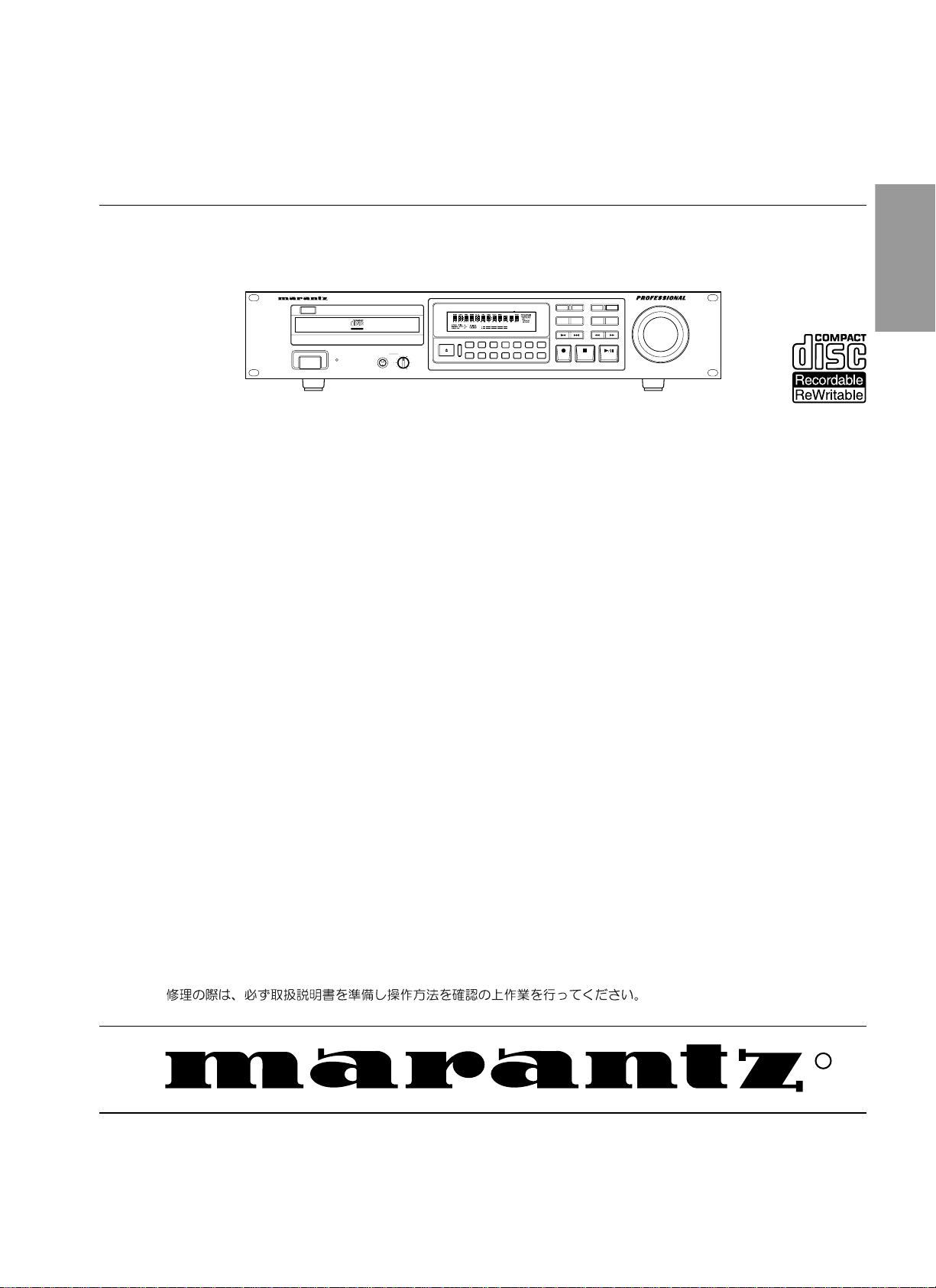
POWER
CD Recorder
CD RECORDER CDR631
IR
Recordable
ReWritable
STANDBY
HEADPHONE LEVEL
010
TIME
TEXT
12
6
4
3
9
8
7
TR.INCR.
REC MODE
FINAL
PROG
5
INPUT
0
REPEATRANDOM
STORE
DELETE
MENU
CANCL
ERASE
REC LEVEL/SELECT
PUSH ENTER
CDR631
TABLE OF CONTENTS
SECTION PAGE
MAIN UNIT
1. Servicing the CDR631 ............................................................................................................................... 1
2. TECHNICAL SPECIFICATIONS ............................................................................................................... 3
3. WARNINGS .............................................................................................................................................. 4
4. SERVICE HINTS AND TOOLS ................................................................................................................. 5
5. DIAGNOSTIC SOFTWARE ....................................................................................................................... 6
6. FAULTFINDING TREES ......................................................................................................................... 10
7. FAULTFINDING GUIDE .......................................................................................................................... 14
8. WIRING DIAGRAM ................................................................................................................................. 29
9. BLOCK DIAGRAM ................................................................................................................................... 31
10. SCHEMATIC DIAGRAM AND PARTS LOCATION ................................................................................. 33
11. EXPLODED VIEW AND PARTS LIST ..................................................................................................... 43
12. ELECTRICAL PARTS LIST ..................................................................................................................... 46
Please use this service manual with referring to the user guide ( D.F.U. ) without fail.
R
Printed in Japan
CDR631
387K855010 MIT
3120 785 22410
First Issue 2001.02
Page 2
MARANTZ DESIGN AND SERVICE
MARANTZ AMERICA, INC.
Using superior design and selected high grade components, MARANTZ company has created the ultimate in stereo sound.
Only original MARANTZ parts can insure that your MARANTZ product will continue to perform to the specifications for which
it is famous.
Parts for your
MARANTZ equipment are generally available to our National Marantz Subsidiary or Agent.
ORDERING PARTS :
Parts can be ordered either by mail or by Fax.. In both cases, the correct part number has to be specified.
The following information must be supplied to eliminate delays in processing your order :
1. Complete address
2. Complete part numbers and quantities required
3. Description of parts
4. Model number for which part is required
5. Way of shipment
6. Signature : any order form or Fax. must be signed, otherwise such part order will be considered as null and void.
USA
MARANTZ AMERICA, INC
440 MEDINAH ROAD
ROSELLE, ILLINOIS 60172
USA
PHONE : 630 - 307 - 3100
FAX : 630 - 307 - 2687
AMERICAS
SUPERSCOPE TECHNOLOGIES, INC.
MARANTZ PROFESSIONAL PRODUCTS
2640 WHITE OAK CIRCLE, SUITE A
AURORA, ILLINOIS 60504 USA
PHONE : 630 - 820 - 4800
FAX : 630 - 820 - 8103
AUSTRALIA
QualiFi Pty Ltd,
24 LIONEL ROAD,
MT. WAVERLEY VIC 3149
AUSTRALIA
PHONE : +61 - (0)3 - 9543 - 1522
FAX : +61 - (0)3 - 9543 - 3677
NEW ZEALAND
WILDASH AUDIO SYSTEMS NZ
14 MALVERN ROAD MT ALBERT
AUCKLAND NEW ZEALAND
PHONE : +64 - 9 - 8451958
FAX : +64 - 9 - 8463554
EUROPE / TRADING
MARANTZ EUROPE B.V.
P.O.BOX 80002, BUILDING SFF2
5600 JB EINDHOVEN
THE NETHERLANDS
PHONE : +31 - 40 - 2732241
FAX : +31 - 40 - 2735578
AUSTRALIA
TECHNICAL AUDIO GROUP PTY, LTD
558 DARLING STREET,
BALMAIN, NSW 2041,
AUSTRALIA
PHONE : 61 - 2 - 9810 - 5300
FAX : 61 - 2 - 9810 - 5355
THAILAND
MRZ STANDARD CO.,LTD
746 - 754 MAHACHAI ROAD.,
WANGBURAPAPIROM, PHRANAKORN,
BANGKOK, 10200 THAILAND
PHONE : +66 - 2 - 222 9181
FAX : +66 - 2 - 224 6795
TAIWAN
PAI- YUING CO., LTD.
6 TH FL NO, 148 SUNG KIANG ROAD,
TAIPEI, 10429, TAIWAN R.O.C.
PHONE : +886 - 2 - 25221304
FAX : +886 - 2 - 25630415
BRAZIL
PHILIPS DA AMAZONIA IND. ELET. ITDA
CENTRO DE INFORMACOES AO
CEP 04698-970
SAO PAULO, SP, BRAZIL
PHONE : 0800 - 123123
FAX : +55 11 534. 8988
(Discagem Direta Gratuita)
CANADA
LENBROOK INDUSTRIES LIMITED
633 GRANITE COURT,
PICKERING, ONTARIO L1W 3K1
CANADA
PHONE : 905 - 831 - 6333
FAX : 905 - 831 - 6936
SINGAPORE
WO KEE HONG DISTRIBUTION PTE LTD
130 JOO SENG ROAD
#03-02 OLIVINE BUILDING
SINGAPORE 368357
PHONE : +65 858 5535 / +65 381 8621
FAX : +65 858 6078
MALAYSIA
WO KEE HONG ELECTRONICS SDN. BHD.
SUITE 8.1, LEVEL 8, MENARA GENESIS,
NO. 33, JALAN SULTAN ISMAIL,
50250 KUALA LUMPUR, MALAYSIA
PHONE : +60 3 - 2457677
FAX : +60 3 - 2458180
JAPAN
MARANTZ JAPAN, INC.
Technical
35- 1, 7- CHOME, SAGAMIONO
SAGAMIHARA - SHI, KANAGAWA
JAPAN 228-8505
PHONE : +81 42 748 1013
FAX : +81 42 741 9190
KOREA
MK ENTERPRISES LTD.
ROOM 604/605, ELECTRO-OFFICETEL, 16-58,
3GA, HANGANG-RO, YONGSAN-KU, SEOUL
KOREA
PHONE : +822 - 3232 - 155
FAX : +822 - 3232 - 154
SHOCK, FIRE HAZARD SERVICE TEST :
CAUTION : After servicing this appliance and prior to returning to customer, measure the resistance between either primary AC
cord connector pins ( with unit NOT connected to AC mains and its Power switch ON ), and the face or Front Panel of product and
controls and chassis bottom.
Any resistance measurement less than 1 Megohms should cause unit to be repaired or corrected before AC power is applied, and
verified before it is return to the user/customer.
Ref. UL Standard No. 813.
In case of difficulties, do not hesitate to contact the Technical
Department at above mentioned address.
001120MIT
Page 3
1.Servicing the CDR631
1.1 INTRODUCTION:
The CDR631is the professional version of a CD recorder, this means that the SCMS (Serial Copy Management System) is
not included. The CDR631can record on the Audio and CDRs PC.
The CDR631is suitable for recording and playback of CD-R W discs (CD-Re Writable disc).
Playback & Recording and Disc
Disc
Player/Recorder
Audio CD Player
Current products Ex:CD-17
Audio CD Player
CD-RW playback Ex:CD-17MK II
CD-RW Recorder
For Professional Ex:CDR630/631/640
CD-RW Recorder
For Consumer Ex:DR6000/6050
CDR
CD
Consumer Disc
Finalized
non
Finalized
Professional Disc
Finalized Finalized
non
Finalized
Consumer Disc
Finalized
PP no P no no no no no -
PP no P no P no P no -
P P P/R P P/R P/R P/R P/R P/R no
P P P/R PPPP P/R P/R YES
CD-RW
non
Finalized
Professional Disc
non
Finalized
SCMS
Consumer : For Digital Audio
Professional : For General use (Including PC)
P : Playback
R : Recording
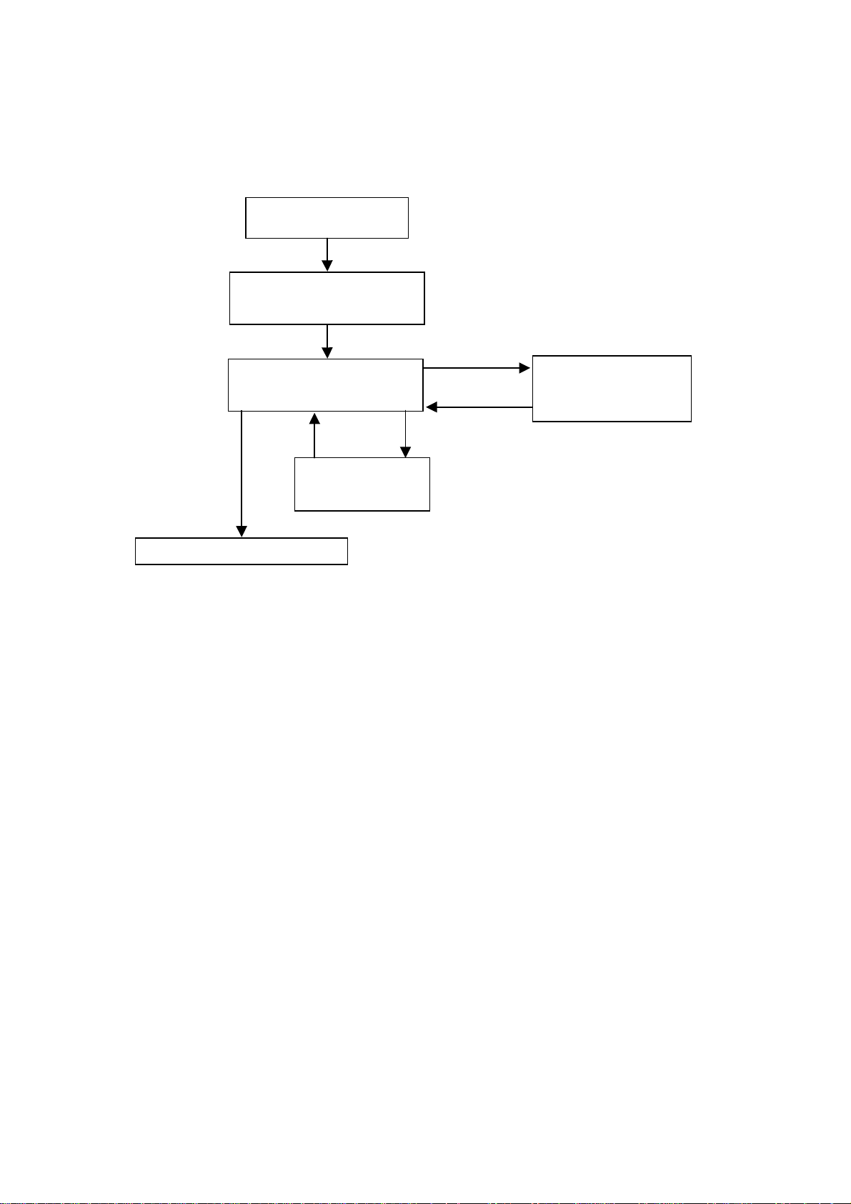
1.2 OPENING THE PRODUCT:
The product can be opened by removing the top cover (8 screws). Once the product is opened one can have access to the
several PCB's and the main module. To have access to the Display PCB, the Headphone PCB first the front cover has to
be removed.
SWITCHING POWER
SUPPLY BOARD
MOTER
BOARD
CDR LOADER
DISPLAY BOARD
Below the several PCB's and it function and service policy will be discussed:
AUDIO
BOARD
HEAD
PHONE
BOARD
1
Page 4

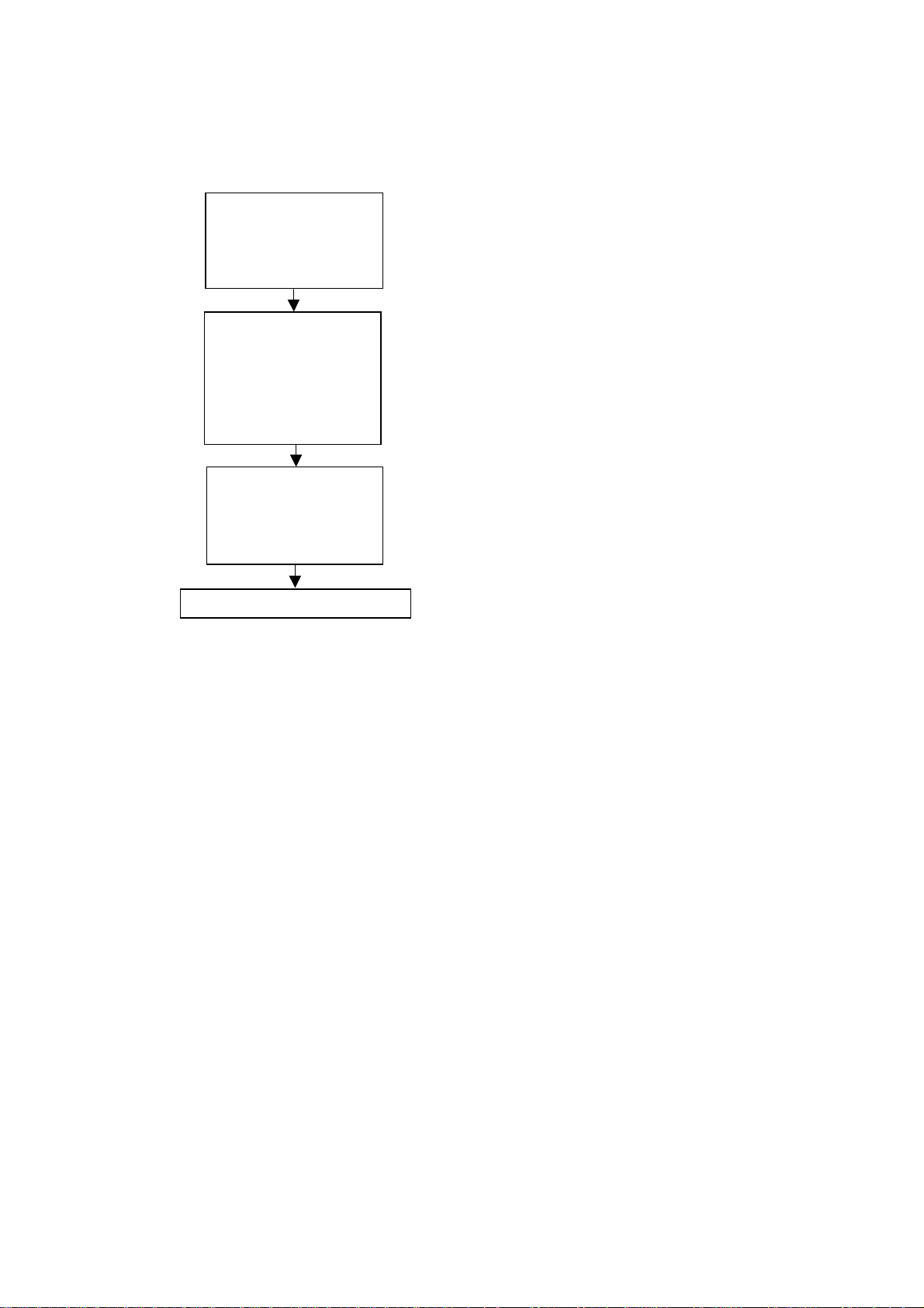
1.2.1 CDR loader (CDR main module CDL4009 or MAR770):
This complete CDR loader is considered as not repairable in the field. therefore this module will be repaired centrally. A
module exchange procedure will be set up for this purpose. The module can be removed from the product by removing 4
screws and the transformer (see demounting the CDR module on page 1-7), and loosing the connectors.
This module is the complete CD recorder, it contains the following parts:
CD Mechanism (CDM4009'). Underneath this mechanism a PCB is mounted which is adjusted to the mechanism (laser
current settings are stored in EEPROM).
Loader Assy. This mechanical assy takes care for the tray control.
Main PCB. This PCB takes care that the (analog or digital) signal to be recorded is converted into a suitable signal which
can be recorded on the disc.
Digital signals with an other sampling frequency then 44.1kHz will be converted in the sample rate converter (DASP) to
44.1kHz.
Analog signals will be first converted into a digital converter by the AD converter.
This PCB also takes care that the signal from the CD (playback) is converted into a suitable digital signal (or analog via
the DA converter).
The main microprocessor controls the several functions of this PCB.
1.2.2 Switching Power Supply Board.
This PCB contains the Power Supply, which delivers the sevelal volteges for the each PCB in the CDR631. On this Power
Supply a fuse (Primaly side) are mounted on this PCB. The power SW is jointed the Power bottom on the front panel.
All parts are available as spare parts.
1.2.3 Audio Board.
This PCB contains the audio part,witch takes care that the signal from CDR main module is converted into an analog signal
via DA converter and outputs the analog signal. This PCB contains the output and input connectors also. All parts are available
as spare parts.
1.2.4 Display Board.
This PCB contains the Display, which informs the user about the status of the recording/playback process and it also takes
care for scanning the keys on the front panel. The information from the keys is fed via a I C connection to the main
microprocessor on the CDR loader module. Information which needs to be displayed is also fed via this I C line from the
main microprocessor on the CDR loader module to the display controller.
The parts for this PCB are available as service parts so this PCB can be repairable up to component level.
2
2
1.2.5 Headphone Board.
This PCB contains the headphone socket and potentiometer which controls the headphone volume. All parts are available
as spare parts.
IMPORTANT
In case of replace the CD-R module "MAR770", the initialization is necessary.
Please initialize the CD-R module with following orders.
1. Press the POWER button (POWER ON) while depressing FINALIZE button and REC
MODE button together.
2. FL Display shows;
WAIT
PGM PROTOCOL
PGM PORT END
3. Press the POWER button (POWER OFF).
Then the CD-R module set up to CDR631 own status.
2
Page 5

2 TECHNICAL SPECIFICATIONS
GENERAL
System .................................................................................................... Compact disc digital audio
Number of channels ................................................................................ 2 (stereo)
Applicable discs ...................................................................................... CD, CD-R , CD-RW
Power Requirement
F version ........................................................................................... AC 100 V 50 / 60 Hz
N version ........................................................................................... AC 100 - 240 V 50 /60 Hz
U version. .......................................................................................... AC 120 V 60 Hz
Power Consumption ................................................................................ 19 W
Operating Temperature . ......................................................................... 5 °
Dimension (MAX)
Width ................................................................................................. 483 mm
Height ................................................................................................ 100 mm
Depth ................................................................................................ 340 mm
Weight ................................................................................................ 4.7 kg
AUDIO
Frequency Response ............................................................................. 20 Hz - 20 kHz
Playback S/N .......................................................................................... 108 dB
Playback Dynamic Range ....................................................................... 95 dB
Playback Total Harmonic Distortion ........................................................ 92 dB
Recording S/N (analog) .......................................................................... 96 dB
Recording Dynamic Range (analog) ....................................................... 92 dB
Recording Total Harmonic Distortion (analog) ........................................ 88 dB
Analog Output Voltage ............................................................................. 2 Vrms
Digital Coaxial Output ............................................................................. 0.5 V (p-p) / 75 ohms
Digital Optical Output .............................................................................. - 20 dB
Headphones ............................................................................................ 0 - 5 Vrms / 8 - 2000 ohms
Recording values for line input
Digital Coaxial Input (automatic sample rate conversion) ....................... 11 - 56 kHz
Digital Optical Input (automatic sample rate conversion) ........................ 11 - 56 kHz
Digital XLR Input (automatic sample rate conversion) ............................ 11 - 56 kHz
Analog Input Sensitivity (Unbalanced) .................................................... 500 mVrms / 50 kohms
Analog Input Sensitivity (Balanced) ........................................................ 0 dBu to +22 dBu / 50 kohms
(default setting : +16 dBu / 50 kohms)
Specifications subject to change without prior notice.
C - 35 °C
3
Page 6
3. WARNINGS
WARNING
All ICs and many other semiconductors are susceptible to
electrostatic discharges (ESD). Careless handling during
repair can reduce life drastically.
When repairing, make sure that you are connected with the
same potential as the mass of the set via a wristband with
resistance. Keep components and tools at this potential.
ATTENTION
Tous les IC et beaucoup d´autres semi-conducteurs sont
sensibles aux décharges statiques (ESD). Leur longévite
pourrait être considérablement écourtée par le fait qu´aucune
précaution nést prise à leur manipulation.
Lors de réparations, s´assurer de bien être relié au même
potentiel que la masse de l´appareil et enfileer le bracelet
serti d´une résistance de sécurité.
Veiller à ce que les composants ainsi que les outils que l´on
utilise soient également à ce potentiel.
WARNUNG
Alle ICs und viele andere Halbleiter sind empfindlich
gegenüber elektrostatischen Entladungen (ESD).
Unsorgfältige Behandlung im Reparaturfall kann die
Lebensdauer drastisch reduzieren.
Sorgen Sie dafür, daß sie im Reparaturfall über ein Pulsarmband mit Widerstand mit dem Massepotential des
Gerätes verbunden sind.
Halten Sie Bauteile und Hilfsmittel ebenfalls auf diesem
Potential.
AVAILABLE ESD PROTECTION EQUIPMENT :
anti-static table mat large 1200x650x1.25mm 4822 466 10953
anti-static wristband 4822 395 10223
connection box (3 press stud connections, 1M ) 4822 320 11307
extendible cable (2m, 2M , to connect wristband to connection box) 4822 320 11305
connecting cable (3m, 2M , to connect table mat to connection box) 4822 320 11306
earth cable (1M , to connect any product to mat or to connection box) 4822 320 11308
KIT ESD3 (combining all 6 prior products - small table mat) 4822 310 10671
wristband tester 4822 344 13999
ESD
WAARSCHUWING
Alle IC´s en vele andere halfgeleiders zijn gevoelig voor
electrostatische ontladingen (ESD).
Onzorgvuldig behandelen tijdens reparatie kan de levensduur
drastisch doen vermindern. Zorg ervoor dat u tijdens reparatie
via een polsband met weerstand verbonden bent met hetzelfde
potentiaal als de massa van het apparaat.
Houd componenten en hulpmiddelen ook op ditzelfde potentiaal.
AVVERTIMENTO
Tutti IC e parecchi semi-conduttori sono sensibili alle scariche
statiche (ESD).
La loro longevità potrebbe essere fortemente ridatta in caso di
non osservazione della più grande cauzione alla loro
manipolazione. Durante le riparationi occorre quindi essere
collegato allo stesso potenziale che quello della massa
delápparecchio tramite un braccialetto a resistenza.
Assicurarsi che i componenti e anche gli utensili con quali si
lavora siano anche a questo potenziale.
small 600x650x1.25mm 4822 466 10958
Safety regulations require that the set be restored to its
original condition and that parts which are identical with
those specified be used.
Safety components are marked by the symbol
Les normes de sécurité exigent que l`appareil soit remis
à l`état d`origine et que soient utilisées les pièces de
rechange identiques à celles spécifiées.
Les composants de sécurité sont marqués
Bei jeder Reparatur sind die geltenden Sicherheitsvorschriften zu beachten. Der Originalzustand des Gerätes
darf nicht verändert werden. Für Reparaturen sind Originalersatzteile zu verwenden.
Sicherheitsbauteile sind durch das Symbol markiert.
U : VERSION N : VERSION
DANGER: Invisible laser radiation when open.
AVOID DIRECT EXPOSURE TO BEAM.
Varning !
Advarsel !
Osynlig laserstrålning när apparaten är öppnad och
spärren är urkopplad. Betrakta ej strålen.
Usynlig laserstråling ved åbning når sikkerhedsafbrydere
er ude af funktion. Undgå udsaettelse for stråling.
CLASS III b
LASER PRODUCT
SAFETY
Veiligheidsbepalingen vereisen, dat het apparaat in zijn
oorspronkeliijke toestand wordt teruggebracht en dat
onderdelen, identiek aan de gespecificeerde, worden toegepast.
De Veiligheidsonderdelen zijn aangeduid met het symbool
Le norme di sicurezza estigono che l´apparecchio venga
rimesso nelle condizioni originali e che siano utilizzati i
pezzi di ricambiago identici a quelli specificati.
Componenty di sicurezza sono marcati con
CLASS 3B
LASER PRODUCT
Varoitus !
Avatussa laitteessa ja suojalukituksen ohitettaessa olet alttiina
näkymättömälle laserisäteilylle. Älä katso säteeseen !
After servicing and before returning the set to customer
perform a leakage current measurement test from all
exposed metal parts to earth ground, to assure no
shock hazard exists.
The leakage current must not exceed 0.5mA.
"Pour votre sécurite, ces documents doivent être utilisés par
des spécialistes agréés, seuls habilités à réparer votre
appareil en panne".
4
Page 7

4. SERVICE HINTS AND TOOLS
SERVICE TOOLS
“The tools listed below are standard test tools that can be used for repairing and testing Marantz
CD Players & Recorders. Unless otherwise stated in the text, these tools are not mandatory for
servicing Marantz CD Players & Recorders”
Audio signals disc 4822 397 30184
Disc without errors (SBC444)+
Disc with DO errors, black spots and fingerprints (SBC444A) 4822 397 30245
Disc (65 min 1kHz) without no pause 4822 397 30155
Max. diameter disc (58.0 mm) 4822 397 60141
Torx screwdrivers
Set (straight) 4822 395 50145
Set (square) 4822 395 50132
13th order filter 4822 395 30204
Hexagon socket screw button (No. 1.5)
5
Page 8

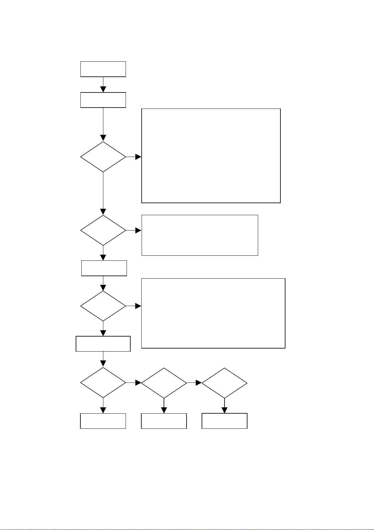
5. Diagnostic Software
5.1 Electrical service diagnostics
ELECTRICAL SERVICE DIAGNOSTICS
(software versions, test for defective components)
If power ON,
switch power OFF
Load CD-DA disc (SBC444A)
Press <PLAY> + <F FWD>
simultaneously and switch ON unit
PLAYER
INFORMATION
Display :
"PLAYER ID"
"SW VERSION BACK END"
"SW VERSION CDR LOADER"
(DR6050
CDR MAIN
BOARD TEST
Display :
PASS OR FAIL
Display :
PASS OR FAIL
Display :
PASS OR FAIL
Display :
PASS OR FAIL
Display :
PASS OR FAIL
Display :
PASS OR FAIL
"SW VERSION CD LOADER"
"DTST1"
DRAM test (7702)
"DTST2"
FLASH CHECKSUM test (7702)
"DTST3"
FLASH ERASE test (7702)
"DTST4" *
CODEC test (7702)
"DTST5"
CDR LOADER
COMMUNICATION test
"DTST5"
*
CD LOADER
COMMUNICATION test
* FOR CDR500 ONLY
)
ABORT TEST
Press <F FWD>
ABORT TEST
Press <F FWD>
ABORT TEST
Press <F FWD>
ABORT TEST
Press <F FWD>
ABORT TEST
Press <F FWD>
ABORT TEST
Press <F FWD>
ABORT TEST
Press <F FWD>
LOADER TESTS
CDR LOADER TEST
CD-DA disc must be loaded
Display shows current disc time
Test OK?
YES
CD LOADER TEST *
CD-DA disc must be loaded
Display shows current disc time
Test OK?
YES
DISPLAY TEST
DISPLAY TEST
Display segments blink at f=1Hz
KEYBOARD &
RC TEST
KEYBOARD & RC TEST
Display shows name of pressed keys
Press <F FWD>
NO
Display :
or
or
* FOR CDR500 ONLY
NO
Display :
or
or
"BERR1"
"NO CDDA"
"NO DISC"
Press <F FWD>
"BERR2"
"NO CDDA"
"NO DISC"
Press <F FWD>
Tests OK?
YES
NO
Display :
n = failed test
Display next
failed test
To end test, switch OFF unit
"DERRn"
Figure 5-1
6
Page 9

5.1.1 Description
The intention of the electrical service diagnostics is to show the
software versions present in the player and to direct the dealer
towards defective internal units. The units are : the CDR main
board, the CDR loader, the CD loader in case of a CDR500 and
the keyboard/display board. A sequence of tests is executed
automatically. Some of the tests can be aborted or skipped
without the result being taken into account. External tools or
disassembly of the unit is not necessary to get the diagnostic
information. Pressing keys [PLAY/PAUSE] and [F FWD]
simultaneously while switching on the unit, starts the test.
Switching off the unit ends the test.
5.1.2 Requirements to perform the test
• Working keyboard to start up the test.
• Working local display to check the output messages.
• A CD-DA disc with a minimum of 3 tracks in all trays to
perform the disc test.
5.1.3 Description of the tests
Player information
In this part of the test the following important information can be
checked without removing the cover :
• Recorder ID.
• SW-version back end of player.
• SW-version CDR loader.
• SW-version CD loader (only for CDR500).
CDR main board test
As soon as the CDR main board tests are finished, all failure
messages (if any) will be displayed sequentially by pressing the
[F FWD] key. The message "DERRn" will be displayed with n
indicating the faulty test number.
If one of the tests is aborted with the [F FWD] key, no error
message will be displayed for this test. The flash data erase
test ("DTST3") can not be aborted !
The CDR main board test consists out of :
DRAM test
Display : "DTST1". The DRAM used for buffer management is
tested by writing, reading and verifying test patterns.
Flash checksum test
Display : "DTST2". This test checks the checksum of the
player's SW stored in the flash.
Flash data erase
Display : "DTST3". During this test, all temporary information
(CDtxt) in the flash is erased.
CODEC (ADC/DAC) test
Display : "DTST4". This test checks the CODEC IC by writing,
reading and verifying test patterns. The test is not applicable for
CDR950.
CDR communication test
Display : "DTST5". The communication between the host
processor (DASP) and the CDR loader via the DSA-R-bus is
tested.
CD communication test
Display : "DTST6"). The communication between the host
processor (DASP) and the CD loader is tested. The test is only
applicable for CDR500.
Loader tests
These tests determine if the CDR loader and the CD loader in
case of a CDR500 work correctly. A CD-DA disc with a
minimum of 3 tracks needs to be inserted in both loaders. A
disc test is executed to check focus control, disc motor control,
radial control and jump grooves control. The disc test is
performed by audio play-back of 5 seconds at the beginning,
middle and end of the disc.
CDR loader test
During the test, the current disc time is shown. In case of an
error the message "BERR1" will be displayed and the [F FWD]
key must be pressed to continue with the following test.
Pressing the [F FWD] key also aborts this test.
CD loader test
For CDR500 only. During the test, the current disc time is
shown. In case of an error the message "BERR2" will be
displayed and the [F FWD] key must be pressed to continue
with the following test. Pressing the [F FWD] key also aborts
this test.
Display test
All segments will blink at a frequency of 1 Hz. Pressing the [F
FWD] key will start the next test because the user has to check
for himself if all segments work properly.
Keyboard and remote control tests
The test will give the user the ability to test every key without
executing the function assigned to it. Therefore, the user needs
to press every key on the keyboard and the remote control. The
display will show the name of the key being pressed. Pressing
more than one key at once will give an unpredictable result
except for the service combinations : [PLAY/PAUSE] + [STOP],
[PLAY/PAUSE] + [ERASE] + [RECORD], [PLAY/PAUSE] +
[RECORD].
7
Page 10
5.2 Mechanical service diagnostics
MECHANICAL SERVICE DIAGNOSTICS
(test for defective components)
If power ON,
switch power OFF
Press <PLAY/PAUSE> + <STOP>
simultaneously and switch
To end test, switch OFF unit
ON unit
FOCUS TEST
Display shows
Visual inspection
SLEDGE TEST
Visual inspection
Display shows
“BUSY”
“BUSY”
<
OPEN
>
<
CLOSE
>
<FWD><REWIND>
TRAY TEST
Visual inspection
Display shows
even if tray is blocked
“OPENED”
5.2.1 Description
No external tools are required to perform this test. The cover
needs to be removed because the user has to check the
movements of the tray, focus and sledge visually. Pressing
keys [PLAY/PAUSE] and [STOP] simultaneously while
switching on the unit, starts the test. Switching off the unit ends
the test. In case of a CDR500, one can check the CD loader
mechanics in the same way by pressing the above key
combination on the CD player keys.
5.2.2 Requirements to perform the test
• Working keyboard to cycle through the tests and to start up
the test.
• Working local display to check the output messages.
5.2.3 Description of the tests
Focus control test
The focussing lens is continuously moving up and down. The
display reads "BUSY".
Sledge control test
After pressing [F FWD] the sledge continuously moves up and
down. Pressing [REWIND] stops the sledge at the position it is
in and the focus control test resumes. The display reads
"BUSY".
Figure 5-2
pressing [F FWD]. One has to stop these tests pressing
[REWIND] before it is possible to close the tray again.
Depending on the action the display reads "OPEN",
"OPENED", "CLOSE" or "BUSY".
Tray control test
This test starts from within the focus control test routine.
Pressing [OPEN/CLOSE] moves the tray in or out. In the tray
open position one can initiate focus and sledge tests by
8
Page 11
5.3 DC-erase service mode
DC ERASE SERVICE MODE
(erasement of complete CD-RW)
Load CD-RW disc
<ERASE> + <RECORD>
simultaneously and switch
Display shows:
“
ER mm:ss
Press
ON unit
”
mm
ss :remaining seconds
TOTAL
illuminated
To end test, switch OFF unit
:remaining minutes
and
REM
are also
Display shows:
“
when the erase function is
PASSED
completed
ERROR
“
if DC ERASE fails
Figure 5-3
”
”
5.3.1 Description
This test is initiated by pressing [ERASE] and [RECORD]
simultaneously while switching on the unit. The player will
erase a complete CD-RW disc (including PMA and ATIP lead
out area) at speed N=2. The display shows the countdown of
the remaining time required for the operation to complete. The
format is "ER mm:ss", where "mm" are the remaining minutes
and "ss" the remaining seconds. After completion the message
"PASSED" is shown, and the player has to be switched off and
on again to start up in normal operating mode. Switching off the
unit before completion of the test, leaves the disc in an
unpredictable state. In such case only a complete DC-erase
procedure can recover the CD-RW disc.
5.3.2 Requirements to perform the test
• Functional CDR player.
• A CD-RW audio disc must be present in the tray.
9
Page 12
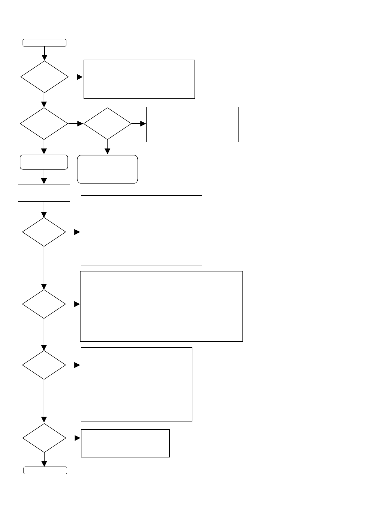
6. Faultfinding Trees
NO DISC LOADED
SWITCH ON POWER
PRESS <DISPLAY>
DISPLAY?
YES
DISPLAY:
"INSERT DISC"
YES
CHECK:
• MAINS, MAINS CABLE
• POWER SUPPLY & TRAFO
⇒
WIRING
⇒
ON/OFF SWITCH
⇒
FUSES
⇒
NO
• DISPLAY (SEE FAULT FINDING GUIDE DISPLAY BOARD)
CHECK:
NO
• WIRING
• POWER SUPPLY VOLTAGES
• ELECTRICAL SERVICE DIAGNOSTICS:
REPLACE CDR MODULE IF
OR
VOLTAGES
⇒
WIRING
⇒
SUPPLY VOLTAGES
⇒
CLOCK SIGNAL 8MHz
⇒
CONTROL SIGNALS
⇒
KEYBOARD
⇒
STANDBY LED
⇒
ELECTRICAL SERVICE DIAGNOSTICS:
DISPLAY TEST, KEYBOARD TEST
"DERRn"
"BERRn"
ERROR OCCURS
PRESS
<OPEN/CLOSE>
TRAY?
YES
INSERT DISC
PRESS <OPEN/CLOSE>
CD-DA DISC
LOADED?
SEE CD-DA DISC
FAULT FINDING
CHECK:
• DISPLAY BOARD (SEE FAULT FINDING GUIDE DISPLAY BOARD)
⇒
NO
• MECHANICAL SERVICE DIAGNOSTICS:
REPLACE CDR MODULE IF ERROR OCCURS
YESYES
SEE CD-R DISC
FAULT FINDING
WIRING
⇒
SUPPLY VOLTAGES
⇒
CLOCK SIGNAL 8MHz
⇒
CONTROL SIGNALS
⇒
KEYBOARD
⇒
ELECTRICAL SERVICE DIAGNOSTICS:
DISPLAY TEST, KEYBOARD TEST
CD-R DISC
LOADED?
NONO
SEE CD-RW DISC
CD-RW DISC
LOADED?
YES
FAULT FINDING
Figure 6-1
10
Page 13
Faultfinding T rees
CD-DA DISC LOADED
DISC
DETECTION &
READING?
YES
DISPLAY:
“CD”
&
T.O.C. INFO?
YES
PRESS <PLAY>
NO
NO
CHECK:
• WIRING
• POWER SUPPLY VOLTAGES
• ELECTRICAL SERVICE DIAGNOSTICS:
REPLACE CDR MODULE IF
OR
"BERRn"
CHECK:
• DISC: DIRT, SCRATCHES, DAMAGED...
• ELECTRICAL SERVICE DIAGNOSTICS:
REPLACE CDR MODULE IF
OR
"BERRn"
ERROR OCCURS
ERROR OCCURS
"DERRn"
"DERRn"
ANALOG
AUDIO
OUT?
YES
DISTORTION?
NO
HEADPHONE?
YES
DIGITAL
AUDIO
OUT?
YES
PLAY BACK OF CD-DA
DISCS OK
NO
YES
NO
NO
CHECK:
AUDIO CONNECTIONS & CABLES
•
AUDIO BOARD
•
⇒
FLEX & WIRE CONNECTIONS
⇒
+5V (pin 4. W855), +12V(pin 2. W855), -12V(pin 6. W855)
⇒
SEE FAULTFINDING GUIDE AUDIO BOARD - ANALOG OUT PATH
• ELECTRICAL SERVICE DIAGNOSTICS:
REPLACE CDR MODULE IF
OR
"BERRn"
CHECK:
CONNECTION OF HEADPHONE
•
HEADPHONE BOARD
•
⇒
⇒
⇒
⇒
⇒
•
ELECTRICAL SERVICE DIAGNOSTICS:
REPLACE CDR MODULE IF
OR
"BERRn"
CHECK:
AUDIO CONNECTIONS & CABLES
•
AUDIO BOARD
•
⇒
⇒
⇒
• ELECTRICAL SERVICE DIAGNOSTICS:
REPLACE CDR MODULE IF
OR
"BERRn"
ERROR OCCURS
WIRE CONNECTION
+10V (pin 6. J903), -10V (pin 2. J903)
KILL VOLTAGE (pin 1. J903) : -8V DURING PLAY
KILL TRANSISTORS QN01 - QN02
PLAY SBC442 DISC (1kHz, -30dB) AND CHECK SIGNAL AT
Q901
ERROR OCCURS
FLEX & WIRE CONNECTIONS
+5V (pin 3. W853)
CHECK SINGNAL
-FOR COAXIAL OUT AT QT31,LT13
-FOR OPTICAL OUT AT QT31,JT21
ERROR OCCURS
"DERRn"
"DERRn"
"DERRn"
Figure 6-2
11
Page 14
CD-R DISC LOADED
DISC
DETECTION &
READING?
YES
DISPLAY:
“CD R”
&
OPC INFO?
YES
NO
NO
CHECK:
• WIRING
• POWER SUPPLY VOLTAGES
• ELECTRICAL SERVICE DIAGNOSTICS:
REPLACE CDR MODULE IF
OR
"BERRn"
DISPLAY:
“CD”
OR
T.O.C. INFO?
YES
ERROR OCCURS
“CD R”
&
NO
"DERRn"
CHECK:
• DISC: DIRT, SCRATCHES, DAMAGED...
• ELECTRICAL SERVICE DIAGNOSTICS:
REPLACE CDR MODULE IF
OR
"BERRn"
ERROR OCCURS
"DERRn"
CD-R DISC EMPTY
START MANUAL
RECORDING FROM
ANALOG SOURCE
ANALOG IN?
YES
LEVEL
ADJUSTABLE?
YES
FINALISED OR PARTIALLY
RECORDED CD-R DISC
LOADED :
SEE CD-DA DISC
FAULT FINDING
CHECK:
AUDIO CONNECTIONS & CABLES
•
AUDIO BOARD
•
⇒
+10V (QM01), -10V (QM02)
⇒
NO
CHECK SINGNAL
-FOR BALANCE IN AT Q326
-FOR UNBALANCE IN AT Q331
-FOR BALANCE & UNBALANCE IN AT Q332
-FOR OPTICAL IN AT J301
• ELECTRICAL SERVICE DIAGNOSTICS:
REPLACE CDR MODULE IF
OR
"BERRn"
CHECK:
AUDIO CONNECTIONS & CABLES
•
DISPLAY BOARD (SEE FAULT FINDING GUIDE DISPLAY BOARD)
•
NO
AUDIO
•
• ELECTRICAL SERVICE DIAGNOSTICS:
REPLACE CDR MODULE IF
OR
"BERRn"
ERROR OCCURS
⇒
EASY JOG KNOB
⇒
I2C COMMUNICATION
⇒
ELECTRICAL SERVICE DIAGNOSTICS:
KEYBOARD TEST
BOARD (SEE FAULT FINDING GUIDE I/O BOARD - ANALOG IN PATH)
ERROR OCCURS
"DERRn"
"DERRn"
DIGITAL IN?
OPTICAL IN?
YES
RECORDING
SUCCESSFUL?
YES
SET OK
CHECK:
AUDIO CONNECTIONS & CABLES
•
NO
AUDIO BOARD
•
⇒
⇒
⇒
FLEX AND WIRE CONNECTIONS
+5V (pin 3 conn. W853)
CHECK SINGNAL
-FOR XLR IN AT Q326
-FOR COAXIAL IN AT Q331
-FOR XLR & COAXIAL IN AT Q332
-FOR OPTICAL IN AT J301
• ELECTRICAL SERVICE DIAGNOSTICS:
REPLACE CDR MODULE IF
OR
"BERRn"
NO
CHECK:
• ELECTRICAL SERVICE DIAGNOSTICS:
REPLACE CDR MODULE IF
OR
"BERRn"
ERROR OCCURS
ERROR OCCURS
Figure 6-3
"DERRn"
"DERRn"
12
Page 15

CD-RW DISC LOADED
DISC
DETECTION &
READING?
YES
DISPLAY:
“CD RW”
OPC INFO?
YES
&
NO
NO
CHECK:
• WIRING
• POWER SUPPLY VOLTAGES
• ELECTRICAL SERVICE DIAGNOSTICS:
REPLACE CDR MODULE IF
OR
DISPLAY:
“CD”
OR
T.O.C. INFO?
YES
"BERRn"
ERROR OCCURS
“CD RW”
&
"DERRn"
CHECK:
NO
• DISC: DIRT, SCRATCHES, DAMAGED...
• ELECTRICAL SERVICE DIAGNOSTICS:
REPLACE CDR MODULE IF
OR
"BERRn"
ERROR OCCURS
"DERRn"
CD-RW DISC EMPTY
START ERASING OF LAST RECORDED TRACK
ERASING
SUCCESSFUL?
YES
SET OK
FINALISED OR PARTIALLY
RECORDED CD-RW DISC
NO
CHECK:
• ELECTRICAL SERVICE DIAGNOSTICS:
•
Figure 6-4
LOADED :
SEE CD-DA DISC
FAULT FINDING
REPLACE CDR MODULE IF
OR
"BERRn"
IF DISC CORRUPTED TRY DC ERASE
ERROR OCCURS
"DERRn"
13
Page 16

7. Faultfinding Guide
7.1 Display Board
7.1.1 Description of display board
General description
The display board has three major parts : the FTD (Fluorescent
Tube Display), the display controller TMP87CH74F and the
keyboard. The display controller is controlled by the DASP
master processor on the CDR main board. The communication
protocol used is I2C. So all the information between DASP and
display controller goes via the SDA or I2C DATA and SCL or
I2C CLK lines. Communication is always initiated by the DASP
on the CDR main board. Unlike the previous generations of
CDR players, the interrupt generated by the display controller
at key-press or reception of remote control is not used. Instead,
the DASP polls the display controller for these events.
BLOCK DIAGRAM
TMP87C874F
64 63 62 61 60 59 58 57 56 55254 53
I/O PORT8 (VFT)
65
66
67
68
69
70
71
72
73
74
75
76
77
78
79
80
I/O PORTD (VFT) I/O PORT9 (VFT)
VKK
I/O PORT0
3
1
DATA MEMORY
( RAM )
512X8 BIT
16 BIT
TIMER/COUNTER
8 BIT A/D
CONVERT.
79819
651516
I/O PORT7 (VFT)
PROGR MEMORY
( ROM )
8kX8 BIT
C P U
INTERRUPT
CONTROLLER
CLOCK/TIMING CONTROLLER
( I/O PORT2 )
VSS1
RESETN
XOUT
XIN
P22
P21
10
Display controller TMP87CH74F
TMP87CH74F (QY01) is a high speed and high performance
8-bit single chip microprocessor, containing 8-bit A/D
conversion inputs and a VFT (Vacuum Fluorescent Tube)
driver.
In this application, its functions are :
• slave microprocessor.
• FTD driver.
• generates the square wave for the filament voltage
required for an AC FTD.
• generates the grid and segment scanning for the FTD.
• generates the scanning grid for the key matrix.
• input for remote control.
All the communication runs via the serial bus interface I2C. The
display controller uses an 8Mhz resonator as clock driver.
52
I/O PORT6 (VFT)
PROGRAM
COUNTER
8 BIT
TIMER/COUNTER
I/O PORT1
TEST1
P20
INT0
INT1
13
141211 17 18 20 21 22
41
42434445464748495051
VDD
VAREF
VASS
I C
PORT3
SCL
23 244
I/O PORT5
I/O PORT4
2
SDA
40
39
38
37
36
35
34
33
32
31
30
29
28
27
26
25
SCK0
PIN DESCRIPTIONS
INT0 external interrupt input 0
INT1 external interrupt input 1
RESETN reset signal input, active low
SCL I2C-bus serial clock input/output
SDA I2C-bus serial data input/output
TEST test pin, tied to low
VAREF analog reference voltage input
VASS analog reference ground
VDD +5V
VKK VFT driver power supply
VSS ground
XIN, XOUT resonator connecting pins for high-frequency clock
Figure 7-1
14
Page 17

7.1.2 Test instructions
Supply voltages
The display board receives several voltages via connector
JY01.
• VFTD : -34V ±5% measured at pin 2 of conn. JY52.
• VDC1-VDC2 : 4V1 ±10% measured between pin 1 and 3 of
conn. JY52.
• +5V : + 5V ±5% measured at pin 10 of conn. JY52.
Voltages VFTD, VDC1 and VDC2 are produced in the Switching
Power Supply Board and sent to the display board via the CDR
main board. The +5V voltage is produced on the CDR main
board as D5V.
Clock signal
As clock driver for the display controller, a resonator of 8 Mhz
(XY01) is used. The signal can be measured at pins 8 and 9 of
the display controller : 8 Mhz ±5%.
Grid lines
Level and timing of all grid lines, G1-->G15, can be checked
either at the FTD itself or at the display controller. Grid lines
G13, G14 and G15 each have an extra current amplifier in line
: QY04 for G13, QY03 for G14 and QY02 for G15. A typical
grid line signal shows in the oscillogram below.
PM3392A
+4V
0V
Control signals
RESETN
The reset signal comes via pin 4 of conn. JY52 from the DASP
master processor on the CDR main board (SYS_RESET). The
reset is low active. It should be kept low during power up for at
least 3 machine cycles with supply voltage in operating range
and a stable clock signal (1 machine cycle = 12 x 1/Fc (8 Mhz)
sec.). During normal operation, the reset should be high (3V3).
The high signal is 3V3 because the DASP operates on 3V3.
I2C DATA/I2C CLK
These lines connect to the DASP master processor via
respectively pin 5 and pin 7 of conn. JY52. When there is
no communication, they should have the high level (+5V). The
oscillogram below gives an indication of how these signals
should look like.
PM3392A
+5V
I2C DATA
-34V
CH1!10.0 V= MTB1.00ms ch1+
Figure 7-3 “OSD”
Segment lines
Level and timing of all segment lines, P-->P21, can be
checked either at the FTD itself or atthe display controller.
The data on these segment lines however, depends on the
characters displayed. The oscillogram below shows a
segment line with data. A segment line without data
maintains a -30V level.
PM3392A
+5V
0V
0V
+5V
I2C CLK
0V
CH1!2.00 V=
CH2 2 V= MTB10.0ms ch1+
Figure 7-2 “I2C SIGNALS”
FTD drive lines
Filament voltage
Should measure 4.3V ±10% (=VDC1-VDC2) between pins 1-2
and pins 52-53 of FTD(VY01).
-34V
CH1!10.0 V= MTB1.00ms ch 1+
Figure 7-4 “SEGMENT LINE”
15
Page 18

Key matrix lines
The lines connected to pins 18, 19, 20, 34, 35, 36 and 37 of the
display controller act as matrix scanners. Without a key pressed,
they maintain a low level. As soon as a key is pressed, the
scanning line connected to that key puts out a scanning signal,
which should look like the oscillogram below. This scanning signal
goes via the pressed key to I/O port 7 of the display controller
(pins 28 to 33). The display controller can now determine which
key has been pressed. Without a key pressed, pins 28 to 33 of
the display controller maintain a high level (+5V).
PM3392
Pin1
Pin3
PM3392A
+5V
0V
CH1!2.00 V= MTB5.00ms ch1+
CL 96532121_031.eps
Figure 7-5 KEY MATRIX SCAN LINE
Easy jog knob
Rotary operation
The easy jog knob (SY26) incorporates a whole heap of user
control possibilities in just one knob. Without the knob being
operated, pin 1 and 3 of the knob (and thus pin 16 and 17 of the
display controller), maintain the +5V level. Turning the knob
clockwise briefly connects pin 1 to GND followed by pin 3.
141099
CH1 5.00 V=
CH2 5.00 V= M TB20.0ms- 1.92dv ch2-
CL 96532121_033.eps
141099
Figure 7-7 TURN ANTI-CLOCKWISE
The pulses created this way arrive at pin 16 and 17 of the
display controller. The first pulse to arrive tells the controller the
direction of the rotation. Counting the pulses reveals the
amount of rotation. Combining and decoding this information,
the display controller will execute the appropriate task.
Push button operation
This button connects to the key matrix lines and thus the
operation is identical to the ordinary keys. Without being
pressed, pin 4 of the easy jog maintains the low level, pin 5 the
high level. When pressed the scanning signal goes through the
closed contact of pins 4 and 5, and can be checked at both
pins.
IR receiver - remote control
In the CDR631 the IR receiver ZY01 is mounted on the IR board.
In all versions the IR receiver connects to the display controller.
The signal coming from the receiver can be checked at pin 22 of
the display controller. This signal is normally high (+5V).
When the remote control is being operated, pulses mixed in with
the +5V can be measured. The oscillogram gives an indication of
how the signal looks like with the RC being operated.
PM3392
Pin1
Pin3
CH1 5.00 V=
CH2 5.00 V= MTB20.0ms- 1.92dv ch2-
CL 96532121_032.eps
141099
Figure 7-6 TURN CLOCKWISE
Turning the knob anti-clockwise briefly connects pin 3 to GND
followed by pin 1.
+5V
0V
PM3392A
1
CH1!2.00 V= MTB20.0ms ch1+
CL 96532121_034.eps
Figure 7-8 IR RECEIVER SIGNAL
141099
16
Page 19

7.1.3 Display board troubleshooting guide
SWITCH POWER ON,
EXIT STAND BY
MODE
CHECK :
DISPLAY?
YES
KEY
FUNCTIONS?
YES
NO
NO
• SUPPLY VOLTAGES
⇒ -34V ±5% at conn. JY52-2
⇒ 4V3 ± 10% between conn. JY52-1 and JY52-3
⇒ +5V ± 5 % at conn. JY52-10
• CLOCK SIGNAL
⇒ 8Mhz at pins 8, 9 of QY01
• CONTROL SIGNALS
⇒ RESETN 3V3 (high) at conn.JY52-4 after start up
⇒ I2C DATA at conn. JY52-5
⇒ I2C CLK at conn. JY52-7
• FTD DRIVE LINES
⇒ Filament voltage 4V3 ± 10% between pins 1-2 and
pins 52-53 of the FTD (VY01)
⇒ Grid lines (see test instructions)
⇒ Segment lines (see test instructions)
• ELECTRICAL SERVICE DIAGNOSTICS - Local display test
CHECK:
• KEY MATRIX LINES (see test instructions)
• ELECTRICAL SERVICE DIAGNOSTICS – Keyboard test
• EASY JOG KNOB (see test instructions)
REMOTE
CONTROL?
YES
DISPLAY BOARD
OK
NO
CHECK:
• IR RECEIVER signal at pin 22 of QY01
• ELECTRICAL SERVICE DIAGNOSTICS – Remote control test
Figure 7-9
17
Page 20

7.2 Audio Board
Pin description
The Audio board for the CDR631 is a full high performance
AD/DA panel, acting as an interface to the outside world. Key
components are DS1807, ADC AK5351 and DAC AK4393.
7.2.1 Analog-in path
Description
The via BALANCE in connected anolog-in L and R signals are
pre-amplified by opamp Q761-Q763, and the via UNBALANCE
in connected anolog-in L and R signals are pre-amplified by
opamp Q705, Q706, these signals is selected by Analog SW
Q701 after which they are presented to an adjustable amplifier
made out of DS1807 and opamp Q703 - Q708. The level of the
incoming. Analog signal is adjusted by means of control lines
2
"I
C" coming from the DASP on the CDR main board and
switching the mux/demux. The anolog signal is then presented
to the A/D converter A5351 (QA01) where they are converted
from analog to I
via connector J601 and flex to the DASP on the CDR main
board. The ADC uses the CL11-clock (11.2896 MHz), coming
from the DASP on the CDR main board.
ADC AK5351
Description
The AK5351 is a stereo, 20-bit oversampling ADC based on
Sigma Delta technology intended primarily for digital audio
bandwith applications. It supports the I2S-bus data format. The
device can be used in either slave or master mode. In this
application it is used in slave mode receiving it's clock from the
DASP on the CDR main board.
2
S-bus data format. The I2S-bus is connected
No. Pin Name I/O PIN / FUNCTION
1 AINR+
2 AINR3 VREF
4 VA Analog section Analog Power Supply, +5V
5 AGND Analog section Analog Ground
6 AlNL+
7 AINL-
8 TST1
10 TST2
11 TST3
14 TST4
9 HPFE
12 VD Digital section Digital Power Supply pin, +5V
13 DGND Digital section Digital Ground pin
16 PD
17 MCLK I Master Clock input pin
18 SCLK I/O Serial Data Clock pin
19 LRCK I/O L/R Channel Clock Select pin
20 FSYNC I/O Frame Synchronization Signal pin
21 SDATA O Serial Data Output pin
22 CMODE I Master Clock Selection pin
23 SMODE1 I Serial Interface Mode Select pin
15 SMODE2 I Defines the directions of LRCK, SCLK and FSYNC pins and
24 VB
Right channel analog positive input pin
I
Right channel analog negative input pin
I
Voltage Reference output pin (VA-2.6V)
O
Normally connected to VA with a 0.1uF ceramic capacitor in
parallel with a 10uF electrolytic capacitor.
Left channel analog positive input pin
I
Left channel analog negative input pin
I
Test pin Should be left floating. (Pull- down pin)
Test pin Should be left floating. (Pull- down pin)
Test pin Should be left floating. (Pull- down pin)
Test pin Should be left floating. (Pull- down pin)
High Pass Filter Enable pin (Pull- up pin)
I
"H": ON
"H": OFF
Power Down pin
I
"L" brings the device into power-down mode. Must be done
once after power-on.
CMODE="H" : 384fs
CMODE="L" : 256fs
Data is clocked out at the falling edge of SCLK.
Slave mode: 64fs clock is input usually.
Master mode: SCLK outputs a 64fs clock.
SCLK stays low during the power-down mode(PD="L").
Slave mode: An fs clock is fed to this LRCK pin.
Master mode: LRCK output an fs clock.
LRCK goes "H" at SMODE2="L" and "L" at SMODE2="H"
during reset when SMODE1 "H".
S!ave mode: When "H", data bits are clocked out on SDATA.
2
S slave mode ignores FSYNC It should hold "L" or
As I
"H".
Master mode: FSYNC outputs 2fs clock.
Stay low during the power-down mode(PD="L") .
Data are output with MSB first, in 2's complement format.
After 20 bits are output it turns to "L". It also remains "L" at a
power- down mode(PD="L").
"L": MCLK=256fs
"H": MCLK=384fs
Output Data Format. SMODE2 is pull- down pin.
SMODE1 SMODE2 MODE LRCK
L L Slave mode: MSB justified : H/L
H L Master mode Similar to I
L H Slave mode: I
H H Master mode: I
Substrate Power Supply, +5V
2
S : L/H
2
S : L/H
2
S : H/L
Block diagram
AGND VA VD DGND VB CMODE MCLK SMODE2 SCLK LRCK FSYNC
3
VREF
6
AINL+
7
AINL -
1
AINR+
2
AINR -
SMODE1
5 4 2 13 24 22 17 15 23 18 19 20
Clock Divider
Voltage
Serial Output
Interface
Reference
∆ Σ
Modulator
Digital Decimation
Filter
∆ Σ
Modulator
16 9 8 10 11 14
PD HPFE TST1 TST2 TST3 TST4
Figure 7-10
18
Figure 7-11
21
S DATA
Page 21

Addressable Dual Audio Taper Potentionmeter :
DS1807
Block diagram
WO
HO
LO
SCL
SDA
Pin description
Control Logic
Address Logic
Figure 7-12
W1
H1
L1
A0
A1
A2
PIN DESCIPTION
L0, L1 Low End of Resistor
H0, H1 High End of Resistor
W0,W1 Wiper Terminal of Resistor
VCC 3V/5V Power Supply Input
A0..A2 Chip Select Inputs
SDA Serial Data I/O
SCL Serial Clock Input
GND Digital Ground
AGND Analog Ground
NC No connection
Figure 7-14
19
Page 22

7.2.2 Analog-out path
A
Description
The I2S-bus data format being the digital output signal, goes
from the DASP on the CDR main board via flex and connector
J601 to the I/O board. Here it is presented to the D/A converter
AK4393. The DAC's analog outputs pass an amplification and filtering
circuit (opamp Q603, Q604). After the analog-out L and R signals are
sent to the headphone connector on the headphone board, analog out
UNBALANCE connectors on the AUDIO board. The DAC uses the
CL11-clock (11.2896 MHz), coming from the DASP on the CDR main
board.
DIF2DIF1DIF0
LRCK
BICK
SDAT
Audio Data
Interface
DAC AK4393
Description
The AK4393 is a high performance, single-chip stereo, audio
DAC delivering 101dB dynamic range sample rate.
Block diagram
DEM0DVDD
DEM1
De-emphasis
Control
AVDD
AVSSDVSS
BVSS
VCOM
PDN
SMUTE
DFS
De-emphasis
Soft Mute
De-emphasis
Soft Mute
8x
Interpolator
8x
Interpolator
Modulator
Modulator
Control Register Clock Divider
CSN
CCLK
CDTI
P/S
MCLK CKS0
Figure 7-15
CKS1 CKS2 VREFH VREFL
∆Σ
∆Σ
SCF
SCF
AOUTL+
AOUTL-
AOUTR+
AOUTR-
20
Page 23

Pin configuration and description
No. Pin Name I/O Function
1
DVSS - Digital Ground Pin
2
DVDD - Digital Power Supply Pin, 3.3V or 5.0V
3
MCLK I Master Clock Input Pin
4
PDN I Power-Down Mode Pin
When at "L", the AK4393 is in power-down mode and is held in reset.
The AK4393 should always be reset upon power-up.
5
BICK I Audio Serial Data Clock Pin
The clock of 64fs or more than is recommended to be input on this pin.
6
SDATA I Audio Serial Data Input Pin
2’s complement MSB-first data is input on this pin.
7
LRCK I L/R Clock Pin
8
SMUTE I Soft Mute Pin in parallel mode
When this pin goes "H", soft mute cycle is initiated.
CSN I Chip Select Pin in serial mode
9
DFS I Double Speed Sampling Mode Pin (Internal pull-down pin)
"L": Normal Speed , "H": Double Speed
10 DEM0 I De-emphasis Enable Pin in parallel mode
CCLK I Control Data Clock Pin in serial mode
11 DEM1 I De-emphasis Enable Pin in parallel mode
CDTI I Control Data Input Pin in serial mode
12 DIF0 I Digital Input Format Pin
13 DIF1 I Digital Input Format Pin
14 DIF2 I Digital Input Format Pin
15 BVSS - Substrate Ground Pin, 0V
16 VREFL I Low Level Voltage Reference Input Pin
17 VREFH I High Level Voltage Reference Input Pin
18 AVDD - Analog Power Supply Pin, 5.0V
19 AVSS - Analog Ground Pin, 0V
20 AOUTR- O Rch Negative analog output Pin
21 AOUTR+ O Rch Positive analog output Pin
22 AOUTL- O Lch Negative analog output Pin
23 AOUTL+ O Lch Positive analog output Pin
24 VCOM O Common Voltage Output Pin, 2.6V
25 P/S I Parallel/Serial Select Pin (Internal pull-up pin)
"L": Serial control mode, "H": Parallel control mode
26 CKS0 I Master Clock Select Pin
27 CKS1 I Master Clock Select Pin
28 CKS2 I Master Clock Select Pin
Note: All input pins except internal pull-up/down pins should not be left floating.
Figure 7-16
21
Page 24

Troubleshooting analog-out path
CHECK:
·
+10V (QM01), -10V (QM02)
·
·
CHECK:
KILL voltage testpoint 1 : -8V during play
·
·
Kill transistors QN51, QN52, QN53, QN54
MUTE voltage : low during play
·
I2S signals at pin 5, pin 6, pin 8 conn. J601
·
DAC AOUTL +/-, DAC AOUTR +/- signals : 1kHz, 75mVpp
·
·
DAC FILTER_L, DAC FILTER_R circuits (I/O board circuit diagram 5)
OPAMP pin1.Q603, pin1.Q604 signals : 1kHz, 180mVpp
·
LOAD SBC442 TEST CD (1kHz, -30dB) 4822 397 30155
Flex and wire connections
CL11 = 11.2896MHz at pin 2 conn. J601
PRESS <PLAY>
ANALOG OUT PATH OK
7.2.3 Digital in/out paths
There is a cinch digital-in paths and an optical path taking the
digital signals pretty much straight to the DASP on the CDR
main board. The optical-out and the digital-out path take the
signal from the DASP on the CDR main board to their
respective output connectors on the I/O board.
7.3 Headphone board
The L and R analog signals coming from the analog output on
the I/O board pass an adjustable amplifier (opamp Q901) after
which they are passed on to the headphone connector. The
amplification is adjusted by means of a potentiometer
positioned at the front of the CDR player.
Figure 7-17
22
Page 25

7.4 Power Supply Unit P816
7.4.1 Description of P816
MOSFET Q825 is used as a power switch controlled by the
controller Q810. When the switch is closed, energy is
transferred from mains to the transformer. This energy is
supplied to the load when the switch is opened. Through
control of the switch-on time, the energy transferred in each
cycle is regulated so that the output voltages are independent
of load or input voltage variations. The controlling device
MC44603 is an integrated pulse width modulator. A clock
signal initiates power pulses at a fixed frequency. The
termination of each output pulse occurs when a feedback
signal of the inductor current reaches a threshold set by the
error signal. In this way the error signal actually controls the
peak inductor current on cycle-by-cycle basis.
Figure 7-18 ‘Blockdiagram P816’
Description of controller MC44603
The MC44603 is an enhanced high performance controller that
is specifically designed for off-line and DC-to-DC converter
applications. This device has the unique ability of automatically
changing operating modes if the converter output is
overloaded, unloaded or shorted. The MC44603 has several
distinguishing features when compared to conventional SMPS
controllers. These features consist of a foldback facility for
overload protection, a standby mode when the converter output
is slightly loaded, a demagnetization detection for reduced
switching stresses on transistor and diodes, and a high current
totem pole output ideally suited for driving a power MOSFET. It
can also be used for driving a bipolar transistor in low power
converters. It is optimised to operate in discontinuous mode but
can also operate in continuous mode. Its advanced design
allows use in current mode or voltage mode control
applications.
Pin connections
Figure 7-19
Rref
R Frequency Standby
Voltage feedback Input
Error Amp Output
R Power Standby
Soft-Start/Dmax/
Voltage Mode
Sync Input
Overvoltage Protection (OVP)
Current Sense Input
Demag. Detection
Foldback Input
107
CT
8 9
6
5
11
12
Output
Gnd
VC
VCC
3
4
2
14
13
15
1 16
CL 96532076_030.eps
290799
ERROR
AMP
IREFSYNC
RF
STANDBY
RP
STANDBY
VOLTAGE
VREF
VSB
OUT
2.5V
FEEDBACK
E/A OUT
FOLDBACK
INPUT
FOLDBACK
=1
DMAX&
SOFT-START
CONTROL
SOFTSTART
&DMAXSENSEINPUT
CURRENT
OVER
VOLTAGE
MANAGEMENT
OVER
VOLTAGE
PROTECT
BUFFER
VREF VOCTHERMAL
SHUTDOWN
LATCH
Q
UVL01
IREF
SUUPLY
INITIZLIZATION BLOCK
REFERENCE
BLOCK
VREFIREF
(REDUCED FREQUENCY)
STANDBY
OSCILLATOR
DEMAGNETISATION
MANAGEMENT
DEMAGINETIZATION
DETECT
MC44603P
UVL01
L831
Q810
GND
+5V
+5V
GND
GND
GND
+12V
-8V
GND
GND
GND
+12V
+5V
1
2
3
4
6
11
75
13
14
12
15
10
9
8
16
U810
U811
SELECT
JUMPER
(-8V)
+12V
+12V
-12V
(-8V)
-12V
-12V/-8V
1
4
5
6
7
8
9
10
11
12
13
14
+4.1V
-34V
SWITCHING POWER SUPPLY PCB. (P816)
S1WB
4.7/50V
10k
22
100/25V
2SK2943
1k
1.5
10
µ
H
0.1
100
15
2200pF
180
0.1
2.2/50V
330
1500p
180k1k
15k 15k 4700pF
470p
22k
6.8
µ
H
1
µ
H
10k
2SC
2SA
1k
10k
10k
10k
10
µ
H
PC123F
LM317
1.5
0.1
250V
0.22
250V
18k
1/2W
1.8k
1.8k
330
/16V
100/6.3V
2200
/10V
10/50V
220/50V
1000
/16V
2.2
µ
H
1k
220
/16V 3.3k 100
1.8k
0.022
TL431100
7908
22k
22k
100/25
10k
PC123F
100/25
1k
AG01
RK46
AG01
RU4YX
AG01
10uH
0.1
2SC2878
820pF
82pF
NP0
82k
18k
AG01
AG01
24V
10uH
220
/16V
10k
0.1
10
220
560
0.1
4.7
µ
H
4.7
µ
H
220
/16V
100
/16V
100
/25V
120
/400V
18k
1/2W
0.01
0.1
470pF
/1kV
1
4.7k
330k
(UL/CSA,MITI)
1M(CB)
0.1
0.1
0.1
681
1%
2.21k
1%
10
µ
H
470pF
/400V
470pF
/400V
470pF
/400V
220/16V
100/10V
OPTION
OPTION
J820
J821
J801
L820
D802
C829
R829
R811
C833
D806
D807
Q825
L825
R825
R827
L832
C811
R812
R813
C813
R816
C814
C810
R809
C809
R807R806
R805 R804 C804
C803
R802
L856
L861
R861
Q861
Q862
R862
R863
R864
R865
L862
D868
Q801
L831
Q851
R828
J851
S815
F820
C819
C820
R823
R815
R814
C856
J852
C852
C854
C857
C862
C864
C867
C868
L867
R866
C872
R881 R882
R883
C882
D881R887
Q871
D862
J828
R891
R892
C891
R893
Q892
C892
R894
D803
D804
D851
D856
D861
D866
D871
L866
L871
L873
C877
Q891
C802
C801
R801
R808
D814
D832
D829
L872
C873
R810
C855
R853
R852
R851
C860
L851
L853
C869
C875
C881
C821
R832
G815
J891
C898
C827
R826
R803
R819
C851
C861
C871
C866
R885
R884
R886
L854
L852
C825
C826
C828
C876
C859
R835
D835
23
Page 26

Pin function description
Pin Name Description
1 VCC This pin is the positive supply of the IC. The operating voltage range after start-up is 9.0 to 14.5 V.
2 VC The output high state (VOH) is set by the voltage applied to this pin.
3 Output
eak currents up to 750 mA can be sourced or sunk, suitable for driving either MOSFET or bipolar transistors.
P
4 Gnd The groundpin is a single return, typically connected back to the power source.
5 Foldback Input The foldback function provides overload protection.
6 Overvoltage
Protection
7 Current Sense
When the overvoltage protection pin receives a voltage greater than 2.5V, the device is disabled and requires a
complete restart sequence.
A voltage proportional to the current flowing into the power switch is connected to this input.
Input
8 Demagnetisation
Detection
A voltage delivered by an auxiliary transformer winding provides to the demagnetisation pin an indication of the
magnetisation state of the flyback transformer. A zero voltage detection corresponds to complete core
saturation.
9 Synchronisation
Input
The synchronisation input pin can be activated with either a negative pulse going from a level between 0.7V and
3.7V to Gnd or a positive pulse going from a level between 0.7V and 3.7V up to a level higher than 3.7V. The
oscillator runs free when Pin 9 is connected to Gnd.
10 C
T
The normal mode oscillator frequency is programmed by the capacitor CT choice together with the Rref
resistance value. CT, connected between Pin 10 and Gnd, generates the oscillator sawtooth.
11 Soft-
Start/Dmax/Volta
A capacitor, resistor or a voltage source connected to this pin limits the switching duty-cycle. This pin can be
used as a voltage mode control input. By connecting Pin 11 to Ground, the MC44603 can be shut down.
ge-Mode
12 RP Standby A voltage level applied to the RP Standby pin determines the output power level at which the oscillator will turn
into the reduced frequency mode of operation (i.e. standby mode). An internal hysteresis comparator allows to
return in the normal mode at a higher output power level.
13 E/A Out The error amplifier output is made available for loop compensation.
14 Voltage
Feedback
This is the inverting input of the Error Amplifier. It can be connected to the switching power supply output
through an optical (or other) feedback loop.
15 RF Standby The reduced frequency or standby frequency programming is made by the RF Standby resistance choice.
16 Rref
Rref sets the internal reference current. The internal reference current ranges from 100
<
requires that 5.0kΩ Rref 25kΩ.
<
=
=
µ
A to 500µA. This
CL 96532076_031.eps
290799
Figure 7-20
24
Page 27

Block diagram of MC44603
16
Vref Iref
DEMAGNETISATION
8
9
10
15
12
14
13
DETECT
SYNC INPUT
CT
RF STANDBY
RP STANDBY
VOLTAGE
FEEDBACK
E/A OUT
DEMAGNETISATION
MANAGEMENT
Iref
OSCILLATOR
Vstby
STANDBY
(REDUCED FREQUENCY)
2.5V
ERROR
AMP
FOLDBACK
FOLDBACK
INPUT
57 11
VS8 OUT
VOSC PROT
CURRENT
SENSE
CURRENT SENSE
INPUT
VOSC
REFERENCE
BLOCK
=1
Operating description of MC44603
The input voltage Vcc (pin 1) is monitored by a comparator with
hysteresis, enabling the circuit at 14.5V and disabling the
circuit below 7.5V. The error amplifier compares a voltage Vfb
(pin 14) related to the output voltage of the power supply, with
an internal 2.5V reference. The current sense comparator
compares the output of the error amplifier with the switch
current Isense (pin 7) of the power supply. The output of the
current sense comparator resets a latch, which is set every
cycle by the oscillator. The output stage is a totem pole,
capable of driving a MOSFET directly.
Vref
enable
1Set
LATCH
1Reset
THERMAL
SHUTDOWN
Figure 7-21
SUPPLY
INITIALISATION BLOCK
C
Iref
Dmax &
SOFT-START
CONTROL
SOFT-START
& DMAX
14.5V
10V
Vcc
7.5V
p.a.v.
0V
UVL01
Vref
UVL01
BUFFER
Vref
OVER
VOLTAGE
MANAGEMENT
CL 96532076_032.eps
1
VC
2
OUT
3
GND
4
Voc
OVER
VOLTAGE
PROTECT
6
290799
Start up sequence of P816
t1: Charging the capacitors at Vcc
C829 will be charged via R823 and R832, C833 and
C811 v ia R829. The output is switched off during t1.
t2: Charging of output capacitors
When the input voltage of the IC exceeds 14.5V, the circuit is
enabled and starts to produce output pulses. The current
consumption of the circuit increases to about 17mA, depending
on the external loads of the IC. At first, the capacitors at the Vcc
pin will discharge because the primary auxiliary voltage,
coming from winding 7-9 is below the Vcc voltage. At some
moment during t2, the primary auxiliary voltage reaches the
same level as Vcc. This primary auxiliary voltage now
determines the Vcc voltage.
t3: Regulation
The output voltage of the power supply is in regulation.
t4: Overload
When the output is shorted, the supply voltage of the circuit will
decrease and after some time drop below the lower threshold
voltage. At that moment, the output will be disabled and the
process of charging the Vcc capacitors starts again. If the
output is still shorted at the next t2 phase, the complete startand stop sequence will repeat. The power supply goes in a
hiccup mode.
17mA
Icc
1mA
OUTPUT
short
Vo
0
t1
t2 t3
CL 96532076_035.eps
Figure 7-22 ‘Start-up sequence’
Regulation of P816
Figure 7-22 shows the most relevant signals during the
regulation phase of the power supply.
The oscillator voltage ramps up and down between V1 and V2.
The voltage at the current sense terminal is compared every
cycle with the output of the error amplifier Vcomp. The output
t4
290799
25
Page 28

is switched off when the current sense level exceeds the level
at the output of the error amplifier.
TimeON phase : A drain current will flow from the positive
supply at pin 2 of the transformer through the transformer's
primary winding, the MOSFET and Rsense to ground. As the
positive voltage at pin 2 of the transformer is constant, the
current will increase linearly and create a ramp dependent on
the mains voltage and the inductance of the primary winding. A
certain amount of energy is stored in the transformer in the form
of a magnetic field. The polarity of the voltages at the
secondary windings is opposite to the primary winding so that
the diodes are non-conducting in this phase.
TimeDIODE phase : When the MOSFET is switched off,
energy is no longer supplied to the transformer. The inductance
of the tranformer now tries to maintain the current which has
been flowing through it at a constant level. The polarity of the
voltage from the transformer therefore reverses. This results in
a current flow through the transformer's secondary winding via
the now conducting diodes, electrolytic capacitors and the load.
This current is also ramp shaped but decreasing.
TimeDEAD phase : when the stored energy has been supplied
to the load, the current in the secondary windings stops flowing.
At this point, the drain voltage of the MOSFET will drop to the
voltage of C821 with a ringing caused by the drain-source
capacitance with the primary inductance.
The oscillator will start a next cycle which consists of the above
described three phases. The time of the different phases
depends on the mains voltage and the load.
TimeDEAD is maximum with an input of 400VDC and a
minimum load. It will be zero with an input of 100VDC and an
overload.
PM3394B
ch1
ch3
ch2
1
T
3
2
ch1 : Drain voltage
ch2 : Drain current
ch3 : Gate voltage
PM3394B
ch1
ch3
1
T
CH1 2
CH2
CH3 2 V~ ALT MTB5.00us- 0.90dv ch1-
CH1 1
CH3 50mV~ ALT MTB5.00us- 0.90dv ch1-
V2
Vosc
V1
0
Vcomp
Vsense
Vgate
Vdrain
Idrain
Idiodes
Ton Tdiode Tdead
CL 96532076_034.eps
290799
3
ch1 : Drain voltage
ch2 : Oscillator voltage
CH1 1
CH3 20mV~ ALT MTB5.00us- 0.90dv ch1-
ch1
ch3
PM3394B
1
T
3
ch1 : Drain voltage
ch3 : Sense voltage
CL 96532076_033.eps
290799
Figure 7-23 ‘Regulation’
Figure 7-24 ‘Oscillograms’
26
Page 29

Circuit description of P816
Input circuit
The input circuit consists of a lightning protection circuit and an
EMI filter.
The lightning protection comprises R819.
The EMI filter is formed by C820, L820, C825 and C826.
It prevents inflow of noise into the mains.
Primary rectifier/smoothing
The AC input is rectified by rectifier bridge D802 and smoothed
into C821. The voltage over C821 is approximately 300V.
It can vary from 100V to 390V.
Start up circuit and Vcc supply
This circuit is formed by R823, R834, C829, D828, R829,
R811, C833 and C811.
When the power plug is connected to the mains voltage, the
stabilised voltage over D829 (24V ) will charge C833 via
R829. When the voltage reaches 14.5V across C811, the
control circuit of Q810 is turned on and the regulation starts.
During regulation, Vcc of IC7110 will be supplied by the
rectified voltage from winding 7-9 via L832, D832 and C833.
Control circuit
The control circuit exists of Q810, C802, C804, C807, C809,
C810, R802, R803, R804, R807, R808, R809 and R810.
C802 and R810 define the frequency of the
oscillator.
Demagnetisation
The auxiliary winding (7-9) voltage is used to detect magnetic
saturation of the transformer core and connected via R801 to
pin 8 of Q810. During the demagnetisation phase, the output
will be disabled.
Overvoltage protection circuit
This circuit consist of D814, C814, R814, R815 and R816.
When the regulation circuit is interrupted due to an error in the
control loop, the regulated output voltage will increase
(overvoltage). This overvoltage is sensed at the auxiliary
winding 7-9.
When an overvoltage longer than 2.0 (s is detected, the output
is disabled until VCC is removed and then re-applied. The
power supply will come in a hiccup mode as long as the error
in the control loop is present.
Secondary rectifier/smoothing circuit
There are 5 rectifier/smoothing circuits on the secondary side.
Each voltage depends on the number of windings of the
transformer.
The -8V supply is regulated by voltage regulator Q871.
On/off circuit
Power switch circuit
This circuit comprises MOSFET Q825, Rsense R826, R827 and
R828, R825, C827, L825, R812 and R813. R825 is a
resistor to remove static charges from the gate of the
pull-down
MOSFET.
Regulation circuit
The regulation circuit comprises opto-coupler Q801 which
isolates the error signal from the control IC on the primary side
and a reference component D881. The TL431(D881) can be
represented by two components:
a very stable and accurate reference diode
a high gain amplifier
K
R
2.5V
A
CL 96532076_036.eps
Figure 7-25 ‘TL 431’
290799
TL431 will conduct from cathode to anode when the reference
is higher than the internal reference voltage of about 2.5V. If the
reference voltage is lower, the cathode current is almost zero.
The cathode current flows through the LED of the opto-coupler.
The collector current of the opto-coupler flows through R806,
producing an error voltage, connected to voltage feedback pin
14 of Q810.
27
Page 30

7.4.2 Troubleshooting P816
Check fuse F820 and
replace if necessary
OK
+5V, +12V, -8V, VFTD (-34V),VDC1-VDC2 (4V1)
Disconnect power supply unit from CDR main board
These voltages might be somewhat higher than specified
Turn input voltage up and check voltage across C821,
this voltage should be
Check DC voltages
OK
Connect dummy load resistors 10W,
15 ohm at +5V, +12V and ground
Check DC voltages
+5V, +12V, -8V, VFTD, VDC1-VDC2
Check the +5V and +12V
OK
Connect the mains inlet to a mains
isolated variac
±1.41 x Vin AC
OK
OK
OK
OK
OK
Power supply unit OK
Power supply is OK
Check : - CDR main board
- Display assy
Check the path of the other faulty voltage(s)
+5V : check D856, C857, L856, C859
+12V : check D866, C867, L867, R866, D868, C869
Check the functionality of the following components :
F820, R819, C820, L820, D802, C821
OK
Is power supply ticking?
NO
Check Vcc on pin 1 Q810
Vcc = 12V...... 16V
OK
Power supply OK
Check :
YES
OK
Figure 7-26
Load on secondary output
Overvoltage protection : L832, D814, C814, R814, R815, R816
Oscillator voltage on pin 10 of Q810 :
check C802, R810 replace Q810
Drive circuit : gate voltage of MOSFET Q825
components R812, R813, C813, R825
Regulation circuit
- Measure voltage on pin 6 of Q810 with oscilloscope
- If > 2.5V check the regulation circuit : Q810, D881
R881- R885, C881, C882, R804 - R806, R809, C804, C809
Check start circuit and Vcc supply:
R823, R834, C829, D829, R829, R811, C811
Replace Q810
CL 96532076_037.eps
290799
28
Page 31

8. WIRING DIAGRAM
MAINS
IR SENSER
PY36
WY03
LED
PY56
WY06
J801
POWER
SW
1820
LOADER PCB
1
1
: CONNECTOR
: BORD IN WIRE
: from LOADER ASSY
P816
1705 1500
F
G
1
P916
W903
J901
H.P. OUT
A : FFC 0.5mm
1 GND
2 SYS_CLK
3 n.c.
4 GND
5 IIS_WS_A0
6 IIS_BCK_A0
7 GND
8 IIS_DATA_A0
9 IIS_WS_A1
10 GND
11 IIS_BCK_A1
12 IIS_DATA_A1
13 +5V
14 n.c.
15 n.c.
16 n.c.
17 n.c.
18 n.c
19 n.c.
20 NMUTE
21 DEEM_A0
22 KILL_OUT
23 n.c.
24 GND
25 EXT_DIG_IN
26 n.c.
27 GND
28 DIG_OUT_C
29 EXT_OPT_IN
30 GND
J851
J852
INT/EXT (RC-5)
RC-5 IN/OUT
1
1
B
2P
JF51 SF51 J301 JT01 J311 S321 J651 J701 S701
E
OPTICAL IN
COAX OUT
W323
1
1
W853
J601
COAX IN
THROUGH OUT
DIG INPUT SEL
COAX/XLR
J903
1
ANA RCA IN
ANA RCA OUT
2P2P 1P
2P
ANA INPUT SEL
RCA/XLR
W711
1
A
B: EH-EH 2.5mm
I
1
1 VDC2
2 VFTD
3 VDC1
4 GND
5 +5V
6 +5V
7 GND
8 GND
9 GND
10 +12V
11 -8V
C:PH-PH 2.0mm
1 VDC2
2 VFTD
3 VDC1
4 SYS_RESET
5 IIC_DATA
6 GND
7 IIC_CLK
8 INTERRUPT
9 GND
10 +5V
D: PH-Bord in 2.0mm
1 KILL_OUT
2 -10VA
3 LCHHP
4 GND
5 RCHHP
6 +10VA
E: EH-Bord in 2.5mm
1 GND
2 +12V
3 GND
4 +5V
5 GND
6 -12V
JY53
11 1
JC01
PP16
M
Cooling
C
FTD
JY03
1
JY06
D
JY52 JY51 JY05
H
JY04
J
OPTICAL
OUT
(only F
version)
JT21 J321 J761 J762
1111
L
DIG XLR
IN
J323
1
PY46
WY03
1
FAN
PP26
ANA XLR IN
Lch
ANA XLR IN
Rch
J711
11
K
PY26PY16
WY04
F: PH-Bord-in 2.0mm
1 IR_SENS
2 GND
3 +5V
G: PH-Bord in 2.0mm
1 STB_LED
2 GND
H: PH-PH 2.0mm
1 IR_SENS
2 RC_5
3 GND
4 IIC_CLK
5 IIC_DATA
6 FAN
7 STANDBY
I: PH-Bord in 2.0mm
1 LCH_HOT
2 LCH_CLD
3 GND
4 GND
5 RCH_HOT
6 RCH_CLD
J: PH Bord in 2.0mm
1 DIG IN_CLD
2 GND
3 DIG IN_HOT
4 GND
5 OPT_OUT
6 +5V
K: PH-Bord in 2.0mm
1 KEY_OUTPUT1
2 KEY_OUTPUT2
3 KEY_OUTPUT3
4 KEY_OUTPUT4
5 KEY_OUTPUT5
6 KEY_OUTPUT6
7 KEY_OUTPUT7
8 KEY_INPUT2
9 KEY_INPUT3
10 KEY_INPUT4
11 KEY_INPUT5
12 KEY_INPUT6
13 KEY_INPUT7
14 GND
L: PH-Bord in 2.0mm
1 KEY_INPUT7
2 LEY_OUTPUT1
3 EASY_JOG_2
4 EASY_JOD_1
5 GND
M : XH-FAN 2.5mm
1 +9VFAN
2 GND
29 30
Page 32

9. BLOCK DIAGRAM
LOADER PCB
CDU4009
Driver
AEGER
2
ROM
MACE2
EEPROM
CDR60
DSA
Subcode
IIS
DASP
AUDIO PCB
DEEMPH
MUTE
IIS
IIS
IIC
PP16
DAC
AK4393
ADC
AK5351
Q601
QA01
EL.
POT.
DS1807
Q702
INPUT SENS.VOL.
0dBu ~ +22dBu
XLR PCB
PP26
COAXIAL DIG.
OUT
THROUGH DIG.
OUT
COAXIAL DIG.
IN
XLR/COAXIAL
OPT DIG. IN
COAXIAL ANA.
OUT
OPT DIG. OUT
XLR DIG. IN
XLR ANA. IN
COAXIAL ANA. IN
XLR/CINCH
INT/EXT (RC5 )
4M
FlashROM
16M
EDORAM
STANDBY
LED PCB
PY56
QY01
CPU
TMP87CH74F
(DISPLAY DRIVER)
JOG
PCB
PY46
DISPLAY PCB
SW PCB
IR
PCB
PY36
KEY
PY26
IR sensor
ZY01
PY16
HEAD PHONE PCB
H.P.
VOL.
-35.0V
DC1
DC2
SWITCHING
POWER SUPPLY
SUPPLY
PCB
SW
Q901
+5VD
+12.0VA
-12.0VA
-8.0VA
P806
P906
RC5 IN
RC5 OUT
H.P. OUT
AC IN
31 32
Page 33

10. SCHEMATIC DIAGRAM AND PARTS LOCATION
CDR
L_CH
BALANCED
IN
R_CH
OPT
OUT
SYS-CLOCK-11W
IIS-WS-A0
IIS-BCK-A0
IIS-DATA-A0
IIS-WS-A1
IIS-BCK-A1
IIS-DATA-A1
LEVEL-A0
LEVEL-A1
LEVEL-A2
DSACOPY
DEEM-A0
KILL-OUT
EBU-PROF
EXTDIG
DIGIN2
DIGOUT
EXOPT1
J761
J762
J321
GND
CD/HP
GND
GND
GND
+5V
PST3
HDCD
NMUTE
GND
GND
GND
W853
BOARDIN
GND
12V
GND
5V
GND
-12V
PP26
JT21
J601
1
23
4 5 6 7 8 9 10 11 12 13 14 15 16 17 18 19 20 21 22 23
R691
24
25 26 27 28 29 30
6
5
4
3
2
1
C761
47p
C763
47p
C762
47p
C764
47p
(F)ONLY
R321 R322 R323
330 330 330
SYS_CLK
C688
IIS_WS_A0
IIS_BCK_A0
IIS_DATA_A0
IIS_WS_A1
IIS_BCK_A1
IIS_DATA_A1
C680
C694
C698
C693
C697
C692
C696
NMUTE
DEEM_A0
100
C691
2200p
EXT_DIG_IN
C699
100p
EXT_OPT_IN
+5V
-12V
C765
L752
C766
L754
CT21
100/10V
0.1
2200p
2200p
2200p
2200p
2200p
2200p
DIG_OUT_C
L751
47p
L753
47p
5V
2200p
2200p
+12V
-12V
R761
100k
C767
47p
R762
100k
C768
47p
C695
C323
C324
47p
47p
2200p
CM01
0.1U
16V+12V
CM02
0.1U
R763
100k
C690
C769
47p
C770
47p
R764
100k
5V
BCLK_AD
1SS302(2)
D661
1SS302(1)
RM01
22K
QM06
2SC4116
QM07
2SB1586
RM02
PP16
C777
R775
220/16V
R781
R779
50k
J711
1
2
4
6
LCH_HOT
LCH_CLD
RCH_HOT
RCH_CLD
W711
BOARD_IN
R783
C779
1
220/16V
2
33
4
55
C778
6
220/16V
R782
R780
50k
R784
J323
6
+5V
5
OPT_OUT
4
GND
3
DIGIN_HOT
2
GND
1
DIGIN_CLD
ANALOG
INPUT
INPUT
SELECT
SW
J701
220/16V
LCH
RCH
R778
C780
S701
R681
WS_DA
BCLK_DA
SYS_CLK
DATA _ DA
IIS_WS_A1
IIS_BLK_A1
IIS_DATA_A1
47
47
47
R667
2
3456
WS_AD
DATA_ AD
OPTION OPTION
Q665
RN1303
/ETC
QM01
2SB1185
QM02
2SD1762
47
R663
R664
R662
11
1213141516171819
Q661 Q662
74HCT244
10
9
8
7
47
47
220
R665
R666
R661
BCLK_AD
_PD
C687
OPTION
R675
IIS_DATA_A0
IIS_WS_A0
IIS_BLK_A0
C682 C689
+5V
Q666
RN2303
/ETC
R673
10k
RM09
8
7
QM03-1
NJM4558M
QM03-2
MJM4885M
1
4.7K
5
+
6
-
DM01
5.6V
RM10
22K
+
4
-
RM07
RM05
680
RM06
680
RM08
100
CM03
0.1U
CM04
0.1U
100
R671
C671
100p
50V
RM03
RM04
680
WS_AD
1k
D661
680
+5V
20
1
C672
470p
50V
22K
33k
1k
470
R777
33k
R776
33k
1k
470
33k
C704 C703
100p 100p
UNBALANCE
-10VA
BALANCE
1k
C681C684C685
R678
47k
47
+10VA
DM21
5.6V
RM21
2.2K
CM05
0.1U
CM11
220/16V
3
2
R787
100k
_PD
OPTIONOPTIONOPTION
+5V
C686
OPTION
QM21
RN1303
/ETC
RM13
22K
CM06
0.1U
R785
100k
R786
100k
R788
100k
R789
R790
RM11
18K
RM14
1k
R791
1k
R792
R679
47K
L702
47K
1k
1k
L701
C661C662
R747
4.7k
R749
2.2k
R748
4.7k
R750
2.2k
0.10.1
+5V
3
2
R793
4.7k
C783
100p 50V
R795
4.7k
6
5
3
2
R794
4.7k
C784
100p 50V
R796
4.7k
6
5
C701
47/16V
C702
47/16V
13
14
23456
1
QM22
RN2303
/ETC
RM22
10K
CM07
0.1U
CM08
0.1U
RM12
47K
+10VA
+
-
NJM4558M
100p 50V
-10VA
-
+
+10VA
+
-
NJM4558M
C782
100p 50V
-10VA
-
+
DEEM_A0
74HCT04
220
R672
MCLK_DA
+5V
C791
47/16V
8
1
Q761-1
C781
C793
47/16V
4
7
NJM4558M
C792
8
47/16V
1
Q762-1
C794
47/16V
4
7
Q762-2
NJM4558M
R701
100k
R702
100k
NMUTE
101112
9
MCLK_AD
CM09
47U/16V
CM10
47U/16V
Q761-2
8
7
R674
220
R751
4.7k
C785
100p
50V
R753
4.7k
R752
4.7k
C786
100p
50V
R754
4.7k
R684
R682
R683
R680
+10VA
QM04
RN1303
/ETC
-10VA
C664
0.1
47
47
+5V
C663
0.1
+5V
R755
4.7k
R756
4.7k
OPTION
OPTION
14
234
1
R685
47k
+5V
14
23456
1
R677
OPTION
R676
47
5
6
5
6
74HC4066
Q664
74HC74
+5V
+5V
QM24
RN2303
/ETC
QM23
RN1303
/ETC
+
-
100p 50V
+10VA
+
-
C788
100p 50V
111213
Q663
+5V+5V
10111213
+10VA
8
Q763-1
NJM4558M
R757
4.7k
C787
8
Q764-1
NJM4558M
R758
4.7k
_MUTE
DEEM_DA
10
9
56
9
8
7
C795
47/16V
7
C796
47/16V
7
8
7
R687
R686
47k
47k
CM22
0.1
-10VA
CM21
47U/16V
R703
1k
R704
1k
NJM4558M
100/10V
RM24
100K
C707
2
3
Q763-2
NJM4558M
C708
2
3
Q764-2
C602
MCLK_DA
_PD
BCLK_DA
DATA_DA
_WS_DA
_MUTE
DEEM_DA
470p 50V
-
+
-10VA
470p 50V
-
+
-10VA
C601
0.1
R705
1k
4
C741
47/16V
R706
4
+5VDAD
+5VDAD
+5VDAD
1k
47/16V
1
+10VA
1
C798
14
1
Q601
AK4393
FA N
C797
47/16V
1213
Q701
LC4966
23
456
DVSS
DVDD
MCLK
__
PD
BICK
SD ATA
LRCK
SMUTE
DFS
DEM0
DEM1
DIF0
DIF1
DIF2 VBSS
12
MC01
AOUTL+
AOUTL-
AOUTR+
AOUTR-
+12V
CC01
0.1
R710
47k
CKS2
AVSS
AVDD
VREFH
VREFL
891011
7
C742
47/16V
-10VA
+10VA +10VA
R709
DAC
CKS1
CKS0
_
P/S
VCOM
+10VA -10VA
47k
+5VDAD
C603
0.1
QC01
PQ09RF1
RCHHP
+10VA
+5VADA
C713
100/10V
+5VADA
C714
100/10V
100/10V
C608
0.1
+5VDAA
C604 C606
100/10V 0.1
CC02
47/16V
LCHHP
-10VA
GND
C901
100/16V
C902
100/16V
RB01
1K
Q703-2
NJM4558M
R715
22k
R717
22k
R720
R716
22k
R718
22k
RB02
1K
Q704-2
NJM4558M
C609
+5VDAA
+10VA
KILL
BOARDIN
123456
2
-
3
+
2
3
-10VA
1k
2
3
2
-
3
+
C607
100/10V
C615
+9VFAN
2
W903
R920
CB01
470P
RB03
+10VA
R719
1k
-
NJM2082M
+
-
NJM2082M
+
-10VA
CB02
470P
+10VA
R621
4.7k
C621
470p
50V
R623
4.7k
R622
4.7k
R624
4.7k
NJM78L05
0.1
1
1K
8
Q705-1
4
Q706-1
4
RB04
8
C622
470p
R636
4.7k
Q615
JC01
C751
47/16V
47/16V
1K
47/16V
50V
1
C743
47/16V
1
1
C752
1
C744
R627
4.7k
R635
4.7k
R905
10k
R906
10k
47/16V
C718
47/16V
R625
4.7k
R628
4.7k
C626
220p
50V
C717
100/10V
100/10V
R626
4.7k
STANDBY
R711
4.7k
Q703-1
NJM4885M
R743
1k
C715
C716
Q704-1
NJM4558M
R712
4.7k
R629
4.7k
C625
220p
50V
+10VA
R630
4.7k
+10VA
C616
100/10V
FAN
5
+
6
-
R903
15k
R904
15k
-10VA
2
-
3
+
R744
C712
100p 50V
220p 50V
6
-
5
+
6
-
5
+
IIC_DATA
IIC_CLOCK
IIC-CLK
IIC-DATA
Q901-1
NJM4556
8
+10VA
C905
100/16V
C906
100/16V
4
Q901-2
NJM4556
1k
34567
6
5
5
6
C623
8
8
4.7UH
GND
7
1
C624
220p
-
+
-10VA
-10VA
+
-
Q603-1
NJM4558M
C641
47/16V
50V
Q604-1
NJM4558M
C642
47/16V
L615
RC_5
IR_SENS
2
1
RC-5
R911
R912
C711
100p 50V
R713
2.2k
4
47/16V
+5V
47/16V
4
R714
2.2k
R637
4.7k
7
R638
4.7k
7
JY53
IR_SENS
C903
100/16V
10k
10k
C904
100/16V
7
C745
C746
7
+5VDAA
+5VDAD
R907
22k
R908
22k
C721
47/16V
R745
L711
‚S D‚VƒÊ‚g
100/10V
C722
47/16V
R631
1k
-10VA
R632
1k
-10VA
10k
C720
Q702
DS1807
R746
10k
2
3
C628
470p 50V
R634
1k
2
3
R909
150
RN01
2.2K
RN02
2.2K
R910
150
R721
1SS302(2)
14
1
R722
L CH
NJM4558M
-
+
NJM4558M
-
+
R CH
+5VADA
100
D701
IIC_DATA
IIC_CLK
1213
ELECTRIC
VOLUME
23
+5VADA
D702
1SS302(1)
100
C627
470p 50V
R633
1k
Q603-2
1
4
C643
47/16V
Q604-2
1
4
C644
47/16V
QN01
2SC4213
QN02
2SC4213
D701
1SS302(1)
456
D702
1SS302(2)
L901
L902
C908
100p
+10VA
C753
5
6
CB11
47/16V
CB12
47/16V
R708
2.2k
6
5
Q706-2
NJM2082M
+10VA -10VA
6
J901
L903
+
8
-
C723
100p 50V
C724
100p 50V
R726
-
4.7k
+
8
+10VA
RCHHP
5
47/16V
7
R725
4.7k
7
C754
47/16V
LCHHP
234
1
HEADPHONE
100p 50V
R727
4.7k
R731
2.2k
R732
2.2k
R728
4.7k
J903
C725
2
3
3
2
R730
4.7k
R729
4.7k
-
+
-10VA
-10VA
+
-
100p 50V
RC_5
IR_SENS
Q707-1
NJM4558M
1
4
C749
47/16V
C750
47/16V
4
1
Q708-1
NJM4558M
C726
EXT_OPT_IN
DIG_OUT_C
EXT_DIG_IN
R733
4.7k
R734
4.7k
100p 50V
5V
C337
0.1
CT32
0.1
C727
100p 50V
R737
2.2k
R738
2.2k
C728
C336
0.1
+5V
RT33CT31
1K0.1
C338
0.1
R338
100/10V
R735
4.7k
R736
4.7k
6
5
5
6
-
NJM4558M
+
+10VA
+10VA
+
8
-
NJM4558M
Q707-2
47/16V
47/16V
Q708-2
C747
C748
R739
330
7
C729
1500p
R741
330
R740
330
7
C730
1500p
R742
330
LCH
R657
10k
R658
10k
RCH
+5VADA
+5VADA
+5VADA
+5VADA
220/16V
220/16V
D703
1SS302(1)
D703
1SS302(2)
D705
1SS302(1)
D705
1SS302(2)
D704
1SS302(2)
D704
1SS302(2)
D706
1SS302(1)
D706
1SS302(2)
C639
QN51
2SC4213
C640
CA04
0.1
RN51
2.2K
RN52
2.2K
QN52
2SC4213
R652 R654
100 100
R653R651
100
Q331
74HCU04
R337
R336
2.2k
6.8k
RT31
100
R339
(F)ONLY
100
5V
5V
R340
OPTION
R341
22k
RF51
100
C326
0.1
R327
100
5V
QF51
RN2303
/ETC
QT31
74HCU04
RT32
100K
5V
Q332
74HC00
R723
1k
Q705-2
NJM2082M
R707
2.2k
891011
7
R724
1k
P916
C909
0.1
W904
C910
C907
2200p
100P
PP16
CA03
+10VA
CA11
0.1
100100
RN53
2.2K
RN54
2.2K
QN54
2SC4213
CT05
100p
RT13
5V
+5VADD
RT03
22
22
5V
8
7
Q326
SN75157
12
+5VADA
CA06
0.1
R655
22k
2SC4213
R656
22k
10/63V
CT15
100p
6
34
1SS302(1)
+5VADA
10/63V
+5VADD
QN53
CT04
10/63V
CT14
5
DF51
CA01
R328
100k
+5VADA
CA02
0.1
CA05
100/10V
QA02
NJM78L05
L651
L652
5V
RF57
10K
CA12
100/10V
R329
100k
RN1303
AK5351
AINR+
AINR-
VRFF
VA
AGND
AINL+
AINL-
TST1
HPFE
TST2
TST3
VD DGND
C652
100p
LT03
LT13
R330
100k
5V5V
QF52
/ETC
QA01
C651
100p
4.7UH
SMODE1
CMODE
SD ATA
FSYNC
LRCK
BCLK
MCLK
SMODE2
TST4
LA01
C301
100/10V
C314
47p
RT02
RT12
+5VADA
CA07CA08
100/10V0.1
VB
DATA_AD
RA01
+5VADA
47
_WS_AD
BCLK_AD
MCLK_AD
_PD
PD
+5VADA
+5VADA
+5VADD
J651
LCH
ANALOG
OUT
RCH
CT03
CT13
C327
C328
5V
R311
47p
47p
0.1
0.1
LF51
CF52
470P
J301
OPT
IN
R301
100
J311
75
JT01
COAX
INPUT
1/2
LOOP
CT01CT02
2200p0.1
JT01
2/2
COAX
CDR/CD
OUT
CT11CT12
2200p0.1
5V
6
+5V
5
OPT_OUT
4
GND
3
DIGIN_HOT
GND
2
1
DIGIN_CLD
W323
BOARD_IN
S321
XLR
SPDIF
R326
22k
SWITCH
COAX
JF51
RC-5
IN/OUT
5V
75
75
R331
100k
SF51
EXT
RC-5
INT/EXT SW
INT
33 34
Page 34

SWITCHING POWER SUPPLY P816
C819
0.1
250V
16
VREF IREF
REFERENCE
BLOCK
R809
330
J801
J828
G815
0.01
S815
F802
J820
J821
R801
82k
C801
82pF
NP0
C802
820pF
R802
22k
R803
4.7k
C803
470p
R805 R804 C804
15k 15k 4700pF
R819
C820
330k
0.22
(UL/CSA,MITI)
250V
1M(CB)
Q810
MC44603P
DEMAGINETIZATION
DETECT
8
9
IREFSYNC
10
RF
15
STANDBY
RP
12
STANDBY
2.5V
14
VOLTAGE
FEEDBACK
E/A OUT
13
FOLDBACK
R808
18k
L820
R810
10k
DEMAGNETISATION
MANAGEMENT
OSCILLATOR
STANDBY
(REDUCED FREQUENCY)
VSB
FOLDBACK
INPUT
OUT
CURRENT
ERROR
AMP
75
R807R806
C809
180k1k
1500p
C825
470pF
/400V
C826
470pF
/400V
C828
470pF
/400V
INITIZLIZATION BLOCK
=1
SHUTDOWN
DMAX&
SOFT-START
CONTROL
SOFTSTART
&DMAXSENSEINPUT
11
C810
2.2/50V
C829
SUUPLY
LATCH
IREF
R823
18k
1/2W
R832
18k
1/2W
4.7/50V
Q
UVL01
VREF
D802
S1WB
D803
D804
R829
10k
24V
D829
22
R811
UVL01
BUFFER
VREF VOCTHERMAL
OVER
VOLTAGE
MANAGEMENT
C821
120
/400V
1
OVER
VOLTAGE
PROTECT
C833
100/25V
2
3
4
6
R816
180
D806
D807
C811
0.1
R812
100
R813
15
C813
2200pF
R835
OPTION
R814
1.8k
R815
1.8k
D832
AG01
C814
0.1
2SK2943
R825
1k
R826
1
D835
OPTION
D814
AG01
Q825
R827
1.5
L825
C827
470pF
/1kV
R828
1.5
L832
10
C868
Q851
LM317
L856
6.8
µ
H
R861
10k
Q861
2SC
Q862
2SA
+12V
R881 R882
R864
10k
R853
R852
R851
Q871
7908
10
220
560
C860
R862
1k
R863
10k
L854
µ
H
10
Q892
C892
PC123F
100/25
C855
C854
0.1
100/6.3V
L852
C859
100/10V
0.1
L862
10
µ
H
C864
D862
220/50V
R865
10k
D868
C869
220
/16V
C877
0.1
L867
2.2
L873
10
µ
H
R866
1k
C875
100
/16V
µ
H
U810
(-8V)
-12V/-8V
SELECT
JUMPER
U811
R894
1k
J851
J852
-34V
GND
+5V
+5V
GND
GND
GND
+12V
-8V
GND
+12V
GND
+5V
GND
-12V
(-8V)
+4.1V
L831
1
4
5
µ
H
6
L831
D851
AG01
14
13
12
11
10
9
8
7
D856
RK46
L861
µ
1
D866
RU4YX
D871
AG01
C856
H
C866
0.1
C871
0.1
C851
0.1
D861
AG01
C861
L866
L871
L853
µ
H
4.7
C852
L851
330
4.7
µ
C862
10/50V
C867
1000
/16V
L872
10uH
C873
220
/16V
H
/16V
C857
2200
/10V
C872
220
/16V 3.3k 100
-12V
Q801
PC123F
R883
C882
1.8k
0.022
D881R887
TL431100
R884
2.21k
1%
R886
R885
681
1%
C881
100
/25V
C876
220/16V
C898
0.1
J891
+12V
R892
R893
22k
10k
Q891
2SC2878
R891
22k
C891
100/25
35 36
Page 35

PY16 PY26
DISPLAY
VDC2
VFTD
RY15
47K
+5V
CY08
0.022U
STB_LED
53 52
49
G1G2G3G4G5G6G7G8G9
2SC4116(G)
1740,3119
+5VU
P12
P14
P13
65
P12
66
P11
67
P10
68
P9
69
P8
70
P7
71
P6
72
P5
73
P4
74
P3
75
P2
76
P1
77
78
79
80
1 24
RY16
47K
G10
G11
1740,3119
P22
555657
9
10
373839404142
G12
G11
G12
53
54
QY01
TMP87CH74F
11 121314
G10
434445464748
2SC4116(G)
RY01 RY02 RY03
47K 47K 47K
+5VU
VFTD
G14
P16
P17
P18
P19
P20
P21
62
63
234
RY17
47K
61
567 8
585960
XY01
CY03
0.022
QY04QY03QY02
2SC4116(G)
1740,3119
+5VU
G8
G9
4849505152
15
16 17 181920 21
KEY_OUTPUT5
RY12
10K
CY09
100P
VFTDVFTD
G3
G4
G5G6G7
KEY_OUTPUT6
KEY_OUTPUT7
+5V
+5V
RY13
CY10
100P
22 23
10K
SY06
SY12
KEY_INPUT2
VY01
KEY_OUTPUT4
PLAY
PAUSE
KEY_INPUT7
SY02SY01
REC STOP
KEY_INPUT6
SY03
KEY_INPUT5
SY04
OPN/CLS
SY10
KEY_INPUT4
SY05
REC
MODE FINAL
SY11SY07 SY08
KEY_INPUT3
VFTDVDC1
WY06
TIME
FWD
0
CY21
0.1
6789NEXTPREV.
WY26
5
68K
RY31
VFTD
RY26
6.8K
2
P1
KEY_INPUT7
KEY_INPUT6
KEY_INPUT5
KEY_INPUT4
KEY_INPUT3
KEY_INPUT2
KEY_OUTPUT7
KEY_OUTPUT6
KEY_OUTPUT5
KEY_OUTPUT4
KEY_OUTPUT3
KEY_OUTPUT2
KEY_OUTPUT1
DY04
3.3V
RY14
3.3K
+5V
IR_SENS
RC-5
CLK_IIC
DATA_IIC
VDC2
VFTD
VDC1
RESETN
DATA_IIC
CLK_IIC
INTERRUPT
+5V
JY05
EASY_JOG_CTRL1
EASY_JOG_CTRL2
KEY_OUTPUT1
KEY_INPUT7
JY04
13
12
11
10
9
8
7
6
5
34
2
JY03
3
2
1
JY51
IR_SENS
21 3456
RC-5
GND
IIC-CLK
IIC-DATA
FAN
7
STANDBY
JY52
123
4
5678910
5114
3
2
1
WY04
BOARD_IN
OUT
RY28
0
RY27
0
KEY_INPUT7
KEY_INPUT6
KEY_INPUT5
KEY_INPUT4
KEY_INPUT3
KEY_INPUT2
KEY_OUTPUT7
KEY_OUTPUT6
KEY_OUTPUT5
KEY_OUTPUT4
KEY_OUTPUT3
KEY_OUTPUT2
KEY_OUTPUT1
PY36
RY04
100
CY07
100/10V
5V
ZY01
5V
23
1
WY03
BOARD_IN
6
22
2324252627282930313233343536
VFTD
P12
P13
P14
P16
P17
P18
P19
P20
P21
P22
P8
P9
P10
P11
P7
7
89101112131415161718192021
P2
P3
P4
P5
P6
68K
68K
68K
68K
RY35
RY33
RY34
RY32
VFTD
VFTD
VFTD
VFTD
OPTION
+5V
G1
G2
CY13
LY01
0.1
22
µ
H
CY06
0.1
KEY_OUTPUT4
KEY_OUTPUT3
KEY_OUTPUT2
KEY_OUTPUT1
KEY_INPUT7
KEY_INPUT6
KEY_INPUT5
KEY_INPUT4
KEY_INPUT3
KEY_INPUT2
RY11
4.7K
CY05
22P
+5VU
CY14
100/10V
+5V +5V +5V +5V +5V +5V
RY21
6.8K
RY23 RY24 RY25
RY22
6.8K 6.8K 6.8K
6.8K
+5V
CY04
22P
424344454647
4164
40
39
38
37
36
35
34
33
32
31
30
29
28
27
26
25
RY10
100
RY09
100
KEY_OUTPUT3
KEY_OUTPUT2
KEY_OUTPUT1
KEY_OUTPUT7
KEY_OUTPUT6
KEY_OUTPUT5
ERASE
SY13
TEXT
SY14
REPEAT
SY22 SY23
DELETEMENU
SY62 SY61 SY60 SY59 SY58 SY57
STORE
CANSL
SY56 SY55 SY54 SY53 SY52 SY51
4
PY46
5
PUSH_ENTER
SY26
R_LEVEL/SELECT
EASY_JOG_CTRL1
EASY_JOG_CTRL2
KEY_OUTPUT1
KEY_INPUT7
WY05
BOARD_IN
PROGINPUT
23
SY65
TRACK
INCR.
RANDOM
SY63 SY64
BWD
1
RY56
STANDBY
DY01
*
1212345
BOARD_IN
JY06
STB_LED
QY45
DTC124ES
24
1
+5V
DTA124ES
RY44
10K
QY41
CY41
47/10V
OPTION
QY42
DTC124ES
QY43
DTC124ES
RY45
100
DY41
1SS301(1)
P12
DY42
1SS301(2)
G14
+5V
QY44
DTA124ES
RY46
10K
RY06
470
37 38
Page 36

JT21
J711
J323
C762
J761
J762
J321
CT21
L752
C766
R762
C770
R764
C768
L754
C764
C761
L751
C765
R761
C769R763
C767
L753
C763
R322
R321
C323R323C324
WG387K102-0
PP26
DIGIN_HOT
DIGIN_CLD
GND
GND
OPT_OUT
+5V
PP26
XY01
QY02QY03QY04
JY03
JY06
JY05
JY04
JY51
JY52
CY41
CY14
LY01
QY41
QY44
QY42
QY43
QY45
RY44
VY01
DY04
DY41
DY42
RY45
RY14
RY46
RY31
RY32
RY33
RY34
RY35
CY08
RY16
RY15
RY01
RY02RY03
CY06
RY13
RY12
CY09
CY10
CY03
RY17
RY09
CY04
RY10
CY05
RY11
RY26
RY25
RY24
RY23
RY22
RY21
CY13
RY06
GND
RESTN
VDC1
1
8
30
GND
+5V
KEY_INPUT7
KEY_OUTPUT1
E_JOG_CTRL2
E_JOG_CTRL1
GND
IN7
IN6
IN5
IN4
IN3
IN2
OUT7
OUT6
OUT5
OUT4
OUT3
OUT2
OUT1
GND
DATA_IIC
INTERRUPT
VDC2
VFTD
IN_RC-5
GND
+5V
80
1
8
9
10
16
17
54
55
56
15
10
15
20
2535
40
45
PY16 WG387K201-0
53
FAN
79
RY16
IR_SENS
RC-5
CLK_
IIC
IIC
IIC
IIC
DATA_
CLK_
STANDBY
78
7374757677
33
32
3130292826 242322
QY04 QY03 QY02
QY01
QY44 QY45 QY42 QY43 QY41
PY16
P816
SY10
SY12
SY13
SY08
SY51
SY52 SY53 SY54 SY55 SY56
SY57 SY58 SY59
SY60
WY04
SY04
CY21
RY28
RY27
I4
O4
I7
I6I5I4I3I2
O6
O3
O2
GND
GND
O3
I4
O4
I7
WY26
I7
I6I5I4I3I2
O7
O6
I2
O2
GND
GND
PY26 WG387K202-0
FINALIZE
PREV.
REC STOP
NEXT
BWD FWD
MENU
REPEATRANDOM
TR.INCR.
REC MODE
PLAY/PAUSE
ERASE DEL/CNSL
EJECT
TIME
TEXT
1
67
234
0
5
INPUT
PROG
89
PY26
Q829
Q815
Q817 Q862 Q861
Q819
Q801
Q825
Q810
R894
J851
J852
Q892
L852
C855
J891
L854
L856
C859
U815
C854
C860
U813
U817
L867
R895
U812
Q851
C869
C898
U816
D868
U811
-12V
L851
U814
R866
U810
-8V
Q871
L853
R853
R852
C864
C868
C875
C876
R863
C873
R851
R862
R864
Q862
L872
C877
C852
L873
L862
R865
U809
C891
C857
R861
D862
U808
C851
C862
C867
Q861
R893
C892
C856
L866
C872
D851
D866
R882R892
C861
L871
D856
D861
R891
D871
L861
C871
Q891
R887
J881
R885
U818
C866
R881
D881
L831
R886
R883
C882
C881
R884
C821
D806
C827
L832
C833
D832
Q801
D807
L825
U820
D836
R825
R828
U806
R827
D814
C814
R808
D835
R826
C813
U804
WG387K104-0
Q825
U819
U803
R801
R809
C809
R816
R813
U807
-
U801
+
020L
R832
R829
R815
R814
R807
R812
D802
S1WB
+
D803
R823
R811
Q810
D804
C828
C829
C811
C801
MC44603
C819
D829
R804
R802
J828
C802
C804
R810
C826
C810
C825
T2A L 250V
C803
R803
R805
R806
P816
L820
R819
J821
F802
J820
C820
J801
G815
S815
PY36
ZY01
WG387K105-0
CY07
RY04
PY36
39 40
WY03
+5V
GND
IR_SENE
Page 37

JC01
R780
R779
S701
S321
W711
C702
C794
C792
C796
Q762
Q764
C798
C742
C746
C744
D702
C714
C752
C716
C754
Q706
D706
C750
C748
D704
CA12
C701
C793
C797
C791
C795
Q761
Q763
C745
C743
Q703
C741
D701
C713
C751
C715
C753
Q705
C720
C749
C747
D705
D703
CA03
CA01
CA07
LA01
CA05
J651
J701
QN51
QN52
QN53
QN54
C604
C607
C609
L615
C616
Q601
Q707 Q708
QA01
R622
C641
C642
C643
C644
Q603
Q604
Q331
Q332
Q326
QT31
LT03
LT13
J301
CT04
CT14
C301
SF51
DF51
CM09
CM10
QM01
QM02
QM06
QM07
QM03
DM01
QM04
Q661
CC02
Q704
Q701
Q702
W323
QC01
J601
J903
C718
C717
C639
C640
C780
C778C779
CB11
CB12
Q615
QA02
JY53
C730
C777
R624
QM23
QM24
CM21
DM21
QM21
QM22
Q665
Q666
QF51
QF52
C721
C722
W853
L711
C621
C622
CM11
D661
Q664
C602
Q662
Q663
CC01
C664
R677
R676
R673
RM22
C672
C671
R671
R686
R687
R685
C663
R674
R672
R683
R680
R682
R684
C661
R679
R662
R681
C681
R664
C684
R663
C685
R667
C662
R665
C682
C689
R661
C687
R678
R666
C690
C695
C692
C693
C694
C688
C680
C698
C697
C696
C691
C699
R691
RM21
R675C686
CA11
R734
R738
R736
C728
R740
CA08
RA01
CA02
CA04
CA06
R728
R732
R730
C726
R742
R726
C724
R724
R708
R720
C712
R714
R744
R712
R746
R722
R718
R716
CB02
RB04
RB02
C788
R758R754
C784
R796
R792
R788
R748
R750
R790
R786
C782
R794
R752
C786
R756
R702
C708
R706
R704
R784
R778
R782
R776
R783
R777
R781
R775
C707
R705
R703
R701
R751C781
R785
R789
R793 C785
R755
R757
C787
R753
R747
R749
R787
R791
R795
C783
R710
CB01
RB03
RB01
R709
R721
R745
C711
R713
R743
R711
R719
R717
R715
R725
C723
R723
R707
R741
R729
C725
R727
R731
C615
R739
C727
R735
R737
R733
L702
C704
C703
L701
C652
L652
L651
C651
C338
R655 R656
RN54
R654
R652
RN52
RN51
R651
R653
RN53
C628
R658
R638
R632
R626
R630
R628
R636
R629
R621
R625
R627
R635R623
C627
R657
R633
R631
R637
RM24
C326
C328
C327
R330
R328
CT32
R331
R329
R341
R327
R339
CT31
RT33
RT32
R340
C337
R338
R326
R337
C336
R336
C314
R311
CT13
RT12
CT15
RT13
RT31
CT05
RT03
CT03
RT02
CT12
CT11
CT01
CT02
R301
RF57
RF51
LF51
CF52
RM13
RM09
RM11
CM05
RM07
RM03
RM05
CM03
CM07
RM01
CM08
RM06
RM04
RM08
RM10
RM12
CM06
RM14
CM04
CM22
RM02
CM02
C601
C608 C606
C603
CM01
C729
C624C626
C630
R634
C629
C623C625
PP16
JT01
J311
JF51
WG387K101-0
1
30
GND
N.C.
GND
IIS_WS_A0
IIS_BCK_A0
GND
IIS_DATA_A0
IIS_WS_A1
GND
IIS_BCK_A1
IIS_DATA_A1
+5V
PST3
N.C.
N.C.
N.C.
N.C.
N.C.
NMUTE
DEEM_A0
KILL_OUT
N.C.
GND
EXT_DIG_IN
N.C.
GND
DIGOUT_C
EXT_OPT_IN
GND
1
5
10
15
20
25
30
FAN
IIC_DATA
IIC_CLK
GND
RC_5
IR_SECS
+9VFAN
GND
GND
+12V
GND
+5V
GND
-12V
KILL_OUT
LCHHP
GND
RCHHP
+10VA
-10VA
SYS_CLK
STANDBY
LCH_HOT
LCH_CLD
GND
GND
RCH_HOT
RCH_CLD
DIGIN_HOT
+5V
DIGIN_CLD
GND
GND
OPT_IN
QF51 QF52
Q331 QT31 QF332 Q326 QN53 QN51 QN54 QN52
QM04 QM23 QM24
QM06 QM03 QM07
Q603 Q604
Q601
Q707
Q703 Q705
Q761 Q763
Q701 Q702
QA01
Q615
QA02
Q762 Q764
Q704 Q706
Q708
Q661 Q662 Q663 Q665 Q666 QM21 QM22 Q664
QC01
PP16
W903
Q901
QN01
QN02
R920
J901
C906
C905
C904
C903
C901
C902
R912
R906
R904
R903
R905
R911
R909
RN01
R907
L901
C907
C908
L902
RN02
R910
R908
L903
C910
C909
KILL
GND
P916
W904
WG387K103-0
-10VA
+10VA
LCHHP
RCHHP
P916
Q901
QN02
QN02
PY46
WG387K106-0
PY46
SY26
PY56
WG387K107-0
WY06
PY56
DY01
WY05
41 42
Page 38

11. EXPLODED VIEW AND PARTS LIST
5127
3X8( M)
5128
3X10( M)
5127
3X8( M)
145G
5128
3X8( M)
001M
5127
3X8( M)
J001
U, F ONLY
W001
NONLY
001B
5127
3X8( M)
003D
5127
3X8( M)
5128
3X8( M)
100B
019B
001D
5128
3X8( M)
021B
5150
2. 6X8( M)
x2
006B
005B
037B
039B
130B
132B
135B
041B
J901
101B
136B
038B
005D
123B
P916
009B
LUG A
037G
2. 6X8( M)
120B
131B
133B
140B
5128
121B
029B
033B
043B
003B
5128
3X10( M)
036G
PY36
PY56
071Bx2
VY01
010B
031B
045B
5127
3X8( M)
035B
047B
038G
003G
5128
3X4( U)
5128
3X8( M)
150B
PY26
027B
LUG A
PY16
5128
3X8( M)
039G
5405
5128
3X8( M)
5128
3X8( M)
LUG B
4( R)
PY46
U, N ONLY
092G
NONLY
5128
3X8( M)
092G
UONLY
015G
045G
UONLY
5128
3X8( M)
LUG B
094G
5128
3X8( M)
021Gx4
007G
011Gx4
5110
3X6( M)
5110
3X6( M)
050G
031Gx5
030Gx2
5128
3X8( M)
5128
3X4( U)
020L
P816
5128
3X18( U)
L831
MC0 1
020G
5110
3X6( M)
001G
FONLY
5128
3X8( M)
FONLY
PP16
5128
3X16( M)
992G
NONLY
UL LABEL
994G
W0 0 1
5110
3X8( M)
5127
3X8( M)
901G
PP26
023B
012B
020B
PARTS NAME
+B.H.M.SCREW
+B. H. TAP TI TE SCREW W/WASHER
+ B. H. T AP TI T E S CREW( W/ )
+B. H. TAP TI TE SCREW( B TYPE)
+F. H. TAP TI TE SCREW(B TYPE)
TOOTHED L OCK WASHERS
MA R K MA T E R I A L / F I N I S H
STEEL / COPPER
(M)
STEEL/ BLACK
(U)
( R) STEEL/ UNI CHROMATE
5128
3X8( M)
5128
3X8( M)
SYMBOL STYL E
5110
5126
5127
5128
5150
5405
43 44
T001
Page 39

POS.
NO
VERS.
COLOR
PART NO.
(FOR PCS)
DESCRIPTION
PART NO.
(MJI)
POS.
NO
VERS.
COLOR
PART NO.
(FOR PCS)
DESCRIPTION
PART NO.
(MJI)
001B BLACK FRONT PANEL BLACK 387K248010
001B GRAY 9965 000 07404 FRONT PANEL GRAY 387K248110
003B BLACK CHASSIS FRONT BLACK 387K105020
003B GRAY 9965 000 07405 CHASSIS FRONT GRAY 387K105120
005B 9965 000 07406 WINDOW BLACK 387K158010
006B 9965 000 07407 IR LENS 387K355010
009B BLACK BUTTON POWER BLACK 371K270150
009B GRAY 9965 000 01609 BUTTON POWER GRAY 371K270160
010B BLACK BUTTON 10KEY BLACK 371K270210
010B GRAY 9965 000 07408 BUTTON 10KEY GRAY 371K270310
012B BLACK KNOB JOG BLACK 372K154010
012B GRAY 9965 000 01723 KNOB JOG GRAY 372K154020
019B 9965 000 01393 LENS LED 312J355010
023B BLACK 482241120336 KNOB
FOR PHONE VOLUME BLACK
023B GRAY 9965 000 01611 KNOB
FOR PHONE VOLUME GRAY
027B 9965 000 01612 BUTTON RUBBER 371K270010
029B 9965 000 07409 BUTTON REC MODE KEY 371K270220
031B 9965 000 07410 BUTTON TR.INCR.KEY 371K270230
033B 9965 000 07411 BUTTON RANDOM KEY 371K270240
035B 9965 000 07412 BUTTON REPEAT KEY 371K270250
037B 9965 000 07413 BUTTON FINAL ERASE KEY 371K270280
038B 9965 000 07414 BUTTON CANCL MENU KEY 371K270290
039B 9965 000 01619 BUTTON NEXT/PREV KEY 371K270080
041B 9965 000 01620 BUTTON FF/FR KEY 371K270090
043B 9965 000 07415 BUTTON REC KEY 371K270260
045B 9965 000 07416 BUTTON STOP KEY 371K270270
047B 9965 000 01623 BUTTON PLAY KEY 371K270120
100B BLACK ESCUTCHEON BLACK 388K063010
100B GRAY 9965 000 07417 ESCUTCHEON GRAY 388K063110
101B BLACK ARM ESCUTCHEON BLACK 388K002010
101B GRAY 9965 000 07418 ARM ESCUTCHEON GRAY 388K002110
120B HOLDER
ESCUTCHEON ARM R
121B HOLDER
ESCUTCHEON ARM L
123B 9965 000 07419 SPRING ESCUTCHEON ARM 388K115010
130B CONTROL BOARD TRAY LID
RELEASE PISTON LEFT
131B CONTROL BOARD TRAY LID
RELEASE PISTON RIGHT
132B LOCK TRAY LID LEFT 386K102010
133B LOCK TRAY LID RIGHT 386K102020
135B STOPPER TRAY LID LOCK
COVER LEFT
136B STOPPER TRAY LID LOCK
COVER RIGHT
140B BLACK BUSHING REC LEVEL KNOB
BUSH BLACK
140B GRAY 9965 000 07420 BUSHING REC LEVEL KNOB
BUSH GRAY
150B HOLDER FTD 370K271110
001D BLACK LID TOP COVER BLACK 292J257050
001D GRAY LID TOP COVER GRAY 292J257150
003D BLACK BRACKET MOUNT L BLACK 371K160040
003D GRAY 9965 000 07421 BRACKET MOUNT L GRAY 371K160060
005D BLACK BRACKET MOUNT R BLACK 371K160050
005D GRAY 9965 000 07422 BRACKET MOUNT R GRAY 371K160070
011G 482246241771 LEG BLACK 229K057010
037G 9965 000 07423 LINK POWER SW FRONT 387K121020
038G 9965 000 07424 LINK POWER SW REAR 387K121010
039G N1,U1 SCREW SCREW FOR GND 371K010020
043G N1,U1 482253211527 T.L. WASHER OR
TOOTHED WASHER
284T154310
284T154050
387K271010
387K271020
386K127010
386K127020
386K114010
386K114020
387K259010
387K259110
54050400R0
001M MECHANISM CD-R MODULE
MAR770 SPICE 2.08+
J001 F 996500001313 JACK 2P AC INLET M1910-H YJ04002440
J001 N1 9965 000 07428 JACK 3P AC INLET M1910-D YJ04002450
J001 U1 9965 000 07428 JACK 3P AC INLET M1910-D YJ04002450
MC01 4822 361 11159 D.C MOTOR BRUSHLESS FAN
KD1204PFB2-8
PACKING
001T F USER MANUAL F 387K851110
001T N1 9965 000 07425 USER MANUAL N 387K851310
001T U1 USER MANUAL U 387K851250
T001 9965 000 05922 REMOTE CONTROLLER
RC6050DR
W001 F MAINS CORD 2P
FOR 12A 125V AC
W001 N1 9965 000 07362 MAINS CORD 3P
FOR N 10A 250V AC
W001 U1 MAINS CORD 3P
FOR U 10A 125V AC
NOT STANDARD SPARE
PARTS
001S PACKING CASE 387K801010
003S CUSHION 371K809050
W011 U1 482232121438 RCA STEREO CORD 1M
WHITE RED
W012 U1 482232121438 RCA STEREO CORD 1M
WHITE RED
W013 U1 RCA COAX CORD M BLACK ZD01000520
387K304500
MM01200290
ZK386K0010
ZC01801050
ZC02003190
ZC01802110
ZD01000330
ZD01000330
45
Page 40

12. ELECTRICAL PARTS LIST
ASSIGNMENT OF COMMON PARTS CODES.
RESISTORS
R : 1) GD05 × × × 140, Carbon film fixed resistor, ±5% 1/4W
R : 2) GD05 × × × 160, Carbon film fixed resistor, ±5% 1/6W
Examples ;
Resistance value
➀
0.1 Ω.... 001 10 Ω .... 100 1 kΩ .... 102 100 kΩ.... 104
0.5 Ω.... 005 18 Ω .... 180 2.7 kΩ ....272 680 kΩ .... 684
1 Ω.... 010 100 Ω .... 101 10 kΩ .... 103 1 MΩ.... 105
6.8 Ω.... 068 390 Ω .... 391 22 kΩ .... 223 4.7 MΩ.... 475
Note : Please distinguish 1/4W from 1/6W by the shape of parts
used actually.
CAPACITORS
C : CERAMIC CAP.
3) DD1 × × × × 370, Ceramic capacitor
Examples ;
Tolerance (Capacity deviation)
➁
±0.25 pF .... 0
Tolerance of COMMON PARTS handled here are as follows :
C : CERAMIC CAP.
Examples ;
C : 5) ELECTROLY CAP. ( ), 6) FILM CAP. ( )
Examples ;
0.5 pF 5 pF .... ±0.25 pF
Capacity value
➂
0.5 pF ....005 3 pF .... 030 100 pF .... 101
1.5 pF ....015 47 pF .... 470 560 pF .... 561
4) DK16 × × × 300, High dielectric constant ceramic
Capacity value
➃
100 pF .... 101 1000 pF .... 102 10000 pF ....103
470 pF .... 471 2200 pF .... 222
5) EA
Capacity value
➄
0.1 µF....104 4.7 µF .... 475 100 µF ....107
0.33 µF....334 10 µF .... 106 330 µF ....337
Working voltage
➅
{
➀
{
➁
±0.5 pF .... 1
±5% .... 5
6 pF 10 pF .... ±0.5 pF
12 pF 560 pF .... ±5%
1 pF .... 010 10 pF .... 100 220 pF .... 221
➃
× × × × ×
{
➄
1 µF....105 22 µF ....226 1100 µF ....118
6.3V....006 25V .... 025
10V ....010 35V .... 035
16V ....016 50V .... 050
Resistance value
➂
{
➅
Disc type
Temp.coeff.P350 N1000, 50V
Capacity value
Tolerance
capacitor
Disc type
Temp.chara. 2B4, 50V
Capacity value
×
10, Electrolytic capacitor
{
One-way lead type, Tolerance ±20%
Working voltage
Capacity value
2200 µF ....228
NOTE ON SAFETY FOR FUSIBLE RESISTOR :
The suppliers and their type numbers of fusible resistors
are as follows;
1. KOA Corporation
Part No. (MJI) Type No. (KOA) Description
NH05 × × × 140 RF25S × × × × ΩJ(±5% 1/4W)
NH05 × × × 120 RF50S × × × × ΩJ(±5% 1/2W)
NH85 × × × 110 RF73B2A × × × × ΩJ(±5% 1/10W)
NH95 × × × 140 RF73B2E × × × × ΩJ(±5% 1/4W)
2. Matsushita Electronic Components Co., Ltd
Part No. (MJI) Type No. (MEC) Description
NF05 × × × 140 ERD-2FCJ × × × (±5% 1/4W)
RF05 × × × 140
NF02 × × × 140
RF02 × × × 140
Examples ;
{
Resistance value
ERD-2FCG
{
Resistance value
Resistance value
0.1 Ω.... 001 10 Ω .... 100 1 kΩ .... 102 100 kΩ .... 104
0.5 Ω.... 005 18 Ω .... 180 2.7 kΩ ....272 680 kΩ .... 684
1 Ω.... 010 100 Ω .... 101 10 kΩ .... 103 1 MΩ.... 105
6.8 Ω.... 068 390 Ω .... 391 22 kΩ .... 223 4.7 MΩ.... 475
{
Resistance value
(0.1 Ω − 10 kΩ)
× × × (±2% 1/4W)
{
Resistance value
ABBREVIATION AND MARKS
ANT. : ANTENNA BATT. : BATTERY
CAP. : CAPACITOR CER. : CERAMIC
CONN. : CONNECTING DIG. : DIGITAL
HP : HEADPHONE MIC. : MICROPHONE
µ-PRO : MICROPROCESSOR REC. : RECORDING
RES. : RESISTOR SPK : SPEAKER
SW : SWITCH TRANSF. : TRANSFORMER
TRIM. : TRIMMING TRS. : TRAMSISTOR
VAR. : VARIABLE X’TAL : CRYSTAL
6) DF15 × × × 350 Plastic film capacitor
DF15 × × × 310 One-way type, Mylar ±5% 50V
DF16 × × × 310 Plastic film capacitor
Examples ;
Capacity value
➆
0.001 µF (1000 pF) ....... 102 0.1 µF....104
0.0018 µF ........................ 182 0.56 µF ....564
0.01 µF........................ 103 1 µF....105
0.015 µF ........................ 153
: 1) The above CODES ( R , R , C , C and
NOTE
C ) are omitted on the schematic diagram in some
case.
2) On the occasion, be confirmed the common parts on
the parts list.
3) Refer to “Common Parts List” for the other common
parts (RI05, DD4, DK4).
➆
{
One-way type, Mylar ±10% 50V
Capacity value
NOTE ON SAFETY :
Symbol Fire or electrical shock hazard. Only original
parts should be used to replaced any part marked with
symbol . Any other component substitution (other
than original type), may increase risk of fire or electrical
shock hazard.
46
Page 41

POS.
NO
VERS.
COLOR
PART NO.
(FOR PCS)
DESCRIPTION
PART NO.
(MJI)
POS.
NO
VERS.
COLOR
PART NO.
(FOR PCS)
DESCRIPTION
PART NO.
(MJI)
P816-SUPPLY
P816-CAPACITORS
C801 4822 122 31237 CER. 82pF J CH 50V BLK DD15820300
C810 4822 124 40763 ELECT. 2.2µF M 50V RA-2 OA22505020
C811 4822 122 40617 CER. 0.1µF +80%-20% 50V DC DD38104010
C814 4822 122 40617 CER. 0.1µF +80%-20% 50V DC DD38104010
C819 9965 000 04979 FILM ECQUL 0.1µF 250V AC DF17104630
C820 9965 000 06376 FILM ECQUL 0.22µF 250V AC DF17224570
C821 9965 000 04981 ELECT 120µF 400V EA12740070
C825 9965 000 04980 CER. 470pF AC400V DK17471520
C826 9965 000 04980 CER. 470pF AC400V DK17471520
C827 9965 000 06377 CER. 470P 1kV DK16471560
C828 9965 000 04980 CER. 470pF AC400V DK17471520
C829 4822 124 80067 ELECT. 4.7µF M 50V RA-2 OA47505020
C833 4822 124 41535 ELECT. 100µF M 25V RA-2 OA10702520
C851 4822 122 40617 CER. 0.1µF +80%-20% 50V DC DD38104010
C852 9965 000 06378 ELECT 330µF 16V
C854 4822 124 90353 ELECT. 100µF M 10V RA-2 OA10701020
C855 4822 122 40617 CER. 0.1µF +80%-20% 50V DC DD38104010
C856 4822 122 40617 CER. 0.1µF +80%-20% 50V DC DD38104010
C857 9965 000 06379 ELECT 2200µF 10V
C859 4822 124 90353 ELECT. 100µF M 10V RA-2 OA10701020
C860 4822 122 40617 CER. 0.1µF +80%-20% 50V DC DD38104010
C861 4822 122 40617 CER. 0.1µF +80%-20% 50V DC DD38104010
C862 9965 000 06380 ELECT 10µF 50V
C864 4822 124 90366 ELECT. 220µF M 50V RA-2 OA22705020
C866 4822 122 40617 CER. 0.1µF +80%-20% 50V DC DD38104010
C867 9965 000 06381 ELECT 1000µF 16V
C869 4822 124 12404 ELECT. 220µF M 16V RA-2 OA22701620
C871 4822 122 40617 CER. 0.1µF +80%-20% 50V DC DD38104010
C872 9965 000 06382 ELECT 220µF 16V
C873 4822 124 12404 ELECT. 220µF M 16V RA-2 OA22701620
C875 4822 124 90354 ELECT. 100µF M 16V RA-2 OA10701620
C876 4822 124 12404 ELECT. 220µF M 16V RA-2 OA22701620
C877 4822 122 40617 CER. 0.1µF +80%-20% 50V DC DD38104010
C881 4822 124 41535 ELECT. 100µF / 25V OA10702520
C882 4822 122 30103 CER. 0.022µF 50V DK18223310
C891 4822 124 41535 ELECT. 100µF 25V OA10702520
C892 4822 124 41535 ELECT. 100µF 25V OA10702520
C898 4822 122 40617 CER. 0.1µF 50V DD38104010
P816-CAPACITORS (COMMON)
P816-RESISTORS
R809 4822 111 31001 330
R811 4822 052 10229 22
R812 4822 052 10101 100
R813 9965 000 06391 15
R816 9965 000 05893 180
R823 4822 053 10183 18k
R825 4822 052 10102 1k
R826 4822 116 82805 1
R827 9965 000 06392 1.5
R828 9965 000 06392 1.5
R832 4822 053 10183 18k
R882 4822 052 10101 100
R884 4822 050 22212 2.21k
HIGH DIELECTRIC CONSTANT
R819 FB 482211682449 330kΩK 1/2W ERC12GK334C RC10334120
R819 N1M 9965 000 00502 1MΩ5% 1W RCR60 L15 RC05105010
R819 U1B 2.2M Ω1/2W ERC12UG RC10225820
CIRCUIT BOARD
LOW IMPEDANCE RJB
LOW IMPEDANCE RJB
LOW IMPEDANCE RJB
LOW IMPEDANCE RJB
LOW IMPEDANCE RJB
CER. CAPACITOR 10% 50V :
C802-C804 C813
Ω
±5% 1/6W GG05331160
Ω
±5% 1/6W GG05220160
Ω
±5% 1/6W GG05101160
Ω
±5% 1/6W GG05150160
Ω
±5% 1/6W GG05181160
Ω
±5% 1W GA05183010
Ω
±5% 1/6W GG05102160
Ω
±5% 1/6W GG05010160
Ω
±5% 1/6W GG05015160
Ω
±5% 1/6W GG05015160
Ω
±5% 1W GA05183010
Ω
±5% 1/6W GG05101160
Ω
±1% 1/6W GM11622110
EF337016P0
EF228010P0
EF106050P0
EF108016P0
EF227016P0
R885 4822 050 26811 681
R895 JUMPER 75060501P0
P816-RESISTORS (COMMON)
P816-SEMICONDUCTORS
D829 4822 130 80116 ZENER DIODE 24V HD32401000
D835 4822 130 32362 DIODE 1SS176 MA165 1SS254
D836 4822 130 80318 ZENER DIODE 6.8V HD30681000
D862 4822 130 34499 ZENER DIODE 20V HD32001000
D868 9965 000 00388 DIODE AG01 400V 0.7A HD20049080
D881 9965 000 06384 IC TL431 SHUNT REGULATOR HC33036590
Q861 4822 130 41947 TRS. 2SC2458 2SC1740S
Q862 4822 130 42715 TRS. 2SA1048 2SA933S
Q891 4822 130 43818 TRS. 2SC2878 HT328782A0
Q892 4822 130 10431 PHOTO UNIT PC-123F2 HW10032320
P816-MISCELLANEOUS
L825 4822 242 80418 FERRITE BEAD
L832 9965 000 06386 CHOKE COIL 10µH J% LC11033900
L851 9965 000 06387 CHOKE COIL 4.7µH J% LC14723900
L852 JUMPER 75060501P0
L853 9965 000 06387 CHOKE COIL 4.7µH J% LC14723900
L854 9965 000 06386 CHOKE COIL 10µH J% LC11033900
L856 9965 000 06388 CHOKE COIL 6.8µH LC16820110
L861 4822 157 62681 CHOKE COIL 1µH EL0405 LC11023900
L862 9965 000 06386 CHOKE COIL 10µH J% LC11033900
L866 JUMPER 75060501P0
L867 9965 000 06389 CHOKE COIL 2.2µH LC12220190
L871 JUMPER 75060501P0
L872 9965 000 06386 CHOKE COIL 10µH J% LC11033900
L873 9965 000 06386 CHOKE COIL 10µH J% LC11033900
CARBON FILM FIXED RES.
D802 4822 130 81248 DIODE S1WBA60 30A 600V HD20031290
D803 9965 000 00388 DIODE AG01 400V 0.7A HD20049080
D804 9965 000 00388 DIODE AG01 400V 0.7A HD20049080
D806 9965 000 00388 DIODE AG01 400V 0.7A HD20049080
D807 9965 000 00388 DIODE AG01 400V 0.7A HD20049080
D814 9965 000 00388 DIODE AG01 400V 0.7A HD20049080
D832 9965 000 00388 DIODE AG01 HD20049080
D851 9965 000 00388 DIODE AG01 HD20049080
D856 4822 130 11074 DIODE RK46 HD20050080
D861 9965 000 00388 DIODE AG01 HD20049080
D866 9965 000 06383 DIODE RU4AM 600V 2.0A HD20051080
D871 9965 000 00388 DIODE AG01 HD20049080
Q801 4822 130 10431 PHOTO UNIT PC-123F2 HW10032320
Q810 4822 209 90025 IC MC44603P HC10111170
Q825 9965 000 00395 F.E.T. 2SK2943 900V 3A HF22943000
Q851 9965 000 06390 IC LM317 ADJ. REG. HC31937590
Q871 9965 000 01744 IC NJM7908FA HC39908090
F802 FB FUSE
F802 N1M 4822 070 32001 FUSE 2A 250V BS LISTED FS10200850
F802 U1B FUSE
G815 CER. DE1610F 103M-KH DK17103900
L820 4822 157 70398 CHOKE COIL LF-4D-223
L831 9965 000 06385 MAINS TRANSF. ER2810SG
Ω
±1% 1/6W GM11668100
5% 1/6W : R801-R808 R810
R814 R815 R829 R851-R853
R861-R866 R881 R883 R886
R887 R891-R894
30V 0.1A
2SC3199 ETC.
2SA1267 ETC.
2A 125V UL CSA MITI EBT
2A 125V UL CSA MITI FBT
LINE FILTER 22mH
BL02RN2-R62T2
SWITCHING .
HD20002000
HT30001000
HT10001000
FS10200350
FS10200350
LC22260130
FC90050130
TS12900010
47
Page 42

POS.
NO
VERS.
COLOR
PART NO.
(FOR PCS)
DESCRIPTION
PART NO.
(MJI)
POS.
NO
VERS.
COLOR
PART NO.
(FOR PCS)
DESCRIPTION
PART NO.
(MJI)
S815 9965 000 05921 PUSH SWITCH
P916-HEAD PHONE
P916-CAPACITORS
C901
C906
C907 4822 122 31765 CER. CHIP 100pF ±5%G 50V DD95101300
C908 4822 122 31765 CER. CHIP 100pF ±5%G 50V DD95101300
C909 4822 126 11687 CER. CHIP 0.1µF +80%-20% DK98104200
C910 4822 126 12339 CER. CHIP 2200pF DK96222300
P916-RESISTORS
RN01 4822 051 30222 CHIP 2.2k
RN02 4822 051 30222 CHIP 2.2k
R903 4822 051 30153 CHIP 15k
R904 4822 051 30153 CHIP 15k
R905 4822 051 30103 CHIP 10k
R906 4822 051 30103 CHIP 10k
R907 4822 051 30223 CHIP 22k
R908 4822 051 30223 CHIP 22k
R909 4822 051 30151 CHIP 150
R910 4822 051 30151 CHIP 150
R911 4822 051 30103 CHIP 10k
R912 4822 051 30103 CHIP 10k
R920 9965 000 00602 VAR. 10k
P9164-SEMICONDUCTORS
QN01 4822 130 63601 CHIP TRS. 2SC4213 HX342132A0
QN02 4822 130 63601 CHIP TRS. 2SC4213 HX342132A0
Q901 4822 209 31378 IC NJM4556MB HC10045090
P916-MISCELLANEOUS
J901 FB 4822 267 31126 JACK HLJ1520-01-3410 YJ01003020
J901 N1M 4822 267 31126 JACK HLJ1520-01-3410 YJ01003020
J901 U1B 4822 267 31126 JACK HLJ1520-01-3410 YJ01003020
L901
L903 BK1608HM102-T
PP16-MAIN CIRCUIT BOARD
PP16-CAPACITORS
CA01 4822 124 41134 ELECT. 10µF 63V RA-2 OA10606320
CA02 4822 126 11687 CER. CHIP 0.1µF +80%-20% DK98104200
CA03 4822 124 90353 ELECT. 100µF M 10V RA-2 OA10701020
CA04 4822 126 11687 CER. CHIP 0.1µF +80%-20% DK98104200
CA05 4822 124 90353 ELECT. 100µF M 10V RA-2 OA10701020
CA06 4822 126 11687 CER. CHIP 0.1µF +80%-20% DK98104200
CA07 4822 124 90353 ELECT. 100µF M 10V RA-2 OA10701020
CA08 4822 126 11687 CER. CHIP 0.1µF +80%-20% DK98104200
CA11 4822 126 11687 CER. CHIP 0.1µF +80%-20% DK98104200
CA12 4822 124 90353 ELECT. 100µF M 10V RA-2 OA10701020
CB01 4822 126 11568 CER. CHIP 470pF DK96471300
CB02 4822 126 11568 CER. CHIP 470pF DK96471300
CB11 4822 124 41539 ELECT. 47µF M 16V RA-2 OA47601620
CB12 4822 124 41539 ELECT. 47µF M 16V RA-2 OA47601620
CC01 4822 126 11687 CER. CHIP 0.1µF +80%-20% DK98104200
CC02 4822 124 41539 ELECT. 47µF M 16V RA-2 OA47601620
CF52 4822 126 11568 CER. CHIP 470pF DK96471300
CM01
CM08
CM09 4822 124 41539 ELECT. 47µF 16V OA47601620
CM10 4822 124 41539 ELECT. 47µF 16V OA47601620
CM11 4822 124 12404 ELECT. 220µF M 16V RA-2 OA22701620
CM21 4822 124 41539 ELECT. 47µF 16V OA47601620
4822 124 23052 ELECT 100µF 16V RC-2 EJ10701610
9965 000 05005 FERRITE BEADS FC90020120
4822 126 11687 CER. CHIP 0.1µF +80%-20% DK98104200
ESB92S94B TV-5 1.5MM
CIRCUIT BOARD
Ω
±5% 1/16W NN05222610
Ω
±5% 1/16W NN05222610
Ω
±5% 1/16W NN05153610
Ω
±5% 1/16W NN05153610
Ω
±5% 1/16W NN05103610
Ω
±5% 1/16W NN05103610
Ω
±5% 1/16W NN05223610
Ω
±5% 1/16W NN05223610
Ω
±5% 1/16W NN05151610
Ω
±5% 1/16W NN05151610
Ω
±5% 1/16W NN05103610
Ω
±5% 1/16W NN05103610
Ω
B
RK09L12B0 D-CUT REVERSE
SP01012480
RM01031170
CM22 4822 126 11687 CER. CHIP 0.1µF +80%-20% DK98104200
CT01 4822 126 12339 CER. CHIP 2200pF DK96222300
CT02 4822 126 11687 CER. CHIP 0.1µF +80%-20% DK98104200
CT03 4822 122 33777 CER. CHIP 47pF ±5% 50V DD95470300
CT04 4822 124 41134 ELECT. 10µF 63V RA-2 OA10606320
CT05 4822 122 31765 CER. CHIP 100pF ±5% 50V DD95101300
CT11 4822 126 12339 CER. CHIP 2200pF DK96222300
CT12 4822 126 11687 CER. CHIP 0.1µF +80%-20% DK98104200
CT13 4822 122 33777 CER. CHIP 47pF ±0.5pF 50V DD95470300
CT14 4822 124 41134 ELECT. 10µF 63V RA-2 OA10606320
CT15 4822 122 31765 CER. CHIP 100pF ±5% 50V DD95101300
CT31 4822 126 11687 CER. CHIP 0.1µF +80%-20% DK98104200
CT32 4822 126 11687 CER. CHIP 0.1µF +80%-20% DK98104200
C301 4822 124 90353 ELECT. 100µF M 10V RA-2 OA10701020
C314 4822 122 33777 CER. CHIP 47pF ±5% 50V DD95470300
C326 4822 126 11687 CER. CHIP 0.1µF +80%-20% DK98104200
C327 4822 126 11687 CER. CHIP 0.1µF +80%-20% DK98104200
C328 4822 126 11687 CER. CHIP 0.1µF +80%-20% DK98104200
C336 4822 126 11687 CER. CHIP 0.1µF +80%-20% DK98104200
C337 4822 126 11687 CER. CHIP 0.1µF +80%-20% DK98104200
C338 4822 126 11687 CER. CHIP 0.1µF +80%-20% DK98104200
C601 4822 126 11687 CER. CHIP 0.1µF +80%-20% DK98104200
C602 4822 124 90353 ELECT. 100µF M 10V RA-2 OA10701020
C603 4822 126 11687 CER. CHIP 0.1µF +80%-20% DK98104200
C604 4822 124 90353 ELECT. 100µF M 10V RA-2 OA10701020
C606 4822 126 11687 CER. CHIP 0.1µF +80%-20% DK98104200
C607 4822 124 90353 ELECT. 100µF M 10V RA-2 OA10701020
C608 4822 126 11687 CER. CHIP 0.1µF +80%-20% DK98104200
C609 4822 124 90353 ELECT. 100µF M 10V RA-2 OA10701020
C615 4822 126 11687 CER. CHIP 0.1µF +80%-20% DK98104200
C616 4822 124 90353 ELECT. 100µF M 10V RA-2 OA10701020
C621 4822 126 11568 CER. CHIP 470pF DK96471300
C622 4822 126 11568 CER. CHIP 470pF DK96471300
C623
C626 ECHU1H221JB5
C627 4822 126 11568 CER. CHIP 470pF DK96471300
C628 4822 126 11568 CER. CHIP 470pF DK96471300
C639 4822 124 12404 ELECT. 220µF M 16V RA-2 OA22701620
C640 4822 124 12404 ELECT. 220µF M 16V RA-2 OA22701620
C641
C644
C651 4822 122 31765 CER. CHIP 100pF ±5%G 50V DD95101300
C652 4822 122 31765 CER. CHIP 100pF ±5% 50V DD95101300
C661 4822 126 11687 CER. CHIP 0.1µF +80%-20% DK98104200
C662 4822 126 11687 CER. CHIP 0.1µF +80%-20% DK98104200
C663 4822 126 11687 CER. CHIP 0.1µF +80%-20% DK98104200
C664 4822 126 11687 CER. CHIP F104Z16 0.1µF DK98104200
C671 4822 122 31765 CER. CHIP 100pF ±5% 50V DD95101300
C672 4822 126 11568 CER. CHIP 470pF DK96471300
C680 4822 126 11687 CER. CHIP 0.1µF +80%-20% DK98104200
C688 4822 126 12339 CER. CHIP 2200pF DK96222300
C690
C698
C699 4822 122 31765 CER. CHIP 100pF ±5%G 50V DD95101300
C701 4822 124 41539 ELECT. 47µF M 16V RA-2 OA47601620
C702 4822 124 41539 ELECT. 47µF M 16V RA-2 OA47601620
C703 4822 122 31765 CER. CHIP 100pF ±5%G 50V DD95101300
C704 4822 122 31765 CER. CHIP 100pF ±5%G 50V DD95101300
C707 4822 126 11568 CER. CHIP 470pF DK96471300
C708 4822 126 11568 CER. CHIP 470pF DK96471300
C711 4822 122 31765 CER. CHIP 100pF ±5%G 50V DD95101300
C712 4822 122 31765 CER. CHIP 100pF ±5%G 50V DD95101300
C713
C716
4822 126 14124 MICA CHIP 220pF J DF95221040
4822 124 41539 ELECT. 47µF M 16V RA-2 OA47601620
4822 126 12339 CER. CHIP 2200pF DK96222300
4822 124 90353 ELECT. 100µF M 10V RA-2 OA10701020
48
Page 43

POS.
NO
VERS.
COLOR
PART NO.
(FOR PCS)
DESCRIPTION
PART NO.
(MJI)
POS.
NO
VERS.
COLOR
PART NO.
(FOR PCS)
DESCRIPTION
PART NO.
(MJI)
C717 4822 124 41539 ELECT. 47µF M 16V RA-2 OA47601620
C718 4822 124 41539 ELECT. 47µF M 16V RA-2 OA47601620
C720 4822 124 90353 ELECT. 100µF M 10V RA-2 OA10701020
C721 4822 124 41539 ELECT. 47µF 16V OA47601620
C722 4822 124 41539 ELECT. 47µF 16V OA47601620
C723
C728
C729 4822 126 13344 MICA CHIP 1500pF J DF95152040
C730 4822 126 13344 MICA CHIP 1500pF J DF95152040
C741
C754
C777
C780
C781
C788
C791
C798
PP16-RESISTORS
RA01 4822 051 30479 CHIP 47
RB01
RB04
RF51 4822 051 30101 CHIP 100
RF57 4822 051 30103 CHIP 10k
RM01 4822 051 30223 CHIP 22k
RM02 4822 051 30223 CHIP 22k
RM03
RM06
RM07 4822 051 30101 CHIP 100
RM08 4822 051 30101 CHIP 100
RM09 4822 051 30472 CHIP 4.7k
RM10 4822 051 30223 CHIP 22k
RM11 4822 116 83819 CHIP 18k
RM12 4822 117 12925 CHIP 47k
RM13 4822 051 30223 CHIP 22k
RM14 4822 117 12925 CHIP 47k
RM21 4822 051 30222 CHIP 2.2k
RM22 4822 051 30103 CHIP 10k
RM24 4822 117 13632 CHIP 100k
RN51
4822 051 30222 CHIP 2.2k
RN54
RT02 4822 051 30759 CHIP 75
RT03 4822 117 12139 CHIP 22
RT12 4822 051 30759 CHIP 75
RT13 4822 117 12139 CHIP 22
RT31 FB 4822 051 30101 CHIP 100
RT32 4822 117 13632 CHIP 100k
RT33 4822 051 30102 CHIP 1k
R301 4822 051 30101 CHIP 100
R311 4822 051 30759 CHIP 75
R326 4822 051 30223 CHIP 22k
R327 4822 051 30101 CHIP 100
R328
R331
R336 4822 051 30682 CHIP 6.8k
R337 4822 051 30222 CHIP 2.2k
R338 4822 051 30101 CHIP 100
R339 4822 051 30101 CHIP 100
R340 4822 051 30223 CHIP 22k
R341 4822 051 30223 CHIP 22k
4822 122 31765 CER. CHIP 100pF ±5% 50V DD95101300
4822 124 41539 ELECT. 47µF M 16V RA-2 OA47601620
4822 124 12404 ELECT. 220µF M 16V RA-2 OA22701620
4822 122 31765 CER. CHIP 100pF ±5%G 50V DD95101300
4822 124 41539 ELECT. 47µF M 16V RA-2 OA47601620
Ω
±5% 1/16W NN05470610
4822 051 30102 CHIP 1kΩ ±5% 1/16W NN05102610
Ω
±5% 1/16W NN05101610
Ω
±5% 1/16W NN05103610
Ω
±5% 1/16W NN05223610
Ω
±5% 1/16W NN05223610
4822 051 30681 CHIP 680Ω ±5% 1/16W NN05681610
Ω
±5% 1/16W NN05101610
Ω
±5% 1/16W NN05101610
Ω
±5% 1/16W NN05472610
Ω
±5% 1/16W NN05223610
Ω
±5% 1/16W NN05183610
Ω
±5% 1/16W NN05473610
Ω
±5% 1/16W NN05223610
Ω
±5% 1/16W NN05473610
Ω
±5% 1/16W NN05222610
Ω
±5% 1/16W NN05103610
Ω
±5% 1/16W NN05104610
Ω
±5% 1/16W NN05222610
Ω
±5% 1/16W NN05750610
Ω
±5% 1/16W NN05220610
Ω
±5% 1/16W NN05750610
Ω
±5% 1/16W NN05220610
Ω
±5% 1/16W NN05101610
Ω
±5% 1/16W NN05104610
Ω
±5% 1/16W NN05102610
Ω
±5% 1/16W NN05101610
Ω
±5% 1/16W NN05750610
Ω
±5% 1/16W NN05223610
Ω
±5% 1/16W NN05101610
4822 117 13632 CHIP 100kΩ ±5% 1/16W NN05104610
Ω
±5% 1/16W NN05682610
Ω
±5% 1/16W NN05222610
Ω
±5% 1/16W NN05101610
Ω
±5% 1/16W NN05101610
Ω
±5% 1/16W NN05223610
Ω
±5% 1/16W NN05223610
R621
R630
R631
R634
R635
R638
R651
R654
R655 4822 051 30223 CHIP 22k
R656 4822 051 30223 CHIP 22k
R657 4822 051 30103 CHIP 10k
R658 4822 051 30103 CHIP 10k
R661 4822 051 30221 CHIP 220
R662
R667
R671 4822 051 30102 CHIP 1k
R672 4822 051 30221 CHIP 220
R673 4822 051 30103 CHIP 10k
R674 4822 051 30221 CHIP 220
R675 4822 051 30479 CHIP 47
R676 4822 051 30479 CHIP 47
R678 4822 117 12925 CHIP 47k
R679 4822 117 12925 CHIP 47k
R680 4822 051 30479 CHIP 47
R681 4822 051 30102 CHIP 1k
R682 4822 051 30479 CHIP 47
R685 4822 117 12925 CHIP 47k
R686 4822 117 12925 CHIP 47k
R687 4822 117 12925 CHIP 47k
R691 4822 051 30101 CHIP 100
R701 4822 117 13632 CHIP 100k
R702 4822 117 13632 CHIP 100k
R703
R706
R707 4822 051 30222 CHIP 2.2k
R708 4822 051 30222 CHIP 2.2k
R709 4822 117 12925 CHIP 47k
R710 4822 117 12925 CHIP 47k
R711 4822 051 30472 CHIP 4.7k
R712 4822 051 30472 CHIP 4.7k
R713 4822 051 30222 CHIP 2.2k
R714 4822 051 30222 CHIP 2.2k
R715
R718
R719 4822 051 30102 CHIP 1k
R720 4822 051 30102 CHIP 1k
R721 4822 051 30101 CHIP 100
R722 4822 051 30101 CHIP 100
R723 4822 051 30102 CHIP 1k
R724 4822 051 30102 CHIP 1k
R725
R730
R731 4822 051 30222 CHIP 2.2k
R732 4822 051 30222 CHIP 2.2k
R733
R736
R737 4822 051 30222 CHIP 2.2k
R738 4822 051 30222 CHIP 2.2k
R739
R742
4822 051 30472 CHIP 4.7kΩ ±5% 1/16W NN05472610
4822 051 30102 CHIP 1kΩ ±5% 1/16W NN05102610
4822 051 30472 CHIP 4.7kΩ ±5% 1/16W NN05472610
4822 051 30101 CHIP 100Ω ±5% 1/16W NN05101610
Ω
±5% 1/16W NN05223610
Ω
±5% 1/16W NN05223610
Ω
±5% 1/16W NN05103610
Ω
±5% 1/16W NN05103610
Ω
±5% 1/16W NN05221610
4822 051 30479 CHIP 47Ω ±5% 1/16W NN05470610
Ω
±5% 1/16W NN05102610
Ω
±5% 1/16W NN05221610
Ω
±5% 1/16W NN05103610
Ω
±5% 1/16W NN05221610
Ω
±5% 1/16W NN05470610
Ω
±5% 1/16W NN05470610
Ω
±5% 1/16W NN05473610
Ω
±5% 1/16W NN05473610
Ω
±5% 1/16W NN05470610
Ω
±5% 1/16W NN05102610
Ω
±5% 1/16W NN05470610
Ω
±5% 1/16W NN05473610
Ω
±5% 1/16W NN05473610
Ω
±5% 1/16W NN05473610
Ω
±5% 1/16W NN05101610
Ω
±5% 1/16W NN05104610
Ω
±5% 1/16W NN05104610
4822 051 30102 CHIP 1kΩ ±5% 1/16W NN05102610
Ω
±1/16W NN05222610
Ω
±5% 1/16W NN05222610
Ω
±5% 1/16W NN05473610
Ω
±5% 1/16W NN05473610
Ω
±5% 1/16W NN05472610
Ω
±5% 1/16W NN05472610
Ω
±5% 1/16W NN05222610
Ω
±5% 1/16W NN05222610
4822 051 30223 CHIP 22kΩ ±5% 1/16W NN05223610
Ω
±5% 1/16W NN05102610
Ω
±5% 1/16W NN05102610
Ω
±5% 1/16W NN05101610
Ω
±5% 1/16W NN05101610
Ω
±5% 1/16W NN05102610
Ω
±5% 1/16W NN05102610
4822 051 30472 CHIP 4.7kΩ ±5% 1/16W NN05472610
Ω
±5% 1/16W NN05222610
Ω
±5% 1/16W NN05222610
4822 051 30472 CHIP 4.7kΩ ±5% 1/16W NN05472610
Ω
±5% 1/16W NN05222610
Ω
±5% 1/16W NN05222610
4822 051 30331 CHIP 330Ω ±5% 1/16W NN05331610
49
Page 44

POS.
NO
VERS.
COLOR
PART NO.
(FOR PCS)
DESCRIPTION
PART NO.
(MJI)
POS.
NO
VERS.
COLOR
PART NO.
(FOR PCS)
DESCRIPTION
PART NO.
(MJI)
R743 4822 051 30102 CHIP 1kΩ ±5% 1/16W NN05102610
Ω
R744 4822 051 30102 CHIP 1k
R745 4822 051 30103 CHIP 10k
R746 4822 051 30103 CHIP 10k
R747 4822 051 30472 CHIP 4.7k
R748 4822 051 30472 CHIP 4.7k
R749 4822 051 30222 CHIP 2.2k
R750 4822 051 30222 CHIP 2.2k
R751
R758
R775
R778
R779 9965 000 07426 VAR. 50k
R780 9965 000 07426 VAR. 50k
R781 4822 051 30102 CHIP 1k
R782 4822 051 30102 CHIP 1k
R783 4822 051 30471 CHIP 470
R784 4822 051 30471 CHIP 470
R785
R788
R789
R792
R793
R796
SF51 4822 277 21559 SLIDE SWITCH SLIDE SWITCH
PP16-SEMICONDUCTORS
DF51 4822 130 81324 CHIP DIODE 1SS302 HZ20018050
DM01 4822 130 81169 CHIP DIODE 02CZ5.6Y HZ30006050
DM21 4822 130 81169 CHIP DIODE 02CZ5.6Y HZ30006050
D661 4822 130 81324 CHIP DIODE 1SS302 HZ20018050
D701
D706
QA01 9965 000 05885 IC AK5351VF
QA02 4822 209 71373 IC NJM78L05A HC38105090
QC01 4822 209 17437 IC PQ09RF1 HC31909320
QF51 4822 130 42593 DIG.TRS.
QF52 4822 130 61553 DIG.TRS.
QM01 4822 130 62548 TRS. 2SB1185 E.F HT211852B0
QM02 4822 130 62549 TRS. 2SD1762 E.F HT417622B0
QM03 4822 209 71451 IC NJM4558M HC10011090
QM04 4822 130 61553 DIG.TRS.
QM06 4822 130 61541 CHIP TRS. 2SC4116 HX341162B0
QM07 4822 130 61554 CHIP TRS. 2SA1586 Y G HX115862B0
QM21
QM24 DTA124EU RN2303 UMT
QN51
QN54
QT31 4822 209 31568 IC CMOS 74HCU04 FLAT HC700400Z0
QY45 4822 130 61553 DIG.TRS.
Q326 5322 209 60472 IC SN75157PS HC10070370
Q331 4822 209 31568 IC CMOS 74HCU04 FLAT HC700400Z0
Q332 4822 209 30426 IC CMOS 74HC00 FLAT HC700000Z0
Q601 9965 000 07427 IC AK4393 DA CONVERTER HC10027480
4822 051 30472 CHIP 4.7kΩ ±5% 1/16W NN05472610
4822 051 30333 CHIP 33kΩ ±5% 1/16W NN05333610
4822 117 13632 CHIP 100kΩ ±5% 1/16W NN05104610
4822 051 30102 CHIP 1kΩ ±5% 1/16W NN05102610
4822 051 30472 CHIP 4.7kΩ ±5% 1/16W NN05472610
4822 130 81324 CHIP DIODE 1SS302 HZ20018050
4822 130 61553 DIG.TRS. BA21303000
4822 130 63601 CHIP TRS. 2SC4213 HX342132A0
±5% 1/16W NN05102610
Ω
±5% 1/16W NN05103610
Ω
±5% 1/16W NN05103610
Ω
±5% 1/16W NN05472610
Ω
±5% 1/16W NN05472610
Ω
±5% 1/16W NN05222610
Ω
±5% 1/16W NN05222610
Ω
C RK09K111 RK05030950
Ω
C RK09K111 RK05030950
Ω
±5% 1/16W NN05102610
Ω
±5% 1/16W NN05102610
Ω
±5% 1/16W NN05471610
Ω
±5% 1/16W NN05471610
INT/EXT
20BIT A/D CONVERTER
DTA124EU RN2303 UMT
DTC124EU RN1303 UMT
DTC124EU RN1303 UMT
DTC124EU RN1303 UMT
SS02021150
HC10023480
BA12303000
BA21303000
BA21303000
BA21303000
Q603 4822 209 17155 IC NJM2068MY HC10102090
Q604 4822 209 17155 IC NJM2068MY HC10102090
Q615 4822 209 71373 IC NJM78L05A HC38105090
Q661 9965 000 05912 IC 74HCT244AF HC724400Q0
Q662 4822 209 91012 IC TC74HCT04AF HC700405Q0
Q663 4822 209 12416 IC 74HC4066 AF HC706600Z0
Q664 4822 209 61494 IC 74HC74 FLAT HC707400Z0
Q665 4822 130 61553 DIG.TRS.
Q666 4822 130 42593 DIG.TRS.
Q701 4822 209 83804 IC LC4966 HC10150030
Q702 9965 000 05884 IC DS1807 DIP HC10100990
Q703 4822 209 71451 IC NJM4558M HC10011090
Q704 4822 209 71451 IC NJM4558M HC10011090
Q705 9965 000 05910 IC NJM2082M HC10103090
Q706 9965 000 05910 IC NJM2082M HC10103090
Q707 4822 209 71451 IC NJM4558M HC10011090
Q708 4822 209 71451 IC NJM4558M HC10011090
Q761
Q764
PP16-MISCELLANEOUS
JF51 9965 000 07431 TERMINAL 14X16 RCA 2L2P
JT01 9965 000 07432 TERMINAL 14X14 RCA 2L2P
J301 4822 218 11487 OPTICAL RECIVER GP1F32R YJ15000150
J311 4822 265 10684 TERMINAL YKC21-3639 YT02011020
J601 996500005911 JACK 30FLT-SM1-TB YJ07021230
J651 4822 267 31727 TERMINAL 14X14 RCA 2L2P
J701 4822 267 31727 TERMINAL 14X14 RCA 2L2P
LA01 4822 157 63234 CHIP INDUCTANCE
LF51 9965 000 05005 FERRITE BEADS
LT03 4822 142 60422 PULSE TRANSF.
LT13 4822 142 60422 PULSE TRANSF.
L615 4822 157 63234 CHIP INDUCTANCE
L651 9965 000 05005 FERRIT BEADSBK1608HM102-TFC90020120
L652 9965 000 05005 FERRIT BEADSBK1608HM102-TFC90020120
L701 9965 000 05005 FERRITE CORE
L702 9965 000 05005 FERRITE CORE
L711 4822 157 63234 CHIP INDUCTANCE
S321 4822 277 21559 SLIDE SWITCH INT/EXT SS02021150
S701 4822 277 21559 SLIDE SWITCH INT/EXT SS02021150
PP26-XLR CIRCUIT BOARD
PP26-CAPACITORS
CT21 FB 4822 124 90353 ELECT. 100µF M 10V RA-2 OA10701020
C323 4822 122 33777 CER. CHIP 47pF ±5% 50V DD95470300
C324 4822 122 33777 CER. CHIP 47pF ±5% 50V DD95470300
C761
C770
4822 209 71451 IC NJM4558M HC10011090
4822 122 33777 CER. CHIP 47pF ±5% 50V DD95470300
DTC124EU RN1303 UMT
DTA124EU RN2303 UMT
ORG NI FRONT-GND
BLK NI FRONT-GND
W/R NI FRONT-GND
W/R NI FRONT-GND
NL322522-4R7M
BK1608HM102-T
TPS247MN-0386AN
TPS247MN-0386AN
NL322522-4R7M
BK1608HM102-T
BK1608HM102-T
NL322522-4R7M
BA21303000
BA12303000
YT02021090
YT02021220
YT02021210
YT02021210
LU12472010
FC90020120
TP41042030
TP41042030
LU12472010
FC90020120
FC90020120
LU12472010
50
Page 45

POS.
NO
VERS.
COLOR
PART NO.
(FOR PCS)
DESCRIPTION
PART NO.
(MJI)
POS.
NO
VERS.
COLOR
PART NO.
(FOR PCS)
DESCRIPTION
PART NO.
(MJI)
PP26-RESISTORS
Ω
R321 4822 051 30331 CHIP 330
R322 4822 051 30331 CHIP 330
R323 4822 051 30331 CHIP 330
R761
R764
PP26-MISCELLANEOUS
JT21 FB 4822 267 31369 OPT. CONNECTOR GP1F32T
J321 9965 000 02540 JACK NC3FAH2
J761 9965 000 02540 JACK NC3FAH2
J762 9965 000 02540 JACK NC3FAH2
L751
L754 BK1608HM102-T
PY16-FTD CIRCUIT BOARD
PY16-CAPACITORS
CY03 4822 126 11704 CER. CHIP 0.022uF DK98223300
CY04 4822 122 33761 CER. CHIP 22pF ±5% CG 50V DD95220300
CY05 4822 122 33761 CER. CHIP 22pF ±5% CG 50V DD95220300
CY06 4822 126 11687 CER. CHIP 0.1µF +80%-20% DK98104200
CY08 4822 126 11704 CER. CHIP 0.022uF DK98223300
CY09 4822 122 31765 CER. CHIP 100pF ±5%G 50V DD95101300
CY10 4822 122 31765 CER. CHIP 100pF ±5%G 50V DD95101300
CY13 4822 126 11687 CER. CHIP 0.1µF +80%-20% DK98104200
CY14 4822 124 11432 TANTL.CHIP 100µF 10V EY10701020
CY41 4822 124 41842 TANTL.CHIP 47µF 16V EY47601620
PY16-RESISTORS
RY01 4822 117 12925 CHIP 47k
RY02 4822 117 12925 CHIP 47k
RY03 4822 117 12925 CHIP 47k
RY06 4822 051 30471 CHIP 470
RY09 4822 051 30101 CHIP 100
RY10 4822 051 30101 CHIP 100
RY11 4822 051 30472 CHIP 4.7k
RY12 4822 051 30103 CHIP 10k
RY13 4822 051 30103 CHIP 10k
RY14 4822 051 30332 CHIP 3.3k
RY15 4822 117 12925 CHIP 47k
RY16 4822 117 12925 CHIP 47k
RY17 4822 117 12925 CHIP 47k
RY21
RY26
RY44 4822 051 30103 CHIP 10k
RY46 4822 051 30103 CHIP 10k
PY16-SEMICONDUCTORS
DY04 9965 000 04970 CHIP ZENER DIODE
DY41 4822 130 81324 CHIP DIODE 1SS302 HZ20018050
DY42 4822 130 81324 CHIP DIODE 1SS302 HZ20018050
QY01 9965 000 07429 MICROPROCESSOR
QY02 4822 130 61541 CHIP TRS. 2SC4116 HX341162B0
QY03 4822 130 61541 CHIP TRS. 2SC4116 HX341162B0
QY04 4822 130 61541 CHIP TRS. 2SC4116 HX341162B0
QY41 4822 130 42593 DIG.TRS. DTA124EU RN2303 BA12303000
QY42 4822 130 61553 DIG.TRS. DTC124EU RN1303 BA21303000
QY43 4822 130 61553 DIG.TRS. DTC124EU RN1303 BA21303000
QY44 4822 130 42593 DIG.TRS. DTA124EU RN2303 BA12303000
4822 117 13632 CHIP 100kΩ ±5% 1/16W NN05104610
OPTICAL OUTPUT
4P CANON HOLZ
4P CANON HOLZ
4P CANON HOLZ
9965 000 05005 FERRITE CORE FC90020120
4822 051 30682 CHIP 6.8kΩ ±5% 1/16W NN05682610
02CZ3.3X 3.3V
TMP87CH74F
±5% 1/16W NN05331610
Ω
±5% 1/16W NN05331610
Ω
±5% 1/16W NN05331610
YJ15000090
YJ01004340
YJ01004340
YJ01004340
Ω
±5% 1/16W NN05473610
Ω
±5% 1/16W NN05473610
Ω
±5% 1/16W NN05473610
Ω
±5% 1/16W NN05471610
Ω
±5% 1/16W NN05101610
Ω
±5% 1/16W NN05101610
Ω
±5% 1/16W NN05472610
Ω
±5% 1/16W NN05103610
Ω
±5% 1/16W NN05103610
Ω
±5% 1/16W NN05332610
Ω
±5% 1/16W NN05473610
Ω
±5% 1/16W NN05473610
Ω
±5% 1/16W NN05473610
Ω
±5% 1/16W NN05103610
Ω
±5% 1/16W NN05103610
HZ30014050
HU385KT00F
PY16-MISCELLANEOUS
LY01 482215753873 CHIP INDUCTANCE
VY01 9965 000 05916 DISPLAY UNIT FTD
XY01 9965 000 07430 SERAMIC VIB.
PY26-SWITCH
PY26-CAPACITOR
CY21 4822 126 11687 CER. CHIP 0.1µF +80%-20% DK98104200
PY26-RESISTORS
RY27 4822 116 82487 CHIP 0
RY28 4822 116 82487 CHIP 0
PY26-MISCELLANEOUS
SY04 9965 000 01445 TACT SWITCH SKHMPW SP01013320
SY08 9965 000 01445 TACT SWITCH SKHMPW SP01013320
SY10 9965 000 01445 TACT SWITCH SKHMPW SP01013320
SY12 9965 000 01445 TACT SWITCH SKHMPW SP01013320
SY13 9965 000 01445 TACT SWITCH SKHMPW SP01013320
SY51
SY60
PY36- IR CIRCUIT BOARD
CY07 4822 124 90353 ELECT. 100µF M 10V RA-2 OA10701020
RY04 4822 051 30101 CHIP 100
ZY01 9965 000 06833 PHOTO UNIT
PY46- JOG CIRCUIT BOARD
SY26 9965 000 05915 ROTARY SWITCH EC11B ROT.
PY56- STANDBY LED
DY01 4822 130 11569 L.E.D. HLMF-K200 #2UL RED HI10005340
9965 000 01445 TACT SWITCH SKHMPW SP01013320
NL322522-101K
BJ727GNK 15GRID X 22ANO.
CSTCC8.00MG-TC 8.000MHz
CIRCUIT BOARD
Ω
Ω
Ω
±5% 1/6W NN05101610
IR SENSOR RPM6936-H4
ENCODER WITH PUSH. SW
CIRCUIT BOARD
LU12104010
HQ31208410
FQ08004070
NN05000610
NN05000610
HW10008210
SR03030030
51
 Loading...