

Page 1

CD5003
Please use this service manual with referring to the user guide ( D.F.U. ) without fail.
Service
Manual
CD Player
CD5003 /
F B/N1B/U1B
F N/K1SG/N1SG
Part no. 90M06DW855010
First Issue 2008.07
MZ
TABLE OF CONTENTS
SECTION PAGE
1. TECHNICAL SPECIFICATIONS ........................................................................................... 1
2. SERVICE HINTS AND TOOLS ............................................................................................. 4
3. WARNING AND LASER SAFETY INSTRUCTIONS ............................................................ 5
4. SERVICE MODE AND TAKING THE DISC OUT OF EMERGENCY ................................... 6
5. HOW TO THE RESET OF PLAYBACK TIME ....................................................................... 7
6. UPDATE MICROPROCESSOR SOFTWARE PROCEDURE .............................................. 8
7. WIRING DIAGRAM ..............................................................................................................19
8. BLOCK DIAGRAM ...............................................................................................................21
9. SCHEMATIC DIAGRAM ..................................................................................................... 23
10. PARTS LOCATION ..............................................................................................................27
11. EXPLODED VIEW AND PARTS LIST .................................................................................37
12. MICROPROCESSOR AND IC DATA .................................................................................. 42
13. ELECTRICAL PARTS LIST ................................................................................................. 52
14.
ABOUT REPLACE THE MICROPROCESSOR WITH A NEW ONE ...............................64
CD5003
PHONES
+
-
LEVEL
CD PLAYER CD5003
POWER
ON/STANDBY
STANDBY
DISPLAY
OFF
MP3/WMA
Page 2

MARANTZ DESIGN AND SERVICE
Using superior design and selected high grade components,
MARANTZ
company has created the ultimate in stereo sound.
Only original
MARANTZ
parts can insure that your
MARANTZ
product will continue to perform to the specifications for which
it is famous.
Parts for your
MARANTZ
equipment are generally available to our National Marantz Subsidiary or Agent.
ORDERING PARTS :
Parts can be ordered either by mail or by Fax.. In both cases, the correct part number has to be specified.
The following information must be supplied to eliminate delays in processing your order :
1. Complete address
2. Complete part numbers and quantities required
3. Description of parts
4. Model number for which part is required
5. Way of shipment
6. Signature : any order form or Fax. must be signed, otherwise such part order will be considered as null and void.
SHOCK, FIRE HAZARD SERVICE TEST :
CAUTION : After servicing this appliance and prior to returning to customer, measure the resistance between either primary AC
cord connector pins ( with unit NOT connected to AC mains and its Power switch ON ), and the face or Front Panel of product
and controls and chassis bottom.
Any resistance measurement less than 1 Megohms should cause unit to be repaired or corrected before AC power is applied,
and verified before it is return to the user/customer.
Ref. UL Standard No. 60065.
In case of difficulties, do not hesitate to contact the Technical
Department at above mentioned address.
080702MZ
NOTE ON SAFETY :
Symbol Fire or electrical shock hazard. Only original parts should be used to replaced any part marked with symbol .
Any other component substitution (other than original type), may increase risk of fire or electrical shock hazard.
安全上の注意:
がついている部品は、安全上重要な部品です。必ず指定されている部品番号のものを使用して下さい。
USA
MARANTZ AMERICA, INC
100 CORPORATE DRIVE
MAHWAH, NEW JERSEY 07430
USA
EUROPE / TRADING
D&M EUROPE B. V.
P. O. BOX 8744, BUILDING SILVERPOINT
BEEMDSTRAAT 11, 5653 MA EINDHOVEN
THE NETHERLANDS
PHONE : +31 - 40 - 2507844
FAX : +31 - 40 - 2507860
KOREA
D&M SALES AND MARKETING KOREA LTD.
CHUNG JIN B/D., #1001,
53-5, WONHYORO 3 GA, YONGSAN-GU,
SEOUL, 140-719, KOREA
PHONE : +82 - 2 - 323 - 2155
FAX : +82 - 2 - 323 - 2154
CANADA
D&M Canada Inc.
5-505 APPLE CREEK BLVD.
MARKHAM, ONTARIO L3R 5B1
CANADA
PHONE : 905 - 415 - 9292
FAX : 905 - 475 - 4159
JAPAN
D&M BUILDING, 2-1 NISSHIN-CHO,
KAWASAKI-KU, KAWASAKI-SHI,
KANAGAWA, 210-8569 JAPAN
D&M Holdings Inc.
CHINA
D&M SALES AND MARKETING SHANGHAI LTD.
ROOM.808 SHANGHAI AIRPORT CITY TERMINAL
NO.1600 NANJING (WEST) ROAD, SHANGHAI,
CHINA. 200040
TEL : 021 - 6248 - 5151
FAX : 021 - 6248 - 4434
Page 3

1
Audio characteristics
Channels ........................................................... 2 channels
Frequency response ....................................2 Hz to 20 kHz
Dynamic range ........................................................ 100 dB
Signal-to-noise ratio ................................................ 110 dB
Channel separation .....................................110 dB (1 kHz)
Harmonic distortion ....................................0.002% (1 kHz)
Wow & flutter ......................................... Precision of quartz
Error correction system ................... Cross-interleave Reed
Solomon code (CIRC)
Audio output ...........................................2.25 V rms, stereo
Headphone output .... 18 mW/32 ohms (variable maximum)
Digital output
Coaxial output (pin jack) ......................0.5 Vp-p, 75 ohms
Optical output (square optical connector) .......... -19 dBm
Optical readout system
Laser .............................................. AlGaAs semiconductor
Wavelength ..............................................................780 nm
Signal system
Sampling frequency ...............................................44.1 kHz
Quantization ............................................16-bit linear PCM
1. TECHNICAL SPECIFICATIONS
Power supply
F version ............................................... AC 100 V 50/60 Hz
N version .............................................. AC 230 V 50/60 Hz
U version ................................................... AC 120 V 60 Hz
Power consumption .....................................................14 W
Standby power consumption ......................................0.4 W
Cabinet, etc.
Maximum dimensions ... 440(W) x 104.5(H) x 339.5(D) mm
Weight .......................................................................5.1 kg
Allowable operating temperature .....................+5 to +35 °C
Allowable operating humidity ....... 5 to 90 % (no condensation)
Accessories
Remote controller (RC001CD) ................................................ 1
AAA batteries ........................................................................... 2
AC power cord ......................................................................... 1
Audio connecting cord ............................................................. 1
Remote control connecting cord ............................................ 1
NAMES AND
FUNCTIONS
BASIC
CONNECTIONS
BASIC
OPERATIONS
ADVANCED
CONNECTIONS
ADVANCED
OPERATIONS
TROUBLESHOOTING
OTHERSOTHERS
ENGLISH
17-3/8 (440)
9/16 (14)
3-5/8
(90.5)
4-1/8
(104.5)
PHONES
+
-
LEVEL
CD PLAYER CD5003
POWER
ON/STANDBY
STANDBY
5/16 (7)
3/16 (4)
13-3/8 (339.5)
12-15/16 (328.5)
DISPLAY
OFF
MP3/WMA
NAMES AND
FUNCTIONS
ENGLISH
Dimensions (unit: inch (mm))
其它
7
规格
音频特性
模拟输出 (载荷=10kΩ Ref=1kHz)
声道................................................................................................................................................................................................ 2声道
频率响应 .........................................................................................................................2Hz到20kHz (Ref=0dB, +0.2dB -1dB)
动态范围 (使用 FLP-A20k 时).................................................................................................................... 92dB (Ref=-60dB)
信噪比 (使用 FLP-A20k 时) ..........................................................................................................................102dB (Ref=0dB)
全频失真 (使用 FLP-A20k 时)....................................................................................................................0.005% (Ref=0dB)
晃抖度 .................................................................................................................................................................................... 石英精度
输出水平 ...................................................................................................................................................................2.25±0.3V rms
数字输出
水平输出 (同轴) ...........................................................................................................................................0.5Vp-p±10%, 75Ω
水平输出 (光学) ..................................................................................................................................................... -19dBm±3dBm
光学读取系统
激光 ............................................................................................................................................................................AlGaAs半导体激光
波长 ........................................................................................................................................................................................... 760-800nm
信号系统
采样频率 .......................................................................................................................................................................................... 44.1kHz
量化 ..................................................................................................................................................................................... 16位线性PCM
电源
K版本 ................................................................................................................................................................................. 交流220V 50Hz
功耗 ......................................................................................................................................................................................................... 14W
待机电源消耗 ....................................................................................................................................................................................... 0.4W
机箱等
附件
遥控器 .....................................................................................................................................................................................................1
“AAA”尺寸电池 .................................................................................................................................................................................2
AC电源线 ...............................................................................................................................................................................................1
音频连接线 ........................................................................................................................................................................................... 1
遥控连接线 ........................................................................................................................................................................................... 1
最大尺寸
宽 ..................................................................................................................................................................................................440mm
高 ..............................................................................................................................................................................................104.5mm
深 ..............................................................................................................................................................................................339.5mm
重量 ........................................................................................................................................................................................................5.1kg
允许的工作温度 .........................................................................................................................................................................+5~+35℃
允许的工作湿度 ........................................................................................................................................................... 5~90% (无结露)
7
尺寸 (单位:mm)
440
14 90.5
PHONES
+
-
LEVEL
CD PLAYER CD5003
POWER
ON/STANDBY
STANDBY
74
328.5
DISPLAY
OFF
MP3/WMA
CLASS 1 LASER PRODUCT
LUOKAN 1 LASERLAITE
基本连接
基本操作
高级连接
高级操作
故障排除
名称和功能
其它
其它
7
尺寸 (单位:mm)
440
14 90.5
104.5
PHONES
+
-
LEVEL
CD PLAYER CD5003
POWER
ON/STANDBY
STANDBY
74
339.5
328.5
DISPLAY
OFF
MP3/WMA
CLASS 1 LASER PRODUCT
LUOKAN 1 LASERLAITE
[ K version only ]
Page 4

2
¡
クイックリプレイ(音楽 CD のみ)
再生中、ワンタッチで任意に設定した時間(設
定範囲:5 〜 60 秒)だけ前に戻って再生する
「クイックリプレイ機能」を搭載しました。
再生 中の曲を、 少し前に戻して聴き直すこと
ができます。→ 17 ページ
¡
高品位ヘッドホン回路搭載
高速電流バッファーアンプを搭載した高品位
なヘッドホンアンプ回路を搭 載していますの
で、深 夜にヘッドホンで音楽を聞く場合など
に高音質で楽しむことができます。
¡
CD-TEXT 表示対応
CD-TEXT とは従来の音楽CD にアルバム名、
曲名などの文 字情報を記録した音楽ディスク
です。以 下のようなロゴが付いた CD が対応
しています。
CD TEXT
TEXT
これらの文字情報は、従来の音 楽 C D では使
用されていなかった部分に記録されています。
本機ではディスクに記 録された文字情報を見
ることができます。(英数字のみに対応してい
ます。)
■CD-R / C D - R W ディスクの再 生
について
本 機では従 来のオーディオ CD や CD-R
(Recordable)に加え、CD-RW(ReWritable)
ディスクの再生も可能です。
•本 機は音 楽 CD フォ ーマット、または
MP3 の音楽データが記録された CD-R /
CD-RW ディスクを再生することができま
す。ただし、ディスクによっては「再生で
きない」、「ノイズが出る」、または「音が歪
む」などが起きることがあります。詳しく
はレコーダーの取扱説明書をご覧くださ
い。
•CD-R や CD-RW の再生には必ず TOC*
が正しく記録されていることが必 要です。
CD レコーダーでは TOC 情報を書き込む
ことをファイナライズ(Finalize)といい、
この作業が正常に完了していないディスク
は、通常の C D プレーヤーでは音楽 C D と
して正しく認識されず再生することができ
ませんので十分ご注意ください。詳しくは
CD レコーダーの取扱説明書をご覧くださ
い。
*TOC(トック)とはTableOfContents の略で、
■MP3 / WMA ファイル の再 生 に
ついて
本機は MP3(MPEGAudioLayer3)または
WMA(Windows Media Audio)ファイル形式
で記録されたデータファイルを CD-R、CD-RW
に書き込んだディスクでの再生が可能です。
また、MP3 の ID3 タグに対応しており、ID3 タ
グ情報が記録されているファイルではトラック
タイトル、アーティスト名、アルバムタイトル
などを表示することができます。
•WindowsMedia,Windows ロ ゴ は
米 国、 その他の国で、米 国 Microsoft
Corporation の登録商標または商標です。
• お客様が録音したものは個人として楽しむ
などのほかは著作権法上、権利者に無断で
使用できません。
•本 機で対応している規 格は MPEG-1
Audio Layer-3(サンプリング周波数 fs
は 32、44.1、48kHz)です。 それ以 外の
MPEG-2Audio Layer-3、MPEG-
2.5AudioLayer-3 および MP1、MP2 な
■CD-R / C D - R W ディスクの再 生
について
本 機では従 来のオーディオ CD や CD-R
(Recordable)に加え、CD-RW(ReWritable)
ディスクの再生も可能です。
•本 機は音 楽 CD フォ ーマット、または
MP3 の音楽データが記録された CD-R /
CD-RW ディスクを再生することができま
す。ただし、ディスクによっては「再生で
きない」、「ノイズが出る」、または「音が歪
む」などが起きることがあります。詳しく
はレコーダーの取扱説明書をご覧くださ
い。
•CD-R や CD-RW の再生には必ず TOC*
が正しく記録されていることが必 要です。
CD レコーダーでは TOC 情報を書き込む
ことをファイナライズ(Finalize)といい、
この作業が正常に完了していないディスク
は、通常の C D プレーヤーでは音楽 C D と
して正しく認識されず再生することができ
ませんので十分ご注意ください。詳しくは
CD レコーダーの取扱説明書をご覧くださ
い。
*TOC(トック)とはTableOfContents の略で、
ディスクの総曲数や総演奏時間などの目次 情
報のことです。
•再生できるのは音楽用の CD-DA フォー
マットまたは MP3 /WMA の音楽データ
で記録されたディスクのみです。その他の
データが記録されたディスクは再生しない
でください。
• CD-R W ディスクを再生する場合、プレー
ヤーの設定を一部変更するため、音楽 CD
や CD - R に比べ TO C の読み込みに時間が
かかることがあります。
■MP3 / WMA ファイル の再 生 に
ついて
本機は MP3(MPEGAudioLayer3)または
WMA(Windows Media Audio)ファイル形式
で記録されたデータファイルを CD-R、CD-RW
に書き込んだディスクでの再生が可能です。
また、MP3 の ID3 タグに対応しており、ID3 タ
グ情報が記録されているファイルではトラック
タイトル、アーティスト名、アルバムタイトル
などを表示することができます。
•WindowsMedia,Windows ロ ゴ は
米 国、 その他の国で、米 国 Microsoft
Corporation の登録商標または商標です。
• お客様が録音したものは個人として楽しむ
などのほかは著作権法上、権利者に無断で
使用できません。
•本 機で対応している規 格は MPEG-1
Audio Layer-3(サンプリング周波数 fs
は 32、44.1、48kHz)です。 それ以 外の
MPEG-2Audio Layer-3、MPEG-
2.5AudioLayer-3 および MP1、MP2 な
どには対応していません。
• 一般にビットレートが高いほど音質が良く
なります。
MP3 の対 応ビットレートは 32 〜 320
kbps、WMA は 64 〜 160kbps です。本
機では 128k bp s 以上のビットレートで記
録された MP3 /WMA のご使用をおすす
めします。
■MP3 / WMA ファイル の再 生 に
ついて
本機は MP3(MPEGAudioLayer3)または
WMA(Windows Media Audio)ファイル形式
で記録されたデータファイルを CD-R、CD-RW
に書き込んだディスクでの再生が可能です。
また、MP3 の ID3 タグに対応しており、ID3 タ
グ情報が記録されているファイルではトラック
• Quick replay function
(Audio CDs only)
By a single-action operation, the “quick replay”
function enables play to be moved back from the
current play position for the time equivalent to the
setting (setting range: 5 to 60 seconds) and play to
be resumed.
This function makes it possible to return to a part
of the track that was just played so it can be heard
again. (page 15)
• High grade headphone circuit
The high-grade headphone circuit incorporates a
high-speed buffer amplifier to enable headphone
listening of high quality sound reproduction, late at
night or in other such situations.
• Supports CD-Text display
CD-Text is an extension to the existing audio CD
standard that enables text information, such as the
name of the artist, album title and song titles to be
stored on an audio CD.
CDs with the following logos support this function.
CD TEXT
TEXT
Text information is recorded on the parts that are not
used in the conventional Audio CDs.
This CD player enables the text information stored
on a CD-Text CD to be read (applies only to English
alphanumeric text).
7
Playing CD-R/CD-RW discs
This unit can play back the CD-RW (ReWritable)
discs as well as ordinary Audio CD and CD-R
(Recordable) discs.
• This unit can play back Audio CD format and CD-
R/CD-RW discs which contain MP3 music data.
However, some discs may have problems such
as unable to play, noise or sound distortion.
* For details, please read the instruction manual
provided with a CD recorder.
• The CD-R and CD-RW discs should contain
properly-recorded TOC information so that they
can be played back. In CD recorders, the task of
writing TOC information is referred to as finalizing
the disc. Discs that are not finalized cannot be
properly recognized as an Audio CD and played
back by regular CD players and Super Audio CD
players. For details, please read the instruction
manual provided with a CD recorder.
* TOC stands for Table Of Contents and contains
information such as the total number of tracks
and total playing time of the disc.
• This player can only be used to play Audio CD-
DA format discs or discs on which MP3 or WMA
audio data have been recorded. Do not attempt
to play a disc containing other data, such as a
CD-ROM for PCs, on this unit.
• As the playback of a CD-RW disc necessitates
partial change of the player setup, it may take
7
Playing MP3 or WMA fi les
This CD player can be used to play CD-R or CD-RW
discs on which MP3 (MPEG Audio Layer-3) or WMA
(Windows Media Audio) format audio files have
been recorded.
Support for MP3 ID3 tags enables display of ID3
infor mation, such as artist names, album titles,
track titles and the like, if this information has been
recorded with the tracks.
• Windows Media and the Windows Logo are the
registered trademark and trademark of Microsoft
Corporation in the United States and other
countries.
• Music that you have recorded that is subject
to copyright laws is for personal use only, and
cannot be used otherwise without the permission
of the copyright holder.
Caution:
• The sound file specification supported by this
CD player is “MPEG-1 Audio Layer-3” (sampling
frequency fs 32 kHz, 44.1 kHz, 48 kHz). Other
specifications, such as MPEG-2 Audio Layer-3,
MPEG-2.5 Audio Layer-3, MP1 or MP2 are not
supported.
• Generally the higher the bit rate, the higher the
sound quality.
MP3 bit rates are between 32 - 320 kb/s and for
7
Playing CD-R/CD-RW discs
This unit can play back the CD-RW (ReWritable)
discs as well as ordinary Audio CD and CD-R
(Recordable) discs.
• This unit can play back Audio CD format and CD-
R/CD-RW discs which contain MP3 music data.
However, some discs may have problems such
as unable to play, noise or sound distortion.
* For details, please read the instruction manual
provided with a CD recorder.
• The CD-R and CD-RW discs should contain
properly-recorded TOC information so that they
can be played back. In CD recorders, the task of
writing TOC information is referred to as finalizing
the disc. Discs that are not finalized cannot be
properly recognized as an Audio CD and played
back by regular CD players and Super Audio CD
players. For details, please read the instruction
manual provided with a CD recorder.
* TOC stands for Table Of Contents and contains
information such as the total number of tracks
and total playing time of the disc.
• This player can only be used to play Audio CD-
DA format discs or discs on which MP3 or WMA
audio data have been recorded. Do not attempt
to play a disc containing other data, such as a
CD-ROM for PCs, on this unit.
• As the playback of a CD-RW disc necessitates
partial change of the player setup, it may take
longer time for reading the TOC information than
when an Audio CD or CD-R disc is played.
7
Playing MP3 or WMA fi les
This CD player can be used to play CD-R or CD-RW
discs on which MP3 (MPEG Audio Layer-3) or WMA
(Windows Media Audio) format audio files have
been recorded.
Support for MP3 ID3 tags enables display of ID3
infor mation, such as artist names, album titles,
track titles and the like, if this information has been
recorded with the tracks.
• Windows Media and the Windows Logo are the
registered trademark and trademark of Microsoft
Corporation in the United States and other
countries.
• Music that you have recorded that is subject
to copyright laws is for personal use only, and
cannot be used otherwise without the permission
of the copyright holder.
Caution:
• The sound file specification supported by this
CD player is “MPEG-1 Audio Layer-3” (sampling
frequency fs 32 kHz, 44.1 kHz, 48 kHz). Other
specifications, such as MPEG-2 Audio Layer-3,
MPEG-2.5 Audio Layer-3, MP1 or MP2 are not
supported.
• Generally the higher the bit rate, the higher the
sound quality.
MP3 bit rates are between 32 - 320 kb/s and for
WMA between 64 - 160 kb/s. It is recommended
that MP3/WMA recordings with a bit rate of at
least 128 kb/s be used.
Page 5

3
■MP3 / WMA ファイル の再 生 に
ついて
本機は MP3(MPEGAudioLayer3)または
WMA(Windows Media Audio)ファイル形式
で記録されたデータファイルを CD-R、CD-RW
に書き込んだディスクでの再生が可能です。
また、MP3 の ID3 タグに対応しており、ID3 タ
グ情報が記録されているファイルではトラック
タイトル、アーティスト名、アルバムタイトル
などを表示することができます。
•WindowsMedia,Windows ロ ゴ は
米 国、 その他の国で、米 国 Microsoft
Corporation の登録商標または商標です。
• お客様が録音したものは個人として楽しむ
などのほかは著作権法上、権利者に無断で
使用できません。
•本 機で対応している規 格は MPEG-1
Audio Layer-3(サンプリング周波数 fs
は 32、44.1、48kHz)です。 それ以 外の
MPEG-2Audio Layer-3、MPEG-
2.5AudioLayer-3 および MP1、MP2 な
どには対応していません。
• 一般にビットレートが高いほど音質が良く
なります。
MP3 の対 応ビットレートは 32 〜 320
kbps、WMA は 64 〜 160kbps です。本
機では 128k bp s 以上のビットレートで記
録された MP3 /WMA のご使用をおすす
めします。
主な特長
•MP3/WMA ファイルには必ず拡 張 子
.MP3.WMA を付けてください。
.MP3.WMA 以外の拡張子を付け
た場合や拡張子を付けなかった場合はファ
イルを再生できません。
• プレイリストには対応していません。
•ディスク 1 枚あたりの再生出来るファイ
ル数は最大 255 で、フォルダー数は最大
255 です。
• 本機は 32 文字までのフォルダ名やファイ
ル名を表示できます。
• 本機は、MP3ID3 タグに対応しています。
• MP3 を再生した時に表示される I D3 タグ
情報やファイル名の文字情報は日本語表示
に対応していません。英数字をご使用くだ
さい。
• 可変ビットレートファイルの再生時には、
正しく時間表示されないことがあります。
• CD-R や CD-RW に書き込むフォーマット
は IS O9660 モード 1 またはモード 2 で書
き込みをしてください。また、マルチセッ
ションに対応していますので、追加で書き
込みしたデータの再生もできます。
•パケットライトで記 録された MP3/
WMA ファイルは再生できません。
•
記録したデータの状態によっては曲情報を
読み取るのに時間がかかる場合があります。
• 音楽用のフォーマット CD-DA と MP3/
WMA ファイルが混在したエンハンスド
CD およびミックス CD は、音楽用のフォー
マット CD-DA のみ再生します。
•WMADRM(著作権保護)ファイルの再生
には対応していません。
ご使用の前に
■次のような場所には置かない
本機を末 永くご使用いただくために、次のよ
うな場所には置かないでください。
• 直射日光が当たる所
• 暖房器具など熱を発生する機器が近い所
• 湿気の多い所や風通しの悪い所
• ほこりの多い所
• 振動のある所
• ぐらついた台の上や傾斜のある不安定な所
• アンプ等の発熱の多いものの上
• 天地の狭いオーディオラックなど放熱を妨
げる所
放熱のため、本機を下図の通りに壁や他の
機器等から離して設置してください。
左側方
10cm 以上
右側方
10cm 以上
上方 10cm
以上
後面
10cm 以上
■上に物をのせない
• 本機の上に物をのせないでください。
■ご使用いただく電源電圧・周波数
•電源電圧は、交流(AC)100V をご使用く
ださい。
• 電源周波数は、50Hz 地域、60Hz 地域のど
ちらでも使用できます。
■電源コードの取扱いかた
• 濡れた手で触れないでください。
• 電源コードは、かならずプラグを持って抜
いてください。コードを強くひっぱったり、
折り曲げたりしますと、コードがいたみ、
感電や火災の原因になります。
• 長い間お出かけの前には、かならずプラグ
を抜く習慣をつけましょう。
■製品内部の修理
• 注油しますと故障の原因になりますのでさ
けてください。
• 専門知識を持つ技術者以外の方は、ピック
アップ部分及び製品内部の修理は行わない
でください。
■使用上の注意
• 冬、暖房のきいた部屋の窓がくもったり水
滴がついたりします。この現象を結露とい
います。CD プレーヤーは、光学レンズを
使用していますので次のような場合に結露
が起きることがあります。
‒ 暖房開始直後の部屋
‒ 湿気が多い部屋
‒ 寒いところから、急に暖かい部屋に持ち
込んだとき
このようなときは、曲 数の読み込みができ
ず、プレーヤーが誤動作することがあります
ので 30 分位待ってから使用してください。
• 本機がチュ−ナーやテレビに妨害を与える
ことがあります。このようなときは、チュ
−ナーやテレビとの距離を離して設置して
ください。
• アナログ式レコードに比べ非常にノイズが
少なく、演奏がはじまるまでノイズは殆ど
聴き取れません。アンプのボリュームを上
げすぎますと他のオーディオ機器を破損す
ることがありますので、ご注意ください。
• 本機は、音楽用 CD(コンパクトディスク)、
MP3 /WMA フォーマットに圧縮したデー
タファイルの再生専用オーディオプレー
ヤーです。パソコン用の CD-ROM や、ゲー
ム CD、ビデオ CD、DVD、DTS-CD などは
再生できません。
• 市販されているレンズクリーナーは、レン
ズを破損する恐れがありますのでご使用に
ならないでください。
• The text information, such as ID3 tag information
an d fil e name s tha t are di spl ayed dur ing
playback of MP3s, support English alphanumeric
characters only.
• When playing variable bit rate files, it is possible
that the playing time may not be displayed
accurately.
• When wri ting onto CD- R or CD- RW disc s,
please use either ISO9660 mode 1 or ISO9660
mode 2-disc format. Multi-session recording is
also supported enabling the playing of data that
have been added to a disc.
• MP3/WMA files that have been recorded by
“packet writing” cannot be played back.
• Depending on the condition of the recorded data,
it may take some time to read song information.
• In the case of an Enhanced or Mixed Mode CD
having combined audio format CD-DA along with
MP3/WMA files, only the CD-DA audio por tion
will be played.
• The play back of WMA DRM (Digital Rights
Management) files is not s uppor ted by this
player.
FEATURES
BEFORE USING
This section must be read before any connection is
made to the mains supply.
EQUIPMENT MAINS
WORKING SETTING
Your Marantz product complies with the household
power and safety requirements in your area.
This product can be powered by 230 V AC only.
COPYRIGHT
Recordin g and playback of any mate rial may
require consent. For further information refer to the
following:
— Copyright Act 1956
— Dramatic and Musical Performers Act 1958
— Performers Protection Acts 1963 and 1972
— any subs equent statutor y enactme nt s and
orders
INAPPROPRIATE PLACES
FOR INSTALLATION
To keep your player in perfect working order for the
longest possible time, avoid installing the player in
the following locations.
• Wherever it will be exposed to direct sunlight
• Wherever it will be close to a heater or other
heat-radiating appliance
• Wherever the humidity is high or ventilation is
poor
• Wherever it is very dusty
• Wherever it will be subject to vibration
• On top of a rickety stand or in an unstable
location which is tilted at an angle
• On top of an amplifier or other component which
dissipates a great deal of heat
• In an audio rack with little space at the top
and bottom or other location where the heat
dissipation will be obstructed
To ensure proper heat dissipation, install the
player while leaving clearances between the
player and wall or other components, as shown
DO NOT PLACE OBJECTS
ON TOP
• Refrain from placing any objects on top of the
player.
CAUTIONS ON HANDLING
MAINS CORD
• Do not touch the mains cord with wet hands.
• When disconnecting the mains cord, always
make sure that you take hold of the plug. Yanking
out or bending the cord can damage it and/or
cause electric shocks or a fire.
• Get into the habit of disconnecting the power
plug before leaving home.
DO NOT ATTEMPT REPAIRS
YOURSELF
• Refrain from lubricating the player: doing so can
7
Playing MP3 or WMA fi les
This CD player can be used to play CD-R or CD-RW
discs on which MP3 (MPEG Audio Layer-3) or WMA
(Windows Media Audio) format audio files have
been recorded.
Support for MP3 ID3 tags enables display of ID3
infor mation, such as artist names, album titles,
track titles and the like, if this information has been
recorded with the tracks.
• Windows Media and the Windows Logo are the
registered trademark and trademark of Microsoft
Corporation in the United States and other
countries.
• Music that you have recorded that is subject
to copyright laws is for personal use only, and
cannot be used otherwise without the permission
of the copyright holder.
Caution:
• The sound file specification supported by this
CD player is “MPEG-1 Audio Layer-3” (sampling
frequency fs 32 kHz, 44.1 kHz, 48 kHz). Other
specifications, such as MPEG-2 Audio Layer-3,
MPEG-2.5 Audio Layer-3, MP1 or MP2 are not
supported.
• Generally the higher the bit rate, the higher the
sound quality.
MP3 bit rates are between 32 - 320 kb/s and for
WMA between 64 - 160 kb/s. It is recommended
that MP3/WMA recordings with a bit rate of at
least 128 kb/s be used.
Page 6
4
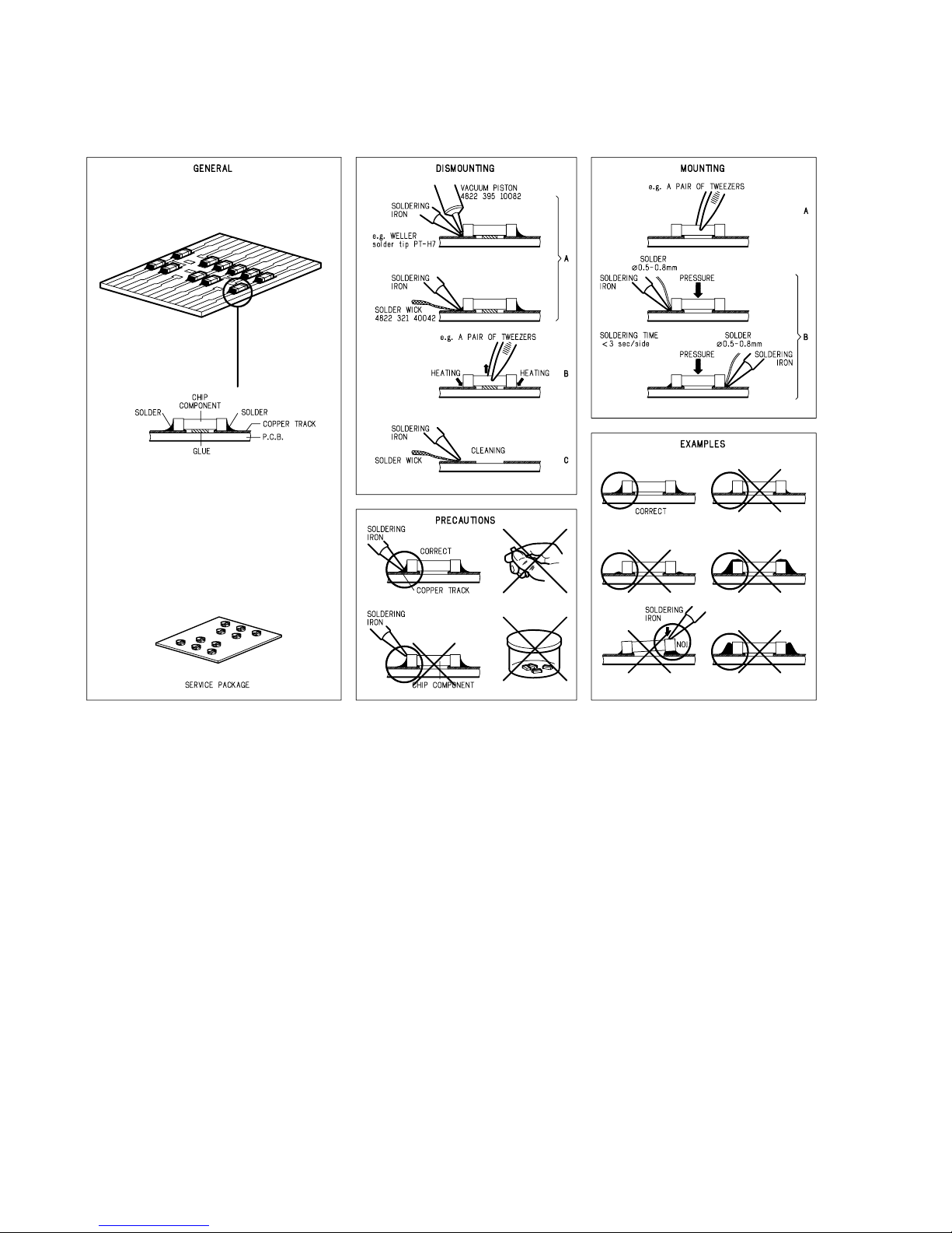
2. SERVICE HINTS AND TOOLS
DVD test disc (NTSC) ALMEDIO TDV-540
SERVICE TOOLS
Audio signals disc 4822 397 30184 or TCD-784
Disc without errors +
Disc with DO errors, black spots and fingerprints 4822 397 30245 (SBC444A) or TCD-726
Disc (65 min 1kHz) without no pause 4822 397 30155
Max. diameter disc (58.0 mm) 4822 397 60141
Torx screwdrivers
Set (straight) 4822 395 50145
Set (square) 4822 395 50132
13th order filter 4822 395 30204
DVD test disc (PAL) 4822 397 10131
SERVICE HIN
TS
070703MZ
Page 7

5
3. WARNING AND LASER SAFETY INSTRUCTIONS
F
ATTENTION
Tous les IC et beaucoup d’autres semiconducteurs sont sensibles aux décharges
statiques (ESD).
Leur longévité pourrait être considérablement
écourtée par le fait qu’aucune précaution
n’est prise a leur manipulation.
Lors de réparations, s’assurer de bien être
relié au même potentiel que la masse de
l’appareil et enfiler le bracelet serti d’une
résistance de sécurité.
Veiller a ce que les composa
nts ainsi que les
outils que l’on utilise soient également a ce
potentiel.
D
WARNUNG
Alle IC und viele andere Halbleiter sind
empfindlich gegen elektrostatische
Entladungen (ESD).
Unsorgfältige Behandlung bei der Reparatur
kann die Lebensdauer drastisch vermindern.
Sorgen sie dafür, das Sie im Reparaturfall
über ein Pulsarmband mit Widerstand mit
dem Massepotential des Gerätes verbunden
sind.
Halten Sie Bauteile und Hilfsmittel ebenfalls
auf diesem Potential.
WAARSCHUWING
Alle IC’s en vele andere halfgeleiders zijn
gevoelig voor elektrostatische ontladingen
(ESD).
Onzorgvuldig behandelen tijdens reparatie
kan de levensduur drastisch doen
verminderen.
Zorg ervoor dat u tijdens reparatie via een
polsband met weerstand verbonden bent met
hetzelfde potentiaal als de massa van het
apparaat.
Houd componenten en hulpmiddelen ook op
ditzelfde potentiaal.
AVVERTIMENTO
Tutti IC e parecchi semi-conduttori sono
sensibili alle scariche statiche (ESD).
La loro longevita potrebbe essere fortemente
ridatta in caso di non osservazione della piu
grande cauzione alla loro manipolazione.
Durante le riparazioni occorre quindi essere
collegato allo stesso potenziale che quello
della massa dell’apparecchio tramite un
braccialetto a resistenza.
Assicurarsi che i componenti e anche gli
utensili con quali si lavora s
iano anche a
questo potenziale.
All ICs and many other semi-conductors are
susceptible to electrostatic discharges (ESD).
Careless handling during repair can reduce
life drastically.
When repairing, make sure that you are
connected with the same potential as the
mass of the set via a wrist wrap with
resistance.
Keep components and tools also at this
potential.
WARNING
Safety regulations require that the set be restored to its original condition
and that parts which are identical with those specified be used.
Veiligheidsbepalingen vereisen, dat het apparaat in zijn oorspronkelijke
toestand wordt terug gebracht en dat onderdelen, identiek aan de
gespecifieerde worden toegepast.
Bei jeder Reparatur sind die geltenden Sicherheitsvorschriften zu beachten.
Der Originalzustand des Gerats darf nicht verandert werden
.
Fur Reparaturen sind Original-Ersatzteile zu verwenden.
Le norme di sicurezza esigono che l’apparecchio venga rimesso nelle
condizioni originali e che siano utilizzati pezzi di ricambiago idetici a quelli
specificati.
Les normes de sécurité exigent que l’appareil soit remis a l’état d’origine et
que soient utilisées les pièces de rechange identiques à celles spécifiées.
“Pour votre sécurité, ces documents
doivent être utilisés par des
spécialistes agrées, seul s habilités à
réparer votre appareil en panne.”
GB
NL
I
D
I
F
GB
NL
LASER SAFETY
CAUTION VISIBLE AND INVISIBLE LASER RADIATION WHEN OPEN AVOID EXPOSURE TO BEAM
ADVARSEL SYNLIG OG USYNLIG LASERSTRÅLING VED ÅBNING UNDGÅ UDS
Æ
TTELSE FOR STRÅLING
ADVARSEL SYNLIG OG USYNLIG LASERSTRÅLING NÅR DEKSEL Å PNES UNNGÅ EKSPONERING FOR STRÅLEN
VARNING SYNLIG OCH OSYNLIG LASERSTRÅLNING NÄR DENNA DEL ÄR ÖPPNAD BETRAKTA EJ STRÅLEN
VARO! AVATT AESSA OLET ALTTIINA NÄKYVÄLLE JA NÄKYMÄTTÖMÄLLE LASER SÄ
TEILYLLE. ÄLÄ KATSO SÄTEESEEN
VORSICHT SICHTBARE UND UNSICHTBARE LASERSTRAHLUNG WENN ABDECKUNG GEÖFFNET NICHT DEM STRAHL AUSSETSEN
DANGER VISIBLE AND INVISIBLE LASER RADIATION WHEN OPEN AVOID DIRECT EXPOSURE TO BEAM
ATTENTION RAYONNEMENT LASER VISIBLE ET INVISIBLE EN CAS D'OUVERTURE EXPOSITION DANGEREUSE AU FAISCEAU
USE OF CONTROLS OR ADJUSTMENTS OR PERFORMANCE OF PROCEDURE OTHER THAN THOSE
SPECIFIED H
EREIN MAY RESULT IN HAZARDOUS RADIATION EXPOSURE.
AVOID DIRECT EXPOSURE TO BEAM
WARNING
The use of optical instruments with this product will increase eye hazard.
Repair handling should take place as much as possible with a disc loaded inside the player
WARNING LOCATION: INSIDE ON LASER COVERSHIELD
This unit employs a laser. Only a qualified service person should remove the cover or attempt to service t
his
device, due to possible eye injury.
030804ecm
Page 8

6
4. SERVICE MODE AND TAKING THE DISC
OUT OF EMERGENCY
[A] SERVICE MODE
電源コードを接続します。( STANDBY モードにします)1.
2. g/iボタンとSTOPボタンを押しながらPOWER ON/
STANDBYボタンを押します。
DISPLAYに機種名が表示されます。
3. g/iボタンを押します。
DISPLAYにMicro-Processor Versionが表示されます。
4. g/iボタンを押します。
FLDが全点灯します。
5. g/iボタンを押します。
DISPLAYにSERIAL NOが表示されます。
6. g/iボタンを押します。
DISPLAYにDISC 再生時間(総合計)が表示されます。
いつでも前の表示に戻るには、H/Eボタンを押します。
電源を切るとSERVCICE モードが解除されます。
4. SERVICE MODE AND TAKING THE DISC
OUT OF EMERGENCY
[A] SERVICE MODE
Insert mains cable plug in the outlet. (The Unit is standby 1.
mode.)
Press the 2. POWER ON/STANDBY button While pressing
g/i button and STOP Button.
Model name is displayed.
Press 3. g/i button
Version of microprocessor is displayed.
Press 4. g/i button
Light up all FL segment
Press 5. g/i button
Serial number is displayed.
Press 6. g/i button
Playback time is displayed.
To return to a previous display at anytime, press H/E
button.
Press the POWER ON button to quit Service Mode.
[B] TAKING THE DISC OUT OF EMERGENCY
Remove the top cover of the player.1.
Remove 2 screws shown in the picture 2.
follows.
Remove the disc clamper.3.
Now you can remove the disc.4.
CD5003
20 0 8 - 05 -16-1
MZ_000000000
PTime : 00021h
Remove those screws
DISC
TTL
TRK
PEAK
TTL
TIME
RNDM
PROG
A – B RPT 1
PITCH
EDIT
TEXT
1 2 3 4 5 6 7 8 9 10 11 12 13 14 15 16 17 18 19 20
Page 9

7
5. DISC再生時間のリセット(初期化)方法
新しいCD MECHANISM (TRAVERSE)に交換した場合、次の
手順でDISC再生時間をリセット(初期化)してください。
SERVICE MODE の手順6. でDISPLAYにDISC 再生時間(1.
合計)が表示されます。
表示は時間単位です。(例:10050時間0分1秒は10051h
となります)
最大表示は、65536hまでです。
2. C (STOP)ボタンを3秒以上押します。
DISPLAYにPTime Clear?と表示されます。
3. B (PLAY)ボタンを押します。
DISPLAYにDoneと表示され、その後、PTime:00000hと
なります。
DISC再生時間がリセット(初期化)されました。
電源を切るとSERVCICE モードが解除されます。
5. HOW TO THE RESET OF PLAYBACK TIME
When replacing CD MECHANISM (TRAVERSE), please
reset Playback time (total) in the following procedure.
Procedure 6 of SERVICE MODE, Playback time (total) is 1.
displayed.
The display is a time unit. (Example: "10050 hours, 0
minute, 1 second " is 10051h)
The maximum Playback time is 65536h.
Press 2. C (STOP) Button 3 seconds and more.
PTime Clear? is displayed.
Press 3. B (PLAY) Button.
Done is displayed after PTime:00000h is displayed.
Play back time (total) was reset.
Press the POWER ON button to quit Service Mode.
PTime : 10051h
PTime Clear?
Done PTime : 00000h
Page 10

8
6. UPDATE MICROPROCESSOR SOFTWARE
PROCEDURE
マイコンのソフトウェアが更新された場合、下記の手順に従っ
てアップデートしてください。
必要機器
• Windows PC (OS: Windows 2000またはWindows XP) で
Serialポートのあるもの
• RS-232Cストレートケーブル (9pinメス−9pinメス)
• 接続冶具 (90M-SR4500JIG)
• アップデート用書き込みソフトウェア (Flash Programmer
フォルダ内 FlashProg.exe、および他のファイルとフォル
ダ)
• アップデート用データ (CD5003_yymmdd_x.s24)
注意 : yyは年の下二桁、mmは月、ddは日、xはリリースナン
バー
[A] Update Procedure
1. "Flash Programmer"と"software"フォルダをPCの任意のフ
ォルダにコピーします。
2. "Flash Programmer"フォルダをダブルクリックします。
6. UPDATE MICROPROCESSOR SOFTWARE
PROCEDURE
When microprocessor software was updated, update the
software in the following procedure.
Necessary Equipment
• Windows PC (OS: Windows 2000 or Windows XP) with
Serial port.
• RS-232C Dsub-9 pin cable (female to female/straight
type).
• Connection JIG (90M-SR4500JIG)
• Update tool (FlashProg.exe, other files and folders in
Flash Programmer folder)
• Update data (CD5003_yymmdd_x.s2h4)
NOTE : The yy is two digits of year. The mm is month. The
dd is date. The x is release number.
[A] Update Procedure
1. Put the "Flash Programmer" and "software" folder into
anywhere on your PC’s hard disc.
2. Double click the "Flash Programmer" folder.
CD5003
CD5003
Page 11

9
3. FlashProg.exeをダブルクリックし、Flash Programmerを
起動します。
注意 : FlashProg.exeをダブルクリックしてもFlash
Programmer が起動しない場合は、"[B] When a Flash
Programmer did not launch"を参照してください。
4. OKをクリックします。
注意 : は本機に自動的に通信接続を行います。このダイアログ
ボックスは通信接続に失敗すると常に表示されます。
3. Double click FlashProg.exe, and launch the Flash
Programmer.
NOTE : When a Flash Programmer does not launch even if
double-clicked FlashProg.exe, please refer to "[B]
When a Flash Programmer did not launch".
4. Click OK.
NOTE : Since Flash Programmer communicates with the
unit automatically, the following dialog box appears
when it fails in communication.
Page 12
10
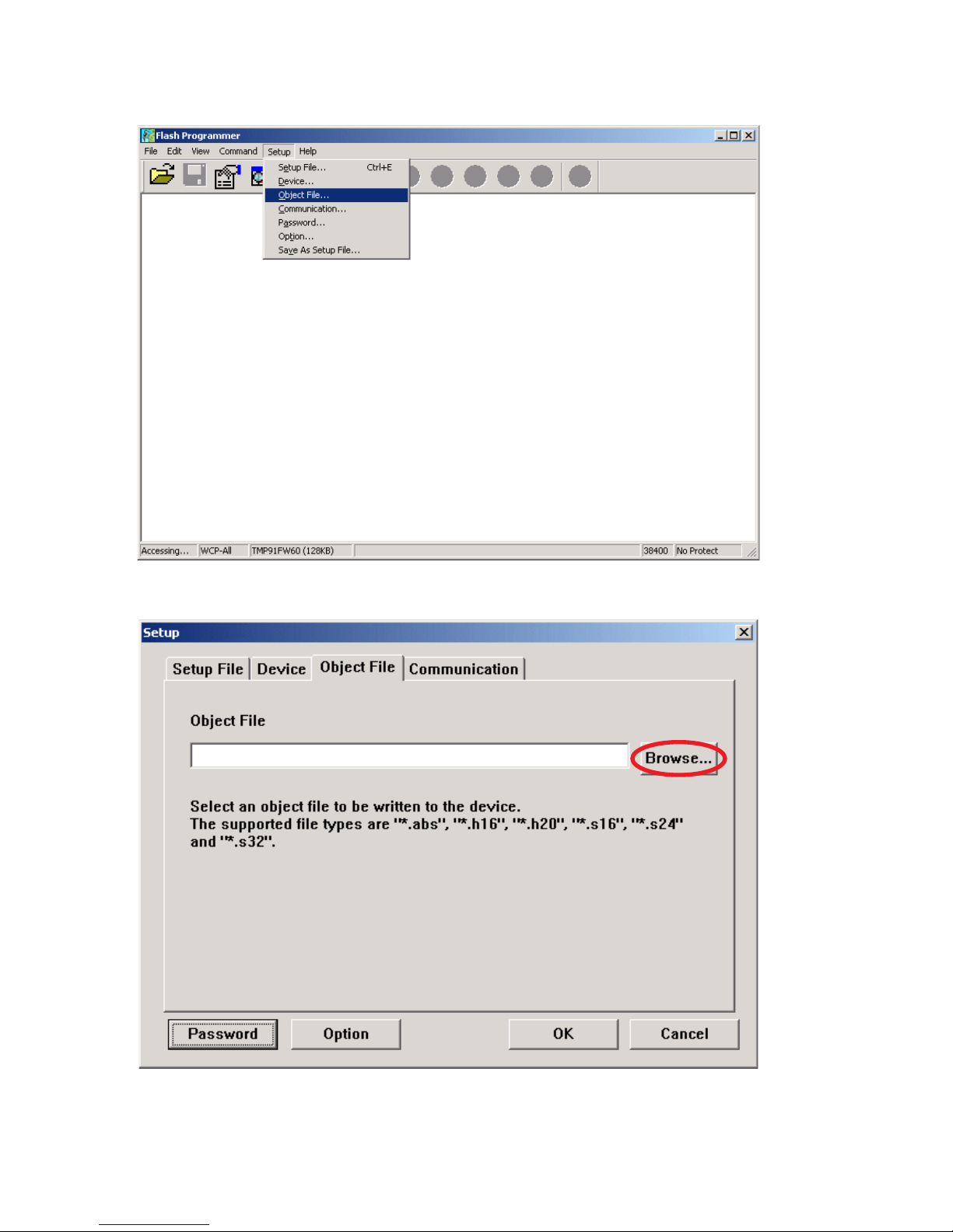
5. メニューバーからSetupをクリックし、Object fileを選択
します。
6. Browseをクリックします。
5. Click the Setup in the menu bar and select the Object
file.
6. Click Browse.
Page 13

11
7. Files of type をMotorola S Format(*.s16,*.s24,*.s32)に
変更します。
CD5003_yymmdd_x.s24を選択し、Openをクリックし
ます。
注意 : yyは年の下二桁、mmは月、ddは日、xはリリースナン
バー
8. Deviceタブをクリックします。
7. Choose the Motorola S Format(*.s16,*.s24,*.s32) in
Files of type.
Choose the CD5003_yymmdd_x.s24, and click Open.
NOTE : The yy is two digits of year. The mm is month. The
dd is date. The x is release number.
8. Click Device tab.
CD5003_yymmdd_x.s24
CD5003_yymmdd_x.s24
Page 14

12
9. DeviceからTMP91FW60を選び、Seriesから900/L1を選択
します。
そして、Communicationタブをクリックします。
10. COM Portから使用するポート番号を選択します。
Data Rate Manualにチェックを入れ、Data Rareから
38400を選択します。
OKをクリックします。
9. Choose the TMP91FW60 in the Device, and choose the
900/L1 in the Series.
And click Communication tab.
10. Choose the Serial port number in the COM Port.
Check the Data Rate Manual, and choose the 38400 in
the Data Rare.
And Click OK.
Page 15

13
11. 本機から電源ケーブルを外します。
12. 接続冶具のRS-232C端子とPCのSerialポートをRS-232C
ケーブルで接続します。
13. 本機のリアパネルに接続冶具のFFC をコンタクト面を上に
して差し込みます。
14. 本機に電源ケーブルを接続します。
15. Flash Programmerが通信接続に成功すると"Erase All data
in this devise? (Y/N)"と書かれたダイアログボックスが自動
的に表示されます。接続に失敗するとエラーメッセージが
表示されます。(例:E000)
Yesをクリックします。
16. OKをクリックします。
11. Disconnect the mains cord from the unit.
12. Connect the RS-232C on the connection JIG and the
Serial Port of windows PC with RS-232C cable.
13. Connect FFC (upside contact) to the rear panel of the
unit from connection JIG.
14. Connect the mains cord into the unit.
15. If the connection with the Flash Programmer is
successfully made, a dialogue box saying "Erase All
data in this devise? (Y/N)" appears automatically. If the
connection fails, error message will appear. (Ex.: E000)
Click Yes.
16. Click OK.
Page 16

14
17. P (Program)をクリックし、アップデートを開始します。
18. ソフトウェアがマイコンに書き込まれます。
ソフトウェアの書き込みにかかる時間はおよそ50秒です。
19. アップデートが完了すると"R006: Programming
completed successfully"と書かれたダイアログボックスが
表示されます。
OKをクリックします。
17. Click P (Program) to start update.
18. Software is written into the microprocessor.
The writing of software takes about 50 seconds.
19. If the software is updated successfully, a dialog box
saying "R006: Programming completed successfully."
appears.
Click OK.
Page 17

15
20. メニューバーのFileをクリックし、Exitを選択します。
21. 電源ケーブルを本機からはずし、その後接続冶具のFFCを
本機から外します。
[B] When a Flash Programmer did not launch
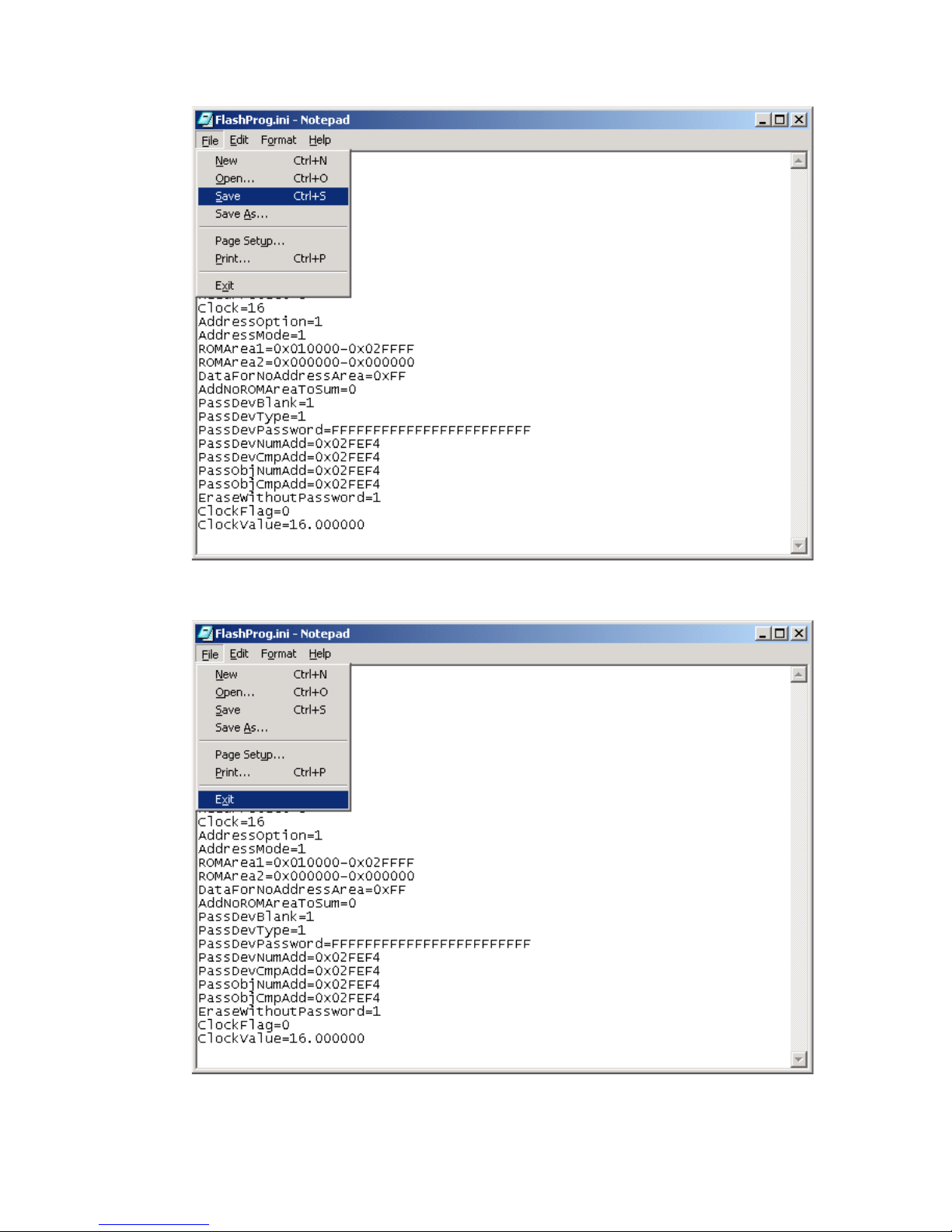
1. Flash Programmerフォルダ内のFlashProg.iniをテキスト
エディタで開きます。(メモ帳など)
20. Click the File in the menu bar and select the Exit.
21. Disconnect mains cord from the unit, and then disconnect
FFC of connection JIG from the unit.
[B] When a Flash Programmer did not launch
1. Open the FlashProg.ini in the Flash Programmer folder
by text editor. (EX.: Notepad, etc)
Page 18

16
2. テキスト文のOpenFile=C:\...(PC環境により異なりま
す。)...\???.s24を削除します。
2. Delete the text "OpenFile=C:\...(your PC setting)...\???.
s24".
Page 19
17
3. FlashProg.iniを上書き保存します。
4. テキストエディタを閉じます。
5. これでFlash Programmerを起動することが出来ますので
[A] Update Procedure手順3に戻ってください。.
3. Save the FlashProg.ini.
4. Close the text editor.
5. Probably you can launch the Flash Programmer. Go to
the [A] Update Procedure step 3.
Page 20

18
Personal notes:
Page 21

19 20
MAIN TRANSF
CD MECHANISM
WELCOME
FRONT PWB
DSP
MCU
(UPDATE PORT)
B TYPE
ANGLE TYPE
BN51
CN51
AC
7P
INLET
RELAY
SUB
TRANS
NL
N
N
BLACK
RED
WHITE
BLACK
21P
B TYPE
16P
B TYPE
MAIN PWB
AUDIO PWB
POWER PWB
TRANSF. PWB
HEADPHONE PWB
FLASHER PWB
TACT SW PWB
BN45 CN45
BN44
CN93
CN94
CN91
CN92
BN93 BN94
CN44
CN21
CN33
CN31 CN32
CN42
CN43
CN41
BN41
BK21 CN22
SW41
JK43
JK41
JK42CN23
BK91
BN43
JK71
BK75
JK61
BN42
CN81
BN81
PH81
VR81
CN21
BN92
CORE
CORE
JW51
BK81
SCREW
CORE
CORE
7. WIRING DIAGRAM
Page 22

2221
UPDATE
RST/ST+5V/GND
DMO
FMO
TR+/-
FC+/-
LOGIC
CONTROL
SPINDLE+
SPINDLE-
SLED+
SLED-
TRACKING+
TRACKING-
FOCUS+
FOCUS-
SPINDLE MOTOR
SLED MOTOR
SPINDLESPINDLE+
SLEDSLED+
LIMIT SW
CL/SW
COM
20Mhz
LOADING+
LOADING-
SERIAL
PORT
VOLUME
Control
MIXER
VOLUME
Control
INTERPOLATION
FILTER
FILTER
INTERPOLATION
DAC
DAC
ANALOG
FILTER
FILTER
ANALOG
MODE
Selector
Control
Port
SDATA
SCLK
LRCK
DAC_MCK
NC (DAC_SDA)
NC
NC
NC (DAC_SCL)
AOUTB-
AOUTB+
AOUTA+
AOUTA-
MDI
LDO
EXTERNAL
Mute Control
Reference
CMOUT FILT+
DOUT
+3.3VA
SIO/UART
(SIO0)
SIO/UART
SIO/UART
(SIO1)
(SIO2)
I2C
I2C
(SBIO)
(SBI1)
8bit TIMER
8bit TIMER
8bit TIMER
8bit TIMER
8bit TIMER
8bit TIMER
(TMRA0)
(TMRA1)
(TMRA2)
(TMRA3)
(TMRA4)
(TMRA5)
(TMRB0)
16Bit TIMER
16Bit TIMER
16Bit TIMER
16Bit TIMER
16Bit TIMER
(TMRB1)
(TMRB2)
(TMRB3)
(TMRB4)
XWA
XBC
XDE
XHL
XIX
XIY
XIZ
XSP
W
B
D
H
A
C
E
L
IX
1Y
IZ
SP
32bit
F
P C
WATCH-DOG TIMER
Clock Timer
8 K B R A M
900/L1 CPU
High-speed
Oscillator
Oscillator
LOW-speed
MODE
CONTROLLER
INTERRUPT
CONTROLLER
INTERRUPT
CONTROLLER
DATA BUS
ADDRESS BUS
Memory
Controller
(blocks)
P O R T
1 0 - B I T
1 6 C H
A D
RL4
RL3
RL1
RL2
RL5
E
C
B
F
D
A
DAC_MCK DSP_MCK
PLL_SCL
PLL_SDA
DECODER
256X 1024
MEMORY ARRAY
COLUMN I/O
I/O
DATA
CIRCUIT
CONTROL
CIRCUIT
A0-A14
VCC
GND
I/O1-I/O7
CE1
OE
WE
VFD-CLK
VFD-CE
VFD-DI
VFD-POWER
REMO
VFD-CLK
VFD-CE
VFD-DI
VFD-POWER
RS/REMOTE_IN
RS/REMOTE_IN
SRAM_CE
SRAM_OE
SRAM_WE
ADDRESS PORT
DATA PORT
RST
ST+5V
DAC_RST
DAC_RST
PLL_SDA
PLL_SCL
+5VA
KEY DATA
LED DATA
KEY DATA
LED DATA
CD-BUS2
CD-BUS3
CD-BUCK
CD-CCE
CD-RST
MT-STBY
CL-M
OP-M
OP-SW
CL-SW
LIMIT-SW
OP-M
CL-M
MT-STBY
OP/SW
OP-SW
CL-SW
LIMIT-SW
SYS_DETECT
ST+5V
EXTERNAL
INTERNALHL
SYS_DETECT
SDATA
SCLK
LRCK
DSP_MCK
DMO
FMO
TRO
FOO
TRO
FOO
FOCUS-
FOCUS+
TRACKING-
TRACKING+
E
F
B
D
A
C
+3.3VA +5VA
16.9344 MHz
ST+5V
ST+5V
+P1.5V+3.3V3.3VDA+VREF
+RF3.3V
+VREF
+VREF +8V
A_MUTE
B_MUTE
+12V -12V
F_MUTE
A_MUTE
B_MUTE
F_MUTE
+3.3VCL
P_MUTE
P_MUTE
FL+/-FVDDVP FST+5V
+12V
-12V
A
B
VDD
VDD
INTERRUPT
89
PLL_SCL
PLL_SDA
ST+5V
PWR_D
T_ON/OFF
CMOS
LV
Divider
and
Output
Control
Programming
and
Control Register
+1.8V +3.3VCL
TC7WHU04FU
+3.3VCL
CMOS
LV
CMOS
LV
VDIS
GND
VOUT
VIN
GND
OUTIN
321
NC
OUT
DS
VSS
VDD
GND
OUTIN
GND
OUTIN
AUDIO+
AUDIO+
AUDIO-
+8V
VDD
+3.3V
3.3VDA
+P1.5V
VP
FL+
FL-
+8V
+8V
ST+5V
REMO
RS_REMOTE_IN
PWR_MUTE
B+
+3.3V +1.8V
u-COM
26 28 2122 3357 58 59 61 65 67
4
5
6
UPDATE PORT
44~
9~
52
53
54
55
56
92
90
SRAM
2019 7175 78
R A M
R A M
FLASH ROM 128KByte
ROM Correction
1868 35 307980 81 38
85
86
8776419
88
EEPROM
31 32
3 2
54
1
WELCOME
CLOCK(PLL+VCO)
DSP POWER
CDCE913
910121323
40
41
42
43
37
61
91
92
94
95
96
97
98
100
62 63 64
TC94A70FG
CD DSP
35
33
34
OPTICAL OUT
COAXIAL OUT
CD MECHANISM
SYS DETECT
DRIVE I.C
M
M
M
L
R
LPF (OP Amp IC)
HEADPHONE
OUTPUT
BUS IN/OUT
UPDATE PORT
ANALOG L
ANALOG R
+
Tr.Buffer
FLUSHER IN(U Ver ONLY)
PLL
with SSC
DAC (CS4392)
VCXO
XO
LVCMOS
EEPROM
321
321 321
43
21
321
321
MAIN TRANS
SUB TRANS
321
321
CD-RF
IN
CD-RF
Amp
Audio
DAC
Analog
Post
Filter
Servo
ADC
CDP
DSP
24-Bit
DSP
1 Mbit
SRAM
Servo
Processor
Servo
DAC
Peripheral
I/F
PLL/VCO
(Audio Out)
3.3V 1.5V
8. BLOCK DIAGRAM
Page 23

23 24
FCSTRKTRK+
FCS+
LD PD
LD VR
LD LD
PDIC GND
PDIC F
PDIC C
PDIC B
PDIC A
PDIC D
PDIC E
PDIC VCC
PDIC VC
MAIN PWB
KEY2
LED
KEY1
VFD-DI
VFD-CLK
VFD-CE
RESET
REMO
KEY0
DGND
STBY-LED
MP3_LED
RXTXRESET
VCC
GND
M/SEL
XI
XO
TNI
TNPC
TPI
FPI1
FPI2
FNI1
FNI2
RVSS3
MDI
LDO
RVDD3
TSETR
AGCI
RFO
VMDIR
RESIN
VRO
RFEQO
RFRPI
RFI
SLCO
PVSS3
VCOF
77:PVREF
76:LPFO
LPFN
TMAX
TMAXS
PDO
PVDD3
AWRC
VSS4
VDD1-3
LRCK1
BCK1
AIN
LRCK
BCK
AOUT
DOUTMSGPIN
ZDET
SFSY
IPF
SBOK
SBSY
VDDT3-1
VSS3
PIO3
PIO1
PIO2
PIO0
AOUT2
AOUT3
IRQ
TEST
CCE
BUCK
BUS3/SI
BUS2/SO
BUS1
BUS0
/RST
STBY
VDDM1
VDD1-2
VSS2
VDDT3
DVSS3-2
LO
DVR
DVDD3
RO
DVSS3
XVDD3
XO
XI
XVSS3
IO1/HSO
IO/HSO
FGIN
VSS1
VDD1-1
VDDP3
VCOI
VSSP3
DMO
FMO
VREF
TRO
FOO
AVDD3-1
TEZI
TEI
SBAD/RFDC
FEI
RFRP
1:AVSS3
2:RFZI
DSP POWER
KEY3
FIP2
FIP1VPVDD
+8V
ST+5V
PWR_MUTE
FIP2
FIP1
VP
AUDIO+
AGND
AUDIO-
TO AUDIOPWB
TO AUDIO PWB
FROM POWER PWB
KEY4
FROM POWER PWB
0 (N.C)
2.2K
2.2K
2
.2K
2.2K
0.01uF
0.1uF
18K
18K
18K
1uF
7654321
33P
33P
20Mhz
3.3K
470P
470P
0.047u
0.047u
8.2K
470
0.1uF
220u/16V
0
100/16V
10
1SS355T
A1504S
10uH
5 4 3 2 1654321
123 4 5 6 789 10 11 12 13 14 15 16 17 18
192021222324252627282930313233343536
TA2125AF
16
15
14
13
12
11
10
9
8
7
6
5
4
3
2
1
100/16V
0.1uF
47/25V
12P
220
TX
IN
VCC
GND
1 2 3
100
99
98
97
96
95
94
93
92
91
90
89
88
87
86
85
84
83
82
81
80
79
78
77
76
75747372717069686766656463626160595857565554535251
50
49
48
47
46
45
44
43
42
41
40
39
38
37
36
35
34
33
32
31
30
29
28
27
26
25 24 23 22 21 20 19 18 17 16 15 14 13 12 11 10 9 8 7 6 5 4 3 2 1
T5CD2
100K
0
1K1K1K
1K
47K
47K
47K
18K
0.1uF
0.1uF
47
1SS355T
2827262524232221201918171615
14 13 12 11 10 9 8 7 6 5 4 3 2 1
0
KRA102S
KRA102S
47/25V
0.1uF
100K
22P(NC)
22P(NC)
22P(NC)
0
0
0
0.1uF
470/16V
1000P
4700P
0.1uF
22K
0.01u
F
0.1uF
68P
0.1uF
0.015u
0.01uF
0.01uF
47/25V
0.1uF
0.033u
0.015u
47P
150K
330K
15K
47K
5.6K
15K
0.1uF
100K
100P(NC)
100P(NC)
100P(NC)
100P(NC)
0.1uF
0.1uF
0.1uF
100/16V
0.1uF
47/25V
0.1uF
0.1uF
220
0.1uF
2200P
12345678910111213141516171819202122232425
26
27
28
29
30
31
32
33
34
35
36
37
38
39
40
41
42
43
44
45
46
47
48
49
50
51 52 53 54 55 56 57 58 59 60 61 62 63 64 65 66 67 68 69 70 71 72 73 74 75
76
77
78
79
80
81
82
83
84
85
86
87
88
89
90
91
92
93
94
95
96
97
98
99
100
TC94A70FG
0.033u
0.033u
0.1uF
0.1uF
100
0.01uF
100/16V
0.01uF
0.01uF
0.01uF
0.01uF
100/16V
3
NC
OUT
DS
VSS
VDD
2
5 4
1
S-80145ALMC
0.1uF
0.1uF
0.1uF
100K
100K
100K
100/16V
KTC3875S
0.1uF
0.1uF
1000/6.3V
3 7
6
5
42
1
22
100P
0 2.2K
KTC3875S
1.8K
3.9K
220
(NC)
1uF
68
100K
0
0.1uF(NC)
0
(NC)
10
220/16V
0.1uF
In Out
GND
312
KIA1117S33
In Out
GND
312
KIA1117S15
0.1uF
100/16V
0.1uF
47/
25V
0.1uF
47/25V
1N4003SRT
100
0.1uF(NC)
KTA1267Y
4.7K
47K
KRC111S
2.2/50V
15K
1.2K
KRC111S
10K
2200/25V
1SS355T
100/16V
0.1uF
100/16V
0.1uF
0.1uF
100/16V
0.1uF
321321
0
0
8 765
4321
TC7WHU04FU
212019181716151413121110987654321
8765
4 3 2 1
AT24C02
IS61C256AL
0.1uF
1K
11 10 9 8 7 6 5 4 3 2 1 123
4.7V
10
10
13121110987654321
1SS355T
1SS355T
1SS355T
0
KTC3199Y
5.6V
4.7K
(N.C)
14 13 12 11 10 9 8
7654321
CDCE913PWR
1M(N.C)
15P
15P
16.9344MHz
270
In Out
GND
312
1.8V
100/16V
0.1uF
47/25V
0.1uF
0.1uF
0.1uF
22
0
0
0.1uF(N.C)
0.1uF(N.C)
0
0
0(N.C)
0(N.C)
10K
10K
0.1uF
10K
10K
0.1uF
47/25V
0.1uF
0.1uF
0.1uF
10K
3.3K
1SS355T
47K
0
1K
0.1uF
0.1uF
TR+
TR-
FC+
FC-
SLED+
SLED-
SPINDLE+
SPINDLE-
MT-STBY
CD-OPEN-M
CD-CLOSE-M
PD
T
R-
FC+
FC-
TR+
DAGND
DAGND
CD
HOST
DGND
DGND
MGND
MGND
DGND
DGND DGND DGND DGND
VFD-CE
VFD-CLK
VFD-DI
DGND
DGND
DGND
DGND
DGND
CD-BUS2
CD-BUS3
CD-BUCK
CD-CCE
CD-OPEN-SW
CD-CLOSE-SW
CD-LIMIT-SW
DGND
DAC_RST
F_MUTE
DGND
DGND
S_RAM_DATA00
S_RAM_DATA01
S_RAM_DATA02
S_RAM_DATA03
S_RAM_DATA04
S_RAM_DATA05
S_RAM_DATA06
S_RAM_DATA07
S_RAM_ADD07
ST+5V
VDD
LED
KEY0
KEY1
KEY2
VFD_POWER
VFD_POWER
STBY-LED
HOST
VDD
DGND
DGND
SRAM_CE
SRAM_OE
SRAM_WE
DGND
3.3VDA
3.3VDA
ST+5V
ST+5V
ST+5V
ST+5V
CD-RST
MT-STBY
CD-CLOSE-M
VFD-CE
VFD-DI
VFD-CLK
TRANS_ON/OFF
MP3-LED
MP3-LED
KEY0
KEY1
KEY2
S_RAM_ADD08
S_RAM_ADD09
S_RAM_ADD10
S_RAM_ADD11
S_RAM_ADD12
S_RAM_ADD13
S_RAM_ADD14
S_RAM_ADD06
S_RAM_ADD05
S_RAM_ADD04
S_RAM_ADD03
S_RAM_ADD02
S_RAM_ADD01
S_RAM_ADD00
RS_ON/OFF
SYS_DETECT
HOST-RST
S_RAM_DATA03
S_RAM_DATA04
S_RAM_DATA05
S_RAM_DATA06
S_RAM_DATA07
SRAM_CE
S_RAM_ADD10
SRAM_OE
S_RAM_ADD11
S_RAM_ADD09
S_RAM_ADD08
S_RAM_ADD13
SRAM_WE
S_RAM_DATA02
S_RAM_DATA01
S_RAM_DATA00
S_RAM_ADD00
S_RAM_ADD01
S_RAM_ADD02
S_RAM_ADD03
S_RAM_ADD04
S_RAM_ADD05
S_RAM_ADD06
S_RAM_ADD07
S_RAM_ADD12
S_RAM_ADD14
CD-OPEN-M
RS/REMOTE_IN
DGND
DGND
DGND
DGND
DGND
DGND
DGND
CD-BUS2
CD-BUCK
CD-CCE
CD-BUS3
CD-RST
DGND
DGND
+3.3V
+P1.5V
+3.3V
DGND
SDATA
SCLK
LRCK
+P1.5V
3.3VDA
DAGND
3.3VDA
DAGND
E
F
B
D
A
C
PD
C
F
B
A
D
E
3.3VDA
+P1.5V
3.3VDA
+3.3V
DGND
DSP_MCK
+3.3V
+VREF
+VREF
LOADING-
LOADING+
ST+5V
STBY-LED
CD-LIMIT-SW
LOADING-
LOADING+
CD-OPEN-SW
CD-CLOSE-SW
DGND
DGND
DGND
DGND
DGND
DGND
DGND
+VREF
HOST-RST
ST+5V
PLL_SDA
PLL_SCL
DGND
DGND
DAGND
VFD_MUTE
DGND
DGND
DGND
DGND
DAGND
RS_ON/OFF
VDD
DNGDDNGD
DGND DGND
DGND
DGND
DGND
DGND
DGND
DGND
DAC_RST
SDATA
SCLK
LRCK
DAC_MCK
F_MUTE
VDD
DGND DGND
DGND
DGND
DGND DGND
DGND
DGND
SYS_DETECT
DGND
DGNDDGND
DGND
DGNDDGND
REMO
RS/REMOTE_IN
VFD_MUTE
DGND
DGND DGND
DGND
TRANS_ON/OFF
DGNDDGND
KEY3
REMO
RS/REMOTE_IN
ST+5V
DGND
KEY3
DGND
DSP_MCKDAC_MCK
DGND
LED
DGND
KEY4
KEY4
DGND
DGND
EEPROM_SDA
EEPROM_SCL
DGND
MGND
DGND
SLED+
SLED-
SPINDLE-
SPINDLE+
HOST-RST
PLL_SDA
PLL_SCL
ST+5V
+3.3V
3.3VDA
+P1.5V
+8V
VDD
VDD
+8V
ST+5V
INTERRUPT
INTERRUPT
PWR_D
DGND
DGND DGND
DGND DGND
DGND
DGND
DGND
+1.8V
+1.8V +1.8V DGND
DGND
DGND
+3.3VCL
DGND
DGND
DGND
DAGND
DAGND
DAGND
DAGND
DAGND
DAGND
DAGND
EEPROM_SDA
EEPROM_SCL
+3.3VCL
DGND
DGND
ST+5V
+3.3VCL
+3.3V
DGND
DAGND
DGND
DAGND
DAGND
MGND
MGND
DGND
DAGND
DGND
PWR_D
DGND
DGND
CHGND
DGND
DGND
OPTICAL OUT
COAXIAL OUT
TO/FROM
CD MECHANISM
TO/FROM
CD MECHANISM
TO/FROM
CD MECHANISM
TO/FROM FRONT PWB
R305
R304
R303
R302
R301
C337
C333
R322
R324
R323
C207
CN23
C202
C201
X201
R327
C335
C334
C339
C338
R326
R325
C340
C341
R320
C328
R321
D301
Q301
L303
CN31
CN32
IC32
CN33
C326
C404
C405
C403
R401
JK41
JK42
IC21
R202
R203
R204
R205
R206
R207
JK43
R415
R414
R416
R417
C411
C412
R418
D401
IC23
RAM
R210
Q202
Q201
C218
C219
R201
C307
C308
C309
R311
R312
R313
C324
C325
C329
C317
C318
R319
C319
C320
C323
C322
C321
C316
C315
C313
C312
C311
C314
C310
R317
R316
R318
R315
R314
R310
C306
R306
C305
C304
C303
C302
C301
C351
C350
C349
C348
C346
C347
C344
R328
C343
C342
IC31
C332
C331
C345
C330
R213
C220
C221
C206
C214
C215
C203
C216
IC24
C211
C212
C213
R308
R309
R307
C327
Q402
C208
C410
SW41
C336
CN22
R404
C406
L301
R405
R406
Q401
R407R408
R409
C407
C408
R410
R411
R412
C409
R413
R402
R403
C401
C402
L401
IC33
IC34
C363
C362
L302
C365
C364
C361
C360
D432 R435
C432
Q431
R434
R433
Q432
C433
R436
R431
Q433
R432
C431
D433
C462
C461
C466
C465
C468
C467
C210
CN43
CN44
R253
R254
IC26
CN21
IC22
C209
R212
CN42
CN41
D431
R251
R252
CN45
D202
D203
D204
R211
Q434
D434
R437
R438
IC27
R263
C261
C260
X251
R262
IC25
C251
C252
L252
C253
C254
C259
C258
R261
R258
R257
C256
C257
R361
R362
R256
R255
R259
R260
L251
C255
R208
R209
C222
C223
C352
C353
C354
R214
R329
D435
R439
R363
R440
C990
C991
TO FLASHER PWB
(U Ver ONLY)
9. SCHEMATIC DIAGRAM
MAIN PWB
Page 24

2625
AUDIO_AC2
AUDIO_AC1
2.5V
2.5V
2.5V
2.5V
VFD-DI
MP3&WMA
DISPLAY ON/OFF
!
!
CHASSIS BLACKET
BK91
(MGND)
N,F VER.
U VER.
D921
D920
JUMPER JUMPER
1N133MT 1N133MT
JW51
(CHASSIS)
1SS133MT
1SS133MT
1.0
1.0
8
7
3
2
1
47/25V 68
68
47/25V
4.7K
4.7K
4.7K
4.7K
100/16V
100/16V
P0001P0001
10K
10K
4.7K
4.7K
33 33
1SS133MT1SS133MT
1.5K
12
K5.121
KTC3203YT
KTA1271YT
KTA1271YT
KTC3203YT
1.5K12121.5K
1SS133MT
1SS133MT
3333
68
470/16V
100/16V
0.022u
1000/25V
47K
1K
C2316YT
470/16V
3300/25V
1N4003
1N4003
InOut
GND
213
KIA7912PI
3300/25V
1N4003
1N4003
12K
3.3K
1K
22K
0.1uF
104(100V)
10/50V
2.2/50V
220/63V
1N4003
C2316YT
36V
0.1uF
0.1uF
4700/35V
470/16V
100/16V
100
100
1N4003
1N4003
123
INOUT
GND
KIA7805API
1.2K
1.2K
KRA104MT
KRC107MT
220
47K
68
100P(N.C)
KTC2874
4.7K
470K
4.7K
68
KTC2874
1SS133MT
1SS133MT
220
KRC107MT
KRA104MT
1SS133MT
1SS133MT
KTC2874
68
4.7K
470K
4.7K
KTC2874
100P(N.C)
68
47K
100/16V
100/16V
123
INOUT
GND
KIA7808API
1 2 3 4
5678
A
+ -
B
+-
A OUTPUT
A-INPUT
A+INPUT
V-
B+INPUT
B-INPUT
B OUTPUT
V+
NJM2068MDTE1
4.7K
4.7K
47/25V
47/25V
47
47
470/16V
123
INOUT
GND
KIA7812API
1N4003
1N4003
6.2V
4.7K
1500P
0.1uF
GND
OUT IN
321
1.0
2.7K
47/25V
22/50V
22/50V
0.1uF
0.1uF
47/25V
750
3300P
10K
100P(FILM)
330P
2.7K
820
7.5K
2.2K
7.5K
120P
12345678910
11 12 15 16 17 18 19 201413
KTA1268
KTC3200
3.9K
33
33
3.9K
33
33
33
33
3.9K
33333.9K
KTC3200
KTA1268
1 234
5678
A
+-
B
+ -
A OUTPUT
A-INPUT
A+INPUT
V-
B+INPUT
B-INPUT
B OUTPUT
V+
NJM2068MDTE1
7.5K
2.2K
7.5K
820
2.7K
330P
100P(FILM)
10K
3300P
750
47/25V
2.7K
1000P
1500P
1 2 3 4 5 6 7 8 9 10 11
1.0
1.0
1.0
47/25V
47/25V
10K(NC)
10K(NC)
0.1uF
220/16V
InOut
GND
312
100/16V
220/25V
1 2 3
F2F2F2
VSS
VSS
VDD2
STB
BLK
VDD1
CLK
DI
D0
F1F1F1
444342403938373635343332321
14 13 12 11 10 9 8
7654321
321
VccGNDVOUT
RPM6936
0.1uF
47/16V
1 2 3 4 5
1 2 3 4 5
KRC107MT
1.8K
STANDBY
STANDBY
PAUSE
SKIP/SEARCH +
S
KIP/SEARCH -
STOP
K1K1
KRC107MT
560
OPEN/CLOSE
PLAY
47/16V
KRC107MT
560
0.1uF
0.1uF
100
K01K01
10K
10K
100
SIR-34ST3F
ROUTGND Vcc
1 2 3
RPM6936
0.1uF
100/16V
100
KRA102MT
2.7K
220/16V
220/16V
123456789101112131415161718192021
10K
1SS133MT
1SS133MT
0.1uF(NC)
21
1
4
2
3
SDT-S-112DMR
3.3K
10K
4700P(AC250V)
100/25V
100/25V
KSC2785Y
*
1.0
1SS133MT
1SS133MT
1 2 3 4 5 6 7
7654321
1 2 3
NC(0.1uF)
NC(0.1uF)
1 2 3
1 2 3
10K
5.6V
1N4003
1N4003
1N4003
1N4003
1234
5 678
A
+ -
B
+-
A OUTPUT
A-INPUT
A+INPUT
V-
B+INPUT
B-INPUT
B OUTPUT
V+
NJM2068MDTE1
(OPEN)
(OPEN)
(OPEN)
0.1uF
CHASSIS
1 2 3 4 5 6 7 8 9 10 11 12 13
1 2 3
2 1
1000P
4.7K
(N.C)
100
1000P
100P(FILM)
KTC3200
KTA1268
4.7K
1000P
(N.C)
100
100P(FILM)
KTA1268
KTC3200
47K(N.C)
47K(N.C)
KTC2874
KTC2874KTC2874
KTC2874
*
HDGND
DNGDHDNGDH
HDGND
HDGND
HDGND
HDGND
HDGND
HDGND
HDGND
HDGND
HD
GND
HDGND
MUTE_L
MUTE_R
DGND
DGND DGND
DGND DGND
AGND
AGND
AGND
AGND
DGND
DGND DGND DGND
DGND
DGND
DGND
DGND
DGND DNGDDNGD
DGND
DGND
DGND
DGND
GND
GND
GND
F_MUTE
GNDGND GND
GND
F_MUTE
A_MUTE
B_MUTE
GND
GND
GND
GND
GND
AGND
DGND
A_MUTE
GND
GND
F_MUTE
PWR_MUTE
PWR_MUTE
GND
GND
GND
AGND
AGND
GND
B_MUTE
GND
GND
AGND
DGND
LDGND
LST+5V
FST+5V
FRONT
FDGND
FST+5V
FDGND
FDGND
FDGND
FST+5V
FDGND
FDGND
V-CLK
FDGND
FVDD
VP
FDGND
VFD-POWER
FVDD
FIP2
FIP1
FDGND
FDGND
FST+5V
LDGND
FDGND
FST+5V
FST+5V
FDGND
KEY0
KEY1
KEY2
STBY-LED
VFD-DI
VFD-CLK
VFD-CE
VFD-POWER
MP3-LED
REMO
VP
LED
MP3-LED
REMO
KEY0
STBY-LED
KEY1
FST+5V
KEY3
FLUS_DGND
GNDGNDGND
GND
GND
GND
GND
GND
GND
GND
DGND
LED
KEY4
FDGND
FDGND
KEY2
KEY3
FDGND
FDGND
FDGND
KEY4
FST+5V
GND
DGND
TRANS_ON/OFF
GND
GND
GND
GND
GND
GND
GND
GND
DGND
TRANS_ON/OFF
FDGND
FIP1
FIP2
DGND
DGND
DGND
DGND
FCHGND
FCHGND
DGND
VFD-CE
V-CLK
VFD-CLK
VFD-DI
V-CE
V-CE
AUDIO+
AUDIO-
AUDIO+
AUDIO-
AUDIO+
+12V
-12V
+12V
-12V
-12V
ST+5V
ST+5V
ST+5V
FVDD
B+
+8V
+8V
B+
GND
GND
DGND
*
FST+5V
AGND
DGND
GND
GND
GND
GND
GND
-12V
MUTE_L
MUTE_R
HDGND
GND
GND
GND
DGND
GND
GND
HDGND
HDGND
HDGND HDGND
GND
DGND
GND GND
D607
D707
R828
R827
PH81
C803
R817
R820C804
R803
R804
R801
R802
C802
C801
608C508C
R819
R818
R825
R822
R807 R810
D803D801 808R508R 908R608R
Q801
Q803
Q804
Q802
R815R812 R814R811
D802
D804
R816
R813
R823
R824
C916
C915
C914
C913
R907
R908
Q902
C918
C917
D910
D911
C919
D912
D913
R906
R905
R904
R903
C907
C904
C906
C905
C903
D901
Q901
D915
C910
C908
C909
C911
C912
R902
R901
D902
D903
R624
R724
CN81
Q604
Q603
R618
R716
R717
C713
Q705
R719
R720
R721
R722
Q706
D605
D606
R718
Q703
Q704
D706
D705
Q606
R622
R621
R620
R619
Q605
C613
R617
R616
C712
C612
R821
R826
C807
C808
R623
R723
C920
D908
D909
D914
R752
C607
C760
R756
R605
C610
C757
C755
C756
L751
C759
C758
R606
C602
R608
C608
C604
R607
R604
R603
R601
R602
C751
Q602
Q601
R613
R611
R612
R610
R615 R614R714R715
R710
R712
R711R713
Q701
Q702R702
R701
R703
R704
R707
C704
C708
R708
C702
R706
C710
R705
C705
C707
R753
R754
R755
C609
C709
R709
R609
C752
C753
C754
C761
C502
C503
Q501
R501
D501
D503
S501
S505
S502
S503
S504
905R705R
Q503
R505
S506
S507
C504
D502
Q502
R504
C505
C501
R503
115R805R
R502
L501
L502
L503
R510
R552
D552
C552
C551
R551
Q551
R751
L752
C611
C711
R506
D553
D551
C553
R911
R910
C924
C923
C922
Q903
D921
R913
D918
D917
F901
C901C902
R757
D916
D907
D906
D905
D904
T902
J901
J902
J903
C506
JW53
J998
BN92
C615
R625
R626
R627
C605
C616
Q608
Q607
R725
C715
R726
R727
C716
Q707
Q708
J699
J799
R628R728
Q807
Q808Q810
Q809
D920
C791
C790
IC75
BN42
BN43
IC77
IC76
IC71
IC61
JK71
JK61
VR81
IC81
BN81
FL51
IC51
RS51
BN51
CN21
CN51
JK55
RC51
BN41
RY91
CN91
CN93
T901
BN93
BN94
CN94
BN44
BN45
IC93
IC91
IC94
IC92
CN92
L CH
R CH
-12V
+12V
HP-R
HP-L
HEADPHONE PWB
AGND
H-L
AGND
H-R
AGND
+12V
R_MUTE
-12V
L_MUTE
R CHANNEL
L CHANNEL
FROM MAIN PWB
TO HEADPHONE PWB
FROM AUDIO PWB
68
987654321
123456789
FRONT PWB
TC74HCU04AFN
SHIELD
FLASHER (IN) PWB
* ONLY CD5003 U VERSION *
TO MAIN PWB
FROM POWER PWB
!
!
INLET
N
N
21
!
!
!
!
+8V_AC1
VP
FIP1
FIP2
+8V_AC2
TRANSF PWB
TACT SW PWB
N
N/K Ver :T 315mA L 250V
U/F Ver :T 630mA L 250V
AUDIO+
AUDIO-
PWR_MUTE
ST+5V
DGND
+8V
VDD
VP
TO MAIN PWB
TO MAIN PWB
FIP1
FIP2
DGND
POWER PWB
FROM MAIN PWB
TO TRANS PWB
N
RCH
AMUTEC
AOUTA-
AOUTA+
VA
AGND
AOUTB+
AOUTB-
BMUTEC
CMOUT
FILT+
M0
M1
M2
M3
MCLK
LRCK
SCLK
SDATA
VL
RST
LCH
GND
RST
SDATA
SCLK
LRCK
MCLK
GND
F_MUTE
+12V
-12V
PWR_MUTE
ST+5V
GND
AGND
FROM MAIN PWB
CS4392KZZ
AUDIO (OUTPUT) PWB
KIA1117S33
GND
ST+5V
OUT
KIA7805API
GND1
AUDIO PWB
HEADPHONE PWB
FLASHER PWB
POWER PWB
FRONT PWB
TACT SW PWB
TRANSF. PWB
Page 25

27 28
IC21
IC23 IC31
IC32
IC33
IC34
IC25
IC22
IC27
IC26
Q301
Q434 Q431
Q433 Q432
Q402
Q201 IC24
Q202
Q401
鉛フリー半田
半田付けには、鉛フリー半田
(Sn-Ag-Cu)
を使用してください。
Lead-free Solder
When soldering, use the Lead-free Solder (Sn-Ag-Cu).
10. PARTS LOCATION
MAIN A PWB
MAIN B PWB
Page 26

3029
Q503 Q502
IC51
Q501
鉛フリー半田
半田付けには、鉛フリー半田
(Sn-Ag-Cu)
を使用してください。
Lead-free Solder
When soldering, use the Lead-free Solder (Sn-Ag-Cu).
FRONT A PWB
FRONT B PWB
TACT SW A PWB
TACT SW B PWB
Page 27

31 32
Q703 - Q706 Q603 - Q606
Q601 Q607 Q608 Q602Q702 Q708 Q707 Q701
IC77
IC61
IC75
IC71
IC76
鉛フリー半田
半田付けには、鉛フリー半田
(Sn-Ag-Cu)
を使用してください。
Lead-free Solder
When soldering, use the Lead-free Solder (Sn-Ag-Cu).
AUDIO A PWB
AUDIO B PWB
Page 28

3433
IC91- IC93
Q902
Q901
Q903
IC94
鉛フリー半田
半田付けには、鉛フリー半田
(Sn-Ag-Cu)
を使用してください。
Lead-free Solder
When soldering, use the Lead-free Solder (Sn-Ag-Cu).
POWER A PWB
POWER B PWB
Page 29

35 36
Q809 Q810 Q807 Q808
Q803 Q801 Q804 Q802
IC81
Q551
鉛フリー半田
半田付けには、鉛フリー半田
(Sn-Ag-Cu)
を使用してください。
Lead-free Solder
When soldering, use the Lead-free Solder (Sn-Ag-Cu).
TRANSF A PWB
TRANSF B PWB
HEADPHONE A PWB
HEADPHONE B PWB
FLASHER A PWB
FLASHER B PWB
Page 30

3837
DESCRIPTION Q'TYN O. PARTS NO.
CTW3+12JR
S9
4
CTB3+10JR
S8
12
A/S PART
O.K
O.K
S7
S6
O.K
CTW3+8JFZR 6
S5
O.K
CTW3+8JR 6
S4
O.K
CTB3+8JFB 18
S3
O.K
CTBD3+8JFB 1
S2
O.K
CTB3+6FFB 4
S1
O.K
5
CTB3+6JR 12
CTB3+10JFB
O.K
CTW3+18JR 2
SCREW
S10
SCREW
SCREW
SCREW , DOT
SCREW
SCREW
SCREW
SCREW
SCREW
SCREW
O.K
S4
x1
S4
x1
S4
x2
S4
x3
S4
S4
S1
S1
x4
x2
x1
x1
S7
x8
S7
x2
S7
x2
S1
x1
S1
x1
S5
x4
S9
x2
S5
x1
S9
x2
S10
x2
S5
x1
S11
x2
S6
x3
S4
S1
x4
x4
S1
S4
x1
S2
x2
S2
x2
S8
x3
S3
x1
S8
x2
S4
x1
1
2
3
4
5
6
7
8
9
10
15
11
11
12
14
17
18
16
19
13
13
20
21
23
22
24
24
25
26
27
28
31
30
29
32
/U only
33
34
S6
x3
x3
S11
CTB4+6FR 2SCREW
O.K
35
36
37
37
37
37
37
37
37
38
38
39
39
MECHA LOADER AND TRAVERSE
FRONT PWB
MAIN PWB
AUDIO PWB
POWER PWB
TRANS PWB
HEADPHONE PWB
TACT SW PWB
FLASHER PWB
40
41
11. EXPLODED VIEW AND PARTS LIST
( Refer to 5. HOW TO THE RESET OF PLAYBACK TIME)
(5. DISC再生時間のリセット(初期化)方法を参照)
Page 31

39
NOTE : "nsp" PART IS LISTED FOR REFERENCE ONLY, MARANTZ WILL NOT SUPPLY THESE PARTS.
P.W.B.
NAME
VERS.
COLOR
PART NO.
(FOR EUR)
PART NO.
(MZ)
PART NAME DESCRIPTION
1 421410006004M 421410006004M BADGE
MARANTZ BADGE (AL) M1 MODEL
CGB1A206
2 F B ns
p
943418002170M ESCUTCHEON
ORNAMENT DOOR BL
CGR1A455ZB37
2 F N ns
p
943418002180M ESCUTCHEON
ORNAMENT DOOR SG
CGR1A455RMYD10
2/K1SG ns
p
943418002180M ESCUTCHEON
ORNAMENT DOOR SG
CGR1A455RMYD10
POS. NO.
2
/N1B
943418002170M
943418002170M
ESCUTCHEON
ORNAMENT DOOR BL
CGR1A455ZB37
2/N1SG 943418002180M 943418002180M ESCUTCHEON
ORNAMENT DOOR SG
CGR1A455RMYD10
2/U1B ns
p
943418002170M ESCUTCHEON
ORNAMENT DOOR BL
CGR1A455ZB37
3 943416002190M 943416002190M WINDOW
WINDOW FIP
CGU1A423A12Z
4 F B ns
p
943402002110M PANEL
FRONT PANEL AL CD5003 BL
CKM1A203ZC23
4 F N ns
p
943402002120M PANEL
FRONT PANEL AL CD5003 SG
CKM1A203YC62
4/K1SG ns
p
943402002120M PANEL
FRONT PANEL AL CD5003 SG
CKM1A203YC62
4/N1B 943402002110M 943402002110M PANEL
FRONT PANEL AL CD5003 BL
CKM1A203ZC23
4/N1SG 943402002120M 943402002120M PANEL
FRONT PANEL AL CD5003 SG
CKM1A203YC62
4
/U1B
nsp
943402002110M
PANEL
FRONT PANEL AL CD5003 BL
CKM1A203ZC23
5 F B ns
p
443510004007M CHASSIS
CHASSIS CENTER MOLD BL
CGW1A462B37
5 F N ns
p
443510004038M CHASSIS
CHASSIS CENTER MOLD SG
CGW1A462RMD10
5/K1SG ns
p
443510004038M CHASSIS
CHASSIS CENTER MOLD SG
CGW1A462RMD10
5/N1B 443510004007M 443510004007M CHASSIS
CHASSIS CENTER MOLD BL
CGW1A462B37
5/N1SG 443510004038M 443510004038M CHASSIS
CHASSIS CENTER MOLD SG
CGW1A462RMD10
5/U1B ns
p
443510004007M CHASSIS
CHASSIS CENTER MOLD BL
CGW1A462B37
6 F B ns
p
943402002130M PANEL
L SIDE FRONT PANEL CD5003 BL
CGW1A463RKZB37
6 F N ns
p
943402002140M PANEL
L SIDE FRONT PANEL CD5003 SG
CGW1A463RLYD10
6/K1SG ns
p
943402002140M PANEL
L SIDE FRONT PANEL CD5003 SG
CGW1A463RLYD10
p
6/N1B 943402002130M 943402002130M PANEL
L SIDE FRONT PANEL CD5003 BL
CGW1A463RKZB37
6/N1SG 943402002140M 943402002140M PANEL
L SIDE FRONT PANEL CD5003 SG
CGW1A463RLYD10
6/U1B ns
p
943402002130M PANEL
L SIDE FRONT PANEL CD5003 BL
CGW1A463RKZB37
7 F B ns
p
402510021001M PANEL
ESCUTCHEON R BL
CGW1A464RKB37
7 F N ns
p
402510021032M PANEL
ESCUTCHEON R SG
CGW1A464RLD10
7/K1SG ns
p
402510021032M PANEL
ESCUTCHEON R SG
CGW1A464RLD10
7/N1B 402510021001M 402510021001M PANEL
ESCUTCHEON R BL
CGW1A464RKB37
7/N1SG 402510021032M 402510021032M PANEL
ESCUTCHEON R SG
CGW1A464RLD10
7/U1B ns
p
402510021001M PANEL
ESCUTCHEON R BL
CGW1A464RKB37
8 ns
pnsp
SHEET
SHEET LED
CGX1A411Z
9 481510003006M 481510003006M LENS
LENS POWER INDICATOR
CGL1A274
10 F B ns
p
411510015017M BUTTON
BUTTON POWER TACT BL
CBT1A1072
10 F N ns
p
411510021036M BUTTON
BUTTON POWER SWITCH SG
CBT1A1072RMD10
10/K1SG ns
p
411510021036M BUTTON
BUTTON POWER SWITCH SG
CBT1A1072RMD10
10/N1B 411510015017M 411510015017M BUTTON
BUTTON POWER TACT BL
CBT1A1072
10/N1SG 411510021036M 411510021036M BUTTON
BUTTON POWER SWITCH SG
CBT1A1072RMD10
10/U1B ns
p
411510015017M BUTTON
BUTTON POWER TACT BL
CBT1A1072
11 F B ns
p
411510019002M BUTTON
BUTTON 3 KEY BL
CBT1A1084
11
F N
nsp
411510019033M
BUTTON
BUTTON 3 KEY SG
CBT1A1084RMD10
11/K1SG ns
p
411510019033M BUTTON
BUTTON 3 KEY SG
CBT1A1084RMD10
11/N1B 411510019002M 411510019002M BUTTON
BUTTON 3 KEY BL
CBT1A1084
11/N1SG 411510019033M 411510019033M BUTTON
BUTTON 3 KEY SG
CBT1A1084RMD10
11/U1B ns
p
411510019002M BUTTON
BUTTON 3 KEY BL
CBT1A1084
14 F B ns
pnsp
PWB ASSY
FRONT PWB ASSY
COP12097C
14 F N ns
pnsp
PWB ASSY
FRONT PWB ASSY
COP12097C
14/K1SG ns
pnsp
PWB ASSY
FRONT PWB ASSY
COP12097B
14/N1B ns
pnsp
PWB ASSY
FRONT PWB ASSY
COP12097B
14/N1
SGnspnsp
PWB ASSY
FRONT PWB ASSY
COP12097B
/ SGspsp
SS
14/U1B ns
pnsp
PWB ASSY
FRONT PWB ASSY
COP12097D
15 F B ns
pnsp
PWB ASSY
TACT SW PWB ASSY
COP12097C
15 F N ns
pnsp
PWB ASSY
TACT SW PWB ASSY
COP12097C
15/K1SG ns
pnsp
PWB ASSY
TACT SW PWB ASSY
COP12097B
15/N1B ns
pnsp
PWB ASSY
TACT SW PWB ASSY
COP12097B
15/N1SG ns
pnsp
PWB ASSY
TACT SW PWB ASSY
COP12097B
15/U1B ns
pnsp
PWB ASSY
TACT SW PWB ASSY
COP12097D
16 F B ns
pnsp
PWB ASSY
HEADPHONE PWB ASSY
COP12097C
16 F N ns
pnsp
PWB ASSY
HEADPHONE PWB ASSY
COP12097C
16/K1SG ns
pnsp
PWB ASSY
HEADPHONE PWB ASSY
COP12097B
16/N1B ns
pnsp
PWB ASSY
HEADPHONE PWB ASSY
COP12097B
16/N1SG ns
pnsp
PWB ASSY
HEADPHONE PWB ASSY
COP12097B
16/U1B ns
pnsp
PWB ASSY
HEADPHONE PWB ASSY
COP12097D
17 ns
pnsp
NUT
NUT PHONE
CNE1A013
18 ns
pnsp
BRACKET
BRACKET HEADPHONE
CMD1A677
20 ns
pnsp
STAY
FRAME FRONT
CUF1A004
Page 32

40
NOTE : "nsp" PART IS LISTED FOR REFERENCE ONLY, MARANTZ WILL NOT SUPPLY THESE PARTS.
P.W.B.
NAME
VERS.
COLOR
PART NO.
(FOR EUR)
PART NO.
(MZ)
PART NAME DESCRIPTION
POS. NO.
21 ns
pnsp
CHASSIS
BOTTOM CHASSIS CD5003
CUA1A289
22 00M243W057210 00M243W057210 LEG
LEG FOR SILVER
CKL2A042H46
23 00M32CW107010 00M32CW107010 SHEET
CUSHION FOOT
CHG1A360
24 ns
pnsp
HOLDER
HOLDER PWB
CHE170
25nspnsp
HOLDER
HOLDER PWB
CHE1A030
26 F B ns
pnsp
PWB ASSY
TRANSF. PWB ASSY
COP12097C
26 F N ns
pnsp
PWB ASSY
TRANSF. PWB ASSY
COP12097C
26/K1SG ns
pnsp
PWB ASSY
TRANSF. PWB ASSY
COP12097B
26/N1B ns
pnsp
PWB ASSY
TRANSF. PWB ASSY
COP12097B
26/N1SG ns
pnsp
PWB ASSY
TRANSF. PWB ASSY
COP12097B
26/U1B ns
pnsp
PWB ASSY
TRANSF. PWB ASSY
COP12097D
27 ns
pnsp
BRACKET
SUPPORT MECHANISM
CMD1A676
28 943302002290M 943302002290M MECHANISM
MECHA LOADER AND TRAVERSE
CJDWSL11VF
29
F B
nsp
nsp
PWB ASSY
AUDIO PWB ASSY
COP12097C
29 F N ns
pnsp
PWB ASSY
AUDIO PWB ASSY
COP12097C
29/K1SG ns
pnsp
PWB ASSY
AUDIO PWB ASSY
COP12097B
29/N1B ns
pnsp
PWB ASSY
AUDIO PWB ASSY
COP12097B
29/N1SG ns
pnsp
PWB ASSY
AUDIO PWB ASSY
COP12097B
29/U1B ns
pnsp
PWB ASSY
AUDIO PWB ASSY
COP12097D
30 F B ns
pnsp
PWB ASSY
MAIN PWB ASSY
COP12096B
30 F N ns
pnsp
PWB ASSY
MAIN PWB ASSY
COP12096B
30/K1SG ns
pnsp
PWB ASSY
MAIN PWB ASSY
COP12096B
30/N1B ns
pnsp
PWB ASSY
MAIN PWB ASSY
COP12096B
p
p
30/N1SG ns
pnsp
PWB ASSY
MAIN PWB ASSY
COP12096B
30/U1B ns
pnsp
PWB ASSY
MAIN PWB ASSY
COP12096C
31 F B ns
pnsp
PWB ASSY
POWER PWB ASSY
COP12097C
31 F N ns
pnsp
PWB ASSY
POWER PWB ASSY
COP12097C
31/K1SG ns
pnsp
PWB ASSY
POWER PWB ASSY
COP12097B
31/N1B ns
pnsp
PWB ASSY
POWER PWB ASSY
COP12097B
31/N1SG ns
pnsp
PWB ASSY
POWER PWB ASSY
COP12097B
31/U1B ns
pnsp
PWB ASSY
POWER PWB ASSY
COP12097D
32/U1B ns
pnsp
PWB ASSY
FLASHER IN PWB ASSY
COP12097D
33 F B ns
pnsp
PANEL
REAR PANEL F
CKF2A390X
33 F N ns
pnsp
PANEL
REAR PANEL F
CKF2A390X
33/K1SG ns
pnsp
PANEL
REAR PANEL K
CKF2A390W
33/N1B ns
pnsp
PANEL
REAR PANEL N
CKF2A390Y
33/N1SG ns
pnsp
PANEL
REAR PANEL N
CKF2A390Y
33/U1B ns
pnsp
PANEL
REAR PANEL U
CKF1A390Z
35 F B ns
p
00M24AW154020 KNOB
KNOB LEVEL BL
CBN1A170
35 F N ns
p
00M24AW154120 KNOB
KNOB LEVEL SG
CBN1A170RMD10
35/K1SG ns
p
00M24AW154120 KNOB
KNOB LEVEL SG
CBN1A170RMD10
35
/N1B
00M24AW154020
00M24AW154020
KNOB
KNOB LEVEL BL
CBN1A170
35/N1SG 00M24AW154120 00M24AW154120 KNOB
KNOB LEVEL SG
CBN1A170RMD10
35/U1B ns
p
00M24AW154020 KNOB
KNOB LEVEL BL
CBN1A170
36 ns
pnsp
COVER
COVER SCREW
CMD1A495
37 ns
pnsp
TAPE
TAPE HEMELON
CHS1A032
38 ns
pnsp
WASHER
WASHER GROUND COPPER
CNW1A035
39 ns
pnsp
BUFFER
CUSHION RUBBER
CHG1A157
39 ns
pnsp
BUFFER
CUSHION RUBBER
CHG1A157
40 F B ns
p
90M-YJ002730R TERMINAL
! RF-180-BB 2.5A 250V AC
HJJ8A003Z
40F N n
sp
90
M-Y
J002730
R TERMINAL
! RF-180-BB 2.5A 250V AC
HJJ8A003Z
0sp90 J00 30
40/K1SG ns
p
90M-YJ002730R TERMINAL
! RF-180-BB 2.5A 250V AC
HJJ8A003Z
40/N1B 90M-YJ002730R 90M-YJ002730R TERMINAL
! RF-180-BB 2.5A 250V AC
HJJ8A003Z
40/N1SG 90M-YJ002730R 90M-YJ002730R TERMINAL
! RF-180-BB 2.5A 250V AC
HJJ8A003Z
40/U1B ns
p
943641002350S INLET
! RF-180-K-V0 2.5A 250V
CJJ8A004X
90M-FC500030R 90M-FC500030R FERRITE CORE
FERRITE RING 29X7.7X19
CLZ9W003Z
90M-FC500130R 90M-FC500130R FERRITE CORE
FERRITE CORE
CLZ9Z071Z
ns
p
943606002310S FPC
FFC 21P 250MM 1MM
CWC4F4A21A250B
ns
p
943606002320S FPC
FFC 16P 150MM CD MECHA
CWC4F2A16A150B
ns
pnsp
CORD
WIRE ASSY
CWZCD6002BN95
ns
pnsp
CORD
WIRE ASSY 5P 2500MM
CWB1B005250EG
ns
pnsp
CORD
WIRE ASSY
CWB5A906220EG
ns
pnsp
CORD
WIRE ASSY
CWZCD6002BN95ZA
PACKING
F B ns
p
541110125017M USER GUIDE
USER GUIDE CD5003 F
CQX1A1360Z
F N ns
p
541110125017M USER GUIDE
USER GUIDE CD5003 F
CQX1A1360Z
/
K1SG ns
p
541110125055M USER GUIDE
USER GUIDE CD5003 K
CQX1A1362Z
Page 33

41
NOTE : "nsp" PART IS LISTED FOR REFERENCE ONLY, MARANTZ WILL NOT SUPPLY THESE PARTS.
P.W.B.
NAME
VERS.
COLOR
PART NO.
(FOR EUR)
PART NO.
(MZ)
PART NAME DESCRIPTION
POS. NO.
/
N1B 541110125031M 541110125031M USER GUIDE
USER GUIDE CD5003 N
CQX1A1359Z
/
N1SG 541110125031M 541110125031M USER GUIDE
USER GUIDE CD5003 N
CQX1A1359Z
/
U1B ns
p
541110125024M USER GUIDE
USER GUIDE CD5003 U
CQX1A1361Z
307010035001M 307010035001M UNIT KIT
REMOTE CONTROLLER RC002CD
CARTCD5003M
41
F Bnsp
943611000280S
MAINS CORD
! MAINS CORD JP M
733F+
SZC7S
CJA2J091Z
41 F N ns
p
943611000280S MAINS CORD
! MAINS CORD JP M733F+SZC7S
CJA2J091Z
41/K1SG ns
p
943611002330S MAINS CORD
! MAINS CORD CHN 2.5A / 250V
CJA2N078Z
41/U1B ns
p
943611002340S MAINS CORD
! MAINS CORD UL
CJA2A085Z
41/N1B 90M-ZC000410R 90M-ZC000410R MAINS CORD
! MAINS CORD EU
CJA2B020Z
41/N1SG 90M-ZC000410R 90M-ZC000410R MAINS CORD
! MAINS CORD EU
CJA2B020Z
NOT STANDARD SPARE PART
ns
p
00M06DW801010 PACKING CASE
PACKING CASE CD5003
CPG1A870Z
ns
p
943533002300M CUSHION
CUSHION CD5003
CPS1A821
34
F B
nsp
401310003002M
LID
TOP COVER BL
CKC2A187K117
34 F N ns
p
401310003033M LID
TOP COVER SG
CKC2A187D11
34/K1SG ns
p
401310003033M LID
TOP COVER SG
CKC2A187D11
34/N1B ns
p
401310003002M LID
TOP COVER BL
CKC2A187K117
34/N1SG ns
p
401310003033M LID
TOP COVER SG
CKC2A187D11
34/U1B ns
p
401310003002M LID
TOP COVER BL
CKC2A187K117
ns
p
90M-ZD000440R CONN. CORD
CORD PIN
CJS4M009X
ns
p
90M-ZD000510R CONN. CORD
CORD PIN
CJS4N014Z
Page 34

42
T5CD2
VREFH
T5CD2
LQFP100
TOPVIEW
1
5
10
15
20
25
30
35
40
45
50
55
60
65
70
75
80
85
90
95
100
AVSS
P70/TA0IN
P71/TA1OUT
P72/TA3OUT
P73/TA4IN
P74/TA5OUT
P75/INT0
P80/TB0IN0/INT5
P81/TB0IN1/INT6
AV CC
P82/TB0OUT0
P83/TB0OUT1
P84/TB1IN0/INT7
P85/TB1IN1/INT8
P86/TB1OUT0
P87/TB1OUT1
P90/TXD0
P91/RXD0
P92/SCLK0/CTS0
P93/TXD1
P95/SCLK1/CTS1
DVCC
P30/TB3IN0/INT3/SDA0
PZ3/R/W
PZ2/HWR
PZ1/WR
PZ0/RD
P27/A7/A23
P26/A6/A22
P25/A5/A21
P24/A4/A20
P23/A3/A19
P22/A2/A18
DVCC
NMI
DVSS
P21/A1/A17
P20/A0/A16
P17/AD15/A15
P16/AD14/A14
P15/AD13/A13
P14/AD12/A12
P13/AD11/A11
P12/AD10/A10
P11/AD9/A9
P10/AD8/A8
P07/AD7
P06/AD6
P05/AD5
P04/AD4
P03/AD3
P02/AD2
P01/AD1
P00/AD0
P44/ALE
P43/CS3/SCLK2/CTS2
P42/CS2/RXD2
P41/CS1/TXD2
P40/CS0/SCOUT
PA3/TB2OUT1
PA2/TB2OUT0
PA1/TB2IN1/INT2
PA0/TB2IN0/INT1
EMU1
BOOT/EMU0
P97/XT2
P96/XT1
RESET
AM1
X1
DVSS
X2
P60/AN8
P65/AN13
P57/AN7
P61/AN9
P62/AN10
P63/AN11
P64/AN12
P55/AN5
P66/AN14
P67/AN15
P53/AN3
P52/AN2
P51/AN1
P50/AN0
DVSS
DVCC
PB3/TB4OUT1
PB2/TB4OUT0
PB1/TB4IN1/INT10/SCL1
PB0/TB4IN0/INT9/SDA1
P33/TB3OUT1
P32/WAIT/TB3OUT0
AM0
P31/TB3IN1/INT4/SCL0
P56/AN6
P94/RXD1
P54/AN4
T5CD2
+:
+;
+<
52
.*
'&
%$
#9
:52
:+<
:+;
:+:
:*.
:&'
:$%
:9#
.%27
(54
DKV
2%
4#/
-$4#/
5+1㧛7#46
4:&
6:&
5%.-%65
&855=?
&8%%=?
/1&'
%10641..'4
4'5'6
#/
#/
#$75
&VQ&
$+6
%*
#855#8%%
#0㨪#0
DKV6+/'4
6/4#
6#+0
DKV6+/'4
6/4#
6#176
9#6%*&1)6+/'4
9#+6
+06'44726
%10641..'4
+06
#&4'55$75
/GOQT[
%QPVTQNNGT
#VQ#
DKV
6+/'4
DKV6+/'4
6/4#
DKV6+/'4
6/4#
6#176
%5㨪%5
+%
5$+
5%.
5&#
5+1㧛7#46
4:&
6:&
5%.-%65
DKV
6+/'4
6$176
6$+0
6$+0
6$176
:
*KIJURGGF
QUEKNNCVQT
:
41/
(NCUJ ROM 128KByte
+%
5$+
5%.
5&#
DKV6+/'4
6/4#
DKV6+/'4
6/4#
6#176
0/+
2146
2QTV
+PRWV1WVRWV
41/ %QTTGEVKQP
4&
94*9449
5+1㧛7#46
4:&
6:&
5%.-%65
:6
:6
%NQEM6KOGT
6#+0
DKV
6+/'4
DKV
6+/'4
DKV
6+/'4
84'(*
#.'
6$176
6$+0
6$+0
6$176
6$176
6$+0
6$+0
6$176
6$176
6$+0
6$+0
6$176
6$176
6$+0
6$+0
6$176
.19URGGF
QUEKNNCVQT
12. MICROPROCESSOR AND IC DATA
IC21 : T5CD2
Page 35

43
IC21 : T5CD2
Pin
No.
Port Name I/O Use
Power
off
Name
Port Setting
Note
Act. init
1 VREFH VREFH ADC power, connect with +5V
2 AVSS GND GND
3 AVCC AVCC MCU power, connect with +5V
4 P70/TA0IN I/O O L /SRAM_WE L I sram write enable
5 P71/TA1OUT I/O O L /SRAM_OE L I sram output enable
6 P72/TA3OUT I/O O L /SRAM_CE L I sram chip enable
7 P73/TA4IN I/O NC open
8 P74/TA5OUT I/O NC open
9 P75/INT0 I/O I - RS/REMOTE - I remote in
10 P80/TB0IN0/INT5 I/O I/O L SRAM_DATA00 - I sram_data_00
11 P81/TB0IN1/INT6 I/O I/O L SRAM_DATA01 - I sram_data_01
12 P82/TB0OUT0 I/O I/O L SRAM_DATA02 - I sram_data_02
13 P83/TB0OUT1 I/O I/O L SRAM_DATA03 - I sram_data_03
14 P84/TB1IN0/INT7 I/O I/O L SRAM_DATA04 - I sram_data_04
15 P85/TB1IN1/INT8 I/O I/O L SRAM_DATA05 - I sram_data_05
16 P86/TB1OUT0 I/O I/O L SRAM_DATA06 - I sram_data_06
17 P87/TB1OUT1 I/O I/O L SRAM_DATA07 - I sram_data_07
18 P90/TXD0 I/O O L VFD_DATA - vfd data
19 P91/RXD0 I/O O L VFD_CS L vfd chip select
20 P92/SCLK0/CTS0 I/O O L VFD_CLK L I vfd clock
21 P93/TXD1 I/O O L UPDATE_TXD - I used when connect with update tool
22 P94/RXD1 I/O I I UPDATE_RXD - I used when connect with update tool
23 P95/SCLK1/CTS1 I/O NC - I open
24 AM0 AM0 chip operate select, connect with +5V
25 DVCC DVCC MCU power, connect with +5V
26 X2 X2 oscillator(20MHz)
27 DVSS DVSS GND
28 X1 X1 oscillator(20MHz)
29 AM1 AM1 chip operate select, connect with +5V
30 /RESET /RESET MCU reset
31 P96/XT1 I/O NC open
32 P97/XT2 I/O NC open
33 /BOOT/EMU0 BOOT update mode select
34 EMU1 I/O NC open
35 PA0/TB2IN0/INT1 I/O I - RS/REMOTE - I remote in
36 PA1/TB2IN1/INT2 I/O NC open
37 PA2/TB2OUT0 I/O O H BUSOUT - I bus out
38 PA3/TB2OUT1 I/O I - SYSTEM_DETECT - I system detect
39 P40/CS0/SCOUT I/O O - RS_ON/OFF - I remote signal kill control
40 P41/CS1/TXD2 I/O O L CTRL H I Unit power control
41 P42/CS2/RXD2 I/O O H LED L stanby LED control
42 P43/CS3/SCLK2/CTS2 I/O NC open
43 P44/ALE I/O NC open
44 P00/AD0 I/O O L SRAM_ADD00 - I sram_address_00
45 P01/AD1 I/O O L SRAM_ADD01 - I sram_address_01
46 P02/AD2 I/O O L SRAM_ADD02 - I sram_address_02
47 P03/AD3 I/O O L SRAM_ADD03 - I sram_address_03
48 P04/AD4 I/O O L SRAM_ADD04 - I sram_address_04
49 P05/AD5 I/O O L SRAM_ADD05 - I sram_address_05
50 P06/AD6 I/O O L SRAM_ADD06 - I sram_address_06
Page 36

44
IC21 : T5CD2
Pin
No.
Port Name I/O Use
Power
off
Name
Port Setting
Note
Act. init
51 P07/AD7 I/O O L SRAM_ADD07 - I sram_address_07
52 P10/AD8/A8 I/O I I CD_BUS2 - I receive data from CD DSP
53 P11/AD9/A9 I/O O L CD_BUS3 - I send command to CD DSP
54 P12/AD10/A10 I/O O L CD_BUCK - I communication clock with CD DSP
55 P13/AD11/A11 I/O O L CD_CCE L I communication chip enable with CD DSP
56 P14/AD12/A12 I/O O L DSP_RESET L I CD DSP reset
57 P15/AD13/A13 I/O O L MT_STBY H I motor stanby
58 P16/AD14/A14 I/O O L CD_CLOSE_M H I cd close motor
59 P17/AD15/A15 I/O O L CD_OPEN_M H I cd open motor
60 P20/A0/A16 I/O NC open
61 P21/A1/A17 I/O I I CD_OPEN_SW - I cd open switch
62 DVSS DVSS GND
63 /NMI /NMI external interrupt, connect with +5V
64 DVCC DVCC MCU power, connect with +5V
65 P22/A2/A18 I/O I I CD_CLOSE_SW - I cd close switch
66 P23/A3/A19 I/O NC open
67 P24/A4/A20 I/O I I CD_LIMIT_SW - I cd inner switch
68 P25/A5/A21 I/O O L VFD_POWER H I vfd blink control
69 P26/A6/A22 I/O O H F_MUTE H I preout mute control
70 P27/A7/A23 I/O O L DISPLAY_P L I FIP display on/off control
71 PZ0/RD I/O O L DAC_RESET L H DAC reset
72 PZ1/WR I/O O L NC open
73 PZ2/HWR I/O O L DAC_CLK - I DAC clock
74 PZ3/R/W I/O O L DAC_DATA - I DAC data
75 P30/TB3IN0/INT3/SDA0 I/O O L TRANS_ON/OFF H I trans change control
76 P31/TB3IN1/INT4/SCL0 I/O O L MP3_LED_P H I MP3 LED control
77 P32/WAIT/TB3OUT0 I/O O L WMA_LED_P H I WMA LED control
78 P33/TB3OUT1 I/O NC open
79 PB0/TB4IN0/INT9/SDA1 I/O O L PLL_SDA_ - I Pitch data Control
80 PB1/TB4IN1/INT10/
SCL1
I/O O L PLL_SCL - I Pitch clock Control
81 PB2/TB4OUT0 I/O O L PLL_PLL L I Pitch chip enable Control
82 PB3/TB4OUT1 I/O O L PLL_EX_SEL - I PLL Ex Select Pin
83 DVCC DVCC MCU power, connect with +5V
84 DVSS DVSS GND
85 P50/AN0 I/O I I KEY0 - I key1 input
86 P51/AN1 I/O I I KEY1 - I key2 input
87 P52/AN2 I/O I I KEY2 - I key3 input
88 P53/AN3 I/O NC open
89 P54/AN4 I/O NC open
90 P55/AN5 I/O NC open
91 P56/AN6 I/O NC open
92 P57/AN7 I/O NC open
93 P60/AN8 I/O O L SRAM_ADD08 - I sram_address_08
94 P61/AN9 I/O O L SRAM_ADD09 - I sram_address_09
95 P62/AN10 I/O O L SRAM_ADD10 - I sram_address_10
96 P63/AN11 I/O O L SRAM_ADD11 - I sram_address_11
97 P64/AN12 I/O O L SRAM_ADD12 - I sram_address_12
98 P65/AN13 I/O O L SRAM_ADD13 - I sram_address_13
99 P66/AN14 I/O O L SRAM_ADD14 - I sram_address_14
100 P67/AN15 I/O NC open
Page 37

45
IC23 : IS61C256AL
IC26 : TC7WHU04FU
Page 38

46
1
FEATURES
APPLICATIONS
Xin/CLK
1 14
Xout
S0
2 13
S1/SDA
V
DD
3 12
S2/SCL
V
ctr
4 11
Y1
GND
5 10
GND
V
DDOUT
69
Y2
78
Y3
VCXO
XO
LVCMOS
LV
CMOS
LV
CMOS
PLL
with�SSC
LV
CMOS
Divider
and
Output
Control
3
EEPROM
Programming
and
Control�Register
V
ctr
Crystal�or
Clock�Input
S2/S1/S0�or
SDA/SCL
V
DD
GND
V
DDOUT
Y1
Y2
Y3
V
DDOUT
CDCE913
CDCEL913
SCAS849B–JUNE 2007– REVISED DECEMBER 2007
www.ti.com
Programmable 1-PLL VCXO Clock Synthesizer With 1.8-V, 2.5-V, and 3.3-V Outputs
• Flexible Clock Driver
2345
• Member of Programmable Clock Generator – Three User-Definable Control Inputs
Family [S0/S1/S2], for example., SSC Selection,
Frequency Switching, Output Enable, or
– CDCE913/CDCEL913: 1-PLL, 3 Outputs
Power Down
– CDCE925/CDCEL925: 2-PLL, 5 Outputs
– Generates Highly Accurate Clocks for
– CDCE937/CDCEL937: 3-PLL, 7 Outputs
Video, Audio, USB, IEEE1394, RFID,
– CDCE949/CDCEL949: 4-PLL, 9 Outputs
Bluetooth™, WLAN, Ethernet™, and GPS
• In-System Programmability and EEPROM
– Generates Common Clock Frequencies
– Serial Programmable Volatile Register
Used With TI-DaVinci™, OMAP™, DSPs
– Nonvolatile EEPROM to Store Customer
– Programmable SSC Modulation
Setting
– Enables 0-PPM Clock Generation
• Flexible Input Clocking Concept
• 1.8-V Device Power Supply
– External Crystal: 8 MHz to 32 MHz
• Wide Temperature Range –40° C to 85° C
– On-Chip VCXO: Pull Range ±150 ppm
• Packaged in TSSOP
– Single-Ended LVCMOS up to 160 MHz
• Development and Programming Kit for Easy
• Free Selectable Output Frequency up to
PLL Design and Programming (TI Pro-Clock™)
230 MHz
• Low-Noise PLL Core
• D-TV, STB, IP-STB, DVD-Player, DVD-Recorder,
– PLL Loop Filter Components Integrated
Printer
– Low Period Jitter (Typical 50 ps)
• Separate Output Supply Pins
– CDCE913: 3.3 V and 2.5 V
– CDCEL913: 1.8 V
www.ti.com
DESCRIPTION
CDCE913
CDCEL913
SCAS849B–JUNE 2007– REVISED DECEMBER 2007
These devices have limited built-in ESD protection. The leads should be shorted together or the device placed in conductive foam
during storage or handling to prevent electrostatic damage to the MOS gates.
The CDCE913 and CDCEL913 are modular PLL-based low-cost, high-performance, programmable clock
synthesizers, multipliers, and dividers. They generate up to 3 output clocks from a single input frequency. Each
output can be programmed in-system for any clock frequency up to 230 MHz, using the integrated configurable
PLL.
The CDCx913 has separate output supply pins, V
DDOUT
, which is 1.8 V for CDCEL913 and 2.5 V to 3.3 V for
CDCE913.
The input accepts an external crystal or LVCMOS clock signal. If an external crystal is used, an on-chip load
capacitor is adequate for most applications. The value of the load capacitor is programmable from 0 to 20 pF.
Additionally, an on-chip VCXO is selectable which allows synchronization of the output frequency to an external
control signal, that is, PWM signal.
The deep M/N divider ratio allows the generation of zero-ppm audio/video, networking (WLAN, BlueTooth,
Ethernet, GPS) or interface (USB, IEEE1394, Memory Stick) clocks from e.g., a 27 MHz reference input
frequency.
The PLL supports SSC (spread-spectrum clocking). SSC can be center-spread or down-spread clocking which is
a common technique to reduce electro-magnetic interference (EMI).
Based on the PLL frequency and the divider settings, the internal loop filter components are automatically
adjusted to achieve high stability and optimized jitter transfer characteristic.
The device supports non-volatile EEPROM programming for ease customization of the device to the application.
It is preset to a factory default configuration (see the DEFAULT DEVICE CONFIGURATION section). It can be
re-programmed to a different application configuration before PCB assembly, or re-programmed by in-system
programming. All device settings are programmable through SDA/SCL bus, a 2-wire serial interface.
Three programmable control inputs, S0, S1 and S2, can be used to select different frequencies, or change SSC
setting for lowering EMI, or other control features like, outputs disable to low, outputs 3-state, power down, PLL
bypass etc).
The CDCx913 operates in a 1.8 V environment. It operates in a temperature range of –40° C to 85° C.
Terminal Functions for CDCE913, CDCEL913
TERMINAL
I/O DESCRIPTION
NAME PIN TSSOP14
Y1–Y3 11, 9, 8 O LVCMOS outputs
Xin/CLK 1 I Crystal oscillator input or LVCMOS clock Input (selectable via SDA/SCL bus)
Xout 14 O Crystal oscillator output (leave open or pullup when not used)
V
Ctrl
4 I VCXO control voltage (leave open or pullup when not used)
V
DD
3 Power 1.8-V power supply for the device
CDCEL913: 1.8-V supply for all outputs
V
DDOUT
6, 7 Power
CDCE913: 3.3-V or 2.5-V supply for all outputs
GND 5, 10 Ground Ground
S0 2 I User-programmable control input S0; LVCMOS inputs; internal pullup 500k
SDA: bidirectional serial data input/output (default configuration), LVCMOS internal
SDA/S1 13 I/O or I pullup; or
S1: user-programmable control input; LVCMOS inputs; internal pullup 500k
SCL: serial clock input LVCMOS (default configuration), internal pullup 500k or
SCL/S2 12 I
S2: user-programmable control input; LVCMOS inputs; internal pullup 500k
IC27 : CDCE913PWR
Page 39

47
Description
TC94A70FG and TC94A73MFG are highly
integrated, high-performance CD-MP3
solutions that enable playback of CD and
multiple compressed audio formats from a
single chip. Featuring high-quality audio
output in I
2
S, S/PDIF or analog stereo
formats, the TC94A70FG integrates an RF
amplifier, CD servo, audio DSP, 1 Mbit
SRAM, and a multi-bit DA converter in a
CMOS monolithic IC. To the TC94A70FG
feature set, the TC94A73MFG adds
electronic shock protection (ESP) with
DSP firmware and 16 Mbit DRAM in an
SiP solution. TC94A70FG and
TC94A73MFG are available in standard
ROM versions or can also be customized
to specific customer requirements using
an extensive and growing DSP firmware
library including MP3, WMA, ATRAC CD,
AAC, graphic equalization and popular
surround sound formats. Pin compatibility
between the monolithic TC94A70FG and
the SiP TC94A73MFG minimizes the
TC94A70FG/TC94A73MFG
Single-chip CD-MP3 Processor
engineering investment needed to upgrade
TC94A70FG CD playback designs with ESP.
New product design is further aided by
programmable RAM and macro commands
that simplify CD mechanism playback and
compressed audio tag and file management.
High integration, software customization, and
pin-compatible packages make TC94A70FG
and TC94A73MFG ideal for compressed
audio CD players where low cost, feature
flexibility and time to market are key
selection criteria.
Supported Product Families
• TC94A70FG-002:
MP3, WMA9 and ATRAC CD DSP
firmware
• TC94A70FG-005:
MP3, WMA9, ATRAC CD and AAC DSP
firmware
• TC94A73MFG-201:
MP3, WMA9 and ESP DSP firmware
• TC94A73MFG-202:
MP3, WMA9, ATRAC CD, AAC and ESP
DSP firmware
CD–RF
IN
CD–RF
Amp
Audio
DAC
Analog
Post
Filter
Servo
ADC
CDP
DSP
24-Bit
DSP
1 Mbit
SRAM
Servo
Processor
Servo
DAC
Peripheral
I/F
PLL/VCO
16 Mbit
DRAM
Audio
Out
3.3V 1.5V
SiP
TC94A73MFG
Only
Block Diagram
TC94A70FG
Pin description (top view)
LPFN
TMAX
TMAXS
PDo
PVDD3
AWRC
VSS
VDD1
LRCKi(Pi6)
BCKi(Pi5)
AiN(Pi4)
LRCK(Po9)
BCK(Po8)
AoUT1(Po7)
DoUT(Po6)
MS
GPIN
ZDET
SFSY
IPF
SBOK
SBSY
VDDT3
VSS
Pio3
75747372717069686766656463626160595857565554535251
LPFo
76 50
Pio2
PVREF
77 49
Pio1
VCoF
78 48
Pio0
PVSS3
79 47
AoUT2(Po5)
SLCo
80 46
AoUT3(Po4)
RFi
81 45
IRQ
RFRPi
82 44
TEST
RFEQo
83 43
/CCE
VRo
84 42
BUCK(CLK)
RESiN
85 41
BUS3(Si)
VMDiR
86 40
BUS2(So)
TESTR
87 39
BUS1
AGCi
88 38
BUS0
RFo
89 37
/RST
RVDD3
90 36
SRA
MSTB
LDo
91 35
VDDM1
MDi
92 34
VDD1
RVSS3
93 33
VSS
FNi2
94 32
VDDT3
FNi1
95 31
DVSS3
FPi2
96 30
Lo
FPi1
97 29
DVR
TPi
98 28
DVDD3
TNPC
99 27
Ro
TNi
100 26
DVSS3
123456789
101112131415161718192021222324
25
AVSS3
RFZi
RFRP
SBAD/RFDC
FEi
TEi
TEZi
AVDD3
Foo
TRo
VREF
FMo
DMo
VSSP3
VCOi
VDDP3
VDD1
VSS
FGiN
io0(/HSo)
io1(/UHSo)
XVSS3
Xi
Xo
XVDD3
Zipang
1chip CDMP3
T
C94A70FG
TC94A70FG
1. Pin Descriptions
Pin
No.
Symbol I/O Description Default Remarks
1
AVSS3
-
Grounding pin for 3.3V CD analog circuits.
-
2
RFZi
I
3AI/F
Input pin for RF ripple zero-cross signal. I
Connect to RFRP by
0.033uF
3
RFRP
O
3AI/F
RF ripple signal output pin. O
4
SBAD/RFDC
O
3AI/F
Sub beam addition signal or
RFDC (Hologram PUH RF peak detection
signal) signal output pin
O
5
FEi
O
3AI/F
Focus error signal input pin. O
6
TEi
O
3AI/F
Tracking error signal input pin. O
Monitor pin for the signal.
7
TEZi
I
3AI/F
Tracking error signal zero-cross input pin. I Connect to TEI by 0.033uF
8
AVDD3
-
Power supply pin for 3.3 V CD analog
circuits.
-
9
Foo
O
3AI/F
Focus servo equalizer output pin. O
10
TRo
O
3AI/F
Tracking servo equalizer output pin.
O
Built-in series resister 3.3k
Ω
11
VREF
-
Reference voltage pin for analog
circuits(1.65V)
-
Connect to VRO and
PVREF. Connect 0.1uF
12
FMo
O
3AI/F
Feed servo equalizer output pin. O
13
DMo
O
3AI/F
Disc servo equalizer output pin O
Built-in series resister
3.3kΩ 3-state output
(AVDD3,AVSS3,VREF)
14
VSSP3
-
Grounding pin for 3.3V DSP VCO circuits.
-
15
VCOi
I
3AI/F
DSP VCO control voltage inputr pin.
I
16
VDDP3
-
Power supply pin for 3.3V DSP VCO
circuit.
-
17
VDD1
-
Power supply pin for 1.5V digital circuit
-
18
VSS
-
Grounding pin for 1.5V digital circuit.
-
19
FGiN
I
3I/F
FG signal input pin for CAV.
CLV: "L", CAV: FG input
I Analog input
20
io0(/HSo)
I/O
3I/F
General Input/output port -0 (CD)
(Playback speed mode flag output pin.)
I
Schmitt input
CMOS PORT
21
io1(/UHSo)
I/O
3I/F
General Input/output port -1 (CD)
(Playback speed mode flag output pin.)
I
Schmitt input
CMOS PORT
22
XVSS3
-
Grounding pin for 3.3V system clock
oscillator circuit.
-
23
Xi
I
3AI/F
Input pin for system clock oscillator
Circuit (External Rfb=1M:)
I X'tal
24
Xo
O
3AI/F
Output pin for system clock oscillator
circuit
O X'tal
25
XVDD3 -
Power supply pin for 3.3 V system clock
oscillator circuit
-
TC94A70FG
Pin
No.
Symbol I/O Description
Default Remarks
26
DVSS3
-
Grounding pin for 3.3V DAC circuit
-
27
Ro
O
3AI/F
R channel audio output pin of Audio DAC. O
28
DVDD3
-
Power supply pin for 3.3V Audio DAC
circuit.
-
29
DVR
-
Reference voltage pin for Audio DAC.
-
30
Lo
O
3AI/F
L channel audio output pin of Audio DAC O
31
DVSS3
-
Grounding pin for 3.3V Audio DAC circuit
-
No capacitor required to
DVR pin when built-in
audio DAC is not in use,
however , connect 3.3V to
DVDD3 and GND to
DVSS3.
32
VDDT3
-
Power supply pin for 3.3 V digital I/O circuit.
-
For CD and DSP I/O
33
VSS
-
Grounding pin for 3.3V digital circuit
-
-
34
VDD1
-
Power supply pin for 1.5V digital circuit.
-
-
35
VDDM1
-
Power supply pin for 1.5V 1Mbit SRAM.
-
36
SRAMSTB
I
3I/F
1Mbit SRAM stand-by pin I Schmitt input
37
/RST
I
3I/F
Reset signal input pin. I Schmitt input
38
BUS0
IO
3I/F
Data input/output pin -0 for
microcontroller interface
I
Schmitt input
CMOS PORT
39
BUS1
IO
3I/F
Data input/output pin -1 for
microcontroller interface
I
Schmitt input
CMOS PORT
40
BUS2(So)
IO
3I/F
Data input/output pin -2 for
microcontroller interface (Serial output)
I
Schmitt input
CMOS PORT
41
BUS3(Si)
IO
3I/F
Data input/output pin -3 for
microcontroller interface (Serial input)
I
Schmitt input
CMOS PORT
42
BUCK(CLK)
I
3I/F
Clock input pin for the microcontroller
interface. (Clock input for Serial
communication interface)
I Schmitt input
43
/CCE
I
3I/F
Chip enable signal input pin for
microcontroller interface.
I Schmitt input
44
TEST
I
3I/F
Setting pin for LSI test mode.
(Connect to GND in normal operation)
I Schmitt input
45
IRQ
I
3I/F
DSP interruption pin.(Pull down by 100k:
when not in use)
I Schmitt input
46
AoUT3(Po4)
O
3I/F
Audio data output pin -3 (DSP general
output port -4)
O CMOS PORT
47
AoUT2(Po5)
O
3I/F
Audio data output pin -2 (DSP general
output port -5)
O CMOS PORT
48
Pio0
I/O
3I/F
DSP general input/output port -0 I
Schmitt input
CMOS PORT
49
Pio1
I/O
3I/F
DSP general input/output port -1 I
Schmitt input
CMOS PORT
50
Pio2
I/O
3I/F
DSP general input/output port -2 I
Schmitt input
CMOS PORT
51
Pio3
I/O
3I/F
DSP general input/output port -3
I
Schmitt input
CMOS PORT
52
VSS
-
Grounding pin for 3.3V digital circuit
-
-
53
VDDT3
-
Power supply pin for 3.3 V digital I/O circuit.
-
For CD and DSP I/O
54
SBSY
O
3I/F
Sub code block sync output pin O CMOS PORT
55
SBOK
O
3I/F
CRCC check result output pin for sub code
Q data.
O CMOS PORT
IC31 : TC94A70FG
Page 40

48
TC94A70FG
Pin
No.
Symbol I/O Description Default Remarks
56
IPF
O
3I/F
Correction flag output O CMOS PORT
57
SFSY
O
3I/F
Servo internal register read clock output pin O CMOS PORT
58
ZDET
O
3I/F
Internal Audio DAC Zero data detection flag
output
O CMOS PORT
59
GPIN
I
3I/F
CD General Input port(Pull down by 100K:
when not in use)
I Schmitt input
60
MS
I
3I/F
Microprocessor I/F mode selection pin.
“L”: Parallel I/F, “H”: Serial I/F
I
61
DoUT(Po6)
O
3I/F
Digital Audio output (SPDIF) pin
(DSP general output port -6)
O CMOS PORT
62
AoUT1(Po7)
O
3I/F
Audio data output pin -1(DSP general
output port -7)
O CMOS PORT
63
BCKo(Po8)
O
3I/F
Bit clock output pin for AoUT
(DSP general output port -8)
O CMOS PORT
64
LRCKo(Po9)
O
3I/F
L/R channel clock output pin
(DSP general output port -9)
O CMOS PORT
65
AiN(Pi4)
I
3I/F
Audio data input for Audio DAC
(DSP general input port -4)
I Schmitt input
66
BCKi(Pi5)
I
3I/F
Bit clock input pin for AiN
(DSP general input port -5)
I Schmitt input
67
LRCKi(Pi6)
I
3I/F
L/R channel clock for AiN
(DSP general input port -6)
I Schmitt input
68
VDD1
-
Power supply pin for 1.5V digital circuit.
-
69
VSS
-
Grounding pin for 1.5V digital circuit.
-
70
AWRC
O
3AI/F
VCO control pin for active wide-range PLL O
Applicable in CLV/CAV
mode. Connect 0.033 uF.
71
PVDD3
-
Power supply pin for 3.3V CD PLL circuit.
-
72
PDo
O
3AI/F
EFM and PLCK Phase difference signal
output pin.
O
4-state output (
PVDD3,
Hiz,PVSS3,PVREF)
73
TMAXS
O
3AI/F
TMAX detection result output pin O
3-state output
(PVDD3,PVSS3,HiZ)
74
TMAX
O
3AI/F
TMAX detection result output pin O
3-state
output(PVDD3,PVSS3,HiZ)
75
LPFN
I
3AI/F
PLL circuit LPF amplifier inversion input pin I
Connect resister of LPF,
refer to application circuit
diagram.
76
LPFo
O
3AI/F
PLL circuit LPF amplifier Output pin O
Connect capacitor of LPF,
refer to application circuit
diagram.
77
PVREF
-
PLL circuit 1.65 V reference voltage pin.
-
Connected to VREF and
VRO inside of IC. Connect
0.1uF.
78
VCoF
O
3AI/F
VCO filter pin O Connect 0.01 uF.
79
PVSS3
-
Grounding pin for 3.3V CD PLL circuit.
-
80
SLCo
O
3AI/F
EFM slice level output pin.
Output impedance =2.5kΩ both of
analog/digital slice mode.
O
Connect capacitor
according with servo
frequency band.
81
RFi
I
3AI/F
RF signal input pin
Zin is selectable by command.
I
Zin:20kΩ,10kΩ,5kΩ
82
RFRPi
I
3AI/F
RF ripple signal input pin I
TC94A70FG
Pin
No.
Symbol I/O Description Default Remarks
83
RFEQo
O
3AI/F
RF equalizer circuit output pin. O
Connect to RFRPI by
0.1uF, to RFI by 4700pF.
84
VRo
O
3AI/F
1.65 V reference voltage output pin. O
Connected to VREF and
PVREF inside of IC.
Connect 0.1uF+100uF.
85
RESiN
O
3AI/F
Pin for connecting a resistor for reference
current generation.
O
Connect 22kΩ//0.01uF.
86
VMDiR
-
Reference voltage output pin for LD APC.
-
Connect 0.1uF
87
TESTR
O
3AI/F
LPF connection pin for RFEQO offset
correction circuit.
O
Connect more than
0.015uF.
88
AGCi
I
3AI/F
RF signal AGC amplifier input pin I
89
RFo
O
3AI/F
RF signal generation amplifier output pin O
90
RVDD3
-
Power supply for 3.3V RF amplifier core
circuit.
-
91
LDo
O
3AI/F
Laser diode amplifier output pin.
92
MDi
I
3AI/F
Monitor photodiode amplifier input pin. I
Reference
Voltage=178mVtyp.
93
RVSS3
-
Grounding pin for RF amplifier core circuit
-
94
FNi2
I
3AI/F
Main beam signal input pin.
To be connected to PIN diode C.
I
95
FNi1
I
3AI/F
Main beam signal input pin.
To be connected to PIN diode A.
I
96
FPi2
I
3AI/F
Main beam signal input pin.
To be connected to PIN diode D.
I
97
FPi1
I
3AI/F
Main beam signal input pin.
To be connected to PIN diode B.
I
98
TPi
I
3AI/F
Sub beam signal input pin.
To be connected to PIN diode F.
I
99
TNPC
O
3AI/F
TNI/TPI input common capacitor connection
pin.
O
Connect to VRO by
capacitor.
100
TNi
I
3AI/F
Sub beam signal input pin.
To be connected to PIN diode E.
I
* 3A I/F : : 3 V analog circuit input/output pin.
1.5 I/F : 1.5Vdigita l input/output pin.
3 I/F : 3 V digital input/output pin.
Note: The servo output pins (FOO, TRO, FMO, and DMO) become undefined or GND level under the following
conditions:
x /RST pin Low
x Crystal oscillation stopped according to the instructions by the Stop crystal oscillation command
x Power supply for CD is OFF.
xSRAMSTB pin = High
To prevent the undefined pin states from affecting the servo circuitry or any other mechanical blocks in the
system, appropriate measures should be taken, such as using a driver IC supporting a standby feature to
place the system in standby mode while either of the above conditions is satisfied.
IC31 : TC94A70FG
Page 41

49
TA2125AF
TA2125AF
out
= 5.1 Vp-p (VCC = 8 V, RL = 8 ƺ)
CE (H)
+ V
CE (L)
= 1.3 V (VR = VM = 8 V,
= 200 mA)
CC
= 5.0-9.0 V
Weight: g (typ.)
y
24
6 7 12 131 2
RL5
36
V
R
35 34 33 32 31 30
Control
Logic
3
STBY
STBY
RIN FIN
4ch
Driver
STB
IN3 IN4
REG
STB
29 2728
FIN
V
CC
26 25
REG OUT
N.C.
23 22 21
3 3 3 3
20 19
4
VCIN IN1
5
N.C. N.C.
3 3 3 3
15 16 17 18
IN2
N.C. N.C.
11 148 9
FIN
10
GND
Iref TSD
RL4 RL3
RL2 RL1
TA2125AF
No. Symbol Function
1 OUT5A Output terminal H-bridge
2 VM Supply voltage terminal for Logic H-bridge
3 OUT5B Output terminal H-bridge
4 V
CIN
Input reference voltage 4ch BTL
5 IN1 Input for ch1 4ch BTL
6 N.C. Open
7 N.C. Open
8 N.C. 8, 9, 10, 27, 28, 29 are connected to PW GND (FIN)
9 N.C. 8, 9, 10, 27, 28, 29 are connected to PW GND (FIN)
10 N.C. 8, 9, 10, 27, 28, 29 are connected to PW GND (FIN)
11 IN2 Input for ch2 4ch BTL
12 N.C. Open
13 N.C. Open
14 V
CC1
Supply voltage terminal for ch1/ch2 4ch BTL
15 OUT2M Inverted output for ch2 4ch BTL
16 OUT2P Non-inverted output for ch2 4ch BTL
17 OUT1M Inverted output for ch1 4ch BTL
18 OUT1P Non-inverted output for ch1 4ch BTL
19 OUT3P Non-inverted output for ch3 4ch BTL
20 OUT3M Inverted output for ch3 4ch BTL
21 OUT4P Non-inverted output for ch4 4ch BTL
22 OUT4M Inverted output for ch4 4ch BTL
23 V
CC2
Supply voltage terminal for ch3/ch4 4ch BTL
24 N.C. Open
25 REG Connection with BASE of PNP Tr Regulator
26 REG OUT Output for regulator (5 V) Regulator
27 N.C. 8, 9, 10, 27, 28, 29 are connected to PW GND (FIN)
28 N.C. 8, 9, 10, 27, 28, 29 are connected to PW GND (FIN)
29 N.C. 8, 9, 10, 27, 28, 29 are connected to PW GND (FIN)
30 REG STBY Standby control for regulator Regulator
31 IN4 Input for ch4 4ch BTL
32 IN3 Input for ch3 4ch BTL
33 STBY Standby control for 4ch BTL 4ch BTL
34 FIN Logic control input H-bridge
35 RIN Logic control input H-bridge
36 VR Supply voltage terminal for motor driver H-bridge
IC32 : TA2125AF
Page 42

50
IC51 : TC74HCU04AFNG
Page 43

51
CS4392
Description
The CS4392 is a complete stereo digital-to-analog sys-
tem including digital interpolation, fifth-order delta-sigma
digital-to-analog conversion, digital de-emphasis, vol-
ume control, channel mixing and analog filtering. The
advantages of this architecture include: ideal differential
linearity, no distortion mechanisms due to resistor
matching errors, no linearity drift over time and tempera-
ture, and a high tolerance to clock jitter.
The CS4392 accepts PCM data at sample rates from
4 kHz to 192 kHz, DSD audio data, has selectable digital
filters, and consumes very little power. These features
are ideal for DVD, SACD players, A/V receivers, CD and
set-top box systems. The CS4392 is pin and register
compatible with the CS4391, making easy performance
upgrades possible.
ORDERING INFORMATION
CS4392-KS -10 to 70 °C 20-pin SOIC
CS4392-KZ - 1 0 t o 7 0 ° C 2 0 - p i n T S S O P
C S 4 3 9 2 - K Z Z , L e a d F r e e - 1 0 t o 7 0 ° C 2 0 - p i n T S S O P
CDB4392 Evaluation Board
LRCK
(SDA/CDIN)
MCLK
AMUTEC
AOUTA-
AOUTB-
SERIAL
PORT
INTERPOLATION
INTERPOLATION
(CONTROL PORT)
'6
DAC
DAC
EXTERNAL
ANALOG
FILTER
ANALOG
FILTER
'6
MUTE CONTROL
FILTER
FILTER
RST
SCLK
VOLUME
CONTROL
VOLUME
CONTROL
MIXER
(SCL/CCLK) (AD0/CS)
AOUTA+
AOUTB+
CMOUT
REFERENCE
FILT+BMUTEC
M1
M3
M2
MODE SELECT
M0
CS4392
1. PIN DESCRIPTION - PCM DATA MODE
RST 1 Reset (Input) - Powers down device and resets all internal registers to their default settings.
VL 2 Logic Power (Input) - Positive power for the digital input/output.
SDATA 3 Serial Audio Data (Input) - Input for two’s complement serial audio data.
SCLK 4 Serial Clock (Input/Output) - Serial clock for the serial audio interface.
LRCK 5 Left Right Clock (Input/Output) - Determines which channel, Left or Right, is currently active on the
serial audio data line.
MCLK 6 Master Clock (Input) - Clock source for the delta-sigma modulator and digital filters.
FI LT+ 11 Positive Voltage Reference (Output) - Positive reference voltage for the internal sampling circuits.
CMOUT 12 Common Mode Voltage (Output) - Filter connection for internal quiescent voltage.
AMUTEC
BMUTEC
2013Mute Control (Output) - The Mute Control pin goes high during power-up initialization, reset, muting,
power-down or if the master clock to left/right clock frequency ratio is incorrect.
AOUTBAOUTB+
AOUTA+
AOUTA
14
15
18
19
Differential Analog Output (Outputs) - The full scale differential analog output level is specified in the
Analog Characteristics specification table.
AGND 16 Ground (Input)
VA
17 Analog Power (Input) - Positive power for the analog section.
Control Port Mode Definitions
M3
7 Mode Selection (Input)
- This pins should be tied to GND level during control port mode.
SCL/CCLK 8 Serial Control Port Clock (Input) - Serial clock for the serial control port.
SDA/CDIN 9 Serial Control Data (Input/Output) - SDA is a data I/O line in I
2
C mode. CDIN is the input data line for
the control port interface in SPI mode.
AD0/CS
10 Address Bit 0 (I2C) / Control Port Chip Select (SPI) (Input/Output) - AD0 is a chip address pin in I2C
mode; CS
is the chip select signal for SPI format.
Stand-Alone Mode Definitions
M3
M2
M1
M0
7
8
9
10
Mode Selection (Input) - Determines the operational mode of the device.
RST AMUTEC
VL AOUTA-
SDATA AOUTA+
SCLK VA
LRCK AGND
MCLK AOUTB+
M3 AOUTB-
(SCL/CCLK) M2 BMUTEC
(SDA/CDIN) M1 CMOUT
(AD0/CS
) M0 FILT+
1
2
3
4
20
19
18
17
5
6
7
8
16
15
14
13
9
10
12
11
CS4392
RST AMUTEC
VL AOUTA-
SDATA AOUTA+
SCLK VA
LRCK AGND
MCLK AOUTB+
M3 AOUTB-
(SCL/CCLK) M2 BMUTEC
(SDA/CDIN) M1 CMOUT
(AD0/CS
) M0 FILT+
1
2
3
4
20
19
18
17
5
6
7
8
16
15
14
13
9
10
12
11
IC75 : CS4392KZZ
Page 44

52
The suppliers and their type numbers of fusible resistors
are as follows;
1. KOA Corporation
Part No. (MJI) Type No. (KOA) Description
00MNH05 × × × 140 RF25S × × × × ΩJ (±5% 1/4W)
00MNH05 × × × 120 RF50S × × × × ΩJ (±5% 1/2W)
00MNH85 × × × 110 RF73B2A × × × × ΩJ (±5% 1/10W)
00MNH95 × × × 140 RF73B2E × × × × ΩJ (±5% 1/4W)
2. Matsushita Electronic Components Co., Ltd
Part No. (MJI) Type No. (MEC) Description
00MNF05 × × × 140 ERD-2FCJ × × × (±5% 1/4W)
00MRF05 × × × 140
00MNF02 × × × 140
ERD-2FCG
× × × (±2% 1/4W)
00MRF02 × × × 140
Examples ;
*
Resistance value
0.1Ω .... 001 10Ω ....100 1kΩ .... 102 100kΩ ....104
0.5Ω .... 005 18Ω ....180 2.7kΩ .... 272 680kΩ ....684
1Ω .... 010 100Ω ....101 10kΩ .... 103 1MΩ ....105
6.8Ω .... 068 390Ω ....391 22kΩ .... 223 4.7MΩ ....475
PARTS INFORMATION
RESISTORS
1) 00MGD05
× × ×
140, Carbon film fixed resistor, ±5% 1/4W
2) 00MGD05
× × ×
160, Carbon film fixed resistor, ±5% 1/6W
Examples ;
➀
Resistance value
0.1Ω .... 001 10Ω ....100 1kΩ .... 102 100kΩ .... 104
0.5Ω .... 005 18Ω ....180 2.7kΩ .... 272 680kΩ .... 684
1Ω .... 010 100Ω ....101 10kΩ .... 103 1MΩ .... 105
6.8Ω .... 068 390Ω ....391 22kΩ .... 223 4.7MΩ .... 475
Note : Please distinguish 1/4W from 1/6W by the shape of parts
used actually.
CAPACITORS
CERAMIC CAP.
3) 00MDD1 × × × × 370, Ceramic capacitor
Disc type
Temp.coeff.P350~N1000, 50V
Examples ;
➁
Tolerance (Capacity deviation)
±0.25pF ......0
±0.5pF ......1
±5% ...... 5
✽
Tolerance of COMMON PARTS handled here are as follows :
0.5pF~ 5pF ....±0.25pF
6pF~ 10pF .... ±0.5pF
12pF~ 560pF .... ±5%
➂
Capacity value
0.5pF .... 005 3pF ....030 100pF .... 101
1pF .... 010 10pF ....100 220pF .... 221
1.5pF .... 015 47pF ....470 560pF .... 561
CERAMIC CAP.
4) 00MDK16
× × ×
300, High dielectric constant ceramic
capacitor
Disc type
Temp.chara. 2B4, 50V
Examples ;
➃
Capacity value
100pF .... 101 1000pF .... 102 10000pF ....103
470pF .... 471 2200pF .... 222
ELECTROLY CAP. ( )
5) 00MEA
× × × × ×
×
10, Electrolytic capacitor
One-way lead type, Tolerance ±20%
Examples ;
➄
Capacity value
0.1µF.....104 4.7µF ....475 100µF ... 107
0.33µF.....334 10µF ....106 330µF ... 337
1µF.....105 22µF ....226 1100µF ... 118
2200µF ... 228
➅
Working voltage
6.3V.....006 25V ....025
10V.....010 35V ....035
16V.....016 50V ....050
FILM CAP. ( )
6) 00MDF15
× × ×
350 Plastic film capacitor
00MDF15
× × ×
310 One-way type, Mylar ±5% 50V
00MDF16
× × ×
310 Plastic film capacitor
One-way type, Mylar ±10% 50V
Examples ;
➆
Capacity value
0.001µF (1000pF) .........102 0.1µF .... 104
0.0018µF......................... 182 0.56µF .... 564
0.01µF......................... 103 1µF .... 105
0.015µF......................... 153
NOTE ON FUSE :
Regarding to all parts of parts code 00MFS20xxx2xx, replace
only with Wic kmann-Werke GmbH, Type 372 non glass typ e
fuse.
➀
}
➁ ➂
Capacity value
Tolerance
➃
Capacity value
Resistance value
➄ ➅
Working voltage
Capacity value
▲
▲
➆
Capacity value
NOTE ON SAFETY FOR FUSIBLE RESISTOR :
▲ ▲
▲▲
✽
Resistance value
Resistance value
(0.1 − 10kΩ)
▲ ▲
✽
Resistance value
✽
Resistance value
ANT. : ANTENNA BATT. : BATTERY
CAP. : CAPACITOR CER. : CERAMIC
CONN. : CONNECTING DIG. : DIGITAL
HP : HEADPHONE MIC. : MICROPHONE
µ-PRO : MICROPROCESSOR REC. : RECORDING
RES. : RESISTOR SPK : SPEAKER
SW : SWITCH
TRANSF.
: TRANSFORMER
TRIM. : TRIMMING TRS. : TRAMSISTOR
VAR. : VARIABLE X’TAL : CRYSTAL
NOTE ON SAFETY :
Symbol Fir e or elec trica l shock h azard. Only origi nal
part s shoul d be us e d to re p la c ed an y p a rt ma r ke d wit h
symbol . An y other co m po n en t s u bs t it u ti o n (other
th a n origin a l type), may incr e a se risk of fire or electri c al
shock hazard.
安全上の注意 :
がついている部品は、安全上重要な部品です。必ず
指定されている部品番号の部品を使用して下さい。
ABBREVIATION AND MARKS
}
}
}
}
}
}
}
}
}
060522 MZ
13. ELECTRICAL PARTS LIST
Page 45

53
NOTE : "nsp" PART IS LISTED FOR REFERENCE ONLY, MARANTZ WILL NOT SUPPLY THESE PARTS.
P.W.B.
NAME
VERS.
COLOR
PART NO.
(FOR EUR)
PART NO.
(MZ)
PART NAME DESCRIPTION
AUDIO PWB
(
CUP12097Z-2
)
AUDIO BK75 ns
pnsp
BRACKET
BRACKET FOR PWB
CMD1A569
AUDIO BN42 ns
pnsp
CORD
WIRE ASSY 11P 100MM
CWB1B911100EN
AUDIO BN43 ns
pnsp
CORD
WIRE ASSY
CWB1C903080BM
POS. NO.
AUDIO
C602nspnsp
FILM CAP
.
3300PF 100V J
MYLAR
HCQI1H332JZT
AUDIO C604 00MOF15331540 00MOF15331540 FILM CAP.
APSVA0100J33100 POLYPROPYLNE
CCMP2A331JN09T
AUDIO C605 ns
pnsp
FILM CAP.
1000PF 100V J MYLAR
HCQI1H102JZT
AUDIO C607 ns
pnsp
FILM CAP.
1500PF 100V J MYLAR
HCQI1H152JZT
AUDIO C608 943133002360S 943133002360S FILM CAP.
APSVA0100J10100 POLYPROPYLNE
CCMP2A101JN09T
AUDIO C609 ns
p
00MOA47602520 ELECT CAP.
47UF 25V
CCEA1EH470T
AUDIO C610 ns
p
00MOA47602520 ELECT CAP.
47UF 25V
CCEA1EH470T
AUDIO C611 ns
p
00MOA22701620 ELECT CAP.
220UF 16V
CCEA1CH221T
AUDIO C612 ns
p
00MOA10701620 ELECT CAP.
100UF 16V
CCEA1CH101T
AUDIO
C615
nsp
nsp
FILM CAP
.
1000PF 100V J MYLAR
HCQI1H102JZT
AUDIO C616 943133002360S 943133002360S FILM CAP.
APSVA0100J10100 POLYPROPYLNE
CCMP2A101JN09T
AUDIO C702 ns
pnsp
FILM CAP.
3300PF 100V J MYLAR
HCQI1H332JZT
AUDIO C704 00MOF15331540 00MOF15331540 FILM CAP.
APSVA0100J33100 POLYPROPYLNE
CCMP2A331JN09T
AUDIO C705 ns
pnsp
FILM CAP.
1000PF 100V J MYLAR
HCQI1H102JZT
AUDIO C707 ns
pnsp
FILM CAP.
1500PF 100V J MYLAR
HCQI1H152JZT
AUDIO C708 943133002360S 943133002360S FILM CAP.
APSVA0100J10100 POLYPROPYLNE
CCMP2A101JN09T
AUDIO C709 ns
p
00MOA47602520 ELECT CAP.
47UF 25V
CCEA1EH470T
AUDIO C710 ns
p
00MOA47602520 ELECT CAP.
47UF 25V
CCEA1EH470T
AUDIO C711 ns
p
00MOA22701620 ELECT CAP.
220UF 16V
CCEA1CH221T
p
AUDIO C712 ns
p
00MOA10701620 ELECT CAP.
100UF 16V
CCEA1CH101T
AUDIO C715 ns
pnsp
FILM CAP.
1000PF 100V J MYLAR
HCQI1H102JZT
AUDIO C716 943133002360S 943133002360S FILM CAP.
APSVA0100J10100 POLYPROPYLNE
CCMP2A101JN09T
AUDIO C751 ns
pnsp
CER. CAP.
120PF 50V CERAMIC
CCBS1H121KBT
AUDIO C752 ns
pnsp
CER. CAP.
0.1UF 50V Z CERAMIC
CCBS1H104ZFT
AUDIO C753 ns
p
00MOA22701620 ELECT CAP.
220UF 16V
CCEA1CH221T
AUDIO C754 ns
p
00MOA10701620 ELECT CAP.
100UF 16V
CCEA1CH101T
AUDIO C755 ns
p
00MOA22605020 ELECT CAP.
22UF 50V
CCEA1HH220T
AUDIO C756 ns
pnsp
CER. CAP.
0.1UF 50V Z CERAMIC
CCBS1H104ZFT
AUDIO C757 ns
p
00MOA22605020 ELECT CAP.
22UF 50V
CCEA1HH220T
AUDIO C758 ns
p
00MOA47602520 ELECT CAP.
47UF 25V
CCEA1EH470T
AUDIO C759 ns
pnsp
CER. CAP.
0.1UF 50V Z CERAMIC
CCBS1H104ZFT
AUDIO C760 ns
pnsp
CER. CAP.
0.1UF 50V Z CERAMIC
CCBS1H104ZFT
AUDIO C761 ns
p
00MOA22702520 ELECT CAP.
220UF 25V
CCEA1EH221T
AUDIO C790 ns
pnsp
CER. CAP.
0.1UF 50V Z CERAMIC
CCBS1H104ZFT
AUDIO C791 ns
pnsp
CER. CAP.
0.1UF 50V Z CERAMIC
CCBS1H104ZFT
AUDIO CN81 ns
pnsp
CONN.
9P STRAIGHT 00906-0030
CJP09GA19ZY
AUDIO D605 ns
p
00MHD20015210 DIODE
1SS133T-77
CVD1SS133MT
AUDIO
D606
nsp
00MHD20015210
DIODE
1SS133T-77
CVD1SS133MT
AUDIO D607 ns
p
00MHD20015210 DIODE
1SS133T-77
CVD1SS133MT
AUDIO D705 ns
p
00MHD20015210 DIODE
1SS133T-77
CVD1SS133MT
AUDIO D706 ns
p
00MHD20015210 DIODE
1SS133T-77
CVD1SS133MT
AUDIO D707 ns
p
00MHD20015210 DIODE
1SS133T-77
CVD1SS133MT
AUDIO GND1 ns
pnsp
TERMINAL
MET37-0002
HJT1A025
AUDIO IC61 00MHC10102090 00MHC10102090 IC
NJM2068M
HVINJM2068MTE1
AUDIO IC71 00MHC10102090 00MHC10102090 IC
NJM2068M
HVINJM2068MTE1
AUDIO IC75 00MHC10025880 00MHC10025880 IC
CS4392KZZ
HVICS4392KZZ
AUDI
O
IC7
6
90
M-H
C900150
R90M-H
C900150
RI
C
KIA1117S/F33 REGULATOR(SOT-223)
CVIKIA1117S33
UO
C6
90 C900 50
90 C900 50
C
()
AUDIO IC77 00MHC3890599F 00MHC3890599F IC
KIA7805API
HVIKIA7805API
AUDIO J699 ns
pnsp
CORD
SN95/PB5 0.6
C3A206
AUDIO J701 ns
pnsp
CORD
SN95/PB5 0.6
C3A206
AUDIO J702 ns
pnsp
CORD
SN95/PB5 0.6
C3A206
AUDIO J703 ns
pnsp
CORD
SN95/PB5 0.6
C3A206
AUDIO J704 ns
pnsp
CORD
SN95/PB5 0.6
C3A206
AUDIO J707 ns
pnsp
CORD
SN95/PB5 0.6
C3A206
AUDIO J708 ns
pnsp
CORD
SN95/PB5 0.6
C3A206
AUDIO J709 ns
pnsp
CORD
SN95/PB5 0.6
C3A206
AUDIO J710 ns
pnsp
CORD
SN95/PB5 0.6
C3A206
AUDIO J712 ns
pnsp
CORD
SN95/PB5 0.6
C3A206
AUDIO J713 ns
pnsp
CORD
SN95/PB5 0.6
C3A206
AUDIO J714 ns
pnsp
CORD
SN95/PB5 0.6
C3A206
AUDIO J715 ns
pnsp
CORD
SN95/PB5 0.6
C3A206
AUDIO J716 ns
pnsp
CORD
SN95/PB5 0.6
C3A206
AUDIO J717 ns
pnsp
CORD
SN95/PB5 0.6
C3A206
Page 46

54
NOTE : "nsp" PART IS LISTED FOR REFERENCE ONLY, MARANTZ WILL NOT SUPPLY THESE PARTS.
P.W.B.
NAME
VERS.
COLOR
PART NO.
(FOR EUR)
PART NO.
(MZ)
PART NAME DESCRIPTION
POS. NO.
AUDIO J718 ns
pnsp
CORD
SN95/PB5 0.6
C3A206
AUDIO J719 ns
pnsp
CORD
SN95/PB5 0.6
C3A206
AUDIO J720 ns
pnsp
CORD
SN95/PB5 0.6
C3A206
AUDIO J721 ns
pnsp
CORD
SN95/PB5 0.6
C3A206
AUDIO
J722nspnsp
CORD
SN95/PB
5 0.6
C3A206
AUDIO J723 ns
pnsp
CORD
SN95/PB5 0.6
C3A206
AUDIO J724 ns
pnsp
CORD
SN95/PB5 0.6
C3A206
AUDIO J725 ns
pnsp
CORD
SN95/PB5 0.6
C3A206
AUDIO J726 ns
pnsp
CORD
SN95/PB5 0.6
C3A206
AUDIO J727 ns
pnsp
CORD
SN95/PB5 0.6
C3A206
AUDIO J728 ns
pnsp
CORD
SN95/PB5 0.6
C3A206
AUDIO J729 ns
pnsp
CORD
SN95/PB5 0.6
C3A206
AUDIO J730 ns
pnsp
CORD
SN95/PB5 0.6
C3A206
AUDIO
J731
nsp
nsp
CORD
SN95/PB5 0.6
C3A206
AUDIO J732 ns
pnsp
CORD
SN95/PB5 0.6
C3A206
AUDIO J733 ns
pnsp
CORD
SN95/PB5 0.6
C3A206
AUDIO J734 ns
pnsp
CORD
SN95/PB5 0.6
C3A206
AUDIO J735 ns
pnsp
CORD
SN95/PB5 0.6
C3A206
AUDIO J736 ns
pnsp
CORD
SN95/PB5 0.6
C3A206
AUDIO J737 ns
pnsp
CORD
SN95/PB5 0.6
C3A206
AUDIO J738 ns
pnsp
CORD
SN95/PB5 0.6
C3A206
AUDIO J739 ns
pnsp
CORD
SN95/PB5 0.6
C3A206
AUDIO J740 ns
pnsp
CORD
SN95/PB5 0.6
C3A206
p
p
AUDIO J741 ns
pnsp
CORD
SN95/PB5 0.6
C3A206
AUDIO J742 ns
pnsp
CORD
SN95/PB5 0.6
C3A206
AUDIO J743 ns
pnsp
CORD
SN95/PB5 0.6
C3A206
AUDIO J744 ns
pnsp
CORD
SN95/PB5 0.6
C3A206
AUDIO J745 ns
pnsp
CORD
SN95/PB5 0.6
C3A206
AUDIO J746 ns
pnsp
CORD
SN95/PB5 0.6
C3A206
AUDIO J747 ns
pnsp
CORD
SN95/PB5 0.6
C3A206
AUDIO J799 ns
pnsp
CORD
SN95/PB5 0.6
C3A206
AUDIO JK61 943643002370S 943643002370S TERMINAL
CINCH JACK 1P WHITE (GL)
CJJ4M064Z
AUDIO JK71 943643002380S 943643002380S TERMINAL
CINCH JACK 1P RED (GL)
CJJ4M065Z
AUDIO L751 90M-FN000090R 90M-FN000090R EMI FILTER
BEAD
KLZ9H001Z
AUDIO L752 90M-FN000090R 90M-FN000090R EMI FILTER
BEAD
KLZ9H001Z
AUDIO Q601 00MHT800931A0 00MHT800931A0 TRS.
KTC3200GR
HVTKTC3200GRT
AUDIO Q602 00MHT600121A0 00MHT600121A0 TRS.
KTA1268GR
HVTKTA1268GRT
AUDIO Q603 90M-BA001460R 90M-BA001460R TRS.
KRC107M
HVTKRC107MT
AUDIO Q604 00MBA10002000 00MBA10002000 TRS.
KRA104M
HVTKRA104MT
AUDIO Q605 00MHT805501B0 00MHT805501B0 TRS.
KTC2874B
HVTKTC2874BT
AUDIO Q606 00MHT805501B0 00MHT805501B0 TRS.
KTC2874B
HVTKTC2874BT
AUDIO
Q607
00MHT600121A0
00MHT600121A0
TRS
.
KTA1268GR
HVTKTA1268GRT
AUDIO Q608 00MHT800931A0 00MHT800931A0 TRS.
KTC3200GR
HVTKTC3200GRT
AUDIO Q701 00MHT800931A0 00MHT800931A0 TRS.
KTC3200GR
HVTKTC3200GRT
AUDIO Q702 00MHT600121A0 00MHT600121A0 TRS.
KTA1268GR
HVTKTA1268GRT
AUDIO Q703 90M-BA001460R 90M-BA001460R TRS.
KRC107M
HVTKRC107MT
AUDIO Q704 00MBA10002000 00MBA10002000 TRS.
KRA104M
HVTKRA104MT
AUDIO Q705 00MHT805501B0 00MHT805501B0 TRS.
KTC2874B
HVTKTC2874BT
AUDIO Q706 00MHT805501B0 00MHT805501B0 TRS.
KTC2874B
HVTKTC2874BT
AUDIO Q707 00MHT600121A0 00MHT600121A0 TRS.
KTA1268GR
HVTKTA1268GRT
AUDI
O
Q708
00
MHT
800931A0
00
MHT
800931A0
TRS.
KTC3200GR
HVTKTC3200GRT
UO
Q 08
00 80093 0
00 80093 0
S
AUDIO R601 ns
pnsp
RES.
2.2K OHM 1/6W J CARBON
CRD20TJ222T
AUDIO R602 ns
pnsp
RES.
7.5K OHM 1/6W J CARBON
CRD20TJ752T
AUDIO R603 ns
pnsp
RES.
7.5K OHM 1/6W J CARBON
CRD20TJ752T
AUDIO R604 ns
pnsp
RES.
820 OHM 1/6W J CARBON
CRD20TJ821T
AUDIO R605 ns
pnsp
RES.
2.7K OHM 1/6W J CARBON
CRD20TJ272T
AUDIO R606 ns
pnsp
RES.
750 OHM 1/6W J CARBON
CRD20TJ751T
AUDIO R607 ns
pnsp
RES.
2.7K OHM 1/6W J CARBON
CRD20TJ272T
AUDIO R608 ns
pnsp
RES.
10K OHM 1/6W J CARBON
CRD20TJ103T
AUDIO R610 ns
pnsp
RES.
3.9K OHM 1/6W CARBON
CRD20TJ392T
AUDIO R611 ns
pnsp
RES.
33 OHM 1/6W J CARBON
CRD20TJ330T
AUDIO R612 ns
pnsp
RES.
33 OHM 1/6W J CARBON
CRD20TJ330T
AUDIO R613 ns
pnsp
RES.
3.9K OHM 1/6W CARBON
CRD20TJ392T
AUDIO R614 ns
pnsp
RES.
33 OHM 1/6W J CARBON
CRD20TJ330T
AUDIO R615 ns
pnsp
RES.
33 OHM 1/6W J CARBON
CRD20TJ330T
AUDIO R616 ns
pnsp
RES.
47K OHM 1/6W J CARBON
CRD20TJ473T
AUDIO R617 ns
pnsp
RES.
68 OHM 1/6W J CARBON
CRD20TJ680T
Page 47

55
NOTE : "nsp" PART IS LISTED FOR REFERENCE ONLY, MARANTZ WILL NOT SUPPLY THESE PARTS.
P.W.B.
NAME
VERS.
COLOR
PART NO.
(FOR EUR)
PART NO.
(MZ)
PART NAME DESCRIPTION
POS. NO.
AUDIO R618 ns
pnsp
RES.
220 OHM 1/6W J CARBON
CRD20TJ221T
AUDIO R619 ns
pnsp
RES.
4.7K OHM 1/6W J CARBON
CRD20TJ472T
AUDIO R620 ns
pnsp
RES.
470K OHM 1/6W J CARBON
CRD20TJ474T
AUDIO R621 ns
pnsp
RES.
4.7K OHM 1/6W J CARBON
CRD20TJ472T
AUDIO
R622nspnsp
RES
.
68
OHM 1/6W J CARBON
CRD20TJ680T
AUDIO R623 ns
pnsp
RES.
68 OHM 1/6W J CARBON
CRD20TJ680T
AUDIO R624 ns
pnsp
RES.
1.2K OHM 1/6W J CARBON
CRD20TJ122T
AUDIO R625 ns
pnsp
RES.
4.7K OHM 1/6W J CARBON
CRD20TJ472T
AUDIO R627 ns
pnsp
RES.
100 OHM 1/6W J CARBON
CRD20TJ101T
AUDIO R701 ns
pnsp
RES.
2.2K OHM 1/6W J CARBON
CRD20TJ222T
AUDIO R702 ns
pnsp
RES.
7.5K OHM 1/6W J CARBON
CRD20TJ752T
AUDIO R703 ns
pnsp
RES.
7.5K OHM 1/6W J CARBON
CRD20TJ752T
AUDIO R704 ns
pnsp
RES.
820 OHM 1/6W J CARBON
CRD20TJ821T
AUDIO
R705
nsp
nsp
RES
.
2.7K OHM 1/6W J CARBON
CRD20TJ272T
AUDIO R706 ns
pnsp
RES.
750 OHM 1/6W J CARBON
CRD20TJ751T
AUDIO R707 ns
pnsp
RES.
2.7K OHM 1/6W J CARBON
CRD20TJ272T
AUDIO R708 ns
pnsp
RES.
10K OHM 1/6W J CARBON
CRD20TJ103T
AUDIO R710 ns
pnsp
RES.
3.9K OHM 1/6W CARBON
CRD20TJ392T
AUDIO R711 ns
pnsp
RES.
33 OHM 1/6W J CARBON
CRD20TJ330T
AUDIO R712 ns
pnsp
RES.
33 OHM 1/6W J CARBON
CRD20TJ330T
AUDIO R713 ns
pnsp
RES.
3.9K OHM 1/6W CARBON
CRD20TJ392T
AUDIO R714 ns
pnsp
RES.
33 OHM 1/6W J CARBON
CRD20TJ330T
AUDIO R715 ns
pnsp
RES.
33 OHM 1/6W J CARBON
CRD20TJ330T
p
p
AUDIO R716 ns
pnsp
RES.
47K OHM 1/6W J CARBON
CRD20TJ473T
AUDIO R717 ns
pnsp
RES.
68 OHM 1/6W J CARBON
CRD20TJ680T
AUDIO R718 ns
pnsp
RES.
220 OHM 1/6W J CARBON
CRD20TJ221T
AUDIO R719 ns
pnsp
RES.
4.7K OHM 1/6W J CARBON
CRD20TJ472T
AUDIO R720 ns
pnsp
RES.
470K OHM 1/6W J CARBON
CRD20TJ474T
AUDIO R721 ns
pnsp
RES.
4.7K OHM 1/6W J CARBON
CRD20TJ472T
AUDIO R722 ns
pnsp
RES.
68 OHM 1/6W J CARBON
CRD20TJ680T
AUDIO R723 ns
pnsp
RES.
68 OHM 1/6W J CARBON
CRD20TJ680T
AUDIO R724 ns
pnsp
RES.
1.2K OHM 1/6W J CARBON
CRD20TJ122T
AUDIO R725 ns
pnsp
RES.
4.7K OHM 1/6W J CARBON
CRD20TJ472T
AUDIO R727 ns
pnsp
RES.
100 OHM 1/6W J CARBON
CRD20TJ101T
AUDIO R751 ns
pnsp
RES.
2.7K OHM 1/6W J CARBON
CRD20TJ272T
AUDIO R752 ns
pnsp
RES.
4.7K OHM 1/6W J CARBON
CRD20TJ472T
AUDIO R753 ns
pnsp
RES.
1 OHM 1/6W J CARBON
CRD20TJ1R0T
AUDIO R754 ns
pnsp
RES.
1 OHM 1/6W J CARBON
CRD20TJ1R0T
AUDIO R755 ns
pnsp
RES.
1 OHM 1/6W J CARBON
CRD20TJ1R0T
AUDIO R756 ns
pnsp
RES.
1 OHM 1/6W J CARBON
CRD20TJ1R0T
AUDIO R757 ns
pnsp
RES.
10K OHM 1/6W J CARBON
CRD20TJ103T
FLASHER IN PWB (CUP12097Z-6)
FLASH BK55/U1B ns
pnsp
BRACKET
BRACKET FOR PWB
CMD1A569
FLASH BK56/U1B ns
pnsp
BRACKET
BRACKET FOR PWB
CMD1A569
FLASH BK57/U1B ns
pnsp
BRACKET
BRACKET SHIELD
CMD1A512
FLASH BN41/U1B ns
pnsp
CORD
WIRE ASSY
CWB1B903180EN
FLASH C551/U1B ns
p
00MOA10701620 ELECT CAP.
100UF 16V
CCEA1CH101T
FLASH C552/U1B ns
pnsp
CER. CAP.
0.1UF 50V Z CERAMIC
CCBS1H104ZFT
FLASH D551/U1B ns
p
00MHD20015210 DIODE
1SS133T-77
CVD1SS133MT
FLASH D552/U1B ns
p
90M-HI200020R L.E.D.
SIR-34ST3F
BVDSIR34ST3F
FLASHD
553
/U
1B n
sp
00
MHD20015210DIODE
1SS133T-77
CVD1SS133MT
S
553/Usp
00 00 5 0
O
FLASH JK55/U1B ns
p
90M-YT004860R TERMINAL
3.5MM JACK STEREO PJ-308-02
CJJ2D008Z
FLASH Q551/U1B ns
p
00MBA10001000 TRS.
KRA102M
HVTKRA102MT
FLASH R551/U1B ns
pnsp
RES.
100 OHM 1/6W J CARBON
CRD20TJ101T
FLASH R552/U1B ns
pnsp
RES.
100 OHM 1/6W J CARBON
CRD20TJ101T
FLASH RC51/U1B ns
p
90M-HW100690R PHOTO UNIT
RPM674CBR-S
CRVRPM6936
FRONT PWB (CUP12097Z-1
)
FRONT BK51 ns
pnsp
BRACKET
FL DISPLAY HOLDER
CMD1A504
FRONT BK52 ns
pnsp
BRACKET
FL DISPLAY HOLDER
CMD1A504
FRONT BN51 ns
pnsp
CORD
WIRE ASSY
CWB1B905050EN
FRONT C501 ns
pnsp
CER. CAP.
0.1UF 50V Z CERAMIC
CCBS1H104ZFT
FRONT C502 ns
pnsp
CER. CAP.
0.1UF 50V Z CERAMIC
CCBS1H104ZFT
FRONT C503 ns
p
00MEJ47601640 ELECT CAP.
47 UF 16V KS
CCEA1CKS470T
FRONT C504 ns
p
00MEJ47601640 ELECT CAP.
47 UF 16V KS
CCEA1CKS470T
FRONT C505 ns
pnsp
CER. CAP.
0.1UF 50V Z CERAMIC
CCBS1H104ZFT
FRONT CN21 ns
pnsp
CONN.
21P FPC WAFER
CJP21GA117ZY
FRONT D502 90M-HI101120R 90M-HI101120R L.E.D.
SLR325VRA47
KVDSLR325VRA47
Page 48

56
NOTE : "nsp" PART IS LISTED FOR REFERENCE ONLY, MARANTZ WILL NOT SUPPLY THESE PARTS.
P.W.B.
NAME
VERS.
COLOR
PART NO.
(FOR EUR)
PART NO.
(MZ)
PART NAME DESCRIPTION
POS. NO.
FRONT D503 90M-HI101120R 90M-HI101120R L.E.D.
SLR325VRA47
KVDSLR325VRA47
FRONT FL51 90M-HQ300610R 90M-HQ300610R DISPLAY
FL DISPLAY FOR CD5400
CFLHCA12SS18T
FRONT IC51 90M-HC700550R 90M-HC700550R IC
TC74HCU04AFNG
HVI74HCU04AFNG
FRONT J501 ns
pnsp
CORD
SN95/PB5 0.6
C3A206
FRONT
J502nspnsp
CORD
SN95/PB
5 0.6
C3A206
FRONT J503 ns
pnsp
CORD
SN95/PB5 0.6
C3A206
FRONT J504 ns
pnsp
CORD
SN95/PB5 0.6
C3A206
FRONT J505 ns
pnsp
CORD
SN95/PB5 0.6
C3A206
FRONT J506 ns
pnsp
CORD
SN95/PB5 0.6
C3A206
FRONT J507 ns
pnsp
CORD
SN95/PB5 0.6
C3A206
FRONT J508 ns
pnsp
CORD
SN95/PB5 0.6
C3A206
FRONT J509 ns
pnsp
CORD
SN95/PB5 0.6
C3A206
FRONT J510 ns
pnsp
CORD
SN95/PB5 0.6
C3A206
FRONT
J511
nsp
nsp
CORD
SN95/PB5 0.6
C3A206
FRONT J512 ns
pnsp
CORD
SN95/PB5 0.6
C3A206
FRONT J513 ns
pnsp
CORD
SN95/PB5 0.6
C3A206
FRONT J514 ns
pnsp
CORD
SN95/PB5 0.6
C3A206
FRONT J515 ns
pnsp
CORD
SN95/PB5 0.6
C3A206
FRONT J516 ns
pnsp
CORD
SN95/PB5 0.6
C3A206
FRONT J517 ns
pnsp
CORD
SN95/PB5 0.6
C3A206
FRONT J518 ns
pnsp
CORD
SN95/PB5 0.6
C3A206
FRONT J519 ns
pnsp
CORD
SN95/PB5 0.6
C3A206
FRONT J520 ns
pnsp
CORD
SN95/PB5 0.6
C3A206
p
p
FRONT J521 ns
pnsp
CORD
SN95/PB5 0.6
C3A206
FRONT J522 ns
pnsp
CORD
SN95/PB5 0.6
C3A206
FRONT J523 ns
pnsp
CORD
SN95/PB5 0.6
C3A206
FRONT J524 ns
pnsp
CORD
SN95/PB5 0.6
C3A206
FRONT J525 ns
pnsp
CORD
SN95/PB5 0.6
C3A206
FRONT J526 ns
pnsp
CORD
SN95/PB5 0.6
C3A206
FRONT J527 ns
pnsp
CORD
SN95/PB5 0.6
C3A206
FRONT J528 ns
pnsp
CORD
SN95/PB5 0.6
C3A206
FRONT J529 ns
pnsp
CORD
SN95/PB5 0.6
C3A206
FRONT J530 ns
pnsp
CORD
SN95/PB5 0.6
C3A206
FRONT J531 ns
pnsp
CORD
SN95/PB5 0.6
C3A206
FRONT J532 ns
pnsp
CORD
SN95/PB5 0.6
C3A206
FRONT J533 ns
pnsp
CORD
SN95/PB5 0.6
C3A206
FRONT J536 ns
pnsp
CORD
SN95/PB5 0.6
C3A206
FRONT L501 90M-FN000090R 90M-FN000090R EMI FILTER
BEAD
KLZ9H001Z
FRONT L502 90M-FN000090R 90M-FN000090R EMI FILTER
BEAD
KLZ9H001Z
FRONT L503 90M-FN000090R 90M-FN000090R EMI FILTER
BEAD
KLZ9H001Z
FRONT Q502 90M-BA001460R 90M-BA001460R TRS.
KRC107M
HVTKRC107MT
FRONT
Q503
90M-BA001460R
90M-BA001460R
TRS
.
KRC107M
HVTKRC107MT
FRONT R503 ns
pnsp
RES.
100 OHM 1/6W J CARBON
CRD20TJ101T
FRONT R504 ns
pnsp
RES.
560 OHM 1/6W J CARBON
CRD20TJ561T
FRONT R505 ns
pnsp
RES.
560 OHM 1/6W J CARBON
CRD20TJ561T
FRONT R506 ns
pnsp
RES.
10K OHM 1/6W J CARBON
CRD20TJ103T
FRONT R507 ns
pnsp
RES.
1K OHM 1/6W J CARBON
CRD20TJ102T
FRONT R508 ns
pnsp
RES.
10K OHM 1/6W J CARBON
CRD20TJ103T
FRONT R509 ns
pnsp
RES.
1K OHM 1/6W J CARBON
CRD20TJ102T
FRONT R510 ns
pnsp
RES.
10K OHM 1/6W J CARBON
CRD20TJ103T
FRONT R511 n
spnspRES
.
10K OHM 1/6W J CARBON
CRD20TJ103T
O5spspS
FRONT RS51 00MHW10004210 00MHW10004210 PHOTO UNIT
RPM6936-V4
CRVRPM6936V4
FRONT S502 90M-SP001400R 90M-SP001400R PUSH SW
TACT SW EVQ22505R
CST1A023ZT
FRONT S503 90M-SP001400R 90M-SP001400R PUSH SW
TACT SW EVQ22505R
CST1A023ZT
FRONT S504 90M-SP001400R 90M-SP001400R PUSH SW
TACT SW EVQ22505R
CST1A023ZT
FRONT S505 90M-SP001400R 90M-SP001400R PUSH SW
TACT SW EVQ22505R
CST1A023ZT
FRONT S506 90M-SP001400R 90M-SP001400R PUSH SW
TACT SW EVQ22505R
CST1A023ZT
FRONT S507 90M-SP001400R 90M-SP001400R PUSH SW
TACT SW EVQ22505R
CST1A023ZT
HEADPHONE PWB (CUP12097Z-4
)
H/P BN81 ns
pnsp
CORD
WIRE ASSY 9P 280MM
CWZCD5003BN81ZA
H/P BN81(1
)
90M-FC500030R 90M-FC500030R FERRITE CORE
FERRITE RING 29X7.7X19
CLZ9W003Z
H/P BN81(2
)nspnsp
CORD
WIRE ASSY 9P 280MM
CWZCD5003BN81
H/P C801 ns
p
00MOA10701620 ELECT CAP.
100UF 16V
CCEA1CH101T
H/P C802 ns
p
00MOA10701620 ELECT CAP.
100UF 16V
CCEA1CH101T
H/P C803 ns
p
00MOA47602520 ELECT CAP.
47UF 25V
CCEA1EH470T
H/P C804 ns
p
00MOA47602520 ELECT CAP.
47UF 25V
CCEA1EH470T
H/P C805 ns
pnsp
CER. CAP.
1000PF 50V B CERAMIC
CCBS1H102KBT
Page 49

57
NOTE : "nsp" PART IS LISTED FOR REFERENCE ONLY, MARANTZ WILL NOT SUPPLY THESE PARTS.
P.W.B.
NAME
VERS.
COLOR
PART NO.
(FOR EUR)
PART NO.
(MZ)
PART NAME DESCRIPTION
POS. NO.
H/P C806 ns
pnsp
CER. CAP.
1000PF 50V B CERAMIC
CCBS1H102KBT
H/P C807 ns
p
00MOA47602520 ELECT CAP.
47UF 25V
CCEA1EH470T
H/P C808 ns
p
00MOA47602520 ELECT CAP.
47UF 25V
CCEA1EH470T
H/P D801 ns
p
00MHD20015210 DIODE
1SS133T-77
CVD1SS133MT
H/P
D802nsp
00MHD20015210
DIODE
1SS133T-77
CVD1SS133MT
H/P D803 ns
p
00MHD20015210 DIODE
1SS133T-77
CVD1SS133MT
H/P D804 ns
p
00MHD20015210 DIODE
1SS133T-77
CVD1SS133MT
H/P IC81 00MHC10102090 00MHC10102090 IC
NJM2068M
HVINJM2068MTE1
H/P J801 ns
pnsp
CORD
SN95/PB5 0.6
C3A206
H/P J802 ns
pnsp
CORD
SN95/PB5 0.6
C3A206
H/P J803 ns
pnsp
CORD
SN95/PB5 0.6
C3A206
H/P J807 ns
pnsp
CORD
SN95/PB5 0.6
C3A206
H/P J808 ns
pnsp
CORD
SN95/PB5 0.6
C3A206
H/P
J809
nsp
nsp
CORD
SN95/PB5 0.6
C3A206
H/P J810 ns
pnsp
CORD
SN95/PB5 0.6
C3A206
H/P J813 ns
pnsp
CORD
SN95/PB5 0.6
C3A206
H/P J814 ns
pnsp
CORD
SN95/PB5 0.6
C3A206
H/P J815 ns
pnsp
CORD
SN95/PB5 0.6
C3A206
H/P J816 ns
pnsp
CORD
SN95/PB5 0.6
C3A206
H/P J817 ns
pnsp
CORD
SN95/PB5 0.6
C3A206
H/P J818 ns
pnsp
CORD
SN95/PB5 0.6
C3A206
H/P PH81 90M-YT004500R 90M-YT004500R TERMINAL
JACK H/P SILVER PJ-612A-51
CJJ2E026Z
H/P Q801 00MHT800951B0 00MHT800951B0 TRS.
KTC3203Y
HVTKTC3203YT
H/P Q802 00MHT800951B0 00MHT800951B0 TRS.
KTC3203Y
HVTKTC3203YT
H/P Q803 00MHT600141B0 00MHT600141B0 TRS.
KTA1271Y
HVTKTA1271YT
H/P Q804 00MHT600141B0 00MHT600141B0 TRS.
KTA1271Y
HVTKTA1271YT
H/P Q807 00MHT805501B0 00MHT805501B0 TRS.
KTC2874B
HVTKTC2874BT
H/P Q808 00MHT805501B0 00MHT805501B0 TRS.
KTC2874B
HVTKTC2874BT
H/P Q809 00MHT805501B0 00MHT805501B0 TRS.
KTC2874B
HVTKTC2874BT
H/P Q810 00MHT805501B0 00MHT805501B0 TRS.
KTC2874B
HVTKTC2874BT
H/P R801 ns
pnsp
RES.
4.7K OHM 1/6W J CARBON
CRD20TJ472T
H/P R802 ns
pnsp
RES.
4.7K OHM 1/6W J CARBON
CRD20TJ472T
H/P R803 ns
pnsp
RES.
4.7K OHM 1/6W J CARBON
CRD20TJ472T
H/P R804 ns
pnsp
RES.
4.7K OHM 1/6W J CARBON
CRD20TJ472T
H/P R805 ns
pnsp
RES.
1.5K OHM 1/6W J CARBON
CRD20TJ152T
H/P R806 ns
pnsp
RES.
12 OHM 1/6W J CARBON
CRD20TJ120T
H/P R807 ns
pnsp
RES.
33 OHM 1/6W J CARBON
CRD20TJ330T
H/P R808 ns
pnsp
RES.
12 OHM 1/6W J CARBON
CRD20TJ120T
H/P R809 ns
pnsp
RES.
1.5K OHM 1/6W J CARBON
CRD20TJ152T
H/P R810 ns
pnsp
RES.
33 OHM 1/6W J CARBON
CRD20TJ330T
H/P R811 ns
pnsp
RES.
1.5K OHM 1/6W J CARBON
CRD20TJ152T
H/P
R812
nsp
nsp
RES
.
12 OHM 1/6W J CARBON
CRD20TJ120T
H/P R813 ns
pnsp
RES.
33 OHM 1/6W J CARBON
CRD20TJ330T
H/P R814 ns
pnsp
RES.
12 OHM 1/6W J CARBON
CRD20TJ120T
H/P R815 ns
pnsp
RES.
1.5K OHM 1/6W J CARBON
CRD20TJ152T
H/P R816 ns
pnsp
RES.
33 OHM 1/6W J CARBON
CRD20TJ330T
H/P R817 ns
pnsp
RES.
68 OHM 1/6W J CARBON
CRD20TJ680T
H/P R818 ns
pnsp
RES.
10K OHM 1/6W J CARBON
CRD20TJ103T
H/P R819 ns
pnsp
RES.
10K OHM 1/6W J CARBON
CRD20TJ103T
H/P R820 ns
pnsp
RES.
68 OHM 1/6W J CARBON
CRD20TJ680T
H/PR
8
21 n
spnspRES
.
4.7K OHM 1/6W J CARBON
CRD20TJ472T
/8spspS
H/P R822 ns
pnsp
RES.
4.7K OHM 1/6W J CARBON
CRD20TJ472T
H/P R823 ns
pnsp
RES.
68 OHM 1/6W J CARBON
CRD20TJ680T
H/P R824 ns
pnsp
RES.
68 OHM 1/6W J CARBON
CRD20TJ680T
H/P R825 ns
pnsp
RES.
4.7K OHM 1/6W J CARBON
CRD20TJ472T
H/P R826 ns
pnsp
RES.
4.7K OHM 1/6W J CARBON
CRD20TJ472T
H/P R827 ns
pnsp
RES.
1 OHM 1/6W J CARBON
CRD20TJ1R0T
H/P R828 ns
pnsp
RES.
1 OHM 1/6W J CARBON
CRD20TJ1R0T
H/P VR81 943671002420S 943671002420S VER. RES.
10KA A CURVE
CVV3J02A103Z
MAIN PWB (CUP12096Z
)
MAIN BK21 ns
pnsp
BRACKET
BRACKET FOR PWB
CMD1A569
MAIN BK31 ns
pnsp
HEATSINK
HEAT SINK
CMY1A267
MAIN C201 ns
p
00MDD95330300 CER. CAP.
33PF 50V JA
CCUS1H330JA
MAIN C202 ns
p
00MDD95330300 CER. CAP.
33PF 50V JA
CCUS1H330JA
MAIN C203 ns
p
00MDK96103300 CER. CAP.
0.01UF 50V KC
CCUS1H103KC
MAIN C206 ns
p
00MDK96103300 CER. CAP.
0.01UF 50V KC
CCUS1H103KC
MAIN C207 ns
p
90M-DK900090R CER. CAP.
1UF 10V KC
CCUS1A105KC
Page 50

58
NOTE : "nsp" PART IS LISTED FOR REFERENCE ONLY, MARANTZ WILL NOT SUPPLY THESE PARTS.
P.W.B.
NAME
VERS.
COLOR
PART NO.
(FOR EUR)
PART NO.
(MZ)
PART NAME DESCRIPTION
POS. NO.
MAIN C208 ns
p
00MDK96104300 CER. CAP.
0.1UF 50V K
CCUS1H104KC
MAIN C209 ns
p
00MDK96104300 CER. CAP.
0.1UF 50V K
CCUS1H104KC
MAIN C210 ns
p
00MDK96104300 CER. CAP.
0.1UF 50V K
CCUS1H104KC
MAIN C211 ns
p
00MDK96104300 CER. CAP.
0.1UF 50V K
CCUS1H104KC
MAIN
C212nsp
00MDK96104300
CER. CAP
.
0.1UF 50V
K
CCUS1H104KC
MAIN C213 ns
p
00MDK96104300 CER. CAP.
0.1UF 50V K
CCUS1H104KC
MAIN C214 ns
p
00MDK96103300 CER. CAP.
0.01UF 50V KC
CCUS1H103KC
MAIN C215 ns
p
00MDK96103300 CER. CAP.
0.01UF 50V KC
CCUS1H103KC
MAIN C216 ns
p
00MOA10701620 ELECT CAP.
100UF 16V
CCEA1CH101T
MAIN C218 ns
p
00MOA47602520 ELECT CAP.
47UF 25V
CCEA1EH470T
MAIN C219 ns
p
00MDK96104300 CER. CAP.
0.1UF 50V K
CCUS1H104KC
MAIN C220 ns
p
00MDK96103300 CER. CAP.
0.01UF 50V KC
CCUS1H103KC
MAIN C221 ns
p
00MOA10701620 ELECT CAP.
100UF 16V
CCEA1CH101T
MAIN
C222
nsp
00MDK96104300
CER. CAP
.
0.1UF 50V K
CCUS1H104KC
MAIN C223 ns
p
00MOA47602520 ELECT CAP.
47UF 25V
CCEA1EH470T
MAIN C251 ns
p
00MOA10701620 ELECT CAP.
100UF 16V
CCEA1CH101T
MAIN C252 ns
p
00MDK96104300 CER. CAP.
0.1UF 50V K
CCUS1H104KC
MAIN C253 ns
p
00MOA47602520 ELECT CAP.
47UF 25V
CCEA1EH470T
MAIN C254 ns
p
00MDK96104300 CER. CAP.
0.1UF 50V K
CCUS1H104KC
MAIN C255 ns
p
00MDK96104300 CER. CAP.
0.1UF 50V K
CCUS1H104KC
MAIN C258 ns
p
00MDK96104300 CER. CAP.
0.1UF 50V K
CCUS1H104KC
MAIN C259 ns
p
00MDK96104300 CER. CAP.
0.1UF 50V K
CCUS1H104KC
MAIN C260 ns
p
00MDD9515030R CER. CAP.
15PF 50V JA
CCUS1H150JA
p
MAIN C261 ns
p
00MDD9515030R CER. CAP.
15PF 50V JA
CCUS1H150JA
MAIN C301 ns
p
00MDK96104300 CER. CAP.
0.1UF 50V K
CCUS1H104KC
MAIN C306 ns
p
00MDK96104300 CER. CAP.
0.1UF 50V K
CCUS1H104KC
MAIN C310 ns
p
00MDD95470300 CER. CAP.
47PF 50V JA
CCUS1H470JA
MAIN C311 ns
p
00MDK96333300 CER. CAP.
0.033UF 50V K
CCUS1H333KC
MAIN C312 ns
p
00MDK96104300 CER. CAP.
0.1UF 50V K
CCUS1H104KC
MAIN C313 ns
p
00MOA47602520 ELECT CAP.
47UF 25V
CCEA1EH470T
MAIN C314 ns
p
00MDK96153300 CER. CAP.
0.015UF 50V
CCUS1H153KC
MAIN C315 ns
p
00MDK96103300 CER. CAP.
0.01UF 50V KC
CCUS1H103KC
MAIN C316 ns
p
00MDK96103300 CER. CAP.
0.01UF 50V KC
CCUS1H103KC
MAIN C317 ns
p
00MDK96472300 CER. CAP.
4700PF 50V KC
CCUS1H472KC
MAIN C318 ns
p
00MDK96104300 CER. CAP.
0.1UF 50V K
CCUS1H104KC
MAIN C319 ns
p
00MDK96103300 CER. CAP.
0.01UF 50V KC
CCUS1H103KC
MAIN C320 ns
p
00MDK96104300 CER. CAP.
0.1UF 50V K
CCUS1H104KC
MAIN C321 ns
p
00MDK96153300 CER. CAP.
0.015UF 50V
CCUS1H153KC
MAIN C322 ns
p
00MDK96104300 CER. CAP.
0.1UF 50V K
CCUS1H104KC
MAIN C323 ns
p
00MDD95680300 CER. CAP.
68PF 50V JA
CCUS1H680JA
MAIN C324 ns
p
00MDK96104300 CER. CAP.
0.1UF 50V K
CCUS1H104KC
MAIN
C325
nsp
00MOA47701620
ELECT CAP
.
470UF 16V ZF
CCEA1CH471T
MAIN C326 ns
p
00MOA10701620 ELECT CAP.
100UF 16V
CCEA1CH101T
MAIN C327 ns
p
00MOA10701620 ELECT CAP.
100UF 16V
CCEA1CH101T
MAIN C328 ns
p
00MOA10701620 ELECT CAP.
100UF 16V
CCEA1CH101T
MAIN C329 ns
p
00MDK96102300 CER. CAP.
1000PF 50V KC
CCUS1H102KC
MAIN C330 ns
p
00MDK96104300 CER. CAP.
0.1UF 50V K
CCUS1H104KC
MAIN C331 ns
p
00MDK96333300 CER. CAP.
0.033UF 50V K
CCUS1H333KC
MAIN C332 ns
p
00MDK96333300 CER. CAP.
0.033UF 50V K
CCUS1H333KC
MAIN C333 ns
p
00MDK96104300 CER. CAP.
0.1UF 50V K
CCUS1H104KC
MAIN
C33
4n
sp
00
MDD95471
300
C
ER. CAP.
470PF 50V JA
CCUS1H471JA
C33sp00 95 300
CC
MAIN C335 ns
p
00MDD95471300 CER. CAP.
470PF 50V JA
CCUS1H471JA
MAIN C336 ns
p
90M-OA000630R ELECT CAP.
KZH 6.3V/1000UF
CCEA0JKZH102KS
MAIN C337 ns
p
00MDK96103300 CER. CAP.
0.01UF 50V KC
CCUS1H103KC
MAIN C338 ns
p
00MDK96473300 CER. CAP.
0.043UF 50V KC
CCUS1H473KC
MAIN C339 ns
p
00MDK96473300 CER. CAP.
0.043UF 50V KC
CCUS1H473KC
MAIN C340 ns
p
00MDK96104300 CER. CAP.
0.1UF 50V K
CCUS1H104KC
MAIN C341 ns
p
00MOA22701620 ELECT CAP.
220UF 16V
CCEA1CH221T
MAIN C342 ns
p
00MDK96222300 CER. CAP.
2200PF 50V KC
CCUS1H222KC
MAIN C343 ns
p
00MDK96104300 CER. CAP.
0.1UF 50V K
CCUS1H104KC
MAIN C344 ns
p
00MDK96104300 CER. CAP.
0.1UF 50V K
CCUS1H104KC
MAIN C345 ns
p
00MDK96104300 CER. CAP.
0.1UF 50V K
CCUS1H104KC
MAIN C346 ns
p
00MOA47602520 ELECT CAP.
47UF 25V
CCEA1EH470T
MAIN C347 ns
p
00MDK96104300 CER. CAP.
0.1UF 50V K
CCUS1H104KC
MAIN C348 ns
p
00MDK96104300 CER. CAP.
0.1UF 50V K
CCUS1H104KC
MAIN C349 ns
p
00MOA10701620 ELECT CAP.
100UF 16V
CCEA1CH101T
MAIN C350 ns
p
00MDK96104300 CER. CAP.
0.1UF 50V K
CCUS1H104KC
Page 51

59
NOTE : "nsp" PART IS LISTED FOR REFERENCE ONLY, MARANTZ WILL NOT SUPPLY THESE PARTS.
P.W.B.
NAME
VERS.
COLOR
PART NO.
(FOR EUR)
PART NO.
(MZ)
PART NAME DESCRIPTION
POS. NO.
MAIN C351 ns
p
00MDK96104300 CER. CAP.
0.1UF 50V K
CCUS1H104KC
MAIN C352 ns
p
00MDK96104300 CER. CAP.
0.1UF 50V K
CCUS1H104KC
MAIN C353 ns
p
00MDK96104300 CER. CAP.
0.1UF 50V K
CCUS1H104KC
MAIN C354 ns
p
00MDK96104300 CER. CAP.
0.1UF 50V K
CCUS1H104KC
MAIN
C360nsp
00MOA47602520
ELECT CAP
.
47UF 25
V
CCEA1EH470T
MAIN C361 ns
p
00MDK96104300 CER. CAP.
0.1UF 50V K
CCUS1H104KC
MAIN C362 ns
p
00MOA10701620 ELECT CAP.
100UF 16V
CCEA1CH101T
MAIN C363 ns
p
00MDK96104300 CER. CAP.
0.1UF 50V K
CCUS1H104KC
MAIN C364 ns
p
00MOA47602520 ELECT CAP.
47UF 25V
CCEA1EH470T
MAIN C365 ns
p
00MDK96104300 CER. CAP.
0.1UF 50V K
CCUS1H104KC
MAIN C401 ns
p
00MOA22701620 ELECT CAP.
220UF 16V
CCEA1CH221T
MAIN C402 ns
p
00MDK96104300 CER. CAP.
0.1UF 50V K
CCUS1H104KC
MAIN C403 ns
p
00MDD95120300 CER. CAP.
12PF 50V JA
CCUS1H120JA
MAIN
C404
nsp
00MDK96104300
CER. CAP
.
0.1UF 50V K
CCUS1H104KC
MAIN C405 ns
p
00MOA47602520 ELECT CAP.
47UF 25V
CCEA1EH470T
MAIN C406 ns
p
00MDD95101300 CER. CAP.
100PF 50V JA
CCUS1H101JA
MAIN C408 ns
p
90M-DK900090R CER. CAP.
1UF 10V KC
CCUS1A105KC
MAIN C410 ns
p
00MDK96104300 CER. CAP.
0.1UF 50V K
CCUS1H104KC
MAIN C411 ns
p
00MDK96104300 CER. CAP.
0.1UF 50V K
CCUS1H104KC
MAIN C412 ns
p
00MDK96104300 CER. CAP.
0.1UF 50V K
CCUS1H104KC
MAIN C431 ns
p
00MOA22802520 ELECT CAP.
2200UF 25V
CCEA1EH222E
MAIN C433 ns
p
00MOA22505020 ELECT CAP.
2.2UF 50V
CCEA1HH2R2T
MAIN C461 ns
p
00MDK96104300 CER. CAP.
0.1UF 50V K
CCUS1H104KC
p
MAIN C462 ns
p
00MOA10701620 ELECT CAP.
100UF 16V
CCEA1CH101T
MAIN C465 ns
p
00MDK96104300 CER. CAP.
0.1UF 50V K
CCUS1H104KC
MAIN C466 ns
p
00MOA10701620 ELECT CAP.
100UF 16V
CCEA1CH101T
MAIN C467 ns
p
00MOA10701620 ELECT CAP.
100UF 16V
CCEA1CH101T
MAIN C468 ns
p
00MDK96104300 CER. CAP.
0.1UF 50V K
CCUS1H104KC
MAIN C990 ns
p
00MDK96104300 CER. CAP.
0.1UF 50V K
CCUS1H104KC
MAIN C991 ns
p
00MDK96104300 CER. CAP.
0.1UF 50V K
CCUS1H104KC
MAIN CN21 ns
pnsp
CONN.
21P FPC WAFER
CJP21GA117ZY
MAIN CN22 ns
pnsp
CONN.
7P WAFER CARD CABLE
CJP07GB113ZY
MAIN CN23 ns
pnsp
CONN.
7P STRAIGHT 20017WS-07
CJP07GA19ZY
MAIN CN31 ns
pnsp
CONN.
5P STRAIGHT 20017WS-05
CJP05GA19ZY
MAIN CN32 ns
pnsp
CONN.
6P STRAIGHT
CJP06GA19ZY
MAIN CN33 ns
pnsp
CONN.
16P WAFER CARD CABLE
CJP16GA117ZY
MAIN CN41/U1B ns
pnsp
CONN.
3P STRAIGHT 20017WS-03
CJP03GA19ZY
MAIN CN42 ns
pnsp
CONN.
11P WAFER STRAIGHT 20017WS-11
CJP11GA19ZY
MAIN CN43 ns
pnsp
CONN.
3P STRAIGHT YMW025-03R
CJP03GA01ZY
MAIN CN44 ns
pnsp
CONN.
3P STRAIGHT YMW025-03R
CJP03GA01ZY
MAIN CN45 ns
pnsp
CONN.
13P WAFER STRAIGHT 20017WS-13
CJP13GA19ZY
MAIN
D202
00MHZ21303210
00MHZ21303210
DIODE
1SS355
CVD1SS355T
MAIN D203 00MHZ21303210 00MHZ21303210 DIODE
1SS355
CVD1SS355T
MAIN D204 00MHZ21303210 00MHZ21303210 DIODE
1SS355
CVD1SS355T
MAIN D301 00MHZ21303210 00MHZ21303210 DIODE
1SS355
CVD1SS355T
MAIN D401 00MHZ21303210 00MHZ21303210 DIODE
1SS355
CVD1SS355T
MAIN D431 90M-HD302440R 90M-HD302440R ZENER DIODE
ZJ4.7B 1/2W
CVDZJ4.7BT
MAIN D432 ns
p
90M-HD201750R DIODE
1N4003
CVD1N4003SRT
MAIN D433 00MHZ21303210 00MHZ21303210 DIODE
1SS355
CVD1SS355T
MAIN D434 90M-HD302460R 90M-HD302460R ZENER DIODE
ZJ5.6B 1/2W
CVDZJ5.6BT
MAIN D4
35
00
MHZ21
303210
00
MHZ21
303210
DIODE
1SS355
CVD1SS355T
35
00 303 0
00 303 0
O
MAIN IC21 943243002430M 943243002430M U-PRO
T5CD2(F AAD JZ) MAIN CPU CD5003
CVIT5CD2
MAIN IC22 90M-HC109780R 90M-HC109780R IC
AT24C02NSU EEPROM(2K)
CVIAT24C02NSU18
MAIN IC23 943246002440S 943246002440S IC
IS61C256AL-12JLI
CVIS61C256AL12J
MAIN IC24 00MHC10099540 00MHC10099540 IC
S-80145ALMC
HVIS-80145ALMC
MAIN IC25 943231002450S 943231002450S IC
KIA1117S18-RTK/
CVIKIA1117S18
MAIN IC26 00MHC008005K0 00MHC008005K0 IC
TC7WHU04FU(TE12
CVITC7WHU04FU
MAIN IC27 943235002460S 943235002460S IC
CDCE913PWR
CVICDCE913PWR
MAIN IC31 90M-HC110060R 90M-HC110060R IC
TC94A70FG CD DSP
CVITC94A70FG
MAIN IC32 90M-HC109470R 90M-HC109470R IC
TA2125AFG
HVITA2125AFG
MAIN IC33 90M-HC900150R 90M-HC900150R IC
KIA1117S/F33 REGULATOR(SOT-223)
CVIKIA1117S33
MAIN IC34 90M-HC900160R 90M-HC900160R IC
LM1117S15 REGULATOR(SOT-223)
CVIKIA1117S15
MAIN JK41 90M-YT005310R 90M-YT005310R OPT. CONN.
TOTX177L
HJSTOTX177L
MAIN JK42 943646000840S 943646000840S TERMINAL
CINCH 1P JACK BLACK
CJJ4M056W
MAIN JK43 90M-YT003120R 90M-YT003120R TERMINAL
CINCH 2P JE0200598N
CJJ4N036Z
MAIN L251 90M-FN000260R 90M-FN000260R EMI FILTER
HU-1H3216-121
CLZ91002Z
MAIN L252 90M-FN000260R 90M-FN000260R EMI FILTER
HU-1H3216-121
CLZ91002Z
Page 52

60
NOTE : "nsp" PART IS LISTED FOR REFERENCE ONLY, MARANTZ WILL NOT SUPPLY THESE PARTS.
P.W.B.
NAME
VERS.
COLOR
PART NO.
(FOR EUR)
PART NO.
(MZ)
PART NAME DESCRIPTION
POS. NO.
MAIN L301 90M-FN000260R 90M-FN000260R EMI FILTER
HU-1H3216-121
CLZ91002Z
MAIN L302 90M-FN000260R 90M-FN000260R EMI FILTER
HU-1H3216-121
CLZ91002Z
MAIN L303 ns
pnsp
CHIP INDACT
FI-C3216-103KJT
HLQ09E100KRZ
MAIN L401 90M-FN000260R 90M-FN000260R EMI FILTER
HU-1H3216-121
CLZ91002Z
MAIN
Q201
90M-HX600010R
90M-HX600010R
CHIP TRS
.
KRA
102
S
HVTKRA102S
MAIN Q202 90M-HX600010R 90M-HX600010R CHIP TRS.
KRA102S
HVTKRA102S
MAIN Q301 90M-HX600020R 90M-HX600020R CHIP TRS.
KTA1504S Y RTK
HVTKTA1504SYRTK
MAIN Q401 90M-HX800100R 90M-HX800100R CHIP TRS.
KTC3875S Y RTK
HVTKTC3875SYRTK
MAIN Q402 90M-HX800100R 90M-HX800100R CHIP TRS.
KTC3875S Y RTK
HVTKTC3875SYRTK
MAIN Q431 00MHT600111B0 00MHT600111B0 TRS.
KTA1267Y
HVTKTA1267YT
MAIN Q432 90M-HX800090R 90M-HX800090R CHIP TRS.
KRC111S
HVTKRC111S
MAIN Q433 90M-HX800090R 90M-HX800090R CHIP TRS.
KRC111S
HVTKRC111S
MAIN Q434 00MHT30001000 00MHT30001000 TRS.
KTC3199Y
HVTKTC3199YT
MAIN
R201
nsp
00MNN05104610
CHIP RES
.
100K OHM 1/10W J
CRJ10DJ104T
MAIN R202 ns
p
00MNN05104610 CHIP RES.
100K OHM 1/10W J
CRJ10DJ104T
MAIN R203 ns
p
00MNN05000610 CHIP RES.
0 OHM 1/10W J
CRJ10DJ0R0T
MAIN R204 ns
p
00MNN05102610 CHIP RES.
1K OHM 1/10W J
CRJ10DJ102T
MAIN R205 ns
p
00MNN05102610 CHIP RES.
1K OHM 1/10W J
CRJ10DJ102T
MAIN R206 ns
p
00MNN05102610 CHIP RES.
1K OHM 1/10W J
CRJ10DJ102T
MAIN R207 ns
p
00MNN05102610 CHIP RES.
1K OHM 1/10W J
CRJ10DJ102T
MAIN R208 ns
p
00MNN05103610 CHIP RES.
10K OHM 1/10W J
CRJ10DJ103T
MAIN R209 ns
p
00MNN05103610 CHIP RES.
10K OHM 1/10W J
CRJ10DJ103T
MAIN R210 ns
p
00MNN05000610 CHIP RES.
0 OHM 1/10W J
CRJ10DJ0R0T
p
MAIN R211 ns
p
00MNN05000610 CHIP RES.
0 OHM 1/10W J
CRJ10DJ0R0T
MAIN R212 ns
p
00MNN05102610 CHIP RES.
1K OHM 1/10W J
CRJ10DJ102T
MAIN R213 ns
p
00MNN05101610 CHIP RES.
100 OHM 1/10W J
CRJ10DJ101T
MAIN R214 ns
p
00MNN05103610 CHIP RES.
10K OHM 1/10W J
CRJ10DJ103T
MAIN R251 ns
p
00MNN05100610 CHIP RES.
10 OHM 1/10W J
CRJ10DJ100T
MAIN R252 ns
p
00MNN05100610 CHIP RES.
10 OHM 1/10W J
CRJ10DJ100T
MAIN R253 ns
p
00MNN05000610 CHIP RES.
0 OHM 1/10W J
CRJ10DJ0R0T
MAIN R254 ns
p
00MNN05000610 CHIP RES.
0 OHM 1/10W J
CRJ10DJ0R0T
MAIN R257 ns
p
00MNN05000610 CHIP RES.
0 OHM 1/10W J
CRJ10DJ0R0T
MAIN R258 ns
p
00MNN05000610 CHIP RES.
0 OHM 1/10W J
CRJ10DJ0R0T
MAIN R259 ns
p
00MNN05103610 CHIP RES.
10K OHM 1/10W J
CRJ10DJ103T
MAIN R260 ns
p
00MNN05103610 CHIP RES.
10K OHM 1/10W J
CRJ10DJ103T
MAIN R261 ns
p
00MNN05220610 CHIP RES.
22 OHM 1/10W J
CRJ10DJ220T
MAIN R262 ns
p
00MNN05271610 CHIP RES.
270 OHM +-5% 1/16W
CRJ10DJ271T
MAIN R301 ns
p
00MNN05222610 CHIP RES.
2.2K OHM 1/10W J
CRJ10DJ222T
MAIN R302 ns
p
00MNN05222610 CHIP RES.
2.2K OHM 1/10W J
CRJ10DJ222T
MAIN R303 ns
p
00MNN05222610 CHIP RES.
2.2K OHM 1/10W J
CRJ10DJ222T
MAIN R304 ns
p
00MNN05222610 CHIP RES.
2.2K OHM 1/10W J
CRJ10DJ222T
MAIN
R306
nsp
00MNN05104610
CHIP RES
.
100K OHM 1/10W J
CRJ10DJ104T
MAIN R307 ns
p
00MNN05104610 CHIP RES.
100K OHM 1/10W J
CRJ10DJ104T
MAIN R308 ns
p
00MNN05104610 CHIP RES.
100K OHM 1/10W J
CRJ10DJ104T
MAIN R309 ns
p
00MNN05104610 CHIP RES.
100K OHM 1/10W J
CRJ10DJ104T
MAIN R310 ns
p
00MNN05153610 CHIP RES.
15K OHM 1/10W J
CRJ10DJ153T
MAIN R311 ns
p
00MNN05000610 CHIP RES.
0 OHM 1/10W J
CRJ10DJ0R0T
MAIN R312 ns
p
00MNN05000610 CHIP RES.
0 OHM 1/10W J
CRJ10DJ0R0T
MAIN R313 ns
p
00MNN05000610 CHIP RES.
0 OHM 1/10W J
CRJ10DJ0R0T
MAIN R314 ns
p
00MNN05562610 CHIP RES.
5.6K OHM 1/10W J
CRJ10DJ562T
MAIN R31
5nsp
00
MNN0547361
0
C
HIP RES.
47K OHM 1/10W J
CRJ10DJ473T
35sp00 05 36 0
CS
MAIN R316 ns
p
00MNN05334610 CHIP RES.
330K OHM 1/10W J
CRJ10DJ334T
MAIN R317 ns
p
00MNN05154610 CHIP RES.
150K OHM 1/10W J
CRJ10DJ154T
MAIN R318 ns
p
00MNN05153610 CHIP RES.
15K OHM 1/10W J
CRJ10DJ153T
MAIN R319 ns
p
00MNN05223610 CHIP RES.
22K OHM 1/10W J
CRJ10DJ223T
MAIN R320 ns
p
00MNN05000610 CHIP RES.
0 OHM 1/10W J
CRJ10DJ0R0T
MAIN R321 ns
p
00MNN05100610 CHIP RES.
10 OHM 1/10W J
CRJ10DJ100T
MAIN R322 ns
p
00MNN05183610 CHIP RES.
18K OHM 1/10W J
CRJ10DJ183T
MAIN R323 ns
p
00MNN05183610 CHIP RES.
18K OHM 1/10W J
CRJ10DJ183T
MAIN R324 ns
p
00MNN05183610 CHIP RES.
18K OHM 1/10W J
CRJ10DJ183T
MAIN R325 ns
p
00MNN05471610 CHIP RES.
470 OHM 1/10W J
CRJ10DJ471T
MAIN R326 ns
p
00MNN05822610 CHIP RES.
8.2K OHM 1/10W J
CRJ10DJ822T
MAIN R327 ns
p
00MNN05332610 CHIP RES.
3.3K OHM 1/10W J
CRJ10DJ332T
MAIN R328 ns
p
00MNN05221610 CHIP RES.
220 OHM 1/10W J
CRJ10DJ221T
MAIN R329 ns
p
00MNN05332610 CHIP RES.
3.3K OHM 1/10W J
CRJ10DJ332T
MAIN R361 ns
p
00MNN05000610 CHIP RES.
0 OHM 1/10W J
CRJ10DJ0R0T
MAIN R362 ns
p
00MNN05000610 CHIP RES.
0 OHM 1/10W J
CRJ10DJ0R0T
Page 53

61
NOTE : "nsp" PART IS LISTED FOR REFERENCE ONLY, MARANTZ WILL NOT SUPPLY THESE PARTS.
P.W.B.
NAME
VERS.
COLOR
PART NO.
(FOR EUR)
PART NO.
(MZ)
PART NAME DESCRIPTION
POS. NO.
MAIN R363 ns
p
00MNN05000610 CHIP RES.
0 OHM 1/10W J
CRJ10DJ0R0T
MAIN R401 ns
p
00MNN05221610 CHIP RES.
220 OHM 1/10W J
CRJ10DJ221T
MAIN R403 ns
p
00MNN05100610 CHIP RES.
10 OHM 1/10W J
CRJ10DJ100T
MAIN R404 ns
p
00MNN05220610 CHIP RES.
22 OHM 1/10W J
CRJ10DJ220T
MAIN
R405nsp
00MNN05000610
CHIP RES
.
0
OHM 1/10W J
CRJ10DJ0R0T
MAIN R406 ns
p
00MNN05222610 CHIP RES.
2.2K OHM 1/10W J
CRJ10DJ222T
MAIN R407 ns
p
00MNN05182610 CHIP RES.
1.8K OHM 1/10W J
CRJ10DJ182T
MAIN R408 ns
p
00MNN05392610 CHIP RES.
3.9K OHM 1/10W J
CRJ10DJ392T
MAIN R409 ns
p
00MNN05221610 CHIP RES.
220 OHM 1/10W J
CRJ10DJ221T
MAIN R410 ns
p
00MNN05680610 CHIP RES.
68 OHM 1/10W J
CRJ10DJ680T
MAIN R411 ns
p
00MNN05104610 CHIP RES.
100K OHM 1/10W J
CRJ10DJ104T
MAIN R412 ns
p
00MNN05000610 CHIP RES.
0 OHM 1/10W J
CRJ10DJ0R0T
MAIN R413 ns
p
00MNN05000610 CHIP RES.
0 OHM 1/10W J
CRJ10DJ0R0T
MAIN
R414
nsp
00MNN05473610
CHIP RES
.
47K OHM 1/10W J
CRJ10DJ473T
MAIN R415 ns
p
00MNN05473610 CHIP RES.
47K OHM 1/10W J
CRJ10DJ473T
MAIN R416 ns
p
00MNN05473610 CHIP RES.
47K OHM 1/10W J
CRJ10DJ473T
MAIN R417 ns
p
00MNN05183610 CHIP RES.
18K OHM 1/10W J
CRJ10DJ183T
MAIN R418 ns
p
00MNN05470610 CHIP RES.
47 OHM 1/10W J
CRJ10DJ470T
MAIN R431 ns
p
00MNN05122610 CHIP RES.
1.2K OHM 1/10W J
CRJ10DJ122T
MAIN R432 ns
p
00MNN05103610 CHIP RES.
10K OHM 1/10W J
CRJ10DJ103T
MAIN R433 ns
p
00MNN05473610 CHIP RES.
47K OHM 1/10W J
CRJ10DJ473T
MAIN R434 ns
p
00MNN05472610 CHIP RES.
4.7K OHM 1/10W J
CRJ10DJ472T
MAIN R435 ns
p
00MNN05101610 CHIP RES.
100 OHM 1/10W J
CRJ10DJ101T
p
MAIN R436 ns
p
00MNN05153610 CHIP RES.
15K OHM 1/10W J
CRJ10DJ153T
MAIN R437 ns
p
00MNN05472610 CHIP RES.
4.7K OHM 1/10W J
CRJ10DJ472T
MAIN R439 ns
p
00MNN05473610 CHIP RES.
47K OHM 1/10W J
CRJ10DJ473T
MAIN R440 ns
p
00MNN05102610 CHIP RES.
1K OHM 1/10W J
CRJ10DJ102T
MAIN SW41 90M-SS000710R 90M-SS000710R SW
SLIDE SWITCH
KSS2B016Z
MAIN X201 90M-JX001100R 90M-JX001100R X'TAL
20MHZ
HOX20000E220C
MAIN X251 90M-JX001390R 90M-JX001390R X'TAL
16.9344MHZ
HOX16934A120C
POWER PWB (CUP12097Z-3
)
POWER BK91 ns
pnsp
BRACKET
BRACKET FOR PWB
CMD1A569
POWER BN44 ns
pnsp
CORD
WIRE ASSY
CWB1C903080BM
POWER BN45 ns
pnsp
CORD
WIRE ASSY 13P 80MM
CWB1C913080EN
POWER C903 ns
p
00MOA22706320 ELECT CAP.
220UF 63V
CCEA1JH221E
POWER C904 ns
pnsp
FILM CAP.
0.1UF 100V
CCUMT2A104KB
POWER C905 ns
p
00MOA22505020 ELECT CAP.
2.2UF 50V
CCEA1HH2R2T
POWER C906 ns
p
00MOA10605020 ELECT CAP.
10UF 50V
CCEA1HH100T
POWER C907 ns
pnsp
CER. CAP.
0.1UF 50V Z CERAMIC
CCBS1H104ZFT
POWER C908 ns
pnsp
CER. CAP.
0.1UF 50V Z CERAMIC
CCBS1H104ZFT
POWER C909 ns
p
90M-OA000560R ELECT CAP.
4700UF 35V 16X30
CCEA1VH472E
POWER
C910
nsp
nsp
CER. CAP
.
0.1UF 50V Z CERAMIC
CCBS1H104ZFT
POWER C911 ns
p
00MOA47701620 ELECT CAP.
470UF 16V ZF
CCEA1CH471T
POWER C912 ns
p
00MOA10701620 ELECT CAP.
100UF 16V
CCEA1CH101T
POWER C913 ns
p
00MOA10802520 ELECT CAP.
1000UF 25V
CCEA1EH102E
POWER C914 ns
pnsp
CER. CAP.
0.022UF 50V Z CERAMIC
CCBS1H223ZFT
POWER C915 ns
p
00MOA10701620 ELECT CAP.
100UF 16V
CCEA1CH101T
POWER C916 ns
p
00MOA47701620 ELECT CAP.
470UF 16V ZF
CCEA1CH471T
POWER C917 ns
p
00MOA33802520 ELECT CAP.
3300UF 25V
CCEA1EH332E
POWER C918 ns
p
00MOA47701620 ELECT CAP.
470UF 16V ZF
CCEA1CH471T
POWER
C919nsp
00MOA33802520
ELECT CAP.
3300UF 25V
CCEA1EH332E
O
C9 9sp00 O 3380 5 0
CC
POWER C920 ns
p
00MOA47701620 ELECT CAP.
470UF 16V ZF
CCEA1CH471T
POWER C922 ns
p
00MOA10702520 ELECT CAP.
100UF 25V
CCEA1EH101T
POWER C923 ns
p
00MOA10702520 ELECT CAP.
100UF 25V
CCEA1EH101T
POWER C924 90M-DK100770R 90M-DK100770R CER. CAP.
! 0.0047UF 2.5KV CERAMIC
KCKDKS472ME
POWER CN91 ns
pnsp
CONN.
7.92MM(YUNHO)
CJP02KA060ZY
POWER CN92 ns
pnsp
CONN.
2P WAFER
CJP02GA89ZY
POWER CN93 ns
pnsp
CONN.
7P STRAIGHT 20017WS-07
CJP07GA19ZY
POWER CN94 ns
pnsp
CONN.
3P STRAIGHT YMW025-03R
CJP03GA01ZY
POWER D901 ns
p
90M-HD201730R DIODE
1N4003
CVD1N4003ST
POWER D902 ns
p
90M-HD201730R DIODE
1N4003
CVD1N4003ST
POWER D903 ns
p
90M-HD201730R DIODE
1N4003
CVD1N4003ST
POWER D904 ns
p
90M-HD201730R DIODE
1N4003
CVD1N4003ST
POWER D905 ns
p
90M-HD201730R DIODE
1N4003
CVD1N4003ST
POWER D906 ns
p
90M-HD201730R DIODE
1N4003
CVD1N4003ST
POWER D907 ns
p
90M-HD201730R DIODE
1N4003
CVD1N4003ST
POWER D908 ns
p
90M-HD201730R DIODE
1N4003
CVD1N4003ST
Page 54

62
NOTE : "nsp" PART IS LISTED FOR REFERENCE ONLY, MARANTZ WILL NOT SUPPLY THESE PARTS.
P.W.B.
NAME
VERS.
COLOR
PART NO.
(FOR EUR)
PART NO.
(MZ)
PART NAME DESCRIPTION
POS. NO.
POWER D909 ns
p
90M-HD201730R DIODE
1N4003
CVD1N4003ST
POWER D910 ns
p
90M-HD201730R DIODE
1N4003
CVD1N4003ST
POWER D911 ns
p
90M-HD201730R DIODE
1N4003
CVD1N4003ST
POWER D912 ns
p
90M-HD201730R DIODE
1N4003
CVD1N4003ST
POWER
D913nsp
90M-HD201730R
DIODE
1N4003
CVD1N4003ST
POWER D914 90M-HD302470R 90M-HD302470R ZENER DIODE
ZJ6.2B 1/2W
CVDZJ6.2BT
POWER D915 90M-HD302430R 90M-HD302430R ZENER DIODE
ZJ36B
CVDZJ36BT
POWER D916 90M-HD302460R 90M-HD302460R ZENER DIODE
ZJ5.6B 1/2W
CVDZJ5.6BT
POWER D917 ns
p
00MHD20015210 DIODE
1SS133T-77
CVD1SS133MT
POWER D918 ns
p
00MHD20015210 DIODE
1SS133T-77
CVD1SS133MT
POWER D920 F B ns
pnsp
CORD
SN95/PB5 0.6
C3A206
POWER D920 F N ns
pnsp
CORD
SN95/PB5 0.6
C3A206
POWER D920/K1SG ns
pnsp
CORD
SN95/PB5 0.6
C3A206
POWER
D920
/N1B
nsp
nsp
CORD
SN95/PB5 0.6
C3A206
POWER D920/N1SG ns
pnsp
CORD
SN95/PB5 0.6
C3A206
POWER D920/U1B ns
p
00MHD20015210 DIODE
1SS133T-77
CVD1SS133MT
POWER D921 F B ns
pnsp
CORD
SN95/PB5 0.6
C3A206
POWER D921 F N ns
pnsp
CORD
SN95/PB5 0.6
C3A206
POWER D921/K1SG ns
pnsp
CORD
SN95/PB5 0.6
C3A206
POWER D921/N1B ns
pnsp
CORD
SN95/PB5 0.6
C3A206
POWER D921/N1SG ns
pnsp
CORD
SN95/PB5 0.6
C3A206
POWER D921/U1B ns
p
00MHD20015210 DIODE
1SS133T-77
CVD1SS133MT
POWER F901 F B ns
p
90M-FS001370R FUSE
! 250V T 0.63A
KBA2C0630TLEY
p
POWER F901 F N ns
p
90M-FS001370R FUSE
! 250V T 0.63A
KBA2C0630TLEY
POWER F901/K1SG ns
p
90M-FS001260R FUSE
! T 315MA L 250V
KBA2C0315TLEY
POWER F901/N1B 90M-FS001260R 90M-FS001260R FUSE
! T 315MA L 250V
KBA2C0315TLEY
POWER F901/N1SG 90M-FS001260R 90M-FS001260R FUSE
! T 315MA L 250V
KBA2C0315TLEY
POWER F901/U1B ns
p
90M-FS001370R FUSE
! 250V T 0.63A
KBA2C0630TLEY
POWER HF91 ns
pnsp
CONN.
HOLDER FUSE
KJCFC5S
POWER HF92 ns
pnsp
CONN.
HOLDER FUSE
KJCFC5S
POWER IC91 90M-HC300780R 90M-HC300780R IC
KIA7808API
HVIKIA7808API
POWER IC92 00MHC3890599F 00MHC3890599F IC
KIA7805API
HVIKIA7805API
POWER IC93 00MHC3991209F 00MHC3991209F IC
KIA7912PI
HVIKIA7912PI
POWER IC94 00MHC3891299F 00MHC3891299F IC
KIA7812API
HVIKIA7812API
POWER J904 ns
pnsp
CORD
SN95/PB5 0.6
C3A206
POWER J905 ns
pnsp
CORD
SN95/PB5 0.6
C3A206
POWER J906 ns
pnsp
CORD
SN95/PB5 0.6
C3A206
POWER J907 ns
pnsp
CORD
SN95/PB5 0.6
C3A206
POWER J908 ns
pnsp
CORD
SN95/PB5 0.6
C3A206
POWER J909 ns
pnsp
CORD
SN95/PB5 0.6
C3A206
POWER J910 ns
pnsp
CORD
SN95/PB5 0.6
C3A206
POWER
J911
nsp
nsp
CORD
SN95/PB5 0.6
C3A206
POWER J912 ns
pnsp
CORD
SN95/PB5 0.6
C3A206
POWER J913 ns
pnsp
CORD
SN95/PB5 0.6
C3A206
POWER J914 ns
pnsp
CORD
SN95/PB5 0.6
C3A206
POWER J915 ns
pnsp
CORD
SN95/PB5 0.6
C3A206
POWER J916 ns
pnsp
CORD
SN95/PB5 0.6
C3A206
POWER J917 ns
pnsp
CORD
SN95/PB5 0.6
C3A206
POWER J918 ns
pnsp
CORD
SN95/PB5 0.6
C3A206
POWER J919 ns
pnsp
CORD
SN95/PB5 0.6
C3A206
POWER
J920nspnsp
CO
RD
SN95/PB5 0.6
C3A206
O
J9 0spsp
CO
POWER J923 ns
pnsp
CORD
SN95/PB5 0.6
C3A206
POWER J924 ns
pnsp
CORD
SN95/PB5 0.6
C3A206
POWER J925 ns
pnsp
CORD
SN95/PB5 0.6
C3A206
POWER J926 ns
pnsp
CORD
SN95/PB5 0.6
C3A206
POWER J927 ns
pnsp
CORD
SN95/PB5 0.6
C3A206
POWER J928 ns
pnsp
CORD
SN95/PB5 0.6
C3A206
POWER J998 ns
pnsp
CORD
SN95/PB5 0.6
C3A206
POWER Q901 90M-HT800040R 90M-HT800040R TRS.
KSC2316Y
HVTKSC2316YT
POWER Q902 90M-HT800040R 90M-HT800040R TRS.
KSC2316Y
HVTKSC2316YT
POWER Q903 00MHT327851H0 00MHT327851H0 TRS.
! KSC2785Y
HVTKSC2785YT
POWER R901 ns
pnsp
RES.
100 OHM 1/6W J CARBON
CRD20TJ101T
POWER R902 ns
pnsp
RES.
100 OHM 1/6W J CARBON
CRD20TJ101T
POWER R903 ns
pnsp
RES.
22K OHM 1/6W J CARBON
CRD20TJ223T
POWER R904 ns
pnsp
RES.
1K OHM 1/6W J CARBON
CRD20TJ102T
POWER R905 ns
pnsp
RES.
3.3K OHM 1/6W J CARBON
CRD20TJ332T
POWER R906 ns
pnsp
RES.
12K OHM 1/6W J CARBON
CRD20TJ123T
Page 55

63
NOTE : "nsp" PART IS LISTED FOR REFERENCE ONLY, MARANTZ WILL NOT SUPPLY THESE PARTS.
P.W.B.
NAME
VERS.
COLOR
PART NO.
(FOR EUR)
PART NO.
(MZ)
PART NAME DESCRIPTION
POS. NO.
POWER R907 ns
pnsp
RES.
47K OHM 1/6W J CARBON
CRD20TJ473T
POWER R908 ns
pnsp
RES.
1K OHM 1/6W J CARBON
CRD20TJ102T
POWER R910 ns
pnsp
RES.
10K OHM 1/6W J CARBON
CRD20TJ103T
POWER R911 ns
pnsp
RES.
3.3K OHM 1/6W J CARBON
CRD20TJ332T
POWER
R913nspnsp
RES
.
1
OHM 1/6W J CARBON
CRD20TJ1R0T
POWER RY91 90M-LY000340R 90M-LY000340R RELAY
! SDT-S-112DMR
HSL1A008ZE
POWER T902 F B ns
p
943101002390M TRANSF.
! TRANSF. SUB CD5003 F
CLT5I012ZJ
POWER T902 F N ns
p
943101002390M TRANSF.
! TRANSF. SUB CD5003 F
CLT5I012ZJ
POWER T902/K1SG ns
p
943101002400M TRANSF.
! TRANSF. SUB CD5003 N
CLT5I012ZE
POWER T902/N1B 943101002400M 943101002400M TRANSF.
! TRANSF. SUB CD5003 N
CLT5I012ZE
POWER T902/N1SG 943101002400M 943101002400M TRANSF.
! TRANSF. SUB CD5003 N
CLT5I012ZE
POWER T902/U1B ns
p
943101002410M TRANSF.
! TRANSF. SUB CD5003 U
CLT5I012ZU
TACT SW PWB (CUP12097Z-5
)
TACT
C506
nsp
nsp
CER. CAP
.
0.1UF 50V Z CERAMIC
CCBS1H104ZFT
TACT CN51 ns
pnsp
CONN.
5P WAFER 20017WR-05
CJP05GB46ZY
TACT D501 263710016400S 263710016400S L.E.D.
SLI-325URT31W TP
CVDSLI325URT31WT055
TACT J534 ns
pnsp
CORD
SN95/PB5 0.6
C3A206
TACT J535 ns
pnsp
CORD
SN95/PB5 0.6
C3A206
TACT JW51 ns
pnsp
CORD
WIRE ASSY
CWE7202100AR
TACT Q501 90M-BA001460R 90M-BA001460R TRS.
KRC107M
HVTKRC107MT
TACT R501 ns
pnsp
RES.
1.8K OHM 1/6W J CARBON
CRD20TJ182T
TACT R502 ns
pnsp
RES.
10K OHM 1/6W J CARBON
CRD20TJ103T
TACT S501 90M-SP001400R 90M-SP001400R PUSH SW
TACT SW EVQ22505R
CST1A023ZT
TRANSF. SW PWB (CUP12097Z-7
)
TRANSF BN92 ns
pnsp
CORD
WIRE ASSY 2P 250MM
CWB4F932250UZ
TRANSF BN93 ns
pnsp
CORD
WIRE ASSY 7P 80MM
CWB1C907080EN
TRANSF BN94 ns
pnsp
CORD
WIRE ASSY
CWB1C903080BM
TRANSF J999 ns
pnsp
CORD
SN95/PB5 0.6
C3A206
TRANSF T901 F B ns
p
90M-TS002520R TRANSF.
! POWER TRANSF. (DM)
CLT5M025YJ
TRANSF T901 F N ns
p
90M-TS002520R TRANSF.
! POWER TRANSF. (DM)
CLT5M025YJ
TRANSF T901/K1SG ns
p
90M-TS002510R TRANSF.
! POWER TRANSF. (EUR/UK)
CLT5M025YE
TRANSF T901/N1B 90M-TS002510R 90M-TS002510R TRANSF.
! POWER TRANSF. (EUR/UK)
CLT5M025YE
TRANSF T901/N1SG 90M-TS002510R 90M-TS002510R TRANSF.
! POWER TRANSF. (EUR/UK)
CLT5M025YE
TRANSF T901/U1B ns
p
90M-TS002530R TRANSF.
! POWER TRANSF. (TC)
CLT5M025YU
Page 56

64
14. ABOUT REPLACE THE MICROPROCESSOR WITH A NEW ONE
When replaced of the U-PRO (Microprocessor) or the Flash ROM, confirm contents of the following.
PWB
Name
Pos.
No.
Description
After
replaced
Remark
MAIN IC21 T5CD2(F AAD JZ) CD5003
B
After replaced
A : Mask ROM (With software). No need write-in of software to the microprocessor.
B : Flash ROM (With software). Usually, no need write-in of software. But, when the software was updated, you should be
write-in of the new software to the microprocessor or flash ROM. Please check the software version.
C : Empty Flash ROM (Without software). You should be write-in of the software to the microprocessor or flash ROM.
Refer to "Update procedure" or "writing procedure", when you should be write-in the software.
マイコン等を交換した場合の対応について
U-PRO(マイコン)およびFlash ROM等を交換した場合の対応方法を下記の記載します。
PWB
Name
Pos.
No.
Description
交換時の
対応
備考
MAIN IC21 T5CD2(F AAD JZ) CD5003 B
交換時の対応
A : Mask ROM (ソフトウェア書き込み済み) 交換時にソフトウェアの書き込みは必要ありません。
B : Flash ROM (ソフトウェア書き込み済み) バージョンアップにより交換時にソフトウェアの書き換えが必要な場合がありま
す。バージョンの確認をしてください。
C : 空ROM (Flash ROM) 交換時必ずソフトウェアの書き込みが必要になります。Update、書き込み方法を参照してください。
 Loading...