

Page 1

Information Manual
January 1998
DSP1611/17/18/27/28/29
Digital Signal Processor
For additional information, contact your Microelectronics Group Account Manager or the following:
INTERNET:
E-MAIL:
N. AMERICA: Microelectronics Group, Lucent Technologies Inc., 555 Union Boulevard, Room 30L-15P-BA, Allentown, PA 18103
ASIA PACIFIC: Microelectronics Group, Lucent Technologies Singapore Pte. Ltd., 77 Science Park Dr ive, #03-18 Cintech III, Singapore 118256
CHINA: Microelectronics Group, Lucent Technologies (China) Co., Ltd., A-F2, 23/F, Zao Fong Universe Buildi ng, 1800 Zhong Shan Xi Road,
JAPAN: Microelectronics Group, Lucent Technologies Japan Ltd., 7-18, Higashi-Gotanda 2-chome, Shinagawa-ku, Tokyo 141, Japan
EUROPE: Data Requests: MICROELECTRONICS GROUP DATALINE:
Lucent Technologies Inc. reserves the rig ht to mak e changes to the product(s) or i nformat ion cont ained herein without notice. No liability is ass um ed as a res ult of th eir use or a ppli catio n. N o
rights under any patent accompany the sale of any such produc t(s) or information.
Copyright © 1998 Lucent Technologies Inc.
All Rights Reserved
MN97-030WDSP
http://www.lucent.com/micro
docmaster@micro.lucent.com
1-800-372-2447
Tel. (65) 778 8833
Shanghai 200233 P. R. China
Tel. (81) 3 5421 1600
Technical Inquiries: GERMANY:
, FAX 610-712-4106 (In CANADA:
, FAX (65) 777 7495
, FAX (81) 3 5421 1700
FRANCE:
ITAL Y:
(39) 2 6601 1800
1-800-553-2448
Tel. (86) 21 6440 0468, ext. 316
(49) 89 95086 0
(33) 1 41 45 77 00
(Munich), UNITED KING DOM:
(Paris), SWEDEN:
(Milan), SPAIN:
, FAX 610-712-4106)
, FAX (86) 21 6440 0652
Tel. (44) 1189 324 299
(46) 8 600 7070
(34) 1 807 1441
(Madrid)
, FAX (44) 1189 328 148
(44) 1344 865 900
(Stockholm), FINLAND:
(Bracknell),
(358) 9 4354 2800
(Helsin ki ),
DRAFT COPY
Page 2

A Word About Trademarks . . .
The following Lucent Technologies Inc. trademarks are used in this manual:
Tapdance®FlashDSP
The following trademarks, owned by entities other than Lucent Technologies Inc., are used in this manual:
IEEE
is a registered trademark of The Institute of Electrical and Electronics Engineers, Inc.
Intel
is a registered trademark of Intel Corporation.
Motorola
MS-DOS
TI
UNIX
X-Windows
is a registered trademark of Motorola, Inc.
and
Windows
is a registered trademark of Texas Instruments, Inc.
is a registered trademark licensed exclusively through X/Open Company Ltd.
is a trademark of Massachusetts Institute of Technology.
®
are registered trademarks of Microsoft Corporation.
ii DRAFT COPY Lucent Technologies Inc.
Page 3

Foreword
This manual contains detailed information on the design and application of the DSP1611/17/18/27/28/29 Digital
Signal Processor family, which includes the
FlashDSP
DSP1628-ST, and DSP1629-ST support software libraries, the
numerous DSP1611/17/18/27/28/29-specific hardware support tools are also available to aid in developing software and integrating the devices into systems.
Additional information on the digital signal processor product line is available in the form of manuals, data sheets,
and application notes.
1629 development devices. The DSP1611-ST, DSP1618-ST, DSP1617-ST, DSP1627-ST,
FlashDSP
®
1618,
FlashDSP
FlashDSP
1627,
FlashDSP
1600-HDS Development System, and
1628, and
Conventions Used in this Manual
In general, all registers writable or readabl e by DSP instructions are low er case. D e vice flags , I/O pins, and nonprogram-accessible registers are generally upper case. For clarity, register names and DSP instructions are printed in
boldface
cized, such as
when used in written descriptions. Variable names that are to be replaced by specific names are itali-
filename
. Instruction set notation conventions are defined in Chapter 4.
Lucent Technologies Inc. DRAFT COPY iii
Page 4

DSP1611/17/18/27/28/29 Digital Signal Processor
INFORMATION MANUAL
CONTENTS
➤ 1 Introduction.................................................................................................................................................. 1-1
➤ 1.1 General Description .......................................................................................................................... 1-2
➤ 1.1.1 Architecture ........................................................................................................................ 1-2
➤ 1.1.2 Instruction Set .................................................................................................................... 1-3
➤ 1.2 Typical Applications........................................................................................................................... 1-3
➤ 1.3 Application Support........................................................................................................................... 1-4
➤ 1.3.1 Support Software Library ................................................................................................... 1-4
➤ 1.3.2 Hardware Development System ......................................................................................... 1-4
➤ 1.4 Manual Organization......................................................................................................................... 1-6
➤ 1.4.1 Applicable Documentation .................................................................................................1-7
➤ 2 Hardware Architecture ......................................................................................................... ........................ 2-1
➤ 2.1 Device Architecture Overview........................................................................................................... 2-1
➤ 2.1.1 Harvard Architecture .......................................................................................................... 2-1
➤ 2.1.2 Concurrent Operations ....................................................................................................... 2-2
➤ 2.1.3 Device Architecture ............................................................................................................ 2-4
➤ 2.1.4 Memory Space and B ank Switching ................................................................................ 2-12
➤ 2.1.5 Internal Instruction Pipeline .............................................................................................. 2-13
➤ 2.2 Core Architecture Overview............................................................................................................ 2-16
➤ 2.2.1 Data Arithmetic Unit ......................................................................................................... 2-16
➤ 2.2.2 Y Space Address Arithmetic Unit (YAAU) ........................................................................ 2-17
➤ 2.2.3 X Space Address Arithmetic Unit (XAAU) ........................................................................ 2-18
➤ 2.2.4 Cache ............................................................................................................................... 2-18
➤ 2.2.5 Control ............................................................................................................................. 2-18
➤ 2.3 Internal Memories ........................................................................................................................... 2-19
➤ 2.4 External Memor y Interface (EMI).................................................................................................... 2-19
➤ 2.5 Bit Manipulation Unit (BMU)............................................................................................................ 2-20
➤ 2.6 Serial Input/Output (SIO) Units ....................................................................................................... 2-20
➤ 2.7 Parallel Input/Output (PIO) (DSP1617 Only)................................................................................... 2-21
➤ 2.8 Parallel Host Interface (PHIF) (DSP1611/18/27/28/29 Only).......................................................... 2-21
➤ 2.9 Bit Input/Output (BIO) ..................................................................................................................... 2-22
➤ 2.10 JTAG ............................................................................................................................................... 2-22
➤ 2.11 Timer............................................................................................................................................... 2-22
➤ 2.12 Hardware Development System (HDS) Module.............................................................................. 2-23
➤ 2.13 Clock Synthesis (DSP1627/28/29 Only) ......................................................................................... 2-23
➤ 2.14 Power Management........................................................................................................................ 2-23
➤ 3 Software Architecture.................................................................................................................................. 3-1
➤ 3.1 Register View of the DSP1611/17/18/27/28/29................................................................................. 3-1
➤ 3.1.1 Types of Registers .............................................................................................................. 3-1
➤ 3.1.2 Register Length Definition .................................................................................................. 3-5
➤ 3.1.3 Register Reset Values ........................................................................................................ 3-6
➤ 3.1.4 Flags .................................................................................................................................. 3-7
➤ 3.2 Memory Space and Addressing........................................................................................................ 3-8
➤ 3.2.1 Y-Memory Space ................................................................................................................ 3-8
iv Lucent Technologies Inc.
Page 5

➤ 3.2.2 X-Memory Space ............................................................................................................. 3-10
➤ 3.3 Arithmetic and Precision ................................................................................................................. 3-21
➤ 3.4 Interrupts......................................................................................................................................... 3-27
➤ 3.4.1 Introduction ...................................................................................................................... 3-27
➤ 3.4.2 Interrupt Sources ............................................................................................................. 3-29
➤ 3.4.3 Outputs of Interrupts ........................................................................................................ 3-31
➤ 3.4.4 Interrupt Operation ........................................................................................................... 3-32
➤ 3.4.5 Trap Description ............................................................................................................... 3-38
➤ 3.4.6 Powerdown with the AWAIT State .................................................................................... 3-40
➤ 3.4.7 Interrupts in DSP16A-Compatible Mode (DSP1617 Only) ............................................... 3-42
➤ 3.4.8 Timing Examples, DSP16A-Compatible Mode (DSP1617 Only) ..................................... 3-44
➤ 3.5 Clock Synthesis (DSP1627, DSP1628, and DSP1629 Only).......................................................... 3-47
➤ 3.5.1 PLL Control Signals ......................................................................................................... 3-48
➤ 3.5.2 PLL Programming Examples ........................................................................................... 3-50
➤ 3.5.3 Latency ............................................................................................................................ 3-50
➤ 3.6 Power Management............................................................................................................ ............ 3-52
➤ 3.6.1 powerc Control Register Bits ........................................................................................... 3-52
➤ 3.6.2 STOP Pin ......................................................................................................................... 3-56
➤ 3.6.3 The pllc Register Bits (DSP1627/28/29 Only) ................................................................. 3-56
➤ 3.6.4 AWAIT Bit of the alf Register ........................................................................................... 3-56
➤ 3.6.5 Power Management Sequencing ..................................................................................... 3-57
➤ 3.6.6 Power Management Examples ........................................................................................ 3-58
➤ 4 Instruction Set ............................................................................................................................................. 4-1
➤ 4.1 Notation............................................................................................................................................. 4-2
➤ 4.2 Instruction Cycle Timing.................................................................................................................... 4-2
➤ 4.3 Addressing Modes ............................................................................................................................ 4-3
➤ 4.3.1 Register Indirect Addressing .............................................................................................. 4-3
➤ 4.3.2 Compound Addressing ......................................................................................................4-5
➤ 4.3.3 Direct Data Addressing ...................................................................................................... 4-7
➤ 4.4 Processor Flags................................................................................................................................ 4-9
➤ 4.5 Instruction Set................................................................................................................................. 4-11
➤ 4.5.1 Control Instructions .......................................................................................................... 4-12
➤ 4.5.2 Cache Instructions ........................................................................................................... 4-14
➤ 4.5.3 Data Move Instructions .................................................................................................... 4-15
➤ 4.5.4 Special Function Group ................................................................................................... 4-19
➤ 4.5.5 Multiply/ALU Group .......................................................................................................... 4-22
➤ 4.5.6 F3 ALU Instructions ......................................................................................................... 4-29
➤ 4.5.7 BMU Instructions .............................................................................................................. 4-30
➤ 4.5.8 Assembler Ambiguities ..................................................................................................... 4-35
➤ 5 Core Architecture ........................................................................................................................................ 5-1
➤ 5.1 Data Arithmetic Unit.......................................................................................................................... 5-1
➤ 5.1.1 Inputs and Outputs ............................................................................................................. 5-2
➤ 5.1.2 Multiplier Functions ............................................................................................................ 5-2
➤ 5.1.3 ALU .................................................................................................................................... 5-2
➤ 5.1.4 Accumulators ..................................................................................................................... 5-3
➤ 5.1.5 Counters ............................................................................................................................ 5-4
➤ 5.1.6 DAU Pseudorandom Sequence Generator (PSG) ............................................................. 5-7
➤ 5.1.7 Control Registers ............................................................................................................... 5-9
➤ 5.2 X Address Arithmetic Unit (XAAU).................................................................................................. 5-11
➤ 5.2.1 Inputs and Outputs ........................................................................................................... 5-11
v Lucent Technologies Inc.
Page 6

➤ 5.2.2 X-Memory Spac e Segment Selection .............................................................................. 5-11
➤ 5.2.3 Register Descriptions ....................................................................................................... 5-12
➤ 5.3 Y Address Arithmetic Unit (YAAU) .................................................................................................. 5-13
➤ 5.3.1 Inputs and Outputs ........................................................................................................... 5-13
➤ 5.3.2 Y-Memory Space .............................................................................................................. 5-14
➤ 5.3.3 Register Descriptions ....................................................................................................... 5-14
➤ 5.3.4 Addressing Modes ........................................................................................................... 5-14
➤ 5.4 Cache and Control.......................................................................................................................... 5-17
➤ 5.4.1 Cache ............................................................................................................................... 5-17
➤ 5.4.2 Control ............................................................................................................................. 5-19
➤ 6 External Memor y Interface.......................................................................................................................... 6-1
➤ 6.1 EMI Function..................................................................................................................................... 6-1
➤ 6.2 Programmable Features.................................................................................................................. 6-13
➤ 6.3 Functional Timing............................................................................................................................ 6-14
➤ 6.3.1 Timing Action with Wait-States ........................................................................................ 6-15
➤ 6.4 Timing Examples ............................................................................................................................ 6-17
➤ 6.4.1 CKO Timing ...................................................................................................................... 6-17
➤ 6.4.2 Write, Read, Read, W = 0 ................................................................................................ 6-18
➤ 6.4.3 Read, Write, Write, W = 0 ................................................................................................ 6-19
➤ 6.4.4 Read, Write, W = 0, Compound Address ......................................................................... 6-20
➤ 6.4.5 Read W = 1, Read W = 2 ................................................................................................. 6-21
➤ 6.4.6 Write W = 1 ...................................................................................................................... 6-22
➤ 6.4.7 Read, Read with Delayed Enable .................................................................................... 6-23
➤ 6.4.8 Write, Read, with Delayed Enable .................................................................................... 6-24
➤ 6.5 Boot-Up from External ROM ........................................................................................................... 6-25
➤ 6.6 Memory Sequencer......................................................................................................................... 6-26
➤ 6.7 Downloading Code into External Program Memory........................................................................ 6-28
➤ 7 Serial I/O ..................................................................................................................................................... 7-1
➤ 7.1 SIO Operation................................................................................................................................... 7-2
➤ 7.1.1 Active Clock Generator ...................................................................................................... 7-2
➤ 7.1.2 Input Section ...................................................................................................................... 7-4
➤ 7.1.3 Output Section ................................................................................................................... 7-6
➤ 7.2 User-Controlled Features.................................................................................................................. 7-9
➤ 7.2.1 The sioc Register .............................................................................................................. 7-9
➤ 7.2.2 Loopback Control ............................................................................................................. 7-11
➤ 7.2.3 Power Management ......................................................................................................... 7-11
➤ 7.3 Serial I/O Pin Descriptions.............................................................................................................. 7-12
➤ 7.4 Codec Interface............................................................................................................. .................. 7-13
➤ 7.5 Serial I/O Programming Example .............................................................................................. ..... 7-14
➤ 7.5.1 Program Segment ............................................................................................................ 7-14
➤ 7.6 Multiprocessor Mode Description .................................................................................................... 7-15
➤ 7.6.1 Multiprocessor Mode Overview ........................................................................................ 7-15
➤ 7.6.2 Detailed Multiprocessor Mode Description ...................................................................... 7-17
➤ 7.6.3 Suggested Multiprocessor Configuration ......................................................................... 7-24
➤ 7.6.4 Multiprocessor Mode Initialization .................................................................................... 7-25
➤ 7.7 Serial Interface #2........................................................................................................................... 7-26
➤ 7.7.1 SIO2 Features .................................................................................................................. 7-26
➤ 7.7.2 Programmable Features ................................................................................................... 7-27
➤ 7.7.3 Instructions Using the SIO2 ............................................................................................. 7-27
vi Lucent Technologies Inc.
Page 7

➤ 8 Parallel I/O (DSP1617 Only)........................................................................................................................ 8-1
➤ 8.1 PIO Operation................................................................................................................................... 8-2
➤ 8.1.1 Active Mode ....................................................................................................................... 8-2
➤ 8.1.2 PIO Interaccess Timing ...................................................................................................... 8-5
➤ 8.1.3 Passive Mode ..................................................................................................................... 8-6
➤ 8.1.4 Peripheral Mode (Host Interface) ....................................................................................... 8-9
➤ 8.2 Programmer Interface ..................................................................................................................... 8-14
➤ 8.2.1 pioc Register Settings ..................................................................................................... 8-16
➤ 8.2.2 Latent Reads .................................................................................................................... 8-17
➤ 8.2.3 Power Management ......................................................................................................... 8-19
➤ 8.3 Interrupts and the PIO..................................................................................................................... 8-19
➤ 8.4 PIO Signals..................................................................................................................................... 8-21
➤ 8.4.1 PIO Pin Multiplexing ......................................................................................................... 8-22
➤ 8.5 PIO Loopback Test Mode................................................................................................................ 8-22
➤ 9 Parallel Host Interface (PHIF) (DSP1611/18/27/28/29 Only)....................................................................... 9-1
➤ 9.1 PHIF Operation................................................................................................................................. 9-2
➤ 9.1.1
➤ 9.1.2
➤ 9.1.3
➤ 9.1.4
Intel
Mode, 16-Bit Read ..................................................................................................... 9-3
Intel
Mode, 16-Bit Write ..................................................................................................... 9-4
Motorola
Motorola
Mode, 16-Bit Read .............................................................................................. 9-5
Mode, 16-Bit Write .............................................................................................. 9-6
➤ 9.1.5 8-Bit Transfers .................................................................................................................... 9-7
➤ 9.1.6 Accessing the PSTAT Register ........................................................................................... 9-7
➤ 9.2 Programmer Interface ....................................................................................................................... 9-8
➤ 9.2.1 phifc Register Settings ...................................................................................................... 9-8
➤ 9.2.2 Power Management ......................................................................................................... 9-10
➤ 9.3 Interrupts and the PHIF................................................................................................................... 9-10
➤ 9.4 PHIF Pin Multiplexing...................................................................................................................... 9-11
➤ 9.5 Overall Functional Timing ............................................................................................................... 9-12
➤ 10 Bit I/O Unit................................................................................................................................................. 10-1
➤ 10.1 BIO Hardware Function................................................................................................................... 10-1
➤ 10.1.1 BIO Configured as Inputs ................................................................................................. 10-2
➤ 10.1.2 BIO Configured as Outputs .............................................................................................. 10-2
➤ 10.1.3 Pin Desc riptions ............................................................................................................... 10-3
➤ 10.1.4 BIO Pin M u ltiplexing ......................................................................................................... 10-4
➤ 10.2 Software View................................................................................................................................. 10-4
➤ 10.2.1 Registers .......................................................................................................................... 10-5
➤ 10.2.2 Flags ................................................................................................................................ 10-6
➤ 10.2.3 Instructions ....................................................................................................................... 10-6
➤ 10.2.4 Examples ......................................................................................................................... 10-6
➤ 11 The JTAG Test Access Port....................................................................................................................... 11-1
➤ 11.1 Overview of the JTAG Architecture ................................................................................................. 11-1
➤ 11.2 Overview of the JTAG Instructions.................................................................................................. 11-3
➤ 11.3 Elements of the JTAG Test Logic .................................................................................................... 11-4
➤ 11.3.1 The Test Access Port (TAP) ............................................................................................. 11-4
➤ 11.3.2 The TAP Controller ........................................................................................................... 11-5
➤ 11.3.3 The Instruction Register—JIR .......................................................................................... 11-7
➤ 11.3.4 The Boundar y-Scan Register—JBSR .............................................................................. 11-8
➤ 11.3.5 The Bypass R egister— JBPR ......................................................................................... 11-16
➤ 11.3.6 The Device Identification Register—JIDR ...................................................................... 11-16
➤ 11.3.7 The JTAG Data Register—jtag ...................................................................................... 11-19
vii Lucent Technologies Inc.
Page 8

➤ 11.3.8 The JTAG Control R egister— JCON ............................................................................... 11-19
➤ 11.3.9 The JTAG Output S tage—JOUT .................................................................................... 11-19
➤ 11.4 The JTAG Instruction Set.............................................................................................................. 11-19
➤ 11.4.1 The EXTEST Instruction ................................................................................................ 11-19
➤ 11.4.2 The INTEST Instruction ................................................................................................. 11-19
➤ 11.4.3 The SAMPLE Instruction ................................................................................................ 11-20
➤ 11.4.4 The BYPASS Instruction ................................................................................................ 11-20
➤ 11.4.5 The IDCOD E Ins truction ................................................................................................ 11-20
➤ 12 Timer ......................................................................................................................................................... 12-1
➤ 12.1 Hardware View................................................................................................................................ 12-1
➤ 12.2 Programmable Features and Operation.......................................................................................... 12-2
➤ 12.2.1 timerc Register Enc oding ................................................................................................ 12-2
➤ 12.2.2 timer0 Register ................................................................................................................ 12-3
➤ 12.2.3 The inc Register .............................................................................................................. 12-3
➤ 12.2.4 Initialization Conditions .................................................................................................... 12-3
➤ 12.3 Program Example ........................................................................................................................... 12-4
➤ 12.4 Timing............................................................................................................................................. 12-5
➤ 13 Bit Manipulation Unit (BMU ) ...................................................................................................................... 13-1
➤ 13.1 Hardware View................................................................................................................................ 13-1
➤ 13.2 Software View................................................................................................................................. 13-2
➤ 13.2.1 Instruction Set .................................................................................................................. 13-2
➤ 13.2.2 Shifting Operations ........................................................................................................... 13-2
➤ 13.2.3 Normalization ................................................................................................................... 13-4
➤ 13.2.4 Extraction ......................................................................................................................... 13-5
➤ 13.2.5 Insertion ........................................................................................................................... 13-6
➤ 13.2.6 Shuffle Accumulators ....................................................................................................... 13-8
➤ 13.2.7 Instruction Encoding ........................................................................................................ 13-9
➤ 13.2.8 Software Example .......................................................................................................... 13-10
➤ 14 Error Correction Coprocessor (DS P1618/28 Only)................................................................................... 14-1
➤ 14.1 System Description......................................................................................................................... 14-1
➤ 14.2 Hardware Architecture .................................................................................................................... 14-3
➤ 14.2.1 Branch Metric Un it ........................................................................................................... 14-3
➤ 14.2.2 Update Unit ...................................................................................................................... 14-4
➤ 14.2.3 Traceback Unit ................................................................................................................. 14-4
➤ 14.2.4 Interrupts and Flags ......................................................................................................... 14-5
➤ 14.2.5 Traceback RAM ................................................................................................................ 14-5
➤ 14.3 DSP Decoding Operation Sequence .............................................................................................. 14-6
➤ 14.4 Operation of the ECCP ................................................................................................................... 14-7
➤ 14.5 Software Architecture...................................................................................................................... 14-8
➤ 14.5.1 R-Field Registers ............................................................................................................. 14-8
➤ 14.5.2 ECCP Inter nal Memory-Mapped Registers .................................................................... 14-10
➤ 14.5.3 ECCP Interrupts and Flags ............................................................................................ 14-17
➤ 14.5.4 Traceback RAM .............................................................................................................. 14-17
➤ 14.6 ECCP Instruction Timing............................................................................................................... 14-19
➤ 14.6.1 ResetECCP Instruction .................................................................................................. 14-19
➤ 14.6.2 UpdateMLSE Instr u ction with Soft Decision .................................................................. 14-19
➤ 14.6.3 UpdateMLSE Instr u ction with Hard Decision ................................................................. 14-21
➤ 14.6.4 UpdateConv Instruction with Soft D e cisions .................................................................. 14-22
➤ 14.6.5 UpdateConv Instruction with Har d Deci sion ................................................................... 14-23
➤ 14.6.6 TraceBack Instruction ..................................................................................................... 14-23
viii Lucent Technologies Inc.
Page 9

➤ 15 Interface Guide.......................................................................................................................................... 15-1
➤ 15.1 Pin Information................................................................................................................................ 15-1
➤ 15.2 Signal Descriptions......................................................................................................................... 15-5
➤ 15.2.1 System Interface .............................................................................................................. 15-5
➤ 15.2.2 External Memory Interface ............................................................................................... 15-6
➤ 15.2.3 Serial Interface #1 ............................................................................................................ 15-7
➤ 15.2.4 PIO/PHIF or Serial Interface #2 and Control I/O Interface ............................................... 15-9
➤ 15.2.5 Control I/O Interface ....................................................................................................... 15-11
➤ 15.2.6 JTAG Test Interface ........................................................................................................ 15-11
➤ 15.3 Resetting DSP161X and DSP162X Devices................................................................................. 15-12
➤ 15.3.1 Powerup Reset ............................................................................................................... 15-12
➤ 15.3.2 Using the TAP to Reset the TAP Controller .................................................................... 15-12
➤ 15.3.3 RSTB Pin Reset ............................................................................................................. 15-13
➤ 15.4 Mask-Programmable Options ....................................................................................................... 15-14
➤ 15.4.1 Input Clock Options ........................................................................................................ 15-14
➤ 15.4.2 ROM Secur ity Options (DSP1617/18/27/28/29 Only) .................................................... 15-14
➤ 15.5 Additional Electrical Characteristics and Requirements for Crystal.............................................. 15-15
➤ A Instruction Encoding....................................................................................................................................A-1
➤ A.1 Instruction Encoding Formats ...........................................................................................................A-1
➤ A.2 Field Descriptions .............................................................................................................................A-4
➤ B Instruction Set Summary.............................................................................................................................B-1
➤ goto JA....................................................................................................................................................... B-1
➤ goto B......................................................................................................................................................... B-2
➤ if CON goto/call/return................................................................................................................................ B-3
➤ call JA......................................................................................................................................................... B-4
➤ icall............................................................................................................................................................. B-5
➤ do K {.......................................................................................................................................................... B-6
➤ redo K......................................................................................................................................................... B-7
➤ R = IM16..................................................................................................................................................... B-8
➤ SR = IM9 .................................................................................................................................................. B-10
➤ R = aS[l].................................................................................................................................................... B-11
➤ aT[l] = R.................................................................................................................................................... B-12
➤ R = Y ........................................................................................................................................................ B-13
➤ Y = R ........................................................................................................................................................ B-14
➤ Z : R.......................................................................................................................................................... B-15
➤ DR = *(OFFSET) ...................................................................................................................................... B-16
➤ *(OFFSET) = DR ...................................................................................................................................... B-17
➤ if CON F2 ................................................................................................................................................. B-18
➤ ifc CON F2................................................................................................................................................ B-19
➤ F1 Y ....................................................................................................................................................... B-20
➤ F1 Y = a0[l] ............................................................................................................................................ B-22
➤ F1 Y = a1[l] ............................................................................................................................................ B-22
➤ F1 x = Y ................................................................................................................................................. B-24
➤ F1 y[l] = Y............................................................................................................................................... B-26
➤ F1 y = Y x = *pt++[i] ............................................................................................................................ B-28
➤ F1 y = a0 x = *pt++[i]........................................................................................................................... B-30
➤ F1 y = a1 x = *pt++[i]........................................................................................................................... B-30
➤ F1 aT[l] = Y ............................................................................................................................................ B-32
➤ F1 Y = y[l]............................................................................................................................................... B-34
➤ F1 Z : y[l]................................................................................................................................................ B-36
ix Lucent Technologies Inc.
Page 10

Information Manual
April 1998
DSP160X DIGITAL SIGNAL PROCESSOR
➤ F1 Z : aT[l] ............................................................................................................................................. B-38
➤ F1 Z : y x = *pt++[i].............................................................................................................................. B-40
➤ aD = aS OP aT......................................................................................................................................... B-42
➤ aD = aS OP p........................................................................................................................................... B-43
➤ aD = aS<h,l> OP IM16............................................................................................................................. B-44
➤ aD = a SHIFT aS ................................................................................................................................... B-46
S
➤ aD = aS SHIFT arM.................................................................................................................................. B-47
➤ aD = aS SHIFT IM16................................................................................................................................ B-48
➤ aD = exp (aS)........................................................................................................................................... B-49
➤ aD = norm (aS, arM) ................................................................................................................................ B-50
➤ aD = extracts (aS, arM)............................................................................................................................ B-51
➤ aD = extractz (aS, arM)............................................................................................................................ B-51
➤ aD = extracts (aS, IM16) .......................................................................................................................... B-52
➤ aD = extractz (aS, IM16) .......................................................................................................................... B-52
➤ aD = insert (aS, arM)................................................................................................................................ B -53
➤ aD = insert (aS, IM16).............................................................................................................................. B-54
➤ aD = aS : aaT........................................................................................................................................... B-55
Lucent Technologies Inc. x
Page 11

DSP1611/17/18/ 27/28/29 Digital Signal Processor
INFORMATION MANUAL
FIGURES
➤ Figure 1-1.In-Circuit Emulation with the
FlashDSP
1600—JCS....................................................................... 1-5
➤ Figure 2-1.Harvard Architecture ...................................................................................................................... 2-1
➤ Figure 2-2.Concurrent Operations in the DSP1611/17/18/27/28/29................................................................ 2-2
➤ Figure 2-3.DSP1611 Block Diagram................................................................................................................ 2-4
➤ Figure 2-4.DSP1617 Block Diagram................................................................................................................ 2-5
➤ Figure 2-5.DSP1618 Block Diagram................................................................................................................ 2-6
➤ Figure 2-6.DSP1627 Block Diagram................................................................................................................ 2-7
➤ Figure 2-7.DSP1628 Block Diagram................................................................................................................ 2-8
➤ Figure 2-8.DSP1629 Block Diagram................................................................................................................ 2-9
➤ Figure 2-9.Hardware Block Diagram for Internal Pipeline ............................................................................. 2-13
➤ Figure 2-10.DSP1600 Core Functions........................................................................................................... 2-16
➤ Figure 3-1.Program-Accessible Registers, DSP1611/17/18/27/28/29............................................................. 3-4
➤ Figure 3-2.Data (Y) Memory Space................................................................................................................. 3-8
➤ Figure 3-3.Instruction/Coefficient (X) Memory Space.................................................................................... 3-10
➤ Figure 3-4.p Register to Accumulator Bit Alignment, auc[1:0] = 00............................................................... 3-23
➤ Figure 3-5.p Register to Accumulator Bit Alignment, auc[1:0] = 01............................................................... 3-24
➤ Figure 3-6.p Register to Accumulator Bit Alignment, auc[1:0] = 10............................................................... 3-25
➤ Figure 3-7.Register to Accumulator Bit Alignment, auc[1:0] = 11.................................................................. 3-26
➤ Figure 3-8.Interrupt Operation....................................................................................................................... 3-28
➤ Figure 3-9.DSP16A-Compatible Interrupts (DSP1617 Only)......................................................................... 3-30
➤ Figure 3-10.Timing Diagram of a Simple Interrupt ........................................................................................ 3-33
➤ Figure 3-11.Interrupt Disable Latency ........................................................................................................... 3-35
➤ Figure 3-12.Interrupt Request Circuit Diagram.............................................................................................. 3-36
➤ Figure 3-13.Timing Diagram of Concurrent Interrupts .................................................................................. 3-37
➤ Figure 3-14.Timing Diagram of User Trap..................................................................................................... 3-39
➤ Figure 3-15.Timing Diagram of Entering and Exiting Powerdown Mode....................................................... 3-40
➤ Figure 3-16.Timing Sequence of Concurrent Internal and External Interrupts, DSP16A-Compatible Mode. 3-44
➤ Figure 3-17.Timing Sequences of Concurrent Internal and External Interrupts, DSP16A Compatible Mode 3-45
➤ Figure 3-18.Timing Sequence of Concurrent External Interrupts, DSP16A Compatible Mode..................... 3-46
➤ Figure 3-19.Clock Source Block Diagram...................................................................................................... 3-47
➤ Figure 3-20.Power Management Using the
➤ Figure 3-21.Power Management Using the
powerc
powerc
Register (DSP1611/17/18 Only).................................. 3-54
Register (DSP1627/28/29 Only).................................. 3-55
➤ Figure 4-1.Compound Addressing................................................................................................................... 4-6
➤ Figure 4-2.Direct Data Addressing .................................................................................................................. 4-8
➤ Figure 4-3.Compound Addressing with Accumulators or
y
Register............................................................. 4-28
➤ Figure 4-4.BMU Shifting Operations.............................................................................................................. 4-31
➤ Figure 4-5.Extraction ..................................................................................................................................... 4-32
➤ Figure 4-6.Case 1. Source aS and Destination Accumulators Different....................................................... 4-33
➤ Figure 4-7.Case 2. Source aS and aD Destination Accumulators the Same................................................ 4-33
➤ Figure 4-8.Shuffle Instruction......................................................................................................................... 4-34
➤ Figure 5-1.DAU—Data Arithmetic Unit ............................................................................................................ 5-1
➤ Figure 5-2.Conditional Instructions Using Counter Conditionals..................................................................... 5-4
➤ Figure 5-3.The ifc CON F2 Instruction............................................................................................................. 5-6
xi Lucent Technologies Inc.
Page 12

➤ Figure 5-4.DAU Pseudorandom Sequence Generator.................................................................................... 5-8
➤ Figure 5-5.XAAU—X Address Arithme tic Unit............................................................................................... 5-11
➤ Figure 5-6.YAAU—Y Address Arithme tic Unit............................................................................................... 5-13
➤ Figure 5-7.Direct Data Addressing ................................................................................................................ 5-15
➤ Figure 5-8.Use of the rb and re Registers ..................................................................................................... 5-16
➤ Figure 6-1.External Memory Interface ............................................................................................................. 6-1
➤ Figure 6-2.EMI Example................................................................................................................................ 6-14
➤ Figure 6-3.CKO Timing.................................................................................................................................. 6-17
➤ Figure 6-4.Write, Read, Read, W = 0 ............................................................................................................ 6-18
➤ Figure 6-5.Read, Write, Write, W = 0............................................................................................................. 6-19
➤ Figure 6-6.Read, Write, W = 0....................................................................................................................... 6-20
➤ Figure 6-7.Read, Read.................................................................................................................................. 6-21
➤ Figure 6-8.Write W = 1 .................................................................................................................................. 6-22
➤ Figure 6-9.Read, Read, with Delayed Enable ............................................................................................... 6-23
➤ Figure 6-10.Write, Read, with Delayed Enable, No Hold Time...................................................................... 6-24
➤ Figure 6-11.External ROM Boot-Up............................................................................................................... 6-25
➤ Figure 7-1.Serial I/O Internal Data Path .......................................................................................................... 7-1
➤ Figure 7-2.SIO Clocks ..................................................................................................................................... 7-2
➤ Figure 7-3.SIO Active Mode Clock Timing....................................................................................................... 7-3
➤ Figure 7-4.SIO Passive Mode Input Timing, 16-bit Words .............................................................................. 7-4
➤ Figure 7-5.SIO Active Mode Input Timing, 16-bit Words ................................................................................. 7-5
➤ Figure 7-6.SIO Passive Mode Output Timing, 16-bit Words............................................................................ 7-6
➤ Figure 7-7.SIO Active Mode Output Timing, 16-bit Words .............................................................................. 7-7
➤ Figure 7-8.SIO Passive Mode Output Timing, 8-bit Words.............................................................................. 7-8
➤ Figure 7-9.DSP1611/17/18/27/28/29 to Lucent Technologies CSP1027 Codec Interface............................ 7-13
➤ Figure 7-10.DSP1611/17/18/27/28/29 to Lucent Technologies T7525 Codec Interface............................... 7-13
➤ Figure 7-11.Multiprocessor Connections....................................................................................................... 7-15
➤ Figure 7-12.Destination Address Communication ......................................................................................... 7-16
➤ Figure 7-13.Protocol Channel Communication.............................................................................................. 7-16
➤ Figure 7-14.DSP1611/17/18/27/28/29 Multiprocessor Connections.............................................................. 7-17
➤ Figure 7-15.Multiprocessor Mode time slots.................................................................................................. 7-18
➤ Figure 7-16.Multiprocessor Mode Output Timing .......................................................................................... 7-19
➤ Figure 7-17.DSP1611/17/18/27/28/29 Multiprocessor Communications....................................................... 7-23
➤ Figure 7-18.SIO2—PIO/PHIF Multiplexing .................................................................................................... 7-26
➤ Figure 8-1.Parallel I/O Unit.............................................................................................................................. 8-1
➤ Figure 8-2.Active Mode Input Timing (Minimum Width PIDS) ......................................................................... 8-3
➤ Figure 8-3.Active Mode Output Timing (Minimum Width PODS)..................................................................... 8-4
➤ Figure 8-4.PIO Interaccess Timing.................................................................................................................. 8-5
➤ Figure 8-5.Passive Mode Input Timing............................................................................................................ 8-7
➤ Figure 8-6.Passive Mode Output Timing ......................................................................................................... 8-8
➤ Figure 8-7.The DSP as a Microprocessor Peripheral...................................................................................... 8-9
➤ Figure 8-8.Peripheral Mode Input Timing...................................................................................................... 8-11
➤ Figure 8-9.Peripheral Output Mode Timing ................................................................................................... 8-12
➤ Figure 8-10.Polling PSTAT Timing ................................................................................................................ 8-13
➤ Figure 8-11.PIO Latent Reads Hardware ...................................................................................................... 8-18
➤ Figure 8-12.PIO Latent Reads Timing........................................................................................................... 8-18
➤ Figure 9-1.Parallel Host Interface.................................................................................................................... 9-1
➤ Figure 9-2.
➤ Figure 9-3.
➤ Figure 9-4.
Intel
Mode, 16-Bit Read.................................................................................................................. 9-3
Intel
Mode, 16-Bit Write.................................................................................................................. 9-4
Motorola
Mode, 16-Bit Read .......................................................................................................... 9- 5
xii Lucent Technologies Inc.
Page 13

➤ Figure 9-5.
Motorola
Mode, 16-Bit Write........................................................................................................... 9-6
➤ Figure 9-6.Overall PHIF Read Cycle ............................................................................................................. 9-12
➤ Figure 10-1.BIO Block Diagram..................................................................................................................... 10-1
➤ Figure 10-2.BIO Configured as Inputs........................................................................................................... 10-2
➤ Figure 10-3.BIO Configured as Outputs ........................................................................................................ 10-3
➤ Figure 10-4.Logic Flow Diagram for BIO Configuration................................................................................. 10-4
➤ Figure 11-1.The JTAG Block Diagram........................................................................................................... 11-1
➤ Figure 11-2.The TAP Controller State Diagram ............................................................................................. 11-2
➤ Figure 11-3.Timing Diagram Example........................................................................................................... 11-6
➤ Figure 11-4.The JTAG Instruction Register/Decoder Structure..................................................................... 11-7
➤ Figure 11-5.The Simplest Boundary-Scan Register Cell............................................................................. 11-11
➤ Figure 11-6.Cell Interconnections for a 3-State Pin..................................................................................... 11-13
➤ Figure 11-7.Bidirectional Cell....................................................................................................................... 11-14
➤ Figure 11-8.Cell Interconnections for a Bidirectional Pin............................................................................. 11-15
➤ Figure 11-9.The Device Identification Register, JIDR.................................................................................. 11-16
➤ Figure 12-1.Timer Block Diagram.................................................................................................................. 12-1
➤ Figure 12-2.Timing Examples........................................................................................................................ 12-5
➤ Figure 13-1.BMU Block Diagram................................................................................................................... 13-1
➤ Figure 13-2.Logical Right Shift ...................................................................................................................... 13-2
➤ Figure 13-3.Left Shifts ................................................................................................................................... 13-3
➤ Figure 13-4.Arithmetic Right Shift.................................................................................................................. 13-3
➤ Figure 13-5.Extraction ................................................................................................................................... 13-5
➤ Figure 13-6.Insertion, Case 1. Source and Destination Accumulators Different........................................... 13-6
➤ Figure 13-7.Insertion, Case 2. Source and Destination Accumulators Are the Same.................................. 13-7
➤ Figure 13-8.Shuffle Accumulators ................................................................................................................. 13-8
➤ Figure 14-1.Error Correction Coprocessor Block Diagram/Programming Model........................................... 14-2
➤ Figure 14-2.DSP Core Operation Sequence ................................................................................................. 14-6
➤ Figure 14-3.ECCP Operation Sequence ....................................................................................................... 14-7
➤ Figure 14-4.Register Block Diagram.............................................................................................................. 14-8
xiii Lucent Technologies Inc.
Page 14

DSP1611/17/18 /27/28/29 Digital Signal Processor
INFORMATION MANUAL
TABLES
➤ Table 2-1. Pipeline Flow for Concurrent Operations .................................................................................... 2-3
➤ Table 2-2. Symbols Used in the Block Diagrams ...................................................................................... 2- 10
➤ Table 2-3. Memory Space.......................................................................................................................... 2-12
➤ Table 2-4. Single-Cycle Instruction Internal Pipeline.................................................................................. 2-14
➤ Table 2-5. Two-Cycle Fetch Internal Pipeline ............................................................................................ 2- 15
➤ Table 3-1. Program-Accessible Registers by Function ............................................................................... 3-1
➤ Table 3-2. Program-Accessible Registers by Type, Listed Alphabetically .................................................. 3-2
➤ Table 3-3. Registers Nonaccessible by Program, Accessible Through Pins .............................................. 3-5
➤ Table 3-4. Register Length Definition .......................................................................................................... 3-5
➤ Table 3-5. Register Reset Values ............................................................................................................... 3-6
➤ Table 3-6. Flag Definitions .......................................................................................................................... 3-7
➤ Table 3-7. Data Memory Map (Y-M e mory Space) ...................................................................................... 3-9
➤ Table 3-8. DSP1611 Instruction/Coefficient Memory Map (X-Memory Space) ......................................... 3-11
➤ Table 3-9. DSP1617 Instruction/Coefficient Memory Map (X-Memory Space) ......................................... 3-12
➤ Table 3-10. DSP1618 Instruction/Coefficient Memory Map (X-Memory Space) ......................................... 3-12
➤ Table 3-11. DSP1618x24 Instruction/Coefficient Memory Map (X-Memory Space) ................................... 3-13
➤ Table 3-12. DSP1627 Instruction/Coefficient Memory Map (X-Memory Space) ......................................... 3-14
➤ Table 3-13. DSP1627x32 Instruction/Coefficient Memory Map (X-Memory Space) ................................... 3-15
➤ Table 3-14. DSP1628x08 Instruction/Coefficient Memory Map (X-Memory Space) ................................... 3-16
➤ Table 3-15. DSP1628x16 Instruction/Coefficient Memory Map (X-Memory Space) ................................... 3-17
➤ Table 3-16. DSP1629x10 Instruction/Coefficient Memory Map (X-Memory Space) ................................... 3-18
➤ Table 3-17. DSP1629x16 Instruction/Coefficient Memory Map (X-Memory Space) ................................... 3-19
➤ Table 3-18. Interrupts in X-Memory Space ................................................................................................. 3-20
➤ Table 3-19. Arithmetic Unit Control (
➤ Table 3-20. Vector Table ............................................................................................................................. 3-31
➤ Table 3-21. Interrupt
Control (
➤ Table 3-22. Interrupt Status (
➤ Table 3-23. Interrupt Control (
➤ Table 3-24. Interrupt Status (
➤ Table 3-25. Latency Times for Switching Between CKI and PLL-Based Clocks.......................................... 3-50
➤ Table 3-26. Phase-Locked Loop Control (
➤ Table 3-27. PLL Electrical Specifications and
➤ Table 3-28. powerc Fields (DSP1617) ........................................................................................................ 3-53
➤ Table 3-29. powerc Fields (DSP1611, DSP1627, and DSP1629) .............................................................. 3-53
➤ Table 3-30. powerc Fields (DSP1618 and DSP1628) ................................................................................. 3-53
➤ Table 3-31. powerc Control Register Fields Description.............................................................................. 3-53
➤ Table 4-1. Compound Addressing Instructions ............................................................................................ 4-5
➤ Table 4-2. Direct Data Addressing ............................................................................................................... 4-7
➤ Table 4-3. Flags (Conditional Mnemonics)................................................................................................. 4-10
➤ Table 4-4. Control Instructions ................................................................................................................... 4-12
➤ Table 4-5. Replacement Table for Control Function Instructions............................................................... 4-12
➤ Table 4-6. Example of Execution of Cache Instruction .............................................................................. 4-14
➤ Table 4-7. Replacement Table for Cache Instructions............................................................................... 4-14
auc
) Register ..................................................................................... 3-22
inc
) Register (All Except DSP1618/28) ........................................................ 3-34
ins
) Register (All Except DSP1618/28)........................................................ 3-34
inc
) Register (DSP1618/28) ......................................................................... 3-34
ins
) Register (DSP1618/28)........................................................................... 3-35
pllc
) Register.............................................................................. 3-51
pllc
Register Settings .......................................................... 3- 51
xiv Lucent Technologies Inc.
Page 15

➤ Table 4-8. Data Move Instruction Summary............................................................................................... 4-15
➤ Table 4-9. Replacement Table for Data Move Instructions ....................................................................... 4-16
➤ Table 4-10. Special Function Statements .................................................................................................... 4-20
➤ Table 4-11. Replacement Table for Special Function Instructions............................................................... 4-20
➤ Table 4-12. Multiply/ALU Instructions .......................................................................................................... 4-23
➤ Table 4-13. Replacement Table for Multiply/ALU Instructions..................................................................... 4-24
➤ Table 4-14. Instruction for Loading the x and y Registers into the Squaring Mode..................................... 4-25
➤ Table 4-15. F3 ALU Instructions .................................................................................................................. 4-29
➤ Table 4-16. Replacement Table for ALU Instructions .................................................................................. 4-29
➤ Table 4-17. Replacement Table for BMU Instructions ................................................................................. 4-30
➤ Table 4-18. Summary of Ambiguous DSP1600 Commands Requiring a Mnemonic................................... 4-36
➤ Table 5-1. Counter Conditionals .................................................................................................................. 5-4
➤ Table 5-2. c0—c2 Register Functions ......................................................................................................... 5-6
➤ Table 5-3. Arithmetic Unit Control (auc) Register........................................................................................ 5-9
➤ Table 5-4. Processor Status Word (psw) Register .................................................................................... 5-10
➤ Table 5-5. Replacement Table for Cache Instruction Encoding................................................................. 5-18
➤ Table 5-6. Control and Status Descriptions ............................................................................................... 5-19
➤ Table 5-7. Interrupt Control (inc) Register (DSP1611/17/27/29) ............................................................... 5-19
➤ Table 5-8. Interrupt Status (ins) Register (DSP1611/17/27/29)................................................................. 5-19
➤ Table 5-9. Interrupt Control (inc) Register (DSP1618/28) ......................................................................... 5-19
➤ Table 5-10. Interrupt Status (ins) Register (DSP1618/28)........................................................................... 5-19
➤ Table 5-11. alf Register ............................................................................................................................... 5-20
➤ Table 6-1. DSP1611 Instruction/Coefficient Memory Map (X-Memory Space) ........................................... 6-3
➤ Table 6-2. DSP1617 Instruction/Coefficient Memory Map (X-Memory Space) ........................................... 6-4
➤ Table 6-3. DSP1618 Instruction/Coefficient Memory Map (X-Memory Space) ........................................... 6-4
➤ Table 6-4. DSP1618x24 Instruction/Coefficient Memory Map (X-Memory Space) ..................................... 6-5
➤ Table 6-5. DSP1627 Instruction/Coefficient Memory Map (X-Memory Space) ........................................... 6-6
➤ Table 6-6. DSP1627x32 Instruction/Coefficient Memory Map (X-Memory Space) ..................................... 6-7
➤ Table 6-7. DSP1628x08 Instruction/Coefficient Memory Map (X-Memory Space) ..................................... 6-8
➤ Table 6-8. DSP1628x16 Instruction/Coefficient Memory Map (X-Memory Space) ..................................... 6-9
➤ Table 6-9. DSP1629x10 Instruction/Coefficient Memory Map (X-Memory Space) ................................... 6-10
➤ Table 6-10. DSP1629x16 Instruction/Coefficient Memory Map (X-Memory Space) ................................... 6-11
➤ Table 6-11. Data Memory Map (Y-Memory Space) .................................................................................... 6-12
➤ Table 6-12. mwait Register ......................................................................................................................... 6-13
➤ Table 6-13. ioc Register .............................................................................................................................. 6-13
➤ Table 6-14. CKO Options............................................................................................................................. 6-14
➤ Table 6-15. Index of Timing Examples......................................................................................................... 6-17
➤ Table 6-16. Data Memory Map (DSP1617 On ly) ......................................................................................... 6-28
➤ Table 7-1. Serial I/O Control (sioc) Register (DSP1611, DSP1617, and DSP1618 Only) ........................... 7-9
➤ Table 7-2. Serial I/O Control (sioc) Register (DSP1627/28/29 Only)........................................................... 7-9
➤ Table 7-3. sioc Register Field Definitions.................................................................................................... 7-9
➤ Table 7-4. DSP1611/17/18/27/28/29 Serial I/O Pins ................................................................................. 7-12
➤ Table 7-5. Time-Division Multiplex Slot (tdms) Register ........................................................................... 7-20
➤ Table 7-6. Serial Receive/Transmit Address (srta) Register..................................................................... 7-21
➤ Table 7-7. Description of the Multiprocessor Mode Operation Shown in Figure 7-17................................ 7-22
➤ Table 7-8. sioc2 Register (DSP1611, DSP1617, and DSP1618 Only) ..................................................... 7-27
➤ Table 7-9. sioc2 Register (DSP1627/28/29 Only) ..................................................................................... 7-27
➤ Table 8-1. PIO Strobe Widths ...................................................................................................................... 8-2
➤ Table 8-2. Function of the PSEL Pins.......................................................................................................... 8-6
➤ Table 8-3. The PIO Status Register, PSTAT ............................................................................................. 8-10
Lucent Technologies Inc. xv
Page 16

➤ Table 8-4. The PIO Buffer Flags ................................................................................................................ 8-10
➤ Table 8-5. Port Encoding pdx<0—7> ........................................................................................................ 8-14
➤ Table 8-6. PIO Control (pioc) Register...................................................................................................... 8-15
➤ Table 8-7. PIO Signals............................................................................................................................... 8-21
➤ Table 8-8. PIO Pin Multiplexing.................................................................................................................. 8-22
➤ Table 9-1. The PHIF Status Register, PST AT ............................................................................................. 9-7
➤ Table 9-2. Parallel Host Interface Control (phifc) Register.......................................................................... 9-8
➤ Table 9-3. phifc Register PHIF Function (8-bit and 16-bit Modes)............................................................... 9-9
➤ Table 9-4. PHIF Pin Multiplexing of Active Signals.................................................................................... 9-11
➤ Table 10-1. BIO Pin Multiplexing .................................................................................................................. 10-4
➤ Table 10-2. sbit Register Encoding ............................................................................................................. 10-5
➤ Table 10-3. cbit Register Encoding ............................................................................................................. 10-5
➤ Table 10-4. alf Flags.................................................................................................................................... 10-6
➤ Table 11-1. DSP1611/17/18/27/28/29 JTAG Instructions............................................................................ 11-3
➤ Table 11-2. Boundary-Scan Register Cell Type Definitions......................................................................... 11-8
➤ Table 11-3. JTAG Scan Register (DSP1611, 1617 and 1618 Only)............................................................ 11-9
➤ Table 11-4. JTAG Scan Register (DSP1627/28/29 Only).......................................................................... 11-10
➤ Table 11-5. JIDR Field Descriptions DSP1617/18/27/28/29...................................................................... 11-17
➤ Table 11-6. JIDR Field Descriptions DSP1611.......................................................................................... 11-18
➤ Table 12-1. timerc Register......................................................................................................................... 12-2
➤ Table 13-1. Format 3b: BMU Operations..................................................................................................... 13-9
➤ Table 14-1. Incremental Branch Metrics ...................................................................................................... 14-4
➤ Table 14-2. ECCP Instruction Encoding ...................................................................................................... 14-9
➤ Table 14-3. Reset State of ECCP Regis ters ................................................................................................ 14-9
➤ Table 14-4. Memory-Mapped Registers .................................................................................................... 14-10
➤ Table 14-5. Control Fields of the Control Register..................................................................................... 14-12
➤ Table 14-6. Representative UpdateMLSE Instruction Cycles (SH = 0)...................................................... 14-20
➤ Table 14-7. Representative UpdateMLSE Instruction Cycles (SH = 1)...................................................... 14-21
➤ Table 14-8. Representative UpdateConv Instruction Cycles (SH = 0)....................................................... 14-22
➤ Table 14-9. Representative UpdateConv Instruction Cycles (SH = 1)....................................................... 14-23
➤ Table 15-1. DSP1611/17/18 Pin Descriptions (See footnotes for any DSP1611/18 differences.) .............. 15-1
➤ Table 15-2. DSP1627/28/29 Pin Descriptions ............................................................................................. 15-3
➤ Table 15-3. DSP1617/18/27/28/29 ROM Options...................................................................................... 15-14
➤ Table 15-4. DSP1611 Input Clock Options ................................................................................................ 15-14
➤ Table A-1. (a) Field...................................................................................................................................... A-4
➤ Table A-2. B Field......................................................................................................................................... A-4
➤ Table A-3. BMU Encodings .......................................................................................................................... A-4
➤ Table A-4. CON Field ................................................................................................................................... A-5
➤ Table A-5. D Field......................................................................................................................................... A-5
➤ Table A-6. DR Field ...................................................................................................................................... A-5
➤ Table A-7. F1 Field ....................................................................................................................................... A-6
➤ Table A-8. F2 Field ....................................................................................................................................... A-6
➤ Table A-9. F3 Field ....................................................................................................................................... A-7
➤ Table A-10. I Field .......................................................................................................................................... A-7
➤ Table A-11. R Field for DSP1617................................................................................................................... A-8
➤ Table A-12. R F ield for DSP1611/18/27/28/29 ............................................................................................... A-8
➤ Table A-13. S Field......................................................................................................................................... A-9
➤ Table A-14. SI Field........................................................................................................................................ A-9
➤ Table A-15. SRC2 Field.................................................................................................................................. A-9
➤ Table A-16. T-Field ......................................................................................................................................... A-9
Lucent Technologies Inc. xvi
Page 17

➤ Table A-17. X Field....................................................................................................................................... A-10
➤ Table A-18. Y Field....................................................................................................................................... A-10
➤ Table A-19. Z Field ....................................................................................................................................... A-10
➤ Table B-1. CON Field Encoding ................................................................................................................... B-3
➤ Table B-2. R Field Replacement Values....................................................................................................... B-8
Lucent Technologies Inc. xvii
Page 18

Chapter 1
Introduction
Page 19

CHAPTER 1. INTRODUCTION
CONTENTS
➤ 1 Introduction ..................................................................................................................................................1-1
➤ 1.1 General Description...........................................................................................................................1-2
➤ 1.1.1 Architecture .........................................................................................................................1-2
➤ 1.1.2 Instruction Set ......................................................................................................... ............1-3
➤ 1.2 Typical Applications ...........................................................................................................................1-3
➤ 1.3 Application Support ...........................................................................................................................1-4
➤ 1.3.1 Support Software Library ....................................................................................................1-4
➤ 1.3.2 Hardware Development System .........................................................................................1-4
➤ 1.4 Manual Organization..........................................................................................................................1-6
➤ 1.4.1 Applicable Documentation ..................................................................................................1-7
Page 20

Information Manual DSP1611/17/18/27/28/29 DIGITAL SIGNAL PROCESSOR
April 1998
1 Introduction
Designed specifically for applications requiring low-power dissipation in digital cellular systems, the DSP1611,
DSP1617, DSP1618, DSP1618x24
4
DSP1629x16
are signal coding devices that can be programmed to perform a wide variety of fixed-point signal
1
, DSP1627, DSP1627x322, DSP1628x083, DSP1628x163, DSP1629x104, and
processing functions. The de vices are based on the DSP1600 core with a bit manipulation unit for enhanced signal
coding efficiency. The DSP1611/17/18/27/28/29 include a mix of peripherals specifically intended to support processing-intensive, but cost-sensitive, applications in the ar ea of digital mobile c ommunicat ions . The features of the
DSP1611/17/18/27/28/29 are as follows:
Optimized for digital cellular applications with a bit manipulation unit for higher signal coding efficiency
Multiple speed and operating voltage options
Low power consumption
Flexible power management modes
— Standard sleep
— Sleep with slow internal clock
— Hardware STOP pin halts DSP
Multiple packaging options available including low-profile TQFP and BQFP packaging
Multiple mask-programmable clock options
Single-cycle squaring
16 x 16-bit multiplication and 36-bit accumulation in one instruction cycle
Instruction cache for high-speed, program-efficient, zero-overhead looping
Memory sequencer for single-instruction access to both X and Y external memory space
Two external vectored interrupts and trap
Flexible internal ROM and internal dual-port RAM configurations
Dual serial I/O ports with multiprocessor capability—16-bit data channel, 8-bit protocol channel
8-bit parallel interface
8-bit control I/O interface
256 memory-mapped I/O por ts, one internally decoded for glueless device interfacing
Interrupt timer
CMOS I/O levels
IEEE
5 P1149.1 test port (JTAG with boundary-scan)
Full-speed in-circuit emulation hardware development system on-chip
Supported by DSP1611/17/18/27/28/29 software and hardware development tools
Each device also includes specific features for specialized applications
— Error correction coprocessor (ECCP) in DSP1618/28
— On-chip phase-lock loop (PLL) in DSP1627/28/29
— Bootstrap ROM in DSP1611
This manual is a user's reference guide for the DSP1611/17/18/27/28/29.
1.The DSP1618x24 is basically the same as the DSP1618. They differ in the amount of internal ROM memory and X-memory mapping (see
Table 3-11, Section 3.2.2, X-Memory Space). Discussion of the DSP1618 also refers to the DSP1618x24 except if noted otherwise.
2.The DSP1627x32 is basically the same as the DSP1627. They differ in the amount of internal ROM memory and X-memory mapping (see
Table 3-12, Section 3.2.2, X-Memory Space). Discussion of the DSP1627 also refers to the DSP1627x32 except if noted otherwise.
3.The DSP1628x08 and DSP1628x16 differ only in the size of internal dual-port RAM. Discussion of the DSP1628 refers to both the
DSP1628x08 and DSP1628x16 except if noted otherwise.
4.The DSP1629x10 and DSP1629x16 differ only in the size of internal dual-port RAM. Discussion of the DSP1629 refers to both the
DSP1629x10 and DSP1629x16 except if noted otherwise.
5. IEEE is a registered trademark of The Institute of Electr ical and Electronics Engineers, Inc.
Lucent Technologies Inc.
DRAFT COPY
1-1
Page 21

DSP1611/17/18/27/28/29 DIGITAL SIGNAL PROCESSOR Information Manual
Introduction April 1998
1.1 General Description
1.1.1 Architecture
The DSP1611, DSP1617, DSP1618, DSP1627, DSP1628, and DSP1629 ar e made up of the DSP1600 core processor, a dual-port RAM, ROM, and several peripheral blocks. The core contains the data arithmetic unit, the
memory addressing units, the cache, and the control section.
The data arithmetic unit (DAU) is the main computational execution unit of the processor. It supports a 16-bit x
16-bit multiply, a 36-bit ALU operation, and two 16-bit data fetches from memory in a single instruction cycle. The
DA U is made up of two input data registers, the multiplier, two accumulators , the ALU, and various control registers.
The product from the multiplier can be acc umulated i n one of the two 36- bit accum ulators . The data in these accumulators can be directly loaded from or st ored to memory in 16-bit words . The ALU supports a full set of arithmetic
and logic operations on either 16- or 32-bit data. Because a standard set of ALU conditions can be tested to perform conditional branches and subroutine calls, the processor functions as a powerful 16-bit or 32-bit microprocessor for logical and control applications.
A bit manipulation unit (BMU) is provided to accelerate signal coding algorithms. It performs full 36-bit barrel shifting, normalization, and bit field extraction or insertion of data in the accumulators. Two alternate accumulators provide storage for 36-bit data.
An on-chip cache memory can selectively store repetitive operations like those found in an FIR or IIR filter section.
The code in the cache can repeat up to 127 times with no looping overhead. In addition, operations in the cache
that require an X-memory data access (for example, reading fixed coefficients) execute at twice the normal rate.
The cache greatly reduces the need for writing in-line repetitive code and, therefore, reduces program memory size
requirements. In addition, power consumption is reduced because use of the cache eliminates a memory access
for instruction fetches.
Two addressing units support high-speed, register-indirect memory addressing with postincrementing of the register. Four address pointer registers can be used for either read or write addresses to the RAM. One address register is dedicated to the instruction/coefficient memory space for table look-up. Direct data addressing is supported
for 16 k ey register s . A unique compound addressing mode that s w aps data between a r egister and memory in only
two instruction cycles is available. Immediate addressing can be done by using a 9-bit address in a one-cycle
instruction or a 16-bit address in a two-cycle instruction.
The DSP1611/17/18/27/28/29 on-chip memory includes both ROM and dual-port RAM. The RAM has separate
ports to the instruction/coefficient bus and the data bus, and it can write either bus. A program can be downloaded
from slow off-chip memory into the RAM and then e xecuted at full-speed without wait-states. The RAM can also be
downloaded through the JTAG interface for full-speed, remote, in-circuit emulation or for self-test.
The external memory interface (EMI) connects either the instruction/coefficient buses or the data buses to the
external memory buses. The bit input/output (BIO) unit has eight pins that can be individually selected as inputs or
outputs. The timer provides programmable peri odic interrupts. The JTAG interface is a four- wire standard test port
defined by
pointing and branch tracing in support of full-speed, in-circuit emulation with only the low-speed serial JTAG interface required off-chip.
The DSP1611/17/18/27/28/29 have both a paral lel I/O port (PIO or PHIF) and two serial I/O ports (SIO). The serial
I/O units are double-buff er ed and easily interf ac e to other DSP1600 f amily de vices , commerci ally available codecs,
and time-division multiple xed (TDM) channels with few, i f any, additional components. Both ports connect as many
as eight DSPs in multiprocessor operation. The parallel I/O unit is capable of interfacing to an 8-bit bus containing
other DSP1600 family devices, microprocessors, microprocessor peripherals, or other I/O devices.
IEEE
P1149.1. On-chip hardware development system (HDS) circuitry performs instruction break-
1-2
DRAFT COPY
Lucent Technologies Inc.
Page 22

Information Manual DSP1611/17/18/27/28/29 DIGITAL SIGNAL PROCESSOR
April 1998 Introduction
1.1 General Description (continued)
1.1.1 Architecture
(continued)
Many applications , suc h as portabl e c ellular terminals, requi re programmable sleep modes f or po w er management.
There are three different control mechanisms for achieving low-power operation: the
STOP pin, and the AWAIT bit in the
alf
register. The
powerc
register configures various power-saving modes by
powerc
control register
,
the
controlling internal clocks and peripheral I/O units. The STOP pin controls the internal processor clock. The
AWAIT bit in the
alf
register allows the processor to go into a power-saving standby mode until an interrupt occurs.
The external interrupts asynchronously restart the processor from a deep sleep power-saving mode, and program
execution continues without any loss of state. The various power management options are chosen based on
power consumption, wake-up latency, or both requirements.
The DSP1611/17/18/27/28/29 are implemented in low-power CMOS technology and are offered in a variety of
packaging options . For optimal matching to system requirements, sev eral opt ions for low -voltage po wer supply and
clock speeds are available. See the latest data sheet for the current offerings.
1.1.2 Instruction Set
The DSP1611/17/18/27/28/29 instructions fall into seven categories: multiply/ALU, special function, control, data
move , F3 ALU , BMU , and cache. All instructions are 16 bits wide and hav e a C-lik e assemb ler syntax . Instructions
typically execute in one or sometimes two cycles, and data-path latency effects have been eliminated. Very high
performance is achieved by the use of concurrent instructions in the DAU.
1.2 Typical Applications
The devices in the DSP16XX1 family of digital signal processors are used in many different application areas
including telecommunications, speech processing, image processing, graphics, array processors, robotics, studio
electronics, instrumentation, and military applications. Some of the possible applications follow:
TELECOMMUNICATIONS
Mobile Communications Speech coding, modulation/demodulation, channel coding/decoding
Modems Echo cancellation, filtering, error correction and detection
PBX Tone detection, tone generation, MF, DTMF
Switches Tone detection, tone generation, line testing
Transmission Multipulse LPC, ADPCM, transmultiplexing, encryption, DS0, DS1
1.XX denotes the last two digits of the device nam e, e.g., XX = 11 for the DSP1611.
Lucent Technologies Inc.
DRAFT COPY
1-3
Page 23

DSP1611/17/18/27/28/29 DIGITAL SIGNAL PROCESSOR Information Manual
Introduction April 1998
1.2 Typical Applications (continued)
SPEECH
Recognition Feature extraction, spectrum analysis, pattern matching
Synthesis LPC, format synthesis
Coding CELP, VSELP, ADPCM, LPC, multipulse LPC, vector quantization
CONSUMER
Studio Electronics Digital audio
Answering Machines Speech coding/decoding, system control
Entertainment Speech coding/decoding
Educational —
Many of these applications can use standard algorithms that have been designed to reduce computational and
data transfer requirements for these DSPs. These algorithms have been coded in DSP1600 assembly language
and are available to registered users via Lucent’s DSP tech support web page at
http://www.lucent.com/micro/wam/tse
.
1.3 Application Support
The use of the DSP1611/17/18/27/28/29-ST Support Tools and the DSP1600-HDS Hardware Development System aids application development.
1.3.1 Support Software Library
Software development tools to help create, test, and debug DSP1611/17/18/27/28/29 application programs are
available from the Lucent Technologies’ appropriate support software library for the particular device. Each support software library consists of an assembler, linker, and software simulator that run on
3
DOS
operating systems. The software includes a menu driven,
Windows
3
based, graphical user interface.
The assembler transforms DSP1611/17/18/27/28/29 source code into object code in a standard format (COFF)
that is then processed by the linker. The assembler contains a preprocessor similar to the C preprocessor and provides the features of a ful l macr o ass emb ler. The linker creates load modules f or the sim ulator b y combi ning objec t
files, performing relocation, resolving external references, and supporting symbol table information for symbolic
testing. The DSP1611/17/18/27/28/29 software simulator provides access to all registers and memory and allows
program breakpointing. The simulator also provides the user interface to the DSP1600 Hardware Development
System.
1.3.2 Hardware Development System
The DSP1600 JTAG communication system (JCS) supports application system hardware development and software testing.
Sun-4
1
,
UNIX
2
, or
MS-
1.
Sun, Sun Microsyste ms
States and other countries.
UNIX
is a reg i stered t radema rk licensed exclusively through X /Open Company Ltd.
2.
MS-DOS
3.
and
Windows
1-4
, the Su n l ogo,
are registered trademarks of the Microsoft Corporation.
SunOS
, and
Solaris
are trademarks or registered trademarks of Sun Microsystems, Inc. in the United
DRAFT COPY
Lucent Technologies Inc.
Page 24
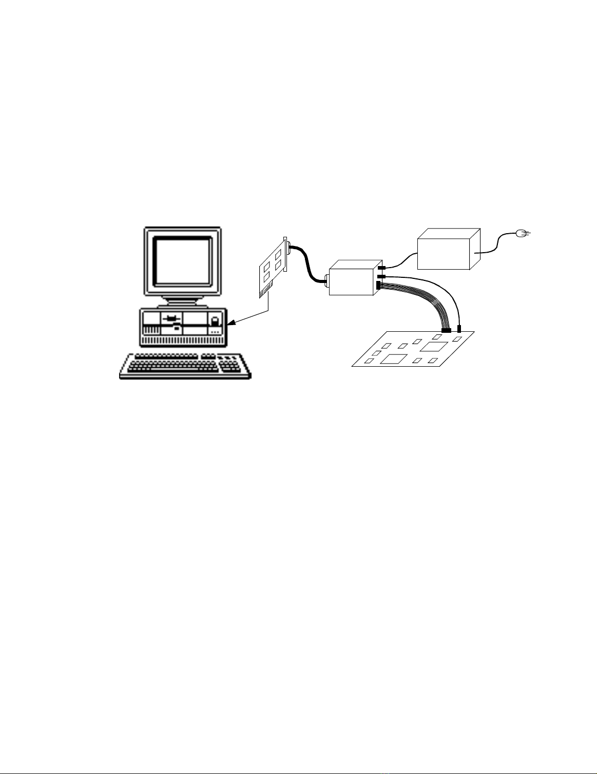
Information Manual DSP1611/17/18/27/28/29 DIGITAL SIGNAL PROCESSOR
April 1998 Introduction
1.3 Application Support (continued)
1.3.2 Hardware Development System
(continued)
Figure 1-1 shows the components of the DSP1600 hardware development system for in-circuit emulation. The PC
is an
MS-DOS
386, 486-based, or better machine. The enhanced system controller card (ESCC) plugs into an
8-bit slot on the PC ISA I/O bus and connects to the enhanced target interface box (ETIB). The ETIB provides a
JTAG interface to the target DSP1611/17/18/27/28/29 device using a 9-pin connector cable. With this configuration, a program can be downloaded into the DSP on the user's board and executed at full speed. The emulation is
performed with the actual DSP located on the user's board, and not one separated from it by a performancelimiting cable. Program development with breakpointing, single-stepping, and branch tracing is available with the
simulator; it is aided by the hardware development system module on the DSP1611/17/18/27/28/29.
ESCC
ESCC – ENHANCED SYSTEM CONTROLLER CARD
ETIB – ENHANCED TARGET INTERFACE BOX
37-PIN CABLE
ETIB
9-PIN CABLE
(JTAG INTERFACE)
TARGET BOARD
POWER
SUPPLY
ac SUPPLY
TARGET BOARD
POWER CABLE
(12.0 V —15.0 V)
Figure 1-1. In-Circuit Emulation with the
FlashDSP
1600—JCS
Another development tool available is the demonstration board (DSP1611/17/18/27/28/29-DEMO). The demonstration board replaces the customer board in Figure 1-1 and provides a development platform with external memory (static RAM or PROM), a DSP1611/17/18/27/28/29 device, and access many DSP signals.
Lucent Technologies Inc.
DRAFT COPY
1-5
Page 25

DSP1611/17/18/27/28/29 DIGITAL SIGNAL PROCESSOR Information Manual
Introduction April 1998
1.4 Manual Organization
This document is a ref erence guide for the DSP1611, DSP1617, DSP1618, DSP1627, DSP1628, and DSP1629. It
describes the architecture, instruction set, and interfacing requirements of the device. The remaining chapters of
this manual are outlined below:
Chapter 2.
Hardware Architecture
ing the major elements of the architecture and how they function.
: An overall description of the device including separate sections describ-
Chapter 3.
Chapter 4.
Chapter 5.
Chapter 6.
Chapter 7.
Chapter 8.
Chapter 9.
Chapter 10.
Chapter 11.
Chapter 12.
Chapter 13.
Chapter 14.
Software Architecture
Included are a register view of the chip, arithmetic and precision of data, memory space description, and the interrupt structure.
Instruction Set
Notation and addressing modes are also discussed in detail. Appendix B lists the complete
instruction set and provides a description of each instruction including r estrictions and normal
uses.
Core Architecture
External Memory Interface
Serial I/O
clocking, interrupts, and multiprocessor operation.
Parallel I/O (DSP1617 Only)
interrupt information.
Parallel Host Interface (PHIF) (DSP1611/18/27/28/29 Only)
ation of this port, including interrupt information.
Bit I/O Unit
JTAG Test Access Port
Timer
: Operation and programming.
Bit Manipulation Unit
Error Correction Coprocessor (DSP1618/28 Only)
: This section describes the general characteristics of the groups of instructions.
: A detailed analysis of the operation of the serial I/O ports including active and passive
: A functional description of the operation and programming of this port.
: A description of the topics associated with the software of the device.
: A detailed description of the DSP1600 core architecture.
: A description of the EMI port including functional timing.
: A detailed analysis of the operation of this parallel I/O port including
: A functional description of the oper-
: Functional description of the JTAG port.
: A detailed description of the bit manipulation unit.
: A detailed description of this coprocessor.
Chapter 15.
Appendix A.
Appendix B.
1-6
Interface Guide
Instruction Encoding
Instruction Set Summary
: A functional description of each category of pins with tables describing pins.
: Lists the hardware-level encoding of the instruction set.
: Each instruction is described in detail.
DRAFT COPY
Lucent Technologies Inc.
Page 26

Information Manual DSP1611/17/18/27/28/29 DIGITAL SIGNAL PROCESSOR
April 1998 Introduction
1.4 Manual Organization (continued)
1.4.1 Applicable Documentation
A variety of documents exists to provide specific information on various members of the DSP1600 product family.
Contact your Lucent Technologies Account Manager for the latest issue of any of the following documents. The
back cover lists contact numbers for customer assistance.
DSP1611/17/18/27/28/29 Digital Signal Processor Information Manual (this manual) is a reference guide for the
DSP1611/17/18/27/28/29. It describes the architecture, instruction set, and interfacing requirements.
DSP1611, DSP1617, DSP1618, DSP1627, DSP1628, and DSP1629 Digital Signal Processor data sheets provide
up-to-date timing requirements and specifications, electrical characteristics, and a summary of the instruction set
and device architecture for each device.
DSP1600 Support Tools Manual
includes the appropriate DSP1611/17/18/27/28/29 supplement that provides the inform ation necessary to install
and use the DSP1611/17/18/27/28/29 support software. The suppor t tools manual is also required if working with
the DSP1600 Hardware Development System because the support software provides an interface between the
host computer and the development system. Each hardware development tool is packed with a user manual and
schematics.
is an online document shipped with DSP1611/17/18/27/28/29 software tools. It
Lucent Technologies Inc.
DRAFT COPY
1-7
Page 27

Chapter 2
Hardware Archite ct ure
Page 28

CHAPTER 2. HARDWARE ARCHITECTURE
CONTENTS
➤ 2 Hardware Architecture .................................................................................................................................2-1
➤ 2.1 Device Architecture Overview............................................................................................................2-1
➤ 2.1.1 Harvard Architecture ...........................................................................................................2-1
➤ 2.1.2 Concurrent Operations ................................................................................................... .....2-2
➤ 2.1.3 Device Architecture .............................................................................................................2-4
➤ 2.1.4 Memory Spac e and Bank Switching .................................................................................2-12
➤ 2.1.5 Internal Instruction Pipeline ..............................................................................................2-13
➤ 2.2 Core Architecture Overview.............................................................................................................2-16
➤ 2.2.1 Data Arithmetic Unit ..........................................................................................................2-16
➤ 2.2.2 Y Space Address Arithmetic Unit (YAAU) .........................................................................2-17
➤ 2.2.3 X Space Address Arithmetic Unit (XAAU) .........................................................................2-18
➤ 2.2.4 Cache ...............................................................................................................................2-18
➤ 2.2.5 Control ..............................................................................................................................2-18
➤ 2.3 Internal Memori es............................................................................................................................ 2-19
➤ 2.4 External Memory Interface (EMI).....................................................................................................2-19
➤ 2.5 Bit Manipulation Unit (BMU) ............................................................................................................2-20
➤ 2.6 Serial Input/Output (SIO) Units........................................................................................................2-20
➤ 2.7 Parallel Input/Output (PIO) (DSP1617 Only) ...................................................................................2-21
➤ 2.8 Parallel Host Interface (PHIF) (DSP1611/18/27/28/29 Only)...........................................................2-21
➤ 2.9 Bit Input/Output (BIO) ......................................................................................................................2-22
➤ 2.10 JTAG................................................................................................................................................2-22
➤ 2.11 Timer................................................................................................................................................2-22
➤ 2.12 Hardware Development System (HDS) Module...............................................................................2-23
➤ 2.13 Clock Synthesis (DSP1627/28/29 Only)..........................................................................................2-23
➤ 2.14 Power Management.........................................................................................................................2-23
Page 29
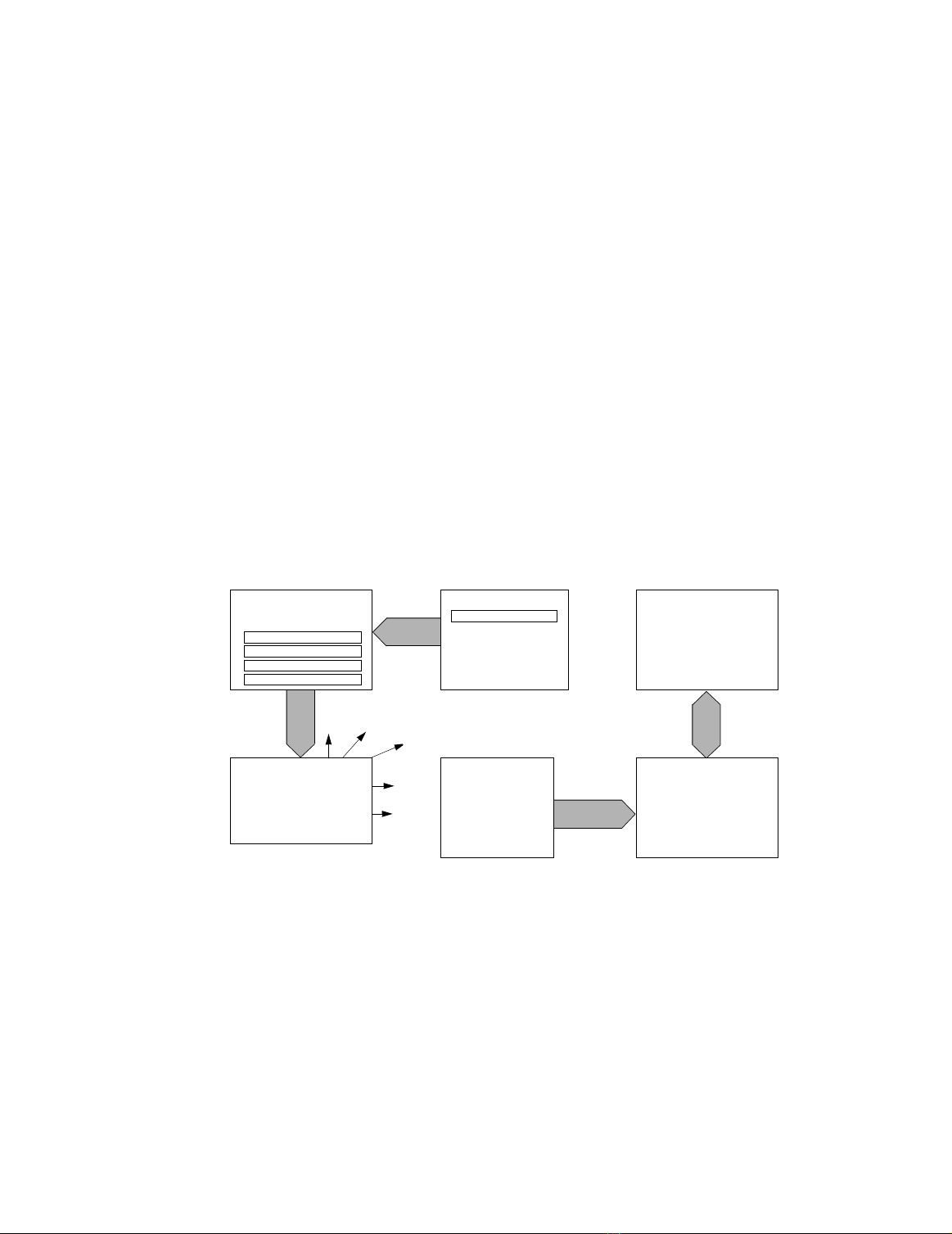
Information Manual DSP1611/17/18/27/28/29 DIGITAL SIGNAL PROCESSOR
April 1998
2 Hardware Architecture
This chapter presents an overview of the hardware in the DSP1611, DSP1617, DSP1618, DSP1627, DSP1628,
and DSP1629. First, an overall view of the architecture is discussed; then, each major functional block is
described. The following chapters give full details on each block.
2.1 Device Architecture Overview
2.1.1 Harvard Architecture
Figure 2-1 shows a view of a simple operation in the DSP1611/17/18/27/28/29 architecture to demonstrate funda-
mentally how an instruction is processed. The architecture is a Harvard architecture defined as having two separate memory spaces. The first is the instruction/coefficient space or program space that is referred to in this
manual as the X-memory space. The second is the data memory space that is referred to as the Y-memor y
space. Each memory space has a corresponding address arithmetic unit. In the instruction/coefficient memory
space, the progr am addr essi ng unit (XAAU) places addresses on the program address bus (XAB). In this example ,
these addresses go to the internal ROM that, then, places instructions on the program data bus (XDB). The
instructions are decoded in the control block that, in turn, provides control signals to all of the processor sections.
The control signals respond to instructions that, in this example, call for arithmetic operations on data residing in
the RAM. The data addressing unit (YAAU) addresses the RAM over the data address bus (YAB), and data is
transferred between the RAM and data arithmetic unit (DAU) over the data bus (YDB). The power of the architecture lies in the parallel operations that are possible. In this case, instruction processing, data transfer, and arithmetic operations can all be done simultaneously.
ROM
INSTRUCTIONS
16
CONTROL
XAB
16
PROG. COUNTER
PROGRAM
ADDRESS
UNIT
DATA
ADDRESS
UNIT
YAB
16
Figure 2-1. Harvard Architecture
DATA
ARITHMETIC
UNIT
16
YDBXDB
RAM
5-4140
Lucent Technologies Inc.
DRAFT COPY
2-1
Page 30
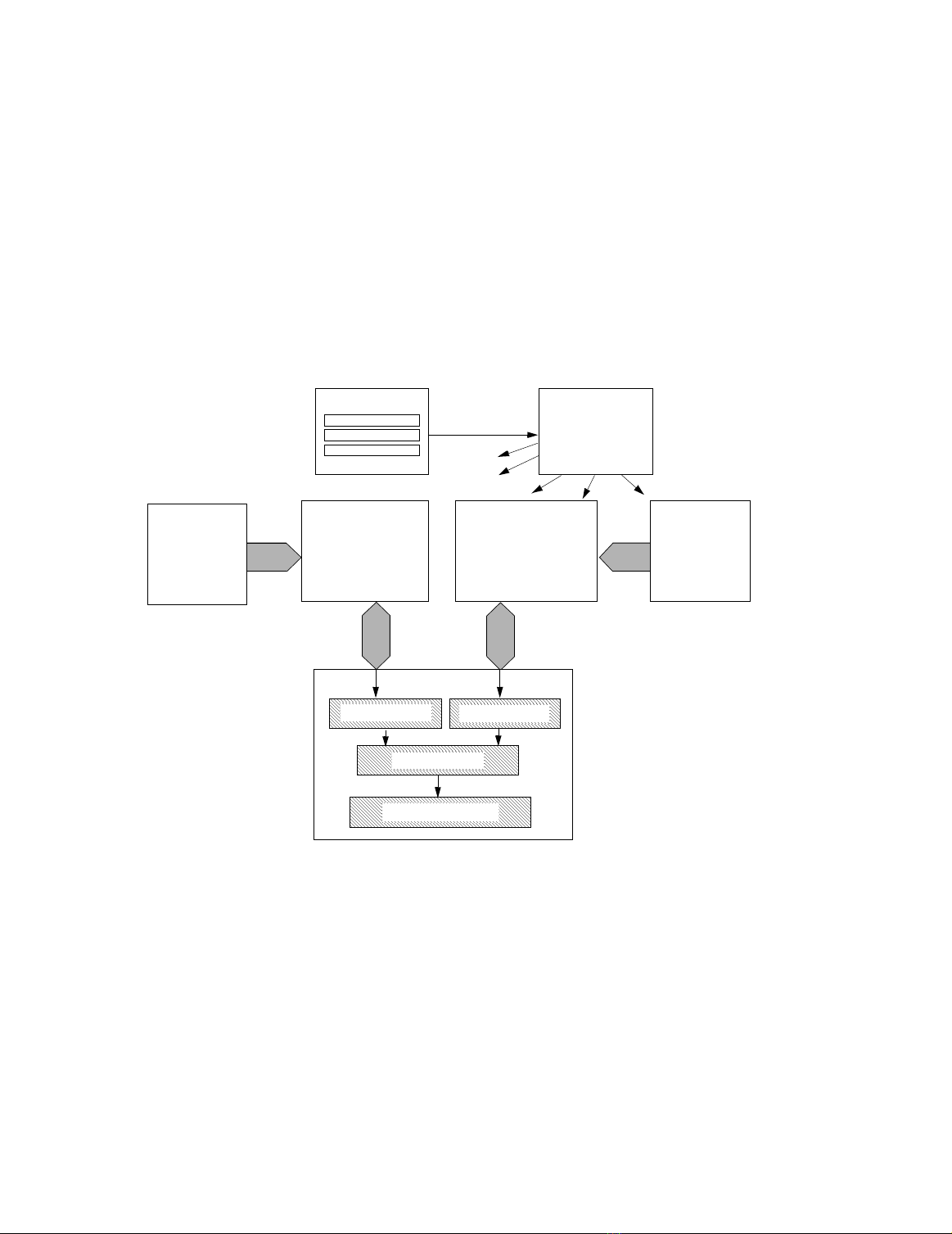
DSP1611/17/18/27/28/29 DIGITAL SIGNAL PROCESSOR Information Manual
Hardware Architecture April 1998
2.1 Device Architecture Overview (continued)
2.1.2 Concurrent Operations
Figure 2-2 shows the hardware view of an example of concurrent operations in the de vice. It also demonstrates the
flexibility of the memory spaces. In this example, the progr am is e x ecuti ng from the instruction cache. Instructions
are fed directly to the contr ol section freeing the XAB. The program addressing unit (XAAU) is now addressing one
bank of the dual-port RAM (Bank 1) to transfer variable coefficients between the RAM and the DAU. It could alternatively have been addressing the ROM to transf er fixed coefficients to the DAU . The data addressing unit (YAAU)
is addressing another bank of the dual-port RAM (Bank 4) to transfer data between the RAM and the DAU. Thus,
in one instruction cycle, two words of data can be transferred to the DAU simultaneously during internal calculations in the DAU. In the DAU, a multiplication can occur at the same time as an accumulation of a previous
product. In fact, a multiplication can occur in parallel w i th a variety of ALU operations.
YAAU
YAB
DAU
CACHE
INSTRUCTIONS
DUAL-PORT
RAM
BANK 1
DATA
y REGISTER
YDB
MULTIPLIER
ACCUMULATOR
INTERNAL
BUS
DUAL-PORT
XDB
x REGISTER
RAM
BANK 4
VARIABLE
COEFFICIENTS
CONTROL
XAB
XAAU
5-4141.a
2-2
Figure 2-2. Concurrent Operations in the DSP1611/17/18/27/28/29
DRAFT COPY
Lucent Technologies Inc.
Page 31

Information Manual DSP1611/17/18/27/28/29 DIGITAL SIGNAL PROCESSOR
April 1998 Hardware Architecture
2.1 Device Architecture Overview (continued)
2.1.2 Concurrent Operations
(continued)
Table 2-1 shows the sequence of instructions whose operations are described in the previous example. The pipe-
lining of functional operations and data transfers is illustrated. The interpretation of the instructions is as follows:
y
= Y means place the contents of memory space Y in register y. In the actual instruction, Y could be replaced by
*rM++. *rM++ denotes the memory location pointed to by the address in register rM (M = <0—3>) and postincrement the address. Similarly, x = X means place the contents of memory space X in register x. In the actual
instruction, X could be replaced by *pt++. *pt++ denotes the memory location pointed to by the address in the pt
register and postincrement the address.p =
register p.
a0 = a0 + p
means add the value in p to the previous value in accumulator a0. The subscripts are
x*y
means multiply the data in registers x and y and put the result in
attached to indicate the order of the operation and to demonstrate the flow of the results of operations on y and x.
In this example, an accumulation takes place during every instruction cycle b ut there is a delay of three instructions
from the data into the x and y registers to the final accumulation.
Ta ble 2-1. Pipeline Flow for Concurrent Operations
Instruction # Accumulator Multiplier Registers
(1) a0
0
= a0–1 + p
(2) a01 = a00 + p
(3) a02 = a01 + p
0
1
2
1
p1 = x
*
p2 = x2 * y
3
p3 = x
*
1
y
2
3
y
y2 = Y2, x2 = X
y3 = Y3, x3 = X
y4 = Y4, x4 = X
2
3
4
The most efficient programs use the parallelism as described above to the fullest extent. The instructions that
allow concurrent operations are the multiply/A LU instructions with their associated data transf ers and are described
in detail in Chapter 4, Instruction Set.
Lucent Technologies Inc.
DRAFT COPY
2-3
Page 32

DSP1611/17/18/27/28/29 DIGITAL SIGNAL PROCESSOR Information Manual
Hardware Architecture April 1998
2.1 Device Architecture Overview (continued)
2.1.3 Device Architecture
Figures 2-3, 2-4, 2-5, 2-6, 2-7, and 2-8 show the block diagrams for DSP1611, DSP1617, DSP1618, DSP1627,
DSP1628, and DSP1629 processors. The major blocks are the DSP1600 processor core, the memories, the bit
manipulation unit, the external memory interface, the serial input(s)/output(s ), the parallel input/output, the bit I/O,
the JTAG, and the timer.
CKI
CKI2
CKO
RSTB
STOP
TRAP
INT[1:0]
IACK
VEC[3:0] OR IO BI T [ 7: 4]
DO2 OR PS EL1
OLD2 OR PO D S
OCK2 OR PS EL2
OBE2 OR POBE
SYNC2 OR PSEL0
ICK2 OR PB0
ILD2 OR PIDS
DI2 OR PB1
IBF2 OR PI BF
DOEN2 OR PB2
SADD2 OR PB3
IOBIT[3:0] OR PB[7:4]
AB[15:0]DB[15:0]
ioc
DUAL-PORT
RAM
12K x 16
M
U
X
RWN EXM DSEL EROM ERAMHI
EXTERNAL MEMORY INTERFACE & EMUX
YAB YDB XDB XAB BMU
DSP1600 CORE
PHIF
phifc
†
PSTAT
pdx0(IN)
pdx0(OUT)
I/O
IDB
powerc
BIO
sbit
cbit
ROM
1K x 16
aa0
aa1
ar0
ar1
ar2
ar3
ERAMLO
SIO2
sdx2(OUT)
srta2
tdms2
sdx2(IN)
sioc2
saddx2
JTAG
BOUNDARY-SCAN
jtag
†
JCON
†
ID
†
BYPASS
HDS
BREAKPOINT
TRACE
†
†
TIMER
timerc
timer0
SIO1
sdx(OUT)
srta
tdms
sdx(IN)
sioc
saddx
TDO
TDI
TCK
TMS
DI1
ICK1
ILD1
IBF1
DO1
OCK1
OLD1
OBE1
SYNC1
SADD1
DOEN1
† These registers are acce ssible through ex t ernal pi ns only.
Figure 2-3. DSP1611 Block Diagram
2-4
DRAFT COPY
5-4142.a
Lucent Technologies Inc.
Page 33

Information Manual DSP1611/17/18/27/28/29 DIGITAL SIGNAL PROCESSOR
April 1998 Hardware Architecture
2.1 Device Architecture Overview (continued)
2.1.3 Device Architecture
DUAL-PORT
CKI
CKI2
CKO
RSTB
STOP
TRAP
INT[1:0]
IACK
VEC[3:0] OR IOBIT[7:4]
DO2 OR PSE L1
OLD2 OR PODS
OCK2 OR PSEL2
OBE2 OR POBE
SYNC2 OR PSEL0
ICK2 OR PB0
ILD2 OR PIDS
DI2 OR PB1
IBF2 OR PIBF
DOEN2 OR PB2
SADD2 OR PB3
IOBIT[3:0] OR PB[7:4]
(continued)
ioc
RAM
4K x 16
M
U
X
RWN EXM DSEL EROM ERAMHIAB[15:0]DB[15:0] I/O ERAMLO
EXTERNAL MEMORY INTERFACE & EMUX
ROM
24K x 16
YAB YDB XDB XAB BMU
DSP1600 CORE
IDB
PIO
pioc
†
PSTAT
pdx<0—7>(IN)
pdx<0—7>(OUT)
powerc
BIO
sbit
cbit
aa0
aa1
ar0
ar1
ar2
ar3
SIO2
sdx2(OUT)
srta2
tdms2
sdx2(IN)
sioc2
saddx2
JTAG
BOUNDARY-SCAN
jtag
†
JCON
†
ID
†
BYPASS
HDS
BREAKPOINT
TRACE
TIMER
†
†
timerc
timer0
SIO1
sdx(OUT)
srta
tdms
sdx(IN)
sioc
saddx
TDO
TDI
TCK
TMS
DI1
ICK1
ILD1
IBF1
DO1
OCK1
OLD1
OBE1
SYNC1
SADD1
DOEN1
†These registers are accessible through external pins only.
Figure 2-4. DSP1617 Block Diagram
Lucent Technologies Inc.
DRAFT COPY
5-4142.b
2-5
Page 34

DSP1611/17/18/27/28/29 DIGITAL SIGNAL PROCESSOR Information Manual
Hardware Architecture April 1998
2.1 Device Architecture Overview (continued)
2.1.3 Device Architecture
CKI
CKI2
CKO
RSTB
STOP
TRAP
INT[1:0]
IACK
VEC[3:0] OR I OBIT[7:4]
DO2 OR PS EL1
OLD2 OR PO D S
OCK2 OR PS EL2
OBE2 OR PO BE
SYNC2 OR PSEL0
ICK2 OR PB0
ILD2 OR PIDS
DI2 OR PB1
IBF2 OR PI BF
DOEN2 OR PB2
SADD2 OR PB3
IOBIT[3:0] OR PB[7:4]
(continued)
AB[15:0]DB[15:0]
ioc
‡
ROM
16K x 16
DUAL-PORT
RAM[3:1]
3K x 16
M
U
X
powerc
I/O
IDB
BIO
sbit
cbit
RAM4
1K x 16
ECCP
eir
ear
edr
aa0
aa1
ar0
ar1
ar2
ar3
RWN EXM DSEL EROM ER AM H I
EXTERNAL MEMORY INTERFACE & E MUX
YAB YDB XDB XAB BMU
DSP1600 C OR E
PHIF
phifc
†
PSTAT
pdx0(IN)
pdx0(OUT)
ERAMLO
SIO2
sdx2(OUT)
srta2
tdms2
sdx2(IN)
sioc2
saddx2
JTAG
BOUNDARY-SCAN
jtag
†
JCON
†
ID
†
BYPASS
HDS
BREAKPOINT
TRACE
TIMER
†
†
timerc
timer0
SIO1
sdx(OUT)
srta
tdms
sdx(IN)
sioc
saddx
TDO
TDI
TCK
TMS
DI1
ICK1
ILD1
IBF1
DO1
OCK1
OLD1
OBE1
SYNC1
SADD1
DOEN1
† These registers are acce ssible through ex t ernal pi ns only.
‡ DSP1618x24 contains 24K x 16 ROM .
Figure 2-5. DSP1618 Block Diagram
2-6
DRAFT COPY
5-4142.c
Lucent Technologies Inc.
Page 35

Information Manual DSP1611/17/18/27/28/29 DIGITAL SIGNAL PROCESSOR
April 1998 Hardware Architecture
2.1 Device Architecture Overview (continued)
2.1.3 Device Architecture
DUAL-PORT
CKI
CKI2
CKO
RSTB
STOP
TRAP
INT[1:0]
IACK
VEC[3:0] OR IO BI T [ 7: 4]
DO2 OR PS EL1
OLD2 OR PO D S
OCK2 OR PS EL2
OBE2 OR POBE
SYNC2 OR PSEL0
ICK2 OR PB0
ILD2 OR PIDS
DI2 OR PB1
IBF2 OR PI BF
DOEN2 OR PB2
SADD2 OR PB3
IOBIT[3:0] OR PB[7:4]
M
U
X
(continued)
AB[15:0]DB[15:0]
ioc
RAM
6K x 16
PSTAT
pdx0(IN)
pdx0(OUT)
powerc
I/O
IDB
CLOCK
SYNTHESIZER
BIO
sbit
cbit
RWN EXM EROM ERAMHI
EXTERNAL MEMORY INTERFACE & EMUX
YAB YDB XDB XAB BMU
DSP1600 CORE
PHIF
phifc
†
pllc
ERAMLO
ROM
36K x 16
aa0
aa1
ar0
ar1
ar2
ar3
‡
sdx2(OUT)
SIO2
srta2
tdms2
sdx2(IN)
sioc2
saddx2
JTAG
BOUNDARY-SCAN
jtag
†
JCON
†
ID
†
BYPASS
HDS
BREAKPOINT
TRACE
sdx(OUT)
†
†
TIMER
timerc
timer0
SIO1
srta
tdms
sdx(IN)
sioc
saddx
TDO
TDI
TCK
TMS
DI1
ICK1
ILD1
IBF1
DO1
OCK1
OLD1
OBE1
SYNC1
SADD1
DOEN1
†These registers are accessible through external pins only.
‡DSP1627x32 contains 32K x 16 in ternal ROM.
Figure 2-6. DSP1627 Block Diagram
Lucent Technologies Inc.
DRAFT COPY
5-4142.d
2-7
Page 36

DSP1611/17/18/27/28/29 DIGITAL SIGNAL PROCESSOR Information Manual
Hardware Architecture April 1998
2.1 Device Architecture Overview (continued)
2.1.3 Device Architecture
CKI
CKI2
CKO
RSTB
STOP
TRAP
INT[1:0]
IACK
VEC[3:0] OR I OBIT[7:4]
DO2 OR PS T AT
OLD2 OR PO D S
OCK2 OR PCSN
OBE2 OR PO BE
SYNC2 OR PBSEL
ICK2 OR PB0
ILD2 OR PIDS
DI2 OR PB1
IBF2 OR PI BF
DOEN2 OR PB2
SADD2 OR PB3
IOBIT[3:0] OR PB[7:4]
(continued)
AB[15:0]DB[15:0]
ioc
ROM
48K x 16
DUAL-PORT
‡
RAM
15/7K x 16
M
U
X
RWN EXM DSEL EROM ER AM H I
EXTERNAL MEMORY INTERFACE & E MUX
XAB XDB YAB YDB BMU
DSP1600 C OR E
PHIF
phifc
†
PSTAT
pdx0(IN)
pdx0(OUT)
powerc
I/O
IDB
BIO
sbit
cbit
RAM4
1K x 16
ECCP
eir
ear
edr
CLOCK
SYNTHESIZER
pllc
‡
aa0
aa1
ar0
ar1
ar2
ar3
ERAMLO
SIO2
sdx2(OUT)
srta2
tdms2
sdx2(IN)
sioc2
saddx2
JTAG
BOUNDARY-SCAN
jtag
†
JCON
†
ID
†
BYPASS
HDS
BREAKPOINT
TRACE
TIMER
†
†
timerc
timer0
SIO1
sdx(OUT)
srta
tdms
sdx(IN)
sioc
saddx
TDO
TDI
TCK
TMS
TRST
DI1
ICK1
ILD1
IBF1
DO1
OCK1
OLD1
OBE1
SYNC1
SADD1
DOEN1
† These registers are acce ssible through ex t ernal pi ns only.
‡ DSP1628x16 contains a total of 16K x 16 internal RAM, and DSP1628x08 contains a total of 8K x 16 internal RAM.
Figure 2-7. DSP1628 Block Diagram
2-8
DRAFT COPY
Lucent Technologies Inc.
Page 37

Information Manual DSP1611/17/18/27/28/29 DIGITAL SIGNAL PROCESSOR
April 1998 Hardware Architecture
2.1 Device Architecture Overview (continued)
2.1.3 Device Architecture
DUAL-PORT
16K/10K x 16
CKI
CKI2
CKO
RSTB
STOP
TRAP
INT[1:0]
IACK
VEC[3:0] OR IO BI T [ 7: 4]
DO2 OR PS T AT
OLD2 OR PO D S
OCK2 OR PCSN
OBE2 OR POBE
SYNC2 OR PBSEL
ICK2 OR PB0
ILD2 OR PIDS
DI2 OR PB1
IBF2 OR PI BF
DOEN2 OR PB2
SADD2 OR PB3
IOBIT[3:0] OR PB[7:4]
M
U
X
(continued)
AB[15:0]DB[15:0] I/O
ioc
RAM
RWN EXM EROM ERAMHI
EXTERNAL MEMORY INTERFACE & EMUX
‡
YAB YDB XDB XAB BMU
DSP1600 CORE
PHIF
phifc
†
PSTAT
pdx0(IN)
pdx0(OUT)
powerc
IDB
BIO
sbit
cbit
48K x 16
aa0
aa1
ar0
ar1
ar2
ar3
CLOCK
SYNTHESIZER
pllc
ROM
ERAMLO
sdx2(OUT)
sdx2(IN)
SIO2
srta2
tdms2
sioc2
saddx2
JTAG
BOUNDARY-SCAN
jtag
†
JCON
†
ID
†
BYPASS
HDS
BREAKPOINT
TRACE
sdx(OUT)
†
†
TIMER
timerc
timer0
SIO1
srta
tdms
sdx(IN)
sioc
saddx
TDO
TDI
TCK
TMS
TRST
DI1
ICK1
ILD1
IBF1
DO1
OCK1
OLD1
OBE1
SYNC1
SADD1
DOEN1
†These registers are accessible through external pins only.
‡DSP1629x16 contains 16K x 16 in ternal RAM, and DSP1629x10 contains 16K x 10 internal RAM.
Figure 2-8. DSP1629 Block Diagram
Lucent Technologies Inc.
DRAFT COPY
2-9
Page 38

DSP1611/17/18/27/28/29 DIGITAL SIGNAL PROCESSOR Information Manual
Hardware Architecture April 1998
2.1 Device Architecture Overview (continued)
2.1.3 Device Architecture
Table 2-2. Symbols Used in the Block Diagrams
Symbol Name/Description
aa0—aa1 Alternate Accumulators
ar0—ar3 Auxiliary BMU Registers
BIO Bit Input/Output Unit
BMU Bit Manipulation Unit
BREAKPOINT Four Instruction Breakpoint Registers
BYPASS JTAG Bypass Register
cbit Control Register for BIO
ECCP Error Correction Coprocessor (DSP1618 and DSP1628 only)
ear ECCP Address Register (DSP1618 and DSP1628 only)
edr ECCP Data Register (DSP1618 and DSP1628 only)
eir ECCP Instruction Register (DSP1618 and DSP1628 only)
EMUX External Memory Multiplexor
HDS Hardware Development System
ID JTAG Device Identification Register
IDB Internal Data Bus
ioc I/O Configuration Register
JCON JTAG Configuration Register
JTAG Standardized Test Port Defined in
jtag 16-bit Serial/Parallel Register
pdx0—pdx7(IN) Parallel I/O Data Transmit Input Registers <0—7>
pdx0—pdx7(OUT) Parallel I/O Data Transmit Output Registers <0—7>
PHIF Parallel Host Interface (DSP1611/18/27/28/29 only)
phifc Parallel Host Interface Control Register (DSP1611/18/27/28/29 only)
pllc Phase-lock Loop C ontrol Register (DSP1627/28/29 only)
PIO Parallel Input/Output Unit (DSP1617 only)
pioc Parallel I/O Control Register (DSP1617 only)
powerc Power Control Register
PSTAT Parallel I/O Status Register
ROM Internal ROM (1 Kword for DSP1611, 24 Kwords for D SP1617, 16 Kwords
saddx Multiprocessor Protocol Register
sbit Status Register for BIO
sdx(IN) Serial Data Transmit Input Register
sdx2(IN) Serial Data Transmit Input Register for SIO2
sdx(OUT) Serial Data Transmit Output Register
sdx2(OUT) Serial Data Transmit Output Register for SIO2
SIO1 Serial Input/Output Unit #1
SIO2 Serial Input/Output Unit #2
(continued)
IEEE
P1149.1
for DSP1618, 24 Kwords for DSP1618x24, 36 Kwords for DSP1627,
32 Kwords for DSP1627x32, 48 Kwords for DSP1628 and DS P1629)
2-10
DRAFT COPY
Lucent Technologies Inc.
Page 39

Information Manual DSP1611/17/18/27/28/29 DIGITAL SIGNAL PROCESSOR
April 1998 Hardware Architecture
2.1 Device Architecture Overview (continued)
2.1.3 Device Architecture
Table 2-2. Symbols Used in the Block Diagrams
Symbol Name/Description
sioc Serial I/O Control Register
sioc2 Serial I/O Control Register for SIO2
srta<1, 2> Serial Receive/Transmit Address Registers
tdms<1, 2> Seri al I/O T ime-division Multiplex Signal Control Registers
TIMER Programmable Timer
timer0 Time Running Count Register
timerc Timer Control Register
TRACE Program Discontinuity
XAB Program Space Address Bus
XDB Program Space Data Bus
YAB Data Space Address Bus
YDB Data Space Data Bus
DUAL-PORT RAM Internal dual-port R AM (12 Kwords for DSP1611, 4 Kwords for DSP1617
(continued)
(continued)
and DSP1618, 6 Kwords for DSP1627, 8 Kw ords for DSP1628x08,
16 Kwords for DSP1628x16, 10 Kwords f or DSP1629x10, and 16 Kwords for
DSP1629x16)
Lucent Technologies Inc.
DRAFT COPY
2-11
Page 40

DSP1611/17/18/27/28/29 DIGITAL SIGNAL PROCESSOR Information Manual
Hardware Architecture April 1998
2.1 Device Architecture Overview (continued)
2.1.4 Memory Space and Bank Switching
Table 2-3 describes the two memory spaces.
Table 2-3. Memor y Space
Terminology Address
Data (Y) memory space (see Section
3.2.1).
Source
YAAU YAB RAM[1:x]
Address
Bus
Memory Segments
Accessed
†
IO
Data Bus
YDB
ERAMLO
ERAMHI
Program or instruction/coefficient (X)
memory space (see Section 3.2.2).
XAAU XAB [RAM1:x]
IROM
†
XDB
EROM
† x = 4 for DSP1617 and DSP1618.
x = 6 for DSP1627.
x = 8 for DSP1628x08.
x = 10 for DSP1629x10.
x = 12 for DSP1611.
x = 16 for DSP1628x16 and DSP1629x16.
There are two memory spaces with separate addressing units, address buses, and data buses. The actual memories associated with the spaces are enabled automatically based on the address. For the data memory space,
either internal dual-port RAM or external memory is used. The external memory is divided into three segments.
The internal dual-port RAM is divided into multiple 1K word banks for DSP1611/17/18/27/28/29. For the program
memory space, either internal ROM, internal dual-port RAM, or external ROM can be addressed. There are
16
= 65,536 addresses in each of the two memory spaces; the total address space for each is divided into seg-
2
ments, and each segment is associated with a physical memor y. The arrangement of the segments is called the
memory map. There is one map for the data memory space, and there are four possible memory maps for the program space. Memory maps are discussed in Section 3.2, Memory Space and Addressing and Section 6.1, EMI
Function.
2-12
DRAFT COPY
Lucent Technologies Inc.
Page 41

Information Manual DSP1611/17/18/27/28/29 DIGITAL SIGNAL PROCESSOR
April 1998 Hardware Architecture
2.1 Device Architecture Overview (continued)
2.1.4 Memory Space and Bank Switching
(continued)
The internal dual-port RAM can be accessed in both the Y space and the X space. This RAM is arranged in multi-
ple 1 Kword banks; and as long as the banks accessed are different, simultaneous data and instruction accesses
can be made. If the same bank is accessed from both memory spaces simultaneously, an extra instruction cycle
(one wait-state) is automatically initiated to carry out the transfer. The data transfer is performed first.
It is important to note that the selection of physical memory within a memory space is automatic because it only
depends on choice of address, and no ex tra time is involved to switch banks except in the case of accessing the
same bank of internal RAM just described.
2.1.5 Internal Instruction Pipeline
The internal pipeline of fetch, decode, and execute is hidden from the user. The latencies involved are automati-
cally controlled without external intervention. The following is pr o vided f or information only. The relevant hardware
is shown in Figure 2-9.
X SPACE MEM.
INSTRUCTIONS
XDB
16
XAB
16
PC
XAAU
YDB
DAU
16
CONTROL
DAU
DECODE
AAU
DECODE
YAAU
YAB
16
Figure 2-9. Hardware Block Diagram for Internal Pipeline
RAM
5-4143
Lucent Technologies Inc.
DRAFT COPY
2-13
Page 42

DSP1611/17/18/27/28/29 DIGITAL SIGNAL PROCESSOR Information Manual
Hardware Architecture April 1998
2.1 Device Architecture Overview (continued)
2.1.5 Internal Instruction Pipeline
(continued)
Table 2-4 illustrates the internal pipeline for single-cycle instructions such as a multiply-ALU instruction involving a
read from RAM to the DAU. Each instruction cycle corresponds to one cycle of the non-wait-stated CKO. The
instructions shown on the XAB bus will appear one phase (1⁄2 an instruction cycle) later on the external memory
address bus.
Ta ble 2-4. Single-Cycle Instruction Internal Pipeline
Instruction
Cycle
11
10——instr
2 1 xaddr
20——
3 1 xaddr
30——instr
4 1 xaddr
40——instr
CKO
Level
XAB XDB AAU
DECODE
xaddr
1
2
instr
instr
0
1
instr
3
4
instr
instr
2
3
DAU
YAB YDB
DECODE
—instr–1yaddr
0
instr
–1
— data
—instr0yaddr
0
—
1
2
instr
instr
instr
1
1
— data
yaddr
— data
—instr2yaddr
3
instr
2
—
–1
0
1
2
—
—
—
—
data
–2
–1
0
1
The following describes the actions associated with each of the steps shown in bold in Table 2-4.
Instruction
Cycle
1 1 The program counter (PC) places
CKO
Level
Process Description
xaddr
1
on the address bus XA B to prog ram memory
(X space memory).
1 0 The program memory is accessed.
instr
1
2 1 The program memory responds by placing
on the instruction data bus (XDB).
2 0 The AAU decoder decodes the instruction and sets up the YAAU to address the RAM.
yaddr
3 1 The YAAU places
instr
1
decodes
.
3 0 The decoders direct a RAM read of
1
on the address bus YAB to the RAM. Also, the DA U decoder
data
1
to the DAU.
4 1 The RAM is being accessed.
4 0 The RAM places the data on the YDB, and it is loaded into the DAU.
2-14
DRAFT COPY
Lucent Technologies Inc.
Page 43

Information Manual DSP1611/17/18/27/28/29 DIGITAL SIGNAL PROCESSOR
April 1998 Hardware Architecture
2.1 Device Architecture Overview (continued)
2.1.5 Internal Instruction Pipeline
(continued)
Table 2-5 illustrates the internal pipeline for a two-cycle fetch from X-memory space by using the pt register and a
concurrent compound read/write of the Y-memory space by using the multiply/ALU instruction:
Z : y x = *pt++
.
Ta ble 2-5. Two-Cycle Fetch Internal Pipeline
Instruction
Cycle
11
10——instr
2 1 xaddr
20——
31
30——
4 1 xaddr
40——instr
5 1 xaddr
CKO
Level
XAB XDB AAU
DECODE
xaddr
1
2
instr
instr
0
1
instr
ptaddr
instr
2
instr
3
4
coeff
instr
3
DAU
YAB YDB
DECODE
—instr–1yaddr
0
instr
–1
— data
—instr0yaddr
1
—
1
—
2
instr
instr
instr
instr
instr
0
1
1
1
1
— data
yaddr
— data0
yaddr
—
—instr2yaddr
–1
1w
—
–2
0
1r
2
—
—
data
data
—
–1
1w
1r
The following describes the actions associated with each of the steps shown in bold in Table 2-5.
Instruction
Cycle
1 1 The program counter (PC) places
CKO
Level
Process Description
xaddr
1
on the address bus XAB to program memory
(X space memory).
1 0 The program memory is accessed.
instr
2 1 The program memory responds by placing
1
on the instruction data bus (XDB).
2 0 The AAU decoder decodes the instruction, and sets up the YAAU to address the RAM
and the XAAU to place the contents of the pt register on the XAB. The control section
recognizes a two-cycle instruction.
yaddr
1r
3 1 The Y AA U places
instr
1
decodes
. The contents of the pt register (
3 0 The decoder directs a RAM read of
4 1 The data,
coeff
, from the X memor y is transferred to the x register. The
on the address bu s YAB to the RAM. Also, the D AU decoder
ptaddr
) are placed on the XAB.
data
1r
to the DAU. The RAM is accessed.
data
1w
is
transferred to the RAM from the y register.
data
1r
4 0 The
data
is transferred from the RAM to the y register. The RAM is written with
1w
.
Lucent Technologies Inc.
DRAFT COPY
2-15
Page 44

DSP1611/17/18/27/28/29 DIGITAL SIGNAL PROCESSOR Information Manual
Hardware Architecture April 1998
2.2 Core Architecture Overview
2.2.1 Data Arithmetic Unit
The data arithmetic unit (DAU) is the main execution unit for signal processing algorithms. The DAU consists of a
16-bit by 16-bit multiplier, a 36-bit ALU, and two 36-bit accumulators: a0 and a1. The DAU performs two's complement, fixed-point arithmetic and i s us abl e as a m ultiply /accumul ate or ALU structure. The DAU multipli er and adder
operate in parallel r equiring, together , one instruction cycle for their e xec ution. Microprocessor-like instructions are
executed by the ALU.
CONTROL
x (16)
16 x 16 M P Y
SHIFT (–2, 0, 1, 2)
EXTRACT/SAT
yh (16)
p (32)
ALU/SHIFT
a0 (36)
a1 (36)
16
ins (16)
inc (16)
MUX
32
yl (16)
36
CACHE
cloop ( 7)
alf (16 )
mwait (16)
DAU
c0 (8)
c1 (8)
c2 (8)
auc (16)
psw (16)
SYS
re (16)
CMP
ybase (16)
ADDER
pc (16)
pt (16)
i (16)
k (16)
ADDER
j (16)
MUX
pr (16)
pi (16)
MUX
MUX
r0 (16)
r1 (16)
r2 (16)
r3 (16)
1
XAAU
BRIDGE
–1, 0, 1, 2
rb (16)
XDB
XAB
IDB
YDB
YAAU
YAB
2-16
Figure 2-10. DSP1600 Core Functions
DRAFT COPY
5-1741.a
Lucent Technologies Inc.
Page 45

Information Manual DSP1611/17/18/27/28/29 DIGITAL SIGNAL PROCESSOR
April 1998 Hardware Architecture
2.2 Core Architecture Overview (continued)
2.2.1 Data Arithmetic Unit
multiplier
The
instruction cycle. Data for the multipl ier's inputs comes from the 16-bit x register and the upper 16 bits (high half) of
the 32-bit y register.
For multiply/ALU instructions, the x register can be loaded with coefficients from X-memory space or data from Ymemory space. The high half of the y register can be loaded from Y-memory space or the high or low half of an
accumulator. If the single-cycle square mode is set in the
loads the x register with the same data. A multiply instruction then performs a squaring function.
x, y, yl, p, pl, a0, a0l, a1
If the 32-bit registers are used in 16-bit instructions, the l suffix identifies the low half of the register and no suffix
identifies the upper half. For example, a0 means bits 31—16 of a0 and
In addition to being used as an adder in the multiply/accumulate instructions , the 36-bi t
to implement functions and algorithms in the DS P1611/17/18/27/28/29 de vice that conventionally are ex ecuted i n a
microcomputer or a microprocessor. Operands to the ALU can be data in y, p, a0, or a1, or they can be immediates. The ALU sign-extends 32-bit operands from y or p to 36 bits, and it produces a 36-bit output (32 data bits
and 4 guard bits) in one instruction cycle. Either accumulator can receive the 36-bit result. The ALU supports
dyadic (two-operand) functions including addition, subtraction, and logical AND, OR, and XOR . It also suppor ts
monadic (single-operand) functions including rounding, two's complement negation, incrementing, and left and
right shifts of 1, 4, 8, or 16 bits. More general shifting is availab le w ith the bit m anipulation uni t (see Section 2.5, Bit
Manipulation Unit (BMU)).
auc
The
of the y register and accumulators w hen the upper w ord is written. It selects or deselects saturation on overflow for
the accumulators. It selects one of four alignments of data in the p register. It controls whether the pseudorandom
sequence generator is reset if the pi register is written (see Section 5.1.6, DAU Pseudorandom Sequence Genera-
tor (PSG)). It selects the single-cycle squaring mode (See Section 5.1.2, Multiplier Functions). The
reset to all zeros at chip reset. The
provides access to the guard bits in the accumulators. The
used to count events such as the number of times the program has executed a sequence of code. They are controlled by the conditional instructions and provide a convenient method of program looping.
executes a 16-bit by 16-bit multiply and stores the 32-bit product in the product register (p) in one
(arithmetic unit control) register has five func tions . It selects or deselects clearing of the lower 16-bit word
(continued)
, and
auc
register, an instruction that loads the y register also
a1l
are also included in the general set of registers used for data mov e instructions.
a0l
means bits 15—0.
ALU
provides the capabili ty
auc
register is
psw
(processor status word) register contains flags from ALU operations and
c<0—2>
counters are 8 (signed) bits wide and can be
2.2.2 Y Space Address Arithmetic Unit (YA AU)
The YAAU supports high-speed, register-indirect data memory addressing with postmodification of the address
register. Four general-purpose 16-bit registers
Two 16-bit registers rb and re allow zero-overhead modulo addressing of data for efficient filter implementations.
Two signed registers j and k are used to hold user-defined posti ncrements. Fixed increments of +1, –1, and +2 are
also available, but the +2 increment is only available with compound addressing. Four compound-addressing
modes are provided to make read/write operations more efficient.
The Y AA U allows direct addressing of data memory . During direct addressing, the base register (
11 most significant bits of the address. The direct address instruction contains 5 bits that are concatenated with
the 11 bits in
sible registers . A data move then takes pl ace betw een the memory location specifi ed b y the 16- bit addres s and the
register selected by the DR field.
The YAAU decodes the 16-bit data memory address and provides individual enables for each 1 Kword bank of onchip dual-port RAM and three external data memory segments (ERAMHI, ERAMLO, and IO). One individual
address in the IO memory segment also has an individually decoded output DSEL
mapped I/O.
1.Not available in th e DSP1627/28 /2 9.
Lucent Technologies Inc.
ybase
to form a complete 16-bit address. The instruction also specifies one register (DR) of 16 pos-
r<0—3>
store read or write addresses for on-chip or off-chip RAM.
DRAFT COPY
ybase
) stores the
1
facilitating glueless memory-
2-17
Page 46

DSP1611/17/18/27/28/29 DIGITAL SIGNAL PROCESSOR Information Manual
Hardware Architecture April 1998
2.2 Core Architecture Overview (continued)
2.2.3 X Space Address Arithmetic Unit (XAAU)
The XAAU contains registers and an adder that control the sequencing of instructions in the processor. The program counter (PC) automatically increments through the instruction space and specifies addresses for instruction
fetches. The interrupt return register (pi) and the subroutine return register (pr) are automatically loaded with
return addresses that direct the return to main program ex ecution from inter rupt service routines and subroutines.
High-speed, register-indirect instruction/coefficient memory addressing with postincrementing is done b y using the
pt
register. The signed register i is used to hold a user-defined postincrement, or a fixed postincrement of +1 is
available.
The XAAU of the DSP1600 decodes the 16-bit instruction/coefficient address and produces enable signals for the
appropriate X-memory segment. The possible X segments are internal ROM, each 1 Kword bank of dual-port
RAM, and external ROM. The locations of these memory segments depend on which of the four memory maps is
selected (see Section 3.2, Memory Space and Addressing).
A core security mode can be selected by mask option
ries from off-chip.
2.2.4 Cache
Under user control, the on-chip cache memory can store instructions for repetitive operations to increase the
throughput and the coding efficiency of the device. The cache can store up to 15 instructions at a time and can
repeatedly cycle through those instructions up to 127 times without using user defined loop, test, and conditional
branch instructions. The set of instructions is executed as it is loaded into the cache, so zero-overhead looping is
achieved. The cache iterative count can be specified either as an immediate value at assembly time or can be
determined by the use of the
reloading the cache.
Note:
Instructions in a cache loop are noninterruptible.
cloop
register . Instructions prev iously stored i n the cache can be re-executed without
1
. This prevents reading out the contents of on-chip memo-
Cache instructions eliminate the overhead if repeating a block of instructions. Therefore, the cache reduces the
need to implement in-line coding in order to maximize the throughput. A routine using the cache uses fewer ROM
locations than an in-line coding of the same routine.
For two-operand multiply/arithmetic logic unit (ALU) instructions that do not require a write to memory, executing
from the cache decreases the execution time from two instruction cycles to one instruction cycle resulting in an
increase in throughput.
2.2.5 Control
The control block provides overall DSP1611/17/18/27/28/29 system coordination. Inputs are provided to the control block over the program data bus (XDB). The instructions are decoded by hardware in the control block. The
execution of the phases of an instruction is controlled by hardware throughout the DSP1611/17/18/27/28/29
device. The hardware sequences instructions through the pipeline and controls the I/O, the processing, the memory accesses, and the timing necessary to perform each operation.
1.The internal ROM memory of the DSP1611 is only available with a standard boot routine. DSP1611 devices do not offer the secure mask
option.
2-18
DRAFT COPY
Lucent Technologies Inc.
Page 47

Information Manual DSP1611/17/18/27/28/29 DIGITAL SIGNAL PROCESSOR
April 1998 Hardware Architecture
2.3 Internal Mem orie s
All memory (internal and external) is 16 bits wide. The DSP1611
with a variety of boot routines that make it easy for systems to download programs and data to the DSP1611’s
large internal RAM space. The DSP1617, DSP1618, DSP1627, DSP1628, and DSP1629 all feature large, maskprogrammable internal ROM memories that can be encoded with programs, fixed data, or both. The DSP1617
ROM contains 24 Kwords, the DSP1618 ROM contains 16 Kwords, the DSP1618x24 ROM contains 24 Kwords,
the DSP1627 ROM contains 36 Kwords, the DSP1627x32 ROM contains 32 Kwords, the DSP1628 contains
48 Kwords, and the DSP1629 contains 48 Kwords. The internal ROM of the code to support the hardware development system is included in ROMless devices supplied by Lucent Technologies and should be included in customer-created ROM programs.
The internal dual-port
words and has separate ports to the instruction/coefficient buses and data buses. A program can reference the
memory from either port at any time transparently and without restriction. The DSP1600 core automatically performs the multiplexing. In the event that references to both ports of a single bank are made simultaneously, the
DSP1600 core automatically performs the data port access and then inserts a wait-state followed by the instruction/coefficient port access.
A program can be downloaded from slow off-chip memory into the dual-port RAM and then executed without wait-states
coefficients are adaptive. Full-speed, remote, in-circuit emulation is possible because the dual-port RAM can be
downloaded through the JTAG port. T his download capability is also useful for self-test.
RAM
contains multiple banks of zero-wait-state memory. Each bank consists of 1K of 16-bit
. Dual-port RAM is also useful for improving the performance of convolution in cases where the
ROM
contains 1K words and is preprogrammed
2.4 External Memory Interface (EMI)
The DSP1611/17/18/27/28/29 provides a 16-bit external address bus (AB[15:0]) and a 16-bit, external, bidirectional
data bus (DB[15:0]). These buses are multiplexed between the internal instruction/coefficient memory buses (X
space) and the data memory buses (Y space). The multiplexing is automatically controlled by the core that determines the memory space to be accessed from the instruction, the memory map, and the address.
Because only Y space or X space can be accessed at one time through the EMI, a sequencer automatically handles the case when a program calls f or simultaneous access of X space and Y space. For example, if a program is
being executed from external ROM and an instruction calls for a read from external RAM, the sequencer first
accesses the X space ex ternal ROM and then reads the data from external RAM. One extra instruction cycle is
required, in addition to any external wait-states that are present if external memory is used, compared to internal
operation.
Four external memory enables (ERAMLO, IO, ERAMHI, and EROM) are outputs that control the selection of external memory segments. One of the IO addresses is individually decoded to provide an enable (DSEL
mapped I/O peripherals.
Each of the five enables can be programmed individually to delay their assertion one-half of a free-running CKO
period from the beginning of the external cycle. This allows a mix of high- and low-speed devices without bus conflicts or expensive glue logic. The DSEL
high. The ERAMLO, ERAMHI, EROM, and IO signals are active-low.
Each of the memory segments can have a different number of wait-states associated with it where a wait-state is
an extra instruction cycle inserted in the read or write cycle to allow for slower memories. The number of waitstates is programmable from 0 to 15 by setting bits in the
1.Not available in th e DSP1627/28 /2 9.
1
enable is normally active-low, but it can be programmed to be active-
mwait
register.
1
) for memory-
Lucent Technologies Inc.
DRAFT COPY
2-19
Page 48

DSP1611/17/18/27/28/29 DIGITAL SIGNAL PROCESSOR Information Manual
Hardware Architecture April 1998
2.4 External Memo ry Interface (EMI) (continued)
The DSP1611/17/18/27/28/29 allows writing to external program (X) memory. Bit 11 (WEROM) and bit 14
(EXTROM) of the
If WEROM is set high, a write to or read from ERAMLO, IO, or ERAMHI memory space asserts the EROM strobe
instead of the ERAM or IO strobes, thereby allowing access to X memory. If the EXTROM bit is set in conjunction
with the WEROM bit, an entire 64K of EROM can be accessed. This feature is used by the hardware dev elopment
software, and it can be used in system applications to download a program into the external program memory
space.
If external data (Y) memory is written, the RWN signal goes low for an external cycle. The CKO output pin can provide a reference for external I/O timing. Either a free-running CKO or a wait-stated CKO can be selected. The flexibility provided by the programmable options of the external memory interface allows the DSP1611/17/18/27/28/29
to interface gluelessly with a variety of commercial memory chips. A full description of the EMI is found in Chapter
6, External Memory Interface.
ioc
register enable the DSP to write the external X-memory space, which is normally read-only.
2.5 Bit Manipulation Unit (BMU)
The BMU adds extensions to the DSP1600 core instruction set that execute in one or two cycles for more efficient
bit operations on accumulators. The BMU contains logic for barrel shifting, normalization, and bit-field insertion or
extraction. The unit also contains a set of 36-bit alternate accumulators that can be shuffled with the working set.
Flags returned by the BMU mesh seamlessly with the conditional instructions. The BMU contains four 16-bit auxiliary registers
ulation Unit.
ar<0—3>
that contain input or output operands. The BMU is fully described in Chapter 13, Bit Manip-
The following barrel shift operations are available: arithmetic or logical shifts and left or right shifts. The shift
amount is from immediate data in the second word of the instruction, from data in
accumulator. The normalization function is done on the accumulators by finding the exponent that is the number
of redundant sign bits of a two's complement number. The calculated exponent is placed in one of the ar
registers. The original accumulator value is shifted or normalized with respect to bit 31. In bit extraction, a contiguous field of bits is moved from the source accumulator to the l ow est-or der bits of the des tination ac cumul ator. In bit
insertion, a contiguous field of bits in the lowest-order position of the source accumulator replaces bits at an offset
position in the destination accumulator. The other bits in the destination accumulator are filled from the corresponding bits in the second source accumulator. The two alternate accumulators are used to shuffle data with one
or two working accumulators . With the shuffle instruction, data is mo v ed from a sour ce accumul ator to an al ternate
accumulator and the old data in the alternate accumulator is mov ed to a des tination acc umulator. Only one instruction cycle is required for swapping all 36 bits.
ar<0—3>
, or from data in an
2.6 Serial Input/Output (SIO) Units
SIO1 and SIO2 are asynchronous, full-duple x, doub le-b uffered channels that easily interface with other DSP16XX1
devices in a multiple-processor environment. Commercially available codecs and time-division multiplex (TDM)
channels can be interfaced to the SIO w ith few, if any, additional components. The SIO units are fully described in
Chapter 7, Serial I/O.
An 8-bit serial protocol channel is also available in the multiprocessor mode. This feature uses the SADD pin and
saddx
register to transmit an 8-bit software-definable field in addition to the address of the called processor. This
feature is useful for transmitting the source address of the data, high-level framing information, or bits for error
detection and correction.
1.XX denotes the last two digits of the device name, e.g., XX = 11 for the DSP1611.
2-20
DRAFT COPY
Lucent Technologies Inc.
Page 49

Information Manual DSP1611/17/18/27/28/29 DIGITAL SIGNAL PROCESSOR
April 1998 Hardware Architecture
2.6 Serial Input/Output (SIO) Units (continued)
The following are some of the features of the SIO units:
Strobes and clocks are either active or passive (driven by the D SP or from off-chip) to provide interface flexibility.
Four selectable active clock speeds allow a variety of throughput rates.
8- or 16-bit data is supported.
Input and output can be independently chosen to shift either MSB or LSB first.
Input and output are independently configured.
2.7 Parallel Input/Output (PIO) (DSP1617 Only)
The DSP1617 has an 8-bit parallel I/O i nterface for rapid transfer of data with external devices such as other DSPs,
microprocessors, or peripheral I/O devices. Minimal or no additional logic is required to interface with peripheral
devices, and data r ates of up to 20 Mbytes/s are obtained at an instruction cycle of 25 ns. Two maskable interrupts
are associated with the PIO unit. Although there is only one physical PIO port, there are eight logical PIO ports
pdx<0—7>
PIO is fully described in Chapter 8, Parallel I/O (D SP1617 Only).
. One of the eight logical ports is signaled by the state of the peripheral select pins (PSEL[2:0]). The
The data path of the PIO contains the 8-bit input buffer
pdxin
and the 8-bit output buffer
pdxout
. In passive mode,
there are two pins that indicate the state of these buffers: the parallel input buffer full (PIBF) and the parallel output
buffer empty (POBE). The
pdxin
register is shadowed in some modes to allow the PIO to accept data on an interrupt without disrupting its normal operation. In addition, there are two registers used to control and monitor the
PIO's operation: the parallel I/O control (
can only be read by an ex ternal device, and it reflects the condition of the PIO. The
pioc
) register and the PIO status (PSTAT) register. The PSTAT register
pioc
contains information
about interrupts and can be used to set the PIO in a variety of modes. Strobe widths are programmable through
the strobe field in the
pioc
. The PIO is accessed in two basic modes, active or passive. Input or output can be
configured in either of these modes independently. In active mode, the DSP is in control and provides the strobes .
In passive mode, the external device provides the strobes.
2.8 Parallel Host Interface (PHIF) (DSP1611/18/27/28/29 Only)
The PHIF is a passive 8-bit parallel port that can interface to an 8-bit bus containing other Lucent DSPs, microprocessors, or peripheral I/O devices. The PHIF port supports
Motorola
configured in software. T he port data rate depends on the instruction cycle rate. A 25 ns instruction cycle allows
the PHIF to support data rates up to 16 Mbytes/s assuming the external host device can transfer 1 byte of data in
25 ns.
The PHIF is accessed in two basic modes, 8- and 16-bit modes. In 16-bit mode, the host determines an access of
the high or low byte. In 8-bit mode, only the low byte is accessed. Software-programmable features provide a
glueless host interf ace to micr oprocessor s . The PHIF is fully described in Chapter 9, P arallel Host Interface (PHIF)
(DSP1611/18/27/28/29 Only).
1
or
2
Intel
protocols and 8- or 16-bit transfers
1.
MC68000
Intel
2.
is a trademark and
and
Intellec
are reg i stered trademarks of Intel Corporation.
Lucent Technologies Inc.
Motorola
is a registered trademark of M otorola, Inc.
DRAFT COPY
2-21
Page 50

DSP1611/17/18/27/28/29 DIGITAL SIGNAL PROCESSOR Information Manual
Hardware Architecture April 1998
2.9 Bit Input/Output (BIO)
The BIO provides convenient and efficient monitor and control of eight individually configurable pins . A control register individually controls the directions of eight bidirectional control I/O pins (IOBIT[7:0]). If a pin is configured as
an output, it can be individually set, cleared, or toggled. If a pin is configured as an input, it can be read, tested, or
both. Flags returned by the BIO mesh seamlessly with the DSP1600 conditional instructions. The
registers are used to configure the BIO and transfer data to or from the DSP. The BIO pins are multiplexed with
other device pins and are selected in the
ioc
register. The BIO is fully described in Chapter 10, Bit I/O Un it.
sbit
and
cbit
2.10 JTAG
The DSP1611/17/18/27/28/29 incorporates extensive logic for a standard 4-pin test access port defined by the
IEEE
P1149.1 standard known as JT A G . The test port fully conforms to the standard's requirements and is further
augmented by a number of custom features for self-test and on-chip emulation. The JTAG block contains instruction registers, data registers, and control logic and has its own set of instructions. It is controlled externally by a
JTAG bus master. The 4-pin por t is designed to provide board-level test capability in w hich all of the chips on a
board would be connected in a serial path with test access to each chip. The follo wing capabilities ar e provided b y
the JTAG block:
1. A set of instructions can be downloaded through the JTAG port into the DSP dual-port R AM and executed pro-
viding self-test capability. The results of a block of tests can be read out by scanning one of the data registers in
the JTAG.
2. Boundary-scan can be done. All of the chip pins can be configured into a serial shift register that can be read or
written serially through the JTAG. If data is serially shifted into the JTAG scan register, it can be used to replace
the real chip inputs and outputs. Alternatively, the real chip data on the pins can be parallel-loaded into the scan
register and shifted out.
3. The JTAG can be used to access and control the on-chip hardware development system.
The JTAG block is fully described in Chapter 11, JTAG Test Access Port.
2.11 Timer
The timer can interrupt after a progr ammed interval or can pr ovi de repetitiv e inter rupts at a programmed interval. It
provides more than nine orders of magnitude in the range interval selection.
The interrupt timer is composed of these blocks: the prescaler, the timer itself, the timer control register, the
register, and the period holding register.
The prescaler divides the free-running CKO cloc k b y one of 16 possib le div isors from 2 to 65,536. This will provide
a wide range of interrupt delay periods depending on the device instruction cycle and clock divisor chosen.
The timer is a 16-bit down counter that can be loaded with an arbitrary number from software. It then counts down
to 0 at the clock rate provided b y the prescaler. Upon reaching 0 count, an interrupt is issued to the DSP through a
vectored interrupt (bit 8 of
quiescent state for another command from software or will automatically repeat the last interrupting period.
The timer control register (
rupt cycle will be repeated or if it is just a one-time event. The TOEN bit enables the clock to the timer so that it
either counts or holds the old value. The PRESCALE field holds the value for the prescaler.
timer0
The
value in the timer and in the period holding register. The value in the timer can be read on-the-fly by a data move
from
will return to if in the repeating mode.
register provides the interface for reading or writing the timer. A write to
timer0
. The value written to
inc
timerc
ins
and
registers). At the discretion of the user, the timer will then either wait in a
) contains three fields affecting the timer. The RELOAD bit determines if the inter-
timer0
is used to set an initial
timer0
is also stored in the period register and held as the count that the timer
timer0
2-22
DRAFT COPY
Lucent Technologies Inc.
Page 51

Information Manual DSP1611/17/18/27/28/29 DIGITAL SIGNAL PROCESSOR
April 1998 Hardware Architecture
2.11 Timer (continued)
The timer interrupt can be individually enabled or disabled through the
started by software and can be reloaded with a new delay at any time. T he timer is fully described in Chapter 12,
Timer.
inc
register. The timer can be stopped and
2.12 Hardware Development System (HDS) Module
The on-chip HDS performs instruction breakpointing and branch tracing at full speed. Through the JTAG port,
breakpointing is set up and the trace history is read back remotely. The JTAG port works in conjunction with HDS
code in the on-chip ROM and software in a remote computer.
Four hardware breakpoints can be set on instruction addresses. A counter can be preset with the number of
breakpoints to be received before trapping the core. Breakpoints can be set in interrupt service routines. Alternately, the counter can be preset with the number of cache instructions to execute before trapping the core.
Every time the program branches instead of executing the next sequential instruction, the pair of addresses from
before and after the branch are caught in circular memory. The memory contains the last four pairs of program discontinuities for hardware tracing.
A multiprocessor feature can be configured, so all processors are trapped if one processor gets a breakpoint.
The Hardware Development System (HDS) is described in the
DSP1611/17/18/27/28/29 supplements.
DSP1600 Support Tools Manual
and
2.13 Clock Synthesis (DSP1627/28/29 Only)
The DSP1627/28/29 includes an on-chip clock synthesizer that can be used to generate the system clock for the
DSP. The clock will run at a programmable frequency multiple of the input clock (CKI). The 1X CKI input clock, the
output of the synthesizer, or a slow internal ring oscillator can be used as the source for the internal DSP clock.
On powerup, CKI is selected as the clock source for the DSP. Setting the appropriate bits in the
ter will enable the cloc k s ynthesizer to become the cloc k s ource. The
stop clocks or force the use of the slow ring oscillator clock for low-power operation.
If not being used, the clock synthesizer can be power ed down by clearing the PLLEN bit of the
synthesis is fully described in Section 3.5, Clock Synthesis (DSP1627, DSP1628, and DSP1629 Only)
powerc
register can ov erride the sel ection to
pllc
control regis-
pllc
register. Clock
2.14 Power Management
Many applications , suc h as portabl e c ellular terminals, requi re programmable sleep modes f or po w er management.
There are three different control mechanisms for achieving low-power operation: the
STOP pin, and the AWAIT bit in the
power-saving standby mode until an interrupt occurs. The
modes by controlling internal clocks and peripheral I/O units. The STOP pin controls the internal processor clock.
The various power management options can be chosen based on power consumption, wake-up latency requirements, or both. Power management is fully described in Section 3.6, Pow er Management.
alf
register. The AWAIT bit in the
powerc
alf
register allows the processor to go into a
register configures various power-saving
powerc
control register, the
Lucent Technologies Inc.
DRAFT COPY
2-23
Page 52

Chapter 3
Softwa re Archi te ctu re
Page 53

CHAPTER 3. SOFTWARE ARCHITECTURE
CONTENTS
➤ 3 Software Architecture...................................................................................................................................3-1
➤ 3.1 Register View of the DSP1611/17/18/27/28/29 .................................................................................3-1
➤ 3.1.1 Types of Registers ..............................................................................................................3-1
➤ 3.1.2 Register Length Definition ..................................................................................................3-5
➤ 3.1.3 Register Reset Values ........................................................................................................3-6
➤ 3.1.4 Flags ...................................................................................................................................3-7
➤ 3.2 Memory Space and Addressing.........................................................................................................3-8
➤ 3.2.1 Y-Memory Space ................................................................................................................ 3-8
➤ 3.2.2 X-Memory Space .......................................................................................................... ....3-10
➤ 3.3 Arithmetic and Precision..................................................................................................................3-21
➤ 3.4 Interrupts..........................................................................................................................................3-27
➤ 3.4.1 Introduction .......................................................................................................................3-27
➤ 3.4.2 Interrupt Sources ..............................................................................................................3-29
➤ 3.4.3 Outputs of Interrupts .........................................................................................................3-31
➤ 3.4.4 Interrupt Operation ............................................................................................................3-32
➤ 3.4.5 Trap Description ................................................................................................................3-38
➤ 3.4.6 Powerdown with the AWAIT State .....................................................................................3-40
➤ 3.4.7 Interrupts in DSP16A-Compatible Mode (DSP1617 Only) ................................................3-42
➤ 3.4.8 Timing Examples, DSP16A-Compatible Mode (DSP1617 Only) ......................................3-44
➤ 3.5 Clock Synthesis (DSP1627, DSP1628, and DSP1629 Only) ..........................................................3-47
➤ 3.5.1 PLL Control Signals ..........................................................................................................3-48
➤ 3.5.2 PLL Programming Examples ............................................................................................3-50
➤ 3.5.3 Latency .............................................................................................................................3-50
➤ 3.6 Power Management.........................................................................................................................3-52
➤ 3.6.1
powerc
Control Register Bits ...........................................................................................3-52
➤ 3.6.2 STOP Pin ..........................................................................................................................3-56
➤ 3.6.3 The
➤ 3.6.4 AWAIT Bit of the
pllc
Register Bits (DSP1627/28/29 Only) ..................................................................3-56
alf
Register ............................................................................................3-56
➤ 3.6.5 Power Management Sequencing ......................................................................................3-57
➤ 3.6.6 Power Management Examples .........................................................................................3-58
Page 54

Information Manual DSP1611/17/18/27/28/29 DIGITAL SIGNAL PROCESSOR
April 1998
3 Software Architecture
This chapter contains a variety of topics on the software and programming of the device. First, the registers and
their properties are listed in Section 3.1, Register View of the DSP1611/17/18/27/28/29. Next, the memory space
and addressing modes are described Section 3.2, Memory Space and Addressing. Then, the arithmetic and precision for calculations in the DAU are described in Section 3.3, Arithmetic and Precision. Section 3.4, Interrupts, dis-
cusses both the vectored interrupts and the DSP16A compatible interrupts. (The DSP16A compatible interrupts
are available on the DSP1617 only.) Section 3.5, Clock Synthesis (DSP1627, DSP1628, and DSP1629 Only),
describes the DSP1627/28/29’s phase-lock loop based clock synthesizer. And finally, the flexible power management features are discussed in Section 3.6, Power Management.
3.1 Register View of the DSP1611/17/18/27/28/29
3.1.1 Types of Registers
Registers are either accessible by the program or through the DSP1611/17/18/27/28/29 pins. Accessible by program means they can be selected in data move instructions. The program-accessible registers are denoted by
lower-case names; the pin-accessible registers are denoted by upper-case names. The registers are generally of
three types:
Data
—used for storing data that, in turn, become operands for the functional operators.
Control and status
—used for setting different configurations of the machine (control) or indicating the configura-
tion of the machine (status).
Addressing
—used for storing information that points to a memory location. In some cases, addressing registers
can be used as general-purpose data registers accessible by data move instructions.
A very important register not directly accessible to the programmer or through external pins is the PC (program
counter register). The machine automatically controls the PC to properly sequence the instructions.
Table 3-1 lists the general set of program-accessible registers sorted by function. Table 3-2 sorts them alphabeti-
cally and includes their type and location. Table 3-3 lists the pin-accessible registers. Figure 3-1 depicts the pro-
gram-accessible registers in a block diagram of the whole chip.
Table 3-1. Program-Accessible Registers by Function
Register Name Function
r0, r1, r2, r3, j, k, rb, re, ybase YAAU addressing
pt, pr, pi, i XAAU addressing
p, pl, x, y, yl, a0, a0l, a1, a1l, aa0, aa1 DAU data
auc, psw DAU control
c0, c1, c2 Counters
sdx, sdx2 SIO data
srta, srta2, tdms, tdms2, saddx, saddx2, sioc, sioc2 SIO control
pdx<0—7> (pdx0 only for DSP1611/18/27/28/29) PIO or PHIF data
phifc (DSP1611/18/27/28/29 only) PHIF control
pioc (DSP1617 only) PIO control
eir, ear, edr (DSP1618/28 only) ECCP instruction, address, and data registers
pllc (DSP1627/28/29 only) Control register for clock synthesizer
cbit, sbit BIO data and control
Note: Re gisters
sible with the BMU swap ins tructi on.
sioc, sioc2, srta, srta2, tdms
, and
are not readable. Alternate accumulators
tdms2
aa0
and
aa1
are only acces-
Lucent Technologies Inc.
DRAFT COPY
3-1
Page 55

DSP1611/17/18/27/28/29 DIGITAL SIGNAL PROCESSOR Information Manual
Software Architecture April 1998
3.1 Register View of the DSP1611/17/18/27/28/29 (continued)
3.1.1 Types of Registers
Table 3-1. Program-Accessible Registers by Function
(continued)
(continued)
Register Name Function
ioc SIO, CKO, PIO, EMI control
timerc, timer0 Timer control and data
ar0, ar1, ar2, ar3 BMU data
inc, ins Interrupt control and status
cloop Cache control
mwait Wait-states control
jtag Test interface data (reserved)
powerc Power control
alf Standby mode, memory map, flag status
Note: Registers
sible with the BMU swap instruction.
sioc, sioc2, srta, srta2, tdms
, and
are not readable. Alternate accumulators
tdms2
aa0
and
are only acces-
aa1
Notation for 32-bit registers: No suffix denotes the upper 16 bits; the l suffix denotes the lower 16 bits, e.g., a0,
(see Section 3.1.2, Register Length Definition for more details).
Table 3-2. Program-Accessible Registers by Type, Listed Alphabetically
Register Name Description Type Section
aa0, aa1 Alternate accumulators, 36-bit data BMU
a0, a0l, a1, a1l Accumulators 0 and 1, 36-bit data DAU
alf Await, lowpr, flags c & s Control
ar0, ar1, ar2, ar3 Auxiliary BMU registers data BMU
auc Arithmetic unit control c & s DAU
c0, c1, c2 Counters data DAU
cbit Control register for BIO c & s/data BIO
cloop Cache loop count data Cache
i Pointer postincrement address XAAU
inc Interrupt control control Control
ins Interrupt status status Control
ioc I/O configuration register c & s EMI, SIO, PIO
j Pointer postincrement address YAAU
jtag 16-bit parallel/serial register data JTAG
k Pointer postincrement address YAAU
mwait Wait-states for EMI control EMI
p, pl 32-bit product, p is bits [31:16], pl is bits [15:0] data DAU
pdx<0—7> PIO/PHIF I/O registers (pdx0 only for
data PIO/PHIF
DSP1611/18/27/28/29)
phifc PHIF control register (DSP1611/18/27/28/29) c & s PHIF
pi Program interrupt return address XAAU
Note: Registers
BMU swap instruction.
sioc, sioc2, srta, srta2, tdms
, and
are not readable. Alternate accumu l at o rs
tdms2
aa0
and
are only acc e s si ble with the
aa1
a0l
3-2
DRAFT COPY
Lucent Technologies Inc.
Page 56

Information Manual DSP1611/17/18/27/28/29 DIGITAL SIGNAL PROCESSOR
April 1998 Software Architecture
3.1 Register View of the DSP1611/17/18/27/28/29 (continued)
3.1.1 Types of Registers
Table 3-2. Program-Accessible Registers by Type, Listed Alphabetically
(continued)
(continued)
Register Name Description Type Section
pioc PIO control register (DSP1617 only) c & s PIO
pllc Control registers for clock synthesizer
control Clock
(DSP1627/28/29 only)
powerc Power control control Chip
pr Program return address XAAU
psw Program status word c & s, data DAU
pt X address space table pointer address XAAU
r0, r1, r2, r3 Y address space pointers address YAAU
rb Modulo addressing, begin address address YAAU
re Modulo addressing, end address address YAAU
saddx<1, 2> Multiprocessor protocol register address/data SIO
sbit Status register for BIO c & s/data BIO
sdx<1, 2> SIO 16-bit I/O registers data SIO
sioc<1, 2> SIO control registers c & s SIO
srta<1, 2> Multiprocessing serial receive/transmit address regis-
address SIO
ters
tdms<1, 2> Time-division multiplex signal control register s c & s SIO
timer0 Timer running count register data Timer
timerc Timer control register c & s Timer
x Multiplier input data DAU
y, yl Multiplier input, 32-bit, y is bits [31:16], yl is bits [15:0] data DAU
ybase Direct addressing address YAAU
Note: Re gisters
BMU swap instruction.
sioc, sioc2, srta, srta2, tdms
, and
are not readable. Alte rnat e accumulator s
tdms2
aa0
and
are only accessible with the
aa1
Synthesizer
Lucent Technologies Inc.
DRAFT COPY
3-3
Page 57

DSP1611/17/18/27/28/29 DIGITAL SIGNAL PROCESSOR Information Manual
Software Architecture April 1998
3.1 Register View of the DSP1611/17/18/27/28/29 (continued)
3.1.1 Types of Registers
EMI
CACHE &
CONTROL
PHIF
pdx0(IN)
pdx0(OUT)
(DSP 1611/18 / 27/28/29 ONLY )
PIO
pdx<0—7>(IN)
pdx<0—7>(OUT)
(continued)
ioc
mwait
inc
ins
cloop
alf
phifc
pioc
(DSP1617 ONLY)
JTAG BIO
jtag
YAAU
j
k
rb
re
ybase
a0
a1
auc
psw
CLOCK SYNTHESIZER
r0
r1
r2
r3
x
y
p
c0
c1
c2
pllc
cbit
sbit
XAAU
i
pi
pr
pt
BMUDAU
ECCP (DSP1618/28 ONLY)
ar0
ar1
ar2
ar3
aa0
aa1
eir
ear
edr
3-4
powerc
SIO2
saddx2
srta2
tdm2
sioc2
sdx2
CONTROL &
STATUS
(DSP1627/28/29 ONLY)
SIO
saddx
srta
ADDRESS DATA
tdms
sioc
sdx
TIMER
Figure 3-1. Program-Accessible Registers, DSP1611/17/18/27/28/29
DRAFT COPY
timerc
timer0
5-4145.c
Lucent Technologies Inc.
Page 58

Information Manual DSP1611/17/18/27/28/29 DIGITAL SIGNAL PROCESSOR
April 1998 Software Architecture
3.1 Register View of the DSP1611/17/18/27/28/29 (continued)
3.1.1 Types of Registers
Registers not directly observable by the programmer (denoted by upper case), listed alphabetically:
Table 3-3. Registers Nonaccessible by Program, Accessible Through Pins
Name Description Type Section
BREAKPOINT Four instruction breakpoint registers address HDS
BYPASS Bypass the boundary-scan register, 1 bit data JTAG
ID Identification register, 32 bits data JTAG
ISR Input shift register data SIO
JCON JTAG configuration register, 17 bits c & s JTAG
OSR Output shift register data SIO
PSTAT PHIF/PIO status register c & s PHIF/PIO
TRACE Program discontinuity trace buffer address HDS
Note: The program count er regi ster (PC ) i s not directly accessibl e to be read or w ritten by i nstru ction or ex t ernal pi ns.
3.1.2 Register Length Definition
The accumulators are 36 bits long, and the y and p registers are 32 bits long. The letter name y (or p) can mean
either the upper 16 bits of y (or p) or all 32 bits of y (or p) depending on the instruction. The table below defines
when the upper 16 bits are meant and when the full 32 bits are meant.
Ta ble 3-4. Register Length Definition
(continued)
Register When Used in Transfers In Functional Operators
a0, a1,
aa0, aa1
Note: The user must specify h or l in the ALU immediate, e.g., aD = aS<h,l> OP IM16.p or y is sign-extende d to 36 bits for operations with
16-bit, except 36-bit between accumulators and in aD = y 36-bit, except 16-bit in aDh = aSh+1
and aD = aS<h, l> OP IM16
p 16-bit, except 32-bit to accumulators in multiply/ALU instruction 32-bit
y 16-bit, except 32-bit to accumulators in special function instruction 32-bit, except 16-bit in p = x * y
accumulators.
Lucent Technologies Inc.
DRAFT COPY
3-5
Page 59

DSP1611/17/18/27/28/29 DIGITAL SIGNAL PROCESSOR Information Manual
Software Architecture April 1998
3.1 Register View of the DSP1611/17/18/27/28/29 (continued)
3.1.3 Register Reset Values
Table 3-5 lists the values of the general set of registers after reset. A • indicates unknown on powerup reset and
unaffected on subsequent reset. An S means the register shadows the PC. P indicates the value of the bit on the
corresponding input pin.
Table 3-5. Register Reset Values
Register Bits [15:0] Register Bits [15:0]
a0 •••••••••••••••• pioc
a0l •••••••••••••••• pl ••••••••••••••••
a1 •••••••••••••••• powerc 0000000000000000
a1l •••••••••••••••• pr ••••••••••••••••
alf 00000000•••••••• psw ••••00••••••••••
ar0 •••••••••••••••• pt ••••••••••••••••
ar1 •••••••••••••••• r0 ••••••••••••••••
ar2 •••••••••••••••• r1 ••••••••••••••••
ar3 •••••••••••••••• r2 ••••••••••••••••
auc 0000000000000000 r3 ••••••••••••••••
c0 •••••••••••••••• rb 0000000000000000
c1 •••••••••••••••• re 0000000000000000
c2 •••••••••••••••• saddx ••••••••••••••••
cbit •••••••••••••••• saddx2 ••••••••••••••••
cloop 000000000••••••• sbit 00000000PPPPPPPP
i •••••••••••••••• sdx ••••••••••••••••
inc 0000000000000000 sdx2 ••••••••••••••••
ins
‡
0000010000000110 sioc ••••••0000000000
ioc 0000000000000000 sioc2 ••••••0000000000
j •••••••••••••••• srta ••••••••••••••••
jtag •••••••••••••••• srta2 ••••••••••••••••
k •••••••••••••••• tdms ••••••0000000000
§
mwait
0000000000000000 tdms2 ••••••0000000000
p •••••••••••••••• time r0 0000000000000000
pdx0 00000000•••••••• timerc ••••••••00000000
pdx1
pdx2
pdx3
pdx4
pdx5
pdx6
pdx7
phifc
†
†
†
†
†
†
†
§§
00000000•••••••• x ••••••••••••••••
00000000•••••••• y ••••••••••••••••
00000000•••••••• ybase ••••••••••••••••
00000000•••••••• yl ••••••••••••••••
00000000•••••••• pllc
00000000•••••••• ear
00000000•••••••• eir
0000000000000000 edr
pi SSSSSSSSSSSSSSSS
† D SP1617 only.
‡ D SP1617 value is
§ If EXM is high and INT1 is low and RSTB goes high,
†† DSP1627/28/29 only.
‡‡ DSP1618/28 only.
§§ DSP1611/18/27/28/29 only.
0111010011000010.
mwait
†
††
‡‡
‡‡
‡‡
will co ntain al l ones in st ead of all zeros.
0000000000001000
0000000000000000
0000000000000000
0000000000001111
••••••••••••••••
3-6
DRAFT COPY
Lucent Technologies Inc.
Page 60

Information Manual DSP1611/17/18/27/28/29 DIGITAL SIGNAL PROCESSOR
April 1998 Software Architecture
3.1 Register View of the DSP1611/17/18/27/28/29 (continued)
3.1.4 Flags
For reference purposes, the definitions of the flags are included in Table 3-6 and Chapter 4, Instruction Set.
Ta ble 3-6. Flag Definitions
Test Meaning Test Meaning
pl Result is nonnegative (not LMI) (≥ 0). mi Result is negative (LMI) (< 0).
eq Result is equal to 0 (LEQ) (= 0). ne Result is not equal to 0 (not LEQ) (≠ 0).
gt Result is greater than 0 (not LMI and
not LEQ) (> 0).
lvs Logical overflow set (LLV). lvc Logical overflow clear (not LLV).
mvs Mathematical overflow set (LMV). mvc Mathematical overflow clear (not LMV).
†
c0ge
c1ge
heads
Counter 0 greater than or equal to 0. c0lt
†
Counter 1 greater than or equal to 0. c1lt
‡
Pseudorandom sequence bit set. tails
true The condition is always satisfied in an
if instruction.
§
allt
All true—all BIO input bits tested compared successfully.
§
somet
Some true—some BIO input bits
tested compared successfully.
oddp Odd parity from BMU operation. evenp Even parity from BMU operation.
mns1 Minus 1 result of BMU operation. nmns1 Not minus 1 result of BMU operation.
npint Not PINT used by Hardware Develop-
ment System.
lock The PLL has achieved lock and is sta-
ble (DSP1627/28/29 only).
† Testing each of these conditions increments the respective counter being tested.
‡ The heads or tails con dition is determined by a randomly set or a cleared bit. The bit is randomly set with pr ob abilit y of 0.5 .
The random bit is generated by a 10-stage pseudorandom sequence generator (PSG) that is updated after either a heads or
tail s tes t. ( See Section 5.1.6, DAU Pseudorandom Sequence Generator (PSG) for more details.)
§ These flags are only set after an appropriate write to the BIO port (
le Result is less than or equal to 0 (LMI or
LEQ) (≤ 0).
†
Counter 0 less than 0.
†
Counter 1 less than 0.
‡
Pseudorandom sequence bit clear.
false The condition is never satisfied in an if
instruction.
§
allf
All false—no BIO input bits tested compared successfully.
somef§Some false—some BIO input bits
tested did not compare successfully.
njint Not JINT used by Hardware Develop-
ment System.
ebusy ECCP busy indicates error correction
coprocessor activity (DSP1618/28
only).
register).
cbit
Lucent Technologies Inc.
DRAFT COPY
3-7
Page 61

DSP1611/17/18/27/28/29 DIGITAL SIGNAL PROCESSOR Information Manual
Software Architecture April 1998
3.2 Memory Space and Addressing
The DSP1611/17/18/27/28/29 has two memory spaces: the X-memory space and the Y-memory space. They are
differentiated by which addressing uni t the y use and not by the ph ys ical memory they use . The dual-port RAM is in
the Y space and the X space, but it can be at different addresses. The Y addressing arithmetic unit (YAAU), unique
to the Y-memory space, is particularly suited for addressing memory that contains data or operands for the processing units. The X addressing arithmetic unit (XAAU), unique to the X-memory space, is particularly suited for
program control and addressing memory that contains the instructions and coefficients as operands.
The internal dual-port RAM can be accessed in both the Y space and the X space. This RAM has multiple 1 Kword
banks, and, as long as the banks accessed are different, simultaneous data and instruction accesses can be
made. If the same bank is accessed from both memory spaces simultaneously, an extra instruction cycle (one
wait-state) is added to carry out the transfer and the Y space transfer is performed before the X space transfer.
3.2.1 Y-Memory Space
The Y-memory space is shown in Figure 3-2. Associated with the Y space are the Y addressing arithmetic unit
(YAAU), the Y address bus (YAB), the Y data bus (YDB), and the external memory interface (EMI). The 64K memory space is divided into four segments (RAM, IO, ERAM LO, and ERAMHI), as shown in Table 3-7. The selection
of a segment is automatic corresponding to the address in the YA AU. The segment for the internal RAM is further
divided into multiple 1K banks. The addresses are decoded in the YAAU, and an enable wire is provided for each
of the three external segments and for each of the internal RAM banks.
YAAU
YDB DATA BUS
YAB
INTERNAL
DUAL-PORT
RAM
OFF-CHIP
EXTERNAL MEMORY ADDRESS BU S
ENABLES
EXTERNAL
ERAMHI
EXTERNAL MEMORY DATA BUS
EXTERNAL
ERAMLO
Figure 3-2. Data (Y) Memory Space
EXTERNAL
IO
5-4110
3-8
DRAFT COPY
Lucent Technologies Inc.
Page 62

Information Manual DSP1611/17/18/27/28/29 DIGITAL SIGNAL PROCESSOR
April 1998 Software Architecture
3.2 Memory Space and Addressing (continued)
3.2.1 Y-Memory Space
Ta ble 3-7. Data M emory Map (Y-Memory Space)
Decimal
Address
1024 0x0400
2048 0x0800
3072 0x0C00
4096 0x1000
5120 0x1400
6144 0x1800
7168 0x1C00
8192 0x2000
9216 0x2400
10240 0x2800
11264 0x2C00
12288 0x3000
13312 0x3400
14336 0x3800
15360 0x3C00
16384 0x4000
16640 0x4100
32768
65535
Hexadecimal Address
in r0, r1, r2, r3
0 0x0000
(continued)
0x03FF
0x07FF
0x0BFF
0x0FFF
0x13FF
0x17FF
0x1BFF
0x1FFF
0x23FF
0x27FF
0x2BFF
0x2FFF
0x33FF
0x37FF
0x3BFF
0x3FFF
0x40FF
0x7FFF
0x8000
0xFFFF
DSP1611 DSP1617/1618 DSP1627 DSP1628
RAM1 RAM1 R AM1 RAM1 RAM1 RAM1 RAM1
RAM2 RAM2 R AM2 RAM2 RAM2 RAM2 RAM2
RAM3 RAM3 R AM3 RAM3 RAM3 RAM3 RAM3
RAM4 RAM4 R AM4 RAM4 RAM4 RAM4 RAM4
RAM5 Reserved RAM5 RAM5 RAM5 RAM5 RAM5
RAM6 RAM6 RAM6 RAM6 RAM6 RAM6
RAM7 Reserved RAM7 RAM7 RAM7 RAM7
RAM8 RAM8 RAM8 RAM8 RAM8
RAM9 Reserved RAM9 RAM9 RAM9
RAM10 RAM10 RAM10 RAM10
RAM11 RAM11 Reserved RAM11
RAM12 RAM12 RAM12
Reserved RAM13 RAM13
IO IO IO IO IO IO IO
ERAMLO ERAMLO ERAMLO ERAMLO ERAMLO ERAMLO ERAMLO
ERAMHI ERAMHI ERAMHI ERAMHI ERAMHI ERAMHI ERAMHI
x08
DSP1628
x16
RAM14 RAM14
RAM15 RAM15
RAM16 RAM16
DSP1629
x10
DSP1629
x16
Lucent Technologies Inc.
DRAFT COPY
3-9
Page 63

DSP1611/17/18/27/28/29 DIGITAL SIGNAL PROCESSOR Information Manual
Software Architecture April 1998
3.2 Memory Space and Addressing (continued)
3.2.2 X-Memory Space
X-memory space (Figure 3-3) is instruction/coefficient or program memory. Associated with the X space are the X
addressing arithmetic unit (XAAU), the X address bus (XAB), the X data bus (XDB), and three possible physical
memories. The selection of the three memories is automatic corresponding to the address in the XAAU and the
memory map selected. E ach physical memory device has a corresponding address space, but, unlike the YAAU,
the relationship between the memories and their corresponding address space can be changed. As shown in
Tables 3-8 through 3-12, there are four different arrangements of the memories in the memory map. The selection
of MAP 1—4 corresponds to the value of EXM and LOWPR.
OFF-CHIP
XAAU
XAB ADDRESS BUS
EXTERNAL MEMORY
ADDRESS BUS
ENABLE
INTERNAL
ROM
XDB DATA BUS
INTERNAL
DUAL-PORT
RAM
EXTERNAL
EROM
Figure 3-3. Instruction/Coefficient (X) Memory Space
EXTERNAL MEMORY
DATA BUS
5-4111
3-10
DRAFT COPY
Lucent Technologies Inc.
Page 64

Information Manual DSP1611/17/18/27/28/29 DIGITAL SIGNAL PROCESSOR
April 1998 Software Architecture
3.2 Memory Space and Addressing (continued)
3.2.2 X-Memory Space
(continued)
Table 3-8. DS P1611 Instr uction/Coefficient Memory Map (X-Memory Space)
Decimal
Address
Address in
pc, pt, pi, pr
0 0x0000
0x03FF
1024 0x0400
0x2FFF
12288 0x3000
0x3FFF
16384 0x4000
0x43FF
17408 0x4400
0x7FFF
32768 0x8000
0xBFFF
49152 0xC000
0xDFFF
61439
65535
†MAP1 is set automatica lly during an HDS trap. The user-selected map is restored at the end of the HDS trap service routine.
‡LOWPR is an
0xF000
0xFFFF
register bit. The L ucent Technologies development system tools c an independently set the mem ory map.
alf
†
MAP1
(EXM = 0
LOWPR
IROM
(1K)
Reserved
(15K)
EROM
(32K)
RAM<1—12>
(12K)
Reserved
(4K)
‡
= 0)
MAP2 (EXM = 1
LOWPR = 0)
EROM
(48K)
RAM<1—12>
(12K)
Reserved
(4K)
MAP3 (EXM = 0
LOWPR = 1)
RAM<1—12>
(12K)
Reserved
(4K)
IROM
(1K)
Reserved
(15K)
EROM
(32K)
MAP4 (EXM = 1
LOWPR = 1)
RAM<1—12>
(12K)
Reserved
(4K)
EROM
(48K)
Lucent Technologies Inc.
DRAFT COPY
3-11
Page 65

DSP1611/17/18/27/28/29 DIGITAL SIGNAL PROCESSOR Information Manual
Software Architecture April 1998
3.2 Memory Space and Addressing (continued)
3.2.2 X-Memory Space
(continued)
Table 3-9. DSP1617 Instruction/Coefficient Memory Map (X-Memory Space)
Decimal
Address
pc, pt, pi, pr
0 0x0000
Address in
0x0FFF
MAP1
LOWPR
†
EXM = 0
(
IROM
(24K)
‡
= 0)
MAP2 (EXM = 1
LOWPR = 0)
EROM
(48K)
4096 0x1000
0x3FFF
16384 0x4000
0x5FFF
24576 0x6000
0x7FFF
32768 0x8000
0x9FFF
Reserved
(8K)
EROM
(16K)
40960 0xA000
0xBFFF
49152 0xC000
0xCFFF
53248
65535
† MAP1 is set automatically during an HDS trap. The user-selected map is restored at the end of the HDS trap service routine.
‡ LOWPR is an
§ MAP 3 is not ava i l abl e if the s ecure mask-programmable option is selecte d.
0xD000
0xFFFF
register bit. T he Lucent Te chnologies development syste m tools can independently set the memory map.
alf
RAM<1—4>
(4K)
Reserved
(12K)
RAM<1—4>
(4K)
Reserved
(12K)
§
MAP3
(EXM = 0
LOWPR = 1)
RAM<1—4>
(4K)
Reserved
(12K)
IROM
(24K)
Reserved
(8K)
EROM
(16K)
MAP4 (EXM = 1
LOWPR = 1)
RAM<1—4>
(4K)
Reserved
(12K)
EROM
(48K)
Table 3-10. DSP1618 Instruction/Coefficient Memory Map (X-Memory Space)
Decimal
Address
pc, pt, pi, pr
0 0x0000
Address in
0x0FFF
MAP1
LOWPR
(EXM = 0
‡
= 0)
IROM
(16K)
MAP2 (EXM = 1
LOWPR = 0)
EROM
(48K)
†
4096 0x1000
0x3FFF
16384 0x4000
0x7FFF
EROM
(32K)
32768 0x8000
0xBFFF
49152 0xC000
0xCFFF
53248
65535
† MAP1 is set automatically during an HDS trap. The user-selected map is restored at the end of the HDS trap service routine.
‡ LOWPR is an
§ MAP 3 is not ava i l abl e if the s ecure mask-programmable option is selecte d.
0xD000
0xFFFF
register bit. T he Lucent Te chnologies development syste m tools can independently set the memory map.
alf
RAM<1—4>
(4K)
Reserved
(12K)
RAM<1—4>
(4K)
Reserved
(12K)
§
MAP3
(EXM = 0
LOWPR = 1)
RAM<1—4>
(4K)
Reserved
(12K)
IROM
(16K)
EROM
(32K)
MAP4 (EXM = 1
LOWPR = 1)
RAM<1—4>
(4K)
Reserved
(12K)
EROM
(48K)
3-12
DRAFT COPY
Lucent Technologies Inc.
Page 66

Information Manual DSP1611/17/18/27/28/29 DIGITAL SIGNAL PROCESSOR
April 1998 Software Architecture
3.2 Memory Space and Addressing (continued)
3.2.2 X-Memory Space
(continued)
Ta ble 3-11. DSP1618x24 Instruction/Coefficient Memory Map (X-Memory Space)
Decimal
Address
Address in
pc, pt, pi, pr
0 0x0000
0x0FFF
4096 0x1000
0x1FFF
MAP1
LOWPR
†
(EXM = 0
‡
= 0)
IROM
(24K)
MAP2 (EXM = 1
LOWPR = 0)
EROM
(48K)
§
MAP3
(EXM = 0
LOWPR = 1)
RAM<1—4>
(4K)
Reserved
(12K)
MAP4 (EXM = 1
LOWPR = 1)
RAM<1—4>
(4K)
Reserved
(12K)
8192 0x2000
0x3FFF
16384 0x4000
0x5FFF
24576 0x6000
0x7FFF
32768 0x8000
0x9fff
Reserved
(8K)
EROM
(16K)
40960 0xA000
0xBFFF
49152 0xC000
0xCFFF
53248 0xD000
0xDFFF
57344
65535
†MAP1 is set automatica lly during an HDS trap. The user-selected map is restored at the end of the HDS trap service routine.
‡LOWPR is an
§ MAP 3 i s not available if the secure mask-programm able opti on is selected .
0xE000
0xFFFF
register bit. The L ucent Technologies development system tools c an independently set the mem ory map.
alf
RAM<1—4>
(4K)
Reserved
(12K)
RAM<1—4>
(4K)
Reserved
(12K)
IROM
(24K)
Reserved
(8K)
EROM
(16K)
EROM
(48K)
Lucent Technologies Inc.
DRAFT COPY
3-13
Page 67

DSP1611/17/18/27/28/29 DIGITAL SIGNAL PROCESSOR Information Manual
Software Architecture April 1998
3.2 Memory Space and Addressing (continued)
3.2.2 X-Memory Space
(continued)
Table 3-12. DSP1627 Instruction/Coefficient Memory Map (X-Memory Space)
Decimal
Address
pc, pt, pi, pr
0 0x0000
Address in
0x0FFF
MAP1
LOWPR
†
(EXM = 0
‡
= 0)
IROM
(36K)
MAP2 (EXM = 1
LOWPR = 0)
EROM
(48K)
§
MAP3
(EXM = 0
LOWPR = 1)
RAM<1—6>
(6K)
MAP4 (EXM = 1
LOWPR = 1)
RAM<1—6>
(6K)
4096 0x1000
0x17FF
6144 0x1800
0x1FFF
Reserved
(10K)
Reserved
(10K)
8192 0x2000
0x2FFF
12288 0x3000
0x3FFF
16384 0x4000
0x4FFF
IROM
(36K)
EROM
(48K)
20480 0x5000
0x5FFF
24576 0x6000
0x6FFF
28672 0x7000
0x7FFF
32768 0x8000
0x8FFF
36864 0x9000
0x9FFF
Reserved
(12K)
40960 0xA000
0xAFFF
45056 0xB000
0xBFFF
49152 0xC000
0xCFFF
53248 0xD000
0xD7FF
55296 0xD800
0xDFFF
RAM<1—6>
(6K)
Reserved
(10K)
RAM<1—6>
(6K)
Reserved
(12K)
Reserved
(10K)
57344 0xE000
0xEFFF
61440
65535
† MAP1 is set automatically during an HDS trap. The user-selected map is restored at the end of the HDS trap service routine.
‡ LOWPR is an
§ MAP 3 is not ava i l abl e if sec ure mask-progr ammable option i s selected.
0xF000
0xFFFF
register bit. T he Lucent Te chnologies development syste m tools can independently set the memory map.
alf
3-14
DRAFT COPY
Lucent Technologies Inc.
Page 68

Information Manual DSP1611/17/18/27/28/29 DIGITAL SIGNAL PROCESSOR
April 1998 Software Architecture
3.2 Memory Space and Addressing (continued)
3.2.2 X-Memory Space
(continued)
Ta ble 3-13. DSP1627x32 Instruction/Coefficient Memory Map (X-Memory Space)
Decimal
Address
pc, pt, pi, pr
0 0x0000
Address in
0x0FFF
MAP1
LOWPR
†
(EXM = 0
‡
= 0)
IROM
(32K)
MAP2 (EXM = 1
LOWPR = 0)
EROM
(48K)
§
MAP3
(EXM = 0
LOWPR = 1)
RAM<1—6>
(6K)
MAP4 (EXM = 1
LOWPR = 1)
RAM<1—6>
(6K)
4096 0x1000
0x17FF
6144 0x1800
0x2FFF
Reserved
(10K)
Reserved
(10K)
12288 0x3000
0x3FFF
16384 0x4000
0x4FFF
IROM
(32K)
EROM
(48K)
20480 0x5000
0x5FFF
24576 0x6000
0x6FFF
28672 0x7000
0x7FFF
32768 0x8000
0x8FFF
EROM
(16K)
36864 0x9000
0x9FFF
40960 0xA000
0xAFFF
45056 0xB000
0xBFFF
49152 0xC000
0xCFFF
RAM<1—6>
(6K)
RAM<1—6>
(6K)
EROM
(16K)
53248 0xD000
0xD7FF
55296 0xD800
0xDFFF
Reserved
(10K)
Reserved
(10K)
57344 0xE000
0xEFFF
61440
65535
†MAP1 is set automatica lly during an HDS trap. The user-selected map is restored at the end of the HDS trap service routine.
‡LOWPR is an
§ MAP 3 i s not available if sec ure ma sk-programmabl e option is selected.
0xF000
0xFFFF
register bit. The L ucent Technologies development system tools c an independently set the mem ory map.
alf
Lucent Technologies Inc.
DRAFT COPY
3-15
Page 69

DSP1611/17/18/27/28/29 DIGITAL SIGNAL PROCESSOR Information Manual
Software Architecture April 1998
3.2 Memory Space and Addressing (continued)
3.2.2 X-Memory Space
(continued)
Table 3-14. DSP1628x08 Instruction/Coefficient Memory Map (X-Memory Space)
Decimal
Address
pc, pt, pi, pr
0 0x0000
Address in
0x0FFF
MAP1
LOWPR
†
(EXM = 0
‡
= 0)
IROM
(48K)
MAP2 (EXM = 1
LOWPR = 0)
EROM
(48K)
§
MAP3
(EXM = 0
LOWPR = 1)
DPRAM
(8K)
MAP4 (EXM = 1
LOWPR = 1)
DPRAM
(8K)
4096 0x1000
0x17FF
6144 0x1800
0x1FFF
8192 0x2000
0x3FFF
16384 0x4000
0x4FFF
Reserved
(8K)
IROM
(48K)
Reserved
(8K)
EROM
(48K)
20480 0x5000
0x5FFF
24576 0x6000
0x6FFF
28672 0x7000
0x7FFF
32768 0x8000
0x8FFF
36864 0x9000
0x9FFF
40960 0xA000
0xAFFF
45056 0xB000
0xBFFF
49152 0xC000
0xCFFF
DPRAM
(8K)
DPRAM
(8K)
53248 0xD000
0xDFFF
57344 0xE000
0xEFFF
61440
65535
† MAP1 is set automatically during an HDS trap. The user-selected map is restored at the end of the HDS trap service routine.
‡ LOWPR is an
§ MAP 3 is not ava i l abl e if sec ure mask-progr ammable option i s selected.
0xF000
0xFFFF
register bit. T he Lucent Te chnologies development syste m tools can independently set the memory map.
alf
Reserved
(8K)
Reserved
(8K)
3-16
DRAFT COPY
Lucent Technologies Inc.
Page 70

Information Manual DSP1611/17/18/27/28/29 DIGITAL SIGNAL PROCESSOR
April 1998 Software Architecture
3.2 Memory Space and Addressing (continued)
3.2.2 X-Memory Space
(continued)
Ta ble 3-15. DSP1628x16 Instruction/Coefficient Memory Map (X-Memory Space)
Decimal
Address
pc, pt, pi, pr
0 0x0000
Address in
0x0FFF
MAP1
LOWPR
†
(EXM = 0
‡
= 0)
IROM
(48K)
MAP2 (EXM = 1
LOWPR = 0)
EROM
(48K)
§
MAP3
(EXM = 0
LOWPR = 1)
DPRAM
(16K)
MAP4 (EXM = 1
LOWPR = 1)
DPRAM
(16K)
4096 0x1000
0x17FF
6144 0x1800
0x2FFF
12288 0x3000
0x3FFF
16384 0x4000
0x4FFF
IROM
(48K)
EROM
(48K)
20480 0x5000
0x5FFF
24576 0x6000
0x6FFF
28672 0x7000
0x7FFF
32768 0x8000
0x8FFF
36864 0x9000
0x9FFF
40960 0xA000
0xAFFF
45056 0xB000
0xBFFF
49152 0xC000
0xCFFF
DPRAM
(16K)
DPRAM
(16K)
53248 0xD000
0xDFFF
57344 0xE000
0xEFFF
61440
65535
†MAP1 is set automatica lly during an HDS trap. The user-selected map is restored at the end of the HDS trap service routine.
‡LOWPR is an
§ MAP 3 i s not available if sec ure ma sk-programmabl e option is selected.
0xF000
0xFFFF
register bit. The L ucent Technologies development system tools c an independently set the mem ory map.
alf
Lucent Technologies Inc.
DRAFT COPY
3-17
Page 71

DSP1611/17/18/27/28/29 DIGITAL SIGNAL PROCESSOR Information Manual
Software Architecture April 1998
3.2 Memory Space and Addressing (continued)
3.2.2 X-Memory Space
(continued)
Table 3-16. DSP1629x10 Instruction/Coefficient Memory Map (X-Memory Space)
Decimal
Address
pc, pt, pi, pr
0 0x0000
Address in
0x0FFF
MAP1
LOWPR
†
(EXM = 0
‡
= 0)
IROM
(48K)
MAP2 (EXM = 1
LOWPR = 0)
EROM
(48K)
§
MAP3
(EXM = 0
LOWPR = 1)
DPRAM
(10K)
MAP4 (EXM = 1
LOWPR = 1)
DPRAM
(10K)
4096 0x1000
0x27FF
10240 0x2800
0x2FFF
Reserved
(6K)
Reserved
(6K)
12288 0x3000
0x3FFF
16384 0x4000
0x4FFF
IROM
(48K)
EROM
(48K)
20480 0x5000
0x5FFF
24576 0x6000
0x6FFF
28672 0x7000
0x7FFF
32768 0x8000
0x8FFF
36864 0x9000
0x9FFF
40960 0xA000
0xAFFF
45056 0xB000
0xBFFF
49152 0xC000
0xCFFF
DPRAM
(10K)
DPRAM
(10K)
53248 0xD000
0xDFFF
57344 0xE000
0xE7FF
59392 0xE800
0xEFFF
61440
65535
† MAP1 is set automatically during an HDS trap. The user-selected map is restored at the end of the HDS trap service routine.
‡ LOWPR is an
§ MAP 3 is not ava i l abl e if sec ure mask-progr ammable option i s selected.
0xF000
0xFFFF
register bit. T he Lucent Te chnologies development syste m tools can independently set the memory map.
alf
Reserved
(6K)
Reserved
(6K)
3-18
DRAFT COPY
Lucent Technologies Inc.
Page 72

Information Manual DSP1611/17/18/27/28/29 DIGITAL SIGNAL PROCESSOR
April 1998 Software Architecture
3.2 Memory Space and Addressing (continued)
3.2.2 X-Memory Space
(continued)
Ta ble 3-17. DSP1629x16 Instruction/Coefficient Memory Map (X-Memory Space)
Decimal
Address
pc, pt, pi, pr
0 0x0000
Address in
0x0FFF
MAP1
LOWPR
†
(EXM = 0
‡
= 0)
IROM
(48K)
MAP2 (EXM = 1
LOWPR = 0)
EROM
(48K)
§
MAP3
(EXM = 0
LOWPR = 1)
DPRAM
(16K)
MAP4 (EXM = 1
LOWPR = 1)
DPRAM
(16K)
4096 0x1000
0x17FF
6144 0x1800
0x2FFF
12288 0x3000
0x3FFF
16384 0x4000
0x4FFF
IROM
(48K)
EROM
(48K)
20480 0x5000
0x5FFF
24576 0x6000
0x6FFF
28672 0x7000
0x7FFF
32768 0x8000
0x8FFF
36864 0x9000
0x9FFF
40960 0xA000
0xAFFF
45056 0xB000
0xBFFF
49152 0xC000
0xCFFF
DPRAM
(16K)
DPRAM
(16K)
53248 0xD000
0xDFFF
57344 0xE000
0xEFFF
61440
65535
†MAP1 is set automatica lly during an HDS trap. The user-selected map is restored at the end of the HDS trap service routine.
‡LOWPR is an
§ MAP 3 i s not available if sec ure ma sk-programmabl e option is selected.
0xF000
0xFFFF
register bit. The L ucent Technologies development system tools c an independently set the mem ory map.
alf
Lucent Technologies Inc.
DRAFT COPY
3-19
Page 73

DSP1611/17/18/27/28/29 DIGITAL SIGNAL PROCESSOR Information Manual
Software Architecture April 1998
3.2 Memory Space and Addressing (continued)
3.2.2 X-Memory Space
(continued)
Interrupt Vectors in X Space
If interrupts are being used, the lower addresses of the X-memory space must be reserved for the interrupt vectors.
These addresses can be in IROM, EROM, or RAM depending on the memory map in force. Table 3-18 shows the
vectors assigned to interrupts in the X-memory space.
Table 3-18. Interrupts in X-Memory Space
Vector Description Vector Address
Reset vector 0x0
IBF, OBE, PIDS, or PODS enabled from pioc
†
;
0x1
INT0
‡
Software interrupt, from instruction
icall
0x2
TRAP from HDS 0x3
INT1 0x4
TIMEOUT 0x10
IBF2 0x14
OBE2 0x18
Reserved 0x1c
EREADY
§
EOVF
§
0x20
0x24
Reserved 0x28
IBF 0x2c
OBE 0x30
PIBF/PIDS 0x34
POBE/PODS 0x38
JINT 0x42
TRAP from user 0x46
† DSP1617 only.
‡The
§ DSP1618/28 only.
instruction is re served for use by the hardware development system.
icall
3-20
DRAFT COPY
Lucent Technologies Inc.
Page 74

Information Manual DSP1611/17/18/27/28/29 DIGITAL SIGNAL PROCESSOR
April 1998 Software Architecture
3.3 Arithmetic and Precision
Fixed-point, two's complement arithmetic is used throughout the DSP1611/17/18/27/28/29 device. In the DAU,
16-bit data in the x register and in the high half of the y register can be multiplied together and the 32-bit result is
stored in the p register. The data in the y or p registers or both accumulators can be operated on by the ALU; the
result is stored in either of the 36-bit accumulators. The 32-bit data from the y or p register is sign-extended to
36 bits if operated on by the ALU. The four guard bits in the accumulators reduce the need for scaling data.
Sometimes the 36-bit accumulators can be thought of as having an implied binary point to the right of bit 16, for
example, if multiplying a fraction with 16 bits to the right of the decimal (Q16 format) times an integer. Bits
15—0 are then the fractional part (which is referred to as aMI, where aM
ger part. The ALU operates on all 36 bits of the accumulators. The CLR field of the
controls automatic clearing of the low half while loading a0, a1, or y registers. This makes it easy to perform 16-bit
integer operations in the ALU by automatically clearing the low half of the register when the high half is loaded.
The operands for the DA U can have many diff erent f ormats. T o make it easier to handle these different formats, the
DSP has four options for scaling data as it is transferr ed from the p register to the accumulators: no shift, a 2-bit left
shift, 1-bit left shift, or a 2-bit right shift. Table 3-10 illustrates how 2 bits in the
the bit alignment of the data in p with respect to the data in the accumulators. The connection of the data bus to
the p register, the RAM, the accumulators, and the remaining registers in the DSP device is fixed, i.e., no other
automatic shifts of data occur with data move or multiply/ALU instructions (although effectively a 16-bit right shift
occurs in transferring the high half of a 32-bit register to a 16-bit register).
The SAT field of the
is transferred from the accumulators after an overflow has been detected. Overflow occurs whenever bit 31 of an
accumulator is different from
auc
register (bits 3, 2) selects or deselects saturation mode. This is the manner in which data
any
of its guard bits.
= a0 or a1), and bits 35—16 are the inte-
auc
register (see Table 3-10)
auc
register (
auc
[1, 0]) determine
If saturation is enabled, the data transferred out of the accumulator is the largest positive or negative number (as
defined by bit 35 of the accumulator) that can be represented with 32 bits.
Note:
The data in the accumulator does not change, only the value that is transferred changes.
31
– 1 = 0x7FFFFFFF largest positive number
2
31
= 0x80000000 largest negative number
–2
In nonsaturation mode, the actual value in the accumulator will be written.
For further information about overflow, refer to the
The X=Y= field of the
change in the loading of the x register; i.e., instructions that load the x register operate as expected, and instructions that do not load the x register do not affect the contents of the x register. If this bit is set to one, all instructions that load the high half of the y register cause the same data that is loaded into y to be loaded into x. The
purpose of this bit is to allow a single-cycle squaring operation. For example:
a0=0
auc=0x80 /* enable X=Y= */
r1=table
y=*r1++ /* square, and load both y and x */
do 100 {
auc=0 /* disable X=Y= */
auc
register (bit 7) controls the loading of the x register. If this bit is set to zero, there is no
a0=a0+p
p=x*y
y=*r1++ /* accumulate, square, and load both y */
/* and x */
psw
register in Section 5.1.7, Control Registers.
Lucent Technologies Inc.
DRAFT COPY
3-21
Page 75

DSP1611/17/18/27/28/29 DIGITAL SIGNAL PROCESSOR Information Manual
Software Architecture April 1998
3.3 Arithmetic and Precision (continued)
The RAND field of the
erator (PSG) whenever the pi register is written. If RAND is set to zero, the PSG is reset whenever the
auc
register (bit 8) selects or deselects inhibiting the on-chip pseudorandom sequence gen-
pi
register
is written with any value except during execution of an interrupt service routine (ISR). If RAND is set to one, resetting of the PSG is inhibited. For more details on the PSG, see Section 5.1.6, DAU Pseudorandom Sequence Gen-
erator (PSG).
Ta ble 3-19. Arithmetic Unit Control (auc) Register
Bit
Field
8 7 6—4 3—2 1—0
RAND X=Y= CLR SAT ALIGN
†
Field Value Description
RAND 0
Pseudorandom sequence generator (PSG) is reset by writing the pi register only
outside an interrupt service routine.
1
X=Y= 0
1
PSG never reset by writing the pi register.
Normal operation.
y = Y transfer statements load both the x and the y registers allowing singlecycle squaring with
p = x * y
.
CLR 1xx Clearing yl is disabled (enabled if 0).
x1x Clearing
xx1 Clearing
SAT 1x
x1
ALIGN 00
01
10
11
†The
is a 16-bit register of which 9 bits [8:0] are used for control. The unused upper 7 bits [15:9] are always zero when read and should
auc
always be w r itten with zeros to make the prog ram compatible with future chip versions. The
a1
a0
a0, a1
a0, a1 ← p
a0, a1
a0, a1
a1l
is disabled (enabled if 0).
a0l
is disabled (enabled if 0).
saturation on overflow is disabled (enabled if 0).
saturation on overflow is disabled (enabled if 0).
← p.
/4.
← p x 4 (and zeros written to the two LSBs).
← p x 2 (and zeros written to the LSB).
registe r is c l ea red at reset .
auc
3-22
DRAFT COPY
Lucent Technologies Inc.
Page 76

Information Manual DSP1611/17/18/27/28/29 DIGITAL SIGNAL PROCESSOR
April 1998 Software Architecture
3.3 Arithmetic and Precision (continued)
No Shift (Figure 3-4)
If the
auc
[1:0] bits are 00, the data in the
p
register is not shifted with respect to the bits in the accumulator before
product bits 31—0 are transferred into bits 31—0 of the accumulator. In the accumulator, the sign bit from the p
register is extended into the guard bits 35—32. This mode is most often used if both x and y operands are 16-bit
integers.
15 0
x(16)
31 16 15
y(32)
31
p(32)
31
3235
a0, a1(36)
0
0
5-4112
Figure 3-4. p Register to Accumulator Bit Alignment, auc[1:0] = 00
Lucent Technologies Inc.
DRAFT COPY
3-23
Page 77

DSP1611/17/18/27/28/29 DIGITAL SIGNAL PROCESSOR Information Manual
Software Architecture April 1998
3.3 Arithmetic and Precision (continued)
Shift Right 2 Bits (Figure 3-5)
auc
If the
mulator as product bits 31—2 are transferred into bits 29—0 of the accumulator. Bits p[1:0] are lost. The sign of
p
(bit 31) is extended by 6 bits into bits 35—30 of the accumulator. This setting is most useful if avoiding overflow
is a primary consideration and the loss of the two LSBs of the product can be tolerated.
[1:0] bits are 01, the data in the p register is shifted 2 bits to the right with respect to the bits in the accu-
31
30
29
15
x(16)
31 16 15
y(32)
p(32)
a0, a1(36)
0
2
1
0
035
Figure 3-5. p Register to Accumulator Bit Alignment, auc[1:0] = 01
5-4113
3-24
DRAFT COPY
Lucent Technologies Inc.
Page 78

Information Manual DSP1611/17/18/27/28/29 DIGITAL SIGNAL PROCESSOR
April 1998 Software Architecture
3.3 Arithmetic and Precision (continued)
Shift Left 2 Bits (Figure 3-6)
auc
If the
lator as product bits 31—0 are transferred into bits 33—2 of the accumulator. Bits 1 and 0 of the accumulator are
cleared by the load of the accumulator with the data in p. The sign of p is extended by 2 bits into bits 35 and 34 of
the accumulator. This mode is often used in filtering applications where coefficients in the x register are in Q14 format (2 magnitude bits, 14 fractional bits ) , and state v ariables in the y register are 16-bit integers. If the p register is
not shifted prior to accumulation, the accumulated result would have 4 guard bits, 18 magnitude bits, and 14 fractional bits. Because it is often desirable to hav e the implied binary point to the right of bit 16 (16 fractional bits), the
setting
4 guard bits, 16 magnitude bits, and 16 fractional bits.
Note:
[1:0] bits are 10, the data in the p register is shifted 2 bits to the left with respect to the bits in the accumu-
auc
[1:0] = 10 automatically shifts the result 2 bit locations to the left generating an accumulated result with
The top 2 magnitude bits are shifted into overflow bits 33 and 32 that can only be read via the
and saturation can be detected if enabled in the
auc
register.
15 0
x(16)
psw
register,
31 16 15
y(32)
31
p(32)
35
33 1
a0, a1(36)
Figure 3-6. p Register to Accumulator Bit Alignment, auc[1:0] = 10
0
2
0
5-4114
Lucent Technologies Inc.
DRAFT COPY
3-25
Page 79

DSP1611/17/18/27/28/29 DIGITAL SIGNAL PROCESSOR Information Manual
Software Architecture April 1998
3.3 Arithmetic and Precision (continued)
Shift Left 1 Bit (Figure 3-7)
auc
If the
lator as product bits 31—0 are transferred into bits 32—1 of the accumulator . Bit 0 of the accumulator is cl eared by
the load of the accumulator with the data in p. The sign of p is extended by 3 bits into bits 35 through 33 of the
accumulator . This mode is often used in filtering applications where coefficients in the x register are in Q15 format
(1 magnitude bit, 15 fractional bits), and state variables in the y register are 16-bit integers. If the p register is not
shifted prior to accumulation, the accumulated result would have 4 guard bits, 17 magnitude bits, and 15 fractional
bits. Because it is often desirable to have the implied binary point to the right of bit 16 (16 fractional bits), the setting
4 guard bits, 16 magnitude bits, and 16 fractional bits.
Note:
[1:0] bits are 11, the data in the p register is shifted 1 bit to the left with respect to the bits in the accumu-
auc
[1:0] = 11 automatically shifts the result 1 bit location to the left generating an accumulated result with
The top magnitude bit is shifted into o v erflo w bit32 that can only be read via the
can be detected if enabled in the
auc
register.
15 0
x(16)
31 16 15
psw
register , and satur ati on
35
y(32)
31
p(32)
32
a0, a1(36)
Figure 3-7. Register to A ccumulator Bit Alignment, auc[1:0] = 11
0
1
0
5-4114.a
3-26
DRAFT COPY
Lucent Technologies Inc.
Page 80

Information Manual DSP1611/17/18/27/28/29 DIGITAL SIGNAL PROCESSOR
April 1998 Software Architecture
3.4 Interrupts
3.4.1 Introduction
If an interrupt condition arises (e.g., an I/O request like assertion of PIDS), a sequence of actions is taken by the
interrupt control logic to suspend normal program execution and branch to the interrupt service routine. The interrupt service routine is executed before returning to the normal instruction.
Vectored interrupts allow multiple interrupt sources to be differentiated by assigning each to a unique interrupt
branching location. If more than one interrupt is asserted at the same time, they will be serviced sequentially
according to their assigned priorities. If an interrupt is being serviced and the same interrupt is requested again
before service of the first is completed, the interrupt must remain asserted until the next rising edge of IACK. The
interrupt structure of the DSP1611/17/27/29 provides a total of 11 interrupts and two traps, and the interrupt structure of the DSP1618/28 provides a total of 13 interrupts and two traps (see Table 3-20).
Interrupt service routines cannot be interrupted. Branch instructions, conditional branch instructions, postdecrements of Y address registers, and cache loops are also not interruptible. A vectored interrupt that occurs during a
noninterruptible instruction is not serviced until
A trap is similar to an interrupt except it gains control of the pr ocessor b y branching to the tr ap service routine ev en
if the current instruction is noninterruptible. However, it might not be possible to return to the nor mal instruction
from the trap service routine because the state of the machine might not have been sav ed. The trap mechanism is
intended for two purposes. It can be used by an application to gain control of the processor rapidly for asynchronous time-critical ev ent handling (typically for catastrophic error recov ery). It is also used by the hardware development system (HDS) to gain control of the processor.
after
the next interruptible instruction has been executed.
In the DSP1617, a set of interrupts have been retained to maintain compatibility with the DS P16A. Four I/O interrupts and the hardware interrupt pi n (INT0) from DSP16A can be used in a D SP16A-compatib le mode (see Section
3.4.7, Interrupts in DSP16A-Compatible Mode (DSP1617 Only)).
Lucent Technologies Inc.
DRAFT COPY
3-27
Page 81

DSP1611/17/18/27/28/29 DIGITAL SIGNAL PROCESSOR Information Manual
Software Architecture April 1998
3.4 Interrupts (continued)
3.4.1 Introduction
(continued)
Figure 3-8 is a functional block diagram of the interrupt hardware.
JINT
CLEARS
13
OBE2
IBF2
TIME
INT[1:0] OFF-CHIP
PIDS/PIBF
PODS/POBE
OBE
IBF
INS REGISTER
13 13
16
13
CLEAR BITS
4—8,11
ONLY
INC REGISTER
IDB
16
MASKS
icall
HDS trap
INTERRUPT
PROCESSING
Figure 3-8. Interrupt Operation
TRAP
IACK
VEC[3:0]
OFF-CHIP
5-4115b
3-28
DRAFT COPY
Lucent Technologies Inc.
Page 82

Information Manual DSP1611/17/18/27/28/29 DIGITAL SIGNAL PROCESSOR
April 1998 Software Architecture
3.4 Interrupts (continued)
3.4.2 Interrupt Sources
There are 11 sources
1
of interrupts and two sources of traps. The interrupt sources are described in the following
list; Table 3-20 has more detail for each interrupt vector’s source , its v ector addr ess, its priority, its output encoding,
and its cause.
Software interrupt
nonmaskable. The
—Input buffer full indicates that an external devic e has written data into the SIO<1, 2> (serial input buffer).
2
IBF[2]
IBF can be enabled from either
—An interrupt request issued by the instruction
icall
instruction is reserved for use by the hardware development system.
3
pioc
inc
or
(IBF2 can only be enabled from
are compatible with DSP16A, and their priority is lower than the vectored interrupts enabled from
OBE[2]
buffer). OBE can be enabled from either
PIDS
register. PIDS can be enabled from either
PODS
register. PODS can be enabled from either
PIBF
can be enabled from
POBE
external device. POB E can be enabled from
INT[1:0]
INT[1:0] pin. INT0 can be enabled from either
JINT
—Output buffer empty indicates that an external device has read data from the SIO<1, 2> (serial output
3
pioc
inc
or
(OBE2 can only be enabled from
—Parallel input data strobe indicates that an external device has written data into the parallel input
3
or
inc
.
pioc
—Parallel output data strobe indicates that an external device has read the data from the parallel output
3
pioc
or
inc
.
—Parallel input buffer full flag indicates that data has been written to the parallel input data register. PIBF
inc
.
—Parallel output buffer empty flag indicates that the parallel output data register has been read by an
inc
.
—Interrupt by an external device indicates an external device has requested service by asserting the
3
inc
or
.
register has been written. JINT is reserved for the hardware
—JT A G interrupt request indicates that the
pioc
jtag
icall
. The priority is 1 (lowest), and it is
inc
). Interrupts enabled from
inc
).
inc
pioc
.
development system.
TIMEOUT
EREADY
EOVF
—Interrupt request by timer indicates that the timer has reached zero count.
4
—Interrupt indicates ECCP is ready.
4
—Interrupt indicates an ECCP overflow condition.
3
The interrupt sources can be classified in several different ways:
On- or off-chip
: The INT[1:0], PIDS (passive), PODS (passive), and trap signals are externally generated; the
other interrupts are internally generated.
Hardware or software
DSP16A—Compatible (DSP1617 only) or not
a different effect depending on w hether they are enabled from the
enabled from the
inc
register. If they are enabled from the
0x1. If they are enabled from the
they are enabled from both the
: The
icall
instruction generates a software interrupt; the rest are generated by hardware.
: Four of the interrupt sources (PIDS, PODS, OBE, and IBF) have
3
pioc
3
pioc
inc
register, program control jumps to a differ ent vector location for each. If
inc
and the
3
pioc
registers, they are serviced as if enabled from the
(DSP16A compatibility mode) or
register, program control will jump to location
inc
.Also,
the INT0 is compatible with the INT of DSP16A because it vectors to location 0x1. Figure 3-9 shows the logical
function of the DSP16A-compatible interrupts, and Table 3-20 describes them.
1.13 for DSP1618/28.
2.The label in [ ] is optional; IBF[2] means IBF or IBF2.
3.DSP1617 only.
4.DSP1618/28 only.
Lucent Technologies Inc.
DRAFT COPY
3-29
Page 83

DSP1611/17/18/27/28/29 DIGITAL SIGNAL PROCESSOR Information Manual
Software Architecture April 1998
3.4 Interrupts (continued)
3.4.2 Interrupt Sources
pioc
(continued)
icall
INTERRUPTS
9
MASKS
16
ENABLED
INTERRUPT
PROCESSING
IDB
PIDS
OBE
IBF
5
4
5
5
PODS
INT0
FROM CHIP PIN
0
IACK
TO CHIP PIN
Figure 3-9. DSP16A-Compatible Interrupts (DSP1617 Only)
5-4146
3-30
DRAFT COPY
Lucent Technologies Inc.
Page 84

Information Manual DSP1611/17/18/27/28/29 DIGITAL SIGNAL PROCESSOR
April 1998 Software Architecture
3.4 Interrupts (continued)
3.4.2 Interrupt Sources
(continued)
Ta ble 3-20. Vector Table
Source Vector Priority VEC[3:0]
†
Issued by Cleared By
No interrupt — — 0x0 — —
Software interrupt 0x2 1 lowest 0x1 icall
IBF enabled by pioc
OBE enabled by pioc
PIDS enabled by pioc
PODS enabled by pioc
§
0x1 1 0x1 SIO in read of sdx
§
0x1 1 0x1 SIO out write to sdx
§
0x1 1 0x1 PIO in read of pdx<0—7>
§
0x1 1 0x1 PIO out write to pdx<0—7>
‡
ireturn
INT0 0x 1 2 0x2 pin ireturn or write to ins
JINT 0x42 3 0x8 jtag in read of jtag
INT1 0x4 4 0x9 pin ireturn or write to ins
TIMEOUT 0x10 7 0xc timer ireturn or write to ins
IBF2 0x14 8 0xd SIO2 in read of sdx2
OBE2 0x18 9 0xe SIO2 out write to sdx2
Reserved 0x1c 10 — — —
EREADY
EOVF
††
††
0x20 11 0x1 ECCP ready ireturn or write to ins
0x24 12 0x2 ECCP overflow ireturn or write to ins
Reserved 0x28 13 — — —
IBF enabled by inc 0x2c 14 0x3 SIO in read of sdx
OBE enabled by inc 0x30 15 0x4 SIO out write to sdx
PIDS/PIBF enabled by
0x34 16 0x5 PHIF/PIO in read of pdx0
inc
PODS/POBE enabled by
0x38 17 0x6 PHIF/PIO out write to pdx0
inc
TRAP from HDS 0x3 18 — breakpoint, jtag, or pin ireturn
TRAP from user 0x46 19 highest 0x7 pin ireturn
† Pins VEC[3:0] are multiplexed with pins IO BIT[7:4]. Bit 12 of the
‡The
§ Available on DSP1617 onl y.
†† DSP1618/28 only.
instruction is reserved for use by the hardware development system.
icall
register must be clea r ed to enable VEC[3:0].
ioc
3.4.3 Outputs of Interrupts
The status bits in the
ins
register show if an interrupt has been r ec ogniz ed (defined as when the inter rupt is l atched
into the register). An interrupt, however, might be recognized but not serviced (acted on by executing the associated service routine) depending on the state of the machine (i.e., other interrupt in progress, uninterruptibl e instruction, etc.). An interrupt will not be serviced if not enabled. The VEC[3:0] outputs show the interrupt being serviced
(see the encoding in Table 3-20). If no interrupt or trap is being serviced, the VEC[3:0] output pins are all zero.
Another output (IACK) goes high if any interr upt or trap is being serviced and goes low when the service routine
ends (see the functional timing diagrams for IACK timing).
Lucent Technologies Inc.
DRAFT COPY
3-31
Page 85

DSP1611/17/18/27/28/29 DIGITAL SIGNAL PROCESSOR Information Manual
Software Architecture April 1998
3.4 Interrupts (continued)
3.4.4 Interrupt Operation
Figure 3-10, on page 3-33 shows the timing of a simple interrupt. Also shown is the code segment that is being
executed along with the interrupt service routine. In the timing diagram prior to time frame A, an external interrupt
occurs on INT1. The DSP at this time is executing a sequence of single cycle interruptible instructions (nops). In
time frame A, the interrupt is synchronized and latched in an interrupt-pending latch during the current instruction
cycle (A). During time frame B, the interrupt decoder decodes the vector address of the pending interrupt. In the
following cycle during time frame C, the interrupt is acknowledged on the VEC and IACK pins. The PC register is
loaded with the next instruction addr ess of the INT1 inter rupt service routine. The return address of the interrupted
instruction is saved in the pi register. At time frame D, the first instruction of the interrupt service routine (a0 = *r0)
is executed causing the ERAMHI strobe to go low immediately. Three cycles later (E), the ireturn instruction executes, signaling the end of the interrupt service routine. The IACK and VEC pins are cleared and the contents of
the pi register is loaded into the PC register. At time frame F, the next instruction begins.
Code Fragment
••
• int1_isr:
a0=0x0 a0=*r0 //r0 points to ERAMHI
mwait=0x0 2*nop
r0=ERAM_HI ireturn
inc=0x20
nop
•
}
•
•
nop
Single cycle interruptible instructions
INT1 Interrupt Service Routine
3-32
DRAFT COPY
Lucent Technologies Inc.
Page 86

Information Manual DSP1611/17/18/27/28/29 DIGITAL SIGNAL PROCESSOR
April 1998 Software Architecture
3.4 Interrupts (continued)
3.4.4 Interrupt Operation
†
CKO
INT1
IACK
VEC[3:0]
ERAMHI
† CKO is a zero-wait-stated clock.
Notes:
A. INT1 pin is synchronized and latched in interrupt pending latch.
B. Executing an interruptible instruction.
C. Branch to interrupt routine.
D. Start executing instructions in interrupt service ro utin e.
E.
F. Next instruction.
instruction is executed; end of interrupt service routine.
ireturn
(continued)
ABC D E F
Figure 3-10. Timing Diagram of a Simple Interrupt (Asserted During an Interruptible Instruction and No
Other Pending Interrupts)
Lucent Technologies Inc.
DRAFT COPY
3-33
Page 87

DSP1611/17/18/27/28/29 DIGITAL SIGNAL PROCESSOR Information Manual
Software Architecture April 1998
3.4 Interrupts (continued)
3.4.4 Interrupt Operation
(continued)
In the following cases, extra delays (exc luding wait-states) are required to service the interrupt:
1. The interrupt is always taken on instruction boundaries. If the instr uction is a two-cycle instruction, the interrupt
will allow it to complete execution.
2. The higher-priority interrupts are serv iced before the lower-priority interrupts. Therefore, extra delay is more
likely to occur to interrupts with low priority.
3. Interrupt service routines and trap service routines cannot be interrupted.
4. Branch instructions, conditional branch instructions and cache loops are not interruptible.
5. Postdecrement of the RAM address register (*rM--, M = one of 0, 1, 2, or 3) is not interruptible. (This is used by
pop
the
instruction for control of stacks.)
ins and inc Registers
All of the vectored interrupts are maskable through the
inc
register. A one in any bit of
inc
enables the associated
interrupt. If the bit is zero, the interrupt is masked. An interrupt that comes in while masked is latched (or recognized) and will cause an interrupt after being enabled. The status of the interrupt sources that have been recognized are readable in the
ins
register. Any of these interrupts that have been enabled in the
inc
register will cause
a vectored interrupt, possibly with some delay, as described previously. Table 3-22 thr ough Table 3-24 show the
inc
and
ins
registers.
Clearing of Interrupts
The PIO/PHIF and SIO<1, 2>interrupts are cleared by reading or writing
PIDS/PIBF; writing to
pdx
clears PODS/POBE. Reading
sdx
clears IBF; writing to
pdx
8.3, Interrupts and the PIO, for more detail). The JTAG interrupt is cleared by reading the
tored interrupts TIME and INT[1:0] are being serviced, they will be cleared when the
These vectored interrupts can also be cleared by writing to the
ins
register. If bits 8—4 in the
and
sdx
. Reading
sdx
clears OBE (see Section
ireturn
pdx
jtag
register. If the vec-
instruction is issued.
ins
register are writ-
clears
ten to with a one, the corresponding interrupt condition is clear ed and the bi t becomes a z ero . Writing a zero to the
ins
register does nothing.
Ta ble 3-21. Interrupt Control (inc
Bit
Field
† A zero in any bit of the
‡ JINT is a JTAG interrupt and is controlled by the HDS. It can be made unmaskable by the Lucent Technologies development system tools.
15 14—11 10 9 8 7—6 5—4 3 2 1 0
‡
JINT
Rsvd OBE2 IBF2 TIMEOUT Rsvd INT[1:0] PIDS/PIBF PODS/POBE OBE IBF
register disables the corresponding interrupt, and a one in any bit enables the corresponding interrupt.
inc
Ta ble 3-22. Interrupt Status (ins
Bit
Field
† A zero in any bit of the
‡ JINT is a JTAG interrupt and is controlled by the HDS. It can be made unmaskable by the Lucent Technologies development system tools.
15 14—11 10 9 8 7—6 5—4 3 2 1 0
‡
JINT
Rsvd OBE2 IBF2 TIMEOUT Rsvd INT[1:0] PIDS/PIBF PODS/POBE OBE IBF
register disables the corresponding interrupt, and a one in any bit enables the corresponding interrupt.
ins
Ta ble 3-23. Interrupt Control (inc
Bit
Field
† A zero in any bit of the
‡ JINT is a JTAG interrupt and is controlled by the HDS. It can be made unmaskable by the Lucent Technologies development system tools.
15 14 13 12 11 10 9 8 7—6 5—4 3 2 1 0
‡
Rsvd EOVF EREADY Rsvd OBE2 IBF2 TIMEOUT Rsvd INT[1:0] PIBF POBE OBE IBF
JINT
register disables the corresponding interrupt, and a one in any bit enables the corresponding interrupt.
inc
3-34
†
) Register (All Except DSP1618/28)
†
) Register (All Except DSP1618/28)
†
) Register (DSP1618/28)
DRAFT COPY
Lucent Technologies Inc.
Page 88

Information Manual DSP1611/17/18/27/28/29 DIGITAL SIGNAL PROCESSOR
April 1998 Software Architecture
3.4 Interrupts (continued)
3.4.4 Interrupt Operation
Ta ble 3-24. Interrupt Status (ins
Bit
Field
†A zero in any bit of the
‡JINT is a JTAG interrupt and is controlled by the HDS. It can be made unmaskable by the Lucent Technologies development system tools.
15 14 13 12 11 10 9 8 7—6 5—4 3 2 1 0
‡
JINT
Rsvd EOVF EREADY Rsvd OBE2 IBF2 TIMEOUT Rsvd INT[1:0] PIBF POBE OBE IBF
(continued)
†
) Register (DSP1618/28)
register disables the corresponding interrupt, and a one in any bit enables the corresponding interrupt.
ins
Interrupt Disable Latency
Interrupts are latched on the falling edge of C K O and are tak en at the end of the next interruptible instruction. Interrupts are enabled or disabled with a write to the
just prior to the fetch of the instruction following the write of the
fragment demonstrates the interrupt disable latency. Interrupt disable latency is the delay from writing to the
register for disab li ng certain interrupts to the time the inter rupt is actual ly dis ab led. The number of
is not important; six
nop
s were used in this example.
inc
register. The enabled/disabled condition becomes effective
inc
register. To illustrate this, the following code
nop
instructions
inc
inc=0x10 /* enable the INT0 interrupt pin */
6*nop /* 6 nops */
inc=0 /* disable the INT0 interrupt pin */
6*nop /* 6 nops */
Figure 3-11 shows the functional timing for this example with the INT0 interrupt applied at varying times to deter-
mine if the interrupt is taken or not taken. The reference is the time at which instruction words are fetched on the
XDB (program data bus).
213456
CKO
XDB
INT0
nop
INTERRUPT
inc = 0 goto 1
IS TAKEN
imm(0)
nop
INTERRUPT IS
NOT TAK EN
5-4117
Figure 3-11. Interrupt Disable Latency
The interrupt pins are latched on the falling edge of CKO. The transition region from accepting the interrupt to not
accepting it occurs at the falling edge of CKO during the fetch of the immediate word for the
the interrupt is taken, the program will branch to location 1 at time slot 6. If the interrupt is not taken, a
at time slot 6. One additional instruction, in this case a
nop
, will be executed before the interrupt service routine
inc
= 0 instruction. If
nop
occurs
begins to be executed.
If the user wishes to include a block of code that cannot be interrupted, the block of code could fol low the
nop
after
the imm(0) (immediate equal to zero) in Figure 3-11.
Lucent Technologies Inc.
DRAFT COPY
3-35
Page 89

DSP1611/17/18/27/28/29 DIGITAL SIGNAL PROCESSOR Information Manual
Software Architecture April 1998
3.4 Interrupts (continued)
3.4.4 Interrupt Operation
(continued)
Concurrent Interrupts
If using DSP16A-compatible interrupts in the DSP1617 device, concurrent interrupts must be handled with extra
care in order to guarantee that all interrupts will be serviced (details are described in Section 4.2.6 of the
Information Manual
). It is much simpler to handle concurrent interrupts if they are enabled from the
DSP16A
inc
register in
DSP1611/17/18/27/28/29. Interrupts are ser viced according to the following rules:
If interrupt requests (internal or external) occur at the same time or pending interrupts are enabled at the same time
and the device is not servicing any of the pending requests, all the interrupts will be serviced sequentially according
to their priority. The corresponding interrupt status bit is cleared after that interrupt is serviced and
ireturn
is
issued. The interrupt service status pins (VEC[3:0]) and IACK pin indicate which interrupt is currently being serviced. Figure 3-12 shows a typical circuit that is used to assert an interrupt
by an external device
. This circuit
removes the interrupt request signal when it begins to service that interrupt.
DSP1611/17/18/27/28/29
INT1
INT0
VEC0
VEC1
VEC2
VEC3
IACK
A0
A1
A2
A3
DECODER
ENABLE
1-OF-16
Q0
Q8
Q9
Q15
INT1ACK
V
DD
CL
D
INT1 INTERRUPT REQUEST
CK
Q
Figure 3-12. Interrupt Request Circuit Diagram
5-4147
3-36
DRAFT COPY
Lucent Technologies Inc.
Page 90

Information Manual DSP1611/17/18/27/28/29 DIGITAL SIGNAL PROCESSOR
April 1998 Software Architecture
3.4 Interrupts (continued)
3.4.4 Interrupt Operation
(continued)
If the device is servicing a particular interrupt or that interrupt is already pending and it is desired to have the same
interrupt requested again, the interrupt must remain asserted until the next rising edge of IACK. Figure 3-13 is the
timing diagram of the concurrent interrupt in which the same interrupt is asserted again while the first interrupt
request is being serviced.
†
CKO
INT1
IACK
VEC[3:0]
AB C D E F
†CKO is a zero-wait-stated clock.
Notes:
A. INT1 pin is synchronized and latched in interrupt pending latch.
B. Executing an interruptible instruction.
C. Branch to interrupt routine.
D. Start executing instructions in interrupt service ro utin e.
E.
F. Next interruptible instruction.
G. Branch to interrupt service routine caused by second INT1.
H. Start executing instructions in interr up t service routine.
instruction is executed; end of interrupt service routine.
ireturn
GH
5-4118
Figure 3-13. Timing Diagram of Concurrent Interrupts (Interrupt Is Asserted During the Service of the
Same Interrupt.)
Lucent Technologies Inc.
DRAFT COPY
3-37
Page 91

DSP1611/17/18/27/28/29 DIGITAL SIGNAL PROCESSOR Information Manual
Software Architecture April 1998
3.4 Interrupts (continued)
3.4.4 Interrupt Operation
Polling for Interrupt
The interrupts that are masked will not be serviced by an interrupt service routine. However, the interrupt conditions can be determined by polling the
action is taken to clear that status bit in the
cleared by reading or writing the I/O registers. JINT can be cleared by reading the
TIME and INT[1:0] are cleared by an
ones. Interrupts that can be cleared by an
this reason,
In the following example, the code continuously polls the
When the timer reaches zero count, the serial input data is read into RAM and the TIMEOUT status of the
ister is cleared.
wait: a0=ins /* check ins register for TIMEOUT */
Note: pioc
these interrupts cannot be polled while programs are executing from the interrupt level
sioc=0x0 /* passive SIO */
inc=0x0 /* mask vectored interrupts */
a0h&0x0100 /* look only at bit 8 */
if eq goto wait /* if no TIMEOUT, wait. */
ins=0x0100 /* if TIMEOUT, clear interrupt by setting bit 8 to 1 */
*r0=sdx /* move serial input data into RAM */
bits 9, 8 = 0 to disable ibf and obe interrupts in DSP16A-compatible mode (DSP1617 only).
(continued)
ins
register. If the interrupt source is examined in a polling routine, certain
ins
register. The SIO[2] and PIO/PHIF interrupt conditions can be
jtag
register. The interr upts
ireturn
instruction or by writing the corresponding bits of the
ireturn
instruction are latched on the rising edge of the IA CK signal. For
ins
register to determine if the condi tion TIMEOUT is tr ue.
ins
register with
.
ins
reg-
3.4.5 Trap Description
The maximum interrupt latency in a program can be as long as thousands of cycles if a cache loop uses a large
repeat count. For some time-critical events, the long interrupt response time is too slow to gain control of the processor and remove the exception condition. Therefore, programming techniques such as breaking long cache
loops into several short ones, using short interrupt service routines, etc. are often used to improve the response
time. Alternatively , the tr ap mechanism caus es the pr ocessor to branc h to a tr ap service routine with less than f our
cycles of latency without restrictions from the current instruction. If in a trap service routine, another trap will be
ignored. Also, the trap feature is used by the hardware development system for breakpointing and gaining control
of the processor. Table 3-20 shows the vector address, priority, and trap status encoding (VEC[3:0]) of the user
trap and HDS trap.
The user trap (vector 0x46) is caused by asserting the TR AP pin of the DSP. Because a trap is not maskable and
the user trap has the highest priority, at most two instructions (four cycles maximum) will execute from the time the
trap is received at the pin to when it gains control (see Figure 3-14). An instruction that is executing when the trap
occurs will be allowed to complete before the trap is taken (note that the instruction could be lengthened by waitstates). If the instruction is a two-cycle instruction (not c ounting w ai t-states) , the pi register contains the address of
the next instruction. If the instruction was a one-cycle instruction, the pi register will contain the address after the
next instruction. If the program is in an interrupt service routine at the time the trap was taken, the retur n address
in the pi register is overwritten if a user trap is taken. It is not possible to return to an interrupt service routine from
a user trap service routine. Continuing program execution if a trap occurs during a cache loop is also not possible.
A trap by the hardware development system does not affect the IACK or VEC[3:0] pins. Instead, they show the
interrupt state or interrupt source of the DSP when the TRAP occurs.
3-38
DRAFT COPY
Lucent Technologies Inc.
Page 92

Information Manual DSP1611/17/18/27/28/29 DIGITAL SIGNAL PROCESSOR
April 1998 Software Architecture
3.4 Interrupts (continued)
3.4.5 Trap Description
CKO
USER TRAP
IACK
VEC[3:0]
†CKO is a zero-wait-stated clock.
Notes:
A. TRAP pin is synchronized and latched in interrupt pending latch.
B. A constant two-cycle delay to allow a two-cycle instruction to complete before entering into the trap service routine.
C. Branch to trap service routine.
D. Start executing instructions in trap service routine.
E.
F. Next interruptible instruction.
instruction is executed; end of trap service routine.
ireturn
(continued)
†
AB C D E F
5-4119.a
Figure 3-14. Timing Diagram of User Trap
Lucent Technologies Inc.
DRAFT COPY
3-39
Page 93

DSP1611/17/18/27/28/29 DIGITAL SIGNAL PROCESSOR Information Manual
Software Architecture April 1998
3.4 Interrupts (continued)
3.4.6 Powerdown with the AWAIT State
These DSPs have a power-saving standby mode in which the internal clock is stretched indefinitely until an interrupt/trap request is received. A minimum amount of circuitry on the chip, including the PIO/PHIF and SIO, will continue to run in order to process the incoming interrupt. The processor enters the powerdown mode by the user
setting the AWAIT bit (bit 15) of the
before entering the standby powerdown mode. After an interrupt request wakes up the processor, one more
instruction cycle is executed before being interrupted. The timing of entering and exiting the sleep mode is illustrated in Figure 3-15.
†
CKO
‡
CKO
INT1
alf
register. After the AWAIT bit is set, one more instruction cycle is executed
IACK
VEC[3:0]
ABC
† CKO is a free-running clock (
‡ CKO is a wait-s tated clock (
Notes:
A. Setting AWAIT bit of the
B. Executing one more instruction (
C. Stretching the clock for powerdown mode.
D. Executing one more instruction (
E. Branching to in terrupt service routine.
F. Start executing instructions in interrupt service routine.
ioc
ioc
register.
alf
= 0x0000).
= 0x0080).
) after AWAIT is set.
nop
) after coming out of sleep mode.
nop
Figure 3-15. Timing Diagram of Entering and Exiting Powerdown Mode
DE F
5-4120
3-40
DRAFT COPY
Lucent Technologies Inc.
Page 94

Information Manual DSP1611/17/18/27/28/29 DIGITAL SIGNAL PROCESSOR
April 1998 Software Architecture
3.4 Interrupts (continued)
3.4.6 Powerdown with the AWAIT State
Code Example for Sleep Mode
sleep:
alf=0x8000 /* set bit 15 of alf register */
nop /* one more instruction executed */
nop /* one more instruction executed */
main code:
(assuming execution from internal RAM)
/* sleep here */
/* external interrupt occurs */
/* branch here */
/* return here */
(continued)
Lucent Technologies Inc.
DRAFT COPY
3-41
Page 95

DSP1611/17/18/27/28/29 DIGITAL SIGNAL PROCESSOR Information Manual
Software Architecture April 1998
3.4 Interrupts (continued)
3.4.7 Interrupts in DSP16A-Compatible Mode ( DSP1617 Only)
One external interrupt (INT0) and four internal interrupts (IBF, OBE, PIDS, and PODS ) can be compatible with the
corresponding DSP16A interrupts in the DSP1617. If these interrupts are enabled in the
control jumps to address 0x0001 upon receiving an interrupt just as in the DSP16A. If operating in DSP16A-com-
1
patible mode, no vectored interrupts should be enabled
, i.e.,
inc
= 0x0 for software compatibility with the DSP16A
source code. However, detailed timing specifications and interrupt latency differ between the DSP16A and the
DSP1617. The most important distinction is that, in DSP16A-compatible mode,
ireturn
external interrupt if the interrupt is actually caused by an internal interrupt. The pending INT0 can be cleared by
writing 0x10 to the
ins
register before issuing
ireturn
. One notable timing difference is the IACK signal that is
asserted at the rising edge of the CKO clock in the DSP1617 instead of the falling edge of CKO as in DSP16A.
However, ORing VEC0 and VEC1 in the DSP16A-compatible mode generates a signal equivalent to the DSP16A
IACK signal.
The software interrupt (
DSP16A. The
icall
icall
, branching to location 0x2) in DSP1611/17/18/27/28/29 works the same way as in
instruction is reserved for use by the hardware development system.
Concurrent Interrupts in DSP16A-Compatible Mode (DSP1617 Only)
The complexity of servicing concurrent interrupts in the DSP16A-compatible interrupt mode is described below.
The following discus sion uses an e xample to illus tr ate the prob lem. For concurrent internal and external interrupts,
any interrupts recognized more than one clock cycle before IACK are displayed by the status bits of the
register. They can be serviced in an interrupt handler as demonstrated in the example.
pioc
register, pr ogram
does not clear the pending
pioc
EXAMPLE
/******************************************************************/
/* Interrupts in DSP16A compatible mode (DSP1617). */
/* Concurrent internal (IBF) and external (INT0) interrupt */
/* enabled from the pioc register. */
/******************************************************************/
goto start
intrpt: /* interrupt service routine */
a0=pioc /* move pioc register to a0 */
y=0x1 /* load mask 0x1 to y */
a0&y /* examine bit 0 (INT0) of pioc */
if eq goto sioint /* if no INT0, then service IBF */
/* service external interrupt */
r0=0x11 /* DUMMY CODE */
a1=r0 /* DUMMY CODE */
pdx1=a1 /* DUMMY CODE */
ins=0x10 /* clear INT0 before ireturn */
ireturn
1.If interrupts are enabled in the
3-42
inc
and
regist ers, the ve ctored i nt errupt s are se rviced.
pioc
DRAFT COPY
Lucent Technologies Inc.
Page 96

Information Manual DSP1611/17/18/27/28/29 DIGITAL SIGNAL PROCESSOR
April 1998 Software Architecture
3.4 Interrupts (continued)
3.4.7 Interrupts in DSP16A-Compatible Mode (DSP1617 Only)
sioint: /* service internal (IBF) interrupt */
a1=sdx /* reading sdx clears IBF */
pdx0=a1 /* DUMMY CODE */
ireturn
start:
pioc=0x1a20 /* enable IBF and INT0 interrupts */
/* active pio */
sioc=0x0 /* passive sio port */
srta=0x0
auc=0x0
40*nop
stop: goto stop
If the external interrupt is recognized while servicing an internal interrupt (less than one cycle between IACK and
INT0 being latched), the INT0 interrupt is pending and is serviced at the next interruptible instr uction after the current interrupt service routine has fin ished. In this case, unlik e the D SP16A, there is no need to hold the INT0 signal
until the next rising edge of IAC K. If the IBF interrupt is recognized while servicing the external interrupt, it is serviced at the next interruptible instruction as in the previous case.
(continued)
Therefore, given the interrupt service routine in the EXAMPLE, asserting INT0 with a pulse width of two clock periods guarantees the service of the concurrent internal and external interrupts under all conditions.
For concurrent external interrupts and if the external interrupt is being serviced as indicated by IACK and VEC1
high and if another external interrupt is requested again, the INT0 signal must be asserted until the ne xt r ising edge
of IACK (or VEC1).
For applications that need both concur rent internal and external interrupts, the INT0 pin can be asserted b y a pul se
of two CKO periods if no other INT0 is pending or in progress; other wise , INT0 must remain ass erted in order to be
serviced again.
Lucent Technologies Inc.
DRAFT COPY
3-43
Page 97

DSP1611/17/18/27/28/29 DIGITAL SIGNAL PROCESSOR Information Manual
Software Architecture April 1998
3.4 Interrupts (continued)
3.4.8 Timing Examples, DSP16A-Compatible Mode (DSP1617 Only)
Concurrent Internal an d External Interrupts
—Figure 3-16 shows the timing sequence of concurrent IBF and
INT0 interrupts with both interrupt signals synchronized to the falling edge of the CKO clock. Four cases are given
for different INT0 si gnals asserted at the same time as, or after, the IBF signal.
Case 1
caused by INT0 with both status bits in
cleared upon reading of
Case 2
with both status bits in
Case 3
with only IBF status bit set in the
after
Case 4
—INT0 is asserted the same time as IBF. They are latched internally at point A, and an interrupt is
sdx
pioc
set. INT0 in the
.
pioc
register is cleared w hen IA CK goes lo w. IBF is
—INT0 is asserted one clock cycle after IBF and latched internally at point B. Interrupt is caused by IBF
pioc
set.
ireturn
does not clear INT0. In DSP16A,
ireturn
does clear INT0 in this case.
—INT0 is asserted two clock cycles after IBF and latched internally at point C. Interrupt is caused by IBF
pioc
register. INT0 is pending and is taken at the next interruptible instruction
ireturn
.
—INT0 asserted three clock cycles after IBF. This case is identical to case 3.
†
CKO
IBF
IACK
INT0 CASE 1
INT0 CASE 2
INT0 CASE 3
INT0 CASE 4
AB CD
† C KO is a zer o-wai t-stated clock.
Figure 3-16. Timing Sequen ce of Concurrent Internal and External Interr upts, DSP16A-Compatible Mode
3-44
DRAFT COPY
Lucent Technologies Inc.
5-4121
Page 98

Information Manual DSP1611/17/18/27/28/29 DIGITAL SIGNAL PROCESSOR
April 1998 Software Architecture
3.4 Interrupts (continued)
3.4.8 Timing Examples, DSP16A-Compatible Mode (DSP1617 Only)
Concurrent Internal and E x ternal Interrupts
—Figure 3-17 also shows the timing sequence of concurrent IBF
(continued)
and INT0 interrupts with three cases of IBF asserted after the INT0 signal.
Case 1
caused by INT0 with both status bits in
Case 2
INT0, and only the INT0 status bit in
serviced at the next interruptible instruction after
Case 3
—IBF is asserted one clock cycle after INT0. INT0 is latched at point A and IBF at point B. Interrupt is
pioc
set. INT0 latch is negated when IACK goes high.
—IBF is asserted two clock cycles after INT0 and latched internally at point C. Interrupt is caused by
pioc
is set. INT0 latch is negated when IACK goes high. IBF interrupt is
ireturn
.
—IBF is asserted three clock cycles after INT0. The result is identical to case 2.
†
CKO
INT0
IACK
IBF CASE 1
IBF CASE 2
IBF CASE 3
ABCD
5-4122
†CKO is a zero-wait-stated clock.
Figure 3-17. Timing Sequences of Concurrent Internal and External Interrupts, DSP16A Compatible Mode
Lucent Technologies Inc.
DRAFT COPY
3-45
Page 99

DSP1611/17/18/27/28/29 DIGITAL SIGNAL PROCESSOR Information Manual
Software Architecture April 1998
3.4 Interrupts (continued)
3.4.8 Timing Examples, DSP16A-Compatible Mode (DSP1617 Only)
Concurrent Extern al Interrupts
Case 1
—INT0 signal is negated at point B and asserted again at point C. Because the previous INT0 is still
—Figure 3-18 shows the timing sequence of concurrent INT0 interrupts.
(continued)
pending, the new INT0 must be asserted until the second rising edge of IACK.
Case 2
—INT0 signal is negated at point B and asserted again at point D. In this case, INT0 is asserted if servic-
ing of the previous INT0 is in progress; it must remain asser ted until the next rising edge of IACK.
†
CKO
IACK
VEC1
INT0 CASE 1
INT0 CASE 2
ABCD
† CKO i s a zero-wait-stated cl ock.
Figure 3-18. Timing Sequence o f Concurrent External Interrupts, DSP16A Compatible Mode
5-4123
3-46
DRAFT COPY
Lucent Technologies Inc.
Page 100

Information Manual DSP1611/17/18/27/28/29 DIGITAL SIGNAL PROCESSOR
April 1998 Software Architecture
3.5 Clock Synthesis (DSP1627, DSP1628, and DSP1629 Only)
The DSP1627/28/29 provides an on-chip programmable clock synthesizer that can be driven by an external clock
at a fraction of the desired instruction rate. Figure 3-19 is the clock source diagram. The 1X CKI input clock, the
output of the synthesizer, or a slow internal ring oscillator can be used as the source for the internal DSP clock.
The clock synthesizer is based on a phase-lock loop (P LL). The terms clock synthesizer and PLL are used interchangeably.
On powerup, CKI is used as the clock source for the DSP. This clock is used to generate the internal processor
clocks and CKO. Setting the appropr iate bits in the
thesizer to become the clock sour ce. The
powerc
Register Bits, can be programmed to o v erride the cloc k selec t ion, to stop cl oc ks , or to f or ce the use of the sl ow ring
oscillator clock for low-power operation.
pllc
control register (see Table 3-26) will enable the clock syn-
register, which is discussed in Section 3.6.1, powerc Control
CKI INPUT CLOCK
f
CKI
Nbits[2:0]
powerc
RING
OSCILLATOR
LOCK
(FLAG TO INDICATE LOCK
CONDITION OF PLL)
N
÷
PHASE
DETECTOR
CHARGE
PUMP
LOOP
FILTE R
M
÷
SLOWCKI
VCO CLOCK
f
VCO
VCO
f
SLOW CLOCK
f
CKI
2
÷
PLLEN
M
U
X
PLLSEL
INTERNAL
PROCESSOR
CLOCK
f
INTERNAL CLOCK
pllc
PLL/SYNTHESIZER
Notes:
Signals shown in bold are control bits from the
If PLLSEL = 0, DSP runs from the 1X vers ion of CKI input clock.
Other signals f rom the
register also control the clock source.
powerc
Mbits[4:0]
register or the
pllc
Figure 3-19. Clock Source Block D iagram
Lucent Technologies Inc.
DRAFT COPY
powerc
LF[3:0]
registe r.
3-47
 Loading...