

FEATURES
LTC1740
14-Bit, 6Msps,
Sampling ADC
U
DESCRIPTIO
■
6Msps Sample Rate
■
79dB S/(N + D) and 91dB SFDR at 2.5MHz f
■
Single 5V Supply or ±5V Supplies
■
Integral Nonlinearity Error: <1LSB
■
Differential Nonlinearity: <0.5LSB
■
80MHz Full-Power Bandwidth Sampling
■
±2.5V and ±1.25V Bipolar Input Ranges
■
2.5V Signal Ground Available
■
Out-of-Range Indicator
■
True Differential Inputs with 75dB CMRR
■
Power Dissipation: 245mW
■
36-Pin SSOP Package (0.209 Inch Width)
U
APPLICATIO S
■
Telecommunications
■
Multiplexed Data Acquisition Systems
■
High Speed Data Acquisition
■
Spectral Analysis
■
Imaging Systems
, LTC and LT are registered trademarks of Linear Technology Corporation.
IN
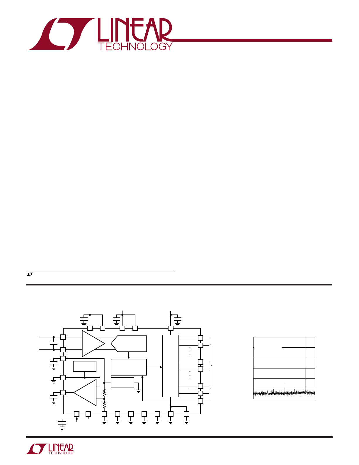
The LTC®1740 is a 6Msps, 14-bit sampling A/D converter
that draws only 245mW from either a single 5V or dual
±5V supplies. This easy-to-use device includes a high
dynamic range sample-and-hold and a programmable
precision reference.
The LTC1740 has a flexible input circuit that allows differential full-scale input ranges of ±2.5V and ±1.25V with the
internal reference, or any full-scale input range up to
±2.5V with an external reference. The input common
mode voltage is arbitrary, though a 2.5V reference is
provided for single supply applications.
DC specifications include 1LSB typical INL, 0.5LSB typical
DNL and no missing codes over temperature. Outstanding
AC performance includes 79dB S/(N␣ +␣ D) and 91dB SFDR
at an input frequency of 2.5MHz.
The unique differential input sample-and-hold can acquire
single-ended or differential input signals up to its 80MHz
bandwidth. The 75dB common mode rejection allows
users to eliminate ground loops and common mode noise
by measuring signals differentially from the source. A
separate output logic supply allows direct connection to
3V components.
BLOCK DIAGRA
5V
1µF
+
A
IN
1µF
1
2
3
4
5
–A
IN
V
CM
SENSE
V
REF
0V OR –5V
+
1000pF
V
IN
–
1µF
1µF
8
MODE SELECT
V
SS
30
29 6
W
5V 3V TO 5V
1µF
9
V
V
DD
DD
PIPELINED 14-BIT ADCS/H
DIGITAL CORRECTION
REFERENCE
2.250V
V
GND
SS
33
V
V
DD
DD
LOGIC
2.5V
GND7GND10GND34GND
31 11
BUFFERS
1932
OUTPUT
OV
OGND
1µF
DD
D13 (MSB)
D0 (LSB)
BUSY
CLK
OGND
28
4096-Point FFT
OF
36
12
D7
18
20
26
27
35
1740 TA01
DIGITAL
OUTPUT
6MHz CLK
D6
0
f
= 6MHz
SMPL
= 2.5MHz, 5V
f
IN
5V SUPPLY
–20
–40
–60
AMPLITUDE (dB)
–80
–100
–120
0
0.5
P-P
1.0 1.5 2.0
FREQUENCY (MHz)
2.5 3.0
1740 TA02
1740f
1
LTC1740
WW
W
U
ABSOLUTE MAXIMUM RATINGS
0VDD = VDD (Notes 1, 2)
Supply Voltage (VDD)................................................. 6V
Negative Supply Voltage (VSS) ................................ – 6V
Total Supply Voltage (VDD to VSS) ........................... 12V
Analog Input Voltage
(Note 3) .........................(VSS – 0.3V) to (VDD + 0.3V)
Digital Input Voltage
(Note 3) .........................(VSS – 0.3V) to (VDD + 0.3V)
Digital Output Voltage........(VSS – 0.3V) to (VDD + 0.3V)
Power Dissipation.............................................. 500mW
Operating Temperature Range
LTC1740C ............................................... 0°C to 70°C
LTC1740I............................................ –40°C to 85°C
Storage Temperature Range ................. –65°C to 150°C
Lead Temperature (Soldering, 10 sec).................. 300°C
W
PACKAGE/ORDER INFORMATION
+A
–A
V
SENSE
V
REF
GND
GND
V
V
GND
OGND
D13 (MSB)
D12
D11
D10
TOP VIEW
1
IN
2
IN
3
CM
4
5
6
7
8
DD
9
DD
10
11
12
13
14
15
16
D9
17
D8
18
D7
G PACKAGE
36-LEAD PLASTIC SSOP
T
= 125°C, θJA = 95°C/W
JMAX
OF
36
CLK
35
GND
34
V
33
DD
V
32
DD
GND
31
V
30
SS
V
29
SS
OGND
28
BUSY
27
D0
26
D1
25
D2
24
D3
23
D4
22
D5
21
D6
20
OV
19
DD
ORDER PART
NUMBER
LTC1740CG
LTC1740IG
UU
Consult LTC Marketing for parts specified with wider operating temperature
ranges.
U
CO VERTER CHARACTERISTICS
temperature range, otherwise specifications are at TA = 25°C. With internal 4.500V reference. Specifications are guaranteed for both
dual supply and single supply operation. (Notes 4, 5)
PARAMETER CONDITIONS MIN TYP MAX UNITS
Resolution (No Missing Codes) ● 14 Bits
Integral Linearity Error (Note 6) 1 ±2.5 LSB
Differential Linearity Error ● –1 0.5 1.25 LSB
Offset Error (Note 7) ±15 ±60 LSB
Full-Scale Error ±30 ±75 LSB
Full-Scale Tempco I
The ● denotes specifications which apply over the full operating
● ±80 LSB
= 0 ±15 ppm/°C
OUT(REF)
2
1740f
LTC1740
UU
A ALOG I PUT
specifications are at TA = 25°C. Specifications are guaranteed for both dual supply and single supply operation. (Note 4)
SYMBOL PARAMETER CONDITIONS MIN TYP MAX UNITS
V
IN
I
IN
C
IN
t
ACQ
t
AP
t
jitter
CMRR Analog Input Common Mode Rejection Ratio VSS < (–AIN = +AIN) < V
Analog Input Range V
Analog Input Leakage Current ● ±10 µA
Analog Input Capacitance Between Conversions 12 pF
Sample-and-Hold Acquisition Time 67 ns
Sample-and-Hold Aperture Delay Time –900 ps
Sample-and-Hold Aperture Delay Time Jitter 0.6 ps
The ● denotes specifications which apply over the full operating temperature range, otherwise
= 4.5V (SENSE = 0V) ● ±2.50 V
REF
V
= 2.25V (SENSE Tied to V
REF
External V
During Conversions 4 pF
(SENSE = 5V) ● ±V
REF
DD
) ● ±1.25 V
REF
/1.8 V
REF
75 dB
RMS
UW
DY A IC ACCURACY
SYMBOL PARAMETER CONDITIONS MIN TYP MAX UNITS
S/(N + D) Signal-to-Noise Plus Distortion Ratio 1MHz Input Signal 79.1 dB
THD Total Harmonic Distortion 1MHz Input Signal, First 5 Harmonics –90 dB
SFDR Spurious Free Dynamic Range 1MHz Input Signal 92 dB
Full-Power Bandwidth 80 MHz
Input Referred Noise 0.45 LSB
VDD = OVDD = 5V, VSS = 0V, V
2.5MHz Input Signal 79.0 dB
2.5MHz Input Signal, First 5 Harmonics –89 dB
2.5MHz Input Signal 91 dB
= 4.5V, AIN = –0.1dBFS, AC coupled differential input.
REF
RMS
UU U
I TER AL REFERE CE CHARACTERISTICS
TA = 25°C. Specifications are guaranteed for both dual supply and single supply operation. (Note 4)
PARAMETER CONDITIONS MIN TYP MAX UNITS
VCM Output Voltage I
VCM Output Tempco I
VCM Line Regulation 4.75V ≤ VDD ≤ 5.25V 0.6 mV/V
VCM Output Resistance 0.1mA ≤ I
V
Output Voltage SENSE = GND, I
REF
V
Output Tempco ±15 ppm/°C
REF
= 0 2.475 2.500 2.525 V
OUT
= 0 ±15 ppm/°C
OUT
–5.25V ≤ V
SENSE = V
SENSE = V
≤ –4.75V 0.03 mV/V
SS
≤ 0.1mA 8 Ω
OUT
= 0 4.500 V
OUT
, I
= 0 2.250 V
REF
OUT
DD
Drive V
External Reference
with V
REF
1740f
3
LTC1740
UU
DIGITAL I PUTS A D DIGITAL OUTPUTS
operating temperature range, otherwise specifications are at TA = 25°C. Specifications are guaranteed for both dual supply and single
supply operation. (Note 4)
SYMBOL PARAMETER CONDITIONS MIN TYP MAX UNITS
V
IH
V
IL
I
IN
C
IN
V
OH
V
OL
I
SOURCE
I
SINK
High Level Input Voltage V
Low Level Input Voltage VDD = 4.75V, VSS = 0V ● 0.8 V
Digital Input Current VIN = 0V to V
Digital Input Capacitance 1.8 pF
High Level Output Voltage 0VDD = 4.75V, IO = –10µA 4.74 V
Low Level Output Voltage 0VDD = 4.75V, IO = 160µA 0.05 V
Output Source Current V
Output Sink Current V
= 5.25V, VSS = 0V ● 2.4 V
DD
= 5.25V, VSS = –5V ● 2.4 V
V
DD
= 4.75V, VSS = –5V ● 0.8 V
V
DD
DD
= 4.75V, IO = –200µA ● 4.0 4.71 V
0V
DD
0V
= 2.7V, IO = –10µA 2.6 V
DD
= 2.7V, IO = –200µA ● 2.3 V
0V
DD
= 4.75V, IO = 1.6mA ● 0.10 0.4 V
0V
DD
= 2.7V, IO = 160µA 0.05 V
0V
DD
0V
= 2.7V, IO = 1.6mA ● 0.10 0.4 V
DD
= 0V, 0VDD = 5V 50 mA
OUT
= VDD, 0VDD = 5V 35 mA
OUT
The ● denotes specifications which apply over the full
● ±10 µA
WU
POWER REQUIRE E TS
otherwise specifications are at TA = 25°C. Specifications are guaranteed for both dual supply and single supply operation. (Note 4)
SYMBOL PARAMETER CONDITIONS MIN TYP MAX UNITS
V
OV
V
I
I
P
DD
DD
SS
DD
SS
D
Positive Supply Voltage (Note 9) 4.75 5.25 V
Output Supply Voltage (Note 9) 2.7 V
Negative Supply Voltage Dual Supply Mode –5.25 –4.75 V
Positive Supply Current ● 47 60 mA
Negative Supply Current ● 2.3 2.6 mA
Power Dissipation ● 245 300 mW
The ● denotes specifications which apply over the full operating temperature range,
DD
Single Supply Mode 0 V
UW
TI I G CHARACTERISTICS
range, otherwise specifications are at TA = 25°C. Specifications are guaranteed for both dual supply and single supply operation.
(Note 4)
SYMBOL PARAMETER CONDITIONS MIN TYP MAX UNITS
f
SAMPLE
t
CONV
t
ACQ
t
H
t
L
t
AP
t
1
t
2
Sampling Frequency ● 0.05 6 MHz
Conversion Time ● 100 135 ns
Acquisition Time (Note 9) ● 31 67 ns
CLK High Time (Note 9) ● 20 83.3 ns
CLK Low Time (Note 9) ● 20 83.3 ns
Aperature Delay of Sample-and-Hold –900 ps
CLK↑ to BUSY↓ 3.5 ns
BUSY↑ to Outputs Valid 1.5 ns
Data Latency 3 Cycles
The ● denotes specifications which apply over the full operating temperature
V
4
1740f
UW
TI I G CHARACTERISTICS
LTC1740
Note 1: Absolute Maximum Ratings are those values beyond which the life
of a device may be impaired.
Note 2: All voltage values are with respect to ground with GND and OGND
wired together (unless otherwise noted).
Note 3: When these pin voltages are taken below V
or above VDD, they
SS
will be clamped by internal diodes. This product can handle input currents
greater than 100mA below V
Note 4: VDD = 5V, VSS = –5V or 0V, f
or above VDD without latchup.
SS
= 6MHz, tr = tf = 5ns unless
SAMPLE
Note 6: Integral nonlinearity is defined as the deviation of a code from a
straight line passing through the actual endpoints of the transfer curve.
The deviation is measured from the center of the quantization band.
Note 7: Bipolar offset is the offset voltage measured from –0.5LSB
when the output code flickers between 00 0000 0000 0000 and
11 1111 1111 1111.
Note 8: Guaranteed by design, not subject to test.
Note 9: Recommended operating conditions.
otherwise specified.
Note 5: Linearity, offset and full-scale specifications apply for a
single-ended +A
input with –AIN tied to VCM for single supply and 0V for
IN
dual supply.
UW
TYPICAL PERFOR A CE CHARACTERISTICS
Typical INL at 6Msps Typical DNL at 6Msps
2.0
1.5
1.0
0.5
0
INL (LSB)
–0.5
–1.0
–1.5
–2.0
0
4096
8192
CODE
12288
16384
1740 G01
1.0
0.8
0.6
0.4
0.2
0
DNL (LSB)
–0.2
–0.4
–0.6
–0.8
–1.0
0
4096
8192
CODE
12288
16384
1740 G02
S/(N + D) vs Input Frequency
and Amplitude
80
VIN = 0dBFS
75
VIN = –6dBFS
70
65
S/(N + D) (dBc)
VIN = –20dBFS
60
DUAL SUPPLIES
5V INPUT RANGE
55
DIFFERENTIAL INPUT
6Msps
50
0.1
110
INPUT FREQUENCY (MHz)
100
1740 G03
S/(N + D) vs Input Frequency
and Amplitude
80
VIN = 0dBFS
75
VIN = –6dBFS
70
65
S/(N + D) (dBc)
VIN = –20dBFS
60
SINGLE SUPPLY
5V INPUT RANGE
55
DIFFERENTIAL INPUT
6Msps
50
0.1
110
INPUT FREQUENCY (MHz)
1740 G04
100
SFDR and THD
vs Input Frequency
95
90
85
80
75
70
AMPLITUDE (dB)
65
DUAL SUPPLIES
5V INPUT RANGE
60
= 0dBFS
A
IN
DIFFERENTIAL INPUT
55
6Msps
50
0.1
INPUT FREQUENCY (MHz)
SFDR
–THD
1 100
10
1740 G05
SFDR and THD
vs Input Frequency
95
90
85
80
75
70
AMPLITUDE (dB)
65
SINGLE SUPPLY
5V INPUT RANGE
60
= 0dBFS
A
IN
DIFFERENTIAL INPUT
55
6Msps
50
0.1
INPUT FREQUENCY (MHz)
SFDR
–THD
1 100
10
1740 G06
1740f
5

LTC1740
FREQUENCY (MHz)
0
0
–20
–40
–60
–80
–100
–120
–140
1.5 2.5
1740 G12
0.5 1
23
AMPLITIDE (dB)
SINGLE SUPPLY
6Msps
f
IN
= 2.5MHz, 5V
P-P
DIFFERENTIAL INPUT
UW
TYPICAL PERFOR A CE CHARACTERISTICS
Spurious-Free Dynamic Range
vs Input Amplitude
100
dBFS
90
80
70
dBc
60
SFDR (dBc AND dBFS)
50
0
–50
–40 –30 –20 –10
INPUT AMPLITUDE (dBFS)
DUAL SUPPLIES
5V INPUT RANGE
DIFFERENTIAL INPUT
6Msps
0
1740 G07
Spurious-Free Dynamic Range
vs Input Amplitude
100
90
80
70
60
SFDR (dBc AND dBFS)
50
0
–50
dBFS
dBc
SINGLE SUPPLY
5V INPUT RANGE
DIFFERENTIAL INPUT
6Msps
–40 –30 –20 –10
INPUT AMPLITUDE (dBFS)
S/(N + D) and SFDR
vs Sample Frequency Nonaveraged 4096 Point FFT
95
90
85
80
75
70
AMPLITUDE (dBc)
65
SINGLE SUPPLY
60
5V INPUT RANGE
DIFFERENTIAL INPUT
55
6Msps
50
1
SFDR
S/(N + D)
3
2
SAMPLE FREQUENCY (MHz)
56780
4
1740 G10
0
DUAL SUPPLIES
6Msps
–20
f
= 2.5MHz, 5V
IN
DIFFERENTIAL INPUT
–40
–60
–80
AMPLITIDE (dB)
–100
–120
–140
0
0.5 1
P-P
1.5 2.5
FREQUENCY (MHz)
AMPLITUDE (dBc)
0
1740 G08
23
1740 G11
S/(N + D) and SFDR
vs Sample Frequency
95
90
85
80
75
70
65
DUAL SUPPLIES
60
5V INPUT RANGE
DIFFERENTIAL INPUT
55
6Msps
50
1
SAMPLE FREQUENCY (MHz)
SFDR
S/(N + D)
3
2
56780
4
Nonaveraged 4096 Point FFT
1740 G09
6
(mA)
DD
I
IDD vs Clock Frequency ISS vs Clock Frequency
49
47
45
V
= 4.5V
43
41
39
37
35
0
REF
12
CLOCK FREQUENCY (MHz)
V
= 2.25V
REF
46
35
1740 G13
2.5
2.0
1.5
(mA)
SS
I
1.0
0.5
0
0
234
1
CLOCK FREQUENCY (MHz)
56
1740 G14
1740f

LTC1740
U
UU
PIN FUNCTIONS
+AIN (Pin 1):
–AIN (Pin 2): Negative Analog Input.
VCM (Pin 3): 2.5V Reference Output. Optional input com-
mon mode for single supply operation. Bypass to GND
with a 1µF to 10µF ceramic capacitor.
SENSE (Pin 4): Reference Programming Pin. Ground
selects V
Connect SENSE to VDD to drive V
reference. Connect SENSE directly to VDD, V
Do not drive SENSE with a logic signal.
V
(Pin 5): DAC Reference. Bypass to GND with a 1µF to
REF
10µF ceramic capacitor.
GND (Pins 6, 7, 10, 31, 34): Analog Power Ground.
VDD (Pins 8, 9): Analog 5V Supply. Bypass to GND with a
1µF to 10µF ceramic capacitor. (Do not share a capacitor
with Pins 32 and 33.)
OGND (Pins 11, 28): Output Logic Ground. Connect to
GND.
Positive Analog Input.
= 4.5V. Short to V
REF
for V
REF
REF
REF
with an external
REF
= 2.25V.
or GND.
OVDD (Pin 19): Positive Supply for the Output Logic. Can
be 2.7V to 5.25V. Bypass to GND with a 1µF to 10µF
ceramic capacitor.
BUSY (Pin 27): BUSY is low when a conversion is in
progress. When a conversion is finished and the ADC is
acquiring the input signal, BUSY is high. Either the falling
edge of BUSY or the rising edge of CLK can be used to
latch the output data.
VSS (Pins 29, 30): Negative Supply. Can be –5V or 0V. If
VSS is not shorted to GND, bypass to GND with a 1µF
ceramic capacitor.
VDD (Pins 32, 33): Analog 5V Supply. Bypass to GND with
a 1µF to 10µF ceramic capacitor (do not share a capacitor
with Pins 8, 9).
CLK (Pin 35): Conversion Start Signal. This active high
signal starts a conversion on its rising edge.
OF (Pin 36): Overflow Output. This signal is high when the
digital output is 01 1111 1111 1111 or 10 0000 0000 0000.
D13 to D0 (Pins 12 to 18, 20 to 26): Data Outputs. The
output format is two’s complement.
1740f
7
LTC1740
UU
W
FUNCTIONAL BLOCK DIAGRA
5V
V
DD
+
A
IN
–A
IN
V
CM
MODE SELECT
SENSE
V
REF
SS
0V OR –5V
GND
PIPELINED 14-BIT ADCS/H
DIGITAL CORRECTION
LOGIC
2.5V
REFERENCE
GNDV
3V TO 5V
OV
OUTPUT
BUFFERS
OGND
DD
OF
D13 (MSB)
D0 (LSB)
BUSY
CLK
1740 FBD
UWW
TI I G DIAGRA
ANALOG
INPUT
CLK
DATA
OUTPUT
BUSY
N
t
t
t
2
N + 1
N + 2
t
CLOCK
t
H
L
CONV
N-3 N-2 N-1 N
t
1
t
ACQ
N + 3
1740 TD
8
1740f

WUUU
APPLICATIO S I FOR ATIO
LTC1740
Conversion Details
The LTC1740 is a high performance 14-bit A/D converter
that operates up to 6Msps. It is a complete solution with
an on-chip sample-and-hold, a 14-bit pipelined CMOS
ADC and a low drift programmable reference. The digital
output is parallel, with a 14-bit two’s complement format
and an out-of-range (overflow) bit.
The rising edge of the CLK begins the conversion. The
differential analog inputs are simultaneously sampled and
passed on to the pipelined A/D. After two more conversion
starts (plus a 100ns conversion time) the digital outputs
are updated with the conversion result and will be ready for
capture on the third rising clock edge. Thus even though
a new conversion is begun every time CLK goes high, each
result takes three clock cycles to reach the output.
The analog signals that are passed from stage to stage in
the pipelined A/D are stored on capacitors. The signals on
these capacitors will be lost if the delay between conversions is too long. For accurate conversion results, the part
should be clocked faster than 50kHz.
In some pipelined A/D converters if there is no clock present,
dynamic logic on the chip will droop and the power consumption sharply increases. The LTC1740 doesn’t have
this problem. If the part is not clocked for 1ms, an internal
timer will refresh the dynamic logic. Thus the clock can be
turned off for long periods of time to save power.
Power Supplies
The LTC1740 will operate from either a single 5V or dual
±5V supply, making it easy to interface the analog input to
single or dual supply systems. The digital output drivers
have their own power supply pin (OVDD) which can be set
from 3V to 5V, allowing direct connection to either 3V or
5V digital systems. For single supply operation, VSS should
be connected to analog ground. For dual supply operation,
VSS should be connected to –5V. All VDD pins should be
connected to a clean 5V analog supply. (Don’t connect V
DD
to a noisy system digital supply.)
Analog Input Range
The LTC1740 has a flexible analog input with a wide
selection of input ranges. The input range is always
differential and is set by the voltage at the V
REF
pin
(Figure␣ 1). The input range of the A/D core is fixed at
±V
/1.8. The reference voltage, V
REF
, is either set by the
REF
on-chip voltage reference or directly driven by an external
voltage.
Internal Reference
Figure 2 shows a simplified schematic of the LTC1740
reference circuitry. An on-chip temperature compensated
bandgap reference (VCM) is factory trimmed to 2.500V.
The voltage at the V
to ±V
/1.8. An internal voltage divider converts VCM to
REF
pin sets the input span of the ADC
REF
2.250V, which is connected to a reference amplifier. The
reference programming pin, SENSE, controls how the
V
REF
SENSE
1µF
+
R1
5k
R2
5k
LOGIC
–
TO
ADC
1k
+A
IN
+
V
IN
–A
–
V
Figure 1. Analog Input Circuit
REF
±V
REF
1.8
IN
ADC
CORE
1740 F01
2.5V
REFERENCE
2.250V
V
CM
1µF
1740 F02
Figure 2. Reference Circuit
1740f
9

LTC1740
WUUU
APPLICATIO S I FOR ATIO
reference amplifier drives the V
pin. If SENSE is tied to
REF
ground, the reference amplifier feedback is connected to
the R1/R2 voltage divider, thus making V
SENSE is tied to V
connected to SENSE thus making V
, the reference amplifier feedback is
REF
REF
= 4.500V. If
REF
= 2.250V. If SENSE
is tied to VDD, the reference amplifier is disconnected from
V
and V
REF
additional resistors between V
and GND, V
can be driven by an external voltage. With
REF
and SENSE, and SENSE
REF
can be set to any voltage between 2.250V
REF
and 4.5V.
An external reference or a DAC can be used to drive V
REF
over a 0V to 5V range (Figures 3a and 3b). The input
impedance of the V
required for high accuracy. Driving V
pin is 1kΩ, so a buffer may be
REF
with a DAC is
REF
useful in applications where the peak input signal amplitude may vary. The input span of the ADC can then be
adjusted to match the peak input signal, maximizing the
signal-to-noise ratio.
5V
V
IN
V
LT1019A-2.5
OUT
1µF
V
REF
SENSE5V
LTC1740
Both the VCM and V
pins must be bypassed with
REF
capacitors to ground. For best performance, 1µF or larger
ceramic capacitors are recommended. For the case of
external circuitry driving V
used at V
so the input range can be changed quickly.
REF
, a smaller capacitor can be
REF
In this case, a 0.2µF or larger ceramic capacitor is
acceptable.
The VCM pin is a low output impedance 2.5V reference that
can be used by external circuitry. For single 5V supply
applications it is convenient to connect A
–
directly to the
IN
VCM pin.
Driving the Analog Inputs
The differential inputs of the LTC1740 are easy to drive.
The inputs may be driven differentially or single-ended
(i.␣ e., the A
+
A
inputs are simultaneously sampled and any common
IN
–
input is held at a fixed value). The A
IN
IN
–
and
mode signal is reduced by the high common mode rejection of the sample-and-hold circuit. Any common mode
input value is acceptable as long as the input pins stay
between VDD and VSS. During conversion the analog
inputs are high impedance. At the end of conversion the
inputs draw a small current spike while charging the
sample-and-hold.
V
CM
1µF
Figure 3a. Using the LT1019-2.5 as an
External Reference; Input Range = ±1.39V
LTC1740
V
REF
1µF
5k
SENSE
LTC1450
Figure 3b. Driving V
5k
1µF
V
CM
with a DAC
REF
1740 F03a
For superior dynamic performance in dual supply mode,
the LTC1740 should be operated with the analog inputs
centered at ground, and in single supply mode the inputs
should be centered at 2.5V. For the best dynamic performance, the analog inputs can be driven differentially via a
transformer or differential amplifier.
DC Coupling the Input
2.250V
+
–
In many applications the analog input signal can be
directly coupled to the LTC1740 inputs. If the input signal
is centered around ground, such as when dual supply op
amps are used, simply connect A
–
to ground and con-
IN
nect VSS to –5V (Figure 4). In a single power supply
1740 F03b
system with the input signal centered around 2.5V, connect A
–
to VCM and VSS to ground (Figure 5). If the input
IN
signal is not centered around ground or 2.5V, the voltage
for A
–
must be generated externally by a resistor divider
IN
or a voltage reference (Figure 6).
1740f
10

WUUU
APPLICATIO S I FOR ATIO
LTC1740
5V
0V
V
IN
1µF
+A
–A
V
CM
IN
LTC1740
IN
V
SS
–5V
1405 F04
Figure 4. DC Coupling a Ground Centered Signal
(Dual Supply System)
5V
2.5V
V
IN
1µF
+A
–A
V
CM
IN
LTC1740
IN
V
SS
1740 F05
Figure 5. DC Coupling a Signal Centered Around
2.5V (Single Supply System)
5V
2.500V
V
0V
5V
IN
1.25V
1µF
+A
IN
LTC1740
–A
IN
V
REF
SENSE
V
SS
1740 F06
+A
–A
V
CM
5V
IN
LTC1740
IN
V
SS
1740 F07
C
0V
V
IN
RR
C
1µF
Figure 7. AC Coupling to the LTC1740. Note That the Input Signal
Can Almost Always Be Directly Coupled with Better Performance
+A
–A
V
CM
5V
IN
LTC1740
IN
V
SS
1740 F08a
V
IN
MINI CIRCUITS
T1-1T
15Ω
1000pF
15Ω
1µF
Figure 8a. Single Supply Transformer Coupled Input
+A
–A
V
CM
5V
IN
LTC1740
IN
V
SS
–5V
1740 F08b
V
IN
MINI CIRCUITS
T1-1T
15Ω
1000pF
15Ω
1µF
Figure 6. DC Coupling a 0V to 2.5V Signal
AC Coupling the Input
The analog inputs to the LTC1740 can also be AC coupled
through a capacitor, though in most cases it is simpler to
directly couple the input to the ADC. Figure 7 shows an
example where the input signal is centered around ground
and the ADC operates from a single 5V supply. Note that
the performance would improve if the ADC was operated
from a dual supply and the input was directly coupled (as
in Figure 4). With AC coupling the DC resistance to ground
should be roughly matched for A
IN
+
and A
–
to maintain
IN
offset accuracy.
Figure 8b. Dual Supply Transformer Coupled Input
Differential Operation
The THD and SFDR performance of the LTC1740 can be
improved by using a center tap RF transformer to drive the
inputs differentially. Though the signal can no longer be
DC coupled, the improvement in dynamic performance
makes this an attractive solution for some applications.
Typical connections for single and dual supply systems
are shown in Figures 8a and 8b. Good choices for transformers are the Mini Circuits T1-1T (1:1 turns ratio) and
T4-6T (1:4 turns ratio). For best results the transformer
should be located close to the LTC1740 on the printed
circuit board.
1740f
11

LTC1740
+A
IN
V
IN
LTC1740
1740 F09
–A
IN
1000pF
30Ω
WUUU
APPLICATIO S I FOR ATIO
Choosing an Input Amplifier
Choosing an input amplifier is easy if a few requirements
are taken into consideration. First, to limit the magnitude
of the voltage spike seen by the amplifier from charging
the sampling capacitor, choose an amplifier that has a low
output impedance (<100Ω) at the closed-loop bandwidth
frequency. For example, if an amplifier is used in a gain
of␣ 1 and has a unity-gain bandwidth of 50MHz, then the
output impedance at 50MHz must be less than 100Ω. The
second requirement is that the closed-loop bandwidth
must be greater than 50MHz to ensure adequate smallsignal settling for full throughput rate. If slower op amps
are used, more settling time can be provided by increasing
the time between conversions.
The best choice for an op amp to drive the LTC1740 will
depend on the application. Generally applications fall into
two categories: AC applications where dynamic specifications are most critical and time domain applications where
DC accuracy and settling time are most critical.
Input Filtering
The noise and the distortion of the input amplifier and
other circuitry must be considered since they will add to
the LTC1740 noise and distortion. The small-signal bandwidth of the sample-and-hold circuit is 80MHz. Any noise
or distortion products that are present at the analog inputs
will be summed over this entire bandwidth. Noisy input
circuitry should be filtered prior to the analog inputs to
minimize noise. A simple 1-pole RC filter is sufficient for
many applications.
Figure 9. RC Input Filter
used since these components can add distortion. NPO and
silver mica type dielectric capacitors have excellent linearity. Carbon surface mount resistors can generate distortion from self-heating and from damage that may occur
during soldering. Metal film surface mount resistors are
much less susceptible to both problems.
Digital Outputs and Overflow Bit (OF)
Figure 10 shows the ideal input/output characteristics for
the LTC1740. The output data is two’s complement binary
for all input ranges and for both single and dual supply
operation. One LSB = V
/(0.9 • 16384). To create a
REF
straight binary output, invert the MSB (D13). The overflow
bit (OF) indicates when the analog input is outside the
input range of the converter. OF is high when the output
code is 10 0000 0000 0000 or 01 1111 1111 1111.
1
OVERFLOW
BIT
0
011…111
011…110
011…101
For example, Figure 9 shows a 1000pF capacitor from
+AIN to –AIN and a 30Ω source resistor to limit the input
OUTPUT CODE
bandwidth to 5.3MHz. The 1000pF capacitor also acts as
a charge reservoir for the input sample-and-hold and isolates the amplifier driving VIN from the ADC’s small current
glitch. In undersampling applications, an input capacitor
this large may prohibitively limit the input bandwidth.
100…010
100…001
100…000
–(FS – 1LSB) FS – 1LSB
INPUT VOLTAGE (V)
1740 F10
If this is the case, use as large an input capacitance as
possible. High quality capacitors and resistors should be
12
Figure 10. LTC1740 Transfer Characteristics
1740f

WUUU
APPLICATIO S I FOR ATIO
LTC1740
Full-Scale and Offset Adjustment
In applications where absolute accuracy is important,
offset and full-scale errors can be adjusted to zero. Offset
error should be adjusted before full-scale error. Figure 11
shows a method for error adjustment for a dual supply,
5.00V input range application. For zero offset error apply
–0.15mV (i.␣ e., – 0.5LSB) at +AIN and adjust R1 until the
output code flickers between 00 0000 0000 0000 and 11
1111 1111 1111. For full-scale adjustment, apply an input
voltage of
2.49954V (FS – 1.5LSBs) at + AIN and adjust R2
until the output code flickers between 01 1111 1111 1110
and 01 1111 1111 1111.
Digital Output Drivers
The LTC1740 output drivers can interface to logic operating from 3V to 5V by setting OVDD to the logic power
supply. OVDD requires a 1µF decoupling capacitor. To
prevent digital noise from affecting performance, the load
capacitance on the digital outputs should be minimized. If
large capacitive loads are required, (>30pF) external buffers or 100Ω resistors in series with the digital outputs are
suggested.
Timing
The conversion start is controlled by the rising edge of the
CLK pin. Once a conversion is started it cannot be stopped
or restarted until the conversion cycle is complete. Output
data is updated at the end of conversion, or about 100ns
after a conversion is begun. There is an additional two
cycle pipeline delay, so the data for a given conversion is
output two full clock cycles plus 100ns after the convert
start. Thus output data can be latched on the third CLK
rising edge after the rising edge that samples the input.
Clock Input
The LTC1740 only uses the rising edge of the CLK pin for
internal timing, and CLK doesn’t necessarily need to have
a 50% duty cycle. For optimal AC performance the rise
time of the CLK should be less than 5ns. If the available
clock has a rise time slower than 5ns, it can be locally sped
up with a logic gate. The clock can be driven with 5V
CMOS, 3V CMOS or TTL logic levels.
5V
+A
V
10k1µF
10k
R2
1k
IN
24k
100Ω
5V
R1
50k
–5V
Figure 11. Offset and Full-Scale Adjust Circuit
IN
–A
IN
LTC1740
V
REF
SENSE
V
–5V
SS
1740 F11
1740f
13

LTC1740
WUUU
APPLICATIO S I FOR ATIO
As with all fast ADCs, the noise performance of the
LTC1740 is sensitive to clock jitter when high speed inputs
are present. The SNR performance of an ADC when the
performance is limited by jitter is given by:
SNR = –20log (2πfINtJ)dB
where fIN is the frequency of an input sine wave and tJ is
the root-mean-square jitter due to the clock, the analog
input and the A/D aperture jitter. To minimize clock jitter,
use a clean clock source such as a crystal oscillator, treat
the clock signals as sensitive analog traces and use
dedicated packages with good supply bypassing for any
clock drivers.
Board Layout
To obtain the best performance from the LTC1740, a
printed circuit board with a ground plane is required.
Layout for the printed circuit board should ensure that
digital and analog signal lines are separated as much as
possible. In particular, care should be taken not to run any
digital track alongside an analog signal track.
should be connected to the analog ground plane at only
one point, near the OGND pin (Pin 28).
The analog ground plane should be as close to the ADC as
possible. Care should be taken to avoid making holes in the
analog ground plane under and around the part. To accomplish this, we recommend placing vias for power and
signal traces outside the area containing the part and the
decoupling capacitors (Figure 13).
Supply Bypassing
High quality, low series resistance ceramic 1µF capacitors
should be used at the VDD pins, VCM and V
. If VSS is
REF
connected to –5V it should also be bypassed to ground
with 1µF. In single supply operation VSS should be shorted
to the ground plane as close to the part as possible. OV
DD
requires a 1µF decoupling capacitor to ground. Surface
mount capacitors such as the AVX 0805ZC105KAT provide excellent bypassing in a small board space. The traces
connecting the pins and the bypass capacitors must be
kept short and should be made as wide as possible.
An analog ground plane separate from the logic system
ground should be placed under and around the ADC.
Pins␣ 6, 7, 10, 31, 34 (GND), Pins 11, 28 (OGND) and all
other analog grounds should be connected to this ground
plane. In single supply mode, Pins 29, 30 (VSS) should
also be connected to this ground plane. All bypass capacitors for the LTC1740 should also be connected to this
ground plane (Figure 12). The digital system ground
1
+A
IN
CM
V
REF
3
5
1µF
GND
GND
7
6
1µF
ANALOG GROUND PLANE
V
V
DD
DD
8
9
1µF
V
–A
IN
2
ANALOG
INPUT
CIRCUITRY
+
–
1000pF
LTC1740
PLACE NON-GROUND
VIAS AWAY FROM
GROUND PLANE AND
BYPASS CAPACITORS
AVOID BREAKING GROUND PLANE
IN THIS AREA
Figure 13. Cross Section of the LTC1740 Printed Circuit Board
LTC1740
GND
10
OGND
V
OV
DD
19
11
1µF
GND
V
V
SS
SS
1µF
31
30
29
GNDV
DD
DD
32
1µF
OGND
33
28
34
1740 F12
DIGITAL
SYSTEM
BYPASS
CAPACITOR
ANALOG
GROUND
PLANE
1740 F13
14
Figure 12. Power Supply Grounding
1740f

PACKAGE DESCRIPTION
U
G Package
36-Lead Plastic SSOP (5.3mm)
(Reference LTC DWG # 05-08-1640)
1.25 ±0.12
12.50 – 13.10*
(.492 – .516)
LTC1740
2526 22 21 20 19232427282930313233343536
7.8 – 8.2
0.42 ±0.03 0.65 BSC
RECOMMENDED SOLDER PAD LAYOUT
5.00 – 5.60**
(.197 – .221)
0.09 – 0.25
(.0035 – .010)
NOTE:
1. CONTROLLING DIMENSION: MILLIMETERS
2. DIMENSIONS ARE IN
3. DRAWING NOT TO SCALE
*
DIMENSIONS DO NOT INCLUDE MOLD FLASH. MOLD FLASH
SHALL NOT EXCEED .152mm (.006") PER SIDE
**
DIMENSIONS DO NOT INCLUDE INTERLEAD FLASH. INTERLEAD
FLASH SHALL NOT EXCEED .254mm (.010") PER SIDE
0.55 – 0.95
(.022 – .037)
MILLIMETERS
(INCHES)
° – 8°
0
5.3 – 5.7
12345678 9 10 11 12 14 15 16 17 1813
0.65
(.0256)
BSC
0.22 – 0.38
(.009 – .015)
7.40 – 8.20
(.291 – .323)
2.0
(.079)
0.05
(.002)
G36 SSOP 0802
Information furnished by Linear Technology Corporation is believed to be accurate and reliable.
However, no responsibility is assumed for its use. Linear Technology Corporation makes no representation that the interconnection of its circuits as described herein will not infringe on existing patent rights.
1740f
15

LTC1740
RELATED PARTS
PART NUMBER DESCRIPTION COMMENTS
LTC1405 12-Bit, 5Msps Sampling ADC with Parallel Output Pin Compatible with the LTC1420
LTC1406 8-Bit, 20Msps ADC Undersampling Capability up to 70MHz
LTC1411 14-Bit, 2.5Msps ADC 5V, No Pipeline Delay, 80dB SINAD
LTC1412 12-Bit, 3Msps, Sampling ADC ±5V, No Pipeline Delay, 72dB SINAD
LTC1414 14-Bit, 2.2Msps ADC ±5V, 81dB SINAD and 95dB SFDR
LTC1420 12-Bit, 10Msps ADC 71dB SINAD and 83dB SFDR at Nyquist
LT1461 Micropower Precision Series Reference 0.04% Max Initial Accuracy, 3ppm/°C Drift
LTC1666 12-Bit, 50Msps DAC Pin Compatible with the LTC1668, LTC1667
LTC1667 14-Bit, 50Msps DAC Pin Compatible with the LTC1668, LTC1666
LTC1668 16-Bit, 50Msps DAC 16-Bit, No Missing Codes, 90dB SINAD, –100dB THD
LTC1741 12-Bit, 65Msps ADC Pin Compatible with the LTC1748
LTC1742 14-Bit, 65Msps ADC Pin Compatible with the LTC1748
LTC1743 12-Bit, 50Msps ADC Pin Compatible with the LTC1748
LTC1744 14-Bit, 50Msps ADC Pin Compatible with the LTC1748
LTC1745 12-Bit, 25Msps ADC Pin Compatible with the LTC1748
LTC1746 14-Bit, 25Msps ADC Pin Compatible with the LTC1748
LTC1747 12-Bit, 80Msps ADC Pin Compatible with the LTC1748
LTC1748 14-Bit, 80Msps ADC 76.3dB SNR and 90dB SFDR
LT1807 325MHz, Low Distortion Dual Op Amp Rail-to-Rail Input and Output
16
Linear Technology Corporation
1630 McCarthy Blvd., Milpitas, CA 95035-7417
(408) 432-1900 ● FAX: (408) 434-0507
●
www.linear.com
1740f
LT/TP 0603 1K • PRINTED IN USA
LINEAR TECHNOLOGY CORPORATION 2003
 Loading...