

Linear Technology LTC1606 Datasheet
FEATURES
Final Electrical Specifications
■
Sample Rate: 250ksps
■
Single 5V Supply
■
Bipolar Input Range: ±10V
■
Signal-to-Noise Ratio: 90dB Typ
■
Power Dissipation: 75mW Typ
■
Integral Nonlinearity: ±2.0LSB Max
■
Guaranteed No Missing Codes
■
Operates with Internal or External Reference
■
Internal Synchronized Clock
■
28-Pin SSOP Package
■
Improved 2nd Source to AD976A and ADS7805
U
APPLICATIONS
■
Industrial Process Control
■
Multiplexed Data Acquisition Systems
■
High Speed Data Acquisition for PCs
■
Digital Signal Processing
LTC1606
16-Bit, 250ksps,
Single Supply ADC
March 2000
U
DESCRIPTION
The LTC®1606 is a 250ksps, sampling 16-bit A/D converter that draws only 75mW (typical) from a single 5V
supply. This easy-to-use device includes sample-andhold, precision reference, switched capacitor successive
approximation A/D and trimmed internal clock.
The LTC1606’s input range is an industry standard ±10V.
Maximum DC specs include ±2.0LSB INL and 16 bits no
missing codes over temperature. An external reference
can be used if greater accuracy over temperature is
needed.
The 90dB signal-to-noise ratio offers an improvement of
3dB over competing devices, and the RMS transition noise
is reduced (0.65LSB vs 1LSB) relative to competitive
parts.
The ADC has a microprocessor compatible, 16-bit or two
byte parallel output port. A convert start input and a data
ready signal (BUSY) ease connections to FIFOs, DSPs and
microprocessors.
, LTC and LT are registered trademarks of Linear Technology Corporation.
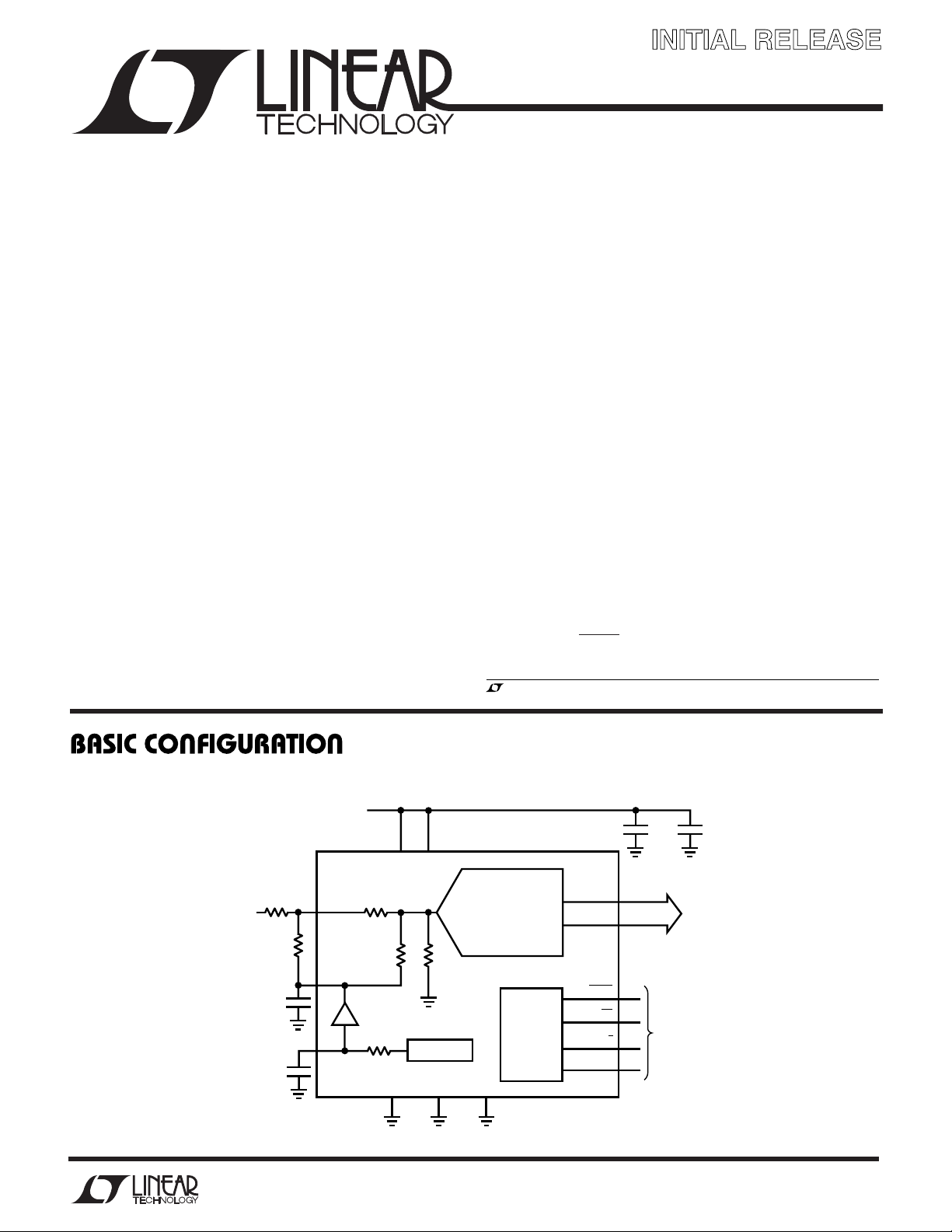
±10V
INPUT
Low Power, 250kHz, 16-Bit Sampling ADC on 5V Supply
5V
6 TO 13
15 TO 22
26
25
24
23
10µF
DIGITAL
CONTROL
SIGNALS
28 27
V
DIGVANA
200Ω
1
33.2k
4
4.096V
10µF
3
2.5V
2.2µF
Information furnished by Linear Technology Corporation is believed to be accurate and reliable.
However, no responsibility is assumed for its use. Linear Technology Corporation makes no representation that the interconnection of its circuits as described herein will not infringe on existing patent rights.
V
CAP
REF
7.35k
IN
2.5k 9k
1.64x
BUFFER
4k
REFERENCE
AGND1
AGND25DGND
2
16-BIT
SAMPLING ADC
CONTROL
LOGIC AND
TIMING
14
D15 TO D0
BUSY
CS
R/C
BYTE
1606 TA01
0.1µF
16-BIT
OR 2 BYTE
PARALLEL
BUS
1
LTC1606
W
O
A
(Notes 1, 2)
V
ANA
V
DIG
V
DIG
LUTEXI TIS
S
.......................................................................... 7V
to V
........................................................... 0.3V
ANA
........................................................................... 7V
A
WUW
U
ARB
G
Ground Voltage Difference
DGND, AGND1 and AGND2 .............................. ±0.3V
Analog Inputs (Note 3)
VIN..................................................................... ±25V
CAP ............................ V
+ 0.3V to AGND2 – 0.3V
ANA
REF....................................Indefinite Short to AGND2
Momentary Short to V
Digital Input Voltage (Note 4) ........ V
Digital Output Voltage........ V
– 0.3V to V
DGND
– 0.3V to 10V
DGND
DIG
ANA
+ 0.3V
Power Dissipation.............................................. 500mW
Operating Ambient Temperature Range
LTC1606AC/LTC1606C............................0°C to 70°C
LTC1606AI/LTC1606I ......................... – 40°C to 85°C
Storage Temperature Range ................. –65°C to 150°C
Lead Temperature (Soldering, 10 sec).................. 300°C
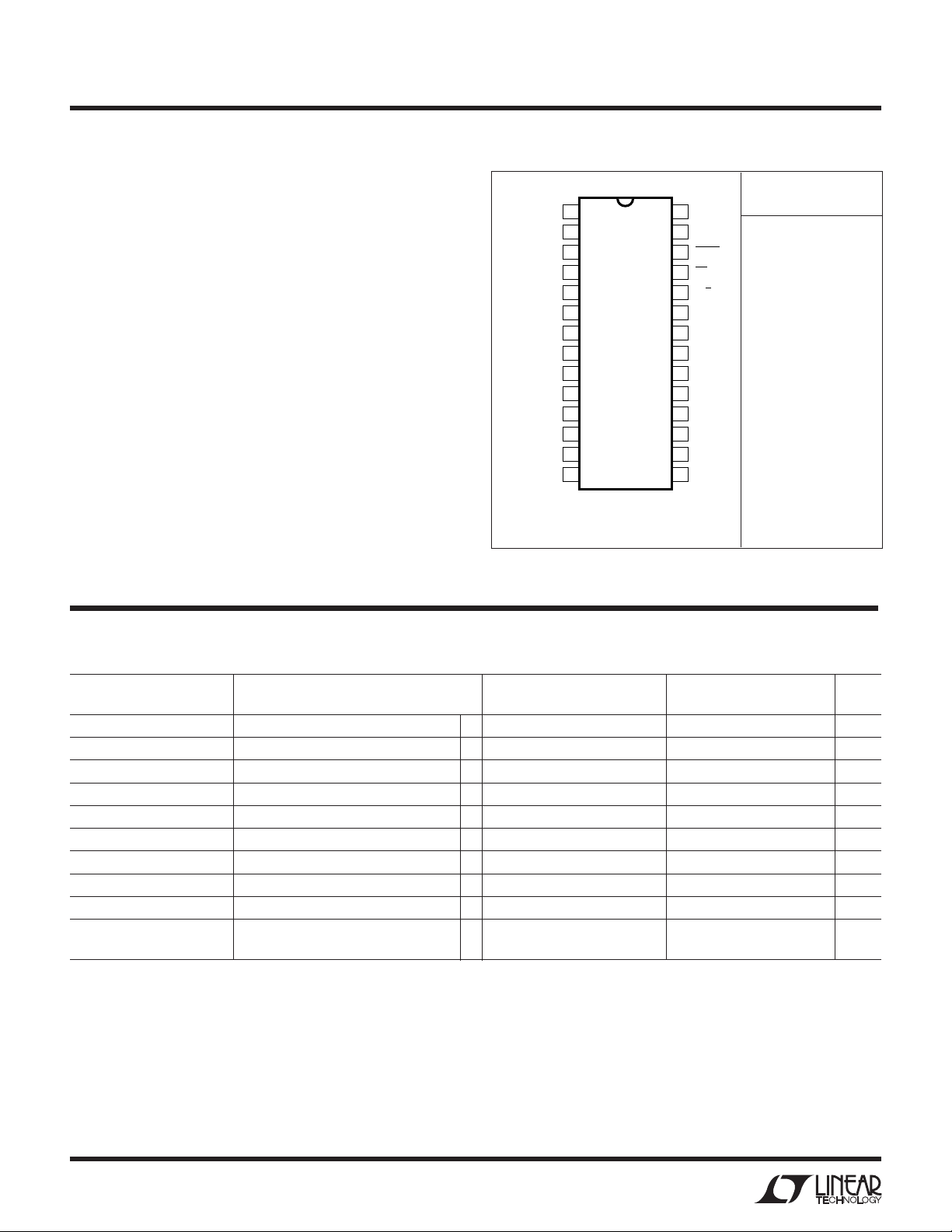
/
PACKAGE
V
IN
AGND1
REF
CAP
AGND2
D15 (MSB)
D14
D13
D12
D11
D10
D9
D8
DGND
Consult factory for Military grade parts.
O
RDER I FOR ATIO
TOP VIEW
1
2
3
4
5
6
7
8
9
10
11
12
13
14
G PACKAGE
28-LEAD PLASTIC SSOP
T
= 125°C, θJA = 95°C/W
JMAX
28
27
26
25
24
23
22
21
20
19
18
17
16
15
V
DIG
V
ANA
BUSY
CS
R/C
BYTE
D0
D1
D2
D3
D4
D5
D6
D7
WU
ORDER PART
NUMBER
LTC1606ACG
LTC1606AIG
LTC1606CG
LTC1606IG
U
U
CONVERTER CHARACTERISTICS
temperature range, otherwise specifications are at TA = 25°C. (Notes 5, 6)
PARAMETER CONDITIONS MIN TYP MAX MIN TYP MAX UNITS
Resolution ● 16 16 Bits
No Missing Codes ● 15 16 Bits
Transition Noise 0.65 0.65 LSB
Integral Linearity Error (Note 7) ● ±3 ±2 LSB
Bipolar Zero Error Ext. Reference = 2.5V (Note 8) ● ±10 ±10 mV
Bipolar Zero Error Drift ±2 ±2 ppm/°C
Full-Scale Error Drift ±7 ±5 ppm/°C
Full-Scale Error Ext. Reference = 2.5V (Notes 12, 13) ● ±0.50 ±0.25 %
Full-Scale Error Drift Ext. Reference = 2.5V ±2 ±2 ppm/°C
Power Supply Sensitivity
= V
DIG
= V
DD
V
ANA
VDD = 5V ±5% (Note 9) ±8 ±8 LSB
The ● indicates specifications which apply over the full operating
LTC1606 LTC1606A
RMS
2
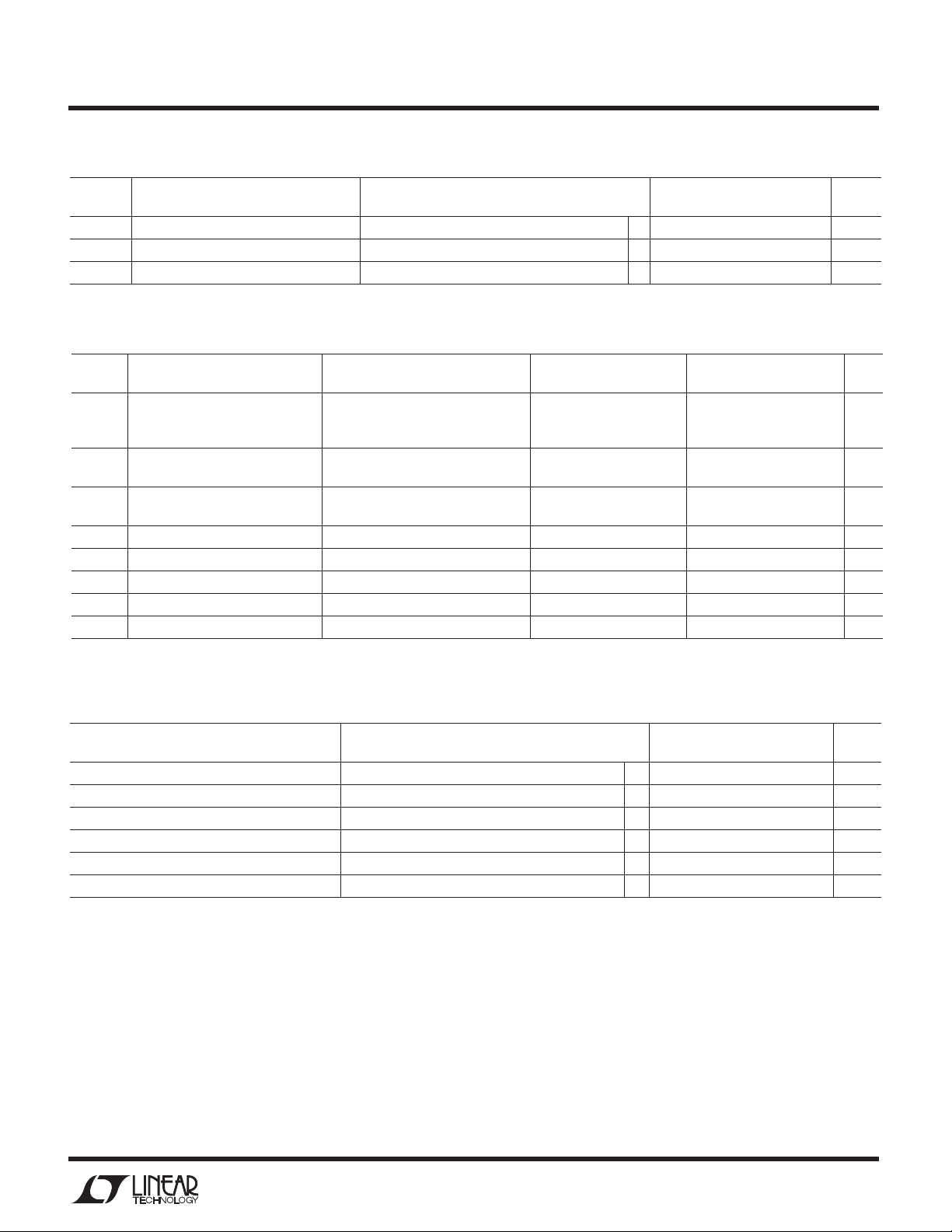
LTC1606
UU
ANALOG INPUT
specifications are at TA = 25°C. (Note 5)
SYMBOL PARAMETER CONDITIONS MIN TYP MAX UNITS
V
IN
C
IN
R
IN
Analog Input Range (Note 9) 4.75V ≤ V
Analog Input Capacitance 10 pF
Analog Input Impedance 10 kΩ
The ● indicates specifications which apply over the full operating temperature range, otherwise
LTC1606/LTC1606A
≤ 5.25V, 4.75V ≤ V
ANA
≤ 5.25V ● ±10 V
DIG
UW
DYNAMIC ACCURACY
SYMBOL PARAMETER CONDITIONS MIN TYP MAX MIN TYP MAX UNITS
S/(N + D) Signal-to-(Noise + Distortion) Ratio 1kHz Input Signal (Note 14) 90 90 dB
THD Total Harmonic Distortion 1kHz Input Signal, First 5 Harmonics –102 – 102 dB
Peak Harmonic or Spurious Noise 1kHz Input Signal –102 –102 dB
Full-Power Bandwidth (Note 15) 275 275 kHz
Aperture Delay 40 40 ns
Aperture Jitter Sufficient to Meet AC Specs Sufficient to Meet AC Specs
Transient Response Full-Scale Step (Note 9) 2 2 µs
Overvoltage Recovery (Note 16) 150 150 ns
(Notes 5, 14)
LTC1606 LTC1606A
10kHz Input Signal 90 87 90 dB
20kHz, –60dB Input Signal 30 30 dB
10kHz Input Signal, First 5 Harmonics –94 –89 – 94 dB
10kHz Input Signal –94 –94 dB
UU U
INTERNAL REFERENCE CHARACTERISTICS
operating temperature range, otherwise specifications are at TA = 25°C. (Note 5)
PARAMETER CONDITIONS MIN TYP MAX UNITS
V
Output Voltage I
REF
V
Output Tempco I
REF
Internal Reference Source Current 1 µA
External Reference Voltage for Specified Linearity (Notes 9, 10) 2.30 2.50 2.70 V
External Reference Current Drain Ext. Reference = 2.5V (Note 9) ● 100 µA
CAP Output Voltage I
= 0 ● 2.470 2.500 2.520 V
OUT
= 0 ±5 ppm/°C
OUT
= 0 4.096 V
OUT
The ● indicates specifications which apply over the full
LTC1606/LTC1606A
3
LTC1606
UU
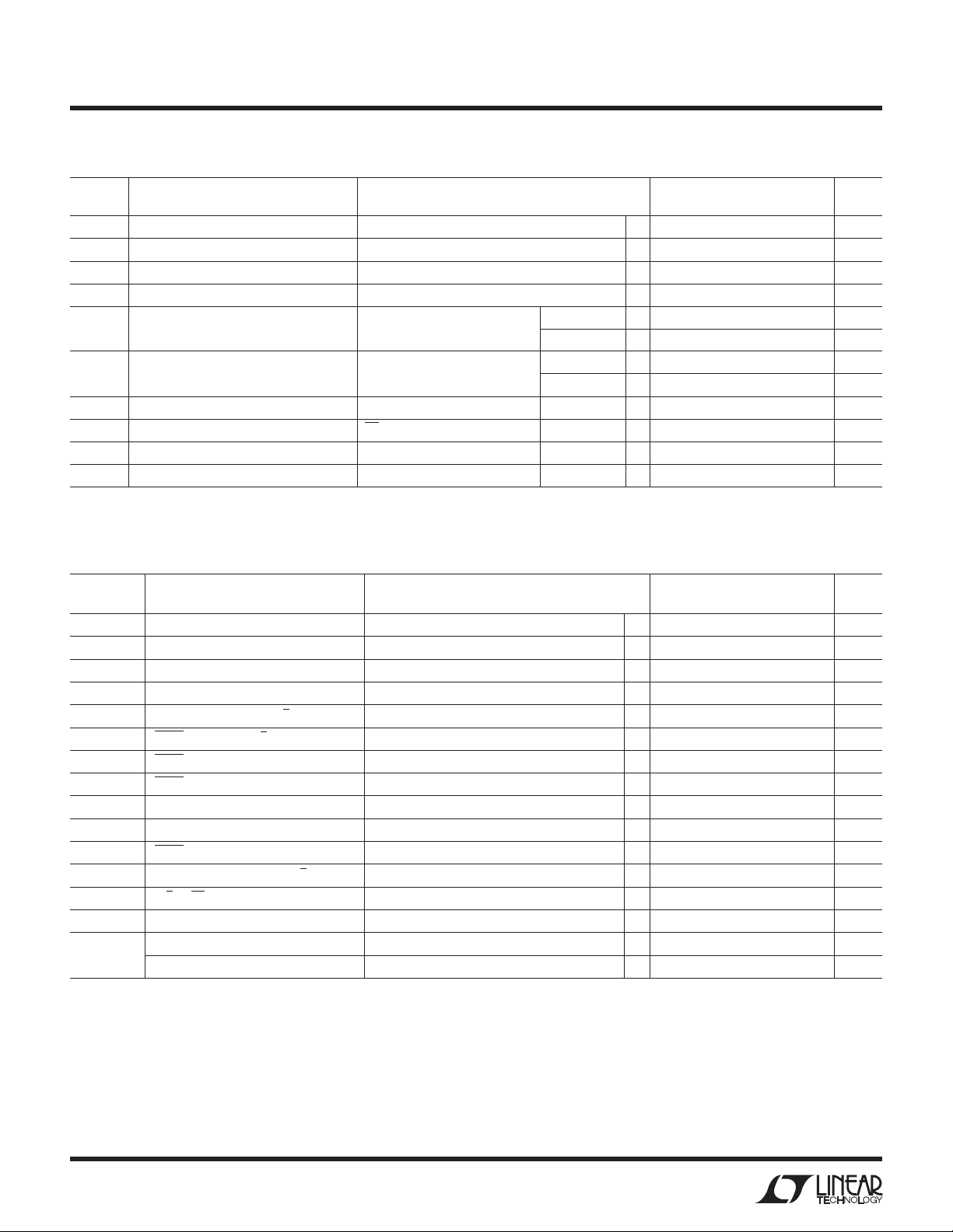
DIGITAL INPUTS AND DIGITAL OUTPUTS
operating temperature range, otherwise specifications are at TA = 25°C. (Note 5)
SYMBOL PARAMETER CONDITIONS MIN TYP MAX UNITS
V
IH
V
IL
I
IN
C
IN
V
OH
V
OL
I
OZ
C
OZ
I
SOURCE
I
SINK
High Level Input Voltage VDD = 5.25V ● 2.4 V
Low Level Input Voltage VDD = 4.75V ● 0.8 V
Digital Input Current VIN = 0V to V
Digital Input Capacitance 5pF
High Level Output Voltage VDD = 4.75V IO = –10µA 4.5 V
Low Level Output Voltage VDD = 4.75V IO = 160µA 0.05 V
Hi-Z Output Leakage D15 to D0 V
Hi-Z Output Capacitance D15 to D0 CS High (Note 9) ● 15 pF
Output Source Current V
Output Sink Current V
OUT
OUT
OUT
DD
= 0V to VDD, CS High ● ±10 µA
= 0V –10 mA
= V
DD
The ● indicates specifications which apply over the full
LTC1606/LTC1606A
● ±10 µA
IO = –200µA ● 4.0 V
IO = 1.6mA ● 0.10 0.4 V
10 mA
WU
TIMING CHARACTERISTICS
range, otherwise specifications are at TA = 25°C. (Note 5)
The ● indicates specifications which apply over the full operating temperature
LTC1606/LTC1606A
SYMBOL PARAMETER CONDITIONS MIN TYP MAX UNITS
f
SAMPLE(MAX)
t
CONV
t
ACQ
t
1
t
2
t
3
t
4
t
5
t
6
t
7
t
8
t
9
t
10
t
11
t
12
Maximum Sampling Frequency ● 250 kHz
Conversion Time ● 2.5 µs
Acquisition Time ● 1.5 µs
Convert Pulse Width (Note 11) ● 40 ns
Data Valid Delay After R/C↓ (Note 9) ● 2.5 µs
BUSY Delay from R/C↓ CL = 30pF ● 65 ns
BUSY Low ● 2.5 µs
BUSY Delay After End of Conversion 100 ns
Aperture Delay 40 ns
Bus Relinquish Time ● 15 50 ns
BUSY Delay After Data Valid ● 20 90 ns
Previous Data Valid After R/C↓ 2 µs
R/C to CS Setup Time (Notes 9, 10) ● 5ns
Time Between Conversions ● 4 µs
Bus Access CL = 30pF, (Notes 10) ● 15 60 ns
Byte Delay CL = 30pF, (Notes 9, 10) ● 15 60 ns
4
 Loading...