

Linear Technology LTC1605-2, LTC1605-1 Datasheet
1
LTC1605-1/LTC1605-2
Single Supply 16-Bit, 100ksps,
Sampling ADCs
The LTC®1605-1/LTC1605-2 are 100ksps, sampling
16-bit A/D converters that draw only 55mW (typical) from
a single 5V supply. These easy-to-use devices include a
sample-and-hold, precision reference, switched capacitor
successive approximation A/D and trimmed internal clock.
The LTC1605-1’s input range is 0V to 4V while the
LTC1605-2’s input range is ±4V. An external reference
can be used if greater accuracy over temperature is
needed.
The ADC has a microprocessor compatible, 16-bit or two
byte parallel output port. A convert start input and a data
ready signal (BUSY) ease connections to FIFOs, DSPs and
microprocessors.
■
Sample Rate: 100ksps
■
Complete 16-Bit Solution on a Single 5V Supply
■
Unipolar Input Range: 0V to 4V (LTC1605-1)
■
Bipolar Input Range: ±4V (LTC1605-2)
■
Power Dissipation: 55mW Typ
■
Signal-to-Noise Ratio: 86dB Typ
■
Operates with Internal or External Reference
■
Internal Synchronized Clock
■
28-Pin 0.3" PDIP and SSOP Packages
, LTC and LT are registered trademarks of Linear Technology Corporation.
■
Industrial Process Control
■
Multiplexed Data Acquisition Systems
■
High Speed Data Acquisition for PCs
■
Digital Signal Processing
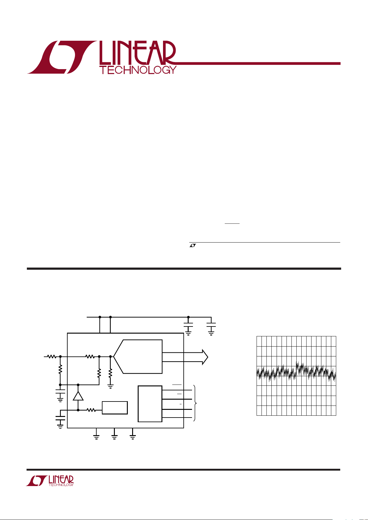
LTC1605-1 Low Power, 100kHz, 16-Bit Sampling ADC on 5V Supply
4k
4k
200Ω
2.5V
REFERENCE
20k 10k
16-BIT
SAMPLING ADC
D15 TO D0
33.2k
2.2µF
2.5V
2.5V
10µF 0.1µF
2.2µF
0V TO 4V
INPUT
V
IN
CAP
REF
AGND1
1
4
2
AGND25DGND
14
CONTROL
LOGIC AND
TIMING
BUSY
BYTE
CS
R/C
28 27
6 TO 13
15 TO 22
26
25
24
23
DIGITAL
CONTROL
SIGNALS
1605-1/2 TA01
16-BIT
OR 2 BYTE
PARALLEL
BUS
5V
V
DIGVANA
BUFFER
3
CODE
0
INL (LSBs)
65535
1605-1/2 TA02/G04
16384
32768
49152
2.0
1.5
1.0
0.5
0
–0.5
–1.0
–1.5
–2.0
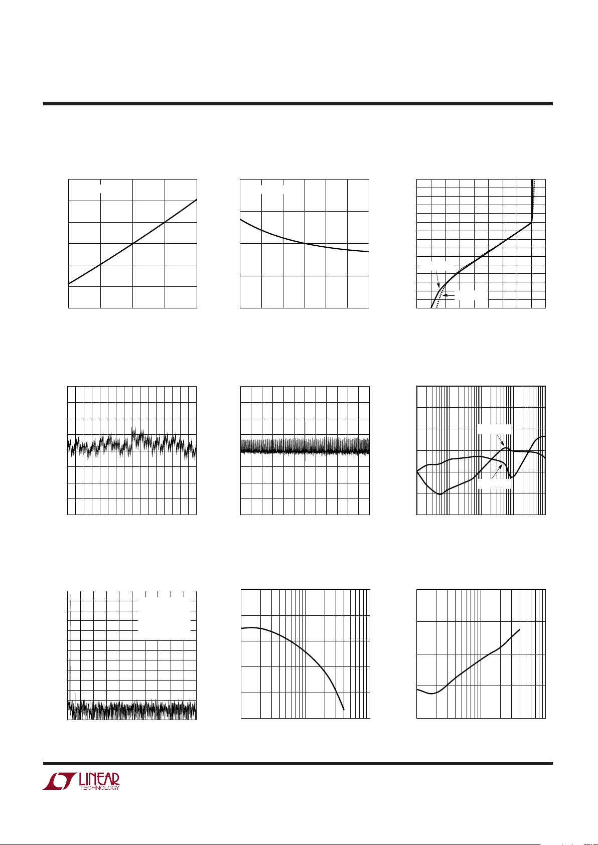
Typical INL Curve
FEATURES
DESCRIPTIO
U
APPLICATIO S
U
TYPICAL APPLICATIO
U
2
LTC1605-1/LTC1605-2
(Notes 1, 2)
V
ANA
.......................................................................... 7V
V
DIG
to V
ANA
........................................................... 0.3V
V
DIG
........................................................................... 7V
Ground Voltage Difference
DGND, AGND1 and AGND2 .............................. ±0.3V
Analog Inputs (Note 3)
VIN..................................................................... ±25V
CAP ............................ V
ANA
+ 0.3V to AGND2 – 0.3V
REF....................................Indefinite Short to AGND2
Momentary Short to V
ANA
Digital Input Voltage (Note 4) ........ V
DGND
– 0.3V to 10V
Digital Output Voltage........ V
DGND
– 0.3V to V
DIG
+ 0.3V
Power Dissipation.............................................. 500mW
Operating Ambient Temperature Range
LTC1605-1C/LTC1605-2C ....................... 0°C to 70°C
LTC1605-1I/LTC1605-2I .................... – 40°C to 85°C
Storage Temperature Range ................. –65°C to 150°C
Lead Temperature (Soldering, 10 sec).................. 300°C
Consult factory for Military grade parts.
ORDER PART
NUMBER
LTC1605-1CG
LTC1605-1IG
LTC1605-2CG
LTC1605-2IG
LTC1605-1CN
LTC1605-1IN
LTC1605-2CN
LTC1605-2IN
T
JMAX
= 125°C, θJA = 95°C/W (G)
T
JMAX
= 125°C, θJA = 130°C/W (N)
SYMBOL PARAMETER CONDITIONS MIN TYP MAX UNITS
V
IN
Analog Input Range (Note 9) 4.75V ≤ V
ANA
≤ 5.25V, 4.75V ≤ V
DIG
≤ 5.25V
LTC1605-1 ● 0 to 4 V
LTC1605-2
● ±4V
C
IN
Analog Input Capacitance 10 pF
R
IN
Analog Input Impedance 10 kΩ
The ● denotes the specifications which apply over the full operating temperature range, otherwise
PARAMETER CONDITIONS MIN TYP MAX UNITS
Resolution ● 16 Bits
No Missing Codes ● 15 Bits
Transition Noise 1 LSB
RMS
Integral Linearity Error (Note 7) ● ±3LSB
Zero Error Ext. Reference = 2.5V (Note 8) ● ±10 mV
Zero Error Drift ±2 ppm/°C
Full-Scale Error Drift ±7 ppm/°C
Full-Scale Error Ext. Reference = 2.5V (Notes 12, 13) ● ±0.50 %
Full-Scale Error Drift Ext. Reference = 2.5V ±2 ppm/°C
Power Supply Sensitivity
V
ANA
= V
DIG
= V
DD
VDD = 5V ±5% (Note 9) ±8LSB
The ● denotes the specifications which apply over the full operating
CO VERTER CHARACTERISTICS
U
A ALOG I PUT
UU
ABSOLUTE AXI U RATI GS
W
WW
U
PACKAGE/ORDER I FOR ATIO
UUW
1
2
3
4
5
6
7
8
9
10
11
12
13
14
28
27
26
25
24
23
22
21
20
19
18
17
16
15
V
IN
AGND1
REF
CAP
AGND2
D15 (MSB)
D14
D13
D12
D11
D10
D9
D8
DGND
V
DIG
V
ANA
BUSY
CS
R/C
BYTE
D0
D1
D2
D3
D4
D5
D6
D7
G PACKAGE
28-LEAD PLASTIC SSOP
N PACKAGE
28-LEAD PDIP
TOP VIEW
temperature range, otherwise specifications are at TA = 25°C. With external reference (Notes 5, 6).
specifications are at TA = 25°C. (Note 5)
3
LTC1605-1/LTC1605-2
SYMBOL PARAMETER CONDITIONS MIN TYP MAX UNITS
S/(N + D) Signal-to-(Noise + Distortion) Ratio 1kHz Input Signal (Note 14) 87 dB
10kHz Input Signal 85 dB
20kHz, –60dB Input Signal 30 dB
THD Total Harmonic Distortion 1kHz Input Signal, First 5 Harmonics – 101 dB
10kHz Input Signal, First 5 Harmonics – 92 dB
Peak Harmonic or Spurious Noise 1kHz Input Signal –101 dB
10kHz Input Signal –92 dB
Full-Power Bandwidth (Note 15) 275 kHz
Aperture Delay 40 ns
Aperture Jitter Sufficient to Meet AC Specs
Transient Response Full-Scale Step (Note 9) 2 µs
Overvoltage Recovery (Note 16) 150 ns
The ● denotes the specifications which apply over the full operating temperature range,
PARAMETER CONDITIONS MIN TYP MAX UNITS
V
REF
Output Voltage I
OUT
= 0 ● 2.470 2.500 2.520 V
V
REF
Output Tempco I
OUT
= 0 ±5 ppm/°C
Internal Reference Source Current 1 µA
External Reference Voltage for Specified Linearity (Notes 9, 10) 2.30 2.50 2.70 V
External Reference Current Drain Ext. Reference = 2.5V (Note 9) ● 100 µA
CAP Output Voltage I
OUT
= 0 2.50 V
SYMBOL PARAMETER CONDITIONS MIN TYP MAX UNITS
V
IH
High Level Input Voltage VDD = 5.25V ● 2.4 V
V
IL
Low Level Input Voltage VDD = 4.75V ● 0.8 V
I
IN
Digital Input Current VIN = 0V to V
DD
● ±10 µA
C
IN
Digital Input Capacitance 5pF
V
OH
High Level Output Voltage VDD = 4.75V IO = –10µA 4.5 V
IO = –200µA ● 4.0 V
V
OL
Low Level Output Voltage VDD = 4.75V IO = 160µA 0.05 V
IO = 1.6mA ● 0.10 0.4 V
I
OZ
Hi-Z Output Leakage D15 to D0 V
OUT
= 0V to VDD, CS High ● ±10 µA
C
OZ
Hi-Z Output Capacitance D15 to D0 CS High (Note 9) ● 15 pF
I
SOURCE
Output Source Current V
OUT
= 0V –10 mA
I
SINK
Output Sink Current V
OUT
= V
DD
10 mA
The ● denotes the specifications which apply over the
The ● denotes the specifications which apply over the
DY A IC ACCURACY
UW
I TER AL REFERE CE CHARACTERISTICS
UU U
DIGITAL I PUTS A D DIGITAL OUTPUTS
UU
otherwise specifications are at TA = 25°C. (Notes 5, 14)
full operating temperature range, otherwise specifications are at TA = 25°C. (Note 5)
full operating temperature range, otherwise specifications are at TA = 25°C. (Note 5)
4
LTC1605-1/LTC1605-2
The ● denotes the specifications which apply over the full operating temperature
SYMBOL PARAMETER CONDITIONS MIN TYP MAX UNITS
f
SAMPLE(MAX)
Maximum Sampling Frequency ● 100 kHz
t
CONV
Conversion Time ● 8 µs
t
ACQ
Acquisition Time ● 2 µs
t
1
Convert Pulse Width (Note 11) ● 40 ns
t
2
Data Valid Delay After R/C↓ (Note 9) ● 8 µs
t
3
BUSY Delay from R/C↓ CL = 50pF ● 65 ns
t
4
BUSY Low 8 µs
t
5
BUSY Delay After End of Conversion 220 ns
t
6
Aperture Delay 40 ns
t
7
Bus Relinquish Time ● 10 35 83 ns
t
8
BUSY Delay After Data Valid ● 50 200 ns
t
9
Previous Data Valid After R/C↓ 7.4 µs
t
10
R/C to CS Setup Time (Notes 9, 10) 10 ns
t
11
Time Between Conversions 10 µs
t
12
Bus Access and Byte Delay (Notes 9, 10) 10 83 ns
The ● denotes the specifications which apply over the full operating temperature
SYMBOL PARAMETER CONDITIONS MIN TYP MAX UNITS
V
DD
Positive Supply Voltage (Notes 9, 10) 4.75 5.25 V
I
DD
Positive Supply Current ● 11 16 mA
P
DIS
Power Dissipation 55 80 mW
Note 1: Absolute Maximum Ratings are those values beyond which the life
of a device may be impaired.
Note 2: All voltage values are with respect to ground with DGND, AGND1
and AGND2 wired together (unless otherwise noted).
Note 3: When these pin voltages are taken below ground or above V
ANA
=
V
DIG
= VDD, they will be clamped by internal diodes. This product can
handle input currents of greater than 100mA below ground or above V
DD
without latch-up.
Note 4: When these pin voltages are taken below ground, they will be
clamped by internal diodes. This product can handle input currents of
90mA below ground without latchup. These pins are not clamped to V
DD
.
Note 5: VDD = 5V, f
SAMPLE
= 100kHz, tr = tf = 5ns unless otherwise
specified.
Note 6: Linearity, offset and full-scale specifications apply for a V
IN
input
with respect to ground.
Note 7: Integral nonlinearity is defined as the deviation of a code from a
straight line passing through the actual end points of the transfer curve.
The deviation is measured from the center of the quantization band.
Note 8: Zero error for the LTC1605-1 is the voltage measured from
0.5LSB when the output code flickers between 0000 0000 0000 0000
and 0000 0000 0000 0001. Zero error for the LTC1605-2 is the voltage
measured from –0.5LSB when the output code flickers between 0000
0000 0000 0000 and 1111 1111 1111 1111.
Note 9: Guaranteed by design, not subject to test.
Note 10: Recommended operating conditions.
Note 11: With CS low the falling R/C edge starts a conversion. If R/C
returns high at a critical point during the conversion it can create small
errors. For best results ensure that R/C returns high within 3µs after the
start of the conversion.
Note 12: As measured with fixed resistors shown in Figure 4. Adjustable to
zero with external potentiometer.
Note 13: Full-scale error is the untrimmed deviation from ideal last code
transition, divided by the full-scale range and includes the effect of offset
error.
Note 14: All specifications in dB are referred to a full-scale 4V input for the
LTC1605-1 and to ±4V input for the LTC1605-2.
Note 15: Full-power bandwidth is defined as full-scale input frequency at
which a signal-to-(noise + distortion) degrades to 60dB or 10 bits of
accuracy.
Note 16: Recovers to specified performance after (±20V) input
overvoltage for the LTC1605-1 and ±15V for the LTC1605-2.
TI I G CHARACTERISTICS
WU
POWER REQUIRE E TS
WU
range, otherwise specifications are at TA = 25°C. (Note 5)
range, otherwise specifications are at TA = 25°C. (Note 5)
5
LTC1605-1/LTC1605-2
TYPICAL PERFOR A CE CHARACTERISTICS
UW
SUPPLY VOLTAGE (V)
4.50
9.5
SUPPLY CURRENT (mA)
10.0
10.5
11.0
11.5
12.0
12.5
4.75 5.00 5.25 5.50
1605-1/2 G01
f
SAMPLE
= 100kHz
TEMPERATURE (°C)
–50
10.0
POWER SUPPLY CURRENT (mA)
10.5
11.0
11.5
12.0
–25 0 25 50
1605-1/2 G02
75 100
f
SAMPLE
= 100kHz
LOAD CURRENT (mA)
CHANGE IN CAP VOLTAGE (V)
0.04
0.02
0
–0.02
–0.04
–0.06
–0.08
–0.10
–60 –40 –20 0
1605-1/2 G03
–70–80 –50 –30 –10 10
LTC1605-1
LTC1605-2
CODE
0
DNL (LSB)
65535
1605-1/2 G05
16384
32768
49152
2.0
1.5
1.0
0.5
0
–0.5
–1.0
–1.5
–2.0
FREQUENCY (kHz)
0
MAGNITUDE (dB)
1605-1/2 G07/F11
5 10 15 20 25 30 35 40 45 50
0
–10
–20
–30
–40
–50
–60
–70
–80
–90
–100
–110
–120
–130
f
SAMPLE
= 100kHz
f
IN
= 1kHz
SINAD = 87dB
THD = 101.1dB
SNR = 87.2dB
INPUT FREQUENCY (kHz)
1
SINAD (dB)
90
88
86
84
82
80
10 100
1605-1/2 G08
INPUT FREQUENCY (kHz)
1
TOTAL HARMONIC DISTORTION (dB)
–70
–80
–90
–100
–110
10 100
1605-1/2 G09
Supply Current vs Supply Voltage Supply Current vs Temperature
Change in CAP Voltage vs
Load Current
Typical INL Curve Typical DNL Curve
Power Supply Feedthrough
vs Ripple Frequency
LTC1605-2 Nonaveraged
4096-Point FFT Plot
SINAD vs Input Frequency
(LTC1605-2)
Total Harmonic Distortion vs
Input Frequency (LTC1605-2)
CODE
0
INL (LSBs)
65535
1605-1/2 TA02/G04
16384
32768
49152
2.0
1.5
1.0
0.5
0
–0.5
–1.0
–1.5
–2.0
RIPPLE FREQUENCY (Hz)
POWER SUPPLY FEEDTHROUGH (dB)
–20
–30
–40
–50
–60
–70
–80
100 10k 100k 1M
LTXXXX GXX
1k
LTC1605-2
LTC1605-1
6
LTC1605-1/LTC1605-2
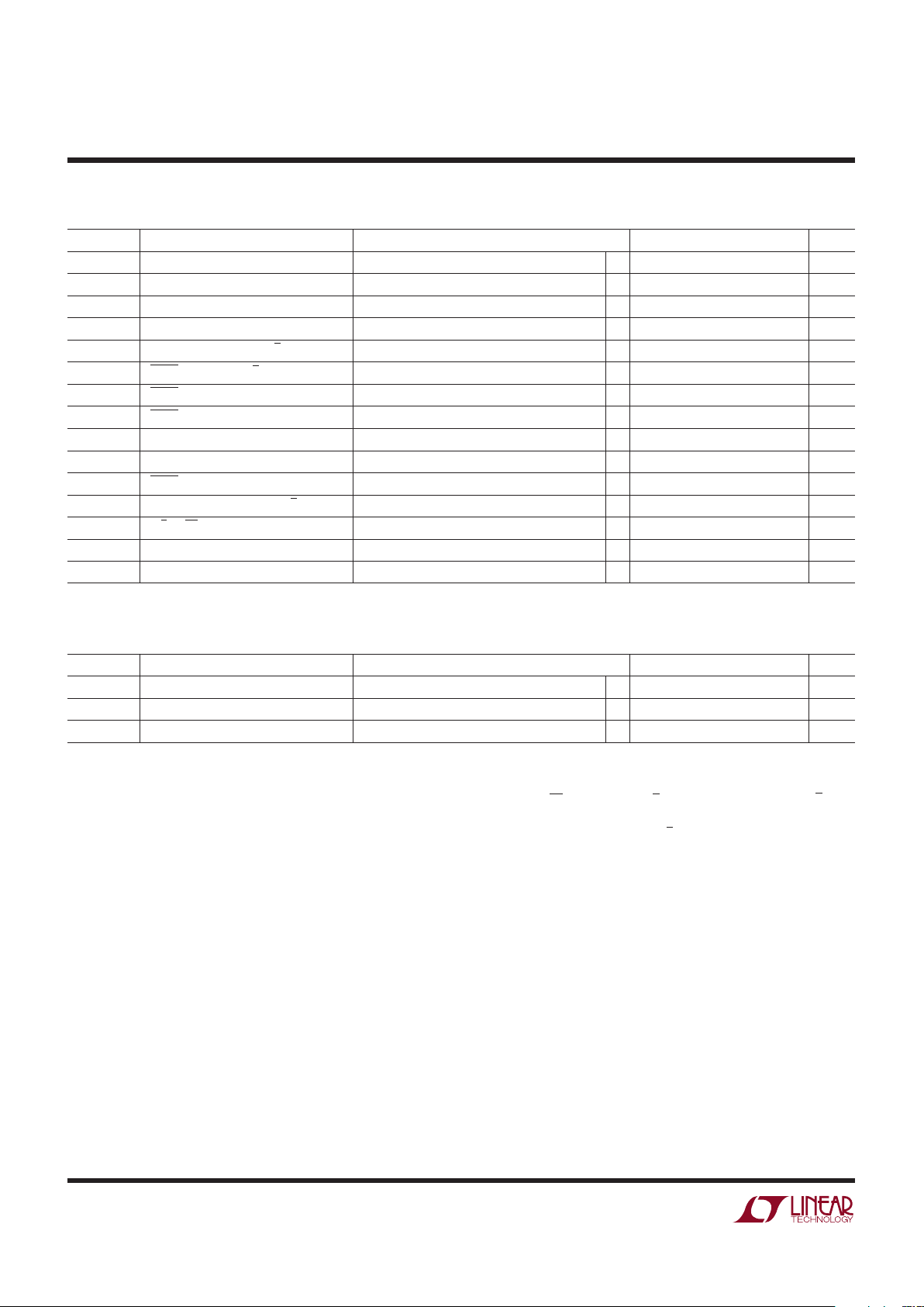
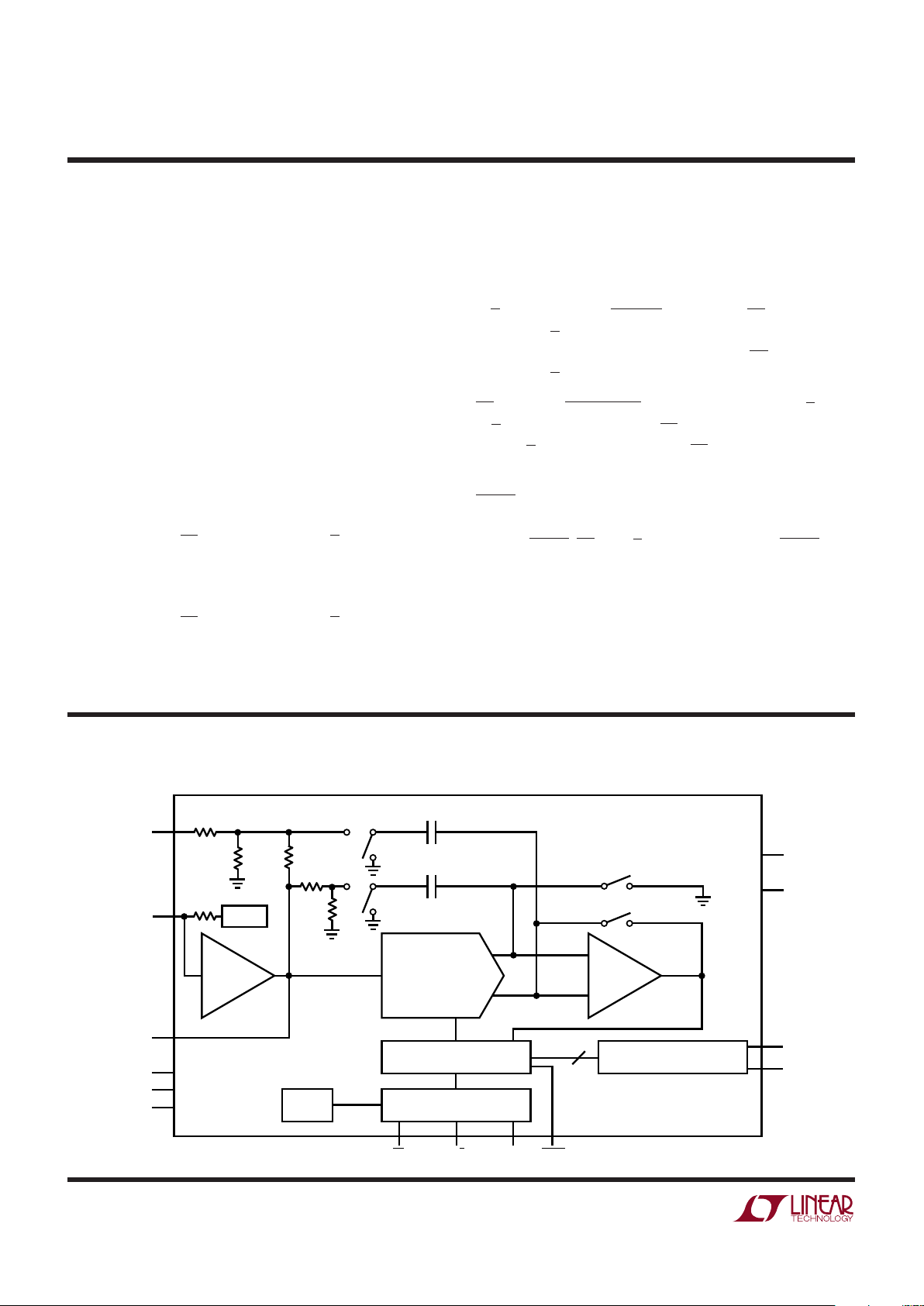
16-BIT CAPACITIVE DAC
COMPREF BUF
2.5V REF
CAP
(2.5V)
C
SAMPLE
C
SAMPLE
•
•
•
D15
D0
BUSY
CONTROL LOGIC
R/C BYTE
INTERNAL
CLOCK
CS
ZEROING SWITCHES
V
DIG
V
ANA
V
IN
REF
AGND1
AGND2
DGND
16
1605-1/2 BD
+
–
SUCCESSIVE APPROXIMATION
REGISTER
OUTPUT LATCHES
4k
4k
6K*
20k
3.75k*
10k
OPEN*
*RESISTOR VALUES FOR THE LTC1605-2
VIN (Pin 1): Analog Input. Connect through a 200Ω
resistor to the analog input. Full-scale input range is 0V
to 4V for the LTC1605-1 and ±4V for the LTC1605-2.
AGND1 (Pin 2): Analog Ground. Tie to analog ground
plane.
REF (Pin 3): 2.5V Reference Output. Bypass with 2.2µF
tantalum capacitor. Can be driven with an external reference.
CAP (Pin 4): Reference Buffer Output. Bypass with 2.2µF
tantalum capacitor.
AGND2 (Pin 5): Analog Ground. Tie to analog ground
plane.
D15 to D8 (Pins 6 to 13): Three-State Data Outputs.
Hi-Z state when CS is high or when R/C is low.
DGND (Pin 14): Digital Ground.
D7 to D0 (Pins 15 to 22): Three-State Data Outputs.
Hi-Z state when CS is high or when R/C is low.
BYTE (Pin 23): Byte Select. With BYTE low, data will be
output with Pin 6 (D15) being the MSB and Pin 22 (D0)
PIN FUNCTIONS
UUU
being the LSB. With BYTE high the upper eight bits and
the lower eight bits will be switched. The MSB is output
on Pin 15 and bit 8 is output on Pin 22. Bit 7 is output on
Pin 6 and the LSB is output on Pin 13.
R/C (Pin 24): Read/Convert Input. With CS low, a falling
edge on R/C puts the internal sample-and-hold into the
hold state and starts a conversion. With CS low, a rising
edge on R/C enables the output data bits.
CS (Pin 25): Chip Select. Internally OR’d with R/C. With
R/C low, a falling edge on CS will initiate a conversion.
With R/C high, a falling edge on CS will enable the output
data.
BUSY (Pin 26): Output Shows Converter Status. It is low
when a conversion is in progress. Data valid on the rising
edge of BUSY. CS or R/C must be high when BUSY rises
or another conversion will start without time for signal
acquisition.
V
ANA
(Pin 27): 5V Analog Supply. Bypass to ground with
a 0.1µF ceramic and a 10µF tantalum capacitor.
V
DIG
(Pin 28): 5V Digital Supply. Connect directly to
Pin␣ 27.
FU CTIO AL BLOCK DIAGRA
UU
W
 Loading...