

FEATURES
LTC1594/LTC1598
4- and 8-Channel,
Micropower Sampling
12-Bit Serial I/O A/D Converters
U
DESCRIPTION
■
12-Bit Resolution
■
Auto Shutdown to 1nA
■
Low Supply Current: 320µA Typ
■
Guaranteed ±3/4LSB Max DNL
■
Single Supply 5V Operation
(3V Versions Available: LTC1594L/LTC1598L)
■
Multiplexer: 4-Channel MUX (LTC1594)
8-Channel MUX (LTC1598)
■
Separate MUX Output and ADC Input Pins
■
MUX and ADC May Be Controlled Separately
■
Sampling Rate: 16.8ksps
■
I/O Compatible with QSPI, SPI and MICROWIRETM, etc.
■
Small Package: 16-Pin Narrow SO (LTC1594)
24-Pin SSOP (LTC1598)
U
APPLICATIONS
■
Pen Screen Digitizing
■
Battery-Operated Systems
■
Remote Data Acquisition
■
Isolated Data Acquisition
■
Battery Monitoring
■
Temperature Measurement
The LTC®1594/LTC1598 are micropower, 12-bit sampling
A/D converters that feature 4- and 8-channel multiplexers,
respectively. They typically draw only 320µA of supply
current when converting and automatically power down to
a typical supply current of 1nA between conversions. The
LTC1594 is available in a 16-pin SO package and the
LTC1598 is packaged in a 24-pin SSOP. Both operate on
a 5V supply. The 12-bit, switched-capacitor, successive
approximation ADCs include a sample-and-hold.
On-chip serial ports allow efficient data transfer to a wide
range of microprocessors and microcontrollers over three
or four wires. This, coupled with micropower consumption, makes remote location possible and facilitates transmitting data through isolation barriers.
The circuit can be used in ratiometric applications or with
an external reference. The high impedance analog inputs
and the ability to operate with reduced spans (to 1.5V full
scale) allow direct connection to sensors and transducers
in many applications, eliminating the need for gain stages.
, LTC and LT are registered trademarks of Linear Technology Corporation.
MICROWIRE is a trademark of National Semiconductor Corporation.
U
TYPICAL APPLICATION
24µW, 4-Channel, 12-Bit ADC Samples at 200Hz and Runs Off a 5V Supply
OPTIONAL
ADC FILTER
ANALOG
INPUTS
0V TO 5V
RANGE
20
21
22
23
24
1
2
3
8 COM
CH0
CH1
CH2
CH3
CH4
CH5
CH6
CH7
1k
1µF
8-CHANNEL
MUX
18 17 16 15, 19
ADCINMUXOUT
+
V
REFVCC
12-BIT
SAMPLING
ADC
CSADC
CSMUX
–
GND
4, 9
CLK
D
IN
D
OUT
NC
NC
1594/98 TA01
10
6
5, 14
7
11
12
13
5V
1µF
SERIAL DATA LINK
MICROWIRE AND
SPI COMPATABLE
MPU
Supply Current vs Sample Rate
1000
TA = 25°C
= 5V
V
CC
= 5V
V
REF
= 320kHz
f
CLK
100
10
SUPPLY CURRENT (µA)
1
0.1
1 10 100
SAMPLE FREQUENCY (kHz)
1594/98 TA02
1
LTC1594/LTC1598
WW
W
U
ABSOLUTE MAXIMUM RATINGS
(Notes 1, 2)
Supply Voltage (VCC) to GND................................... 12V
Voltage
Analog Reference .................... –0.3V to (VCC + 0.3V)
Analog Inputs .......................... –0.3V to (VCC + 0.3V)
Digital Inputs .........................................– 0.3V to 12V
Digital Output .......................... –0.3V to (VCC + 0.3V)
U
W
PACKAGE/ORDER INFORMATION
ORDER PART
NUMBER
TOP VIEW
1
CH0
2
CH1
3
CH2
4
CH3
5
ADCIN
6
V
REF
7
COM
8
GND
16-LEAD PLASTIC SO
T
JMAX
16
15
14
13
12
11
10
9
S PACKAGE
= 125°C, θJA = 120°C/ W
V
CC
MUXOUT
D
IN
CSMUX
CLK
V
CC
D
OUT
CSADC
LTC1594CS
LTC1594IS
Power Dissipation.............................................. 500mW
Operating Temperature Range
LTC1594CS/LTC1598CG ......................... 0°C to 70°C
LTC1594IS/LTC1598IG ..................... –40°C to 85°C
Storage Temperature Range ................. –65°C to 150°C
Lead Temperature (Soldering, 10 sec).................. 300°C
U
ORDER PART
NUMBER
LTC1598CG
LTC1598IG
1
CH5
2
CH6
3
CH7
4
GND
5
CLK
6
CSMUX
7
D
IN
8
COM
9
GND
10
CSADC
11
D
OUT
12
NC
24-LEAD PLASTIC SSOP
T
JMAX
TOP VIEW
24
23
22
21
20
19
18
17
16
15
14
13
G PACKAGE
= 150°C, θJA = 110°C/ W
CH4
CH3
CH2
CH1
CH0
V
CC
MUXOUT
ADCIN
V
REF
V
CC
CLK
NC
Consult factory for Military grade parts.
WW
RECOM ENDED OPERATING CONDITIONS
UU
UU
(Note 5)
SYMBOL PARAMETER CONDITIONS MIN TYP MAX UNITS
V
CC
f
CLK
t
CYC
t
hDI
t
suCS
t
suDI
t
WHCLK
t
WLCLK
t
WHCS
t
WLCS
Supply Voltage (Note 3) 4.5 5.5 V
Clock Frequency VCC = 5V (Note 4) 320 kHz
Total Cycle Time f
= 320kHz 60 µs
CLK
Hold Time, DIN After CLK↑ VCC = 5V 150 ns
Setup Time CS↓ Before First CLK↑ (See Operating Sequence) VCC = 5V 1 µs
Setup Time, DIN Stable Before CLK↑ VCC = 5V 400 ns
CLK High Time VCC = 5V 1 µs
CLK Low Time VCC = 5V 1 µs
CS High Time Between Data Transfer Cycles f
CS Low Time During Data Transfer f
= 320kHz 16 µs
CLK
= 320kHz 44 µs
CLK
2
LTC1594/LTC1598
UW
CONVERTER AND MULTIPLEXER CHARACTERISTICS
PARAMETER CONDITIONS MIN TYP MAX MIN TYP MAX UNITS
Resolution (No Missing Codes) ● 12 12 Bits
Integral Linearity Error (Note 6) ● ±3 ±3LSB
Differential Linearity Error ● ±3/4 ±1LSB
Offset Error ● ±3 ±3LSB
Gain Error ● ±8 ±8LSB
REF Input Range (Notes 7, 8) 1.5V to V
Analog Input Range (Notes 7, 8) –0.05V to VCC + 0.05V V
MUX Channel Input Leakage Current Off Channel ● ±200 ±200 nA
MUXOUT Leakage Current Off Channel ● ±200 ±200 nA
ADCIN Input Leakage Current (Note 9) ● ±1 ±1 µA
U
(Note 5)
LTC1594CS/LTC1598CG LTC1594IS/LTC1598IG
+ 0.05V V
CC
UW
DYNAMIC ACCURACY
SYMBOL PARAMETER CONDITIONS MIN TYP MAX UNITS
S/(N + D) Signal-to-Noise Plus Distortion Ratio 1kHz Input Signal 71 dB
THD Total Harmonic Distortion (Up to 5th Harmonic) 1kHz Input Signal – 78 dB
SFDR Spurious-Free Dynamic Range 1kHz Input Signal 80 dB
Peak Harmonic or Spurious Noise 1kHz Input Signal – 80 dB
(Note 5) f
SMPL
= 16.8kHz
U
DIGITAL AND DC ELECTRICAL CHARACTERISTICS
SYMBOL PARAMETER CONDITIONS MIN TYP MAX UNITS
V
IH
V
IL
I
IH
I
IL
V
OH
V
OL
I
OZ
I
SOURCE
I
SINK
R
REF
I
REF
I
CC
High Level Input Voltage VCC = 5.25V ● 2.6 V
Low Level Input Voltage VCC = 4.75V ● 0.8 V
High Level Input Current VIN = V
Low Level Input Current VIN = 0V ● –2.5 µA
High Level Output Voltage VCC = 4.75V, IO = 10µA ● 4.0 4.64 V
Low Level Output Voltage VCC = 4.75V, IO = 1.6mA ● 0.4 V
Hi-Z Output Leakage CS = High ● ±3 µA
Output Source Current V
Output Sink Current V
Reference Input Resistance CS = V
Reference Current CS = V
Supply Current CS = VCC, CLK = VCC, DIN = V
CC
VCC = 4.75V, IO = 360µA ● 2.4 4.62 V
= 0V –25 mA
OUT
= V
OUT
CC
IH
CS = V
IL
CC
≥ 760µs, f
t
CYC
t
≥ 60µs, f
CYC
≥ 760µs, f
t
CYC
t
≥ 60µs, f
CYC
≤ 25kHz 90 µA
CLK
≤ 320kHz ● 90 140 µA
CLK
≤ 25kHz 320 µA
CLK
≤ 320kHz ● 320 690 µA
CLK
CC
(Note 5)
● 2.5 µA
45 mA
5000 MΩ
55 kΩ
● 0.001 2.5 µA
● 0.001 ±5 µA
3
LTC1594/LTC1598
TEMPERATURE (°C)
–55
92.0
REFERENCE CURRENT (µA)
92.5
93.5
94.0
94.5
–15
25
45 125
1594/98 G03
93.0
–35 5
65
85
105
95.0
VCC = V
REF
= 5V
f
SMPL
= 16.8kHz
f
CLK
= 320kHz
AC CHARACTERISTICS
(Note 5)
SYMBOL PARAMETER CONDITIONS MIN TYP MAX UNITS
t
SMPL
f
SMPL(MAX)
t
CONV
t
dDO
t
dis
t
en
t
hDO
t
f
t
r
t
ON
t
OFF
t
OPEN
C
IN
Analog Input Sample Time See Figure 1 in Applications Information 1.5 CLK Cycles
Maximum Sampling Frequency See Figure 1 in Applications Information ● 16.8 kHz
Conversion Time See Figure 1 in Applications Information 12 CLK Cycles
Delay Time, CLK↓ to D
Delay Time, CS↑ to D
Delay Time, CLK↓ to D
Time Output Data Remains Valid After CLK↓ C
D
Fall Time See Test Circuits ● 50 150 ns
OUT
D
Rise Time See Test Circuits ● 50 150 ns
OUT
Data Valid See Test Circuits ● 250 600 ns
OUT
Hi-Z See Test Circuits ● 135 300 ns
OUT
Enabled See Test Circuits ● 75 200 ns
OUT
= 100pF 230 ns
LOAD
Enable Turn-On Time See Figure 1 in Applications Information ● 260 700 ns
Enable Turn-Off Time See Figure 2 in Applications Information ● 100 300 ns
Break-Before-Make Interval ● 35 160 ns
Input Capacitance Analog Inputs On-Channel 20 pF
Off-Channel 5 pF
Digital Input 5 pF
The ● denotes specifications which apply over the full operating
temperature range.
Note 1: Absolute Maximum Ratings are those values beyond which the life
of a device may be impaired.
Note 2: All voltage values are with respect to GND.
Note 3: These devices are specified at 5V. Consult factory for 3V
specified devices (LTC1594L/LTC1598L).
Note 4: Increased leakage currents at elevated temperatures cause the S/H
to droop, therefore it is recommended that f
≥ 75kHz at 70°C and f
f
CLK
Note 5: VCC = 5V, V
REF
≥ 1kHz at 25°C.
CLK
= 5V and CLK = 320kHz unless otherwise specified.
≥ 160kHz at 85°C,
CLK
CSADC and CSMUX pins are tied together during the test.
Note 6: Linearity error is specified between the actual end points of the
A/D transfer curve.
Note 7: Two on-chip diodes are tied to each reference and analog input
which will conduct for reference or analog input voltages one diode drop
below GND or one diode drop above V
bias of either diode for 4.5V ≤ V
. This spec allows 50mV forward
CC
≤ 5.5V. This means that as long as the
CC
reference or analog input does not exceed the supply voltage by more than
50mV, the output code will be correct. To achieve an absolute 0V to 5V
input voltage range, it will therefore require a minimum supply voltage of
4.950V over initial tolerance, temperature variations and loading.
Note 8: Recommended operating condition.
Note 9: Channel leakage current is measured after the channel selection.
W
U
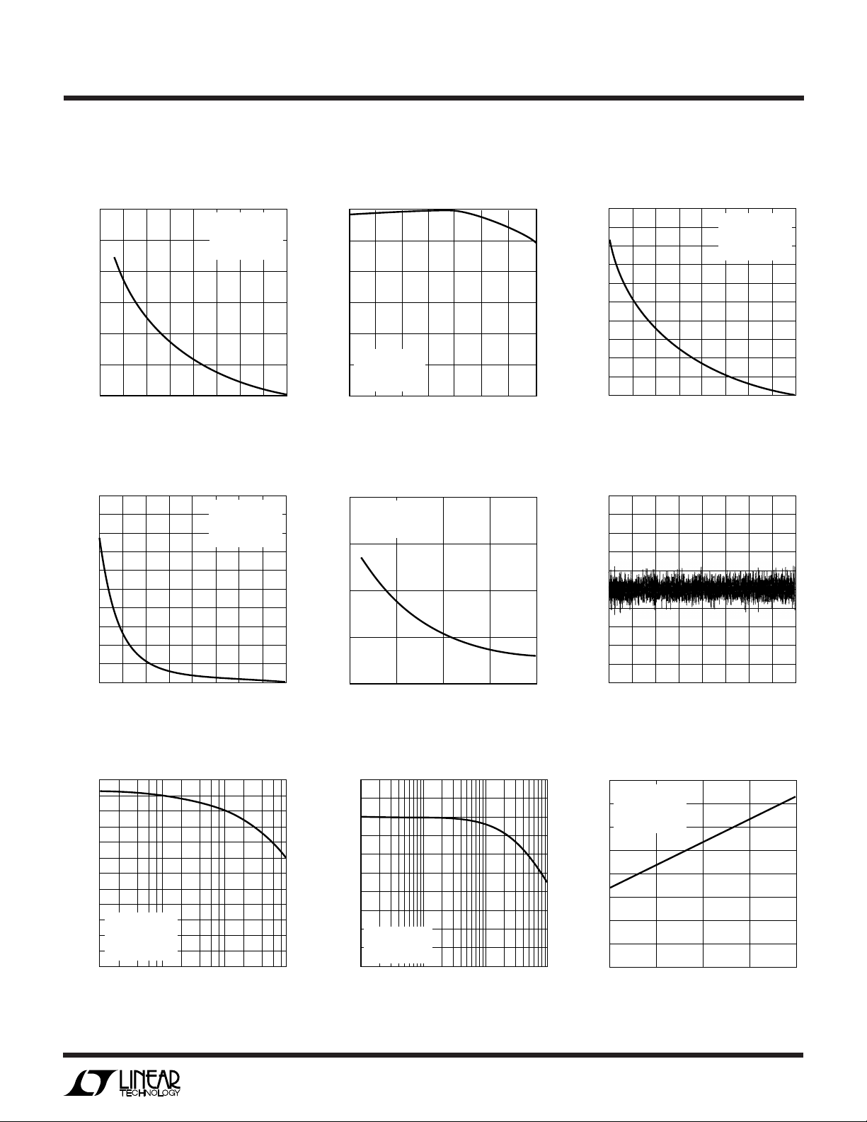
TYPICAL PERFORMANCE CHARACTERISTICS
Supply Current vs Sample Rate
1000
TA = 25°C
= 5V
V
CC
= 5V
V
REF
= 320kHz
f
CLK
100
10
SUPPLY CURRENT (µA)
1
0.1
4
1 10 100
SAMPLE FREQUENCY (kHz)
1594/98 G01
Supply Current vs Temperature
450
TA = 25°C
= V
= 5V
V
CC
REF
= 320kHz
f
CLK
400
350
300
SUPPLY CURRENT (µA)
250
200
f
SMPL
–35 5
–55
= 16.8kHz
–15
TEMPERATURE (°C)
25
85
45 125
105
65
1594/98 G02
Reference Current vs Temperature
W
0
–0.05
–0.15
–0.20
–0.25
–0.30
–0.50
–0.35
–0.10
–0.40
–0.45
REFERENCE VOLTAGE (V)
1.0
CHANGE IN LINEARITY (LSB)
2.0 3.0
4.0
5.0
1594/98 G06
1.5 2.5
3.5
4.5
TA = 25°C
V
CC
= 5V
f
CLK
= 320kHz
f
SMPL
= 16.8kHz
INPUT LEVEL (dB)
–40
0
SIGNAL-TO-NOISE PLUS DISTORTION (dB)
20
10
40
30
60
50
80
70
–30 –20
1594/98 G12
–10 0
TA = 25°C
V
CC
= V
REF =
5V
f
IN
= 1kHz
f
SMPL
= 16.8kHz
CODE
0
DIFFERENTIAL NONLINEARITY ERROR (LBS)
–1.0
–0.8
–0.6
–0.4
–0.2
0.4
0.6
0.8
1.0
0.2
0.0
2048
1594/98 G09
4096
U
TYPICAL PERFORMANCE CHARACTERISTICS
LTC1594/LTC1598
Change in Offset
vs Reference Voltage
3.0
)
REF
2.5
2.0
1.5
1.0
0.5
CHANGE IN OFFSET (LSB = 1/4096 V
0
1.0
2.0 3.0
1.5 2.5
REFERENCE VOLTAGE (V)
Change in Gain
vs Reference Voltage
–10
–9
–8
–7
–6
–5
–4
–3
CHANGE IN GAIN (LSB)
–2
–1
0
1.0
2.0 3.0
1.5 2.5
REFERENCE VOLTAGE (V)
TA = 25°C
= 5V
V
CC
= 320kHz
f
CLK
f
SMPL
4.0
3.5
TA = 25°C
= 5V
V
CC
= 320kHz
f
CLK
f
SMPL
4.0
3.5
= 16.8kHz
4.5
1594/98 G04
= 16.8kHz
4.5
1594/98 G07
5.0
5.0
Change in Offset vs Temperature
0
–0.5
–1.0
–1.5
–2.0
CHANGE IN OFFSET (LSB)
–2.5
–3.0
VCC = V
f
f
–55
= 5V
REF
= 320kHz
CLK
= 16.8kHz
SMPL
–15 25
–35 5
TEMPERATURE (°C)
Peak-to-Peak ADC Noise
vs Reference Voltage
2.0
TA = 25°C
V
= 5V
CC
f
= 320kHz
CLK
1.5
1.0
ADC NOISE IN LBSs
0.5
0
1
2
REFERENCE VOLTAGE (V)
3
Change in Linearity
vs Reference Voltage
65
45
85
1594/98 G05
Differential Nonlinearity vs Code
4
5
1594/98 G08
Effective Bits and S/(N + D)
vs Input Frequency
12
11
10
9
8
7
6
5
4
3
TA = 25°C
V
CC
2
f
CLK
EFFECTIVE NUMBER OF BITS (ENOBs)
1
f
SMPL
0
1
= 5V
= 320kHz
= 16.8kHz
10 100 1000
INPUT FREQUENCY (kHz)
1594/98 G10
Spurious Free Dynamic Range
vs Frequency
74
68
62
56
50
44
38
100
90
80
70
60
50
40
30
20
TA = 25°C
= V
V
CC
10
SPURIOUS FREE DYNAMIC RANGE (dB)
f
SMPL
0
1
5V
REF =
= 16.8kHz
10 100 1000
INPUT FREQUENCY (kHz)
1594/98 G11
S/(N + D) vs Input Level
5
LTC1594/LTC1598
SOURCE RESISTANCE (Ω)
10 100 1000
1594/98 G18
10.1 10000
100
S & H ACQUISITION TIME (ns)
1000
10000
TA = 25°C
V
CC
= V
REF
= 5V
+INPUT
COM
R
SOURCE
+
V
IN
W
U
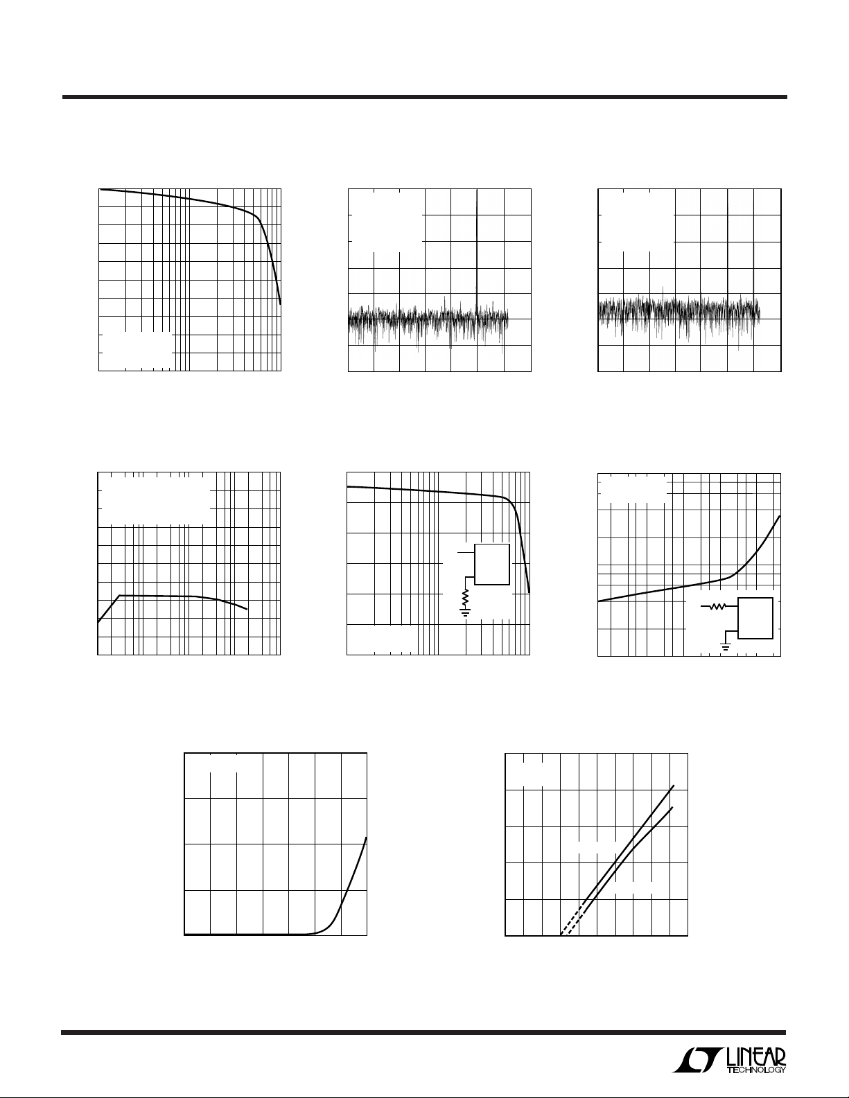
TYPICAL PERFORMANCE CHARACTERISTICS
Attenuation vs Input Frequency
0
10
20
30
40
50
60
ATTENUATION (%)
70
80
TA = 25°C
= V
V
CC
90
f
SMPL
100
110
5V
REF =
= 16.8kHz
INPUT FREQUENCY (kHz)
100 1000 10000
Power Supply Feedthrough
vs Ripple Frequency
0
TA = 25°C
= 5V (V
V
CC
= 5V
V
REF
= 320kHz
f
CLK
–50
FEEDTHROUGH (dB)
–100
1 100 1000 10000
= 20mV)
RIPPLE
10
RIPPLE FREQUENCY (kHz)
1594/98 G13
1594/98 G16
4096 Point FFT Plot
0
TA = 25°C
= V
CC
REF
= 5kHz
IN
= 320kHz
CLK
= 12.5kHz
SMPL
12
= 5V
35
FREQUENCY (kHz)
V
–20
f
f
–40
f
–60
–80
MAGNITUDE (dB)
–100
–120
–140
0
Maximum Clock Frequency
vs Source Resistance
360
300
240
180
120
CLOCK FREQUENCY (kHz)
60
TA = 25°C
= V
V
0
0.1
= 5V
CC
REF
SOURCE RESISTANCE (kΩ)
Intermodulation Distortion
0
TA = 25°C
V
–20
f
1
f
2
–40
f
SMPL
–60
–80
MAGNITUDE (dB)
–100
–120
467
1594/98 G14
–140
0
Sample-and-Hold Acquisition Time
vs Source Resistance
+INPUT
V
IN
COM
–
R
SOURCE
110
1594/98 G17
= V
CC
REF =
= 5kHz
= 6kHz
= 12.5kHz
12
5V
467
35
FREQUENCY (kHz)
1594/98 G15
6
Minimum Clock Frequency for
0.1LSB Error vs Temperature
320
VCC = V
240
160
80
CLOCK FREQUENCY (kHz)
0
–55
–35
REF
–15
= 5V
5
25 45 65 85
TEMPERATURE (°C)
1594/98 G19
Input Channel Leakage Current
vs Temperature
1000
VCC = 5V
V
= 5V
REF
100
10
ON CHANNEL
1
20
OFF CHANNEL
60
40 80
LEAKAGE CURRENT (nA)
0.1
0.01
–60
–40
0
–20
TEMPERATURE (°C)
100
120
1594/98 G20
140

UUU
PIN FUNCTIONS
LTC1594
LTC1594/LTC1598
CH0 (Pin 1): Analog Multiplexer Input.
CH1 (Pin 2): Analog Multiplexer Input.
CH2 (Pin 3): Analog Multiplexer Input.
CH3 (Pin 4): Analog Multiplexer Input.
ADCIN (Pin 5): ADC Input. This input is the positive analog
input to the ADC. Connect this pin to MUXOUT for normal
operation.
V
(Pin 6): Reference Input. The reference input defines
REF
the span of the ADC.
COM (Pin 7): Negative Analog Input. This input is the
negative analog input to the ADC and must be free of noise
with respect to GND.
GND (Pin 8): Analog Ground. GND should be tied directly
to an analog ground plane.
CSADC (Pin 9): ADC Chip Select Input. A logic high on this
input powers down the ADC and three-states D
low on this input enables the ADC to sample the selected
channel and start the conversion. For normal operation
drive this pin in parallel with CSMUX.
OUT
. A logic
D
(Pin 10): Digital Data Output. The A/D conversion
OUT
result is shifted out of this output.
VCC (Pin 11): Power Supply Voltage. This pin provides
power to the ADC. It must be bypassed directly to the
analog ground plane.
CLK (Pin 12): Shift Clock. This clock synchronizes the
serial data transfer to both MUX and ADC.
CSMUX (Pin 13): MUX Chip Select Input. A logic high on
this input allows the MUX to receive a channel address. A
logic low enables the selected MUX channel and connects
it to the MUXOUT pin for A/D conversion. For normal
operation, drive this pin in parallel with CSADC.
DIN (Pin 14): Digital Data Input. The multiplexer address
is shifted into this input.
MUXOUT (Pin 15): MUX Output. This pin is the output of
the multiplexer. Tie to ADCIN for normal operation.
VCC (Pin 16): Power Supply Voltage. This pin should be
tied to Pin 11.
LTC1598
CH5 (Pin 1): Analog Multiplexer Input.
CH6 (Pin 2): Analog Multiplexer Input.
CH7 (Pin 3): Analog Multiplexer Input.
GND (Pin 4): Analog Ground. GND should be tied directly
to an analog ground plane.
CLK (Pin 5): Shift Clock. This clock synchronizes the serial
data transfer to both MUX and ADC. It also determines the
conversion speed of the ADC.
CSMUX (Pin 6): MUX Chip Select Input. A logic high on
this input allows the MUX to receive a channel address. A
logic low enables the selected MUX channel and connects
it to the MUXOUT pin for A/D conversion. For normal
operation, drive this pin in parallel with CSADC.
DIN (Pin 7): Digital Data Input. The multiplexer address is
shifted into this input.
COM (Pin 8): Negative Analog Input. This input is the
negative analog input to the ADC and must be free of noise
with respect to GND.
GND (Pin 9): Analog Ground. GND should be tied directly
to an analog ground plane.
CSADC (Pin 10): ADC Chip Select Input. A logic high on
this input deselects and powers down the ADC and threestates D
sample the selected channel and start the conversion. For
normal operation drive this pin in parallel with CSMUX.
D
OUT
result is shifted out of this output.
NC (Pin 12): No Connection.
NC (Pin 13): No Connection.
CLK (Pin 14): Shift Clock. This input should be tied to Pin 5.
. A logic low on this input enables the ADC to
OUT
(Pin 11): Digital Data Output. The A/D conversion
7
LTC1594/LTC1598
UUU
PIN FUNCTIONS
VCC (Pin 15): Power Supply Voltage. This pin provides
power to the A/D Converter. It must be bypassed directly
to the analog ground plane.
V
(Pin 16): Reference Input. The reference input de-
REF
fines the span of the ADC.
ADCIN (Pin 17): ADC Input. This input is the positive
analog input to the ADC. Connect this pin to MUXOUT for
normal operation.
MUXOUT (Pin 18): MUX Output. This pin is the output of
the multiplexer. Tie to ADCIN for normal operation.
W
BLOCK DIAGRA S
LTC1594
15 5 6 16
+
SAMPLING
–
V
12-BIT
ADC
GND
REFVCC
8
CSADC
CSMUX
CLK
D
D
OUT
LTC1594
9
13
12
14
IN
10
1
CH0
2
CH1
3
CH2
4
CH3
7 COM
ADCINMUXOUT
4-CHANNEL
MUX
VCC (Pin 19): Power Supply Voltage. This pin should be
tied to Pin 15.
CH0 (Pin 20): Analog Multiplexer Input.
CH1 (Pin 21): Analog Multiplexer Input.
CH2 (Pin 22): Analog Multiplexer Input.
CH3 (Pin 23): Analog Multiplexer Input.
CH4 (Pin 24): Analog Multiplexer Input.
LTC1598
18 17 16 15, 19
+
SAMPLING
–
V
12-BIT
ADC
GND
REFVCC
4, 9
CSADC
CSMUX
CLK
D
D
OUT
NC
NC
LTC1598
1594/98 BD
10
6
5, 14
7
IN
11
12
13
20
21
22
23
24
1
2
3
8 COM
CH0
CH1
CH2
CH3
CH4
CH5
CH6
CH7
ADCINMUXOUT
8-CHANNEL
MUX
TEST CIRCUITS
Load Circuit for t
D
OUT
8
1.4V
3k
dDO
100pF
, tr and t
TEST POINT
f
1594/98 TC01
Voltage Waveforms for D
D
OUT
t
r
Rise and Fall Times, tr, t
OUT
t
f
1594/98 TC02
f
V
OH
V
OL
 Loading...