

Linear Technology LTC1334 Datasheet
FEATURES
LTC1334
Single 5V RS232/RS485
Multiprotocol Transceiver
U
DESCRIPTIO
■
Four RS232 Transceivers or Two RS485
Transceivers on One Chip
■
Operates from a Single 5V Supply
■
Withstands Repeated ±10kV ESD Pulses
■
Uses Small Charge Pump Capacitors: 0.1µF
■
Low Supply Current: 8mA Typical
■
10µA Supply Current in Shutdown
■
Self-Testing Capability in Loopback Mode
■
Power-Up/Down Glitch-Free Outputs
■
Driver Maintains High Impedance in Three-State,
Shutdown or with Power Off
■
Thermal Shutdown Protection
■
Receiver Inputs Can Withstand ±25V
U
APPLICATIO S
■
Low Power RS485/RS422/RS232/EIA562 Interface
■
Software-Selectable Multiprotocol Interface Port
■
Cable Repeaters
■
Level Translators
The LTC®1334 is a low power CMOS
ceiver featuring two
reconfigurable interface ports. It can
bidirectional trans-
be configured as two RS485 differential ports, as two dual
RS232 single-ended ports or as one RS485 differential
port and one dual RS232 single-ended port. An onboard
charge pump requires four 0.1µF capacitors to generate
boosted positive and negative supplies, allowing the RS232
drivers to meet the RS232 ±5V output swing requirement
with only a single 5V supply. A shutdown mode reduces
the ICC supply current to 10µA.
The RS232 transceivers are in full compliance with RS232
specifications. The RS485 transceivers are in full compliance with RS485 and RS422 specifications. All interface
drivers feature short-circuit and thermal shutdown protection. An enable pin allows RS485 driver outputs to be
forced into high impedance, which is maintained even
when the outputs are forced beyond supply rails or power
is off. Both driver outputs and receiver inputs feature
±10kV ESD protection. A loopback mode allows the driver
outputs to be connected back to the receiver inputs for
diagnostic self-test.
, LTC and LT are registered trademarks of Linear Technology Corporation.
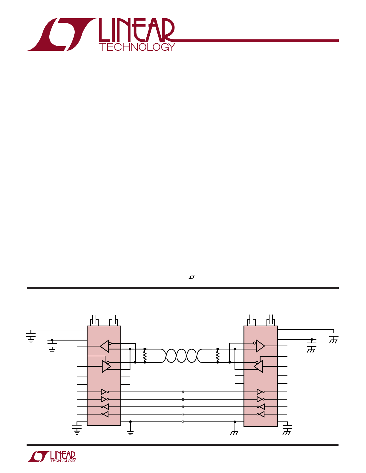
TYPICAL APPLICATIO
12
3
LTC1334
DR IN
DR IN
DR IN
26
24
23
22
21
5V
20
5V
19
18
17
16
15
V
CC1
5V
RX OUT
DR ENABLE
RX OUT
RX OUT
U
2728
LTC1334
4
5
6
7
8
9
11
10
13
12
14
120Ω
5V
0V
ALL CAPACITORS: 0.1µF MONOLITHIC CERAMIC TYPE
RS485 INTERFACE
4000-FT 24-GAUGE TWISTED PAIR
RS232 INTERFACE
120Ω
13
12
11
10
9
5V
8
0V
4
5
6
7
14
212827
3
26
17
18
19
21
20
24
25
22
23
15
RX OUT
DR ENABLE
DR IN
5V
5V
RX OUT
RX OUT
DR IN
DR IN
V
CC2
5V
LTC1334 • TA01
1
LTC1334
A
S
(Note 1)
W
O
LUTEXI TIS
A
WUW
U
ARB
G
Supply Voltage (VCC) ............................................. 6.5V
Input Voltage
Drivers ................................... –0.3V to (VCC + 0.3V)
Receivers ............................................. – 25V to 25V
ON/OFF, LB, SEL1, SEL2 ........ –0.3V to (VCC + 0.3V)
Output Voltage
Drivers ................................................. – 18V to 18V
Receivers ............................... –0.3V to (VCC + 0.3V)
Short-Circuit Duration
Output ........................................................ Indefinite
VDD, VEE, C1+, C1–, C2+, C2–.......................... 30 sec
Operating Temperature Range
Commercial........................................... 0°C to 70°C
Industrial............................................ –40°C to 85°C
Storage Temperature Range ................ –65°C to 150°C
Lead Temperature (Soldering, 10 sec)................ 300°C
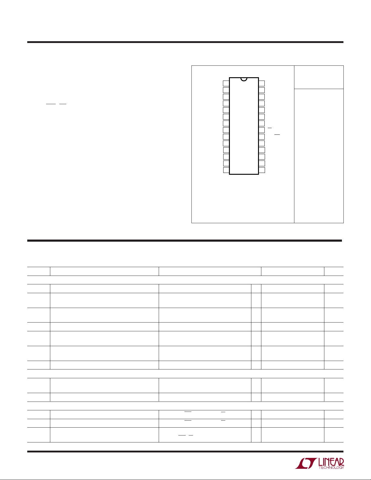
PACKAGE
+
1
C1
–
2
C1
3
V
DD
4
A1
5
B1
6
Y1
7
Z1
8
SEL1
9
SEL2
10
Z2
11
Y2
12
B2
13
A2
14
GND
G PACKAGE
28-LEAD PLASTIC SSOP
28-LEAD PLASTIC SO WIDE
T
= 125°C, θJA = 90°C/W (G)
JMAX
T
= 125°C, θJA = 56°C/W (NW)
JMAX
T
= 125°C, θJA = 85°C/W (SW)
JMAX
/
O
RDER I FOR ATIO
TOP VIEW
28-LEAD PDIP WIDE
SW PACKAGE
28
C2
27
C2
26
V
CC
25
R
B1
24
R
A1
23
DZ1/DE1
22
D
Y1
21
LB
20
ON/OFF
19
D
Y2
18
DZ2/DE2
17
R
A2
16
R
B2
15
V
EE
NW PACKAGE
+
–
ORDER PART
LTC1334CG
LTC1334CNW
LTC1334CSW
LTC1334IG
LTC1334ISW
WU
U
NUMBER
Consult factory for Military grade parts.
DC ELECTRICAL CHARACTERISTICS
The ● denotes specifications which apply over the full operating
temperature range, otherwise specifications are at TA = 25°C. VCC = 5V, C1 = C2 = C3 = C4 = 0.1µF (Notes 2, 3)
SYMBOL PARAMETER CONDITIONS MIN TYP MAX UNITS
RS485 Driver (SEL1 = SEL2 = High)
V
OD1
V
OD2
∆V
OD
V
OC
∆VOC Change in Magnitude of Driver Common Mode Figure 1, R = 27Ω or R = 50Ω ● 0.2 V
I
OSD
I
OZD
RS232 Driver (SEL1 = SEL2 = Low)
V
O
I
OSD
Driver Inputs and Control Inputs
V
IH
V
IL
I
IN
Differential Driver Output Voltage (Unloaded) IO = 0 ● 6V
Differential Driver Output Voltage (With Load) Figure 1, R = 50Ω (RS422) ● 2.0 6 V
Figure 1, R = 27Ω (RS485) ● 1.5 6 V
Change in Magnitude of Driver Differential Figure 1, R = 27Ω or R = 50Ω ● 0.2 V
Output Voltage for Complementary Output States
Driver Common Mode Output Voltage Figure 1, R = 27Ω or R = 50Ω ● 3V
Output Voltage for Complementary Output States
Driver Short-Circuit Current –7V ≤ VO ≤ 12V, VO = High ● 35 250 mA
–7V ≤ V
Three-State Output Current (Y, Z) –7V ≤ VO ≤ 12V ● ±5 ±500 µA
Output Voltage Swing Figure 4, RL = 3k, Positive ● 5 6.5 V
Figure 4, R
Output Short-Circuit Current VO = 0V ● ±60 mA
Input High Voltage D, DE, ON/OFF, SEL1, SEL2, LB ● 2V
Input Low Voltage D, DE, ON/OFF, SEL1, SEL2, LB ● 0.8 V
Input Current D, SEL1, SEL2 ● ±10 µA
DE, ON/OFF, LB
≤ 12V, VO = Low (Note 4) ● 10 250 mA
O
= 3k, Negative ● –5 –6.5 V
L
● –4 –15 µA
2
LTC1334
DC ELECTRICAL CHARACTERISTICS
The ● denotes specifications which apply over the full operating
temperature range, otherwise specifications are at TA = 25°C. VCC = 5V, C1 = C2 = C3 = C4 = 0.1µF (Notes 2, 3)
SYMBOL PARAMETER CONDITIONS MIN TYP MAX UNITS
RS485 Receiver (SEL1 = SEL2 = High)
V
TH
∆V
TH
I
IN
R
IN
RS232 Receiver (SEL1 = SEL2 = Low)
V
TH
∆V
TH
R
IN
Receiver Output
V
OH
V
OL
I
OSR
I
OZR
R
OB
Power Supply Generator
V
DD
V
EE
Power Supply
I
CC
Differential Input Threshold Voltage –7V ≤ VCM ≤ 12V, LTC1334C ● –0.2 0.2 V
–7V ≤ V
≤ 7V, LTC1334I ● –0.3 0.3 V
CM
Input Hysteresis VCM = 0V 70 mV
Input Current (A, B) VIN = –7V ● – 0.8 mA
= 12V ● 1.0 mA
V
IN
Input Resistance –7V ≤ VIN ≤ 12V ● 12 24 kΩ
Receiver Input Threshold Voltage Input Low Threshold ● 0.8 V
Input High Threshold
● 2.4 V
Receiver Input Hysteresis 0.6 V
Receiver Input Resistance VIN = ±10V 3 5 7 kΩ
Receiver Output High Voltage IO = –3mA, VIN = 0V, SEL1 = SEL2 = Low ● 3.5 4.6 V
Receiver Output Low Voltage IO = 3mA, VIN = 3V, SEL1 = SEL2 = Low ● 0.2 0.4 V
Short-Circuit Current 0V ≤ VO ≤ V
CC
● 785mA
Three-State Output Current ON/OFF = Low ● ±10 µA
Inactive “B” Output Pull-Up Resistance (Note 5) ON/OFF = High, SEL1 = SEL2 = High 50 kΩ
VDD Output Voltage No Load, ON/OFF = High 8.5 V
= –10mA, ON/OFF = High 7.6 V
I
DD
VEE Output Voltage No Load, ON/OFF = High – 7.7 V
= 10mA, ON/OFF = High –6.9 V
I
EE
VCC Supply Current No Load, SEL1 = SEL2 = High ● 825 mA
No Load Shutdown, ON/OFF = 0V
● 10 100 µA
AC ELECTRICAL CHARACTERISTICS
The ● denotes specifications which apply over the full operating
temperature range, otherwise specifications are at TA = 25°C. VCC = 5V, C1 = C2 = C3 = C4 = 0.1µF (Notes 2, 3)
SYMBOL PARAMETER CONDITIONS MIN TYP MAX UNITS
RS232 Mode (SEL1 = SEL2 = Low)
SR Slew Rate Figure 4, RL = 3k, CL = 15pF ● 30 V/µs
t
t
t
t
t
T
PLH
PHL
PLH
PHL
Figure 4, R
Transition Time Figure 4, RL = 3k, CL = 2500pF ● 0.22 1.9 3.1 µs
Driver Input to Output Figures 4, 9, RL = 3k, CL = 15pF ● 0.6 4 µs
Driver Input to Output Figures 4, 9, RL = 3k, CL = 15pF ● 0.6 4 µs
Receiver Input to Output Figures 5, 10 ● 0.3 6 µs
Receiver Input to Output Figures 5, 10 ● 0.4 6 µs
= 3k, CL = 1000pF ● 4V/µs
L
RS485 Mode (SEL1 = SEL2 = High)
t
PLH
t
PHL
t
SKEW
tr, t
f
Driver Input to Output Figures 2, 6, RL = 54Ω, CL = 100pF ● 20 40 70 ns
Driver Input to Output Figures 2, 6, RL = 54Ω, CL = 100pF ● 20 40 70 ns
Driver Output to Output Figures 2, 6, RL = 54Ω, CL = 100pF ● 515 ns
Driver Rise and Fall Time Figures 2, 6, RL = 54Ω, CL = 100pF ● 31540 ns
3
LTC1334
AC ELECTRICAL CHARACTERISTICS
The ● denotes specifications which apply over the full operating
temperature range, otherwise specifications are at TA = 25°C. VCC = 5V, C1 = C2 = C3 = C4 = 0.1µF (Notes 2, 3)
SYMBOL PARAMETER CONDITIONS MIN TYP MAX UNITS
RS485 Mode (SEL1 = SEL2 = High)
t
ZL
t
ZH
t
LZ
t
HZ
t
PLH
t
PHL
t
SKEW
Note 1: Absolute Maximum Ratings are those values beyond which the
safety of the device cannot be guaranteed.
Note 2: All currents into device pins are positive; all currents out of device
pins are negative. All voltages are referenced to device ground unless
otherwise specified.
Note 3: All typicals are given at VCC = 5V, C1 = C2 = C3 = C4 = 0.1µF
and T
Driver Enable to Output Low Figures 3, 7, CL = 100pF, S1 Closed ● 50 90 ns
Driver Enable to Output High Figures 3, 7, CL = 100pF, S2 Closed ● 50 90 ns
Driver Disable from Low Figures 3, 7, CL = 15pF, S1 Closed ● 50 90 ns
Driver Disable from High Figures 3, 7, CL = 15pF, S2 Closed ● 60 90 ns
Receiver Input to Output Figures 2, 8, RL = 54Ω, CL = 100pF ● 20 60 140 ns
Receiver Input to Output Figures 2, 8, RL = 54Ω, CL = 100pF ● 20 70 140 ns
Differential Receiver Skew, t
PLH
– t
Figures 2, 8, R
PHL
= 54Ω, CL = 100pF 10 ns
L
Note 4: Short-circuit current for RS485 driver output low state folds back
above VCC. Peak current occurs around VO = 3V.
Note 5: The “B” RS232 receiver output is disabled in RS485 mode
(SEL1 = SEL2 = high). The unused output driver goes into a high
impedance mode and has a resistor to VCC. See Applications Information
section for more details.
= 25°C.
A
W
U
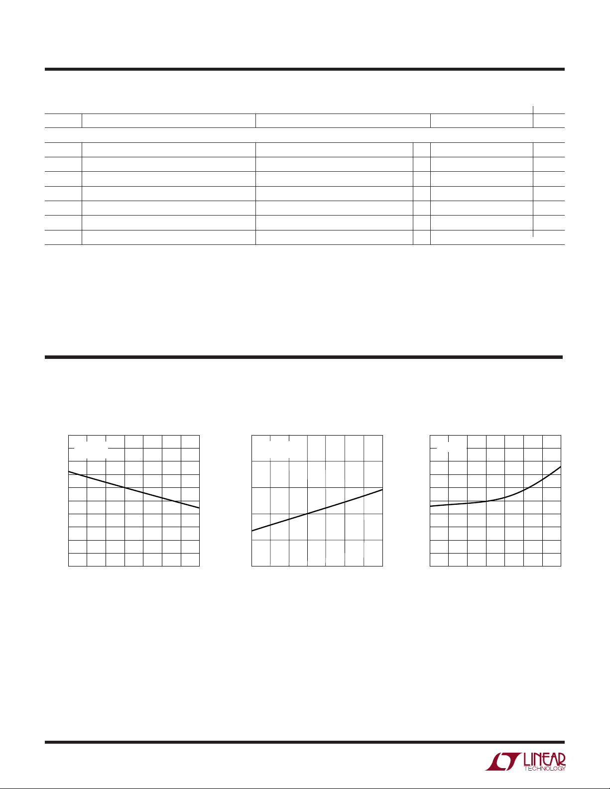
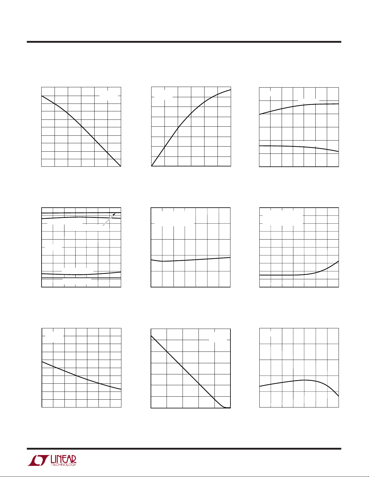
TYPICAL PERFORMANCE CHARACTERISTICS
Receiver Output High Voltage
vs Temperature
5.0
I
= 3mA
OUT
4.9
4.8
4.7
4.6
4.5
4.4
4.3
OUTPUT VOLTAGE (V)
4.2
4.1
4.0
–50
= 5V
V
CC
–25
0
TEMPERATURE (°C)
50
25
75
100
LTC1334 • TPC01
125
Receiver Output Low Voltage
vs Temperature
0.5
I
= 3mA
OUT
V
= 5V
CC
0.4
0.3
0.2
OUTPUT VOLTAGE (V)
0.1
0
–50
0
–25
TEMPERATURE (°C)
50
25
75
100
LTC1334 • TPC02
125
RS485 Receiver Skew
t
– t
PLH
VCC = 5V
–25
PHL
0
TEMPERATURE (°C)
20
18
16
14
12
10
TIME (ns)
8
6
4
2
0
–50
vs Temperature
50
25
75
100
LTC1334 • TPC03
125
4
W
TEMPERATURE (°C)
–50
INPUT THRESHOLD VOLTAGE (V)
2.0
1.8
1.6
1.4
1.2
1.0
0.8
25 75
LTC1334 • TPC06
–25 0
50 100 125
INPUT HIGH
INPUT LOW
VCC = 5V
TEMPERATURE (°C)
–50
SUPPLY CURRENT (mA)
10
9
8
7
6
5
4
3
2
1
0
0
50
75
LTC1334 • TPC09
–25
25
100
125
VCC = 5V
NO LOAD
SEL 1 = SEL 2 = HIGH
U
TYPICAL PERFORMANCE CHARACTERISTICS
LTC1334
Receiver Output Current
vs Output High Voltage
20
18
16
14
12
10
8
6
OUTPUT CURRENT (mA)
4
2
0
2.0
2.5
3.5 4.0
3.0
OUTPUT VOLTAGE (V)
Charge Pump Output Voltage
vs Temperature
10
8
VDD (–10mA LOAD)
6
4
2
VCC = 5V
0
–2
–4
OUTPUT VOLTAGE (V)
–6
–8
–10
–50
–25
VDD (NO LOAD)
VEE (10mA LOAD)
VEE (NO LOAD)
0
TEMPERATURE (°C)
50
25
TA = 25°C
V
CC
75
= 5V
4.5
LTC1334 • TPC04
100
LTC1334 • TPC07
125
5.0
Receiver Output Current
vs Output Low Voltage
40
TA = 25°C
= 5V
V
35
CC
30
25
20
15
OUTPUT CURRENT (mA)
10
5
0
0 0.5
1.0 2.01.5
OUTPUT VOLTAGE (V)
Supply Current
vs Temperature (RS485)
25
VCC = 5V
NO LOAD
20
SEL 1 = SEL 2 = HIGH
15
10
SUPPLY CURRENT (mA)
5
0
–50
–25
25
0
TEMPERATURE (°C)
RS232 Receiver Input Threshold
Voltage vs Temperature
2.5
3.0
LTC1334 • TPC05
Supply Current
vs Temperature (RS232)
50
75
100
LTC1334 • TPC08
125
RS485 Driver Differential Output
Voltage vs Temperature
2.6
RL = 54Ω
2.5
2.4
2.3
2.2
2.1
2.0
1.9
1.8
DIFFERENTIAL OUTPUT VOLTAGE (V)
1.7
1.6
= 5V
V
CC
–50
–25
25
50
0
TEMPERATURE (°C)
75
100
LTC1334 • TPC10
125
RS485 Driver Differential Output
Current vs Output Voltage
70
60
50
40
30
20
10
DIFFERENTIAL OUTPUT CURRENT (mA)
0
12 5
0
DIFFERENTIAL OUTPUT VOLTAGE (V)
34
TA = 25°C
= 5V
V
CC
LTC1334 • TPC11
RS485 Driver Skew
vs Temperature
15
VCC = 5V
12
9
TIME (µs)
6
3
0
–50
–25
0
TEMPERATURE (°C)
50
25
75
100
LTC1334 • TPC12
5
125
 Loading...