

FEATURES
■
Fast Charge Nickel-Cadmium, Nickel-Metal-Hydride,
Lithium Ion or Lead-Acid Batteries under µP Control
■
Flexible Current Regulation:
– Programmable 111kHz PWM Current Regulator
with Built-In PFET Driver
– PFET Current Gating for Use with External Current
Regulator or Current Limited Transformer
■
Discharge Mode
■
Measures Battery Voltage, Battery Temperature and
Ambient Temperature with Internal 10-Bit ADC
■
Battery Voltage, Temperature and Charge Time
Fault Protection
■
Built-In Voltage Regulator and Programmable
Battery Attenuator
■
Easy-to-Use 3- or 4-Wire Serial µP Interface
■
Accurate Gas Gauge Function
■
Wide Supply Range: VDD = 4.5V to 16V
■
Can Charge Batteries with Voltages Greater Than V
■
Can Charge Batteries from Charging Supplies Greater
Than V
■
Digital Input Pins Are High Impedance in
DD
Shutdown Mode
U
APPLICATIONS
■
System Integrated Battery Charger
LTC1325
Microprocessor-Controlled
Battery Management System
U
DESCRIPTION
The LTC®1325 provides the core of a flexible, cost-effective solution for an integrated battery management system. The monolithic CMOS chip controls the fast charging
of nickel-cadmium, nickel-metal-hydride, lead-acid or
lithium batteries under microprocessor control. The device features a programmable 111kHz PWM constant
current source controller with built-in FET driver, 10-bit
ADC, internal voltage regulator, discharge-before-charge
controller, programmable battery voltage attenuator and
an easy-to-use serial interface.
The chip may operate in one of five modes: power shutdown, idle, discharge, charge or gas gauge. In power
shutdown the supply current drops to 30µ A and in the idle
mode, an ADC reading may be made without any switching
noise affecting the accuracy of the measurement. In the
discharge mode, the battery is discharged by an external
DD
transistor while the battery is being monitored by the
LTC1325 for fault conditions. The charge mode is terminated by the µP while monitoring any combination of
battery voltage and temperature, ambient temperature
and charge time. The LTC1325 also monitors the battery
for fault conditions before and during charging. In the gas
gauge mode the LTC1325 allows the total charge leaving
the battery to be calculated.
, LTC and LT are registered trademarks of Linear Technology Corporation.
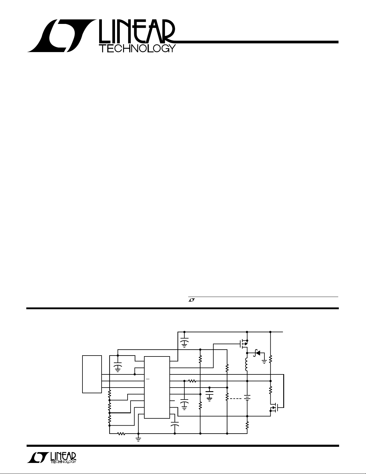
TYPICAL APPLICATION
MPU
(e.g. 8051)
p1.4
p1.3
p1.2
+
R1
R2
R3
R4
U
Battery Charger for up to 8 NiCd or NiMH Cells
+
C2
10µF
LTC1325
C
REG
4.7µF
1
REG
2
D
OUT
3
D
IN
4
CS
5
CLK
6
LTF
7
MCV
8
HTF
9
GND
V
PGATE
DIS
V
BAT
T
BAT
T
AMB
V
SENSE
FILTER
18
DD
17
16
15
14
13
+
12
IN
11
10
C
F
1µF
100Ω
C
22µF
REG
R13
THERM 2
C1
0.1µF
IRF9730
R5
THERM 1
V
DD
R
R
4.5V TO 16V
TRK
DIS
LTC1325 • TA01
P1
1N6818
L1
62µH
BAT
R
SENSE
D1
IRFZ34
N1
1
LTC1325
WW
W
ABSOLUTE MAXIMUM RATINGS
(Notes 1, 2)
VDD to GND............................................................. 17V
All Other Pins................................ –0.3V to VDD + 0.3V
Operating Temperature Range ..................... 0°C to 70°C
Storage Temperature Range ................. –65°C to 150°C
Lead Temperature (Soldering, 10 sec)..................300°C
U
U
W
PACKAGE/ORDER INFORMATION
TOP VIEW
1
REG
2
D
OUT
3
D
IN
4
CS
5
CLK
6
LTF
7
MCV
8
HTF
9
GND
N PACKAGE
18-LEAD PDIP
T
= 125°C, θJA = 75°C/ W (N)
JMAX
T
= 125°C, θJA = 100°C/ W (SW)
JMAX
18
V
DD
17
PGATE
16
DIS
15
V
BAT
14
T
BAT
13
T
AMB
12
V
IN
11
SENSE
10
FILTER
SW PACKAGE
18-LEAD PLASTIC SO WIDE
ORDER PART
NUMBER
LTC1325CN
LTC1325CSW
Consult factory for Industrial and Military grade parts.
ELECTRICAL CHARACTERISTICS
VDD = 12V ±5%, TA = 25°C, unless otherwise noted.
SYMBOL PARAMETER CONDITIONS MIN TYP MAX UNITS
V
DD
I
DD
I
PD
V
REG
LD
REG
LI
REG
TC
REG
V
DAC
V
HYST
V
OS
V
BATR
V
BATP
V
EDV
V
LTF
V
HTF
A
GG
V
OS(GG)
R
F
TOL
V
IL
V
IH
I
IL
I
IH
, V
BATD
VDD Supply Voltage ● 4.5 16 V
VDD Supply Current All TTL Inputs = 0V or 5V, No Load on REG ● 1200 2000 µA
VDD Supply Current Power-Down Mode, All TTL Inputs = 0V or 5V ● 30 50 µA
Regulator Output Voltage No Load ● 3.047 3.072 3.097 V
Regulator Load Regulation Sourcing Only, I
= 0mA to 2mA –1 – 5 mV/mA
REG
Regulator Line Regulation No Load, VDD = 4.5V to 16V –60 –100 µV/V
Regulator Output Tempco No Load, 0°C < TA < 70°C 50 ppm/°C
DAC Output Voltage VR1 = 1, VR0 = 1, 100% Duty Ratio, I
VR1 = 1, VR0 = 0, 100% Duty Ratio, I
VR1 = 0, VR0 = 1, 100% Duty Ratio, I
VR1 = 0, VR0 = 0, 100% Duty Ratio, I
Fault Comparator Hysteresis V
Fault Comparator Offset V
V
for BATR = 1 100 mV
BAT
V
for BATP = 1 ● V
BAT
V
V
HTF
MCV
HTF
MCV
= 1V, V
= V
= 1V, V
= V
= 0.9V, V
EDV
= 2V ±10 mV
LTF
= 0.9V, V
EDV
= 2V
LTF
= 100mV ±20 mV
BATR
= 100mV ±50 mV
BATR
= I (Note 7) 140 160 180 mV
CHRG
= I/3 48 55 62 mV
CHRG
= I/5 30 34 38 mV
CHRG
= I/10 16 18 21 mV
CHRG
– 1.8 V
DD
Internal EDV Voltage ● 860 900 945 mV
LTF, MCV Voltage Range 1.6 2.8 V
MCV
HTF Voltage Range 0.5 1.3 V
Gas Gauge Gain –0.4V < V
Gas Gauge Offset –0.4V < V
< 0V –4
SENSE
< 0V (Note 6) ±1 LSB
SENSE
Internal Filter Resistor 1000 Ω
Battery Divider Tolerance All Division Ratios ● –2 2 %
Input Low Voltage CLK, CS, D
Input High Voltage CLK, CS, D
Low Level Input Current V
High Level Input Current V
, VCS or V
CLK
, VCS or V
CLK
IN
IN
= 0V ● –2.5 2.5 µA
DIN
= 5V ● –2.5 2.5 µA
DIN
● 0.8 1.3 V
● 1.7 2.4 V
U
2
LTC1325
ELECTRICAL CHARACTERISTICS
VDD = 12V ±5%, TA = 25°C, unless otherwise noted.
SYMBOL PARAMETER CONDITIONS MIN TYP MAX UNITS
V
OL
V
OH
I
OZ
V
OHFET
V
OLFET
t
dDO
t
dis
t
en
t
hDO
t
rDOUT
t
fDOUT
f
CLK
t
rPGATE
t
fPGATE
f
OSC
Output Low Voltage D
Output High Voltage D
OUT
OUT
, I
= 1.6mA ● 0.4 V
OUT
, I
= –1.6mA ● 2.4 V
OUT
Hi-Z Output Leakage VCS = 5V ● ±10 µA
DIS or PGATE Output High VDD = 4.5V to 16V ● VDD – 0.05 V
DIS or PGATE Output Low VDD = 4.5V to 16V ● 0.05 V
Delay Time, CLK↓ to D
Delay Time, CS↑ to D
Delay Time, CLK↓ to D
Time D
D
OUT
D
OUT
Remains Valid After CLK↓ See Test Circuits ● 30 ns
OUT
Rise Time See Test Circuits ● 250 ns
Fall Time See Test Circuits ● 100 ns
Valid See Test Circuits ● 650 ns
OUT
Hi-Z See Test Circuits ● 510 ns
OUT
Enabled See Test Circuits ● 400 ns
OUT
Serial I/O Clock Frequency CLK Pin ● 25 500 kHz
PGATE Rise Time C
PGATE Fall Time C
= 1500pF ● 150 ns
LOAD
= 1500pF ● 150 ns
LOAD
Internal Oscillator Frequency Charge Mode, Fail-Safes Disabled 90 111 130 kHz
A/D Converter
Offset Error VIN Channel (Note 3) ● ±2 LSB
Linearity Error VIN Channel (Notes 3, 4) ● ±0.5 LSB
Full-Scale Error VIN Channel (Note 3) ● ±1 LSB
On-Channel Leakage VIN Channel ON Only (Notes 3, 5) ● ±10 µA
Off-Channel Leakage VIN Channel OFF (Notes 3, 5) ● ±10 µA
UWW
RECO E DED CHARACTERISTICS
SYMBOL PARAMETER CONDITIONS MIN TYP MAX UNITS
t
hDI
t
dsuCS
t
dsuDI
t
WHCLK
t
WLCLK
t
WHCS
t
WLCS
The ● denotes specifications which apply over the full operating
temperature range.
Note 1: Absolute Maximum Ratings are those values beyond which the life
of a device may be impaired.
Note 2: All voltage values are with respect to the GND pin.
Note 3: V
unless otherwise stated. ADC clock is the serial CLK.
Hold Time, DIN After CLK↑ 150 ns
Setup Time, CS Before First CLK↑ 1 µs
Setup Time, DIN Stable Before First CLK↑ 400 ns
CLK High Time 0.8 µs
CLK Low Time 1 µs
CS High Time Between Data Transfers 1 µs
CS Low Time During Data Transfer MSBF = 1 43 CLK Cycles
MSBF = 0 52 CLK Cycles
Note 4: Linearity error is specified between the actual end points of the
A/D transfer curve.
Note 5: Channel leakage is measured after channel selection.
Note 6: Gas gauge offset excludes A/D offset error.
within specified min and max limits, CLK (Pin 5) = 500kHz,
REG
Note 7: I = V
(Duty Ratio)/R
DAC
voltage with control bits VR1 = VR0 = 1, duty ratio = 1 and R
SENSE
, where V
is the DAC output
DAC
SENSE
determined by the user.
is
3
LTC1325
TEMPERATURE (°C)
0
0
SHUTDOWN CURRENT (µA)
5
15
20
25
20
40
50 90
1325 G06
10
10 30
60
70
80
VDD = 12V
VDD = 16V
VDD = 4.5V
TEMPERATURE (°C)
0
V
DD
SUPPLY CURRENT (µA)
1000
900
800
700
600
500
400
300
200
100
0
20
40
50 90
1325 G03
10 30
60
70
80
VDD = 16V
VDD = 4.5V
VDD = 12V
UW
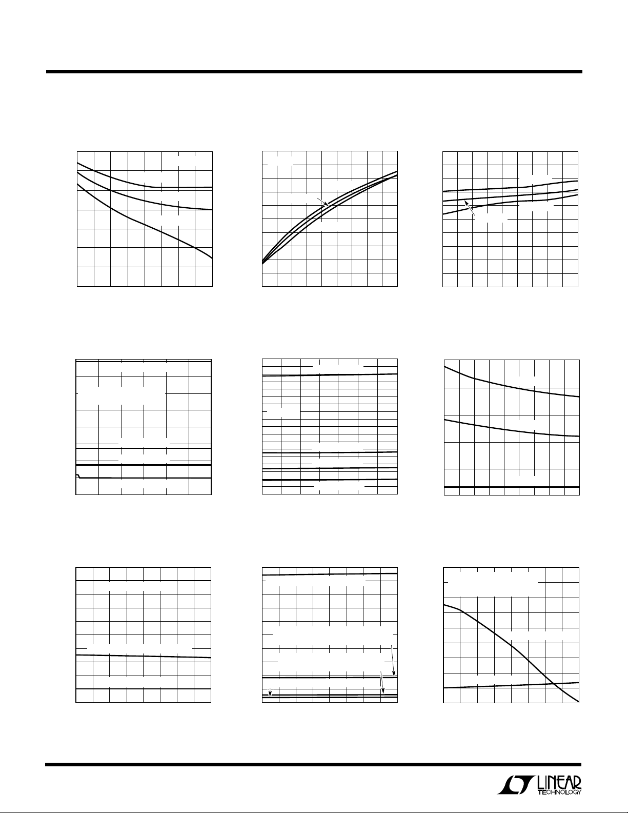
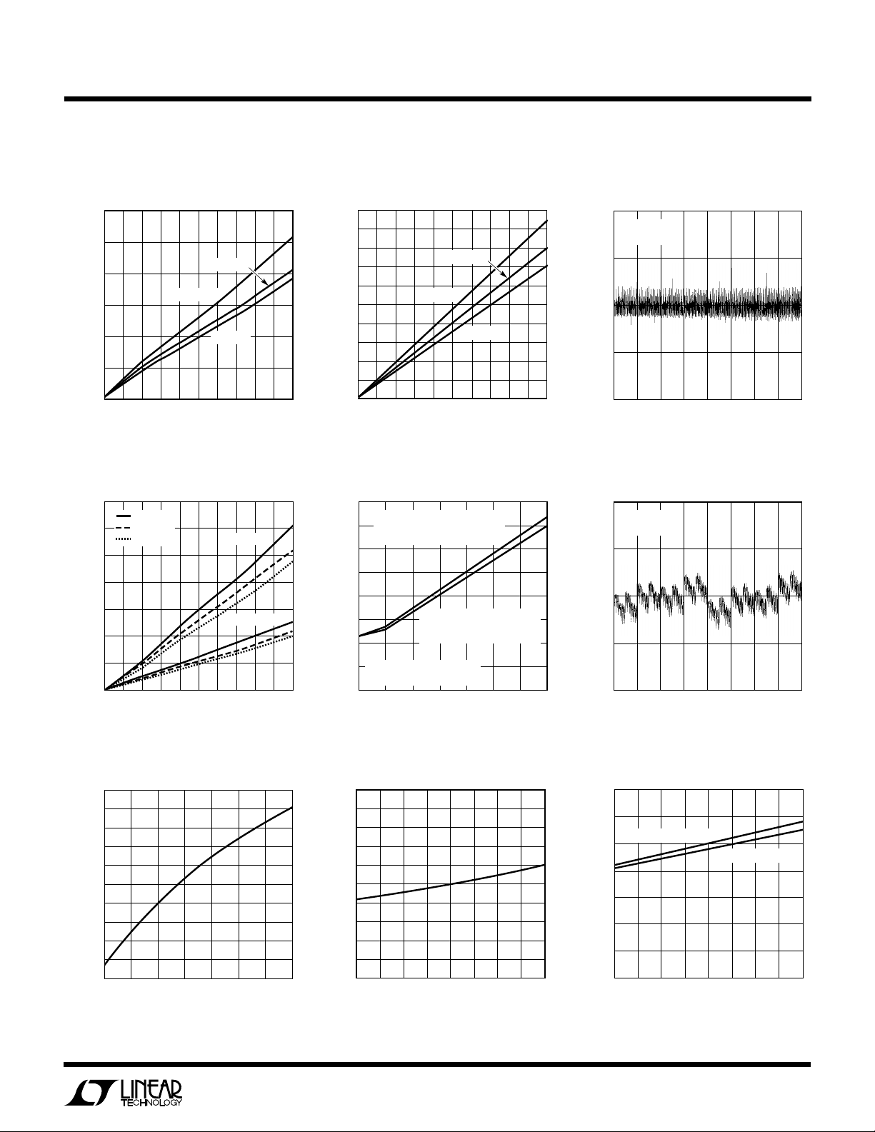
TYPICAL PERFORMANCE CHARACTERISTICS
Regulator Output Voltage vs
Load Current
3.077
3.076
3.075
3.074
3.073
3.072
3.071
REGULATOR OUTPUT VOLTAGE (V)
3.070
0.5 1.0 1.5 2.5 3.52.0 4.0
0
VDD = 16V
VDD = 12V
VDD = 4.5V
LOAD CURRENT (mA)
Charge Current vs Battery Voltage
160
140
VDD = 12V, R
120
L = 100µH, P1: IRF9531
100
80
60
CHARGE CURRENT (mA)
40
20
0
0
VR1 = 1, VR0 = 1
= 1Ω,
SENSE
VR1 = 1, VR0 = 0
VR1 = 0, VR0 = 1
VR1 = 0, VR0 = 0
468
2
BATTERY VOLTAGE (V)
TA = 27°C
3.0
10 12
1325 G01
1325 G04
Regulator Output Voltage vs
Temperature
3.082
I
3.081
3.080
3.079
3.078
3.077
3.076
3.075
3.074
REGULATOR OUTPUT VOLTAGE (V)
3.073
3.072
= 0
REG
VDD = 16V
VDD = 12V
VDD = 4.5V
10 30
20
0
DAC Output Voltage vs
40
TEMPERATURE (°C)
70
50 90
60
80
1325 G02
Temperature
180
160
140
120
VDD = 12V
100
80
60
40
DAC OUTPUT VOLTAGE (mV)
20
0
0
10 20
VR1 = 1, VR0 = 1
VR1 = 1, VR0 = 0
VR1 = 0, VR0 = 1
VR1 = 0, VR0 = 0
40 60 70
30 50
TEMPERATURE (°C)
1325 G05
VDD Supply Current vs
Temperature
Shutdown Current vs Temperature
Fault Comparator Threshold vs
Temperature
1.0
0.9
0.8
0.7
0.6
0.5
0.4
0.3
0.2
0.1
FAULT COMPARATOR THRESHOLD (V)
0
4
V
CELL
V
FOR HTF = HIGH, V
TBAT
V
CELL
0
10 30
20
FOR EDV = HIGH
FOR BATR = HIGH
TEMPERATURE (°C)
Fault Comparator Threshold vs
Temperature
11
10
V
FOR BATP = HIGH, VDD = 12V
BAT
9
8
7
V
6
= 0.4V
HTF
70
60
50
80
1325 G07
40
5
4
3
FAULT COMPARATOR THRESHOLD (V)
2
1
0
V
V
FOR MCV = HIGH, V
CELL
V
TBAT
V
FOR HTF = HIGH, V
TBAT
10 30
20
FOR LTF = HIGH, V
TBAT
FOR LTF = HIGH, V
40
TEMPERATURE (°C)
FOR MCV = HIGH, V
CELL
HTF
50
= 2.8V AND
MCV
MCV
LTF
= 1.35V
60
= 2.8V
LTF
= 1.6V
= 1.6V
70
80
1325 G08
Gas Gauge Gain and Offset vs
Temperature
0
V
= –0.2V AND –0.4V
SENSE
–0.5
INCLUDES CHANGES IN V
WITH TEMPERATURE
–1.0
–1.5
–2.0
–2.5
–3.0
–3.5
–4.0
GAS GAUGE GAIN AND OFFSET (COUNTS)
–4.5
GAS GAUGE GAIN
10 20 30 40 50 80
0
TEMPERATURE (°C)
REG
GAS GAUGE OFFSET
7060
1325 G09
UW
TEMPERATURE (°C)
0
CLK TO D
OUT
VALID DELAY TIME (ns)
400
500
600
60
1325 G18
300
200
10 20 30 50 7040
80
100
0
700
D
OUT
GOING HIGH
D
OUT
GOING LOW
TYPICAL PERFORMANCE CHARACTERISTICS
LTC1325
PGATE Rise Time vs
Load Capacitance
1200
1000
800
600
400
PGATE RISE TIME (ns)
200
0
Discharge Rise and Fall Time
vs Load Capacitance
14
12
10
8
6
4
2
DISCHARGE RISE AND FALL TIME (µs)
0
0
Oscillator Frequency vs
Temperature
118
117
116
115
114
113
112
111
110
OSCILLATOR FREQUENCY (kHz)
109
108
–40
TA = 27°C
TA = 70°C
4 8 12 16
LOAD CAPACITANCE (nF)
TA = 70°C
= 27°C
T
A
= 0°C
T
A
6
10
8
4
2
LOAD CAPACITANCE (nF)
40
20
0
–20
TEMPERATURE (°C)
TA = 0°C
RISE TIME
FALL TIME
14
12 16
60
80
1325 G10
18
1325 G13
1325 G16
2020 6 10 14 18
20
100
PGATE Fall Time vs
Load Capacitance
1000
900
800
700
600
500
400
300
PGATE FALL TIME (ns)
200
100
0
42 6 10 14 18
0
LOAD CAPACITANCE (nF)
TA = 27°C
TA = 70°C
8
Minimum Charging Supply vs
Number of Cells
16
14
12
10
8
6
4
MINIMUM CHARGE VOLTAGE (V)
2
0
1
CLK to D
= 0.15, VR1 = 1,VR0 = 1
R
SENSE
L = 10µH TO 100µH
IRF9Z30PFET, 1N5819 DIODE
R
= 1, VR1 = 1, VR0 = 1
SENSE
L = 25µH TO 100µH
IRF9Z30PFET, 1N5819 DIODE
TA = 27°C, NiCd BATTERIES
= 1.4V NOMINAL
V
CELL
35
2468
NUMBER OF CELLS
Enable Delay Time
OUT
vs Temperature
500
450
400
350
300
250
200
ENABLE DELAY TIME (ns)
150
OUT
100
50
CLK TO D
0
0
10 30
20
40
TEMPERATURE (°C)
TA = 0°C
12
50
Differential Nonlinearity
1.0
VDD = 12V
= 500kHz
f
CLK
0.5
0
–0.5
DIFFERENTIAL NONLINEARITY (LSB)
16
20
LTC1325 G11
–1.0
128 384 640
0
256
512
CODE
768
896
1024
1325 G12
Integral Nonlinearity
1.0
VDD = 12V
= 500kHz
f
CLK
0.5
0
–0.5
INTEGRAL NONLINEARITY (LSB)
7
1325 G14
–1.0
128 384 640
0
CLK to D
256
512
CODE
Valid Delay Time
OUT
768
896
1024
1325 G15
vs Temperature
70
60
80
1325 G17
5

LTC1325
PIN FUNCTIONS
UUU
REG (Pin 1): Internal Regulator Output. The regulator
provides a steady 3.072V to the internal analog circuitry
and provides a temperature stable reference voltage for
generating MCV, HTF, LTF and thermistor bias voltages
with external resistors. Requires a 4.7µ F or greater bypass
capacitor to ground.
D
(Pin 2): TTL Data Output Signal for the Serial
OUT
Interface. D
3-wire interface, or remain separated to form a 4-wire
interface. Data is transmitted on the falling edge of CLK
(Pin 5).
DIN (Pin 3): TTL Data Input Signal for the Serial Interface.
The data is latched into the chip on the rising edge of the
CLK (Pin 5).
CS (Pin 4): TTL Chip Select Signal for the Serial Interface.
CLK (Pin 5): TTL Clock for the Serial Interface.
LTF (Pin 6): Minimum Allowable Battery Temperature
Analog Input. LTF may be generated by a resistive divider
between REG (Pin 1) and ground.
MCV (Pin 7): Maximum Allowable Cell Voltage Analog
Input. MCV may be generated by a resistive divider between REG (Pin 1) and ground.
HTF (Pin 8): Maximum Allowable Battery Temperature
Analog Input. HTF may be generated by a resistive divider
between REG (Pin 1) and ground.
GND (Pin 9): Ground.
FILTER (Pin 10): The external filter capacitor CF is con-
nected to this pin. The filter capacitor is connected to the
output of the internal resistive divider across the battery to
reduce the switching noise while charging. In the gas
gauge mode, CF along with an internal RF = 1k form a
lowpass filter to average the voltage across the sense
resistor.
and DIN may be tied together to form a
OUT
SENSE (Pin 11): The Sense pin controls the switching of
the 111kHz PWM constant current source in the charging
mode. The Sense pin is connected to an external sense
resistor R
charging loop forces the average voltage at the Sense pin
to equal a programmable internal reference voltage V
The battery charging current is equal to V
In the gas gauge mode the voltage across the Sense pin
is filtered by an RC network (RF and CF), amplified by
an inverting gain of four, then multiplexed to the ADC so
the average discharge current through the battery may
be measured and the total charge leaving the battery
calculated.
VIN (Pin 12): General Purpose ADC Input.
T
(Pin 13): Ambient Temperature Input. Connect to an
AMB
external thermistor network. Tie to REG if not used. May
be used as another general purpose ADC input.
T
(Pin 14): Battery Temperature Input. Connect to an
BAT
external NTC thermistor network. Tie to REG if not used.
V
(Pin 15): Battery Input. An internal voltage divider is
BAT
connected between the V
all battery measurements to one cell voltage. The divider
is programmable to the following ratios: 1/1, 1/2, 1/3 . . .
1/15, 1/16. In shutdown and gas gauge modes the divider
is disconnected.
DIS (Pin 16): Active High Discharge Control Pin. Used
to turn on an external transistor which discharges the
battery.
PGATE (Pin 17): FET Driver Output. Swings from GND
to VDD.
VDD (Pin 18): Positive Supply Voltage. 4.5V < VDD < 16V.
and the negative side of the battery. The
SENSE
DAC/RSENSE
and Sense pins to normalize
BAT
DAC
.
.
6
BLOCK DIAGRAM
18
V
DD
5V
DIGITAL
REGULATOR
9
GND
5
CLK
4
CS
D
IN
D
OUT
SERIAL
3
2
A/D CONVERTER
I/O
10
10-BIT
2
W
DIGITAL INPUT CIRCUITS
CONTROL
LOGIC
PS, MSBF
DS0 TO DS1
3
SGL/DIFF
ADC
MUX
BATP, BATR, FMCV,
FEDV, FHTF, FLTF, t
7
MOD0 TO MOD1, PS
3
LTC1325
PS
OUT
3.072V
ANALOG
REGULATOR
FAULT
DETECT
CIRCUITRY
ANALOG AND DIGITAL V
DIV0 TO DIV3
4
ADC REFERENCE
t
OUT
DD
1
REG
16
DIS
6
LTF
8
HTF
7
MCV
12
V
IN
13
T
AMB
14
T
BAT
15
V
BAT
DIVIDER
TIMEOUT LOGIC
TEST CIRCUITS
Load Circuit for t
D
OUT
T
OUT
TO0 TO TO2
dDO
3
, tr and t
1.4V
3k
100pF
LTC1325 • TC01
GAS GAUGE
111kHz
OSCILLATOR
DR0 TO DR3
DUTY RATIO
GENERATOR
f
5 MOD0 TO MOD1, VR0 TO VR1, PS
PS
CHARGE LOOP
AND
GAS GAUGE
3
LTC1325 • BD
Load Circuit for t
TEST POINT
D
OUT
3k
100pF
CHARGE
dis
and t
11
SENSE
10
FILTER
17
PGATE
en
5V t
WAVEFORM 2, t
dis
t
WAVEFORM 1
dis
LTC1325 • TC02
en
7
LTC1325
0.4V
2.4V
t
r
t
f
LTC1325 • TC04
TEST CIRCUITS
Voltage Waveforms for D
D
CLK
OUT
0.8V
t
dDO
On and Off Channel Leakage Voltage Waveforms for t
3.072V
NOTE: EXTERNAL CHANNELS ONLY––
, T
BAT
AMB
AND V
IN
T
Delay Time, t
OUT
dDO
2.4V
0.4V
LTC1325 • TC03
Voltage Waveforms for D
Rise and Fall Times, tr, t
OUT
f
dis
I
ON
A
I
OFF
A
ON CHANNEL
OFF
}
CHANNELS
LTC1325 • TC05
WAVEFORM 1
(SEE NOTE 1)
WAVEFORM 2
(SEE NOTE 2)
NOTE 1: WAVEFORM 1 IS FOR AN OUTPUT WITH INTERNAL CONDITIONS
SUCH THAT THE OUTPUT IS HIGH UNLESS DISABLED BY CS.
NOTE 2: WAVEFORM 2 IS FOR AN OUTPUT WITH INTERNAL CONDITIONS
SUCH THAT THE OUTPUT IS LOW UNLESS DISABLED BY CS.
CS
D
OUT
t
dis
D
OUT
2V
90%
10%
LTC1325 • TC06
Voltage Waveforms for t
CS
D
IN
CLK
D
OUT
START
121222324
en
VR1
0.4V
t
en
THREE-STATE NULL
0.4V
D9
LTC1325 • TC07
8

UW W
TI I G DIAGRA
MSB-FIRST DATA (MSBF = 1)
CS
CLK
START
D
IN
D
OUT
MSB-FIRST DATA (MSBF = 0)
CS
CLK
START
D
IN
HI-Z
D
OUT
NOTE: THE TIMING DIAGRAM SHOWS TWO POSSIBLE COMMAND WORDS.
REFER TO FUNCTIONAL DESCRIPTION FOR INFORMATION ON HOW TO
CONSTRUCT THE COMMAND WORD
MSBF
COMMAND WORD
COMMAND WORD
VR1
NULL
ADC DATA STATUS WORD
NULL
D9 D9
D1 D1
D0
ADC DATA STATUS WORD
D1D9 D0
LTC1325
FSBATP
FSBATP
HI-ZHI-Z
HI-Z
LTC1325 • TD
UU
U
FUNCTIONAL DESCRIPTIO
GENERAL DESCRIPTION
During normal operation, a command word is shifted into
the chip via the serial interface, then an ADC measurement
is made and the 10-bit reading and chip status word are
shifted out. The command word configures the LTC1325
and forces it into one of five modes: power shutdown, idle,
discharge, charge or gas gauge mode.
In the power shutdown mode, the analog section is turned
off and the supply current drops to 30µA. The voltage
regulator, which provides power to the internal analog
circuitry and external bias networks, is shut down. The
voltage divider across the battery is disconnected and only
the voltage regulator for the serial interface logic is left on.
During the idle mode, the chip is fully powered but the
discharge, charge, and gas gauge circuits are off. The chip
may be placed in the idle mode momentarily while charging the battery, allowing an ADC measurement to be made
without any switching noise from the PWM current source
affecting the accuracy of the reading. The mode command
bits are picked off as they appear at DIN, allowing the
charging loop to turn off and settle while the remainder of
the command word is being shifted in.
During the discharge mode, the battery is discharged by
an external transistor and series resistor. The battery is
monitored for fault conditions.
In the charge mode, the µ P monitors the battery’s voltage,
temperature and ambient temperature via the 10-bit ADC.
Termination methods such as –∆V
∆T
BAT
, ∆T
/∆Time, ∆(T
BAT
– TA), maximum tempera-
BAT
BAT
, ∆V
BAT
/∆Time,
ture, maximum voltage and maximum charge time may be
accurately implemented in software. The LTC1325 also
monitors the battery for fault conditions.
In the gas gauge mode, the average voltage across the
sense resistor can be measured to determine the average
battery load current. The sense voltage is filtered by an RC
circuit, multiplied by an inverting gain of four, then converted by the ADC. The µP can then accumulate the ADC
measurements and do a time average to determine the
total charge leaving the battery. The RC circuit consists of
an internal 1k resistor RF and an external capacitor C
F
connected to the Filter pin.
9

LTC1325
UU
U
FUNCTIONAL DESCRIPTIO
COMMAND WORD
The command word is 22 bits long and contains all the
information needed to configure and control the chip. On
power-up all bits are cleared to logical “0.”
1
START
MOD02MOD1
= 1
DIV09DIV110DIV2
FSCLR17TO018TO1
3
4
SGL/
MSBF5DS06DS17DS2
DIFF
12
11
PS13DR014DR115DR2
DIV3
20
19
TO2
22
VR021VR1
LTC1325 • F01
Figure 1. Command Word
Bit 1: Start Bit (Start)
The first “logical one” clocked into the DIN input after CS
goes low is the start bit. The start bit initiates the data
transfer and all leading zeros which precede this logical
one will be ignored. After the start bit is received, the
remaining bits of the command word will be clocked in.
Bits 2 and 3: Mode Select (MOD0 and MOD1)
8
16
Bit 5: MSB-First/LSB-First (MSBF)
The ADC data is programmed for MSB-first or LSB-first
sequence using the MSBF bit. See Serial I/O description
for details.
MSBF DESCRIPTION
0 LSB-First Data Follows MSB-First Data
1 MSB-First Data Only
Bits 6 to 8: ADC Data Input Select (DS0 to DS2)
DS2, DS1 and DS0 select which circuit is connected to the
ADC input. Do not use unlisted combinations.
DS2 DS1 DS0 DESCRIPTION
0 0 0 Gas Gauge Output
0 0 1 Battery Temperature Pin, T
0 1 0 Ambient Temperature Pin, T
0 1 1 Battery Divider Output Voltage, V
100V
Pin
IN
BAT
AMB
CELL
Bits 9 to 12: Battery Divider Ratio Select (DIV0 to DIV3)
DIV3, DIV2, DIV1 and DIV0 select the division ratio for the
voltage divider across the battery.
The two mode bits determine which of four modes the chip
will be in: idle, discharge, charge or gas gauge.
MOD1 MOD0 DESCRIPTION
0 0 Idle
0 1 Discharge
1 0 Charge
1 1 Gas Gauge
Bit 4: Single-Ended Differential Conversion (SGL/DIFF)
SGL/DIFF determines whether the ADC makes a singleended measurement with respect to ground or a differential measurement with respect to the Sense pin.
SGL/DIFF DESCRIPTION
0 Single-Ended ADC Conversion
1 Differential ADC Conversion (with respect to Sense)
DIV3 DIV2 DIV1 DIV0 DESCRIPTION
0000(V
0001(V
0010(V
0011(V
0100(V
0101(V
0110(V
0111(V
1000(V
1001(V
1010(V
1011(V
1100(V
1101(V
1110(V
1111(V
BAT
BAT
BAT
BAT
BAT
BAT
BAT
BAT
BAT
BAT
BAT
BAT
BAT
BAT
BAT
BAT
– V
– V
– V
– V
– V
– V
– V
– V
– V
– V
– V
– V
– V
– V
– V
– V
SENSE
SENSE
SENSE
SENSE
SENSE
SENSE
SENSE
SENSE
SENSE
SENSE
SENSE
SENSE
SENSE
SENSE
SENSE
SENSE
)/1
)/2
)/3
)/4
)/5
)/6
)/7
)/8
)/9
)/10
)/11
)/12
)/13
)/14
)/15
)/16
10

LTC1325
UU
U
FUNCTIONAL DESCRIPTIO
Bit 13: Power Shutdown (PS)
PS selects between the normal operating mode, or the
shutdown mode.
PS DESCRIPTION
0 Normal Operation
1 Shutdown All Circuits Except Digital Inputs
Bits 14 to 16: Duty Ratio Select (DR0 to DR2)
DR2, DR1 and DR0 select the duty cycle of the charging
loop operation (not 111kHz PWM duty cycle). The last
three selections place the chip into a test mode and should
not be used.
DR2 DR1 DR0 DESCRIPTION
0 0 0 1/16
0 0 1 1/8
0 1 0 1/4
0 1 1 1/2
1001
1 0 1 Test Mode 1
1 1 0 Test Mode 2
1 1 1 Test Mode 3
Bits 21 and 22: Charging Loop Reference Voltage
Select (VR0 and VR1)
VR1 and VR0 select the desired reference voltage V
CHRG
for the charging loop. The charging loop will force the
average voltage at the Sense pin to be equal to V
average charging current is V
VR1 VR0 V
0018
0134
1055
1 1 160
DAC
(mV)
DAC/RSENSE
(see Figure 4).
DAC
. The
STATUS WORD
The status word is 8 bits long and contains the status of
the internal fail-safe circuits.
3
BATP1BATR2FMCV
Figure 2. Status Word
4
FEDV
FHTF5FLTF6t
7
OUT
8
FS
LTC1325 • F02
Bit 17: Fail-Safe Latch Clear (FSCLR)
When FSCLR bit is set to one, the internal fail-safe timer is
reset to 0, and the fail-safe latches are reset. FSCLR is
automatically reset to 0 when CS goes high.
FSCLR DESCRIPTION
0 No Action
1 Reset Fail-Safe Timer and Latches
Bits 18 to 20: Timeout Period Select (TO0 to TO2)
TO2, TO1 and TO0 select the desired fail-safe timeout
period,t
TO2 TO1 TO0 TIMEOUT (MINUTES)
0005
00110
01020
01140
10080
1 0 1 160
1 1 0 320
1 1 1 Indefinite (No Timeout)
. On power-up, the default timeout is 5 minutes.
OUT
Bit 1: Battery Present (BATP)
The BATP bit = 1 indicates the presence of the battery. The
bit is set to 1 when the voltage at the V
pin falls below
BAT
(VDD – 1.8V). BATP = 0 when the battery is removed and
V
is pulled high by R
BAT
BATP CONDITIONS
0(V
1V
– 1.8) < V
DD
< (VDD – 1.8)
BAT
(see Figure 3).
TRK
< V
BAT
DD
Bit 2: Battery Reversed (BATR) or Shorted
The BATR bit indicates when the battery is connected
backwards or shorted. The bit is set when the battery cell
voltage at the output of the battery divider V
CELL
is below
100mV.
BATR CONDITIONS
0V
1V
CELL
CELL
> 100mV
< 100mV
11

LTC1325
+
–
+
–
+
–
V
DD
BATP
FMCV
PROGRAMMABLE
BATTERY
DIVIDER
C2
C1
1.8V
C3
C4
+
–
FEDV
+
–
BATR
V
DD
V
BAT
SENSE
MCV
900mV
100mV
T
BAT
HTF
R4
R3 R
L
R
T
LTC1325 • F03
LTF
REG
REG
R
TRK
R1
R2
3.072V
LINEAR
REGULATOR
C5
+
–
FHTF
C6
+
–
FLTF
UU
U
FUNCTIONAL DESCRIPTIO
Bit 3: Maximum Cell Voltage (FMCV)
The MCV bit indicates when the battery cell voltage has
exceeded the preset limit. The bit is set when V
greater than the voltage at the MCV pin.
FMCV CONDITIONS
0V
1V
CELL
CELL
< V
> V
MCV
MCV
Bit 4: End Discharge Voltage (FEDV)
The EDV bit indicates when the battery cell voltage has
dropped below an internally preset limit. The bit is set
when the battery cell voltage at the output of the voltage
divider V
FEDV CONDITIONS
0V
1V
is less than 900mV.
CELL
> 900mV
CELL
< 900mV
CELL
Bit 5: High Temperature Fault (FHTF)
The HTF bit indicates when the battery temperature is too
high. Using a negative TC thermistor, the bit is set when
the voltage at the T
pin is less than the voltage at the
BAT
HTF pin.
CELL
is
T
OUT
0 No Timeout Has Occurred
1 Timeout Has Occurred
CONDITIONS
Bit 8: Fail-Safe Occurred (FS)
The FS bit indicates that one of the fault detection circuits
halted the discharging or charging cycle. The bit is set
when an EDV, LTF, HTF, or t
fault occurs during
OUT
discharge. During charging, the bit is set when a MCV,
LTF, HTF, or t
fault occurs. The bit is reset by the
OUT
command word bit FSCLR.
FS CONDITIONS
0 No Fail-Safe Has Occurred
1 Fail-Safe Has Occurred
DETAILED DESCRIPTION
Fault Conditions
The LTC1325 monitors the battery for fault conditions
before and during discharge and charge (see Figure 3).
They include: battery removed/present (BATP), battery
reversed/shorted (BATR), maximum cell voltage exceeded
FHTF CONDITIONS
0T
1T
BAT
BAT
> V
< V
HTF
HTF
Bit 6: Low Temperature Fault (FLTF)
The LTF bit indicates when the battery temperature is too
low. Using a negative TC thermistor, the bit is set when the
voltage at the T
LTF pin.
Bit 7: Timeout (t
The t
exceeded the preset limit. The bit is set when the internal
timer exceeds the limit set by the command bits TO0, TO1
FLTF CONDITIONS
0T
1T
BAT
BAT
BAT
< V
> V
OUT
bit indicates that the battery charging time has
OUT
pin is greater than the voltage at the
LTF
LTF
)
and TO2.
12
Figure 3. Fail-Safe or Fault Detection Circuitry

LTC1325
UU
U
FUNCTIONAL DESCRIPTIO
(MCV), minimum cell voltage exceeded (EDV), high temperature limit exceeded (HTF), low temperature limit exceeded (LTF) and time limit exceeded (t
condition occurs, the discharge and charge loops are
disabled or prevented from turning on and the fail-safe bit
(FS) is set. The chip is reset by shifting in a new command
word with the fail-safe clear FSCLR bit set. The 8-bit status
word contains the state of each fault condition.
Power Shutdown Mode
Command: MOD1 = X, MOD0 = X, PS = 1
Status: BATP = X, BATR = X, FMCV = X, FEDV = X,
FHTF = X, FLTF = X, t
In the power shutdown mode, the analog section is turned
off and the supply current drops to 30µA. The voltage
regulator, which provides power to the internal analog
circuitry and external bias networks, is shut down. The
voltage divider across the battery is disconnected and the
only circuit left on is the voltage regulator for the serial
interface logic.
OUT
). When a fault
OUT
= X
The chip enters the discharge mode when the proper
mode command bits are set and the power shutdown
command bit is clear. If a fault condition does not exist,
then the DIS pin is pulled up to VDD by the internal driver.
The DIS voltage is used to turn on an external transistor
which discharges the battery through an external series
resistor R
Discharging will continue until a new command word is
input to change the mode or a fault condition occurs.
Charge Mode
Command: MOD1 = 1, MOD0 = 0, PS = 0
Status: BATP = 1, BATR = 0, FMCV = 0, FEDV = X,
The chip enters the charge mode when the proper mode
command bits are set and the power shutdown command
bit is clear. If a fault condition does not exist then charging
can begin. Charging will continue until a new command
word is input to change the mode or a fault condition
occurs.
.
DIS
FHTF = 0, FLTF = 0, t
OUT
= 0
Idle Mode
Command: MOD1 = 0, MOD0 = 0, PS = 0
Status: BATP = X, BATR = X, FMCV = X, FEDV = X,
FHTF = X, FLTF = X, t
The chip enters the idle mode when the proper mode
command bits are set and the power shutdown command
bit is cleared. During the idle mode, the chip is fully
powered, but the discharge, charge and gas gauge circuits
are off. The chip may be placed in the idle mode momentarily while charging the battery, allowing an ADC measurement to be made without any switching noise from the
PWM current source affecting the accuracy of the reading.
The mode command bits are picked off as they appear at
DIN, so that while the rest of the command word is being
shifted in, the charging loop has time to settle before an
ADC measurement is made.
Discharge Mode
Command: MOD1 = 0, MOD0 = 1, PS = 0
Status: BATP = 1, BATR = 0, FMCV = X, FEDV = 0,
FHTF = 0, FLTF = 0, t
OUT
OUT
= X
= 0
The charge current may be regulated by a programmable
111kHz PWM buck current regulator, or by using the PFET
to gate an external current regulator or current limited
transformer.
111kHz PWM Controller
The block diagram of the charging loop connected as a
PWM buck current regulator is shown in Figure 4. The
PWM may operate in either continuous or discontinuous
mode. The loop forces the average voltage across the
sense resistor to be equal to the voltage at the output of the
DAC, so that the charging current becomes V
With switch S2 on and the others off, amplifier A1 along
with C1, R1 and R2 are configured as an integrator with
16kHz bandwidth. The output of the integrator is the
average difference between the voltage across the sense
resistor and the DAC output voltage.
The rising edge of the oscillator waveform triggers the one
shot which sets the flip-flop output high. This turns on the
external PFET P1 by pulling its gate low via the FET driver.
With P1 on, the current through the inductor L1 starts to
DAC/RSENSE
.
13

LTC1325
UU
FUNCTIONAL DESCRIPTIO
CHARGE
3
DR0 TO
DR2
111kHz
OSCILLATOR
TO
ADC MUX
SQ
R
GG
0
0
0
0
1
DUTY RATIO
GENERATOR
ONE SHOT
VR1
VR0
0
0
0
1
1
0
1
1
X
X
+
A2
–
DAC VOLTAGE
18mV
34mV
55mV
160mV
0mV
U
GG
C1
16pF
A1
S1
–
+
V
DAC
DISCHARGE
R2
R1
125k
500k
S2
S3
REG
3.072V
DAC
2
VR0, VR1 GG
R
F
1k
S4
(GAS GAUGE)
PGATE
DIS
SENSE
FILTER
CHIP
BOUNDARY
BATTERY
VDD
4.5V TO 16V
P1
IRF9Z30
L1
C
F
R
SENSE
D1
1N5818
IRFZ34
N1
LTC1325 • F04
R
TRK
R
DIS
Figure 4. Charging Loop Block Diagram
rise as does the voltage across the sense resistor. When
the voltage across the sense resistor is greater than the
output of the integrator, comparator A2 changes state.
This resets the flip-flop and P1 is turned off. Catch diode
D1 clamps the drain of P1 one diode drop below ground
when the inductor flies back and the current through the
inductor starts to drop. The voltage across the sense
resistor also drops and may reach zero and stay there until
the next clock cycle begins.
The average charging current is set by the output of the
DAC (V
) and the duty ratio generator. V
DAC
DAC
can be
programmed to one of four values with the following
ratios: 1, 1/3, 1/5 or 1/10. The duty ratio can be set to
1/16, 1/8, 1/4, 1/2 or 1. When the duty ratio is 1, the duty
ratio generator output is always low and the charge loop
operates continuously (see Figure 4). At other duty ratio
settings, the duty generator output is a square wave with
a period of 42 seconds. The time for which the generator
output is low varies with the duty ratio setting. For ex-
ample, if a duty ratio of 1/2 is programmed, the generator
output is low only for 42/2 = 21 seconds. Since the loop
operates for only 21 out of every 42 seconds, the average
charging current is halved. In general, the average charging current is:
I
CHRG
= V
(Duty Ratio)/R
DAC
SENSE
Gated PFET Controller
When using an external current regulator or current limited wall pack, simply remove the inductor L1 and catch
diode D1. Set the DAC control bits VR1 = 1 and VR0 = 1,
and select the desired duty ratio. By insuring that the
voltage at the Sense pin is never greater than 140mV, the
output of the integrator A1 will saturate high and the
comparator A2 will never trip and turn the loop off. This
can be achieved by removing the sense resistor and
grounding the Sense pin or if the gas gauge is to be used,
selecting R
SENSE
so that R
SENSE/ICHRG
< 140mV.
14

LTC1325
UU
U
FUNCTIONAL DESCRIPTIO
Gas Gauge Mode
Command: MOD1 = 1, MOD0 = 1, PS = 0
Status: BATP = X, BATR = X, FMCV = X, FEDV = X,
FHTF = X, FLTF = X, t
In the gas gauge mode, the average voltage across the
sense resistor can be measured to determine the average
battery load current. The output of the DAC is set to ground
and switches S1, S3 and S4 are closed. A1 is configured
as an inverting amplifier with R1 and R2 setting the gain
to –4. The voltage across the sense resistor is filtered by
an RC circuit (RF, CF) amplified by A1, then converted by
the ADC.
The microprocessor can then accumulate the ADC measurements and do a time average to determine the total
charge leaving the battery. The Sense pin voltage should
not be more negative than –450mV to ensure linearity.
The RFCF circuit consists of an internal 1k resistor and an
external capacitor connected to the Filter pin. RFCF should
be longer than the measurement interval. With the serial
clock running at 100kHz, it take 380µs to shift in the
command word and shift out the ADC measurement and
status word.
Trickle Resistor
An external trickle resistor has several functions. First, it
provides a continuous trickle charge current for topping
off the battery and countering the effects of self-discharge.
Second, it can be used to condition a deeply discharged
battery for charging. The LTC1325 will not charge a battery
unless its cell voltage is above 100mV (BATR). Finally, the
resistor is required by the battery detect circuit to pull the
V
pin high when the battery is removed.
BAT
SERIAL INTERFACE
The LTC1325 communicates with microprocessors and
other external circuitry via a synchronous, half duplex,
4-wire serial interface. The clock CLK synchronizes the
data transfer with each bit being transmitted on the falling
edge and captured on the rising CLK edge in both transmitting and receiving systems. The LTC1325 first receives
input data and then transmits back the A/D conversion
result and status word (half duplex). Because of the half
OUT
= X
duplex operation, DIN and D
allowing transmission over just three wires: CS, CLK and
DATA (DIN/D
Data transfer is initiated by a falling chip select CS signal.
After CS falls, the LTC1325 looks for a start bit on DIN. The
start bit is the first “logical one” clocked into the DIN input
after CS goes low. The LTC1325 will ignore all leading
zeros which precede this logical one. After the start bit is
received, the 21 other control bits are shifted into the D
pin to configure the LTC1325 and start a conversion. After
the last command bit, the D
for one clock period before it is taken low for one null bit.
Following the null bit, the conversion results and the 8
status bits are shifted out on the D
data exchange, CS should be brought high.
MSB-First/LSB-First (MSBF Control Bit)
The output data of the LTC1325 is programmed for MSBfirst or LSB-first sequence using the MSFB control bit.
When MSBF = 1, data will appear on D
format. This is followed by the 8 status bits. Logical zeros
will be filled in indefinitely following the last data bit to
accommodate longer word lengths required by some
microprocessors. When MSBF = 0, LSB-first data will
follow the MSB-first data. Regardless of the state of
MSBF, the status bits are always shifted out in the same
order (see Figure 2).
Accommodating Microprocessors with Different Word
Lengths
The LTC1325 will fill zeros indefinitely after the transmitted data until CS is brought high. At that time D
disabled (three-stated). This makes for easy interfacing
to MPU serial ports with different transfer increments
including 4 bits (e.g., COP400) and 8 bits (e.g., SPI and
MICROWIRE/PLUSTM). Any word length can be accommodated by the correct positioning of the start bit in the
input word.
Operation with DIN and D
The LTC1325 can be operated with DIN and D
together. This eliminates one of the lines required to
MICROWIRE/PLUS is a trademark of National Semiconductor Corp.
OUT
).
OUT
may be tied together
OUT
pin remains in three-state
OUT
pin. At the end of the
OUT
in MSB-first
OUT
Tied Together
OUT
OUT
tied
IN
is
15

LTC1325
β=
−
T
T
TT
In
R
R
O
O
T
TO
dV
dT
VT
T
T
DIV
DIV O
O
O
=
()
−
+
–
β21
2
UU
U
FUNCTIONAL DESCRIPTIO
communicate with the microprocessor. Data is transmitted in both directions on a single wire. The processor pin
connected to this data line should be configurable as either
an input or an output. The LTC1325 will take control of the
data line and drive it low after the 23rd falling CLK edge
after the start bit is received. Therefore the processor port
must be switched to an input before this happens to avoid
a conflict.
Power-Up After Shutdown
When a control word with the PS bit set to one is written
to the LTC1325, it enters shutdown mode in which the V
supply current is reduced to 30µA. In this mode the on-
chip 3V regulator and all circuits powered off it are shut
down. The only circuits that remain alive are DIN, CS and
CLK input buffers. To take the LTC1325 out from shutdown mode, a high to low edge must be applied to the CS
pin. Either DIN or CLK must be low when CS is low to
prevent a false control word from being transmitted to the
LTC1325. The 3V output decays with a time constant of
300ms with C
= 4.7µF. The microprocessor should
REG
wait three seconds before applying a wake-up edge to the
CS pin to ensure proper power-up.
DD
exp β
−
β
+
β
T
dT
11
T
2
T
2
R
T
=−
RTT
TO O
RR
=
LTO
1RdR
α=
T
−
αβ=
2
T
O
O
where,
V
(T) is the output of the divider,
DIV
(2)
(3)
(4)
(5)
(6)
(7)
TEMPERATURE SENSING
NTC (Negative Temperature Coefficient) Thermistors
The simplest method to sense temperature (battery or
ambient) with an NTC thermistor is to use a voltage divider
powered by the REG pin. This divider consists of a load
resistor RL in series with a thermistor RT as shown in
Figure 3. For a given thermistor, there is a value of R
which makes V
(T) linear over a narrow but adequate
DIV
L
temperature range. The easiest method (Inflection Point
Method) to calculate RL is to set the second temperature
derivative of the divider output to 0. The equations relevant
to this method are:
VT
()
DIV
V
REG
=
1
+
R
1
R
L
T
=
fT
()
(1)
V
is the voltage at the REG pin (3.072V nominal),
REG
RT is the thermistor resistance at some temperature T,
RTO is the thermistor resistance at some reference
temperature TO,
β is a constant dependent on thermistor material,
α is the temperature coefficient (in %/°C) of RT at
TO, and
all temperatures are in °K (i.e., T°C + 273)
There are two assumptions in the derivation of the above
equations. β is assumed to be constant and the temperature coefficient of RL is small compared to that of the
thermistor.
Most thermistor data sheets specify RTO, β, RT/RTO ratios
for two temperatures, α, and tolerances for β and RTO.
Given β, and RTO, it is easy to calculate RL from equation
16

LTC1325
U
WUU
APPLICATIONS INFORMATION
(3). Alternatively, β may be calculated from the RT/R
ratio using equation (4) or from α, using equation (6).
As a numerical example, consider the Panasonic
ERT-D2FHL103S thermistor which has the following characteristics:
1. RT (25°C) = RTO = 10k
2. α = –4.6%/°C at TO = 25°C
3. Ratio R25/R50 = 2.9
Using equation (4) and R25/R50 = 2.9, β = (323 × 298)In
(2.9)/(298 – 323) = 4099k. Alternatively, using equation
(6) and α = –4.6%/°C, β = –(– 0.046)(298)2 = 4085k.
Both values of β are close to each other. Substituting
β = 4085k into equation (3) gives RL = 10k [4085 – (2 ×
298)]/[4085 + (2 × 298)] = 7.45k. The nearest 1% resistor
value is 7.5k. Figure 5 shows a plot of V
(T) measured
DIV
at various temperatures for this thermistor with a 7.5k RL.
4.5
4.0
3.5
3.0
2.5
2.0
1.5
1.0
0.5
DIVIDER OUTPUT VOLTAGE (V)
0
–0.5
–60
Figure 5. ERT-D2FHL103S Divider
ACTUAL
–20
–40
TEMPERATURE (°C)
IDEAL
20
0
40
60
LTC1325 • F05
80
There are two methods of calculating battery or ambient
temperature from ADC readings of the T
channels. The first method is to store the V
BAT
or T
DIV
curve as a lookup table. The second method is to use a
straight line approximation. The equation of this line may
be calculated from the slope dV
/dT at TO [see equation
DIV
(7)] and assuming that the line passes through the point
[TO, V
)] on the curve. For the ERT-D2FHL103S, the
DIV(TO
slope is minus 34mV/°C and the equation of the line is
TO
AMB
(T) vs T
T = [2.605 – V
(T)]/0.034. The straight line approxima-
DIV
tion is accurate to within 2°C over a temperature range of
5°C to 45°C, assuming 3% β and 10% RTO tolerances.
PTC (Positive Temperature Coefficient) Thermistors
Positive Temperature Coefficient (PTC) thermistors may
be used in battery chargers that do not require accurate
temperature measurements. The resistance vs temperature characteristics of PTC exhibits a sharp increase at a
selectable switch temperature TS. This sharp change is
exploited in chargers which use TCO (Temperature Cutoff)
or ∆TCO (Difference between battery and ambient temperature). With TCO termination, a voltage divider consisting of a PTC and a low temperature coefficient load resistor
is connected between REG and GND with the top end of the
PTC at REG. The PTC is mounted on the battery to sense
its temperature. The divider output is tied to T
BAT
. When
the switch temperature is reached, the PTC resistance
increases sharply causing T
to fall below HTF. This
BAT
causes an HTF fault and charging is terminated. To implement ∆TCO termination, the load resistor can, in principle,
be replaced by a matching PTC and the divider now
responds to differences between battery and ambient
temperature. With both TCO and ∆TCO terminations, the
position of the battery temperature PTC can be swapped
with the load resistor or ambient temperature PTC. In both
cases, an LTF fault terminates charge when the trip point
is reached. Note that in practice, matched PTCs are not
readily available and for ∆TCO termination, NTC thermistors are recommended.
HARDWARE DESIGN PROCEDURE
This section discusses the considerations in selecting
each component of a simple battery charger (see Figures
3 and 4). Further applications assistance is provided in
Application Note 64, using the LTC1325 Battery Management IC.
1. R
a. LTC1325 V
: There are three factors in selecting R
SENSE
and Duty Ratio Settings
REF
SENSE
:
b. Sense Resistor Dissipation
c. I
LOAD(RSENSE
) < –450mV for Gas Gauge Linearity
17

LTC1325
U
WUU
APPLICATIONS INFORMATION
The LTC1325 has five duty ratio and four V
giving 20 possible charge rates (for a given value of
R
combination of V
) as shown in the following table. For any
SENSE
and duty ratio, the average
DAC
charging current is given by:
AVG I
NORMALIZED
V
DAC
1(VR1 = 1, VR0 = 1) 1 1/2 1/4 1/8 1/16
1/3(VR1 = 1, VR0 = 0) 1/3 1/6 1/12 1/24 1/48
1/5(VR1 = 0, VR0 = 1) 1/5 1/10 l/20 1/40 1/80
1/10(VR1 = 0, VR0 = 0) 1/10 1/20 1/40 1/80 1/160
= V
CHRG
DUTY RATIO
(Duty Ratio)/R
DAC
1 1/2 1/4 1/8 1/16
SENSE
Note that the table entries give relative charge rates
assuming that the VR1 = 1, VR0 = 1, duty ratio = 1 entry
is equivalent to a 1C charge rate. Therefore, the charge
rate (in C-units) for other VR1, VR0, and duty ratio
settings may be read directly from the table. In general, the VR1 = 1, VR0 = 1, duty ratio = 1 entry can be
equivalent to any charge rate, say k times 1C. Then all
entries in the table should be multiplied by k. In
general, V
and duty ratio settings are changed by
DAC
the microprocessor to charge batteries of different
capacities or to alter charge rates when charging the
same battery in several stages. For best accuracy, VR1
and VR0 should be set to 1 where possible.
The power dissipation of the sense resistor varies
between charge, discharge and gas gauge modes and
should be calculated for all three modes. Typically,
dissipation is higher in discharge and gas gauge
modes since batteries can deliver higher currents than
they can be charged with.
In gas gauge mode, the load current supplied by the
battery should not exceed 450mV/R
gauge to remain linear in response. R
low enough to ensure that I
LOAD(RSENSE
SENSE
SENSE
fall below ground by more than 1 diode drop.
2. VDD Supply: VDD should be at least 1.8V above the
maximum battery voltage to prevent a BATP = 0 error
when the LTC1325 is in charge or discharge mode. If
this requirement cannot be met in a specific application, an external battery divider should be connected
settings
DAC
for the gas
should be
) does not
between the V
and Sense pins and the internal
BAT
divider should be set to divide-by-1.
The minimum VDD supply must be greater than the
end-of-charge voltage VEC times the number of cells
(n) in the battery plus drops across the on-resistance
of the PFET, inductor (VL), battery internal resistance
R
and sense resistor R
INT
SENSE
.
Minimum VDD should be the greater voltage of the
results from these two equations:
Min VDD =I
n(R
)] + n(VEC) + V
INT
CHRG[RDS(ON)
L
(P1) + R
SENSE
+
or,
Min V
= n(VEC) + 1.8V
DD
Assuming VEC = 1.6V, the LTC1325 will charge up to
8 cells with a 16V supply. For a higher number of cells,
an external level shifter and regulator are needed.
In some applications, there are other circuits attached
to the charging supply. When the charging supply
(VDC) is powered down or removed, the battery may
supply current to these circuits through the PFET body
diode. To prevent this, a blocking diode can be added
in series with VDC as shown in the circuit in the Typical
Application section.
3. Inductor L: To minimize losses, the inductor should
have low winding resistance. It should be able to
handle expected peak charging currents without saturation. If the inductor saturates, the charging current
is limited only by the total PFET R
winding resistance, R
and VDD source resis-
SENSE
DS(ON)
, inductor
tance. This fault current may be high enough to
damage the battery or cause the maximum power
ratings of the PFET, inductor or R
SENSE
to be ex-
ceeded.
4. Catch Diode D1: The catch diode should have a low
forward drop and fast reverse recovery time to minimize power dissipation. Total power loss is given by:
P
= VF(IF) + (VR)(f)(tRR)(IF′)
dD1
18

LTC1325
U
WUU
APPLICATIONS INFORMATION
where,
IF = forward diode current,
IF′ = forward diode current just prior to turn off,
VF = forward drop,
VR = reverse diode voltage (approximately equal to VDD),
f = PWM frequency (111kHz), and
tRR = reverse recovery time
The power and maximum reverse voltage ratings of the
diode should be greater than P
The catch diode should also have fast turn-on times to
reduce the voltage glitch at its cathode when turning on.
Schottky diodes have fast switching times and low
forward drops and are recommended for D1.
5. Trickle Resistor R
TRK
: R
TRK
current in the battery to compensate for self-discharge which is in the order 1% and 2% of capacity per
day for NiCd and NiMH batteries respectively. Trickle
charge rates are typically in the C/30 to C/50 range,
where C is battery capacity.
I
= (VDD – V
TRK
where V
BAT
Note that I
is the voltage of a full charged battery.
TRK
)/R
BAT
TRK
varies as the battery is being charged.
6. Thermistor RT and Load RL: The total resistance of the
thermistor network should be greater than 30k at the
high temperature extreme to minimize effects of load
regulation (see REG pin loading).
7. Fault Setting Resistors R1, R2, R3 and R4: The voltage
levels at the LTF, HTF and MCV pins are tapped from
a resistor divider powered by the REG pin. The voltage
levels are selected taking into account:
a. Manufacturer Recommended Temperature and
Voltage limits,
b. Loading on the REG Pin (< 2mA)
c. Input Voltage Ranges of the LTF, HTF and MCV
Comparators:
1.6V < V
LTF
, V
< 2.8V and 0.5V < V
MCV
and VDD respectively.
dD1
sets the desired trickle
< 1.3V
HTF
d. Thermistor Divider Temperature Curve
Typical temperature limits for both NiCd and NiMH
batteries are shown below.
DISCHARGE TEMP
BATTERY
TYPE
Standard –20 45 to 50 0 45 to 50
Quick – 20 45 to 50 10 45 to 50
Fast or Rapid – 20 45 to 50 15 45 to 50
Trickle –20 45 to 50 0 45 to 50
RANGE (°C)
MIN MAX MIN MAX
CHARGE TEMP
RANGE (°C)
Note that the discharge limits are wider than the
charge limits. To prolong battery life, manufacturers
generally recommend discharge temperatures that
are similar to the charge limits. For this reason, the
LTC1325 recognizes the same LTF and HTF limits in
both charge and discharge modes. MCV should be set
just above the charging voltage per cell given in
battery specifications. The voltage at the LTF and HTF
pins should be set to correspond to narrowest temperature range. These are typically 15°C and 45°C.
The corresponding voltages may be read from the
thermistor divider temperature curve such as that
shown in Figure 5. For this thermistor, it works out to
be about for 2.12V for LTF and for 1.13V for HTF. The
MCV may be conveniently tied to LTF since MCV is
typically 2V. If desired, external analog switches under
microprocessor control may be used to vary the LTF,
HTF and MCV voltages between modes or for different
charge rates. The values of R1, R2, R3 and R4 in Figure
3 can be calculated from the following equations:
R4 = V
R3 = V
R2 = V
(RE/V
HTF
MCV
LTF
REG
(RE – R4)
(RE) – (R3 + R4)
)
R1 = RE – (R2 + R3 + R4)
where RE = R1 + R2 + R3 + R4 is chosen to minimize
loading on the REG pin. A minimum value of 30k is
recommended. Note that V
than V
. If this is not the case, V
MCV
is assumed to be greater
LTF
and V
LTF
MCV
in the
above equations should be swapped. If the MCV and
LTF pins are shorted to the same point, R2 should be
set to 0.
19

LTC1325
U
WUU
APPLICATIONS INFORMATION
8. REG Pin Loading: The 3.072V regulator has a load
regulation specification of –5mV/mA. Since the ADC
uses the same regulator as reference, it is desirable to
reduce loading effects on the REG pin especially over
temperature. Thermistors with RTO values of at least
10k at 25°C are recommended. At 50°C, the thermistor resistance could drop by a factor of 3 from its
value at 25°C. RL is chosen as explained in the section
on Temperature Sensing. The temperature coefficient
of RL is not critical since the thermistor tempco
dominates the sensing circuit.
9. R
10. PFET(P1) and NFET(N1): For operation of the charge
: R
DIS
is selected to limit the discharge current to
DIS
a value within the battery discharge specifications and
must have a power rating above I
I
DIS
= V
BAT
/[R
DIS
+ R
DS(ON)
(N1)]
DIS
2
(R
) where:
DIS
and discharge loops, VGS < VDD since the PGATE
and DIS pins swing between 0 and VDD. VGS << V
DD
to minimize power dissipation. The power ratings of
P1 and N1 should be above I
2
I
DIS
[R
(N1)] respectively. V
DS(ON)
CHRG
2
[R
DS(ON)
DS(MAX)
(P1)] and
should be
above VDD.
PFET to within the maximum gate source voltage rating of
the latter. Finally, D2 clamps V
to 15V.
BAT
Charging Batteries with Voltages Above 16V
To charge a battery with a maximum (fully charged) voltage
of above 16V, the charging supply VDC must be above 16V.
Thus the charger will need the regulator, level shifter and
clamp mentioned in the previous section. In addition, an
external battery divider must be added to limit the voltage at
the V
pin to less than VDD. This is shown in the typical
BAT
application circuit, Wide Voltage Battery Charger. The resistors R9 and R10 are selected to divide the battery voltage by
the number of cells in the battery and the battery divider
internal to the LTC1325 is set to divide-by-1. The external
divider prevents V
from ever rising to VDD and this causes
BAT
the BATP (Battery Present Flag) to be high regardless of
whether the battery is physically present or not. This does not
affect the other operations of the LTC1325.
SOFTWARE DESIGN
A general charging algorithm consists of the following
stages:
Discharge Before Charge
Charging from Supplies Above 16V
In many applications, the charging supply is greater than
the 16V maximum VDD rating of the LTC1325. The LTC1325
can easily be adapted to charge the batteries from a
charging supply VDC that is above 16V by adding three
external sub-circuits:
1. A regulator to drop VDC down to within the supply
range of the LTC1325.
2. A level shifter between the PGATE and the gate of the
PFET, P1, to ensure that P1 can be completely turned
off when PGATE rises to VDD.
3. A voltage clamp on the V
pulling V
above VDD.
BAT
pin to prevent R
BAT
TRK
from
The Wide Voltage Battery Charger circuit in the Typical
Application section shows low cost implementations of all
three sub-circuits. C1, R11 and D4 generate a 15V VDD for
the LTC1325. D3, R12 and C2 form a level shifter. The
zener D3 is chosen to clamp the source gate voltage of the
Fast Charge
Top Off Charge
Trickle Charge
Under some operating and storage conditions, NiCd and
NiMH batteries may not provide full capacity. In particular,
repeated shallow charge and discharge cycles cause the
“memory effect” in NiCd batteries. In order to restore full
capacity (battery conditioning), these batteries have to be
subjected to several deep discharge/charge cycles which
will be provided by repetitions of the above algorithm.
Figure 6 shows a simplified flowchart of a charging algorithm. In practice, this flowchart has to be augmented to
take into account the occurrence of fail-safes at any point
in the algorithm. For example, the battery temperature
could rise above HTF during discharging or charging.
General programming notes are as follows:
1. The start bit is always high.
2. The SGL/DIFF bit is generally set to low so that the ADC
makes conversions with respect to ground.
20

LTC1325
U
WUU
APPLICATIONS INFORMATION
3. The MSBF bit is set depending on whether the microprocessor clocks in serial data with MSB- or LSB-first.
4. The DS0 to DS2 bits can be anything except when
entering idle mode or when requesting for ADC readings. In these cases, DS0 to DS2 are set to select the
desired reading: T
5. The PS bit should always be 0 so that the LTC1325
does not go into shutdown mode.
6. The DR0 to DR2 should not select any of the test modes.
It may assume different settings between Fast charge
and Top Off charge in order to alter the charging current.
7. The FSCLR bit should be set to 1 to clear any faults and
reset the timer when starting Discharge, Fast charge
or Top Off. The status bits that the LTC1325 returns
BAT
, V
CELL
or T
AMB
START
.
during the same I/O operation (that FSCLR is set to 1)
should be checked to determine if faults were indeed
cleared, i.e., discharging or charging has begun. This
is not shown in the simplified flowchart of Figure 6.
For commands other than the START commands,
FSCLR should be set to 0 so as not to reset the timer.
8. The TO0 to TO2 bits should all be set to 1 in discharge
mode to ensure discharge does not end prematurely
due to a timeout fault. During Fast charge or Top Off
charge, these bits are set to a value suitable for the
charge rate used. For example, if the charge rate is 1C,
the timeout period should be set to 80 minutes.
9. In charge mode, the CF capacitor filters the V
CELL
node
and sees a small ripple due to ripple at the Sense pin.
Prior to taking an ADC reading, the LTC1325 is put in
RESUME
FAST CHARGE
NO
CONDITIONING?
YES
START
DISCHARGE
WAIT
READ
STATUS
NO
EDV = 1?
YES
START
FAST CHARGE
WAIT
IDLE MODE
AND WAIT
READ ADC
AND STATUS
NO YES
TERMINATE?
RESUME
TOP OFF CHARGE
TOP OFF CHARGE
IDLE MODE
AND STATUS
NO
TERMINATE?
IDLE MODE
CONDITIONING?
START
WAIT
READ ADC
YES
AND WAIT
MORE
NO
END
YES
LTC1325 • F06
Figure 6. Simple Charging Algorithm
21

LTC1325
U
WUU
APPLICATIONS INFORMATION
idle mode to minimize noise. The microprocessor
should either disregard readings or wait for a second
or so before taking a reading. This is to allow V
decay to the correct cell voltage. The worst case time
constant is 150kΩ(CF).
10. Prior to the first START command, the battery divider
setting may be incorrect so that CF may charge to a
voltage that causes EDV, BATR or MCV faults. The
worst case time constant is as in (9). The microprocessor should check faults during the transmission of
a START command and resend the START command
again when CF has been given enough time to charge
up to the correct value.
MICROPROCESSOR INTERFACES
The LTC1325 can interface directly to either synchronous,
serial or parallel I/O ports of most popular microprocessors. With a parallel port, 3 or 4 I/O lines can be programmed to form a serial link to the LTC1325.
CELL
to
wiper on a potentiometer between these two. Table 1
illustrates a complete 6-byte exchange. Note that the first
byte is padded with zeroes to align the A/D data and status
with byte boundaries.
SPCR = (SPIE = 0, SPE = 1, DWOM = 0, MSTR = 1,
CPOL = 0, CPHA = 0, SPR1 = 0, SPR0 = 1)
DDRD = (BIT7 = 0, BIT6 = 0, DDR5 = 1, DDR4 = 1,
DDR3 = 1, DDR2 = 0, DDR1 = 0, DDR0 = 1)
Table 1. 6-Byte Exchange SPI Communication with LTC1325
5V
68HC11
SS
SCK
MOSI
PORTD.0
MISO
0
0
0000START MOD0
LTC1325
CLK
D
IN
CS
D
OUT
BYTE #1 TX
Motorola SPI (68HC11)
The 68HC11 has a dedicated synchronous serial interface
called the Serial Peripheral Interface (SPI) which transfers
data with MSB-first and in 8-bit increments. To communicate
with this microprocessor, the LTC1325 MSBF control bit
should be set to 1. The SPI has four lines: Master In Slave Out
(MISO), Master Out Slave In (MOSI), Serial Clock (SCK) and
Slave Select (SS). The 68HC11 is configured as a Master by
tying the SS line high. A control byte is written to the Serial
Peripheral Control Register (SPCR) to select master mode,
set baud rate and clock timing relationship. Another byte is
written to the Port D Direction Register (DDRD) to set MOSI,
SCK and bit 0 (CS of LTC1325) as outputs. The 68HC11
clocks in data from the LTC1325 simultaneously under the
control of SCK. The microprocessor transmits the LTC1325
command word in 4 bytes. This is followed by 2 more dummy
bytes (with all bits set low) in order to clock in the remaining
LTC1325 ADC and status bits.
This software example allows you to verify communications with the LTC1325. The command word configures
the LTC1325 to perform an A/D conversion on the general
purpose VIN input. VIN can be tied to GND or REG or to a
X
X XXXXXX
SGL/
MOD1
X
DIV2
TO1
X
X
D7
X
BATP
X = DON’T CARE
MSBF DS0 DS1 DS2 DIV0 DIV1
DIFF
X XXXXXX
DIV3 PS DR0 DR1 DR2 FSCLR TO0
XX XXXXXX
TO2 VR0 VR1 0 0 0 0
X XXX0D9 D8
X XXXXXX
D6 D5 D4 D3 D2 D1 D0
X XXXXXX
BATR FMCV FEVD FHTF FLTF t
0UT
FS
BYTE #1 RX
BYTE #2 TX
BYTE #2 RX
BYTE #3 TX
BYTE #3 RX
BYTE #4 TX
BYTE #4 RX
BYTE #5 TX
BYTE #5 RX
BYTE #6 TX
BYTE #6 RX
LTC1325 • AI01
22

LTC1325
U
WUU
APPLICATIONS INFORMATION
LABEL MNEMONIC OPERAND COMMENTS
LDAA #$51 Write control byte to the SPCR
STAA $1028
LDAA #$39 Setup Port D DDRD
STAA $1009 Port D Bit 0 is CS
LDX #$1000 Load port base ADDR
CSLOW BCLR $08,X,#$01 Take CS low
LDAA #$02 Send Byte #1 (MSB) with
STAA $102A START bit
LOOP1 TST $1029 Check for SPI transfer
BPL LOOP1 complete bit
LDAA #$24 Send Byte 2
STAA $102A
LOOP2 TST $1029 Check for SPI transfer
BPL LOOP2 complete bit
LDAA #$03 Send Byte 3
STAA $102A
LOOP3 TST $1029 Check for SPI transfer
BPL LOOP3 complete bit
LDAA #$C0 Send Byte 4
STAA $102A
U
TYPICAL APPLICATION
Wide Voltage Battery Charger
MPU
(e.g. 8051)
p1.4
p1.3
p1.2
C
REG
4.7µF
NOTE 1
NOTE 2
C1
1µF
R11
220Ω
1/2W
+
R1
R2
+
R3
R4
D4
1N4744A
15V
REG
D
OUT
D
IN
CS
CLK
LTF
MCV
HTF
GND
LTC1325
VDD
PGATE
DIS
V
BAT
T
BAT
T
AMB
V
SENSE
FILTER
1µF
NOTE 6
IN
C
F
NOTE 1
NOTE 3
R13
THERM 2
R5
C3
500pF
LABEL MNEMONIC OPERAND COMMENTS
LOOP4 TST $1029 Check for SPI transfer
BPL LOOP4 complete bit
LDAA $102A Get A/D high byte
ANDA #$03 Mask off unwanted bits
STAA HIDATA Store in user memory
LDAA #$00 Send dummy Byte #1
STAA $102A
LOOP5 TST $1029 Check for SPI transfer
BPL LOOP5 complete bit
LDAA $102A Get A/D low byte
STAA LODATA Store in user memory
LDAA #$00 Send dummy Byte #2
STAA $102A
LOOP6 TST $1029 Check for SPI transfer
BPL LOOP6 complete bit
LDAA $102A Get STATUS byte
STAA STATUS Store in user memory
BSET $08,X,#$01 Raise CS high
BRA CSLOW Loop for continuous readings
V
DC
25V
MBR320
NOTE 7
D3
1N4740A
C2
0.1µF
THERM 1
C5
0.1µF
R12
100k
R6
R7
R8
100Ω
R14
100Ω
+
C4
22µF
V
BAT
P1
IRF9Z30
L1
62µH
NOTE 5
R
SENSE
D1
1N5818
R9
R10
R
DIS
IRF830
R
N1
TRK
NOTE 1
NOTE 4
D2
1N4744A
15V
NOTE 1: NEEDED WHEN VDC > 16V OR MAXIMUM
BATTERY VOLTAGE, V
NOTE 2: REGULATOR. OMIT THIS BLOCK AND SHORT
VDD TO V
NOTE 3: LEVEL SHIFTER. OMIT THIS BLOCK AND SHORT
PGATE TO P1 GATE WHEN V
WHEN V
DC
DC
BAT
> 16V.
< 16V.
DC
< 16V.
Information furnished by Linear Technology Corporation is believed to be accurate and reliable.
However, no responsibility is assumed for its use. Linear Technology Corporation makes no representation that the interconnection of its circuits as described herein will not infringe on existing patent rights.
NOTE 4: ZENER TO CLAMP V
OMIT WHEN V
NOTE 5: EXTERNAL BATTERY DIVIDER. NEEDED WHEN
MAXIMUM BATTERY VOLTAGE, V
NOTE 6: V
< 16V.
DC
IS AN UNCOMMITTED A/D CHANNEL.
IN
TO BELOW VDD.
BAT
> 16V.
BAT
NOTE 7: OPTIONAL DIODE TO PREVENT BATTERY
DRAIN WHEN THE CHARGING SUPPLY IS POWERED
DOWN (SEE SECTION 2, HARDWARE DESIGN
PROCEDURE).
1325 TA02
23

LTC1325
PACKAGE DESCRIPTION
0.300 – 0.325
(7.620 – 8.255)
0.009 – 0.015
(0.229 – 0.381)
+0.025
0.325
–0.015
+0.635
8.255
()
–0.381
*THESE DIMENSIONS DO NOT INCLUDE MOLD FLASH OR PROTRUSIONS.
MOLD FLASH OR PROTRUSIONS SHALL NOT EXCEED 0.010 INCH (0.254mm)
0.291 – 0.299**
(7.391 – 7.595)
0.010 – 0.029
(0.254 – 0.737)
0.015
(0.381)
MIN
× 45°
0.130 ± 0.005
(3.302 ± 0.127)
0.125
(3.175)
MIN
0.005
(0.127)
MIN
(2.540 ± 0.254)
0.093 – 0.104
(2.362 – 2.642)
U
Dimension in inches (millimeters) unless otherwise noted.
N Package
18-Lead Plastic DIP
0.045 – 0.065
0.100 ± 0.010
(1.143 – 1.651)
0.065
(1.651)
TYP
0.018 ± 0.003
(0.457 ± 0.076)
S Package
18-Lead Plastic SOL
0.037 – 0.045
(0.940 – 1.143)
0.255 ± 0.015*
(6.477 ± 0.381)
18
12
1718
16
0.900*
(22.860)
MAX
1517
16
3456
0.447 – 0.463*
(11.354 – 11.760)
14 131211
15
10
121314
7
8
1011
9
N18 0695
0° – 8° TYP
0.050
0.009 – 0.013
(0.229 – 0.330)
NOTE:
1. PIN 1 IDENT, NOTCH ON TOP AND CAVITIES ON THE BOTTOM OF PACKAGES ARE THE MANUFACTURING OPTIONS
THE PART MAY BE SUPPLIED WITH OR WITHOUT ANY OF THE OPTIONS.
DIMENSION DOES NOT INCLUDE MOLD FLASH. MOLD FLASH SHALL NOT EXCEED 0.006" (0.152mm) PER SIDE
*
DIMENSION DOES NOT INCLUDE INTERLEAD FLASH. INTERLEAD FLASH SHALL NOT EXCEED 0.010" (0.254mm) PER SIDE
**
NOTE 1
0.016 – 0.050
(0.406 – 1.270)
(1.270)
TYP
0.014 – 0.019
(0.356 – 0.482)
TYP
SEE NOTE
0.004 – 0.012
(0.102 – 0.305)
2345678
1
RELATED PARTS
PART NUMBER DESCRIPTION COMMENTS
LT®1510 Constant Voltage/Constant Current Battery Charger 1.3A, Li-Ion, NiCd, NiMH, Pb-Acid Charger
LT1512 SEPIC Constant Current/Constant Voltage Battery Charger 0.75A, VIN Greater or Less Than V
BAT
(10.007 – 10.643)
9
0.394 – 0.419
SW18 0695
24
Linear Technology Corporation
1630 McCarthy Blvd., Milpitas, CA 95035-7487
(408) 432-1900
●
FAX
: (408) 434-0507
●
TELEX
: 499-3977
LT/GP 0895 2K REV A • PRINTED IN USA
LINEAR TECHNOLOGY CORPORATION 1994
 Loading...