

Linear Technology LTC1292, LTC1297 Datasheet
LTC1292/LTC1297
f
SAMPLE
(Hz)
10
AVERAGE I
CC
(µA)
100
1000
10000
1 100 10k
LTC1297• TA02
1
10
1k 100k
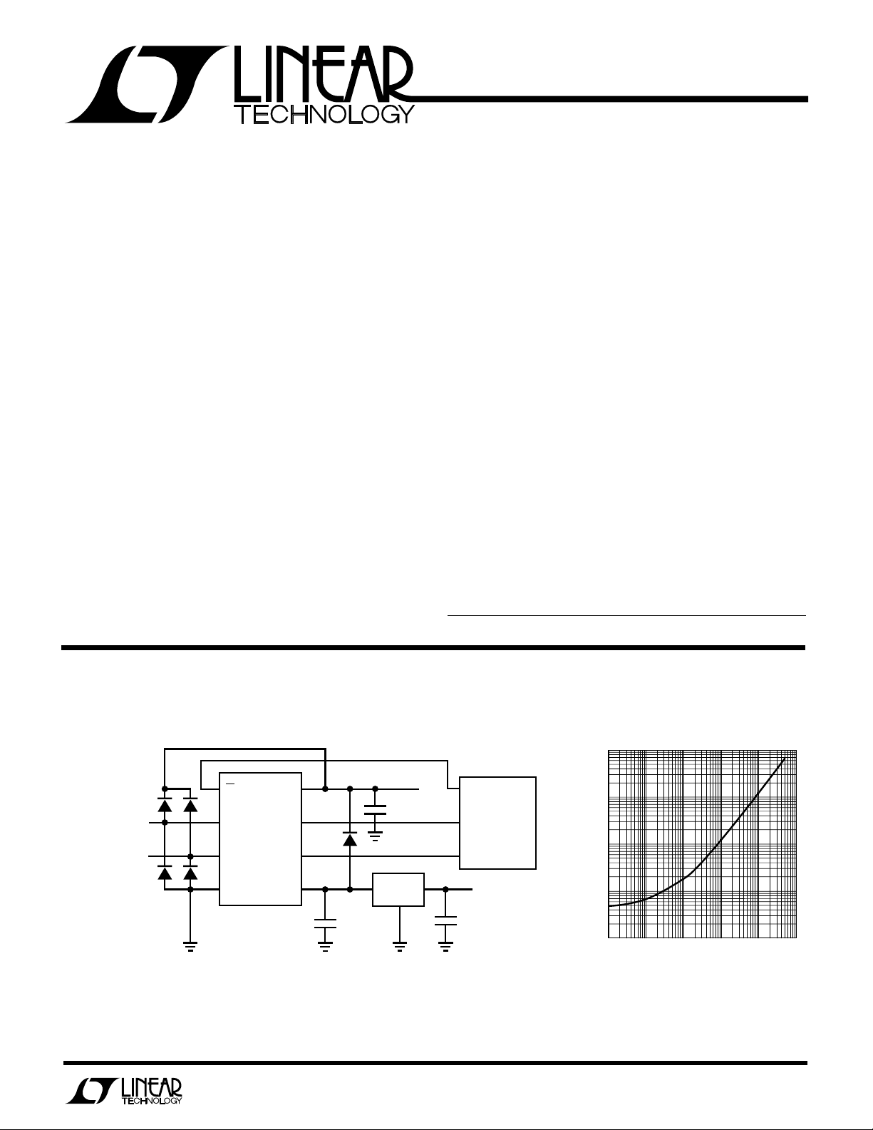
Single Chip 12-Bit
Data Acquisition Systems
EATU
F
■
Built-In Sample-and-Hold
■
Single Supply 5V Operation
■
60kHz Maximum Throughput Rate (LTC1292)
■
Power Shutdown After Each Conversion (LTC1297)
■
Direct 3-Wire Interface to Most MPU Serial Ports and
RE
S
All MPU Parallel Ports
■
Analog Inputs Common Mode to Supply Rails
U
KEY SPECIFICATIO S
■
Resolution: 12 Bits
■
Fast Conversion Time: 12µs Max Over Temp
■
Low Supply Current: 6.0mA
■
Shutdown Supply Current: 5µA (LTC1297)
DUESCRIPTIO
The LTC1292/LTC1297 are data acquisition systems that
contain a 12-bit, switched-capacitor successive approximation A/D, a differential input, sample-and-hold on the
(+) input, and serial I/O. When the LTC1297 is idle between
conversions it automatically powers down reducing the
supply current to 5µA, typically. The LTC1292 is capable
of digitizing signals at a 60kHz rate and with the device’s
excellent AC characteristics, it can be used for DSP applications. All these features are packaged in an 8-pin DIP
and are made possible using LTCMOSTM switched-capacitor technology.
The serial I/O is designed to communicate without external
hardware to most MPU serial ports and all MPU parallel
I/O ports allowing data to be transmitted over three wires.
Because of their accuracy, ease of use and small package
size these devices are well suited for digitizing analog
signals in remote applications where minimum number of
interconnects and power consumption are important.
LTCMOS is trademark of Linear Technology Corporation
DIFFERENTIAL
INPUTS
COMMON MODE
RANGE
0V TO 5V
U
O
A
PPLICATITYPICAL
12-Bit Differential Input Data Acquisition System
LTC1297
V
CC
CLK
1N4148
D
OUT
V
REF
+
AND GND WITH 1N4148 DIODES.
CC
+
4.7µF
TANTALUM
22µF
TANTALUM
LT1027
CS
+
–
*
*FOR OVERVOLTAGE PROTECTION LIMIT THE INPUT CURRENT TO 15mA
PER PIN OR CLAMP THE INPUTS TO V
CONVERSION RESULTS ARE NOT VALID WHEN ANY INPUT IS OVERVOLTAGED
< GND OR V
(V
IN
THE APPLICATIONS INFORMATION.
+IN
–IN
GND
> VCC). SEE SECTION ON OVERVOLTAGE PROTECTION IN
IN
Power Supply Current
vs Sampling Frequency
DO
5V
MC68HC11
SCK
MISO
8V TO 40V
1µF
LTC1292/7 TA01
1
LTC1292/LTC1297
O
A
(Notes 1 and 2)
LUTEXI T
S
W
A
WUW
ARB
U
G
I
S
Supply Voltage (VCC) to GND.................................. 12V
Voltage
Analog and Reference
Inputs..................................... –0.3V to V
CC
+ 0.3V
Digital Inputs........................................ –0.3V to 12V
Digital Outputs .......................... –0.3V to V
CC
+ 0.3V
Power Dissipation.............................................. 500mW
Operating Temperature Range
LTC1292/LTC1297BC, LTC1292/LTC1297CC,
LTC1292/LTC1297DC ............................ 0°C to 70°C
LTC1292/LTC1297BI, LTC1292/LTC1297CI,
LTC1292/LTC1297DI ........................ –40°C to 85°C
Storage Temperature Range ................ –65°C to 150°C
Lead Temperature (Soldering, 10 sec.)................ 300°C
/
PACKAGE
O
RDER I FOR ATIO
ORDER PART NUMBER
TOP VIEW
LTC1292BIN8 LTC1297BIN8
V
CC
LTC1292CIN8 LTC1297CIN8
CLK
LTC1292DIN8 LTC1297DIN8
D
OUT
LTC1292BCJ8 LTC1297BCJ8
V
REF
LTC1292CCJ8 LTC1297CCJ8
LTC1292DCJ8 LTC1297DCJ8
LTC1292BCN8 LTC1297BCN8
LTC1292CCN8 LTC1297CCN8
LTC1292DCN8 LTC1297DCN8
=100°C/W (J8)
JA
=130°C/W (N8)
JA
8
7
6
5
1
CS
2
+IN
3
–IN
4
GND
J8 PACKAGE
8-LEAD CERAMIC DIP
N8 PACKAGE
8-LEAD PLASTIC DIP
T
= 150°C, θ
JMAX
= 100°C, θ
T
JMAX
For Military Temperature Ranges please contact factory.
WU
U
UU W
CO VERTER A D ULTIPLEXER CHARACTERISTICS
LTC1292B
LTC1297B
PARAMETER CONDITIONS MIN TYP MAX MIN TYP MAX MIN TYP MAX UNITS
Offset Error (Note 4) ● ±3.0 ±3.0 ±3.0 LSB
Linearity Error (INL) (Note 4 & 5) ● ±0.5 ±0.5 ±0.75 LSB
Gain Error (Note 4) ● ±0.5 ±1.0 ±4.0 LSB
Minimum Resolution for Which No 12 12 12 Bits
Missing Codes are Guaranteed
Analog and REF Input Range (Note 7) ● –0.05V to VCC + 0.05V V
On Channel Leakage Current On Channel = 5V ● ±1 ±1 ±1 µA
(Note 8) Off Channel = 0V
On Channel = 0V ● ±1 ±1 ±1 µA
Off Channel = 5V
Off Channel Lekage Current On Channel = 5V ● ±1 ±1 ±1 µA
(Note 8) Off Channel = 0V
On Channel = 0V ● ±1 ±1 ±1 µA
Off Channel = 5V
(Note 3)
LTC1292C
LTC1297C
LTC1292D
LTC1297D
2
LTC1292/LTC1297
AC CHARACTERISTICS
(Note 3)
LTC1292B/LTC1297B
LTC1292C/LTC1297C
LTC1292D/LTC1297D
SYMBOL PARAMETER CONDITIONS MIN TYP MAX UNITS
f
CLK
t
SMPL
Clock Frequency VCC = 5V (Note 6) (Note 9) 1.0 MHz
Analog Input Sample Time See Operating Sequence LTC1292 1.5CLK
LTC1297 0.5CLK+5.5µs
t
CONV
Conversion Time See Operating Sequence 12 CLK
Cycles
t
CYC
Total Cycle Time See Operating Sequence (Note 6)
LTC1292 14CLK+2.5µs
LTC1297 14CLK+6µs
t
dDO
t
dis
t
en
t
hDO
t
f
t
r
t
WHCLK
t
WLCLK
t
suCS
Delay Time, CLK↓ to D
Delay Time, CS↑ to D
Delay Time, CLK↓ to D
Data Valid See Test Circuits ● 160 300 ns
OUT
Hi-Z See Test Circuits ● 80 150 ns
OUT
Enabled See Test Circuits ● 80 200 ns
OUT
Time Output Data Remains Valid After CLK↓ 130 ns
D
Fall Time See Test Circuits ● 65 130 ns
OUT
D
Rise Time See Test Circuits ● 25 50 ns
OUT
CLK High Time VCC = 5V (Note 6) 300 ns
CLK Low Time VCC = 5V (Note 6) 400 ns
Setup Time, CS↓ Before CLK↑ VCC = 5V (Note 6) LTC1292 50 ns
(LTC1297 Wakeup Time) LTC1297 5.5 µs
t
WHCS
CS High Time Between Data Transfer Cycles VCC = 5V (Note 6) LTC1292 2.5 µs
LTC1297 0.5 µs
t
WLCS
CS Low Time During Data Transfer VCC = 5V (Note 6) LTC1292 14CLK
LTC1297 14CLK+5.5µs
C
IN
Input Capacitance Analog Inputs On Channel 100 pF
Analog Inputs Off Channel 5 pF
Digital Inputs 5 pF
U
DIGITAL A D DC ELECTRICAL CHARACTERISTICS
SYMBOL PARAMETER CONDITIONS MIN TYP MAX UNITS
V
IH
V
IL
I
IH
I
IL
V
OH
V
OL
I
OZ
I
SOURCE
I
SINK
High Level Input Voltage VCC = 5.25V ● 2.0 V
Low Level Input Voltage VCC = 4.75V ● 0.8 V
High Level Input Current VIN = V
CC
Low Level Input Current VIN = 0V ● –2.5 µA
High Level Output Voltage VCC = 4.75V, IO = –10µA 4.7 V
IO = 360µA ● 2.4 4.0 V
Low Level Output Voltage VCC = 4.75V, IO = 1.6mA ● 0.4 V
High Z Output Leakage V
Output Source Current V
Output Sink Current V
= VCC, CS High ● 3 µA
OUT
V
= 0V, CS High ● –3 µA
OUT
= 0V –20 mA
OUT
= V
OUT
CC
(Note 3)
LTC1292B/LTC1297B
LTC1292C/LTC1297C
LTC1292D/LTC1297D
● 2.5 µA
20 mA
3
LTC1292/LTC1297
U
DIGITAL A D DC ELECTRICAL CHARACTERISTICS
SYMBOL PARAMETER CONDITIONS MIN TYP MAX UNITS
I
CC
I
REF
The ● denotes specifications which apply over the operating temperature
range; all other limits and typicals T
Note 1: Absolute Maximum Ratings are those values beyond which the life
of a device may be impaired.
Note 2: All voltage values are with respect to ground (unless otherwise
noted).
Note 3: V
Note 4: One LSB is equal to V
= 5V, 1LSB = 5V/4096 = 1.22mV.
Note 5: Linearity error is specified between the actual end points of the
A/D transfer curve. The deviation is measured from the center of the
quantization band.
Note 6: Recommended operating conditions.
Note 7: Two on-chip diodes are tied to each reference and analog input
which will conduct for reference or analog input voltages one diode drop
Positive Supply Current CS High LTC1292 ● 612 mA
CS Low LTC1297 ● 612 mA
CS High
LTC1297BC, LTC1297CC, LTC1297DC ● 510 µA
Power
Shutdown
CLK Off
LTC1297BI, LTC1297CI, LTC1297DI ● 515 µA
LTC1297BM, LTC1297CM, LTC1297DM
Reference Current CS High ● 10 50 µA
below GND or one diode drop above VCC. Be careful during testing at low
= 25°C.
A
levels (4.5V), as high level reference or analog inputs (5V) can cause
V
CC
this input diode to conduct, especially at elevated temperatures, and cause
errors for inputs near full scale. This spec allows 50mV forward bias of
either diode. This means that as long as the reference or analog input does
not exceed the supply voltage by more than 50mV, the output code will be
= 5V, V
CC
= 5V, CLK = 1.0MHz unless otherwise specified.
REF
divided by 4096. For example, when V
REF
correct. To achieve an absolute 0V to 5V input voltage range will therefore
require a minimum supply voltage of 4.950V over initial tolerance,
REF
temperature variations and loading.
Note 8: Channel leakage current is measured after the channel selection.
Note 9: Increased leakage currents at elevated temperatures cause the S/
H to droop, therefore it is recommended that f
≥ 31kHz at 85°C, and f
(Note 3)
≥ 3kHz at 25°C.
CLK
LTC1292B/LTC1297B
LTC1292C/LTC1297C
LTC1292D/LTC1297D
≥125kHz at 125°C, f
CLK
CLK
LPER
10
CLK = 1MHz
= 25°C
T
A
8
6
4
SUPPLY CURRENT (mA)
2
0
4
SUPPLY VOLTAGE (V)
5
F
O
R
ATYPICA
LTC1292/7 G01
UW
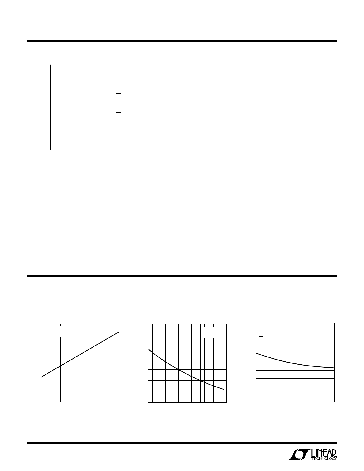
CCHARA TERIST
E
C
Supply Current vs TemperatureSupply Current vs Supply Voltage
10
9
8
7
6
5
SUPPLY CURRENT (mA)
4
6
3
–50
–30 –10
ICS
CLK = 1MHz
V
CC
10
AMBIENT TEMPERATURE (°C)
50 90
30 70
= 5V
110
LTC1292/7 G02
130
LTC1297 Supply Current (Power
Shutdown) vs Temperature
10
VCC = 5V
9
= 5V
V
REF
CS HIGH
8
CLK OFF
7
6
5
4
3
SUPPLY CURRENT (µA)
2
1
0
–50
0
–25
AMBIENT TEMPERATURE (°C)
50
25
75
100
LTC1292/7 G03
125
4
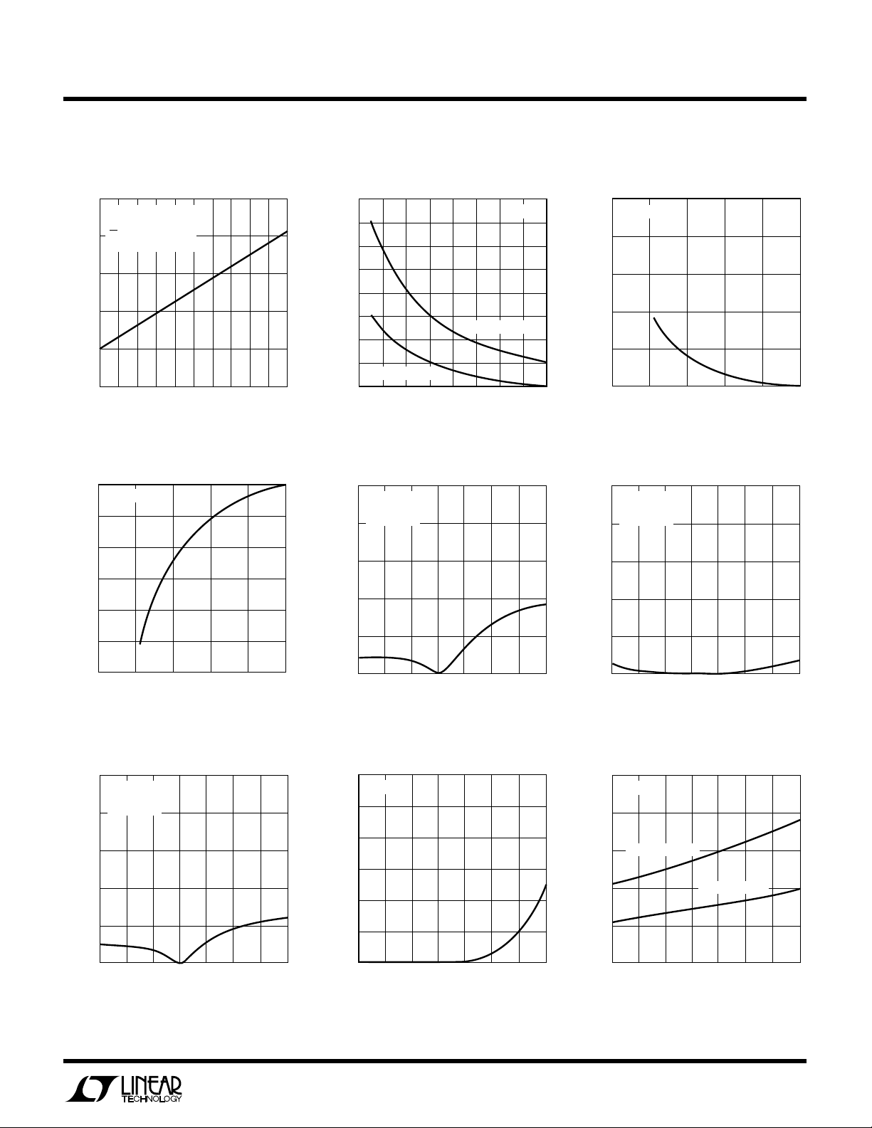
LPER
REFERENCE VOLTAGE (V)
0
LINEARITY (LSB = 1/4096 × V
REF
)
0.75
1.00
1.25
4
LTC1292/7 G06
0.50
0.25
0
1
2
3
5
VCC = 5V
AMBIENT TEMPERATURE (°C)
–50
MAGNITUDE OF LINEARITY CHANGE (LSB)
0.3
0.4
0.5
50
LTC1292/7 G09
0.2
0.1
0
–25
0
25
75
125100
VCC = 5V
V
REF
= 5V
CLK = 1MHz
F
O
R
ATYPICA
UW
CCHARA TERIST
E
C
LTC1292/LTC1297
ICS
LTC1297 Supply Current (Power
Shutdown) vs CLK Frequency
25
VCC = 5V
= 5V
V
REF
CS HIGH
20
CMOS LOGIC LEVELS
15
10
SUPPLY CURRENT (µA)
5
0
200
0
CLK FREQUENCY (kHz)
400
600
800
LTC1292/7 G04
1000
Unadjusted Offset Voltage vs
Reference Voltage
0.9
0.8
)
REF
0.7
0.6
0.5
0.4
0.3
OFFSET (LSB = 1/4096 × V
0.2
V
= 0.125mV
OS
0.1
1
2
REFERENCE VOLTAGE (V)
3
V
OS
Change in Gain vs
Reference Voltage Change in Offset vs Temperature
)
REF
–0.2
–0.4
–0.6
–0.8
0
V
= 5V
CC
0.5
0.4
0.3
0.2
VCC = 5V
= 5V
V
REF
CLK = 1MHz
VCC = 5V
= 0.250mV
4
LTC1292/7 G05
Change in Linearity vs
Reference Voltage
5
Change in Linearity vs
Temperature
–1.0
CHANGE IN GAIN (LSB = 1/4096 × V
–1.2
0
1234
REFERENCE VOLTAGE (V)
Change in Gain vs Temperature
0.5
VCC = 5V
= 5V
V
REF
CLK = 1MHz
0.4
0.3
0.2
0.1
MAGNITUDE OF GAIN CHANGE (LSB)
0
–50
* AS THE CLK FREQUENCY IS DECREASED FROM 1MHz, MINIMUM CLK FREQUENCY (∆ERROR ≤ 0.1LSB) REPRESENTS THE
FREQUENCY AT WHICH A 0.1LSB SHIFT IN ANY CODE TRANSITION FROM ITS 1MHz VALUE IS FIRST DETECTED (NOTE 9).
0
–25
AMBIENT TEMPERATURE (°C)
25
0.1
MAGNITUDE OF OFFSET CHANGE (LSB)
5
LTC1292/7 G07
0
–50
0
–25
AMBIENT TEMPERATURE (°C)
25
50
75
125100
LTC1292/7 G08
Minimum Clock Rate for
D
0.1 LSB Error*
DELAY TIME FROM CLK↓ (ns)
OUT
D
250
200
150
100
VCC = 5V
0.25
0.20
0.15
0.10
0.05
MINIMUM CLK FREQUENCY (MHz)
–50
50
75
125100
LTC1292/7 G10
–25
25
50
0
AMBIENT TEMPERATURE (°C)
75
125100
LTC1292/7 G11
Delay Time vs Temperature
OUT
VCC = 5V
MSB FIRST DATA
LSB FIRST DATA
50
0
–50
–25
25
0
AMBIENT TEMPERATURE (°C)
50
75
125100
LTC1292/7 G12
5
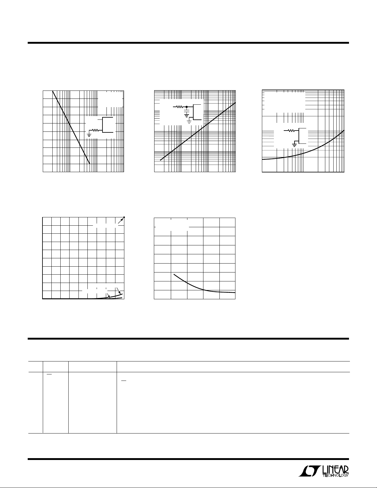
LTC1292/LTC1297
R
SOURCE
+ (Ω)
100
1
S & H AQUISITION TIME TO 0.02% (µs)
10
100
1000 10000
LTC1292/7 G15
+
–
+V
IN
R
SOURCE
V
REF
= 5V
V
CC
= 5V
T
A
= 25°C
0V TO 5V INPUT STEP
LPER
F
O
R
ATYPICA
UW
CCHARA TERIST
E
C
ICS
Maximum Clock Rate vs
Source Resistance
1.0
0.8
+V
0.6
0.4
0.2
MAXIMUM CLK FREQUENCY* (MHz)
0
100
1k 10k 100k
R
SOURCE
R
SOURCE
– (Ω)
IN
Input Channel Leakage Current vs
Temperature
1000
900
800
700
600
500
400
300
200
100
INPUT CHANNEL LEAKAGE CURRENT (nA)
0
–30 10
–10
–50
AMBIENT TEMPERATURE (°C)
GUARANTEED
ON CHANNEL
OFF CHANNEL
70 90
50 130
30
VCC = 5V
= 5V
V
REF
CLK = 1MHz
+
+IN
–IN
–
LTC1292/7G13
110
LTC1292/7 G16
Maximum Filter Resistor vs
Cycle Time
10k
R
FILTER
1k
** (Ω)
FILTER
100
10
MAXIMUM R
1
10
+V
C
FILTER
IN
≥1µF
+
–
100
CYCLE TIME (µs)
1k
Noise Error vs Reference Voltage
2.25
LTC1292/LTC1297
2.00
NOISE = 200µV
1.75
1.50
1.25
1.00
0.75
0.50
PEAK-TO-PEAK NOISE ERROR (LSB)
0.25
0
0
P-P
13
2
REFERENCE VOLTAGE (V)
LTC1292/7 G14
4
LTC1292/7 G17
10k
Sample-and-Hold Acquisition
Time vs Source Resistance
* MAXIMUM CLK FREQUENCY REPRESENTS THE
CLK FREQUENCY AT WHICH A 0.1LSB SHIFT IN
THE ERROR AT ANY CODE TRANSITION FROM ITS
1MHz VALUE IS FIRST DETECTED.
** MAXIMUM R
RESISTOR VALUE AT WHICH A 0.1LSB CHANGE IN
FULL SCALE ERROR FROM ITS VALUE AT
R
= 0Ω IS FIRST DETECTED.
FILTER
5
REPRESENTS THE FILTER
FILTER
U
PI FU CTIO S
# PIN FUNCTION DESCRIPTION
1 CS Chip Select Input A logic low on this input enables the LTC1292/LTC1297. Power shutdown is activated on the LTC1297 when
2, 3 +IN, –IN Analog Inputs These inputs must be free of noise with respect to GND.
4 GND Analog Ground GND should be tied directly to an analog ground plane.
5V
6D
7 CLK Shift Clock This clock synchronizes the serial data transfer.
8V
6
REF
OUT
CC
UU
CS is brought high.
Reference Input The reference input defines the span of the A/D converter and must be kept free of noise with respect to GND.
Digital Data Output The A/D conversion result is shifted out of this output.
Positive Supply This supply must be kept free of noise and ripple by bypassing directly to the analog ground plane.
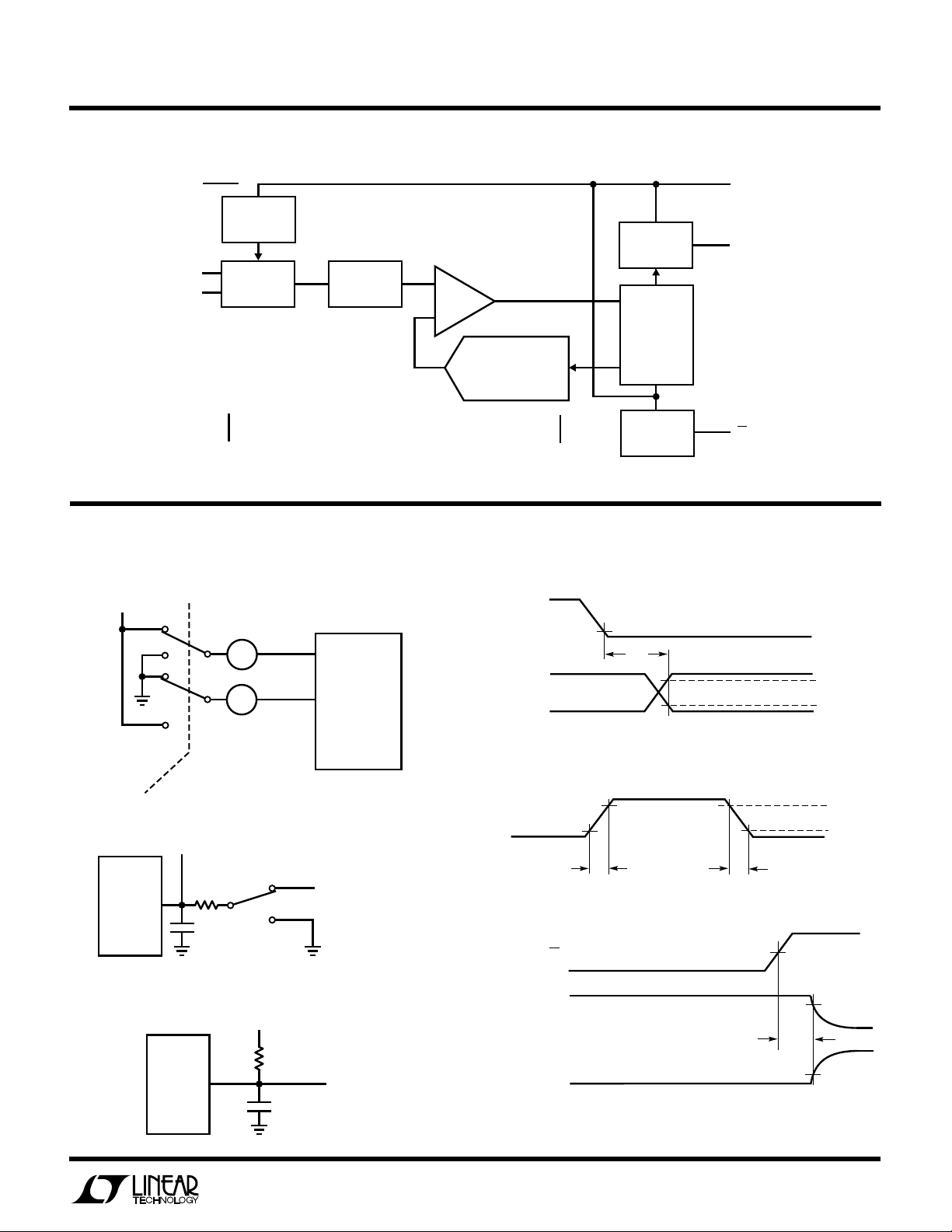
BLOCK
LTC1292/LTC1297
W
IDAGRA
8
V
CC
2
+IN
3
–IN
GND
TEST CIRCUITS
On and Off Channel Leakage Current
5V
INPUT
SHIFT
REGISTER
ANALOG
INPUT MUX
4
I
ON
A
I
OFF
A
SAMPLE
AND
HOLD
ON CHANNEL
OFF CHANNEL
COMP
12-BIT
CAPACITIVE
DAC
CLK
D
OUTPUT
SHIFT
REGISTER
12-BIT
SAR
5
V
REF
CONTROL
AND
TIMING
Voltage Waveforms for D
0.8V
t
dDO
OUT
7
CLK
6
D
OUT
1
CS
LTC1292/7 BD
Delay Time, t
OUT
dDO
2.4V
0.4V
LTC1292/7 TC04
POLARITY
Load Circuit for t
TEST POINT
D
OUT
Load Circuit for t
D
OUT
3k
100pF
1.4V
3kΩ
100pF
dis
dDO
and t
en
5V t
dis
t
WAVEFORM 1
dis
, tr and t
TEST POINT
LTC1292/7 TC01
WAVEFORM 2, t
LTC1292/7 TC02
f
LTC1292/7 TC03
Voltage Waveforms for D
D
OUT
t
r
en
Voltage Waveforms for t
CS
D
OUT
WAVEFORM 1
(SEE NOTE 1)
D
OUT
WAVEFORM 2
(SEE NOTE 2)
NOTE 1: WAVEFORM 1 IS FOR AN OUTPUT WITH INTERNAL CONDITIONS SUCH
THAT THE OUTPUT IS HIGH UNLESS DISABLED BY THE OUTPUT CONTROL.
LTC1292/7 TC06
NOTE 2: WAVEFORM 2 IS FOR AN OUTPUT WITH INTERNAL CONDITIONS SUCH
THAT THE OUTPUT IS LOW UNLESS DISABLED BY THE OUTPUT CONTROL.
Rise and Fall Times, tr, t
OUT
t
f
dis
2.0V
t
dis
f
2.4V
0.4V
LTC1292/7 TC05
90%
10%
7
LTC1292/LTC1297
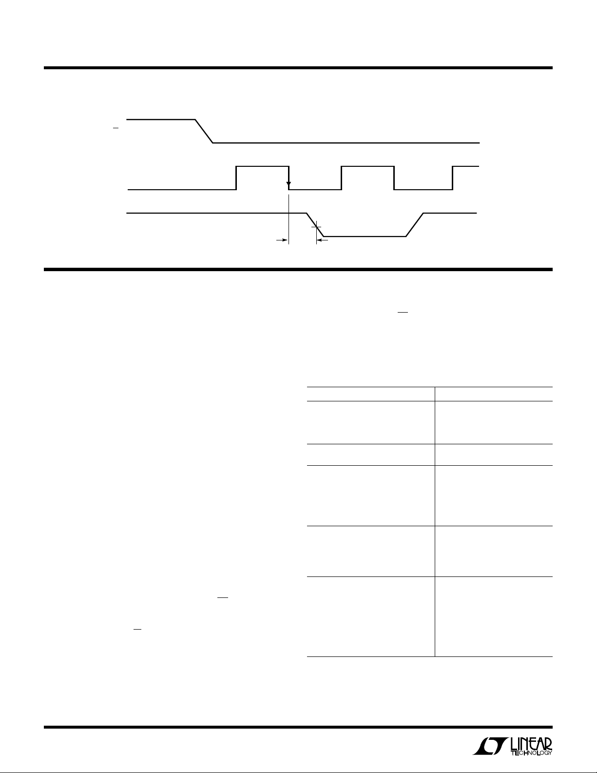
TEST CIRCUITS
Voltage Waveforms for t
CS
CLK
D
OUT
PPLICATI
A
U
O
S
I FOR ATIO
WU
U
The LTC1292/LTC1297 are data acquisition components
which contain the following functional blocks:
1. 12-Bit Succesive Approximation Capacitive A/D
Converter
2. Differential Input
3. Sample-and-Hold (S/H)
4. Synchronous, Half-Duplex Serial Interface
5. Control and Timing Logic
DIGITAL CONSIDERATIONS
Serial Interface
The LTC1292/LTC1297 communicate with microprocessors and other external circuitry via a synchronous, halfduplex, three-wire serial interface (see Operating Sequence). The clock (CLK) synchronizes the data transfer
with each bit being transmitted on the falling CLK edge.
The LTC1292/LTC1297 do not require a configuration
input word and have no DIN pin. They are permanently
configured to have a single differential input and to perform a unipolar conversion. A falling CS initiates data
transfer. To allow the LTC1297 to recover from the power
shutdown mode, t
pulse enables D
OUT
result is output on the D
has to be met. Then the first CLK
suCS
. After one null bit, the A/D conversion
line with a MSB-first sequence
OUT
followed by a LSB-first sequence. With the half-duplex
serial interface the D
data is from the current conver-
OUT
sion. This provides easy interface to MSB-first or LSB-first
en
0.8V
t
en
B11
LTC1292/7 TC07
serial ports. Bringing CS high resets the LTC1292/LTC1297
for the next data exchange and puts the LTC1297 into its
power shutdown mode.
Table 1. Microprocessor with Hardware Serial Interfaces
Compatible with the LTC1292/LTC1297**
PART NUMBER TYPE OF INTERFACE
Motorola
MC6805S2, S3 SPI
MC68HC11 SPI
MC68HC05 SPI
RCA
CDP68HC05 SPI
Hitachi
HD6305 SCI Synchronous
HD6301 SCI Synchronous
HD63701 SCI Synchronous
HD6303 SCI Synchronous
HD64180 SCI Synchronous
National Semiconductor
COP400 Family MICROWIRE
COP800 Family MCROWIRE/PLUS
NS8050U MICROWIRE/PLUS
HPC16000 Family MICROWIRE/PLUS
Texas Instruments
TMS7002 Serial Port
TMS7042 Serial Port
TMS70C02 Serial Port
TMS70C42 Serial Port
TMS32011* Serial Port
TMS32020* Serial Port
TMS370C050 SPI
* Requires external hardware
** Contact factory for interface information for processors not on this list
†
MICROWIRE and MICROWIRE/PLUS are trademarks of National
Semiconductor Corp.
†
†
8
 Loading...