FEATURES
LTC1069-6
Single Supply, Very Low
Power, Elliptic Lowpass Filter
U
DESCRIPTION
■
8th Order Elliptic Filter in SO-8 Package
■
Single 3V Operation: Supply Current: 1mA (Typ)
f
CUTOFF
: 14kHz (Max)
S/N Ratio: 72dB
■
Single 5V Operation: Supply Current: 1.2mA (Typ)
f
CUTOFF
: 20kHz (Max)
S/N Ratio: 79dB
■
±0.1dB Passband Ripple Up to 0.9f
■
42dB Attenuation at 1.3f
■
66dB Attenuation at 2.0f
■
70dB Attenuation at 2.1f
■
Wide Dynamic Range, 75dB or More (S/N + THD),
CUTOFF
CUTOFF
CUTOFF
CUTOFF
(Typ)
Under Single 5V Operation
■
Wideband Noise: 120µV
■
Clock-to-f
■
Internal Sample Rate: 100:1
CUTOFF
Ratio: 50:1
RMS
U
APPLICATIONS
■
Handheld Instruments
■
Telecommunication Filters
■
Antialiasing Filters
■
Smoothing Filters
■
Audio
■
Multimedia
The LTC®1069-6 is a monolithic low power, 8th order lowpass filter optimized for single 3V or single 5V supply
operation. The LTC1069-6 typically consumes 1mA under
single 3V supply operation and 1.2mA under 5V operation.
The cutoff frequency of the LTC1069-6 is clock tunable and it
is equal to the clock frequency divided by 50. The input signal
is sampled twice per clock cycle to lower the risk of aliasing.
The typical passband ripple is ± 0.1dB up to 0.9f
The gain at f
is –0.7dB. The transition band of the
CUTOFF
CUTOFF
.
LTC1069-6 features progressive attenuation reaching 42dB
at 1.3f
and 70dB at 2.1f
CUTOFF
. The maximum
CUTOFF
stopband attenuation is 72dB.
The LTC1069-6 can be clock tuned for cutoff frequencies
up to 20kHz (single 5V supply) and for cutoff frequencies
up to 14kHz (single 3V supply).
The low power feature of the LTC1069-6 does not penalize
the device’s dynamic range. With single 5V supply and an
input range of 0.4V
RMS
to 1.4V
, the Signal-to-(Noise
RMS
+ THD) ratio is ≥70dB. The wideband noise of the
LTC1069-6 is 125µV
RMS
.
Other filter responses with higher speed can be obtained.
Please contact LTC Marketing for details.
The LTC1069-6 is available in an 8-pin SO package.
, LTC and LT are registered trademarks of Linear Technology Corporation.
TYPICAL APPLICATION
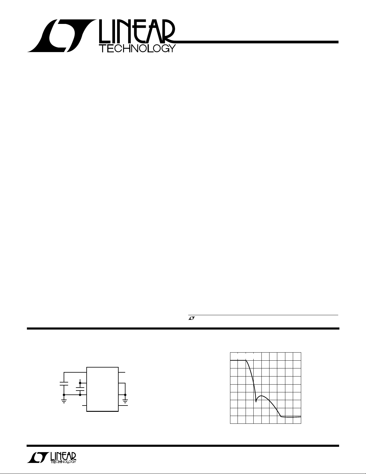
Single 3V Supply 10kHz Elliptic Lowpass Filter
0.47µF
0.1µF
AGND
3V
+
V
NC
V
IN
LTC1069-6
V
OUT
–
V
NC
CLK
U
f
CLK
= 500kHz
1069-6 TA01
10
0
–10
–20
–30
–40
GAIN (dB)
–50
–60
–70
–80
5
Frequency Response
VIN = 500mV
RMS
10 20 25
15
FREQUENCY (kHz)
1069-6 TA02
1

LTC1069-6
1
2
3
4
8
7
6
5
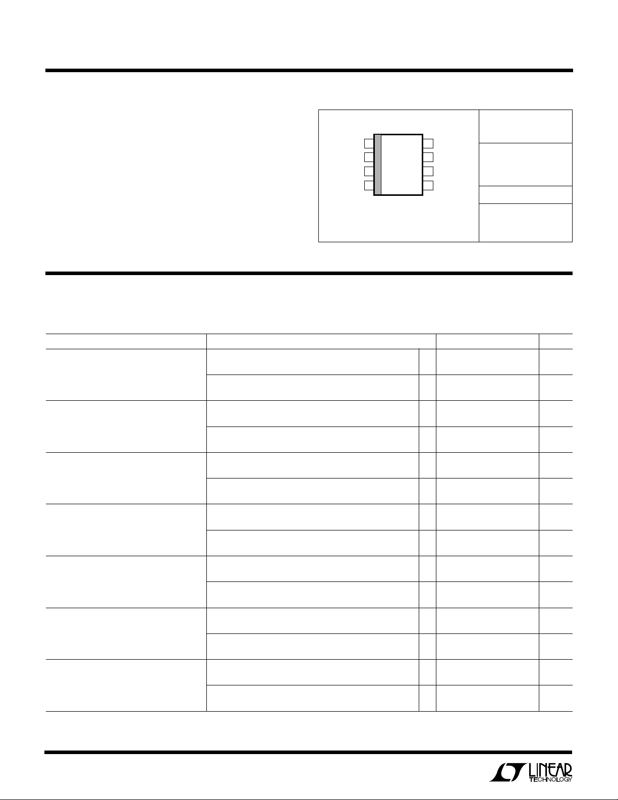
TOP VIEW
V
OUT
V
–
NC
CLK
AGND
V
+
NC
V
IN
S8 PACKAGE
8-LEAD PLASTIC SO
WW
W
ABSOLUTE MAXIMUM RATINGS
Total Supply Voltage (V+ to V–) .............................. 12V
Operating Temperature Range
U
U
W
PACKAGE/ORDER INFORMATION
ORDER PART
NUMBER
LTC1069-6C ............................................ 0°C to 70°C
LTC1069-6I ........................................ – 40°C to 85°C
Storage Temperature ............................ – 65°C to 150°C
LTC1069-6CS8
LTC1069-6IS8
Lead Temperature (Soldering, 10 sec).................. 300°C
S8 PART MARKING
T
= 125°C, θJA = 110°C/ W
JMAX
Consult factory for Military grade parts.
10696
10696I
ELECTRICAL CHARACTERISTICS
f
is the filter’s cutoff frequency and is equal to f
CUTOFF
/50. The f
CLK
signal level is TTL or CMOS (clock rise or fall time ≤1µs)
CLK
RL = 10k, VS = 5V, TA = 25°C, unless otherwise specified. All AC gains are measured relative to the passband gain.
PARAMETER CONDITIONS MIN TYP MAX UNITS
Passband Gain (fIN ≤ 0.2f
Gain at 0.50f
Gain at 0.75f
Gain at 0.90f
Gain at 0.95f
Gain at f
Gain at 1.30f
CUTOFF
CUTOFF
CUTOFF
CUTOFF
CUTOFF
CUTOFF
)V
CUTOFF
= 5V, f
S
f
TEST
VS = 3V, f
f
TEST
VS = 5V, f
f
TEST
VS = 3V, f
f
TEST
VS = 5V, f
f
TEST
VS = 3V, f
f
TEST
VS = 5V, f
f
TEST
VS = 3V, f
f
TEST
VS = 5V, f
f
TEST
VS = 3V, f
f
TEST
VS = 5V, f
f
TEST
VS = 3V, f
f
TEST
VS = 5V, f
f
TEST
VS = 3V, f
f
TEST
= 200kHz –0.25 0.1 0.45 dB
CLK
= 0.25kHz, VIN = 1V
= 200kHz –0.25 0.1 0.45 dB
CLK
= 0.25kHz, VIN = 0.5V
= 200kHz –0.10 0.07 0.25 dB
CLK
= 2.0kHz, VIN = 1V
= 200kHz –0.15 0.07 0.25 dB
CLK
= 2.0kHz, VIN = 0.5V
= 200kHz –0.25 0 0.25 dB
CLK
= 3.0kHz, VIN = 1V
= 200kHz –0.25 0 0.25 dB
CLK
= 3.0kHz, VIN = 0.5V
= 200kHz –0.25 0.1 0.45 dB
CLK
= 3.6kHz, VIN = 1V
= 200kHz –0.25 0.1 0.45 dB
CLK
= 3.6kHz, VIN = 0.5V
= 200kHz –0.35 0.05 0.25 dB
CLK
= 3.8kHz, VIN = 1V
= 200kHz –0.45 0.05 0.25 dB
CLK
= 3.8kHz, VIN = 0.5V
= 200kHz –1.50 –0.07 –0.20 dB
CLK
= 4.0kHz, VIN = 1V
= 200kHz –1.5 –0.07 0 dB
CLK
= 4.0kHz, VIN = 0.5V
= 200kHz –42 – 40 dB
CLK
= 5.2kHz, VIN = 1V
= 200kHz –41 – 38 dB
CLK
= 5.2kHz, VIN = 0.5V
RMS
RMS
RMS
RMS
RMS
RMS
RMS
RMS
RMS
RMS
RMS
RMS
RMS
RMS
● –0.30 0.1 0.50 dB
● –0.30 0.1 0.50 dB
● –0.15 0.07 0.30 dB
● –0.20 0.07 0.30 dB
● –0.30 0 0.30 dB
● –0.30 0 0.30 dB
● –0.25 0.1 0.45 dB
● –0.30 0.1 0.50 dB
● –0.45 0.05 0.25 dB
● –0.55 0.05 0.35 dB
● –1.65 –0.07 –0.25 dB
● –1.7 –0.07 0 dB
● –42 –39 dB
● –41 – 37 dB
2
U

LTC1069-6
FREQUENCY (kHz)
20
–80
GAIN (dB)
–78
–74
–72
–70
–60
–66
40
60
1069-6 G03
–76
–64
–62
–68
80
100
VS = SINGLE 3V
f
CLK
= 500kHz
f
CUTOFF
= 10kHz
V
IN
= 0.5V
RMS
ELECTRICAL CHARACTERISTICS
f
is the filter’s cutoff frequency and is equal to f
CUTOFF
RL = 10k, VS = 5V, TA = 25°C, unless otherwise specified. All AC gains are measured relative to the passband gain.
PARAMETER CONDITIONS MIN TYP MAX UNITS
Gain at 2.00f
Gain at 0.95f
CUTOFF
CUTOFF
Output DC Offset (Note 1) VS = 5V, f
Output DC Offset Tempco VS = 5V, VS = 3V 30 µV/°C
Output Voltage Swing (Note 2) VS = 5V, f
Power Supply Current VS = 5V, f
Maximum Clock Frequency VS = 5V 1.0 MHz
Input Frequency Range 0 <(f
Input Resistance 35 50 80 kΩ
Operating Supply Voltage (Note 3) 310V
VS = 5V, f
= 8.0kHz, VIN = 1V
f
TEST
VS = 3V, f
= 8.0kHz, VIN = 0.5V
f
TEST
VS = 5V, f
= 3V, f
V
S
= 3V, f
V
S
VS = 3V, f
VS = 3V, f
= 3V 0.7 MHz
V
S
/50. The f
CLK
= 200kHz –66 –61 dB
CLK
RMS
= 200kHz –66 –60 dB
CLK
= 400kHz, f
CLK
= 400kHz, f
CLK
= 100kHz 50 175 mV
CLK
= 100kHz 30 135 mV
CLK
= 100kHz 3.4 4.2 V
CLK
= 100kHz 1.6 2.0 V
CLK
= 100kHz 1.2 1.60 mA
CLK
= 100kHz 1.0 1.40 mA
CLK
signal level is TTL or CMOS (clock rise or fall time ≤1µs)
CLK
● –66 –60 dB
RMS
= 7.6kHz, VIN = 1V
TEST
= 7.6kHz, VIN = 0.5V
TEST
RMS
RMS
● –66 –59 dB
–0.5 0.15 0.5 dB
–0.5 0 0.5 dB
● 3.2 4.2 V
● 1.5 2.0 V
● 1.65 mA
● 1.55 mA
CLK
– 2fC)
P-P
P-P
P-P
P-P
The ● denotes specifications which apply over the full operating
temperature range.
Note 1: The input offset voltage is measured with respect to AGND (Pin 1).
The input (Pin 4) is also shorted to the AGND pin. The analog ground pin
potential is internally set to (0.437)(V
SUPPLY
).
Note 2: The input voltage can swing to either rail (V+ or ground); the
output typically swings 50mV from ground and 0.8V from V
Note 3: The LTC1069-6 is optimized for 3V and 5V operation. Although the
device can operate with a single 10V supply or ±5V, the total harmonic
distortion will be degraded. For single 10V or ±5V supply operation we
recommend to use the LTC1069-1.
W
U
TYPICAL PERFORMANCE CHARACTERISTICS
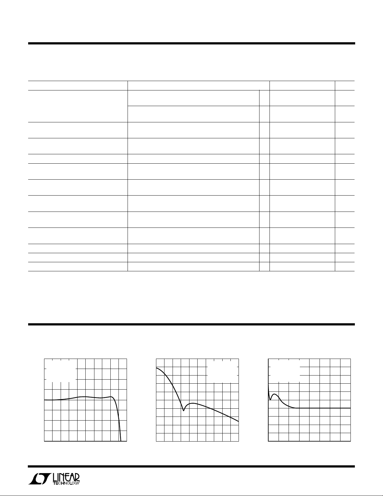
Transition Band Gain vs Frequency
10
0
–10
–20
–30
–40
GAIN (dB)
–50
–60
–70
–80
–90
12
10
FREQUENCY (kHz)
16
14
2
1
0
GAIN (dB)
–1
–2
Passband Gain vs Frequency
VS = SINGLE 3V
= 500kHz
f
CLK
= 10kHz
f
CUTOFF
= 0.5V
V
IN
RMS
3
1
FREQUENCY (kHz)
7
5
9
11
1069-6 G01
VS = SINGLE 3V
= 500kHz
f
CLK
= 10kHz
f
CUTOFF
= 0.5V
V
IN
RMS
18
1069-6 G02
+
.
Stopband Gain vs Frequency
20
3

LTC1069-6
FREQUENCY (kHz)
1
–90
GAIN (db)
–70
–50
–30
–10
10 100
1069-6 G06
10
–80
–60
–40
–20
0
f
CLK
= 500kHz
V
IN
= 0.5V
RMS
SINGLE 5V
SINGLE 3V
W
U
TYPICAL PERFORMANCE CHARACTERISTICS
Passband Gain vs Clock Frequency
2
VS = SINGLE 3V
= 0.5V
V
IN
RMS
1
f
CLK
f
CUTOFF
= 750kHz
= 15kHz
Passband Gain vs Clock Frequency
2
VS = SINGLE 5V
= 1V
V
IN
RMS
1
Amplitude Response
vs Supply Voltage
0
GAIN (dB)
f
= 500kHz
–1
–2
CLK
f
CUTOFF
5
3
1
Phase vs Frequency
90
0
–90
–180
–270
–360
–450
PHASE (DEG)
–540
–630
–720
–810
–900
0
2
= 10kHz
11
9
7
FREQUENCY (kHz)
4
6
FREQUENCY (kHz)
13
15
17 19
VS = SINGLE 5V
= 500kHz
f
CLK
= 10kHz
f
CUTOFF
8
10
1069-6 G04
12
1069-6 G07
0
GAIN (dB)
–1
–2
3
21
1
Group Delay vs Frequency
4.00E-04
3.50E-04
3.00E-04
2.50E-04
2.00E-04
1.50E-04
GROUP DELAY (SEC)
1.00E-04
5.00E-05
14
0.00E+00
0
f
CLK
500kHz
f
CUTOFF
10kHz
5
7
FREQUENCY (kHz)
VS = SINGLE 5V
= 500kHz
f
CLK
= 10kHz
f
CUTOFF
24 8
f
CLK
750kHz
f
CUTOFF
15kHz
13
11
9
6
FREQUENCY (kHz)
f
CLK
1MHz
f
CUTOFF
20kHz
15
17 19
1069-6 G05
21
Transient Response
0.5V/DIV
1069-6 G09
10
1069-6 G08
VS = SINGLE 5V 0.1ms/DIV
= 1MHz
f
CLK
f
= 1kHz
IN
2V
SQUAREWAVE
12
P-P
Dynamic Range THD + Noise
vs Input/Output Voltage
–40
f
= 170kHz
CLK
–45
–50
–55
–60
–65
–70
THD + NOISE (dB)
–75
–80
–85
–90
4
= 3.4kHz
f
CUTOFF
= 1kHz
f
IN
0.1
INPUT/OUTPUT VOLTAGE (V
VIN = 2.945V
P-P
13
)
P-P
1069-6 G14
Dynamic Range THD + Noise
vs Input Voltage
–40
f
= 500kHz
CLK
–45
= 1kHz
f
IN
–50
–55
–60
–65
–70
THD + NOISE (dB)
–75
–80
–85
–90
0.1 0.5 0.76 1.43
= SINGLE 3V
V
S
INPUT VOLTAGE (V
–40
–45
–50
–55
VS =
SINGLE 5V
15
)
RMS
1069-6 G10
–60
–65
–70
THD + NOISE (dB)
–75
–80
–85
–90
THD + Noise vs Frequency
f
= 500kHz
CLK
= 10kHz
f
CUTOFF
= SINGLE 3V
V
S
= 0.5V
V
IN
RMS
VS = SINGLE 5V
= 1V
V
IN
RMS
1510
FREQUENCY (kHz)
1069-6 G11

W
U
TYPICAL PERFORMANCE CHARACTERISTICS
Supply Current vs Supply Voltage
5
4.5
4
3
2
SUPPLY CURRENT (mA)
1
0
0
26
4
TOTAL SUPPLY VOLTAGE (V)
25°C
85°C
–40°C
14
8
12
10
16
1069-6 G12
4.0
2.5
2.0
POSITIVE SWING (V)NEGATIVE SWING (mV)
80
60
40
20
0
UUU
PIN FUNCTIONS
Output Voltage Swing
vs Temperature
RL = 10k
V
= SINGLE 5V
S
= SINGLE 3V
V
S
= SINGLE 3V
V
S
V
= SINGLE 5V
S
–40–200 20406080
AMBIENT TEMPERATURE (°C)
1069-6 G13
LTC1069-6
AGND (Pin 1): Analog Ground. The quality of the analog
signal ground can affect the filter performance. For either
single or dual supply operation, an analog ground plane
surrounding the package is recommended. The analog
ground plane should be connected to any digital ground at
a single point. For single supply operation, Pin 1 should be
bypassed to the analog ground plane with a 0.47µ F capacitor or larger. An internal resistive divider biases Pin 1 to
0.4366 times the total power supply of the device (Figure
1). That is, with a single 5V supply, the potential at Pin 1
is 2.183V ±1%. As the LTC1069-6 is optimized for single
supply operation, the internal biasing of Pin 1 allows
optimum output swing. The AGND pin should be buffered
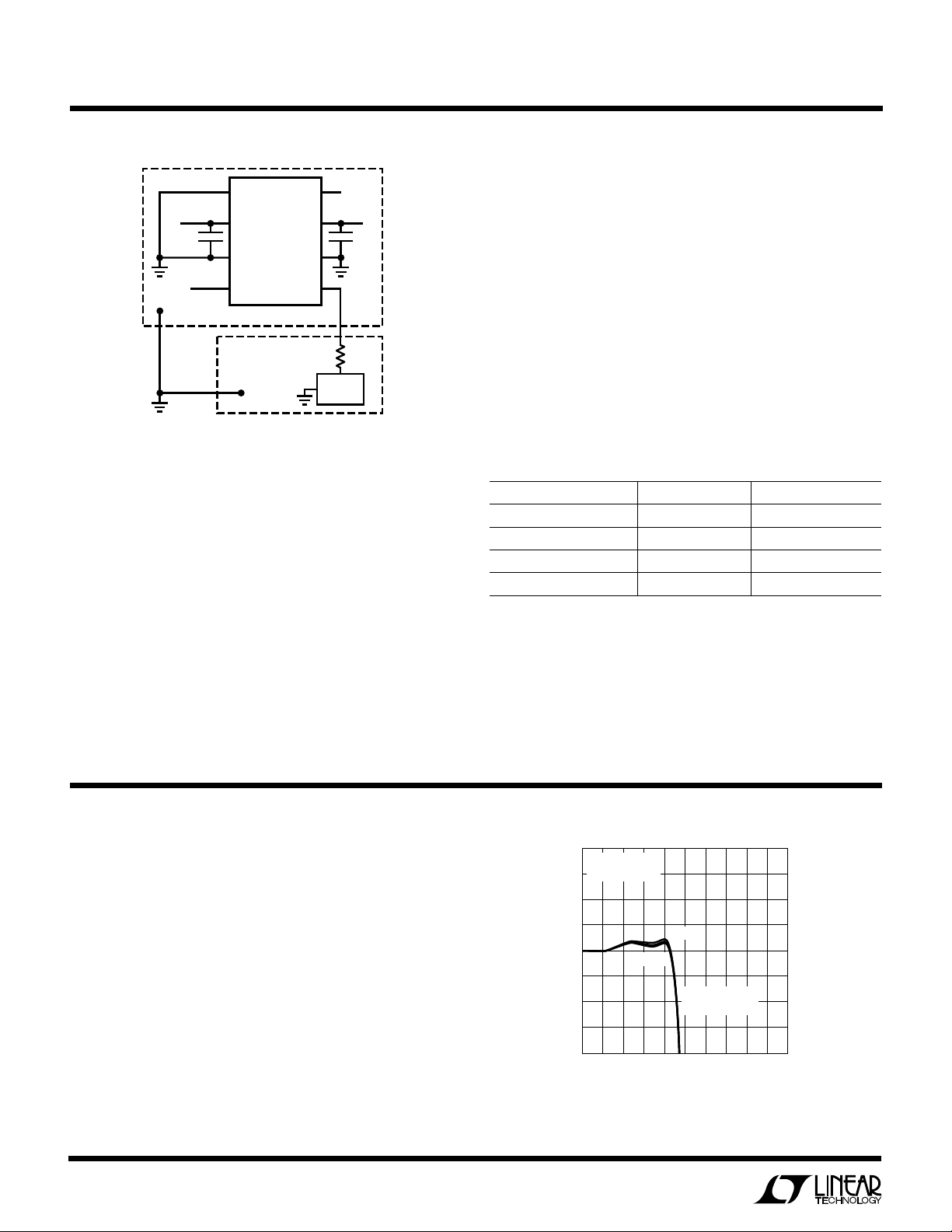
if used to bias other ICs. Figure 2 shows the connections
for single supply operation.
1
AGND
+
2
V
11.325k 8.775k
3
NC
LTC1069-6
4
V
IN
Figure 1. Internal Biasing of the Analog Ground (Pin 1)
V
OUT
V
NC
CLK
1069-6 F01
8
–
7
6
5
V+, V– (Pins 2, 7): Power Supply Pins. The V+ (Pin 2) and
the V– (Pin 7, if used) should be bypassed with a 0.1µF
capacitor to an adequate analog ground. The filter’s power
supplies should be isolated from other digital or high
voltage analog supplies. A low noise linear supply is
recommended. Switching power supplies will lower the
signal-to-noise ratio of the filter. Unlike previous monolithic filters, the power supplies can be applied in any
order, that is, the positive supply can be applied before the
negative supply and vice versa. Figure 3 shows the connection for dual supply operation.
1
0.47µF
0.1µF
V
IN
STAR
SYSTEM
GROUND
AGND
2
+
+
V
V
LTC1069-6
3
NC
4
V
IN
ANALOG GROUND PLANE
DIGITAL
GROUND
PLANE
Figure 2. Connections for Single Supply Operation
V
OUT
NC
CLK
–
V
8
V
7
6
5
CLOCK
SOURCE
OUT
1k
1069-6 F02
5

LTC1069-6
UUU
PIN FUNCTIONS
1
AGND
2
+
V
0.1µF 0.1µF
V
IN
STAR
SYSTEM
GROUND
+
V
LTC1069-6
3
NC
4
V
IN
ANALOG GROUND PLANE
DIGITAL
GROUND
PLANE
8
V
OUT
NC
CLK
V
–
SOURCE
V
7
6
5
CLOCK
OUT
1k
1069-6 F03
–
V
Figure 3. Connections for Dual Supply Operation
NC (Pins 3, 6): No Connection. Pins 3 and 6 are not
connected to any internal circuitry; they should be tied to
ground.
VIN (Pin 4): Filter Input Pin. The Filter Input pin is internally
connected to the inverting input of an op amp through a
50k resistor.
only. Table 1 shows the clock’s low and high level threshold value for a dual or single supply operation. A pulse
generator can be used as a clock source provided the high
level ON time is greater than 0.42µs (VS = ±5V). Sine
waves less than 100kHz are not recommended for clock
frequencies because, excessive slow clock rise or fall
times generate internal clock jitter. The maximum clock
rise or fall time is 1µ s. The clock signal should be routed
from the right side of the IC package to avoid coupling into
any input or output analog signal path. A 1k resistor
between the clock source and the Clock Input (Pin 5) will
slow down the rise and fall times of the clock to further
reduce charge coupling (Figure 1).
Table 1. Clock Source High and Low Thresholds
POWER SUPPLY HIGH LEVEL LOW LEVEL
Dual Supply = ±5V 1.5V 0.5V
Single Supply = 10V 6.5V 5.5V
Single Supply = 5V 1.5V 0.5V
Single Supply = 3.3V 1.2V 0.5V
CLK (Pin 5): Clock Input Pin. Any TTL or CMOS clock
source with a square wave output and 50% duty cycle
(±10%) is an adequate clock source for the device. The
power supply for the clock source should not necessarily
be the filter’s power supply. The analog ground of the filter
should be connected to the clock’s ground at a single point
U
WUU
APPLICATIONS INFORMATION
Temperature Behavior
The power supply current of the LTC1069-6 has a positive
temperature coefficient. The GBW product of its internal
op amps is nearly constant and the speed of the device
does not degrade at high temperatures. Figures 4a, 4b and
4c show the behavior of the passband of the device for
various supplies and temperatures. The filter has a passband behavior which is temperature independent.
V
(Pin 8): Filter Output Pin. Pin 8 is the output of the
OUT
filter, and it can source 8mA or sink 1mA. The total
harmonic distortion of the filter will degrade when driving
coaxial cables or loads less than 20k without an output
buffer.
2
VS = SINGLE 3V
= 0.5V
V
IN
RMS
1
85°C
0
GAIN (dB)
–1
–2
1
–40°C
f
= 500kHz
CLK
= 10kHz
f
CUTOFF
5
7
319
FREQUENCY (kHz)
13
15
17
9
11
21
1069-6 F04a
Figure 4a
6

LTC1069-6
U
WUU
APPLICATIONS INFORMATION
2
VS = SINGLE 5V
= 1V
V
IN
RMS
1
0
GAIN (dB)
–1
–2
1
2
1
0
GAIN (dB)
–1
f
= 750kHz
CLK
f
CUTOFF
5
7
319
9
FREQUENCY (kHz)
Figure 4b
VS = ±5V
= 1.5V
V
IN
RMS
f
= 1MHz
CLK
= 20kHz
f
CUTOFF
–40°C
= 15kHz
13
11
–40°C
85°C
85°C
15
17
21
1069-6 F04a
quency contents much higher than the applied clock; their
amplitude strongly depends on scope probing techniques
as well as grounding and power supply bypassing. The
clock feedthrough can be reduced by adding a single RC
lowpass filter at the Output (Pin 8).
Wideband Noise
The wideband noise of the filter is the total RMS value of
the device’s noise spectral density and determines the
operating signal-to-noise ratio. The frequency contents of
the wideband noise lie within the filter’s passband. The
wideband noise cannot be reduced by adding post filtering. The total wideband noise is nearly independent of the
clock frequency and depends slightly on the power supply
voltage (see Table 3). The clock feedthrough specifications are not part of the wideband noise.
Table 3. Wideband Noise
V
S
3.3V 118µV
5V 123µV
±5V 127µV
WIDEBAND NOISE
RMS
RMS
RMS
–2
7
1
10
428
FREQUENCY (kHz)
19
22
25
13
16
31
1069-6 F04c
Figure 4c
Clock Feedthrough
The clock feedthrough is defined as the RMS value of the
clock frequency and its harmonics that are present at the
filter’s Output (Pin 8). The clock feedthrough is tested with
the Input (Pin 4) shorted to AGND (Pin 1) and depends on
PC board layout and on the value of the power supplies.
With proper layout techniques the values of the clock
feedthrough are shown in Table 2.
Table 2. Clock Feedthrough
V
S
3.3V 100µV
5V 170µV
10V 350µV
CLOCK FEEDTHROUGH
RMS
RMS
RMS
Any parasitic switching transients during the rising and
falling edges of the incoming clock are not part of the clock
feedthrough specifications. Switching transients have fre-
Aliasing
Aliasing is an inherent phenomenon of sampled data
systems and occurs for input frequencies approaching the
sampling frequency. The internal sampling frequency of
the LTC1069-6 is 100 times its cutoff frequency. For
instance, if a 98.5kHz, 100mV
signal is applied at the
RMS
input of an LTC1069-6 operating with a 50kHz clock, a
1.5kHz, 484µV
alias signal will appear at the filter
RMS
output. Table 4 shows details.
Table 4. Aliasing (f
INPUT FREQUENCY OUTPUT LEVEL OUTPUT FREQUENCY
= 1V
(V
IN
RMS
(kHz) (dB) (kHz)
f
= 50:1, f
CLK/fC
96 (or 104) –78.3 4.0
97 (or 103) –70.4 3.0
98 (or 102) –80.6 2.0
98.5 (or 101.5) –46.3 1.5
99 (or 101) –2.8 1.0
99.5 (or 100.5) –1.38 0.5
CUTOFF
= 50kHz)
CLK
) (Relative to Input) (Aliased Frequency)
= 1kHz
Information furnished by Linear Technology Corporation is believed to be accurate and reliable.
However, no responsibility is assumed for its use. Linear Technology Corporation makes no representation that the interconnection of its circuits as described herein will not infringe on existing patent rights.
7

LTC1069-6
TYPICAL APPLICATIONS
U
ON
Single 5V Operation with Power Shutdown
5V
SHUTDOWN
1
AGND
2
0.47µF
0.1µF
+
V
LTC1069-6
3
NC
4
V
V
IN
IN
Single 3V Supply Voice Band Lowpass Filter with Rail-to-Rail Input and Output
10k
270pF
Single 3V Supply Operation with Output Buffer
3.3V
+
1/2 LT1366
–
8
4
0.1µF
1069-6 TA04
7
V
OUT
8
OUT
CLK
V
NC
–
2
3
40.2k
7
6
5
V
OUT
f
CLK ≤
750kHz
–
1/2 LT1366
+
4
1µF
0.1µF
1069-6 TA03
3V
1
3.3V
0V
5
6
1
V
8
7
6
5
IN
170kHz
2
3
4
AGND
+
V
LTC1069-6
NC
V
IN
0.47µF
0.1µF
5V
0V
1
2
3
4
AGND
+
V
LTC1069-6
NC
V
IN
V
OUT
–
V
NC
CLK
V
OUT
V
NC
CLK
5
+
1/2 LT1366
6
–
40.2k
8
7
–
6
f
5
CLK
500kHz
3V
0.1µF
8
7
10k
1069-6 TA05
V
U
PACKAGE DESCRIPTION
0.010 – 0.020
(0.254 – 0.508)
0.008 – 0.010
(0.203 – 0.254)
*
DIMENSION DOES NOT INCLUDE MOLD FLASH. MOLD FLASH
SHALL NOT EXCEED 0.006" (0.152mm) PER SIDE
**
DIMENSION DOES NOT INCLUDE INTERLEAD FLASH. INTERLEAD
FLASH SHALL NOT EXCEED 0.010" (0.254mm) PER SIDE
× 45°
0.016 – 0.050
0.406 – 1.270
Dimensions in inches (millimeters) unless otherwise noted.
S8 Package
8-Lead Plastic Small Outline (Narrow 0.150)
(LTC DWG # 05-08-1610)
8
1
0°– 8° TYP
0.053 – 0.069
(1.346 – 1.752)
0.014 – 0.019
(0.355 – 0.483)
0.004 – 0.010
(0.101 – 0.254)
0.050
(1.270)
BSC
0.228 – 0.244
(5.791 – 6.197)
0.189 – 0.197*
(4.801 – 5.004)
7
6
3
2
5
0.150 – 0.157**
(3.810 – 3.988)
SO8 0695
4
RELATED PARTS
PART NUMBER DESCRIPTON COMMENTS
LTC1068 Very Low Noise, High Accuracy, Quad Universal Filter Building Block User-Configurable, SSOP Package
LTC1069-1 Low Power, Progressive Elliptic LPF f
LTC1164-5 Low Power 8th Order Butterworth LPF f
LTC1164-6 Low Power 8th Order Elliptic LPF f
LTC1164-7 Low Power 8th Order Linear Phase LPF f
Ratio 100:1, 8-Pin SO Package
CLK/fC
Ratio 100:1 and 50:1
CLK/fC
Ratio 100:1 and 50:1
CLK/fC
Ratio 100:1 and 50:1
CLK/fC
8
Linear Technology Corporation
1630 McCarthy Blvd., Milpitas, CA 95035-7417
(408) 432-1900
●
FAX
: (408) 434-0507
●
TELEX
: 499-3977
LT/GP 1196 7K • PRINTED IN USA
LINEAR TECHNOLOGY CORPORATION 1996
 Loading...