

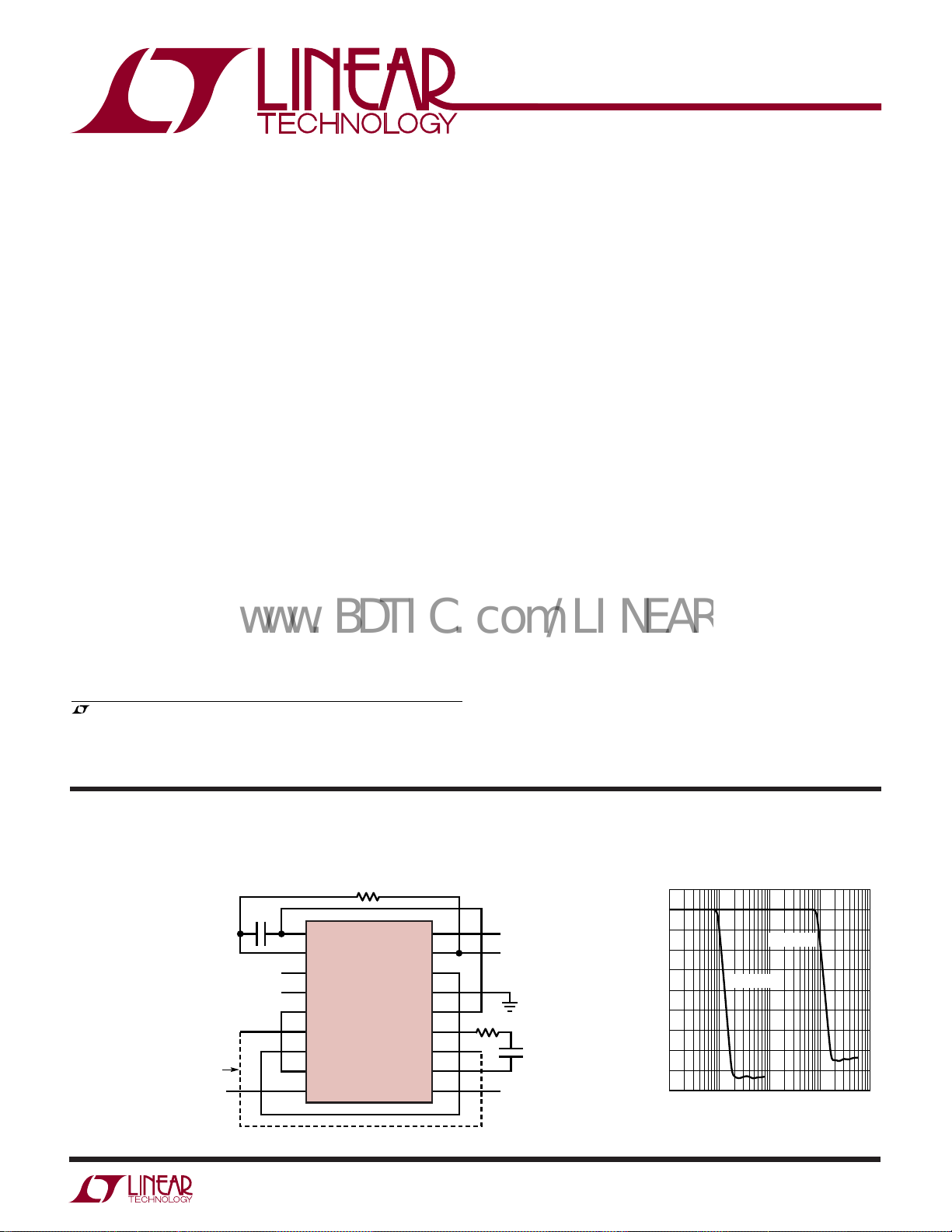
FREQUENCY (Hz)
100 10k 100k 1M
1066-1 TA02
1k
GAIN (dB)
10
0
–10
–20
–30
–40
–50
–60
–70
–80
–90
fC = 800Hz
fC = 80kHz
FEATURES
www.BDTIC.com/LINEAR
■
DC Gain Linearity: 14 Bits
■
Maximum DC Offset: ± 1.5mV
■
DC Offset TempCo: 7µV/°C
■
Device Fully Tested at f
■
Maximum Cutoff Frequency: 120kHz (VS = ± 8V)
■
Drives 1kΩ Load with 0.02% THD or Better
■
Signal-to-Noise Ratio: 90dB
■
Input Impedance: 500MΩ
■
Selectable Elliptic or Linear Phase Response
■
Operates from Single 5V up to ±8V Power Supplies
■
Available in an 18-Pin SO Wide Package
CUTOFF
= 80kHz
U
APPLICATIO S
■
Instrumentation
■
Data Acquisition Systems
■
Anti-Aliasing Filters
■
Smoothing Filters
■
Audio Signal Processing
, LTC and LT are registered trademarks of Linear Technology Corporation.
All other trademarks are the property of their respective owners.
LTC1066-1
14-Bit DC Accurate
Clock-Tunable, 8th Order Elliptic
or Linear Phase Lowpass Filter
U
DESCRIPTIO
The LTC®1066-1 is an 8th order elliptic lowpass filter
which simultaneously provides clock-tunability and DC
accuracy. The unique and proprietary architecture of the
filter allows 14 bits of DC gain linearity and a maximum of
1.5mV DC offset. An external RC is required for DC
accurate operation. With ±7.5V supplies, a 20k resistor
and a 1µF capacitor, the cutoff frequency can be tuned
from 800Hz to 100kHz. A clock-tunable 10Hz to 100kHz
operation can also be achieved (see Typical Application
section).
The filter does not require any external active components
such as input/output buffers. The input/output impedance
is 500MΩ/0.1Ω and the output of the filter can source or
sink 40mA. When pin 8 is connected to V
cutoff frequency ratio is 50:1 and the input signal is
sampled twice per clock cycle to lower the risk of aliasing.
For frequencies up to 0.75f
± 0.15dB. The gain at f
CUTOFF
, the passband ripple is
CUTOFF
is –1dB and the filter’s
stopband attenuation is 80dB at 2.3f
operation is also available with a clock-to-cutoff frequency
ratio of 100:1 when pin 8 is connected to ground.
+
CUTOFF
, the clock-to-
. Linear phase
U
TYPICAL APPLICATIO
Clock-Tunable, DC Accurate, 800Hz to 80kHz Elliptic Lowpass Filter
20k
1µF
1
OUT A
2
–IN A
3
SHORT CONNECTION UNDER
BYPASS THE POWER SUPPLIES
IC AND SHIELDED BY A
GROUND PLANE
WITH 0.1µF DISC CERAMIC
40kHz ≤ f
CLK
≤ 4MHz
V
–7.5V
7.5V
+IN A
IN
4
–
V
5
6
7
8
9
LTC1066-1
+
V
CONNECT 1
FILTER
OUT
50/100
CLK
FILTER
CONNECT 2
OUT B
+IN B
GND
COMP 2
COMP 1
18
+
V
17
16
15
14
IN
13
12
11
10
–
V
The LTC1066-1 is available in an 18-pin SO Wide package.
Amplitude Response
7.5V
V
;
OUT
=
V
OS(OUT)
2.5mV
MAX
30k
15pF
–7.5V
1066-1 TA01
10661fa
1
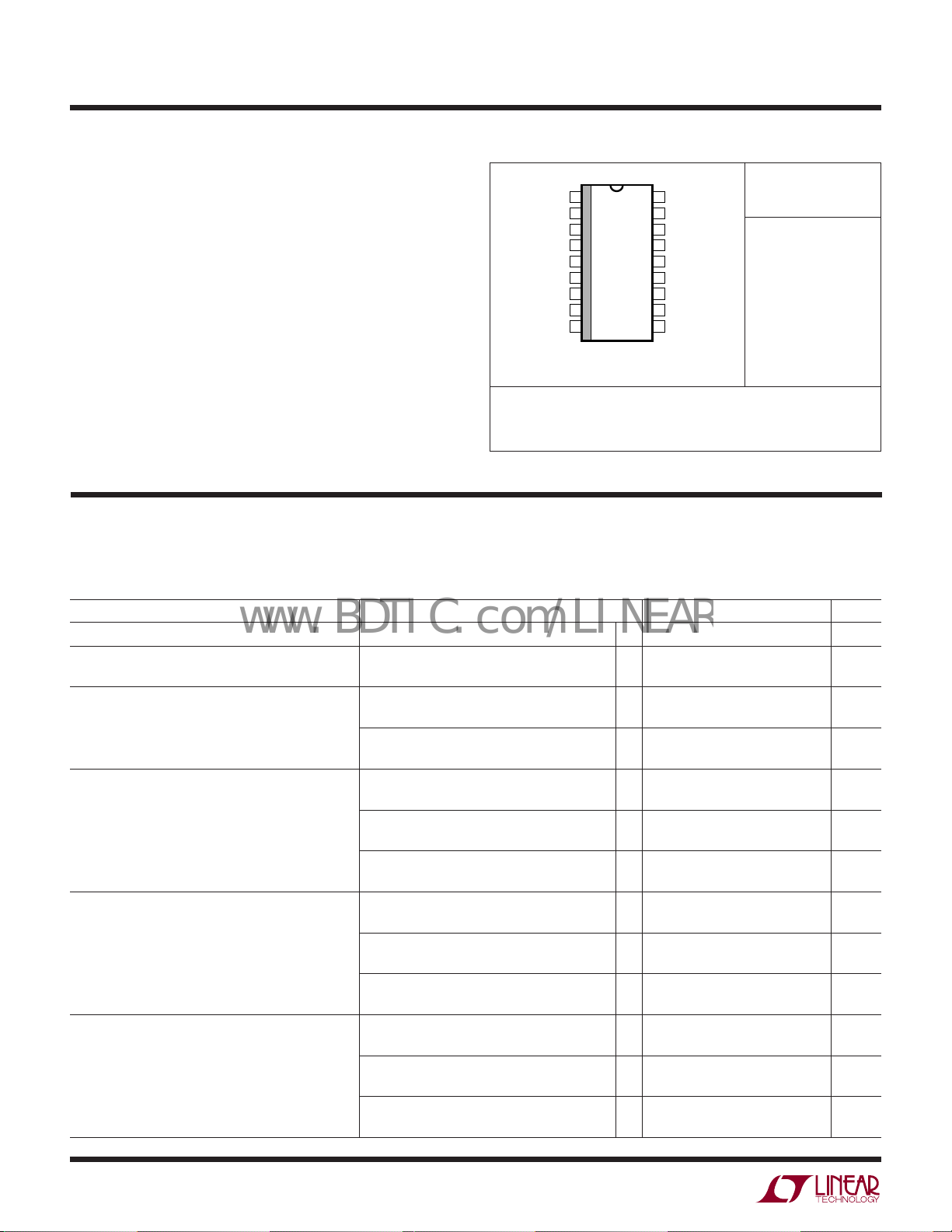
LTC1066-1
TOP VIEW
SW PACKAGE
18-LEAD PLASTIC SO WIDE
T
JMAX
= 110°C, θJA = 75°C/W
1
2
3
4
5
6
7
8
9
18
17
16
15
14
13
12
11
10
OUT A
–IN A
+IN A
V
–
V
+
CONNECT 1
FILTER
OUT
50/100
CLK
V
+
OUT B
+IN B
GND
FILTER
IN
COMP 2
CONNECT 2
COMP 1
V
–
www.BDTIC.com/LINEAR
WW
W
ABSOLUTE AXI U RATI GS
U
PACKAGE
/
O
RDER I FOR ATIO
WU
(Note 1)
Total Supply Voltage (V+ to V–) .......................... 16.5V
ORDER PART
NUMBER
Power Dissipation............................................. 700mW
Burn-In Voltage ................................................... 16.5V
LTC1066-1CSW
Voltage at Any Input ..... (V– – 0.3V) ≤ VIN ≤ (V+ + 0.3V)
Maximum Clock Frequency
V
= ± 8V ....................................................... 6.1MHz
S
= ± 7.5V .................................................... 5.4MHz
V
S
V
= ± 5V ....................................................... 4.1MHz
S
VS = Single 5V ............................................... 1.8MHz
Operating Temperature Range* .................. 0°C to 70°C
Storage Temperature Range ................. –65°C to 150°C
Lead Temperature (Soldering, 10 sec).................. 300°C
* For an extended operating temperature range contact LTC Marketing
for details.
ELECTRICAL CHARACTERISTICS
The ● denotes the specifications which apply over the full operating temperature range, otherwise specifications are at VS = ± 7.5V,
RL = 1k, TA = 25°C, f
measurements are referenced to passband gain.
signal level is TTL or CMOS (maximum clock rise or fall time ≤ 1µs) unless otherwise specified. All AC gain
CLK
(See Test Circuit)
Order Options Tape and Reel: Add #TR
Lead Free: Add #PBF Lead Free Tape and Reel: Add #TRPBF
Lead Free Part Marking: http://www.linear.com/leadfree/
Consult LTC Marketing for parts specified with wider operating temperature ranges.
U
PARAMETER CONDITIONS MIN TYP MAX UNITS
Passband Gain (0.01f
Passband Ripple (0.01f
for f
CLK/fCUTOFF
Gain at 0.50f
Gain at 0.75f
Gain at 1.00f
Gain at 2.00f
2
CUTOFF
CUTOFF
CUTOFF
CUTOFF
= 50:1
for f
for f
for f
for f
CUTOFF
CUTOFF
CLK/fCUTOFF
CLK/fCUTOFF
CLK/fCUTOFF
CLK/fCUTOFF
to 0.25f
CUTOFF
to 0.75f
CUTOFF
= 50:1 f
= 50:1 f
= 50:1 f
= 50:1 f
)f
)f
= 400kHz, f
CLK
≤ 50kHz (See Note on Test Circuit) ± 0.15 dB
CUTOFF
= 400kHz, f
CLK
= 2MHz, f
f
CLK
= 400kHz, f
CLK
= 2MHz, f
f
CLK
= 4MHz, f
f
CLK
= 400kHz, f
CLK
= 2MHz, f
f
CLK
= 4MHz, f
f
CLK
= 400kHz, f
CLK
= 2MHz, f
f
CLK
= 4MHz, f
f
CLK
TEST
TEST
TEST
TEST
TEST
TEST
TEST
TEST
TEST
TEST
TEST
TEST
= 2kHz ● – 0.18 0.16 0.36 dB
= 4kHz – 0.09 0.02 0.09 dB
● – 0.14 0.05 0.14 dB
= 20kHz – 0.16 – 0.05 0.02 dB
● – 0.22 – 0.10 0.02 dB
= 6kHz – 0.18 – 0.05 0.05 dB
● – 0.22 – 0.10 0.05 dB
= 30kHz – 0.36 – 0.20 0.05 dB
● – 0.45 – 0.30 0.05 dB
= 60kHz – 0.65 – 0.30 0.25 dB
● – 0.85 – 0.40 0.75 dB
= 8kHz – 1.50 – 1.10 – 0.05 dB
● – 1.80 – 1.20 – 0.05 dB
= 40kHz – 2.10 – 1.60 – 1.20 dB
● – 2.30 – 1.60 – 1.20 dB
= 80kHz – 2.20 – 1.60 – 0.05 dB
● – 2.50 – 1.60 0.25 dB
= 16kHz – 56 – 58 –64 dB
● –54 –57 –64 dB
= 80kHz – 53 – 56 –62 dB
● –51 –55 –62 dB
= 160kHz – 50 – 52 –60 dB
● –48 –51 –60 dB
10661fa
LTC1066-1
www.BDTIC.com/LINEAR
LECTRICAL C CHARA TERIST
E
The ● denotes the specifications which apply over the full operating temperature range, otherwise specifications are at VS = ± 7.5V,
= 1k, TA = 25°C, f
R
L
measurements are referenced to passband gain.
PARAMETER CONDITIONS MIN TYP MAX UNITS
Gain at f
Gain at f
Gain at 70kHz for VS = ±5V, f
Linear Phase Response Phase at 0.25f
f
CLK/fCUTOFF
Pin 8 at GND Gain at 0.25f
Input Bias Current V
Input Offset Current V
Input Offset Current TempCo ±2.375V ≤ VS ≤ ±7.5V 40 pA/°C
Output Voltage Offset TempCo ±2.375V ≤ VS ≤ ±7.5V 7 µV/°C
Output Offset Voltage V
Common Mode Rejection VS = ±7.5V 90 96 dB
Power Supply Rejection V
Input Voltage Range and Output Voltage Swing V
Output Short-Circuit Current ± 2.375V ≤ VS ≤ ±7.5V ± 20 mA
Power Supply Current (Note 2) VS = ±2.375V 14 16 mA
Power Supply Range ± 2.375 ±8V
for f
CUTOFF
for VS = ±2.375V, f
CUTOFF
= 100:1, ● –48.0 –50.0 –52.0 Deg
signal level is TTL or CMOS (maximum clock rise or fall time ≤ 1µs) unless otherwise specified. All AC gain
CLK
= 20kHz, VS = ±7.5V f
CLK
CLK/fCUTOFF
CLK/fCUTOFF
Phase at 0.50f
Gain at 0.50f
Phase at 0.75f
Gain at 0.75f
Phase at f
Gain at f
CUTOFF
= 50:1 f
= 50:1 f
CUTOFF
CUTOFF
CUTOFF
CUTOFF
CUTOFF
CUTOFF
CUTOFF
ICS
(See Test Circuit)
CLK/fCUTOFF
CLK
CLK
f
CLK
f
CLK
f
CLK
f
CLK
f
CLK
f
CLK
f
CLK
f
CLK
= ±2.375V 60 nA
S
= ±2.375V ● ± 10 ± 40 nA
S
VS ≥ ±5V (Note 3) ● ± 10 ± 45 nA
= ±2.375V, f
S
≥ ±5V ±0.5 mV
V
S
(Note 3) ● ±1.0 ±1.5 mV
= 50:1, f
= 1MHz, f
= 4MHz, f
= 400kHz, f
= 400kHz, f
= 400kHz, f
= 400kHz, f
= 400kHz, f
= 400kHz, f
= 400kHz, f
= 400kHz, f
TEST
TEST
TEST
TEST
TEST
TEST
TEST
TEST
TEST
TEST
CLK
= 400Hz ● – 1.75 –1.25 –0.50 dB
TEST
= 20kHz ● –1.75 –0.70 0.10 dB
= 70kHz ● 1.00 1.40 dB
= 1kHz –48.5 –50.0 –51.5 Deg
= 1kHz ● –0.65 –0.25 0.25 dB
= 2kHz –97.5 –99.5 –101.5 Deg
● –97.0 –99.5 –102.0 Deg
= 2kHz ● –0.75 –0.50 –0.10 dB
= 3kHz – 148.0 –150.5 –152.5 Deg
● – 147.5 – 150.5 –153.0 Deg
= 3kHz ● –1.40 –1.00 –0.60 dB
= 4kHz – 208.0 –210.0 –212.5 Deg
● – 207.5 – 210.0 –213.0 Deg
= 4kHz ● –2.10 –1.80 –1.60 dB
● 70 135 nA
= 400kHz ±0.5 mV
● ±1.0 ±1.5 mV
VCM = –5V to 5V ● 84 90 dB
= ±2.5V to ±7.5V 80 84 dB
S
= ±2.375V, RL = 1k ±1.2 ± 1.4 V
S
= ± 5V, RL = 1k ±3.4 ± 3.6 V
V
S
= ±7.5V, RL = 1k ±5.4 ± 5.8 V
V
S
= ±5V 22 26 mA
V
S
= ±7.5V 25 30 mA
V
S
● 78 82 dB
● ± 1.1 V
● ± 3.2 V
● ± 5.0 V
● 16 19 mA
● 23 29 mA
● 26 33 mA
Note 1: Absolute Maximum Ratings are those values beyond which the life
of a device may be impaired.
Note 2: The maximum current over temperature is at 0°C. At 70°C the
maximum current is less than its maximum value at 25°C.
Note 3: Guaranteed by design and test correlation.
10661fa
3
LTC1066-1
www.BDTIC.com/LINEAR
LPER
F
O
R
ATYPICA
UW
CCHARA TERIST
E
C
ICS
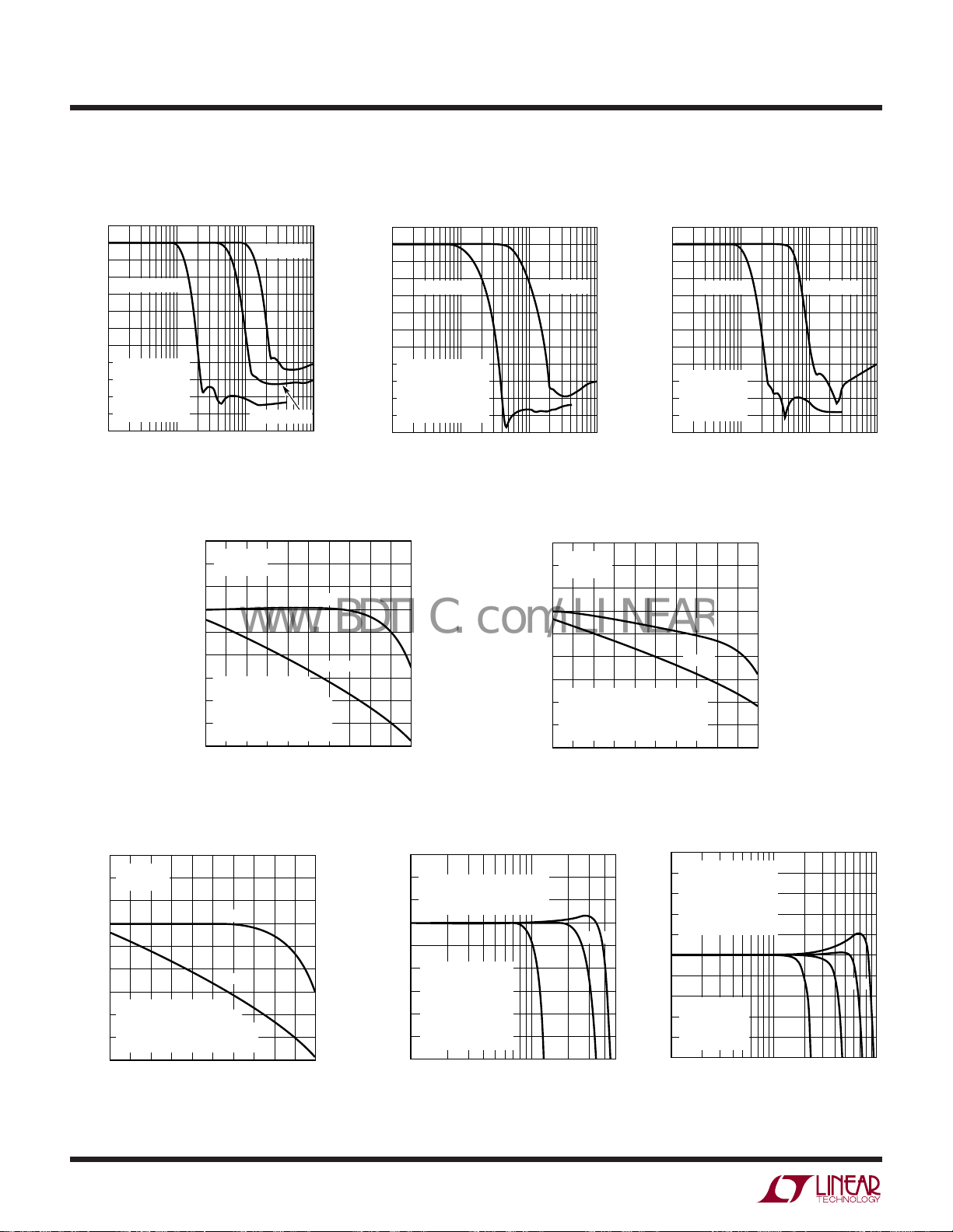
Gain vs Frequency
VS = ± 7.5V, f
10
0
–10
–20
f
= 500kHz
CLK
–30
–40
–50
–60
GAIN (dB)
–70
VS = ±7.5V
= 25°C
T
A
–80
–90
–100
–110
= 50:1
f
CLK/fC
COMPENSATION
= 30k, 15pF
1k
= 50:1
CLK/fC
f
= 5MHz
CLK
f
= 2.5MHz
CLK
10k 100k 1M
FREQUENCY (Hz)
1066-1 G01
Passband Gain and Phase
vs Frequency
3
VS = ±7.5V
2
= 25°C
T
A
1
0
–1
–2
GAIN (dB)
–3
ELLIPTIC RESPONSE
= 20kHz, f
f
C
–4
f
CLK/fC
RF = 20k, CF = 1µF
–5
(SEE BLOCK DIAGRAM)
–6
2
4
= 1MHz
CLK
= 50:1, PIN 8 AT V
810141822
6
12
FREQUENCY (kHz)
GAIN
PHASE
+
Gain vs Frequency
V
S
10
0
–10
–20
–30
–40
–50
–60
GAIN (dB)
–70
VS = ±7.5V
T
–80
f
CLK/fC
–90
NO COMPENSATION
–100
PIN 8 TO AGND
–110
1k
16
20
10666-1 G04
= ± 7.5V, f
f
CLK
= 25°C
A
180
120
60
0
–60
–120
–180
–240
–300
–360
CLK/fC
= 1MHz
= 100:1
10k 100k 1M
FREQUENCY (Hz)
PHASE (DEG)
= 100:1
f
CLK
3
2
1
0
–1
–2
GAIN (dB)
–3
–4
–5
–6
Gain vs Frequency
VS = ± 7.5V, f
10
0
–10
= 5MHz
1066-1 G02
–20
–30
–40
–50
–60
GAIN (dB)
–70
–80
–90
–100
–110
1k
VS = ±7.5V
= 25°C
T
A
f
CLK/fC
PIN 8 TO V
Passband Gain and Phase
vs Frequency
VS = ±7.5V
= 25°C
T
A
GAIN
PHASE
LINEAR PHASE RESPONSE
= 20kHz, f
f
C
PIN 8 AT GND, R
(SEE BLOCK DIAGRAM)
6
2
4
= 100:1
CLK/fC
= 20k, CF = 1µF
F
810141822
FREQUENCY (kHz)
16
12
= 100:1
CLK/fC
f
= 1MHz
CLK
= 100:1
–
10k 100k 1M
FREQUENCY (Hz)
180
120
60
0
PHASE (DEG)
–60
–120
–180
–240
–300
–360
20
10666-1 G05
f
CLK
= 5MHz
1066-1 G03
Passband Gain and Phase
vs Frequency
3
VS = ±7.5V
2
= 25°C
T
A
1
0
–1
–2
GAIN (dB)
–3
ELLIPTIC RESPONSE
–4
= 20kHz, f
f
C
PIN 8 AT V
–5
(SEE BLOCK DIAGRAM)
–6
6
2
4
= 100:1
CLK/fC
–
, RF = 20k, CF = 1µF
810141822
FREQUENCY (kHz)
12
GAIN
PHASE
180
120
60
0
PHASE (DEG)
–60
–120
–180
–240
–300
20
10666-1 G06
–360
16
Passband Gain vs Frequency
and f
CLK
3
2
A. f
= 1MHz (GND = 2.5V)
CLK
= 1.4MHz (GND = 2V)
B. f
CLK
1
0
–1
–2
GAIN (dB)
–3
–4
–5
–6
= 1.8MHz (GND = 2V)
C. f
CLK
VS = SINGLE 5V
= 70°C
T
A
= 50:1
f
CLK/fC
= 20k, CF = 1µF
R
F
RC COMPENSATION
= 15pF IN SERIES
WITH 30kΩ
1
4
A
10 50
FREQUENCY (kHz)
B
1066-1 G07
Passband Gain vs Frequency
and f
CLK
5
VS = ±5V, TA = 70°C
4
3
2
C
1
0
GAIN (dB)
–1
–2
–3
–4
–5
= 50:1
f
CLK/fC
= 20k, CF = 1µF
R
F
RC COMPENSATION
=15pF IN SERIES
WITH 30kΩ
A. f
= 1MHz
CLK
= 2MHz
B. f
CLK
= 3MHz
C. f
CLK
= 4MHz
D. f
CLK
1
FREQUENCY (kHz)
B
D
A
10 100
C
1066-1 G08
10661fa
FREQUENCY (kHz)
1
–90
–80
–70
–60
–50
10
1066-1 G17
–85
–75
–65
–55
–45
VS = SINGLE 5V
V
IN
= 0.5V
RMS
TA = 25°C
f
CLK
= 1MHz
f
CLK/fC
= 50:1
(5 REPRESENTATIVE
UNITS)
–40
20
V
IN
THD + NOISE
()
(dB)20 log
FREQUENCY (kHz)
11050
1066-1 G14
–90
–80
–50
–70
–65
–55
–40
–45
–60
–75
–85
VS = ±7.5V
V
IN
= 1V
RMS
TA = 25°C
f
CLK
= 2.5MHz
f
CLK/fC
= 50:1
(5 REPRESENTATIVE
UNITS)
V
IN
THD + NOISE
()
(dB)20 log
LPER
www.BDTIC.com/LINEAR
LTC1066-1
UW
R
F
O
ATYPICA
CCHARA TERIST
E
C
ICS
Passband Gain vs Frequency Group Delay vs Frequency
5
VS = ±5V, TA = 70°C
4
3
2
1
0
GAIN (dB)
–1
–2
–3
–4
–5
= 50:1
f
CLK/fC
= 20k, CF = 1µF
R
F
RC COMPENSATION
=15pF IN SERIES
WITH 30kΩ
A. f
= 1MHz
CLK
= 2MHz
B. f
CLK
= 3MHz
C. f
CLK
= 4MHz
D. f
CLK
1
A
10 100
FREQUENCY (kHz)
B
D
C
1066-1 G08
THD + Noise vs Input Voltage
–40
TA = 25°C
–45
= 1kHz
f
IN
= 1MHz
f
CLK
–50
(dB)20 log
–55
–60
IN
–65
V
THD + NOISE
–70
()
–75
–80
–85
–90
0.1 1 5
f
CLK/fC
= 50:1
VS = ±7.5V
INPUT VOLTAGE (V
VS = ±5V
)
RMS
1066-1 G12
80
A. f
= 50:1 (PIN 8 TO V+)
CLK/fC
= 100:1 (PIN 8 TO V–)
B. f
CLK/fC
70
C. LINEAR PHASE REPONSE
= 100:1 (PIN 8 TO GND)
f
CLK/fC
60
VS = ±5V
= 25°C
T
A
50
= 20kHz
f
C
40
GROUP DELAY (µs)
30
20
41281620
2
6101418
FREQUENCY (kHz)
THD + Noise vs Input Voltage THD + Noise vs Frequency
–40
fIN = 1kHz
–45
= SINGLE 5V
V
S
= 1MHz
f
–50
CLK
= 50:1
f
(dB)20 log
THD + NOISE
CLK/fC
–55
= 25°C
T
A
–60
IN
–65
V
–70
()
–75
–80
–85
–90
0.1
GND PIN 15 AT 2V
INPUT VOLTAGE (V
1066-1 G10
GND PIN 15 AT 2.5V
1
)
RMS
1066-1 G13
Phase Matching vs Frequency
1.25
PHASE DIFFERENCE BETWEEN
ANY TWO UNITS (SAMPLE OF
A
B
C
22
2
50 REPRESENTATIVE UNITS)
1.00
≥ ±5V, TA = 25°C
V
S
≤ 2.5MHz
f
CLK
0.75
0.50
PHASE DIFFERENCE (±DEG)
0.25
0
0.2
0.4
FREQUENCY (f
A
B
A. ELLIPTIC RESPONSE
= 50:1 (PIN 8 to V+)
f
CLK/fC
B. LINEAR PHASE RESPONSE
= 100:1 (PIN8 TO GND)
f
CLK/fC
0.6
CUTOFF
0.8
/FREQUENCY)
1.0
1066-1 G11
THD + Noise vs Frequency THD + Noise vs Frequency THD + Noise vs Frequency
–40
VS = ±7.5V
–45
–50
(dB)20 log
–55
–60
IN
–65
V
–70
THD + NOISE
()
–75
–80
–85
–90
= 1V
V
IN
RMS
TA = 25°C
= 2.5MHz
f
CLK
= 50:1
f
CLK/fC
C
B
A
1066-1 G15
A. RL = ∞, CL = 100pF
= 1k, CL = 100pF
B. R
L
= 200Ω, CL = 100pF
C. R
L
11050
FREQUENCY (kHz)
–40
VS = ±5V
–45
–50
(dB)20 log
–55
–60
IN
–65
V
–70
THD + NOISE
()
–75
–80
–85
–90
= 1V
V
IN
RMS
TA = 25°C
= 1MHz
f
CLK
= 50:1
f
CLK/fC
(5 REPRESENTATIVE
UNITS)
1
FREQUENCY (kHz)
10
20
1066-1 G16
10661fa
5
LTC1066-1
www.BDTIC.com/LINEAR
LPER
Power Supply Current vs
Power Supply Voltage
30
27
24
21
18
15
12
9
6
POWER SUPPLY CURRENT (mA)
3
0
2 6 10 14 18
4
0
TOTAL POWER SUPPLY VOLTAGE (V)
8
F
O
12
R
UW
ATYPICA
0°C
25°C
70°C
16
1066-1 G18
CCHARA TERIST
E
C
Transient Response
1V/DIV
ELLIPTIC RESPONSE (PIN 8 TO V
f
= 1kHz, f
20
IN
CUTOFF
100µs/DIV
= 10kHz
ICS
+
)
1066-1 G19
Transient Response
1V/DIV
CUTOFF
100µs/DIV
= 10kHz
LINEAR PHASE (PIN 8 TO GND)
f
= 1kHz, f
IN
1066-1 G20
Table 1. Elliptic Response, fC = 10kHz, f
CLK/fCUTOFF
= 50:1,
VS = ± 7.5V, RF = 20k, CF = 1µF, No RC Compensation,
TA = 25°C
FREQUENCY GAIN PHASE GROUP DELAY
(kHz) (dB) (DEG) (µs)
2.000 0.117 –50.09 70.52
3.000 0.118 –75.75 72.04
4.000 0.116 –101.96 74.32
5.000 0.112 –129.25 77.59
6.000 0.104 –157.82 82.04
7.000 0.074 171.68 88.56
8.000 –0.014 138.41 97.80
9.000 –0.278 101.26 110.33
10.000 – 0.986 58.98 124.91
Table 3. Linear Phase Response, fC = 10kHz,
f
CLK/fCUTOFF
= 100:1, VS = ± 7.5V, RF = 20k, CF = 1µF,
No RC Compensation, TA = 25°C
FREQUENCY GAIN PHASE GROUP DELAY
(kHz) (dB) (DEG) (µs)
2.000 –0.020 – 39.96 55.25
3.000 –0.181 – 59.76 55.03
4.000 –0.383 – 79.60 54.98
5.000 –0.601 – 99.34 55.28
6.000 –0.811 –119.40 56.34
7.000 –1.004 –139.91 58.56
8.000 –1.196 –161.56 62.34
9.000 –1.451 175.21 67.29
10.000 – 1.910 149.99 72.31
Table 2. Elliptic Response, fC = 50kHz, f
CLK/fCUTOFF
= 50:1,
VS = ± 7.5V, RF = 20k, CF = 1µF, No RC Compensation,
TA = 25°C
FREQUENCY GAIN PHASE GROUP DELAY
(kHz) (dB) (DEG) (µs)
10.000 0.104 –50.91 14.32
15.000 0.105 –76.95 14.61
20.000 0.107 –103.51 15.05
25.000 0.109 –131.13 15.70
30.000 0.107 –160.03 16.57
35.000 0.089 169.22 17.85
40.000 0.014 135.72 19.66
45.000 – 0.231 98.44 22.10
50.000 – 0.905 56.15 24.93
Table 4. Linear Phase Response, fC = 50kHz,
f
CLK/fCUTOFF
= 100:1, VS = ±7.5V, RF = 20k, CF = 1µF,
No RC Compensation, TA = 25°C
FREQUENCY GAIN PHASE GROUP DELAY
(kHz) (dB) (DEG) (µs)
10.000 0.039 – 40.72 11.30
15.000 – 0.068 – 61.01 11.31
20.000 – 0.202 – 81.42 11.36
25.000 – 0.345 – 101.88 11.48
30.000 – 0.479 – 122.74 11.73
35.000 – 0.594 – 144.09 12.20
40.000 – 0.701 – 166.68 12.99
45.000 – 0.860 169.15 14.06
50.000 – 1.214 142.72 15.19
6
10661fa

UUU
www.BDTIC.com/LINEAR
PIN FUNCTIONS
LTC1066-1
Power Supply Pins (5, 18, 4, 10)
The power supply pins should be bypassed with a 0.1µF
capacitor to an adequate analog ground. The bypass
capacitors should be connected as close as possible to the
power supply pins. The V
10) should always be tied to the same positive supply and
negative supply value respectively. Low noise linear supplies are recommended. Switching power supplies are not
recommended as they will lower the filter dynamic range.
When the LTC1066-1 is powered up with dual supplies
and, if V+ is applied prior to a floating V–, connect a signal
diode (1N4148) between pin 10 and ground to prevent
power supply reversal and latch-up. A signal diode
(1N4148) is also recommended between pin 5 and ground
if the negative supply is applied prior to the positive supply
and the positive supply is floating. Note, in most laboratory supplies, reversed biased diodes are always connected between the supply output terminals and ground,
and the above precautions are not necessary. However,
when the filter is powered up with conventional 3-terminal
regulators, the diodes are recommended.
Analog Ground Pin (15)
The filter performance depends on the quality of the
analog signal ground. For either dual or single supply
operation, an analog ground plane surrounding the package is recommended. The analog ground plane should be
connected to any digital ground at a single point. For dual
supply operation, pin 15 should be connected to the
analog ground plane. For single supply operation pin 15
should be biased at 1/2 supply and should be bypassed to
the analog ground plane with at least a 1µF capacitor (see
Typical Applications). For single 5V operation and for
f
≥ 1.4MHz, pin 15 should be biased at 2V. This
CLK
minimizes passband gain and phase variations.
Clock Input Pin (9)
Any TTL or CMOS clock source with a square-wave output
and 50% duty cycle (± 10%) is an adequate clock source
for the device. The power supply for the clock source
should not be the filter’s power supply. The analog ground
for the filter should be connected to clock’s ground at a
single point only. Table 5 shows the clock’s low and high
+
pins (5, 18) and the V– pins (4,
level threshold values for a dual or single supply operation.
Sine waves are not recommended for clock input frequencies less than 100kHz, since excessively slow clock rise or
fall times generate internal clock jitter (maximum clock
rise or fall time ≤ 1µs). The clock signal should be routed
from the left side of the IC package and perpendicular to it
to avoid coupling to any input or output analog signal path.
A 200Ω resistor between clock source and pin 9 will slow
down the rise and fall times of the clock to further reduce
charge coupling.
Table 5. Clock Source High and Low Threshold Levels
POWER SUPPLY HIGH LEVEL LOW LEVEL
Dual Supply = ±7.5V ≥ 2.18V ≤ 0.5V
Dual Supply = ±5V ≥ 1.45V ≤ 0.5V
Dual Supply = ±2.5V ≥ 0.73V ≤ –2.0V
Single Supply = 12V ≥ 7.80V ≤ 6.5V
Single Supply = 5V ≥ 1.45V ≤ 0.5V
50:1/100:1 Pin (8)
The DC level at pin 8 determines the ratio of the clock to
the filter cutoff frequency. When pin 8 is connected to
V+ the clock-to-cutoff frequency ratio (f
50:1 and the filter response is elliptic. The design of the
internal switched-capacitor filter was optimized for a 50:1
operation.
When pin 8 is connected to ground (or 1/2 supply for
single supply operation), the f
100:1 and the filter response is pseudolinear phase (see
Group Delay vs Frequency in Typical Performance Characteristic section).
When pin 8 is connected to V– (or ground for single supply
operation), the f
response is transitional Butterworth elliptic. The Typical
Performance Characteristics provide all the necessary
information.
If the DC level at pin 8 is mechanically switched, a 10k
resistor should be connected between pin 8 and the DC
source.
Input Pins (2, 3, 14, 16)
Pin 3 (+IN A) and pin 2 (–IN A) are the positive and
negative inputs of an internal high performance op amp A
CLK/fCUTOFF
CLK/fCUTOFF
ratio is 100:1 and the filter
CLK/fCUTOFF
ratio is equal to
) is
10661fa
7

LTC1066-1
www.BDTIC.com/LINEAR
UUU
PIN FUNCTIONS
(see Block Diagram). Input bias current flows out of pins
2 and 3. Pin 16 (+IN B) is the positive input of a high
performance op amp B which is internally connected as
a unity-gain follower. Op amp B buffers the switchedcapacitor network output. The input capacitance of both
op amps is 10pF.
Pin 14 (FILTERIN) is the input of a switched-capacitor
network. The input impedance of pin 14 is typically 11k.
Output Pins (1, 7, 17)
Pins 1 and 17 are the outputs of the internal high performance op amps A and B. Pin 1 is usually connected to the
internal switched-capacitor filter network input pin 14.
Pin 17 is the buffered output of the filter and it can drive
loads as heavy as 200Ω (see THD + Noise curves under
Typical Performance Characteristics). Pin 7 is the internal
switched-capacitor network output and it can typically
sink or source 1mA.
Compensation Pins (11, 13)
15pF capacitor should be connected between pins 11 and
13. Compensation is recommended for the following
cases shown in Table 6.
Table 6. Cases Where an RC Compensation (15pF in Series with
30kΩ pins 11, 13) is Recommended, f
VS = Single 5V (AGND = 2V) TA = 25°Cf
T
VS = ±5V TA = 25°Cf
T
VS = ±7.5V TA = 25°Cf
T
CLK/fCUTOFF
= 70°Cf
A
= 70°Cf
A
= 70°Cf
A
= 50:1
CUTOFF
CUTOFF
CUTOFF
CUTOFF
CUTOFF
CUTOFF
≥ 28kHz
≥ 24kHz
≥ 60kHz
≥ 50kHz
≥ 70kHz
≥ 60kHz
Connect Pins (6, 12)
Pin 6 (CONNECT 1) and pin 12 (CONNECT 2) should be
shorted. In a printed circuit board the connection should
be done under the IC package through a short trace
surrounded by the analog ground plane. Pin 6 should be
0.2 inches away from any other circuit trace.
Pins 11 and 13 are the AC compensation pins. If compensation is needed, an external 30k resistor in series with a
8
10661fa

BLOCK DIAGRA
www.BDTIC.com/LINEAR
2
–IN A
+IN A
V
5,18 4,10 15 8 9 6 7 16
HIGH SPEED
3
+V–
W
C
F
–
OP AMP
+
GND 50/100 CLK
OUT A
141
FILTER
CONNECT 1
IN
R
F
LTC1066-1
8TH ORDER
SWITCHEDCAPACITOR
NETWORK
11
13
12
CONNECT 2
FILTER
OUT
COMP1
COMP2
+IN B
–
HIGH SPEED
OP AMP
+
LTC1066-1
17
OUT B
TEST CIRCUIT
20Ω
–
V
ELLIPTIC
RESPONSE
50:1
LINEAR PHASE
RESPONSE
100:1
0.1µF
+
V
(DUTY CYCLE
= 50% ±10%
f
10k
CLK
PATENT PENDING
20k
20Ω
0.1µF
–
V
+
V
NOTE: RC COMPENSATION BETWEEN PINS 11 AND 13 IS
REQUIRED ONLY FOR CLOCK-TUNABLE OPERATION FOR:
50kHz < f
THE TEST SPECIFICATIONS FOR:
f
f
INCLUDE THE EFFECTS OF RC COMPENSATION.
COMPENSATION DOES NOT INFLUECE THE SPECIFICATIONS
FOR:
f
FOR CLOCK-TUNABLE f
COMPENSATION IS NOT REQUIRED AND THE FILTER’S
PASSBAND PERFORMANCE IS REPRESENTED BY THE
TYPICAL SPECIFICATIONS AT:
f
= 2MHz, f
CLK
= 4MHz, f
CLK
= 400kHz, f
CLK
= 400kHz, f
CLK
CUTOFFs
OUT B
+IN B
GND
COMP 2
COMP 1
18
+
V
17
16
15
14
IN
13
12
11
10
–
V
V
15pF
30k
OUT
0.1µF
1
OUT A
2
V
IN
V
)
1µF
+
0.1µF
–IN A
3
+IN A
4
V
5
V
6
CONNECT 1
7
FILTER
8
50/100
9
CLK
–
+
LTC1066-1
OUT
FILTER
CONNECT 2
≤ 100kHz.
CUTOFF
CUTOFF
CUTOFF
CUTOFF
11066-1 BD
= 40kHz, AND
= 80kHz
= 8kHz.
FROM 2kHz TO 50kHz
CUTOFFs
= 8kHz.
1066-1 TC01
10661fa
9

LTC1066-1
www.BDTIC.com/LINEAR
U
WUU
APPLICATIONS INFORMATION
DC PERFORMANCE
The DC performance of the LTC1066-1 is dictated by the
DC characteristics of the input precision op amp.
1. DC input voltages in the vicinity of the filter’s half of the
total power supply are processed with exactly 0dB (or
1V/V) of gain.
2. The typical DC input voltage ranges are equal to:
V
= ± 5.8V, VS = ± 7.5V
IN
VIN = ± 3.6V, VS = ± 5V
= ± 1.4V, VS = ± 2.5V
V
IN
With an input DC voltage range of V
± 7.5V), the measured CMRR was 100dB. Figure 1
shows the DC gain linearity of the filter exceeding the
requirements of a 14-bit, 10V full scale system.
3. The filter output DC offset V
OS(OUT)
input grounded and with dual power supplies. The
V
OS(OUT)
is typically ±0.1mV and it is optimized for the
filter connection shown in the test circuit figure. The
filter output offset is equal to:
V
OS(OUT)
4. The V
= VOS (op amp A) –I
OS(OUT)
temperature drift is typically 7µV/°C
BIAS
(TA > 25°C), and –7µV/°C (TA < 25°C).
5. The V
OS(OUT)
temperature drift can be improved by
using an input resistor RIN equal to the feedback resistor RF, however, the absolute value of V
increase. For instance, if a 20k resistor is added in series
with pin 3 (see Test Circuit), the output VOS drift will be
75
50
25
0
(µV)
OUT
–25
– V
IN
–50
V
–75
–100
–125
–4
–6 –5 –3 –1 1 3 5
–2
INPUT VOLTAGE (VDC)
Figure 1. DC Gain Linearity
VS = ±7.5V
= 25°C
T
A
f
CLK
= 20kHz
f
C
0
2
= ± 5V, (VS =
IN
is measured with the
× RF = 0.1mV (Typ)
OS(OUT)
= 1MHz
46
1066-1 F01
will
improved by 2µV/°C to 3µV/°C, however, the V
may increase by 1mV
6. The filter DC output offset voltage V
dent from the filter clock frequency (f
Figures 2 and 3 show the V
(MAX)
.
OS(OUT)
OS(OUT)
CLK
variation for three
OS(OUT)
is indepen-
≤ 250kHz).
different power supplies and for clock frequencies up to
5MHz. Both figures were traced with the LTC1066-1
soldered into the PC board. Power supply decoupling is
very important, especially with ± 7.5V supplies. If necessary connect a small resistor (20Ω) between pins 5
and 18, and between pins 10 and 4, to isolate the
precision op amp supply pin from the switched
capacitor network supply (see the Test Circuit).
0.2
0.1
0
–0.1
–0.2
–0.3
–0.4
–0.5
–0.6
–0.7
–0.8
FILTER OUTPUT OFFSET VOLTAGE CHANGE (mV)
0 0.5 1.5 2.5 3.5 4.5
Figure 2. Output Offset Change vs Clock
(Relative to Offset for f
0.2
0
–0.2
–0.4
–0.6
–0.8
–1.0
–1.2
FILTER OUTPUT OFFSET VOLTAGE CHANGE (mV)
0 0.5 1.5 2.5 3.5 4.5
Figure 3. Output Offset Change vs Clock
(Relative to Offset for f
VS = ±2.5V
LINEAR PHASE
TA = 25°C
= 100:1
f
CLK/fC
1.0
CLOCK FREQUENCY (MHz)
VS = ±2.5V
T
= 25°C
A
= 50:1
f
CLK/fC
1.0
CLOCK FREQUENCY (MHz)
2.0
2.0
VS = ±5V
= ±7.5V
V
S
3.0
= 250kHz)
CLK
VS = ±5V
= ±7.5V
V
S
3.0
= 250kHz)
CLK
4.0
4.0
5.0
1066-1 F02
5.0
1066-1 F03
10661fa
10

LTC1066-1
www.BDTIC.com/LINEAR
U
WUU
APPLICATIONS INFORMATION
AC PERFORMANCE
AC (Passband) Gain
The passband gain of the LTC1066-1 is equal to the
passband gain of the internal switched-capacitor lowpass
filter, and it is measured at f = 0.25f
tional monolithic filters, the LTC1066-1 starts with an
absolutely perfect 0dB DC gain and phases into an “imperfect” AC passband gain, typically ± 0.1dB.
The filter’s low passband ripple, typically 0.05dB, is measured with respect to the AC passband gain.
The LTC1066-1 DC stabilizing loop slightly warps the
filter’s passband performance if the – 3dB frequency of the
feedback passive elements (1/2πRFCF) is more than the
. Unlike conven-
CUTOFF
cutoff frequency of the internal switched-capacitor filter
divided by 250. The LTC1066-1 clock tunability directly
relates to the above constraint. Figure 4 illustrates the
passband behavior of the LTC1066-1 and it demonstrates
the clock tunability of the device. A typical LTC1066-1
device was used to trace all four curves of Figure 4. Curve
D, for instance, has nearly zero ripple and 0.04dB passband
gain. Curve D’s 20kHz cutoff is much higher than the 8Hz
cutoff frequency of the RFCF feedback network, so its
passband is free from any additional error due to RFC
F
feedback elements. Curve B illustrates the passband error
when the 1MHz clock of curve D is lowered to 100kHz. A
0.1dB error is added to the filter’s original AC gain of
0.04dB.
1.00
0.75
0.50
0.25
0
GAIN (dB)
–0.25
–0.50
–0.75
–1.00
10
TA = 25°C
= 50:1
f
CLK/fC
= 20k,
R
F
= 1µF
C
F
A B CD
100 1k 10k 20k
FREQUENCY (Hz)
CURVE D: f
CURVE C: f
CURVE B: f
CURVE A: f
= 20kHz = 2500 ×
CUTOFF
= 5kHz = 625 ×
CUTOFF
= 2kHz = 250 ×
CUTOFF
= 1kHz = 125 ×
CUTOFF
2πR
2πR
2πR
2πR
Figure 4. Passband Behavior
1
FCF
1
FCF
1
FCF
1
1066-1 F04
FCF
10661fa
11

LTC1066-1
www.BDTIC.com/LINEAR
U
WUU
APPLICATIONS INFORMATION
Transient Response and Settling Time
The LTC1066-1 exhibits two different transient behaviors.
First, during power-up the DC correcting loop will settle
after the voltage offset of the internal switched-capacitor
network is stored across the feedback capacitor C
Block Diagram). It takes approximately five time constants
(5R
) for settling to 1%. Second, following DC loop
FCF
settling, the filter reaches steady state. The filter transient
response is then defined by the frequency characteristics
of the internal switched-capacitor lowpass filter. Figure 5
shows details.
DC loop settling is also observed if, at steady state, the DC
offset of the internal switched-capacitor network suddenly
changes. A sudden change may occur if the clock frequency is instantaneously stepped to a value above 1MHz.
t
INPUT
90%
50%
s
t
d
OUTPUT
(see
F
and on the value of the power supplies. With proper layout
techniques the values of the clock feedthrough are shown
on Table 7.
Table 7. Clock Feedthrough
POWER SUPPLY 50:1 100:1
Single 5V 70µV
±5V 100µV
±7.5V 160µV
RMS
RMS
RMS
90µV
200µV
650µV
RMS
RMS
RMS
Wideband Noise
The wideband noise of the filter is the total RMS value of
the device’s noise spectral density and is used to determine the operating signal-to-noise ratio. Most of its frequency contents lie within the filter passband and cannot
be reduced with post filtering. For instance, the LTC10661 wideband noise at ± 5V supply is 100µV
RMS
, 95µV
RMS
of
which have frequency contents from DC up to the filter’s
cutoff frequency. The total wideband noise (µV
RMS
) is
nearly independent of the value of the clock. The clock
feedthrough specifications are not part of the wideband
noise. Table 8 lists the typical wideband noise for each
supply.
10%
RISE TIME (tr)
SETTLING TIME (t
DELAY TIME (t
)
d
50:1 ELLIPTIC
f
CUTOFF
)
s
f
CUTOFF
0.709
f
CUTOFF
0.43
3.4
t
r
100:1 LINEAR PHASE
0.43
±5%
±5%
±5%
f
CUTOFF
2.05
f
CUTOFF
0.556
f
CUTOFF
±5%
±5%
±5%
1066-1 F05
Figure 5. Transient Response
Clock Feedthrough
Clock feedthrough is defined as the RMS value of the clock
frequency and its harmonics that are present at the filter’s
output pin (9). The clock feedthrough is tested with the
input pin (2) grounded and depends on PC board layout
Table 8. Wideband Noise
POWER SUPPLY 50:1 100:1 (Pin 8 to GND)
Single 5V 90µV
±5V 100µV
±7.5V 106µV
RMS
RMS
RMS
80µV
85µV
90µV
RMS
RMS
RMS
Speed Limitations
To avoid op amp slew rate limiting at maximum clock
frequencies, the signal amplitude should be kept below a
specified level as shown in Table 9.
Table 9. Maximum V
INPUT FREQUENCY MAXIMUM V
≥250kHz 0.50V
≥700kHz 0.25V
IN
IN
RMS
RMS
10661fa
12

LTC1066-1
www.BDTIC.com/LINEAR
U
WUU
APPLICATIONS INFORMATION
Aliasing
In a sampled-data system the sampling theorem says that
if an input signal has any frequency components greater
than one half the sampling frequency, aliasing errors will
appear at the output. In practice, aliasing is not always a
serious problem. High order switched-capacitor lowpass
filters are inherently band limited and significant aliasing
occurs only for input signals centered around the clock
frequency and its multiples.
Figure 6 shows the LTC1066-1 aliasing response when
operated with a clock-to-cutoff frequency ratio of 50:1.
With a 50:1 ratio LTC1066-1 samples its input twice
during one clock period and the sampling frequency is
equal to two times the clock frequency.
The figure also shows the maximum aliased output generated for inputs in the range of 2f
LTC1066-1 is programmed to produce a cutoff frequency
of 20kHz with 1MHz clock, a 10mV, 1.02MHz input signal
will cause a 10µV aliased signal at 20kHz. This signal will
be buried in the noise. Maximum aliasing will occur only
for input signals in the narrow range of 2MHz ±20kHz or
multiples of 2MHz.
Figure 7 shows the LTC1066-1 aliased response when
operated with a clock-to-cutoff frequency ratio of 100:1
(linear phase response with pin 8 to ground).
±fC. For instance, if the
CLK
0
–60
ALIASED OUTPUT (dB)
–80
f
CLK
0
–26
ALIASED OUTPUT (dB)
–85
f
– 4f
CLK
C
f
CLK
Figure 7. Aliasing vs Frequency
f
CLK/fC
Clock is a 50% Duty Cycle Square Wave
– f
f
C
f
CLK
CLK
+ f
C
2f
– 2.3f
CLK
INPUT FREQUENCY
2f
2f
C
CLK
2f
– f
2f
CLK
C
CLK
Figure 6. Aliasing vs Frequency
f
= 50:1 (Pin 8 to V+)
CLK/fC
Clock is a 50% Duty Cycle Square Wave
– f
f
f
+ f
+ 4f
CLK
C
CLK
f
C
CLK
2f
– 4f
CLK
C
INPUT FREQUENCY
2f
C
CLK
2f
– f
2f
CLK
C
CLK
= 100:1 (Pin 8 to Ground)
+ f
+ f
+ 2.3f
CLK
C
C
1066-1 F06
2f
+ 4f
CLK
C
C
1066-1 F07
10661fa
13

LTC1066-1
www.BDTIC.com/LINEAR
TYPICAL APPLICATIO
DC Accurate,
U
Dual Supply Operation
10Hz to 100kHz
, Clock-Tunable, 8th Order Elliptic Lowpass Filter
f
= 50:1
CLK/fC
100k
V
–7.5V
200Ω
33µF
1N4148*
1
OUT A
2
–IN A
3
+IN A
4
–
V
5
+
V
6
CONNECT 1
7
FILTER
8
50/100
9
CLK
LTC1066-1
OUT
OUT B
+IN B
GND
FILTER
COMP 2
CONNECT 2
COMP 1
0.1µF
0.1µF
20Ω
7.5V
1N4148*
1066-1 TA03
18
+
V
17
16
15
14
IN
13
12
11
10
–
V
CUTOFF
30k
≥ 60kHz.
V
OUT
–7.5V
15pF
0.1µF
IN
20Ω
0.1µF
100k
7.5V
0.1µF
7.5V
f
CLK
MAXIMUM OUTPUT VOLTAGE OFFSET = ±5.5mV, DC LINEARITY = ± 0.0063%, TA = 25°C.
THE PINS 6 TO 12 CONNECTION SHOULD BE UNDER THE IC AND SHIELDED BY AN
ANALOG SYSTEM GROUND PLANE.
RC COMPENSATION BETWEEN PINS 11 AND 13 REQUIRED ONLY FOR f
THE 33µF CAPACITOR IS A NONPOLARIZED, ALUMINUM ELECTROLYTIC, ±20%, 16V
(NICHICON UUPIC 330MCRIGS OR NIC NACEN 33M16V 6.3 × 5.5 OR EQUIVALENT).
* PROTECTION DIODES, 1N4148 ARE OPTIONAL. SEE PIN DESCRIPTIONS.
14
10661fa

TYPICAL APPLICATIO
www.BDTIC.com/LINEAR
DC Accurate,
U
10Hz to 36kHz
Single 5V Supply Operation
, Clock-Tunable, 8th Order Elliptic Lowpass Filter
= 50:1
f
CLK/fC
100k
LTC1066-1
200Ω
33µF
1
OUT A
2
–IN A
3
+IN A
4
–
V
5
+
V
6
CONNECT 1
7
FILTER
8
50/100
9
CLK
LTC1066-1
OUT
OUT B
+IN B
GND
FILTER
COMP 2
CONNECT 2
COMP 1
18
+
V
17
16
15
14
IN
13
12
11
10
–
V
30k
V
OUT
CUTOFF
0.1µF
1µF
15pF
≥ 24kHz.
5V
10k
10k
1066-1 TA04
0.1µF
V
IN
100k
5V
0.1µF
5V
f
CLK
INPUT LINEAR RANGE = 1.4V to 3.6V. DC LINEARITY = ±0.0063%.
THE PINS 6 TO 12 CONNECTION SHOULD BE UNDER THE IC AND SHIELDED BY AN
ANALOG SYSTEM GROUND PLANE.
RC COMPENSATION BETWEEN PINS 11 AND 13 REQUIRED ONLY FOR f
THE 33µF CAPACITOR IS A NONPOLARIZED, ALUMINUM ELECTROLYTIC, ±20%, 16V
(NICHICON UUPIC 330MCRIGS OR NIC NACEN 33M16V 6.3 × 5.5)
10661fa
15

LTC1066-1
www.BDTIC.com/LINEAR
U
TYPICAL APPLICATIO
DC Accurate Lowpass Filter with Input Anti-Aliasing
2ND ORDER BUTTERWORTH ANTIALIASING FILTER PROVIDES –68dB
ATTENUATION TO INPUTS AT 2f
R1
V
IN
f
f
FOR CUTOFF FREQUENCIES 2kHz TO 5kHz, SET R
C
FOR CUTOFF FREQUENCIES <2kHz, SET R1 + R2 = R
FOR EXAMPLE:
IF THE CUTOFF FREQUENCY OF LTC1066-1 IS 500Hz, THEN
f
2πR
R1 + R2 = 80.6k, R1 = 4.22k AND R2 = 76.8k ROUNDED TO NEAREST 1% VALUE.
C2 = 0.027µF ROUNDED TO NEAREST STANDARD VALUE.
NOTE: R
CLK
= , =
CUTOFF
50
f
= 2•f
–3dB
CUTOFF (f–3dB
2ND ORDER ANTI-ALIASING FILTER)
1
2π(R1 + R2)C1
= 1µF AND R1 + R2 ≤ 2k
F
–3dB
1
FCF
= 0.707•f
= 1000Hz
= 2Hz, SET RF = 80.6k, CF = 1µF AND C1 = 0.0027µF
SHOULD BE ≤100k TO MINIMIZE DC OFFSET TO ± 5.5mV
F
f
1
CUTOFF
2πR
250
FCF
IS THE –3dB FREQUENCY OF THE
, R2 = 17.946•R1, C2 = 10• C1
–3dB
–7.5V
= 20k,
F
20Ω
0.1µF
F
R2
(f
CLK
C2
7.5V
f
CLK
≤ 250kHz)
CLK
C1
0.1µF
R
F
C
F
1
OUT A
2
–IN A
3
+IN A
4
–
V
5
6
7
8
9
LTC1066-1
+
V
CONNECT 1
FILTER
OUT
50/100
CLK
FILTER
CONNECT 2
OUT B
+IN B
GND
COMP 2
COMP 1
18
+
V
17
16
15
14
IN
13
12
11
10
–
V
0.1µF
7.5V
20Ω
0.1µF
V
OUT
–7.5V
1066-1 TA05
16
10661fa

TYPICAL APPLICATIO
www.BDTIC.com/LINEAR
U
DC Accurate Lowpass Filter with Input Anti-Aliasing
(f
> 250kHz)
CLK
LTC1066-1
f
IS THE –3dB FREQUENCY
–3dB
OF THE 2ND ORDER RC FILTER
f
= 5•f
–3dB
CUTOFF
100
C = µF (f
f
–3dB
=
f
CUTOFF
IN Hz)
–3dB
f
CLK
50
2ND ORDER RC ANTI-ALIASING
FILTER PROVIDES –36dB ATTENUATION
TO INPUTS AT 2f
402Ω
V
IN
–7.5V
CLK
0.1µF
1k
CC
20Ω
7.5V
0.1µF
20k
1µF
1
OUT A
2
–IN A
3
+IN A
4
–
V
5
6
7
8
f
CLK
9
LTC1066-1
+
V
CONNECT 1
FILTER
OUT
50/100
CLK
FILTER
CONNECT 2
OUT B
+IN B
GND
COMP 2
COMP 1
18
+
V
17
16
15
14
IN
13
12
11
10
–
V
0.1µF
7.5V
20Ω
0.1µF
V
–7.5V
1066-1 TA06
OUT
10661fa
17

LTC1066-1
www.BDTIC.com/LINEAR
TYPICAL APPLICATIO
DC Accurate Clock-Tunable Lowpass Filter with Tunable Input Anti-Aliasing Filter
(Circuit provides at least – 20dB attenuation to input frequencies at 2f
1µF
12.1k
0.1µF
0.1µF
0.1µF
500Ω
0.1µF
500Ω
5V
+
1
LTC1045
2
+
2k
–
3
+
–
1k
4
+
–
5
+
9
–
0.1µF
20
19
18
17
16
13121110
U
The clock-tunable range is 5 octaves.)
FIRST ORDER RC
LOWPASS ANTI-ALIASING FILTER
–5V 5V
0.1µF
1
2
16
15
9
10
8
7
5
12
LTC202
0.1µF
413
3
14
11
6
V
IN
R1
1k
C2
C3
C4
R
IN
C5
C
IN
0.1µF
.
CLK
CLOCK-TUNABLE,
8TH ORDER LOWPASS FILTER
20Ω
C1
C
F
1
217
316
*
5V
0.1µF
*
200Ω
415
514
613
712
811
910
LTC1066-1
OUT A
–IN A
+IN A
–
V
+
V
CON 1
F OUT
50/100
CLK
R
F
OUT B
+IN B
GND
F
COMP 2
CON 2
COMP 1
18
+
V
V
OUT
0.1µF
IN
–
V
LTC1045
6
+
8
–
C
P
50pF
+
7
R
P
–
CLOCK FREQUENCY DETECTOR
15
14
PULSE
OUTPUT
PULSE
AVERAGE
R
A
0.047µF
C
A
COMPONENT CALCULATIONS FOR A CLOCK-TUNABLE RANGE OF FIVE OCTAVES:
DEFINITIONS: 1. THE CUTOFF FREQUENCY OF LTC1066-1 IS ABBREVIATED AS f
3. A RANGE OF FIVE OCTAVES IS FROM f
COMPONENT CALCULATIONS:
EXAMPLE:
2. f
C(LOW)
1
2πR
FCF
C1 = µF (f
C2 = C1, C3 = 2•C1, C4 = 4• C1, C5 = 8• C1
CP = 50pF; RP = k
= 0.047µF; RA = k
C
A
LET’S CHOOSE A FIVE OCTAVE RANGE FROM 1kHz TO 32kHz. f
LET C
R1 = 1k, C1 = 0.001µF, C2 = 0.001µF, C3 = 0.0022µF, C4 = 0.0039µF,
C5 = 0.0082µF. C
18
CLOCK INPUT
(TTL OR CMOS)
0.1µF0.1µF
IS THE LOWEST CUTOFF FREQUENCY OF INTEREST
f
C(LOW)
= ; RIN* = RF (IF RF CAN BE CHOSEN TO BE 20k, RIN AND CIN ARE OMITTED.
125
f
1
f
C(LOW)
= 1µF, THEN RF CALCULATES TO BE 20k. RIN AND CIN OMITTED;
F
C(LOW)
5
10
50•f
C(LOW)
5 × 10
50•f
C(LOW)
= 50pF, RP = 2k, CA = 0.047µF, RA = 10k
P
/125 ALLOWS FOR 0.2dB GAIN PEAK IN THE PASSBAND)
C(LOW)
IN Hz) ; R1 = 1k
5
C(LOW)
TO 32f
C(LOW)
20Ω
C
C(LOW)
= 1kHz (1000Hz).
1066-1 TA07
–5V
10661fa

PACKAGE DESCRIPTIO
www.BDTIC.com/LINEAR
LTC1066-1
U
SW Package
18-Lead Plastic Small Outline (Wide .300 Inch)
(Reference LTC DWG # 05-08-1620)
.030 ±.005
TYP
N
.420
MIN
1 2 3 N/2
RECOMMENDED SOLDER PAD LAYOUT
.291 – .299
(7.391 – 7.595)
NOTE 4
.010 – .029
.005
(0.127)
RAD MIN
.009 – .013
(0.229 – 0.330)
NOTE:
1. DIMENSIONS IN
2. DRAWING NOT TO SCALE
3. PIN 1 IDENT, NOTCH ON TOP AND CAVITIES ON THE BOTTOM OF PACKAGES ARE THE MANUFACTURING OPTIONS.
THE PART MAY BE SUPPLIED WITH OR WITHOUT ANY OF THE OPTIONS
4. THESE DIMENSIONS DO NOT INCLUDE MOLD FLASH OR PROTRUSIONS.
MOLD FLASH OR PROTRUSIONS SHALL NOT EXCEED .006" (0.15mm)
(0.254 – 0.737)
NOTE 3
(0.406 – 1.270)
INCHES
(MILLIMETERS)
.050 BSC
× 45°
.016 – .050
.045 ±.005
.325 ±.005
0° – 8° TYP
NOTE 3
.093 – .104
(2.362 – 2.642)
(1.270)
N
1
.050
BSC
(0.356 – 0.482)
(11.354 – 11.760)
1718
16
2345
.014 – .019
TYP
.447 – .463
NOTE 4
14 13
15
6
11
12
78
10
.394 – .419
(10.007 – 10.643)
N/2
9
.037 – .045
(0.940 – 1.143)
.004 – .012
(0.102 – 0.305)
S18 (WIDE) 0502
Information furnished by Linear Technology Corporation is believed to be accurate and reliable.
However, no responsibility is assumed for its use. Linear Technology Corporation makes no representation that the interconnection of its circuits as described herein will not infringe on existing patent rights.
10661fa
19

LTC1066-1
FREQUENCY (Hz)
10k
GAIN (dB)
100k 1M 10M
1066-1 TA08b
10
0
–10
–20
–30
–40
–50
–60
–70
–80
–90
–100
www.BDTIC.com/LINEAR
U
TYPICAL APPLICATIONS
100kHz Elliptic Lowpass Filter with Input Anti-Aliasing and Output Clock Feedthrough Filters
2ND ORDER BUTTERWORTH INPUT
ANTI-ALIASING FILTER PROVIDES
–68dB ATTENUATION TO INPUTS AT 2f
= 200kHz
f
–3dB
2.49k
V
IN
f
= 2•f
–3dB
CUTOFF
f
CLK
f
=
CUTOFF
50
C2
C1 =
10
100
C2 = µF (f
f
–3dB
510pF
–8V
8V
C2
0.1µF
–3dB
IN Hz)
2.49k
f
CLK
10k
C1
51pF
0.1µF
CLK
.
1
OUT A
2
–IN A
3
+IN A
4
V
5
V
6
CONNECT 1
7
FILTER
8
50/100
9
CLK
–
+
LTC1066-1
OUT
(Not DC Accurate)
18
+
V
17
OUT B
16
+IN B
15
GND
COMP 2
COMP 1
14
IN
13
12
11
10
–
V
FILTER
CONNECT 2
20pF
1066-1 TA08a
8V
0.1µF
30k
–8V
0.1µF
OUTPUT CLOCK
FEEDTHROUGH
FILTER
100Ω
V
OUT
1000pF
Gain vs Frequency
RELATED PARTS
PART NUMBER DESCRIPTION COMMENTS
LTC1063 Clock-Tunable 5th Order Butterworth Lowpass 1mV Offset, 80dB CMR
LTC1065 Clock-Tunable 5th Order Bessel Lowpass Filter 1mV Offset, 80dB CMR
LTC1565-31 650kHz Linear Phase Lowpass Filter Continuous Time, Fully Diff In/Out
LTC1566-1 Low Noise, 2.3MHz Lowpass Filter Continuous Time, Fully Diff In/Out
LT1567 Low Noise Op Amp and Inverter Building Block Single Ended to Differential Conv
LT1568 Low Noise, 10MHz 4th Order Building Block Lowpass or Bandpass, Diff Outputs
LT6600-2.5 Low Noise Differential Amp and 10MHz Lowpass 55µV
LT6600-10 Low Noise Differential Amp and 20MHz Lowpass 86µV
Linear Technology Corporation
20
1630 McCarthy Blvd., Milpitas, CA 95035-7417
(408) 432-1900 ● FAX: (408) 434-0507
●
www.linear.com
Noise 100kHz to 10MHz, 3V Supply
RMS
Noise 100kHz to 20MHz, 3V Supply
RMS
© LINEAR TECHNOLOGY CORPORATION 1994
10661fa
LT/LT 0905 REV A • PRINTED IN USA
 Loading...