

查询LT3150CGN供应商
Low Input Voltage, Very Low Dropout
FEATURES
■
Fast Transient Response Optimized with
Ceramic Output Capacitors
■
FET R
■
±1% Reference Tolerance Over Temperature
■
Multifunction LDO Shutdown Pin with Latchoff
■
Fixed Frequency 1.4MHz Boost Converter Generates
Defines Dropout Voltage
DS(ON)
MOSFET Gate Drive
■
Internally Compensated Boost Converter Uses Tiny
Capacitors and Inductor
■
Independent Boost Converter Shutdown Control
Permits LDO Output Voltage Supply Sequencing
■
16-Lead SSOP Package
U
APPLICATIO S
■
Microprocessor, ASIC and I/O Supplies
■
Very Low Dropout Input-to-Output Conversion
■
Logic Termination Supplies
, LTC and LT are registered trademarks of Linear Technology Corporation.
LT3150
Fast Transient Response,
Linear Regulator Controller
U
DESCRIPTIO
The LT®3150 drives a low cost external N-channel MOSFET
as a source follower to produce a fast transient response,
very low dropout voltage linear regulator. Selection of the
N-channel MOSFET R
300mV for low VIN to low V
The LT3150 includes a fixed frequency boost regulator
that generates gate drive for the N-channel MOSFET. The
internally compensated current mode PWM architecture
combined with the 1.4MHz switching frequency permits
the use of tiny, low cost capacitors and inductors.
The LT3150’s transient load performance is optimized
with ceramic output capacitors. A precision 1.21V reference accommodates low voltage supplies.
Protection includes a high side current limit amplifier that
activates a fault timer circuit. A multifunction shutdown
pin provides either current limit time-out with latchoff,
overvoltage protection or thermal shutdown. Independent
shutdown control of the boost converter provides on/off
and sequencing control of the LDO output voltage.
allows dropout voltages below
DS(ON)
applications.
OUT
TYPICAL APPLICATIO
1.8V to 1.5V, 4A Very Low Dropout Linear Regulator
(Typical Dropout Voltage = 65mV at I
MBR0520L
+
C1
6.19k
4.7µF
1%
1.37k
1%
C
: PANASONIC SP SERIES EEFUE0E221R 20%
IN
C1: AVX TAJA475M020R 20V 20%
L1: MURATA LQH32CN100K11 OR SUMIDA CDRH3D16100
LT3150
V
IN2
FB1
SHDN2
SWGND
GND
GND
SW
V
IN1
SHDN1
I
POS
I
NEG
GATE
FB2
COMP
6800pF 50pF
L1
10µH
5.1Ω
1.5k
U
OUT
Si4410
243Ω
1%
1020Ω
1%
= 4A)
+
C
IN
220µF
2.5V
×2
2.2µF ×10
X5R CERAMIC
0805 CASE
3150 TA01
V
IN
1.8V
V
OUT
1.5V
4A
50mV/DIV
2A/DIV
Transient Response for
0.1A to 4A Output Load Step
20µs/DIV
3150 TA02
3150f
1
LT3150
PACKAGE/ORDER I FOR ATIO
UU
W
GN PACKAGE
16-LEAD PLASTIC SSOP
1
2
3
4
5
6
7
8
TOP VIEW
16
15
14
13
12
11
10
9
SW
SWGND
V
IN1
SHDN2
V
IN2
GND
NC
FB2
FB1
GND
SHDN1
I
POS
I
NEG
GATE
NC
COMP
WWWU
ABSOLUTE AXI U RATI GS
(Note 1)
V
, SHDN1 Voltage .............................................. 10V
IN1
SW Voltage .............................................. –0.4V to 36V
FB1 Voltage ................................................ V
Current into FB1, FB2 Pin .................................... ±1mA
V
, I
, I
IN2
POS
....................................................... 22V
NEG
SHDN2.................................................................... V
Operating Ambient Temperature Range..... 0°C to 70°C
Junction Temperature (Note 2)........................... 125°C
Storage Temperature Range ................ –65°C to 150°C
Lead Temperature (Soldering, 10 sec)................. 300°C
ELECTRICAL CHARACTERISTICS
The ● denotes specifications which apply over the full operating temperature range, otherwise specifications are at TA = 25°C.
V
= 1.5V, V
IN1
SYMBOL PARAMETER CONDITIONS MIN TYP MAX UNITS
Boost Switching Regulator
V
FB1
I
Q1
Linear Regulator Controller
I
Q2
V
FB2
2
= V
, V
SHDN1
V
IN1
V
IN1
FB1 Reference Voltage ● 1.20 1.23 1.255 V
FB1 Input Bias Current Current Flows into Pin ● 27 80 nA
V
IN1
V
IN1
FB1 Reference Line Regulation 1.5V ≤ V
Switching Frequency ● 1 1.4 1.9 MHz
Maximum Duty Cycle ● 82 86 %
Switch Current Limit (Note 3) 550 800 mA
Switch V
Switch Leakage Current VSW = 5V 0.01 1 µA
SHDN1 Input Voltage High 1 V
SHDN1 Input Voltage Low 0.3 V
SHDN1 Input Bias Current V
V
IN2
FB2 Reference Voltage 1.203 1.210 1.217 V
FB2 Line Regulation 10V ≤ V
FB2 Input Bias Current FB2 = V
IN1
Minimum Operating Voltage 0.9 1.1 V
Maximum Operating Voltage 10 V
Quiescent Current V
Quiescent Current in Shutdown V
CESAT
Quiescent Current ● 51219 mA
= 12V, GATE = 6V, I
IN2
ORDER PART
NUMBER
+ 0.3V
IN1
LT3150CGN
IN2
GN PART
MARKING
3150
T
= 125°C, θJA = 130°C/W, θJC = 40°C/W
JMAX
Consult LTC Marketing for parts specified with wider operating temperature ranges.
= I
POS
SHDN1
SHDN1
V
SHDN1
ISW = 300mA 300 350 mV
SHDN1
V
SHDN1
= 5V, V
NEG
= 1.5V 3 4.5 mA
= 0V, V
= 0V, V
IN1
= 3V, Current Flows into Pin 25 50 µA
= 0V, Current Flows into Pin 0.01 0.1 µA
IN2
FB2,
= 2V 0.01 0.5 µA
IN1
= 5V 0.01 1.0 µA
IN1
≤ 10V 0.02 0.2 %/V
≤ 20V ● 0.01 0.03 %/V
Current Flows out of Pin ● –0.6 –4 µA
= 0.75V unless otherwise noted.
SHDN2
● 1.198 1.210 1.222 V
3150f
LT3150
ELECTRICAL CHARACTERISTICS
The ● denotes specifications which apply over the full operating temperature range, otherwise specifications are at TA = 25°C.
V
= 1.5V, V
IN1
SYMBOL PARAMETER CONDITIONS MIN TYP MAX UNITS
A
VOL
V
OL
V
OH
= V
, V
SHDN1
Large-Signal Voltage Gain V
GATE Output Swing Low (Note 4) I
GATE Output Swing High I
I
POS
Current Limit Threshold Voltage 42 50 58 mV
Current Limit Threshold Voltage 3V ≤ I
Line Regulation
SHDN2 Sink Current Current Flows Into Pin ● 2.5 5.0 8.0 µA
SHDN2 Source Current Current Flows Out of Pin ● –8 –15 –23 µA
SHDN2 Low Clamp Voltage ● 0.1 0.25 V
SHDN2 High Clamp Voltage ● 1.50 1.85 2.20 V
SHDN2 Threshold Voltage ● 1.18 1.21 1.240 V
SHDN2 Threshold Hysteresis ● 50 100 150 mV
IN1
+ I
Supply Current 3V ≤ I
NEG
= 12V, GATE = 6V, I
IN2
= I
POS
GATE
GATE
GATE
= 5V, V
NEG
= 3V to 10V ● 69 84 dB
= 0mA ● 2.5 3 V
= 0mA ● V
≤ 20V ● 0.3 0.625 1 mA
POS
≤ 20V ● –0.20 –0.50 %/V
POS
= 0.75V unless otherwise noted.
SHDN2
IN2
● 37 50 63 mV
– 1.6 V
– 1 V
IN2
Note 1: Absolute Maximum Ratings are those values beyond which the life
of the device may be impaired.
Note 2: T
dissipation P
is calculated from the ambient temperature TA and power
J
according to the following formula:
D
TJ = TA + (PD • 130°C/W)
Note 3: Switch current limit is guaranteed by design and/or correlation to
static test.
Note 4: The V
OUT
.
3V – V
of the external MOSFET must be greater than
GS(th)
3150f
3
LT3150
TEMPERATURE (°C)
–50
FB1 REFERENCE VOLTAGE (V)
3150 G05
1.25
1.24
1.23
1.22
1.21
1.20
VOLTAGE
–25 0 25 50 75 100
UW
TYPICAL PERFOR A CE CHARACTERISTICS
Boost Switching Regulator
Switch V
700
TA = 25°C
600
500
400
(mV)
300
CESAT
V
200
100
0
0 100 200 300 400 500 600 700
vs Switch Current
CESAT
SWITCH CURRENT (mA)
Switch Current Limit vs Duty Cycle
1000
900
800
700
600
500
400
SWITCH CURRENT LIMIT (mA)
300
200
10 20 30 40 50 60 70 80
Linear Regulator Controller
3150 G01
DUTY CYCLE (%)
Oscillator Frequency
vs Temperature
2.00
1.75
1.50
1.25
1.00
0.75
0.50
SWITCHING FREQUENCY (MHz)
0.25
70°C
25°C
–40°C
VIN = 5V
VIN = 1.5V
0
–50 –25 0 25 50 75 100
TEMPERATURE (°C)
3150 G04
SHDN1 Input Bias Current
vs V
50
TA = 25°C
40
30
20
10
SHDN1 INPUT BIAS CURRENT (µA)
0
012345
3150 G02
FB1 Reference Voltage
vs Temperature
SHDN1
SHDN1 PIN VOLTAGE (V)
3150 G03
V
IN2
vs Temperature
19
18
17
16
15
14
13
12
11
10
9
QUIESCENT CURRENT (mA)
8
IN2
V
7
6
5
–50 0
–75
4
Quiescent Current
= 12V
V
IN
V
= 20V
IN
VIN = 8V
–25
50 150
75
25
TEMPERATURE (°C)
100
125
3150 G06
1.222
1.220
1.218
1.216
1.214
1.212
1.210
1.208
1.206
1.204
FB2 REFERENCE VOLTAGE (V)
1.202
1.200
175
1.198
–75
FB2 Reference Voltage
vs Temperature
–25
–50 150
0
TEMPERATURE (°C)
75
100
25
50
125
3150 G07
175
FB2 Input Bias Current
vs Temperature
4.0
3.5
3.0
2.5
2.0
1.5
1.0
FB2 INPUT BIAS CURRENT (µA)
0.5
0
–50 150
–75
VIN = 20V
–25
0
25
TEMPERATURE (°C)
V
= 12V
IN
= 8V
V
IN
75
100
125
50
175
3150 G08
3150f
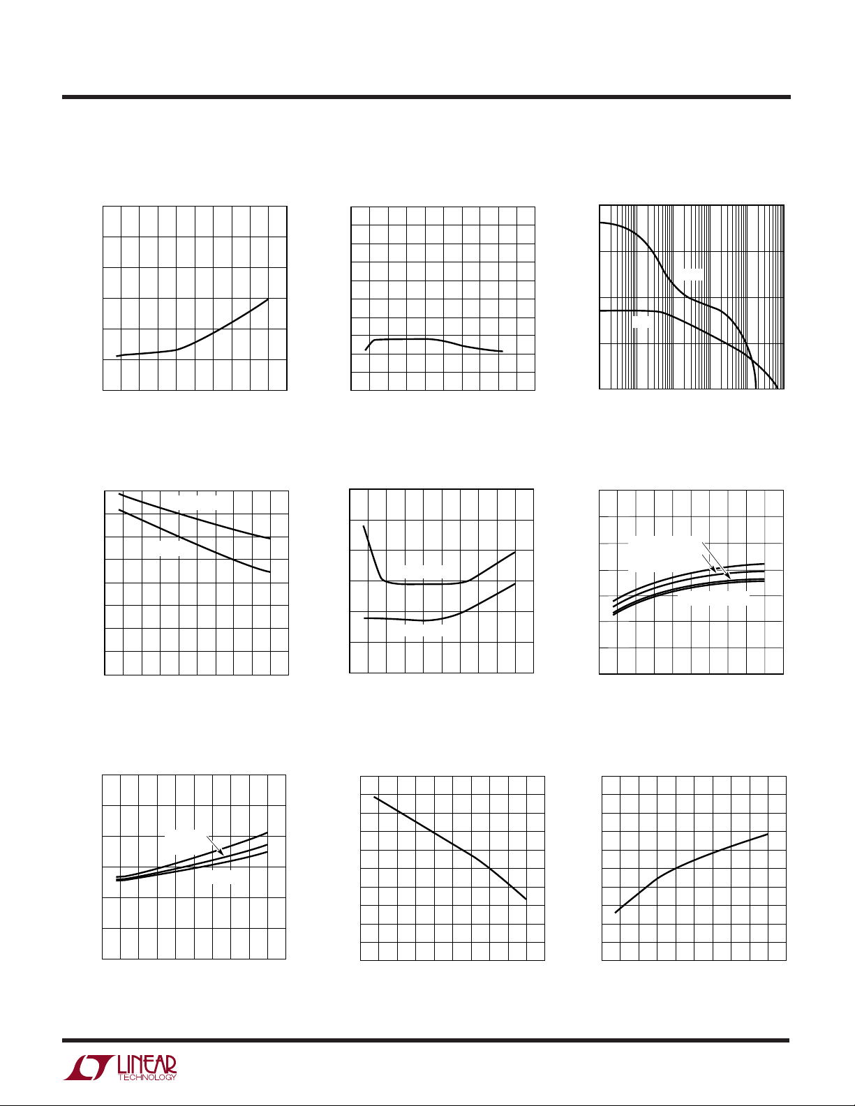
FREQUENCY (Hz)
50
100
ERROR AMPLIFIER GAIN (dB) AND PHASE (DEG)
150
200
1k 100k 1M 100M
3150 G11
0
10k
10M
PHASE
GAIN
TEMPERATURE (°C)
–75
300
I
POS
+ I
NEG
SUPPLY CURRENT (µA)
400
600
700
800
1000
–50
50
100
3150 G14
500
900
25
150
175
–25
0
75 125
I
POS
= I
NEG
= 3V
I
POS
= I
NEG
= 5V
I
POS
= I
NEG
= 12V
I
POS
= I
NEG
= 20V
UW
TYPICAL PERFOR A CE CHARACTERISTICS
LT3150
Linear Regulator Controller
FB2 Line Regulation
vs Temperature
0.030
0.025
0.020
0.015
0.010
FB2 LINE REGULATION (%/V)
0.005
0
–25 25 75 125
TEMPERATURE (°C)
Gate Output Swing Low
vs Temperature
3.00
2.75
2.50
2.25
2.00
1.75
1.50
GATE OUTPUT SWING LOW (V)
1.25
1.00
–50 150
–75
I
LOAD
NO LOAD
–25
0
25
TEMPERATURE (°C)
= 50mA
75
50
100
125
3150 G09
3150 G12
175–50–75 0 50 100 150
175
Error Amplifier Large-Signal
Voltage Gain vs Temperature
120
115
110
105
100
95
90
85
80
LARGE-SIGNAL VOLTAGE GAIN (dB)
75
70
–25
–50 150
–75
0
25
50
TEMPERATURE (°C)
Gate Output Swing High (V
V
) vs Temperature
GATE
3.0
2.5
2.0
I
= 50mA
1.5
1.0
GATE OUTPUT SWING HIGH (V)
0.5
0
LOAD
NO LOAD
–25 25 75 125
TEMPERATURE (°C)
Gain and Phase vs Frequency
75
100
125
175
3150 G10
I
+ I
IN2
–
POS
Supply Current
NEG
vs Temperature
175–50–75 0 50 100 150
3150 G13
Current Limit Threshold Voltage
vs Temperature
65
60
I
55
50
45
40
CURRENT LIMIT THRESHOLD VOLTAGE (mV)
35
–25 25 75 125
= 5V
POS
= 3V
I
POS
TEMPERATURE (°C)
I
POS
= 20V
3150 G15
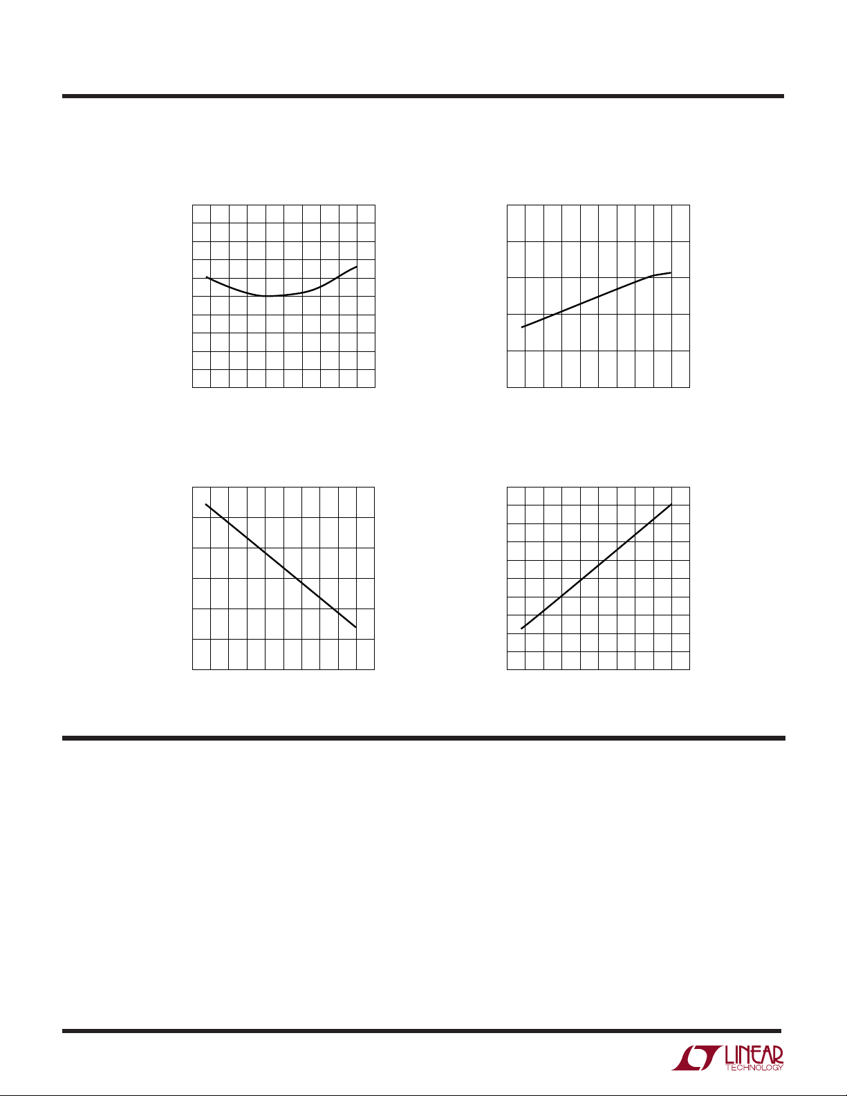
Current Limit Threshold Voltage
Line Regulation vs Temperature
0
–0.1
–0.2
–0.3
–0.4
CURRENT LIMIT THRESHOLD
VOLTAGE LINE REGULATION (%/V)
175–50–75 0 50 100 150
–0.5
–25
0
–50 150
–75
25
50
TEMPERATURE (°C)
75
100
125
175
3150 G16
SHDN2 Sink Current
vs Temperature
7.5
7.0
6.5
6.0
5.5
5.0
4.5
4.0
SHDN2 SINK CURRENT (µA)
3.5
3.0
2.5
–25
–50 150
–75
0
25
TEMPERATURE (°C)
75
100
125
50
175
3150 G17
3150f
5
LT3150
UW
TYPICAL PERFOR A CE CHARACTERISTICS
Linear Regulator Controller
SHDN2 Source Current
vs Temperature
–10
–11
–12
–13
–14
–15
–16
–17
–18
SHDN2 SOURCE CURRENT (µA)
–19
–20
–25
–50 150
–75
0
25
50
TEMPERATURE (°C)
SHDN2 High Clamp Voltage
vs Temperature
2.1
2.0
1.9
1.8
1.7
1.6
SHDN2 HIGH CLAMP VOLTAGE (V)
1.5
–25 25 75 125
TEMPERATURE (°C)
SHDN2 Low Clamp Voltage
vs Temperature
0.25
0.20
0.15
0.10
0.05
SHDN2 LOW CLAMP VOLTAGE (V)
75
100
125
175
3150 G18
0
–25
–50 150
–75
0
TEMPERATURE (°C)
75
25
50
100
125
175
3150 G19
SHDN2 Hysteresis vs Temperature
150
140
130
120
110
100
90
80
SHDN2 HYSTERESIS (mV)
70
60
3150 G20
175–50–75 0 50 100 150
50
–25
–50 150
–75
0
TEMPERATURE (°C)
75
25
100
50
125
175
3150 G21
U
UU
PI FU CTIO S
SW (Pin 1): Boost Converter Switch Pin. Connect inductor/diode here. Minimize trace area at this pin to keep EMI
down.
SWGND (Pin 2): Switch Ground. Tie directly to the local
ground plane and the GNDs at Pins 6 and 15.
V
(Pin 3): Boost Converter Input Supply Pin. Must be
IN1
locally bypassed.
SHDN2 (Pin 4): This is a multifunction shutdown pin that
provides GATE drive latchoff capability. A 15µA current
source, that turns on when current limit is activated,
6
charges a capacitor placed in series with SHDN2 to GND
and performs a current limit time-out function. The pin is
also the input to a comparator referenced to V
When the pin pulls above V
, the comparator latches the
REF
(1.21V).
REF
gate drive to the external MOSFET off. The comparator
typically has 100mV of hysteresis and the SHDN2 pin can
be pulled low to reset the latchoff function. This pin
provides overvoltage protection or thermal shutdown
protection when driven from various resistor divider
schemes.
3150f

LT3150
U
UU
PI FU CTIO S
V
(Pin 5): This is the input supply for the linear regulator
IN2
control circuitry and provides sufficient gate drive compliance for the external N-channel MOSFET. The maximum
operating V
set by V
(worst-case V
GND (Pin 6): Analog Ground. This pin is also the negative
sense terminal for the internal 1.21V reference. Connect the
LDO regulator external feedback divider network and frequency compensation components that terminate to GND
directly to this pin for best regulation and performance. Also,
tie this pin directly to SWGND (Pin 2) and GND (Pin 15).
NC (Pins 7, 10): No Connect.
FB2 (Pin 8): This is the inverting input of the error amplifier
for the linear regulator. The noninverting input is tied to the
internal 1.21V reference. Input bias current for this pin is
typically 0.6µA flowing out of the pin. Tie this pin to a
resistor divider network to set output voltage. Tie the top
of the external resistor divider directly to the output load
for best regulation performance.
COMP (Pin 9): This is the high impedance gain node of the
error amplifier and is used for external frequency compensation. The transconductance of the error amplifier is 15
millimhos and open-loop voltage gain is typically 84dB.
Frequency compensation is generally performed with a
series RC + C network to ground.
GATE (Pin 11): This is the output of the error amplifier
that drives N-channel MOSFETs with up to 5000pF of
“effective” gate capacitance. The typical open-loop output impedance is 2Ω. When using low input capacitance
MOSFETs (< 1500pF), a small gate resistor of 2Ω to 10Ω
dampens high frequency ringing created by an LC resonance due to the MOSFET gate’s lead inductance and
input capacitance. The GATE pin delivers up to 50mA for
a few hundred nanoseconds when slewing the gate of the
N-channel MOSFET in response to output load current
transients.
is 20V and the minimum operating V
IN2
+ (VGS of the MOSFET at max I
OUT
to GATE output swing).
IN2
OUT
is
IN2
) + 1.6V
I
(Pin 12): This is the negative sense terminal of the
NEG
current limit amplifier. A small sense resistor is connected
in series with the drain of the external MOSFET and is
connected between the I
POS
and I
pins. A 50mV
NEG
threshold voltage in conjunction with the sense resistor
value sets the current limit level. The current sense resistor can be a low value shunt or can be made from a piece
of PC board trace. If the current limit amplifier is not used,
tie the I
is to ground the I
NEG
pin to I
to defeat current limit. An alternative
POS
pin. This action disables the current
NEG
limit amplifier and additional internal circuitry activates
the timer circuit on the SHDN2 pin if the GATE pin swings
to the VIN rail. This option provides the user with a
No R
I
POS
TM
SENSE
current limit function.
(Pin 13): This is the positive sense terminal of the
current limit amplifier. Tie this pin directly to the main
input voltage from which the output voltage is regulated.
SHDN1 (Pin 14): Boost Regulator Shutdown Pin. Tie to 1V
or more to enable device. Ground to shut down. This pin
must not float for proper operation. Connect SHDN1
externally as it does not incorporate an internal pull-up or
pull-down.
GND (Pin 15): Boost Converter Analog Ground. This pin
is also the negative sense terminal for the FB1 1.23V
reference. Connect the external feedback divider network, which sets the V
supply voltage and terminates
IN2
to GND, directly to this pin for best regulation and
performance. Also, tie this pin directly to SWGND (Pin 2)
and GND (Pin 6).
FB1 (Pin 16): Boost Regulator Feedback Pin. Reference
voltage is 1.23V. Connect resistive divider tap here.
Minimize trace area at FB1. Set V
V
= 1.23V(1 + R1/R2).
OUT
No R
is a trademark of Linear Technology Corporation.
SENSE
OUT
= V
IN2
according to
3150f
7

LT3150
W
BLOCK DIAGRA S
Boost Switching Regulator
V
IN2
R1
(EXTERNAL)
R2
(EXTERNAL)
V
OUT
V
3
IN1
FB1
16
FB1
GND
15
SHDN2
R7
(EXTERNAL)
FB2
R8
(EXTERNAL)
V
GND
FB2
4
IN2
5
6
8
V
IN1
Q2
x10
R6
40k
R3
30k
R4
140k
+
A1
–
gm = 77µmhos
R
C
100k
C
40pF
C
RAMP
GENERATOR
1.4MHz
OSCILLATOR
Σ
SHDN1
14
COMPARATOR
–
A2
+
SHUTDOWN
FF
RQ
S
I
LIM1
DRIVER
SW
1
Q3
+
0.15Ω
–
2
SWGND
3150 BD1
R5
40k
Q1
Linear Regulator Controller
V
TH1
SW1
I
1
15µA
NORMALLY
OPEN
OR1
50mV
+
–
+
I
AMP
LIM2
D1
–
I
I
POS
13
NEG
12
+
COMP1
–
100mV
HYSTERESIS
D2
–
COMP2
+
SW2
I
2
5µA
NORMALLY
CLOSED
R10
OR2
Q9
5k
+
V
START-UP V
REF
1.21V
100µA
COMP3
+
ERROR AMP
–
I
3
Q5Q4
R9
50k
Q7
Q6
TH2
1V
–
+
–
GATE
11
COMP
9
Q8
3150 BD02
8
3150f

WUUU
APPLICATIO S I FOR ATIO
LT3150
INTRODUCTION
With each new generation of computing systems, total
power increases while system voltages fall. CPU core,
logic and termination supplies below 1.8V are now common. Power supplies must not only regulate low output
voltages, but must also operate from low input voltages.
A low voltage, very low dropout linear regulator is an
attractive conversion option for applications with output
current in the range of several amperes. Component count
and cost are low in comparison with switching regulator
solutions and with low input-to-output differential voltages, efficiencies are comparable.
In addition to low input-to-output voltage conversion,
these systems require stringent output voltage regulation.
The output voltage specification includes input voltage
change, output load current change, temperature change
and output load current transient response. Total tolerances as low as ±2% are now required. For a 1.5V output
voltage, this amounts to a mere ±30mV. Transient load
current response is the most critical component as output
current can cycle from zero to amps in tens of nanoseconds. These requirements mandate the need for a very
accurate, very high speed regulator.
Historically employed solutions include monolithic
3-terminal linear regulators, PNP transistors driven by
low cost control circuits and simple buck converter
switching regulators. The 3-terminal regulator provides
high integration, the PNP driven regulator provides low
dropout performance and the switching regulator provides high electrical efficiency.
However, these solutions manifest a common trait of
transient response measured in many microseconds. This
fact translates to a regulator output decoupling capacitor
scheme requiring several hundred microfarads of very low
ESR bulk capacitance using multiple capacitors in parallel.
This required bulk capacitance is in addition to the ceramic
decoupling capacitor network that handles the transient
load response during the first few hundred nanoseconds
as well as providing high frequency noise immunity. The
combined cost of all capacitors is a significant percentage
of the total power supply cost.
The LT3150 controller IC is a unique, easy-to-use device
that drives an external N-channel MOSFET as a source
follower and realizes an extremely low dropout, ultrafast
transient response regulator. The circuit achieves superior regulator bandwidth and transient load performance
by eliminating expensive special polymer, tantalum or
bulk electrolytic capacitors in the most demanding applications. Performance is optimized around the latest generation of low cost, low ESR, readily available ceramic
capacitors. Users benefit directly by saving significant
cost as all bulk capacitance is removed. Additional savings
include insertion cost, purchasing/inventory cost and
board space.
The precision-trimmed adjustable voltage LT3150 accommodates most power supply voltages. Proper selection of the N-channel MOSFET R
dropout voltage performance. Transient load step performance is optimized for ceramic output capacitor networks
allowing the regulator to respond to transient load changes
in a few hundred nanoseconds. The output capacitor
network typically consists of multiple 1µF to 10µF ceramic
capacitors in parallel depending on the power supply
requirements. The LT3150 also incorporates current limiting, on/off control for power supply sequencing and
overvoltage protection or thermal shutdown with simple
external components.
The LT3150 combines the benefits of low input voltage
operation, very low dropout voltage performance, precision regulation and fast transient response. With low
input/output differential voltage applications becoming
the norm, an LT3150-based solution is a practical alternative to switching regulators providing comparable efficiency performance at an appreciable cost savings.
BLOCK DIAGRAM OPERATION
Gate drive for the external N-channel MOSFET in the linear
regulator loop is provided by a current mode, internally
compensated, fixed frequency step-up switching regulator. Referring to the Block Diagram, Q1 and Q2 form a
bandgap reference core whose loop is closed around the
output of the regulator. The voltage drop across R5 and R6
allows user-settable
DS(ON)
3150f
9

LT3150
WUUU
APPLICATIO S I FOR ATIO
is low enough such that Q1 and Q2 do not saturate, even
when V
above 1.23V, causing VC (the error amplifier’s output) to
decrease. Comparator A2’s output stays high, keeping
switch Q3 in the off state. As increased output loading
causes the FB1 voltage to decrease, A1’s output increases.
Switch current is regulated directly on a cycle-by-cycle
basis by the VC node. The flip flop is set at the beginning
of each switch cycle, turning on the switch. When the
summation of a signal representing switch current and a
ramp generator (introduced to avoid subharmonic oscillations at duty factors greater than 50%) exceeds the V
signal, comparator A2 changes state, resetting the flip flop
and turning off the switch. More power is delivered to the
output as switch current is increased. The output voltage,
attenuated by external resistor divider R1 and R2, appears
at the FB1 pin, closing the overall loop. Frequency compensation is provided internally by RC and CC. Transient
response can be optimized by the addition of a phase lead
capacitor CPL in parallel with R1 in applications where
large value or low ESR output capacitors are used.
As the load current is decreased, the switch turns on for a
shorter period each cycle. If the load current is further
decreased, the converter will skip cycles to maintain
output voltage regulation.
The linear regulator controller section of the LT3150 Block
Diagram consists of a simple feedback control loop and
multiple protection functions. Examining the Block Diagram for the LT3150, a start-up circuit provides controlled
start-up, including the precision-trimmed bandgap reference, and establishes all internal current and voltage
biasing.
Reference voltage accuracy at the FB2 pin is specified as
±0.6% at room temperature and as ±1% over the full
operating temperature range. This places the LT3150
among a select group of regulators with a very tightly
specified reference voltage tolerance. The 1.21V reference
is tied to the noninverting input of the main error amplifier
in the feedback control loop.
The error amplifier consists of a single high gain gm stage
with a transconductance equal to 15 millimhos. The
inverting terminal is brought out as the FB2 pin. The g
stage provides differential-to-single ended conversion at
is 1V. When there is no load, FB1 rises slightly
IN1
C
m
the COMP pin. The output impedance of the gm stage is
about 1MΩ and thus, 84dB of typical DC error amplifier
open-loop gain is realized along with a typical 75MHz
uncompensated unity-gain crossover frequency. Note
that the overall feedback loop’s DC gain decreases from
the gain provided by the error amplifier by the attenuation
factor in the resistor divider network which sets the DC
output voltage. External access to the high impedance
gain node of the error amplifier permits typical loop
compensation to be accomplished with a series RC + C
network to ground.
A high speed, high current output stage buffers the COMP
node and drives up to 5000pF of “effective” MOSFET gate
capacitance with almost no change in load transient performance. The output stage delivers up to 50mA peak
when slewing the MOSFET gate in response to load
current transients. The typical output impedance of the
GATE pin is typically 2Ω. This pushes the pole due to the
error amplifier output impedance and the MOSFET input
capacitance well beyond the loop crossover frequency.
the capacitance of the MOSFET used is less than 1500pF,
it may be necessary to add a small value series gate
resistor of 2Ω to 10Ω. This gate resistor helps damp the
LC resonance created by the MOSFET gate’s lead inductance and input capacitance. In addition, the pole formed
by this resistance and the MOSFET input capacitance can
be fine tuned.
Because the MOSFET pass transistor is connected as a
source follower, the power path gain is much more predictable than designs that employ a discrete PNP transistor as
the pass device. This is due to the significant production
variations encountered with PNP Beta. MOSFETs are also
very high speed devices which enhance the ability to produce a stable wide bandwidth control loop. An additional
advantage of the follower topology is inherently good line
rejection. Input supply disturbances do not propagate
through to the output. The feedback loop for a regulator
circuit is completed by providing an error signal to the FB2
pin. A resistor divider network senses the output voltage
and sets the regulated DC bias point. In general, the LT3150
regulator feedback loop permits a loop crossover frequency
on the order of 1MHz while maintaining good phase and gain
margins. This unity-gain frequency is a factor of 20 to 30
times the bandwidth of currently implemented regulator
If
3150f
10

WUUU
APPLICATIO S I FOR ATIO
LT3150
solutions for microprocessor power supplies. This significant performance benefit is what permits the elimination
of all bulk output capacitance.
Several other unique features are included in the design
that increase its functionality and robustness. These functions comprise the remainder of the Block Diagram.
A high side sense, current limit amplifier provides active
current limiting for the regulator. The current limit amplifier uses an external low value shunt resistor connected in
series with the external MOSFET’s drain. This resistor can
be a discrete shunt resistor or can be manufactured from
a Kelvin-sensed section of “free” PC board trace. All load
current flows through the MOSFET drain and thus, through
the sense resistor. The advantage of using high side
current sensing in this topology is that the MOSFET’s gain
and the main feedback loop’s gain remain unaffected. The
sense resistor develops a voltage equal to I
The current limit amplifier’s 50mV threshold voltage is a
good compromise between power dissipation in the sense
resistor, dropout voltage impact and noise immunity.
Current limit activates when the sense resistor voltage
equals the 50mV threshold.
Two events occur when current limit activates: the first is
that the current limit amplifier drives Q5 in the Block
Diagram and clamps the positive swing of the COMP node
in the main error amplifier to a voltage that provides an
output load current of 50mV/R
ues as long as the output current overload persists. The
second event is that a timer circuit activates at the SHDN2
pin. This pin is normally held low by a 5µA active pull-down
that limits to ≈ 100mV above ground. When current limit
activates, the 5µA pull-down turns off and a 15µA pull-up
current source turns on. Placing a capacitor in series with
the SHDN2 pin to ground generates a programmable time
ramp voltage.
The SHDN2 pin is also the positive input of COMP1. The
negative input is tied to the internal 1.21V reference.
When the SHDN2 pin ramps above V
drives Q7 and Q8. This action pulls the COMP and GATE
pins low and latches the external MOSFET drive off. This
condition reduces the MOSFET power dissipation to zero.
The time period until the latched-off condition occurs is
typically equal to C
(1.11V)/15µA. For example, a
SHDN2
. This action contin-
SENSE
REF
OUT(RSENSE
, the comparator
).
1µF capacitor on the SHDN2 pin yields a 74ms ramp time.
In short, this unique circuit block performs a current limit
time-out function that latches off the regulator drive after
a predefined time period. The time-out period selected is
a function of system requirements including start-up and
safe operating area. The SHDN2 pin is internally clamped
to typically 1.85V by Q9 and R10. The comparator tied to
the SHDN2 pin has 100mV of typical hysteresis to provide
noise immunity. The hysteresis is especially useful when
using the SHDN2 pin for thermal shutdown.
Restoring normal operation after the load current fault is
cleared is accomplished in two ways. One option is to
recycle the V
external bleed path for the SHDN2 pin capacitor is provided. The second option is to provide an active reset
circuit that pulls the SHDN2 pin below V
SHDN2 pin below V
source and reactivates the 5µA pull-down. If the SHDN2
pin is held below V
lator continues to operate in current limit into a short. This
action requires being able to sink 15µA from the SHDN2
pin at less than 1V. The 5µA pull-down current source and
the 15µA pull-up current source are designed low enough
in value so that an external resistor divider network can
drive the SHDN2 pin to provide overvoltage protection or
to provide thermal shutdown with the use of a thermistor
in the divider network. Diode-ORing these functions together is simple to accomplish and provides multiple
functionality for one pin.
If the current limit amplifier is not used, two choices
present themselves. The simplest choice is to tie the I
pin directly to the I
and provides the simplest, no frills circuit. Applications in
which the current limit amplifier is not used are where
extremely low dropout voltages must be achieved and the
50mV threshold voltage cannot be tolerated.
However, a second available choice permits a user to provide short-circuit protection with no external sensing. This
technique is activated by grounding the I
disables the current limit amplifier because Schottky diode
D1 clamps the amplifier’s output and prevents Q5 from
pulling down the COMP node. In addition, Schottky diode
D2 turns off pull-down transistor Q4. Q4 is normally on and
LT3150 supply voltage as long as an
IN2
. Pulling the
REF
turns off the 15µA pull-up current
REF
during a fault condition, the regu-
REF
pin. This action defeats current limit
POS
pin. This action
NEG
NEG
3150f
11

LT3150
WUUU
APPLICATIO S I FOR ATIO
holds internal comparator COMP3’s output low. This
comparator circuit, now enabled, monitors the GATE pin
and detects saturation at the positive rail. When a saturated
condition is detected, COMP3 activates the shutdown timer.
Once the time-out period occurs, the output is shut down
and latched off. The operation of resetting the latch remains
the same. Note that this technique does not limit the FET
current during the time-out period. The output current is
only limited by the input power supply and the input/output impedance. Setting the timer to a short period in this
mode of operation keeps the external MOSFET within its
SOA (safe operating area) boundary and keeps the
MOSFET’s temperature rise under control.
Unique circuit design incorporated into the LT3150 alleviates all concerns about power supply sequencing. The
issue of power supply sequencing is an important topic as
the typical LT3150 application has two separate power
supply inputs, V
IN1
and V
. If the V
IN2
supply
IN2
voltage is
slow in ramping up or is held off by SHDN1, insufficient
MOSFET gate drive exists and therefore, the output
voltage does not come up. This statement is true as long
as the V
input voltage is lower than the threshold of the
IN1
external MOSFET. Prior to the boost converter powering
up, V
through the boost inductor. If V
equals V
IN2
– VF due to the DC path present
IN1
is high enough, the
IN1
MOSFET turns on and pulls the output voltage up. If this
situation exists and the output must be held off, then
pulling the SHDN2 pin high actively holds the output off.
Pull the SHDN2 pin low to allow start-up, as the SHDN2
high logic state is a latched condition.
If V
is present, but the V
IN2
I
pin is slow in ramping, then the feedback loop wants
POS
to drive the GATE pin to the positive V
in a large current as the V
supply voltage tied to the
IN1
rail. This results
IN2
supply ramps up. However,
IN1
undervoltage lockout circuit COMP2, which monitors the
I
supply voltage, holds Q6 on and pulls the COMP pin
POS
low until the I
voltage increases to greater than the
POS
internal 1.21 reference voltage. The undervoltage lockout
circuit then smoothly releases the COMP pin and allows
the output voltage to come up in dropout from the input
supply voltage. An additional benefit derived from the
speed of the LT3150 feedback loop is that turn-on
overshoot is virtually nonexistent in a properly compensated system.
BOOST REGULATOR COMPONENT SELECTION
Diode
Linear Technology recommends the use of a Schottky
diode with the LT3150. For input supply voltages less than
2V, the Motorola MBR0520 or equivalent is a good choice
due to its small size, low cost and low forward voltage. The
average diode current equals the V
supply current of
IN2
12mA typically. The peak diode current equals the peak
switch current, which in these low input-to-output voltage
applications ranges from 100mA to 200mA.
The diode’s forward voltage during its conduction period
directly affects the duty cycle of the boost converter. These
low input-to-output voltage applications require the boost
converter to operate at duty cycles close to the maximum
and the difference of a few hundred millivolts in the diode
forward voltage results in a duty cycle difference of several
percent. For supply voltages greater than 2V, a 1N4148 is
suitable and lowers cost.
Inductor
Use inductors with a saturation current rating (where
inductance is approximately 70% of zero current inductance) of 0.2A or greater. Also, choose an inductor with a
DCR of 2.5Ω or less. The inductor’s DCR also affects the
boost converter’s duty cycle. A larger DCR value increases
the required duty cycle. An inductance value between
4.7µH and 10µH works well in most applications.
Table 1 lists several 10µH inductors that work with the
LT3150, although this is by no means an exhaustive list.
Many magnetic vendors have components suitable for use
in this boost application.
Input Capacitor
The input bypass capacitors serve as the reservoir capacitor for the boost regulator, the linear regulator and whatever other system circuitry the input supply powers.
Therefore, the input capacitor network is most likely
distributed along the input supply PCB plane.
However, the switching of current at high speed by the
boost regulator mandates a local bypass capacitor at the
V
pin. Place this input capacitor physically close to the
IN1
3150f
12

LT3150
WUUU
APPLICATIO S I FOR ATIO
Table 1. Inductor Vendors
VENDOR PHONE URL PART NUMBER INDUCTANCE DCR I
Murata (404) 436-1300 www.murata.com LQH31CN100K03K 10µH 1.3Ω 0.23A
LQH32CN100K23K 10µH 0.44Ω 0.3A
Panasonic (800) 344-2112 www.panasonic.com ELJPC100KF 10µH 2.2Ω 0.21A
Sumida (847) 956-0666 www.sumida.com CDRH3D16100 10µH 0.21Ω 0.55A
Taiyo Yuden (800) 348-2496 www.t-yuden.com LQLB2016T100M 10µH 0.5Ω 0.155A
LQLB2518T100M 10µH 0.25Ω 0.165A
Toko (847) 297-0070 www.toko.com LLM3225-100K 10µH 1.7Ω 0.22A
V
pin. ESR is not critical and in most cases, an inexpen-
IN1
sive tantalum or ceramic capacitor with a value from 1µF
to 4.7µF is appropriate.
The boost regulator output capacitor also serves as the
V
input bypass capacitor. Place this capacitor physi-
IN2
cally close to the V
pin. This capacitor supplies the
IN2
instantaneous current to slew the external MOSFET’s
Output Capacitor
The output capacitor choice is far more important. The
gate capacitance quickly during an output load current
transient.
capacitor’s characteristics determines output voltage ripple.
The output capacitor must have enough capacitance to
LINEAR REGULATOR COMPONENT SELECTION
satisfy the load under transient conditions and it must
shunt the switched component of current coming through
the diode. Output voltage ripple results because this
switched current passes through the capacitor’s finite
output impedance. The capacitor must have low impedance at the 1.4MHz switching frequency of the LT3150. At
this frequency, the capacitor’s equivalent series resistance (ESR) usually dominates the impedance. Choosing
a capacitor with lower ESR results in lower output voltage
ripple.
However, consider loop stability when choosing the output capacitor because the LT3150 is internally compensated and no access is provided to this internal
compensation. Small, low cost tantalum capacitors have
some ESR. This ESR enhances stability due to the addition
of a zero in the regulator feedback loop. Ceramic capacitors are very popular, having attractive characteristics
such as near-zero ESR, small size and low cost. Replacing
the tantalum output capacitor with a ceramic unit decreases the phase margin, in some cases to unacceptable
levels. The addition of a phase lead capacitor and an
isolating resistor in the feedback divider network can be
used to stabilize the feedback loop, but the added component count and cost makes the use of a tantalum output
capacitor the simpler and preferred choice.
Output Capacitors
The LT3150 linear regulator is stable with a wide range of
output capacitors (assuming the feedback loop is properly frequency compensated). However, using multiple,
low value, very low ESR ceramic capacitors (1µF to 4.7µF)
in parallel optimizes the load transient response of an
LT3150 feedback loop. As is discussed in the Frequency
Compensation section, the output capacitor value is critical because it sets the location of a pole in the feedback
loop that determines the unity-gain crossover frequency.
Therefore, the characteristics of ceramic capacitors warrant some discussion.
Manufacturers make ceramic capacitors with a variety of
dielectrics, each with different behavior across temperature and applied voltage. The most common dielectrics
are Z5U, Y5V, X5R and X7R. The Z5U and Y5V dielectrics
provide high C-V products in a small package at low cost,
but exhibit very strong voltage and temperature coefficients. The X5R and X7R dielectrics yield highly stable
characteristics and are more suitable for use as the output
capacitor at fractionally increased cost. The X5R and X7R
dielectrics both exhibit excellent voltage coefficient char
teristics. The X7R type works over a larger temperature
range and exhibits better temperature stability whereas
X5R is less expensive and is available in higher values.
SAT
ac-
3150f
13

LT3150
WUUU
APPLICATIO S I FOR ATIO
Figures 1 and 2 show voltage coefficient and temperature
coefficient comparisons between Y5V and X5R material.
With the critical pole in the LT3150 feedback loop being set
by the absolute value of the output capacitor, it is obvious
why Linear Technology strongly recommends the use of
ceramic capacitors with X5R or X7R dielectric material.
MOSFET Selection
MOSFET selection criteria include threshold voltage
V
tance R
package thermal resistance R
, maximum continuous drain current ID, on-resis-
GS(TH)
, maximum drain-to-source voltage VDS and
DS(ON)
.
TH(JA)
Linear Technology recommends the use of a logic-level
threshold MOSFET in LT3150 applications. The VGS range,
as defined by the threshold voltage and the load current
range, fits well within the boost regulator’s capability and
the output swing range of the error amplifier. The MOSFET’s
continuous drain current rating must equal or exceed the
maximum load current and the maximum drain-to-source
voltage must exceed the maximum input voltage.
The most critical specification is the MOSFET R
Calculate the required R
MOSFET R
DS(ON)
≤
from the following formula:
DS(ON)
VV
IN MIN OUT MIN
–
() ()
I
•3
OUT MAX
()
DS(ON)
.
The additional factor of three in the equation’s denominator accounts for production variation, the temperature
coefficient of R
, voltage dips in VIN during transient
DS(ON)
output load steps and other operating point characteris-
tics. Although the factor of three is slightly conservative,
this imposes no cost penalty. As an example, consider the
1.8V to 1.5V at 4A application on the front page. Assuming
the 1.8V input and the 1.5V output each have a ±5%
tolerance,
(. • . )–(. • . )
R
DS(ON)
095 18 095 15
=≤Ω
A Siliconix Si4410 MOSFET with an R
close match. Although the Si4410’s 30V maximum V
VV
•
34
A
DS(ON)
.
23 8
m
of 20mΩ is a
DS
and 8A maximum ID ratings exceed the application’s
requirements, the Si4410’s low cost makes it an excellent
choice.
As the final criteria, consider the thermal resistance R
TH(JA)
of the MOSFET’s package. The temperature rise in the
MOSFET must be kept under control and within the
manufacturer’s maximum junction temperature specification. The power dissipated in the MOSFET is calculated by:
P
In the design example, P
1.2W. The Si4410’s R
MOSFET
= (V
IN
– V
) • I
OUT
TH(JA)
OUT
MOSFET
= (1.8V – 1.5V) • 4A =
is 50°C/W for its S0-8 pack-
age, which translates to a 60°C temperature rise above
ambient. MOSFET manufacturers have significantly lowered the thermal resistance of modern devices with improved packages. These packages provide exposed
backsides that directly transfer heat to the PCB board.
These packages enable LT3150 applications with much
higher output currents while keeping the MOSFET temperature in control.
20
0
–20
–40
–60
CHANGE IN VALUE (%)
–80
–100
0
Figure 1. Ceramic Capacitor DC Bias Characteristics
BOTH CAPACITORS ARE 16V,
1210 CASE SIZE, 10µF
X5R
Y5V
26
4
8
DC BIAS VOLTAGE (V)
14
12
10
3150 F01
14
40
20
0
–20
–40
–60
CHANGE IN VALUE (%)
–80
–100
–50
16
Figure 2. Ceramic Capacitor Temperature Characteristics
–25 0
BOTH CAPACITORS ARE 16V,
1210 CASE SIZE, 10µF
X5R
Y5V
50 100 125
25 75
TEMPERATURE (°C)
3150 F02
3150f

WUUU
APPLICATIO S I FOR ATIO
LT3150
Frequency Compensation
Frequency compensation is the most critical step in designing an LT3150 application circuit. Frequency compensation stabilizes the feedback loop under all line, load and
temperature conditions and determines the transient load
step performance.
To start the frequency compensation process, gather the
following application information. Determine the output
voltage, the minimum and maximum output currents, the
transconductance (gfs) of the selected MOSFET at the
minimum and maximum output currents and the output
capacitor type (ceramic, tantalum, electrolytic).
Frequency compensation is accomplished with a passive
network tied from the LT3150’s COMP pin to ground. The
LT3150 generally employs a Type-2 frequency compensation method. The “Type-2” method uses two poles and one
zero. The output capacitor type determines how the zero
in the feedback loop is set. Ceramic capacitors typically
have very low ESR (equivalent series resistance) and
therefore the COMP pin network sets the “zero” location.
Tantalum and electrolytic capacitors typically have sufficient ESR such that the “zero” formed by the ESR and the
capacitance value is used. Using tantalum or electrolytic
capacitors in LT3150 applications is somewhat more
challenging because the user must choose capacitors with
the proper ESR plus capacitance value to place the zero at
the correct spot in the frequency response.
Refer to the simplified LT3150 block diagram shown in
Figure 3 during the frequency compensation discussion
that follows.
Figure 4 illustrates the typical bode plot and the pole/zero
locations with the use of low ESR ceramic output
capacitors.
Figure 5 illustrates the typical bode plot and the pole/zero
locations with the use of tantalum or electrolytic output
capacitors.
In both output capacitor cases, the location of the first
pole, P1, is set by the error amplifier COMP pin’s openloop output impedance, RO, and compensation capacitor,
C1. The low frequency gain is set by g
• RO • (V
m1
REF/VOUT
)
In the case of low ESR ceramic capacitors, R1 in series
with C1 in the COMP pin network sets the zero, Z1. With
tantalum or electrolytic capacitors, the ESR in series with
the output capacitor CO sets Z1. Z1’s location establishes
the mid-band gain or “shelf” gain. For a given value of
output capacitance, the “shelf” gain determines the
regulator’s transient response to an output load step,
especially the output voltage’s peak overshoot and undershoot. For a given output load current change, a corresponding delta in the MOSFET’s VGS occurs. This ∆V
GS
divided by the “shelf gain” sets how much the FB2 must
change and thus, results in output voltage perturbation.
Higher “shelf” gain results in lower transient response
peak deviations. Higher shelf gain also translates to a
g
= 0.015
m1
V
REF
FB2
+
–
Figure 3. Simplified Block Diagram for Frequency Compensation
R
1M
COMP
+
O
R1
C1
C2
–
R
F1
V
R
REF
F2
=
V
RF1 + R
OUT
F2
R
F2
V
R
IN
G
Q1
V
OUT
R
ESR
I
LOAD
C
O
3150 F03
3150f
15

LT3150
WUUU
APPLICATIO S I FOR ATIO
P1 = 1/(2 • π • R
AVOL = g
GAIN (dB)
I
fX = gm1 • R1 • •
• C1)
O
• RO • (V
m1
Z1 = 1/(2 • π • R1 • C1)
LOAD(MIN)
FREQUENCY (Hz)
MANY HIGH ORDER POLES AND
REF/VOUT
P2 = g
m
AV1 = gm1 • R1 • (V
ZEROS PAST UNITY-GAIN f
V
gm(Q1)
REF
2 • π • C
V
OUT
)
P2 IS A FUNCTION
OF LOAD CURRENT
(Q1)/(2 • π • CO)
I
LOAD(MAX)
3150 F04
X
O
REF/VOUT
)
Figure 4. Typical Bode Plot for
Low ESR Ceramic Output Capacitors
higher unity gain bandwidth crossover frequency, fX. f
X
must be set to a value that provides adequate phase and
gain margin and this criteria limits the shelf gain value. If
higher shelf gain is required for a given application, then
increase output capacitance.
In both output capacitor cases, the location of the second
pole, P2, is set by the MOSFET’s transconductance, gm(Q1),
and the value of the output capacitor, CO. The output load
current sets the transconductance of the MOSFET. P2
moves as a function of load current and consequently, so
does the unity-gain crossover frequency, fX. Figures 4 and
5 depict this behavior. At very low output currents, P2’s
location moves to a very low frequency. Therefore, set Z1
at a low enough frequency to provide adequate phase boost.
A temptation is to set Z1’s value equal to P2’s value at
minimum output load current. The bode plot then exhibits
a single pole response at minimum output current. However, this either makes the “shelf gain” and fX too high for
stability or it makes the small signal settling time very long.
Set Z1 above the minimum value for P2 so that at small
output load currents, the second pole P2 occurs and then
Z1 provides phase boost prior to crossing unity gain.
At the highest load current levels, several poles and zeros
exist just beyond the unity-gain crossover frequency.
Sometimes, the gain peaks back above unity and a high
frequency, low level oscillation appears. A high frequency
P1 = 1/(2 • π • R
AVOL = g
GAIN (dB)
I
• C1)
O
• RO • (V
m1
Z1 = 1/(2 • π • ESR • C
LOAD(MIN)
FREQUENCY (Hz)
MANY HIGH ORDER POLES AND
f
X
REF/VOUT
P2 = g
m
AV1 = AVOL • (P1/P2)
ZEROS PAST UNITY-GAIN f
g
m1
=
2 • π • C1
)
P2 IS A FUNCTION
OF LOAD CURRENT
)
O
(Q1)/(2 • π • CO)
• CO)/(gm(Q1) • C1)
= (g
m1
I
LOAD(MAX)
3150 F05
X
Figure 5. Typical Bode Plot for Tantalum
or Electrolytic Output Capacitors
pole is necessary to roll off the response. In the case of
ceramic output capacitors, capacitor C2 in Figure 4 sets
this pole in combination with R1. In the case of electrolytic
or tantalum output capacitors, some small ceramic capacitors in parallel with the main output capacitors usually
provide the desired response.
Finally, look for very high frequency gate oscillations in the
range of 2MHz to 10MHz. Small MOSFETs with low gate
capacitance are most susceptible to this issue. This oscillation is typically caused by the MOSFET’s “effective” gate
capacitance and the MOSFET’s parasitic source inductance resonating. The MOSFET’s source inductance is the
sum of the device’s bond wire plus package lead inductance and the PCB trace inductance between the MOSFET’s
source and the actual output capacitors. Although the
MOSFET’s internal inductance is fixed, proper PCB layout
techniques minimize the external inductance. Minimize
the distance between the MOSFET’s source and the output
decoupling capacitors and run wide planes if possible.
Connect the top of the feedback divider at the point closest
to the actual load rather than the MOSFET source. If high
frequency oscillations persist, a small value resistor in the
range of 1Ω to 50Ω in series with the gate of the MOSFET
typically eliminates this ringing. The inclusion of a gate
resistor may permit the high frequency pole discussed in
the preceding paragraph to be eliminated or fine tuned.
16
3150f

U
TYPICAL APPLICATIO S
LT3150
Setting the Linear Regulator Output Voltage
V
OUT
R2
FB2
R1
= 1.21V(1 + R2/R1)
V
OUT
3150 TA03
Setting Current Limit
I
POS
I
NEG
GATE
= 50mV/R
*I
LIM
R
SENSE
R
SENSE
ACTIVATING CURRENT LIMIT ALSO ACTIVATES
THE SHDN2 PIN TIMER
SENSE
= DISCRETE SHUNT RESISTOR OR
= KELVIN-SENSED PC BOARD TRACE
V
IN1
R
*
SENSE
Q2
V
OUT
3150 TA05
Using No R
I
SHDN2 V
POS
C
T
I
NEG
GATE
Current Limit
SENSE
MBR0520L
C1
10µF
D1
IN1
Q1
V
OUT
3150 TA04
Current Limit with Foldback Limiting Example
I
POS
I
NEG
GATE
SET R5 << R6
50mV
= –
I
OUT
R4
R5
D1
1N4148
D2
1N4148
R6
R6
(V
()
R5 + R6
IN1
3150 TA06
– V
R4
R4
Q3
OUT
V
IN1
I
OUT
V
OUT
– 2VF)
R5
()
R5 + R6
Shutdown Time-Out with Reset
R1
100k
Q1
VN2222L
RESET
0V TO 5V
*C1 = 15µA(t)/1.11V
t = SHUTDOWN LATCHOFF TIME
Shutdown Time-Out with Reset
R2
100k
RESET
0V TO 5V
*C2 = 15µA(t)/1.11V
t = SHUTDOWN LATCH-OFF TIME
Q2
2N3904
R3
100k
SHDN2
C1*
3150 TA07
SHDN2
C2*
3150 TA09
Basic Thermal Shutdown
V
IN1
RT1
10k
NTC
SHDN2
R4*
RT1 = DALE NTHS-1206N02
THERMALLY MOUNT RT1
IN CLOSE PROXIMITY
TO THE EXTERNAL
N-CHANNEL MOSFET
*CHOOSE R4 BASED ON
V
IN1
SHUTDOWN TEMPERATURE
Overvoltage Protection
V
V
= 1.21(R6/R5) + 5µA(R6)
OUT(uth)
= 1.11(R6/R5) – 15µA(R6)
V
OUT(lth)
AND REQUIRED THERMAL
3150 TA08
OUT
R6
SHDN2
R5
3150 TA10
3150f
17

LT3150
TYPICAL APPLICATIO S
1.5V to 1.2V, 4A Very Low Dropout Linear Regulator
U
MBR0520L
1.5k
10µH
5.1Ω
L1
V
IN
1.5V
V
OUT
1.2V
4A
50pF
Si4410
+
3150 TA11
C
IN
220µF
2.5V
×2
2.2µF ×10
X5R CERAMIC
0805 CASE
+
C1
4.7µF
5.9k
1%
1.37k
1%
CIN: PANASONIC SP SERIES EEFUE0E221R 20%
C1: AVX TAJA475M020R 20V 20%
L1: MURATA LQH32CN100K11 OR SUMIDA CDRH3D16100
LT3150
V
IN2
FB1
SHDN2
SWGND
GND
GND
SW
V
SHDN1
I
POS
I
NEG
GATE
FB2
COMP
6800pF
IN1
2.5V to 1.8V, 1.7A Low Dropout Linear Regulator
MBR0520L
1.5k
10µH
5.1Ω
L1
V
IN
2.5V
V
OUT
1.8V
1.7A
3150f
50pF
Si4410
499Ω
1%
1020Ω
1%
+
3150 TA11a
C
IN
220µF
4V
×2
2.2µF ×6
X5R CERAMIC
0805 CASE
+
C1
4.7µF
6.65k
1%
1.37k
1%
LT3150
V
IN2
FB1
SHDN2
SWGND
GND
GND
CIN: PANASONIC SP SERIES EEFUE0G221R 20%
C1: AVX TAJA475M020R 20V 20%
L1: MURATA LQH32CN100K11 OR SUMIDA CDRH3D16100
SW
V
IN1
SHDN1
I
POS
I
NEG
GATE
FB2
COMP
6800pF
18

PACKAGE DESCRIPTIO
LT3150
U
GN Package
16-Lead Plastic SSOP (Narrow .150 Inch)
(Reference LTC DWG # 05-08-1641)
.045 ±.005
.254 MIN
RECOMMENDED SOLDER PAD LAYOUT
.007 – .0098
(0.178 – 0.249)
.016 – .050
NOTE:
1. CONTROLLING DIMENSION: INCHES
2. DIMENSIONS ARE IN
3. DRAWING NOT TO SCALE
*DIMENSION DOES NOT INCLUDE MOLD FLASH. MOLD FLASH
SHALL NOT EXCEED 0.006" (0.152mm) PER SIDE
**DIMENSION DOES NOT INCLUDE INTERLEAD FLASH. INTERLEAD
FLASH SHALL NOT EXCEED 0.010" (0.254mm) PER SIDE
(0.406 – 1.270)
INCHES
(MILLIMETERS)
.150 – .165
.0250 TYP.0165 ±.0015
.015
(0.38 ± 0.10)
0° – 8° TYP
± .004
.189 – .196*
(4.801 – 4.978)
16
15
14
12 11 10
13
.229 – .244
(5.817 – 6.198)
12
×
°
45
.053 – .068
(1.351 – 1.727)
.008 – .012
(0.203 – 0.305)
4
3
5
9
678
(0.102 – 0.249)
.0250
(0.635)
BSC
.009
(0.229)
REF
.150 – .157**
(3.810 – 3.988)
.004 – .0098
GN16 (SSOP) 0502
Information furnished by Linear Technology Corporation is believed to be accurate and reliable.
However, no responsibility is assumed for its use. Linear Technology Corporation makes no representation that the interconnection of its circuits as described herein will not infringe on existing patent rights.
3150f
19

LT3150
TYPICAL APPLICATIO
U
1.8V to 1.5V, 4A Very Low Dropout Linear Regulator with No R
MBR0520L
+
CIN: PANASONIC SP SERIES EEFUE0E221R 20%
C1: AVX TAJA475M020R 20V 20%
L1: MURATA LQH32CN100K11 OR SUMIDA CDRH3D16100
C1
4.7µF
6.19k
1%
1.37k
1%
SHDN2
0.01µF
LT3150
V
IN2
FB1
SHDN2
SWGND
GND
GND
SW
V
IN1
SHDN1
I
POS
I
NEG
GATE
FB2
COMP
6800pF
SHDN1
10µF
1.5k
50pF
Current Limiting and Shutdown
SENSE
L1
10µH
10k
BAT54
5.1Ω
RELATED PARTS
PART NUMBER DESCRIPTION COMMENTS
LT1573 UltraFast Transient Response Low Dropout VIN: 2.8V to 10V, V
Regulator PNP Driver, Up to 5A I
LT1575/LT1577 UltraFast Transient Response Low Dropout VIN: 1.5V to 22V, V
Regulator MOSFET Driver, Up to 10A LT1577 is Dual Version, N8, S8 Packages
LT1761 100mA, Low Noise Micropower, LDO VIN: 1.8V to 20V, V
LT1762 150mA, Low Noise Micropower, LDO VIN: 1.8V to 20V, V
LT1763 500mA, Low Noise Micropower, LDO VIN: 1.8V to 20V, V
LT1764/LT1764A 3A, Low Noise, Fast Transient Response, LDO VIN: 2.7V to 20V, V
LT1962 300mA, Low Noise Micropower, LDO VIN: 1.8V to 20V, V
LT1963/LT1963A 1.5A, Low Noise, Fast Transient Response, LDO VIN: 2.1V to 20V, V
LTC3411 1.25A(I
), 4MHz, Synchronous Step-Down 95% Efficiency, VIN: 2.5V to 5.5V, I
OUT
DC/DC Converter I
LTC3412 2.5A(I
), 4MHz, Synchronous Step-Down 95% Efficiency, VIN: 2.5V to 5.5V, I
OUT
DC/DC Converter I
: 200µA, Requires External PNP Transistor, S8 Package
SD
I
: <1µA, Low Noise <20µV
SD
Capacitors, ThinSOT Package
: <1µA, Low Noise <20µV
I
SD
I
: <1µA, Low Noise <20µV
SD
: <1µA,Low Noise <40µV
I
SD
Capacitors, DD, TO220-5 Packages
: <1µA, Low Noise <20µV
I
SD
I
: <1µA, Low Noise <40µV
SD
Capacitors, DD, T0220-5, SOT-223, S8 Packages
: <1µA, MS and DFN Packages
SD
: <1µA, TSSOP16E Package
SD
V
IN
: 1.25A, V
: 2.5A, V
1.8V
V
OUT
1.5V
4A
REF
REF
: 0.8V,
: 0.8V,
C
IN
+
Si4410
243Ω
1%
1020Ω
1%
: 1.265V, Dropout Voltage: 0.35V, IQ: 1.7mA,
OUT
: 1.21V, Dropout Voltage: 0.15V, IQ: 12mA,
OUT
: 1.22V, Dropout Voltage: 0.30V, IQ: 20µA,
OUT
: 1.22V, Dropout Voltage: 0.30V, IQ: 25µA,
OUT
: 1.22V, Dropout Voltage: 0.30V, IQ: 30µA,
OUT
: 1.21V, Dropout Voltage: 0.34V, IQ: 1mA,
OUT
: 1.22V, Dropout Voltage: 0.27V, IQ: 30µA,
OUT
: 1.21V, Dropout Voltage: 0.34V, IQ: 1mA,
OUT
220µF
2.5V
×2
2.2µF ×10
X5R CERAMIC
0805 CASE
3150 TA11a
, Stable with 1µF Ceramic
RMS P-P
, MS8 Package
RMS P-P
, S8 Package
RMS P-P
, “A” Version Stable with Ceramic
RMS P-P
, MS8 Package
RMS P-P
, “A” Version Stable with Ceramic
RMS P-P
OUT
OUT
20
Linear T echnology Corporation
1630 McCarthy Blvd., Milpitas, CA 95035-7417
(408) 432-1900 ● FAX: (408) 434-0507
●
www.linear.com
3150f
LT/TP 1003 1K • PRINTED IN THE USA
LINEAR TECHNOLOGY CORPORATION 2002
 Loading...