

LT3013
250mA, 4V to 80V
Low Dropout Micropower
Linear Regulator with PWRGD
FEATURES
■
Wide Input Voltage Range: 4V to 80V
■
Low Quiescent Current: 65μA
■
Low Dropout Voltage: 400mV
■
Output Current: 250mA
■
No Protection Diodes Needed
■
Adjustable Output from 1.24V to 60V
■
1μA Quiescent Current in Shutdown
■
Stable with 3.3μF Output Capacitor
■
Stable with Aluminum, Tantalum or Ceramic
Capacitors
■
Reverse-Battery Protection
■
No Reverse Current Flow from Output to Input
■
Thermal Limiting
■
Thermally Enhanced 16-Lead TSSOP and
12-Pin (4mm × 3mm) DFN Package
APPLICATIONS
■
Low Current High Voltage Regulators
■
Regulator for Battery-Powered Systems
■
Telecom Applications
■
Automotive Applications
DESCRIPTION
The LT®3013 is a high voltage, micropower low dropout
linear regulator. The device is capable of supplying 250mA
of output current with a dropout voltage of 400mV. Designed
for use in battery-powered or high voltage systems, the low
quiescent current (65μA operating and 1μA in shutdown)
makes the LT3013 an ideal choice. Quiescent current is
also well controlled in dropout.
Other features of the LT3013 include a PWRGD fl ag to
indicate output regulation. The delay between regulated
output level and fl ag indication is programmable with a
single capacitor. The LT3013 also has the ability to operate
with very small output capacitors. The regulator is stable
with only 3.3μF on the output while most older devices
require between 10μF and 100μF for stability. Small ceramic capacitors can be used without any need for series
resistance (ESR) as is common with other regulators.
Internal protection circuitry includes reverse-battery
protection, current limiting, thermal limiting and reverse
current protection.
The device is available with an adjustable output with a
1.24V reference voltage. The LT3013 regulator is available
in the thermally enhanced 16-lead TSSOP and the low
profi le (0.75mm), 12-pin (4mm × 3mm) DFN package,
both providing excellent thermal characteristics.
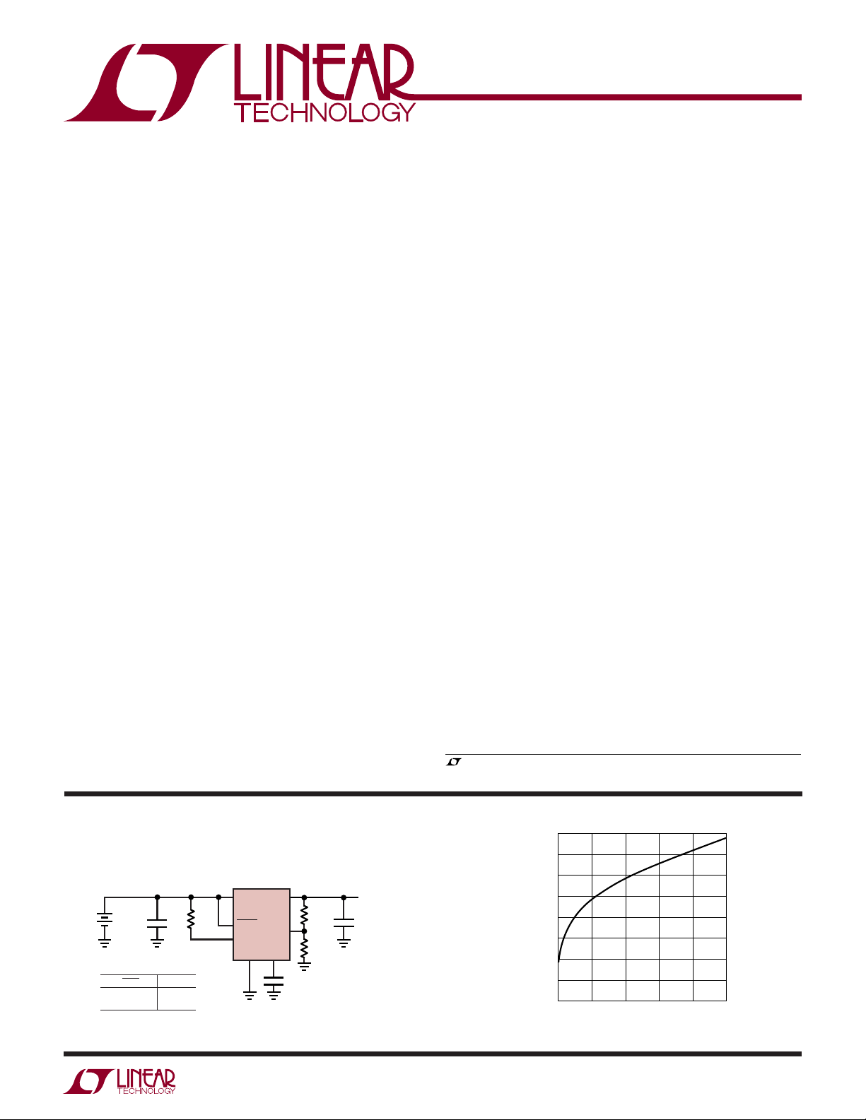
TYPICAL APPLICATION
5V Supply with Shutdown
IN
V
IN
5.4V TO
80V
V
SHDN
<0.3V
>2.0V
1µF
OUTPUT
OFF
ON
1.6M
LT3013
SHDN
PWRGD
GND
C
OUT
ADJ
T
1000pF
750k
249k
3013 TA01
V
5V
250mA
3.3µF
OUT
, LT, LTC and LTM are registered trademarks of Linear Technology Corporation.
All other trademarks are the property of their respective owners.
Dropout Voltage
400
350
300
250
200
150
100
DROPOUT VOLTAGE (mV)
50
0
50 100 150 250
0
OUTPUT CURRENT (mA)
200
3013 TA02
3013fc
1
LT3013
ABSOLUTE MAXIMUM RATINGS
(Note 1)
IN Pin Voltage .........................................................±80V
OUT Pin Voltage ......................................................±60V
IN to OUT Differential Voltage .................................±80V
ADJ Pin Voltage ....................................................... ±7V
⎯S⎯H⎯D⎯
N Pin Input Voltage ..........................................±80V
CT Pin Voltage .................................................7V, –0.5V
PWRGD Pin Voltage .......................................80V, –0.5V
PACKAGE/ORDER INFORMATION
Output Short-Circuit Duration .......................... Indefi nite
Storage Temperature Range
TSSOP Package ................................. –65°C to 150°C
DFN Package ...................................... –65°C to 125°C
Operating Junction Temperature Range
(Notes 3, 10, 11)
LT3013E ............................................. –40°C to 125°C
LT3013HFE ........................................ –40°C to 140°C
Lead Temperature (FE16 Soldering, 10 sec) .........300°C
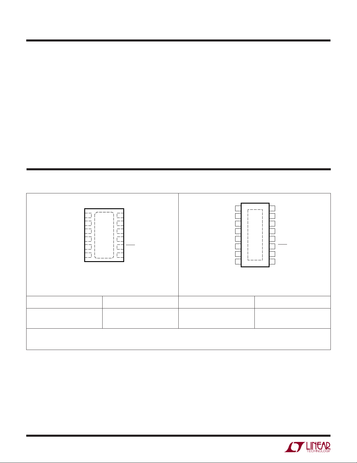
TOP VIEW
NC
1
OUT
2
OUT
3
ADJ
4
GND
5
PWRGD
T
6
12-LEAD (4mm × 3mm) PLASTIC DFN
JMAX
DE PACKAGE
= 125°C, θJA = 40°C/W, θJC = 16°C/W
EXPOSED PAD (PIN 13) IS GND
MUST BE SOLDERED TO PCB
12
11
10
13
9
8
7
NC
IN
IN
NC
SHDN
C
T
GND
NC
OUT
OUT
ADJ
GND
PWRGD
GND
T
JMAX
TOP VIEW
1
2
3
4
17
5
6
7
8
FE PACKAGE
16-LEAD PLASTIC TSSOP
= 140°C, θJA = 40°C/W, θJC = 16°C/W
EXPOSED PAD (PIN 17) IS GND
MUST BE SOLDERED TO PCB
GND
16
NC
15
IN
14
IN
13
NC
12
SHDN
11
C
10
T
GND
9
ORDER PART NUMBER DE PART MARKING ORDER PART NUMBER FE PART MARKING*
LT3013EDE 3013 LT3013EFE
LT3013HFE
Order Options Tape and Reel: Add #TR
Lead Free: Add #PBF Lead Free Tape and Reel: Add #TRPBF
Lead Free Part Marking: http://www.linear.com/leadfree/
Consult LTC Marketing for parts specifi ed with wider operating temperature ranges. *The temperature grade is identifi ed by a label on the shipping container.
3013EFE
3013HFE
2
3013fc
LT3013
ELECTRICAL CHARACTERISTICS
The ●
denotes the specifi cations which apply over the –40°C to 125°C operating temperature range, otherwise specifi cations are at TJ = 25°C.
(LT3013E)
PARAMETER CONDITIONS MIN TYP MAX UNITS
Minimum Input Voltage I
LOAD
ADJ Pin Voltage (Notes 2,3) V
4.75V < V
Line Regulation ΔV
Load Regulation (Note 2) V
V
Dropout Voltage
V
= V
IN
OUT(NOMINAL)
GND Pin Current
V
= 4.75V
IN
(Notes 4, 6)
(Notes 4, 5)
I
LOAD
I
LOAD
I
LOAD
I
LOAD
I
LOAD
I
LOAD
I
LOAD
I
LOAD
I
LOAD
Output Voltage Noise C
= 250mA
= 4V, I
IN
IN
= 4V to 80V, I
IN
= 4.75V, ΔI
IN
= 4.75V, ΔI
IN
= 10mA
= 10mA
= 50mA
= 50mA
= 250mA
= 250mA
= 0mA
= 100mA
= 250mA
= 10μF, I
OUT
= 1mA
LOAD
< 80V, 1mA < I
LOAD
= 1mA to 250mA
LOAD
= 1mA to 250mA
LOAD
= 250mA, BW = 10Hz to 100kHz 100 μV
LOAD
< 250mA
LOAD
= 1mA (Note 2)
●
1.225
●
1.2
●
4 4.75 V
1.24
1.24
1.255
1.28
0.1 5 mV
71225mV
●
160 230
●
300
250 340
●
420
400 490
●
●
65
620
120
3
●
10
18
RMS
ADJ Pin Bias Current (Note 7 ) 30 100 nA
Shutdown Threshold V
⎯S⎯H⎯D⎯
N Pin Current (Note 8) V
Quiescent Current in Shutdown V
= Off to On
OUT
V
= On to Off
OUT
⎯S⎯H⎯D⎯
N
V
⎯S⎯H⎯D⎯
N
= 6V, V
IN
= 0V
= 6V
= 0V 1 5 μA
⎯S⎯H⎯D⎯
N
PWRGD Trip Point % of Nominal Output Voltage, Output Rising
●
●
0.3
1.3
0.8
0.3
0.1
●
85 90 94 %
2V
2
1
PWRGD Trip Point Hysteresis % of Nominal Output Voltage 1.1 %
PWRGD Output Low Voltage I
C
Pin Charging Current 3.0 6 μA
T
C
Pin Voltage Differential V
T
Ripple Rejection V
Current Limit V
Reverse Output Current (Note 9) V
= 50μA
PWRGD
OUT
– V
RIPPLE
= 0V
OUT
CT(PWRGD Low)
= 0.5V
P-P
, f
RIPPLE
= –0.1V (Note 2)
= 120Hz, I
= 250mA 65 75 dB
LOAD
CT(PWRGD High)
= 7V(Avg), V
IN
= 7V, V
IN
V
= 4.75V, ΔV
IN
= 1.24V, VIN < 1.24V (Note 2) 12 25 μA
OUT
●
140 250 mV
1.6 V
400
●
250
V
V
mV
mV
mV
mV
mV
mV
mV
μA
mA
mA
V
μA
μA
ELECTRICAL CHARACTERISTICS
The ●
denotes the specifi cations which apply over the –40°C to 140°C operating temperature range, otherwise specifi cations are at TJ = 25°C.
(LT3013H)
PARAMETER CONDITIONS MIN TYP MAX UNITS
Minimum Input Voltage I
LOAD
ADJ Pin Voltage (Notes 2,3) V
4.75V < V
Line Regulation ΔV
Load Regulation (Note 2) V
V
= 200mA
= 4V, I
IN
IN
= 4V to 80V, I
IN
= 4.75V, ΔI
IN
= 4.75V, ΔI
IN
= 1mA
LOAD
< 80V, 1mA < I
LOAD
= 1mA to 200mA
LOAD
= 1mA to 200mA
LOAD
< 200mA
LOAD
= 1mA (Note 2)
●
1.225
●
1.2
●
4 4.75 V
1.24
1.24
1.255
1.28
0.1 5 mV
61230mV
●
3013fc
3
V
V
mV
LT3013
ELECTRICAL CHARACTERISTICS
The ●
denotes the specifi cations which apply over the –40°C to 140°C operating temperature range, otherwise specifi cations are at TJ = 25°C.
(LT3013H)
PARAMETER CONDITIONS MIN TYP MAX UNITS
Dropout Voltage
= V
V
IN
OUT(NOMINAL)
(Notes 4, 5)
GND Pin Current
V
= 4.75V
IN
(Notes 4, 6)
Output Voltage Noise C
I
LOAD
I
LOAD
I
LOAD
I
LOAD
I
LOAD
I
LOAD
I
LOAD
I
LOAD
I
LOAD
OUT
= 10mA
= 10mA
= 50mA
= 50mA
= 200mA
= 200mA
= 0mA
= 100mA
= 200mA
= 10μF, I
●
●
●
●
●
= 200mA, BW = 10Hz to 100kHz 100 μV
LOAD
160 230
320
250 340
450
360 490
630
65
130
3
7
18
RMS
ADJ Pin Bias Current (Note 7) 30 100 nA
Shutdown Threshold V
⎯S⎯H⎯D⎯
N Pin Current (Note 8) V
Quiescent Current in Shutdown V
= Off to On
OUT
V
= On to Off
OUT
⎯S⎯H⎯D⎯
N
V
⎯S⎯H⎯D⎯
N
= 6V, V
IN
= 0V
= 6V
= 0V 1 5 μA
⎯S⎯H⎯D⎯
N
PWRGD Trip Point % of Nominal Output Voltage, Output Rising
●
●
0.3
1.3
0.8
0.3
0.1
●
85 90 95 %
2V
2
1
PWRGD Trip Point Hysteresis % of Nominal Output Voltage 1.1 %
PWRGD Output Low Voltage I
C
Pin Charging Current 3.0 6 μA
T
C
Pin Voltage Differential V
T
Ripple Rejection V
Current Limit V
Reverse Output Current (Note 9) V
Note 1: Stresses beyond those listed under Absolute Maximum Ratings
may cause permanent damage to the device. Exposure to any Absolute
Maximum Rating condition for extended periods may affect device
reliability and lifetime.
Note 2: The LT3013 is tested and specifi ed for these conditions with the
ADJ pin connected to the OUT pin.
Note 3: Operating conditions are limited by maximum junction
temperature. The regulated output voltage specifi cation will not apply
for all possible combinations of input voltage and output current. When
operating at maximum input voltage, the output current range must be
limited. When operating at maximum output current, the input voltage
range must be limited.
Note 4: To satisfy requirements for minimum input voltage, the LT3013 is
tested and specifi ed for these conditions with an external resistor divider
(249k bottom, 649k top) for an output voltage of 4.5V. The external
resistor divider will add a 5μA DC load on the output.
Note 5: Dropout voltage is the minimum input to output voltage differential
needed to maintain regulation at a specifi ed output current. In dropout, the
output voltage will be equal to (V
– V
IN
= 50μA
PWRGD
OUT
– V
RIPPLE
= 0V
OUT
CT(PWRGD Low)
= 0.5V
P-P
, f
RIPPLE
= –0.1V (Note 2)
= 120Hz, I
= 200mA 65 75 dB
LOAD
CT(PWRGD High)
= 7V(Avg), V
IN
= 7V, V
IN
V
= 4.75V, ΔV
IN
= 1.24V, VIN < 1.24V (Note 2) 12 25 μA
OUT
Note 6: GND pin current is tested with V
load. This means the device is tested while operating close to its dropout
region. This is the worst-case GND pin current. The GND pin current will
decrease slightly at higher input voltages.
Note 7: ADJ pin bias current fl ows into the ADJ pin.
⎯S⎯H⎯D⎯
Note 8:
N pin current fl ows out of the ⎯S⎯H⎯D⎯N pin.
Note 9: Reverse output current is tested with the IN pin grounded and the
OUT pin forced to the rated output voltage. This current fl ows into the OUT
pin and out the GND pin.
Note 10: The LT3013E is guaranteed to meet performance specifi cations
from 0°C to 125°C operating junction temperature. Specifi cations over
the –40°C to 125°C operating junction temperature range are assured by
design, characterization and correlation with statistical process controls.
The LT3013H is tested to the LT3013H Electrical Characteristics table at
140°C operating junction temperature. High junction temperatures degrade
operating lifetimes. Operating lifetime is derated at junction temperatures
greater than 125°C.
DROPOUT
).
Note 11: This IC includes overtemperature protection that is intended
to protect the device during momentary overload conditions. Junction
●
140 250 mV
1.6 V
400 mA
●
200
= 4.75V and a current source
IN
temperature will exceed 125°C (LT3013E) or 140°C (LT3013H) when
overtemperature protection is active. Continuous operation above the
specifi ed maximum operating junction temperature may impair device
reliability.
3013fc
mV
mV
mV
mV
mV
mV
μA
mA
mA
V
μA
μA
mA
4
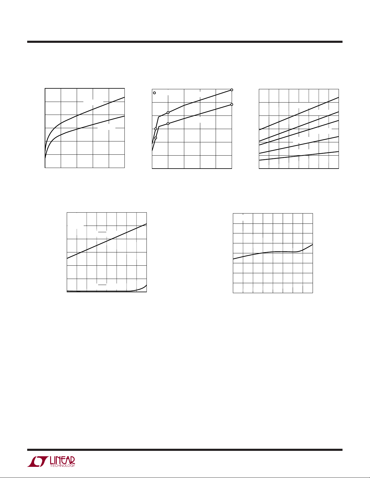
TYPICAL PERFORMANCE CHARACTERISTICS
Typical Dropout Voltage Guaranteed Dropout Voltage Dropout Voltage
600
500
400
300
200
DROPOUT VOLTAGE (mV)
100
0
0
OUTPUT CURRENT (mA)
Quiescent Current ADJ Pin Voltage
120
VIN = 6V
R
L
= 0
I
100
L
80
60
40
QUIESCENT CURRENT (µA)
20
0
–50 0
TJ = 125°C
10050
= ∞
–25
TJ = 25°C
200150
3013 G01
V
= V
SHDN
IN
V
= GND
SHDN
50
25
TEMPERATURE (°C)
75
250
600
= TEST POINTS
500
400
300
200
100
GUARANTEED DROPOUT VOLTAGE (mV)
0
100
150125
3013 G04
TJ ≤ 125°C
TJ ≤ 25°C
100 200
OUTPUT CURRENT (mA)
250500 150
3013 G02
1.260
1.255
1.250
1.245
1.240
1.235
ADJ PIN VOLTAGE (V)
1.230
1.225
1.220
–50 0
600
500
400
300
200
DROPOUT VOLTAGE (mV)
100
0
–50 0
IL = 1mA
–25
TEMPERATURE (°C)
LT3013
IL = 250mA
IL = 100mA
IL = 50mA
IL = 10mA
IL = 1mA
50
–25
25
25
TEMPERATURE (°C)
50
75
100
75
3013 G05
100
150125
150125
3013 G03
3013fc
5
LT3013
TYPICAL PERFORMANCE CHARACTERISTICS
Quiescent Current
80
TJ = 25°C
= ∞
R
L
70
60
50
40
30
20
QUIESCENT CURRENT (µA)
10
0
21
0
10
GND PIN CURRENT (mA)
V
= V
SHDN
V
= GND
SHDN
67 9
43
5
INPUT VOLTAGE (V)
GND Pin Current
TJ = 25°C, *FOR V
9
8
7
6
5
4
3
2
1
0
21
0
INPUT VOLTAGE (V)
IN
8
10
3013 G06
= 1.24V
OUT
RL = 4.96Ω
= 250mA*
I
L
RL = 12.4Ω
= 100mA*
I
L
RL = 24.8Ω, IL = 50mA*
67 9
43
5
8
Quiescent Current
250
TJ = 25°C
=
R
225
L
V
OUT
200
175
150
125
100
75
QUIESCENT CURRENT (µA)
50
25
0
0
10
3013 G08
∞
= 1.24V
V
SHDN
2010
INPUT VOLTAGE (V)
= V
GND Pin Current
1.2
1.0
0.8
IN
V
= GND
SHDN
4030
60 70
50
80
3013 G06b
0.6
0.4
GND PIN CURRENT (mA)
0.2
0
0
GND Pin Current vs I
10
VIN = 4.75V
9
= 25°C
T
J
8
7
6
5
4
3
GND PIN CURRENT (mA)
2
1
0
0
10050
LOAD CURRENT (mA)
RL = 49.6Ω
I
21
INPUT VOLTAGE (V)
LOAD
= 25mA*
L
RL = 1.24k
I
L
43
200150
TJ = 25°C
*FOR V
OUT
RL = 124Ω
I
= 1mA*
67 9
5
250
3013 G09
= 1.24V
= 10mA*
L
8
10
3013 G07
6
3013fc

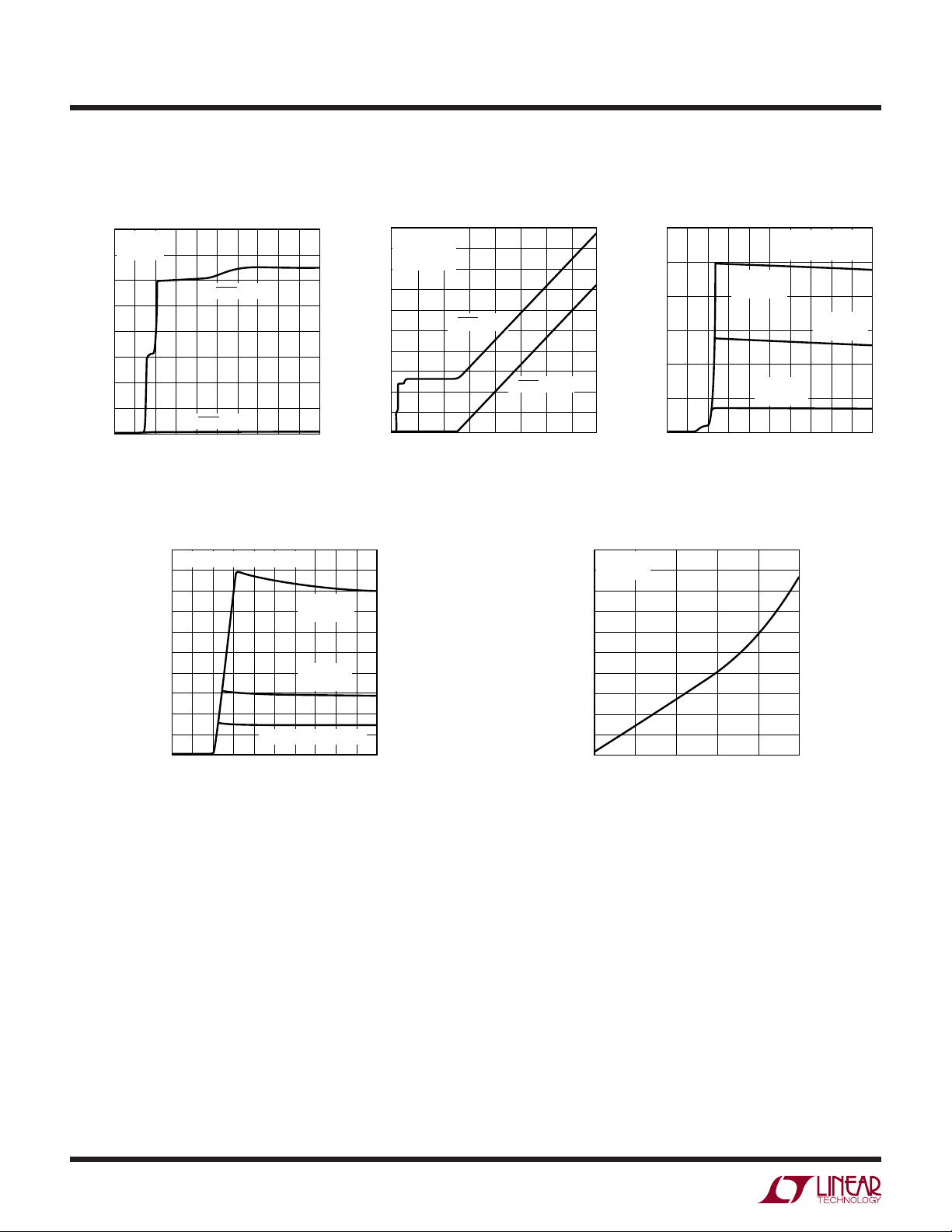
TYPICAL PERFORMANCE CHARACTERISTICS
LT3013
⎯S⎯H⎯D⎯
N Pin Threshold
2.0
1.8
1.6
1.4
1.2
1.0
0.8
0.6
SHDN PIN THRESHOLD (V)
0.4
0.2
0
–50 0
–25
ON-TO-OFF
25
TEMPERATURE (°C)
ADJ Pin Bias Current
120
100
80
60
40
ADJ PIN BIAS CURRENT (nA)
20
0
–50 0
OFF-TO-ON
50
–25
75
100
3013 G10
50
25
TEMPERATURE (°C)
75
0.6
0.5
0.4
0.3
0.2
SHDN PIN CURRENT (µA)
0.1
0
–50 0
⎯S⎯H⎯D⎯
N Pin Current
VIN = 6V
= 0V
V
SHDN
CURRENT FLOWS
OUT OF SHDN PIN
–25
25
TEMPERATURE (°C)
50
75
100
150125
3013 G12
⎯S⎯H⎯D⎯
N Pin Current
0.6
TJ = 25°C
CURRENT FLOWS
OUT OF SHDN PIN
0.5
0.4
0.3
0.2
SHDN PIN CURRENT (µA)
0.1
150125
0
1.0 2.0
SHDN PIN VOLTAGE (V)
3.00.50 1.5 2.5
3013 G11
PWRGD Trip Point
95
94
93
92
91
OUTPUT RISING
OUTPUT FALLING
50
25
TEMPERATURE (°C)
75
100
150125
3013 G25
100
3013 G13
90
89
88
87
86
PWRGD TRIP POINT (% OF OUTPUT VOLTAGE)
150125
85
–50 0
–25
3013fc
7

LT3013
TYPICAL PERFORMANCE CHARACTERISTICS
PWRGD Output Low Voltage
200
I
= 50µA
PWRGD
180
160
140
120
100
80
60
40
PWRGD OUTPUT LOW VOLTAGE (mV)
20
0
–50 0
–25
50
25
TEMPERATURE (°C)
75
Current Limit
1000
V
= 0V
OUT
900
800
700
600
500
400
300
CURRENT LIMIT (mA)
200
100
0
TJ = 125°C
0
2010
INPUT VOLTAGE (V)
100
TJ = 25°C
4030
3013 G26
50
150125
60 70
CT Charging Current
4.0
PWRGD TRIPPED HIGH
3.5
3.0
2.5
2.0
1.5
CHARGING CURRENT (µA)
1.0
T
C
0.5
0
–50 0
–25
80
3013 G14
50
25
TEMPERATURE (°C)
75
100
3013 G27
700
600
500
400
300
200
CURRENT LIMIT (mA)
100
COMPARATOR THRESHOLDS (V)
T
C
150125
Current Limit
VIN = 7V
= 0V
V
OUT
0
–50 0
–25
CT Comparator Thresholds
2.0
1.8
1.6
1.4
1.2
1.0
0.8
0.6
0.4
0.2
0
–50 0
–25
50
25
TEMPERATURE (°C)
VCT (HIGH)
VCT (LOW)
50
25
TEMPERATURE (°C)
75
100
75
3013 G15
100
150125
150125
3013 G28
8
3013fc

TYPICAL PERFORMANCE CHARACTERISTICS
LT3013
Reverse Output Current
200
TJ = 25°C
= 0V
V
180
IN
= V
V
OUT
160
140
120
100
80
60
40
REVERSE OUTPUT CURRENT (µA)
20
0
ADJ
CURRENT FLOWS
INTO OUTPUT PIN
21
0
OUTPUT VOLTAGE (V)
Input Ripple Rejection
100
VIN = 4.75V + 50mV
90
I
LOAD
80
70
60
50
40
30
RIPPLE REJECTION (dB)
20
10
0
10
ADJ
PIN CLAMP
(SEE APPLICATIONS
INFORMATION)
67 9
8
3013 G16
RIPPLE
C
C
OUT
10
OUT
= 3.3µF
= 10µF
3013 G19
43
5
= 250mA
100 1k 10k 100k 1M
RMS
FREQUENCY (Hz)
Reverse Output Current Input Ripple Rejection
120
100
80
60
40
20
REVERSE OUTPUT CURRENT (µA)
0
–50 0
VIN = 0V
= V
V
OUT
–25
= 1.24V
ADJ
50
25
TEMPERATURE (°C)
75
100
150125
3013 G17
92
88
84
80
76
72
RIPPLE REJECTION (dB)
68
VIN = 4.75V + 0.5V
64
= 250mA
I
L
= 1.24V
V
OUT
60
–50 0
–25
TEMPERATURE (°C)
Minimum Input Voltage
5.0
I
= 250mA
LOAD
4.5
4.0
3.5
3.0
2.5
2.0
1.5
1.0
MINIMUM INPUT VOLTAGE (V)
0.5
0
–50 0
–25
50
25
TEMPERATURE (°C)
75
RIPPLE AT f = 120Hz
P-P
50
25
100
75
150125
3013 G20
100
150125
3013 G18
3013fc
9

LT3013
0
k
TYPICAL PERFORMANCE CHARACTERISTICS
Load Regulation Output Noise Spectral Density
0
∆IL = 1mA TO 250mA
–2
–4
–6
–8
–10
–12
–14
LOAD REGULATION (mV)
–16
–18
–20
–50 0
–25
50
25
TEMPERATURE (°C)
75
100
150125
3013 G21
10
C
= 3.3µF
OUT
= 250mA
I
LOAD
1
0.1
OUTPUT NOISE SPECTRAL DENSITY (µV/√Hz)
0.01
10 1k 10k 100
100
FREQUENCY (Hz)
3013 G22
V
OUT
100µV/DIV
10Hz to 100kHz Output Noise
C
OUT
= 250mA
I
L
V
OUT
= 10µF
= 1.24V
1ms/DIV
3013 G23
Transient Response
0.15
0.10
0.05
0
–0.05
DEVIATION (V)LOAD CURRENT (mA)
OUTPUT VOLTAGE
–0.10
–0.15
300
200
100
0
0
100
VIN = 6V
= 5V
V
OUT
= 3.3µF CERAMIC
C
IN
= 3.3µF CERAMIC
C
OUT
= 100mA TO 200mA
∆I
LOAD
300
200
TIME (µs)
400
50
3013 G24
10
3013fc

LT3013
PIN FUNCTIONS
NC (Pins 1, 9, 12)/(Pins 2, 12, 15): No Connect. These
pins have no internal connection; connecting NC pins to a
copper area for heat dissipation provides a small improvement in thermal performance.
OUT (Pins 2, 3)/(Pins 3, 4): Output. The output supplies
power to the load. A minimum output capacitor of 3.3μF
is required to prevent oscillations. Larger output capacitors will be required for applications with large transient
loads to limit peak voltage transients. See the Applications
Information section for more information on output capacitance and reverse output characteristics.
ADJ (Pin 4)/(Pin 5): Adjust. This is the input to the error
amplifi er. This pin is internally clamped to ±7V. It has a
bias current of 30nA which fl ows into the pin (see curve
of ADJ Pin Bias Current vs Temperature in the Typical
Performance Characteristics). The ADJ pin voltage is
1.24V referenced to ground, and the output voltage range
is 1.24V to 60V.
GND (Pins 5, 13)/(Pins 1, 6, 8, 9, 16, 17): Ground. The
exposed backside of the package is an electrical connection
for GND. As such, to ensure optimum device operation and
thermal performance, the exposed pad must be connected
directly to pin 5/pin 6 on the PC board.
PWRGD (Pin 6)/(Pin 7): Power Good. The PWRGD fl ag is
an open collector fl ag to indicate that the output voltage
has come up to above 90% of the nominal output voltage.
There is no internal pull-up on this pin; a pull-up resistor
must be used. The PWRGD pin will change state from an
open-collector to high impedance after both the output is
above 90% of the nominal voltage and the capacitor on
the CT pin has charged through a 1.6V differential. The
maximum pull-down current of the PWRGD pin in the
low state is 50μA.
(DFN Package)/(TSSOP Package)
⎯S⎯H⎯D⎯
N (Pin 8)/(Pin 11): Shutdown. The ⎯S⎯H⎯D⎯N pin is used
to put the LT3013 into a low power shutdown state. The
⎯S⎯H⎯D⎯
output will be off when the
⎯S⎯H⎯D⎯
N pin can be driven either by 5V logic or open-collector
logic with a pull-up resistor. The pull-up resistor is only
required to supply the pull-up current of the open-collector gate, normally several microamperes. If unused, the
⎯S⎯H⎯D⎯
N pin must be tied to a logic high or VIN.
(Pin 7)/(Pin 10): Timing Capacitor. The CT pin allows
C
T
the use of a small capacitor to delay the timing between
the point where the output crosses the PWRGD threshold and the PWRGD fl ag changes to a high impedance
state. Current out of this pin during the charging phase
is 3μA. The voltage difference between the PWRGD low
and PWRGD high states is 1.6V (see the Applications
Information Section).
IN (Pins 10, 11)/(Pins 13,14): Input. Power is supplied
to the device through the IN pin. A bypass capacitor is
required on this pin if the device is more than six inches
away from the main input fi lter capacitor. In general, the
output impedance of a battery rises with frequency, so it is
advisable to include a bypass capacitor in battery-powered
circuits. A bypass capacitor in the range of 1μF to 10μF
is suffi cient. The LT3013 is designed to withstand reverse
voltages on the IN pin with respect to ground and the OUT
pin. In the case of a reversed input, which can happen if
a battery is plugged in backwards, the LT3013 will act as
if there is a diode in series with its input. There will be no
reverse current fl ow into the LT3013 and no reverse voltage will appear at the load. The device will protect both
itself and the load.
N pin is pulled low. The
3013fc
11

LT3013
APPLICATIONS INFORMATION
The LT3013 is a 250mA high voltage low dropout regulator with micropower quiescent current and shutdown.
The device is capable of supplying 250mA at a dropout
voltage of 400mV. The low operating quiescent current
(65μA) drops to 1μA in shutdown. In addition to the
low quiescent current, the LT3013 incorporates several
protection features which make it ideal for use in battery-powered systems. The device is protected against
both reverse input and reverse output voltages. In battery
backup applications where the output can be held up by
a backup battery when the input is pulled to ground, the
LT3013 acts like it has a diode in series with its output
and prevents reverse current fl ow.
Adjustable Operation
The LT3013 has an output voltage range of 1.24V to 60V.
The output voltage is set by the ratio of two external
resistors as shown in Figure 1. The device servos the
output to maintain the voltage at the adjust pin at 1.24V
referenced to ground. The current in R1 is then equal to
1.24V/R1 and the current in R2 is the current in R1 plus
the ADJ pin bias current. The ADJ pin bias current, 30nA
at 25°C, fl ows through R2 into the ADJ pin. The output
voltage can be calculated using the formula in Figure 1. The
value of R1 should be less than 250k to minimize errors
in the output voltage caused by the ADJ pin bias current.
Note that in shutdown the output is turned off and the
divider current will be zero.
The adjustable device is tested and specifi ed with the
ADJ pin tied to the OUT pin and a 5μA DC load (unless
otherwise specifi ed) for an output voltage of 1.24V. Specifi cations for output voltages greater than 1.24V will be
proportional to the ratio of the desired output voltage to
1.24V; (V
/1.24V). For example, load regulation for an
OUT
output current change of 1mA to 250mA is –7mV typical at
= 1.24V. At V
V
OUT
= 12V, load regulation is:
OUT
(12V/1.24V) • (–7mV) = –68mV
Output Capacitance and Transient Response
The LT3013 is designed to be stable with a wide range of
output capacitors. The ESR of the output capacitor affects
stability, most notably with small capacitors. A minimum
output capacitor of 3.3μF with an ESR of 3Ω or less is
recommended to prevent oscillations. The LT3013 is a
micropower device and output transient response will be
a function of output capacitance. Larger values of output
capacitance decrease the peak deviations and provide
improved transient response for larger load current
changes. Bypass capacitors, used to decouple individual
components powered by the LT3013, will increase the
effective output capacitor value.
12
= 1.24V
V
OUT
V
= 1.24V
ADJ
= 30nA AT 25°C
I
ADJ
OUTPUT RANGE = 1.24V TO 60V
R2
+ (I
)(R2)1 +
ADJ
R1
IN
V
IN
Figure 1. Adjustable Operation
OUT
LT3013
ADJ
GND
V
+
R2
R1
OUT
3013 F01
3013fc

APPLICATIONS INFORMATION
LT3013
Extra consideration must be given to the use of ceramic
capacitors. Ceramic capacitors are manufactured with a
variety of dielectrics, each with different behavior across
temperature and applied voltage. The most common
dielectrics used are specifi ed with EIA temperature characteristic codes of Z5U, Y5V, X5R and X7R. The Z5U and
Y5V dielectrics are good for providing high capacitances
in a small package, but they tend to have strong voltage
and temperature coeffi cients as shown in Figures 2 and 3.
When used with a 5V regulator, a 16V 10μF Y5V capacitor
can exhibit an effective value as low as 1μF to 2μF for the
DC bias voltage applied and over the operating temperature range. The X5R and X7R dielectrics result in more
stable characteristics and are more suitable for use as the
output capacitor. The X7R type has better stability across
temperature, while the X5R is less expensive and is available in higher values. Care still must be exercised when
using X5R and X7R capacitors; the X5R and X7R codes
only specify operating temperature range and maximum
capacitance change over temperature. Capacitance change
due to DC bias with X5R and X7R capacitors is better than
Y5V and Z5U capacitors, but can still be signifi cant enough
to drop capacitor values below appropriate levels. Capacitor DC bias characteristics tend to improve as component
case size increases, but expected capacitance at operating
voltage should be verifi ed.
Voltage and temperature coeffi cients are not the only
sources of problems. Some ceramic capacitors have a
piezoelectric response. A piezoelectric device generates
voltage across its terminals due to mechanical stress, similar to the way a piezoelectric accelerometer or microphone
works. For a ceramic capacitor the stress can be induced
by vibrations in the system or thermal transients.
PWRGD Flag and Timing Capacitor Delay
The PWRGD fl ag is used to indicate that the ADJ pin voltage is within 10% of the regulated voltage. The PWRGD
pin is an open-collector output, capable of sinking 50μA
of current when the ADJ pin voltage is low. There is no
internal pull-up on the PWRGD pin; an external pull-up
resistor must be used. When the ADJ pin rises to within
10% of its fi nal reference value, a delay timer is started.
At the end of this delay, programmed by the value of the
capacitor on the C
pin, the PWRGD pin switches to a high
T
impedance and is pulled up to a logic level by an external
pull-up resistor.
To calculate the capacitor value on the C
pin, use the
T
following formula:
It
•
C
TIME
=
CT DELAY
VV
CT HIGH CT LOW
–
() ()
20
0
–20
–40
–60
CHANGE IN VALUE (%)
–80
–100
0
26
Figure 2. Ceramic Capacitor DC Bias Characteristics Figure 3. Ceramic Capacitor Temperature Characteristics
BOTH CAPACITORS ARE 16V,
1210 CASE SIZE, 10µF
X5R
Y5V
4
8
DC BIAS VOLTAGE (V)
10
14
12
16
3013 F02
40
20
0
–20
–40
–60
CHANGE IN VALUE (%)
–80
BOTH CAPACITORS ARE 16V,
1210 CASE SIZE, 10µF
–100
–50
–25 0
X5R
Y5V
50 100 125
25 75
TEMPERATURE (°C)
3013 F03
13
3013fc

LT3013
APPLICATIONS INFORMATION
Figure 4 shows a block diagram of the PWRGD circuit. At
startup, the timing capacitor is discharged and the PWRGD
pin will be held low. As the output voltage increases and
the ADJ pin crosses the 90% threshold, the JK fl ip-fl op
is reset, and the 3μA current source begins to charge the
timing capacitor. Once the voltage on the C
the V
CT(HIGH)
threshold (approximately 1.7V at 25°C), the
pin reaches
T
capacitor voltage is clamped and the PWRGD pin is set to
a high impedance state.
During normal operation, an internal glitch fi lter will ignore
short transients (<15μs). Longer transients below the 90%
threshold will reset the JK fl ip-fl op. This fl ip-fl op ensures
that the capacitor on the C
the way to the V
CT(LOW)
pin is quickly discharged all
T
threshold before re-starting the
time delay. This provides a consistent time delay after the
ADJ pin is within 10% of the regulated voltage before the
PWRGD pin switches to high impedance.
Thermal Considerations
The power handling capability of the device will be limited
by the maximum rated junction temperature (125°C for
LT3013E or 140°C for LT3013HFE). The power dissipated
by the device will be made up of two components:
1. Output current multiplied by the input/output voltage
differential: I
• (VIN – V
OUT
OUT
) and,
2. GND pin current multiplied by the input voltage:
GND
• VIN.
I
The GND pin current can be found by examining the GND
Pin Current curves in the Typical Performance Characteristics. Power dissipation will be equal to the sum of the
two components listed above.
The LT3013 has internal thermal limiting designed to protect the device during overload conditions. For continuous
normal conditions the maximum junction temperature
rating of 125°C (E-grade) or 140°C (H-grade)must not be
exceeded. It is important to give careful consideration to
all sources of thermal resistance from junction to ambient. Additional heat sources mounted nearby must also
be considered.
ADJ
V
REF
• 90%
3µA
I
CT
C
T
+
QJ
–
Figure 4. PWRGD Circuit Block Diagram
K
–
+
V
CT(LOW)
~0.1V
V
CT(HIGH)
(~1.1V)
– V
PWRGD
BE
3013 F04
3013fc
14

APPLICATIONS INFORMATION
LT3013
For surface mount devices, heat sinking is accomplished
by using the heat spreading capabilities of the PC board
and its copper traces. Copper board stiffeners and plated
through-holes can also be used to spread the heat generated by power devices.
The following tables list thermal resistance for several
different board sizes and copper areas. All measurements
were taken in still air on 3/32” FR-4 board with one ounce
copper.
Table 1. TSSOP Measured Thermal Resistance
COPPER AREA
TOPSIDE BOARD AREA
2500 sq mm 2500 sq mm 40°C/W
1000 sq mm 2500 sq mm 45°C/W
225 sq mm 2500 sq mm 50°C/W
100 sq mm 2500 sq mm 62°C/W
Table 2. DFN Measured Thermal Resistance
COPPER AREA
TOPSIDE BOARD AREA
2500 sq mm 2500 sq mm 40°C/W
1000 sq mm 2500 sq mm 45°C/W
225 sq mm 2500 sq mm 50°C/W
100 sq mm 2500 sq mm 62°C/W
THERMAL RESISTANCE
(JUNCTION-TO-AMBIENT)
THERMAL RESISTANCE
(JUNCTION-TO-AMBIENT)
The thermal resistance junction-to-case (θJC), measured
at the exposed pad on the back of the die, is 16°C/W.
Continuous operation at large input/output voltage differentials and maximum load current is not practical
due to thermal limitations. Transient operation at high
input/output differentials is possible. The approximate
thermal time constant for a 2500sq mm 3/32” FR-4 board
with maximum topside and backside area for one ounce
copper is 3 seconds. This time constant will increase as
more thermal mass is added (i.e., vias, larger board, and
other components).
Calculating Junction Temperature
Example 1: Given an output voltage of 5V, an input voltage
range of 8V to 12V, an output current range of 0mA to
250mA, and a maximum ambient temperature of 30°C,
what will the maximum junction temperature be?
The power dissipated by the device will be equal to:
I
OUT(MAX)
• (V
IN(MAX)
– V
OUT
) + (I
GND
• V
IN(MAX)
)
where:
at (I
= 250mA
= 12V
= 250mA, VIN = 12V) = 8mA
OUT
I
OUT(MAX)
V
IN(MAX)
I
GND
So:
P = 250mA • (12V – 5V) + (8mA • 12V) = 1.85W
The thermal resistance will be in the range of 40°C/W to
62°C/W depending on the copper area. So the junction
temperature rise above ambient will be approximately
equal to:
1.85W • 50°C/W = 92.3°C
The maximum junction temperature will then be equal to
the maximum junction temperature rise above ambient
plus the maximum ambient temperature or:
T
= 30°C + 92.3°C = 122.3°C
JMAX
Example 2: Given an output voltage of 5V, an input voltage
of 48V that rises to 72V for 5ms(max) out of every 100ms,
and a 5mA load that steps to 200mA for 50ms out of every 250ms, what is the junction temperature rise above
ambient? Using a 500ms period (well under the time
constant of the board), power dissipation is as follows:
P1(48V in, 5mA load) = 5mA • (48V – 5V)
+ (200μA • 48V) = 0.23W
For an application with transient high power peaks, average
power dissipation can be used for junction temperature
calculations if the pulse period is signifi cantly less than
the thermal time constant of the device and board.
P2(48V in, 50mA load) = 200mA • (48V – 5V)
+ (8mA • 48V) = 8.98W
P3(72V in, 5mA load) = 5mA • (72V – 5V)
+ (200μA • 72V) = 0.35W
P4(72V in, 50mA load) = 200mA • (72V – 5V)
+ (8mA • 72V) = 13.98W
3013fc
15

LT3013
APPLICATIONS INFORMATION
Operation at the different power levels is as follows:
76% operation at P1, 19% for P2, 4% for P3, and
1% for P4.
P
+ 1%(13.98W) = 2.03W
With a thermal resistance in the range of 40°C/W to
62°C/W, this translates to a junction temperature rise
above ambient of 81°C to 125°C.
High Temperature Operation
Care must be taken when designing LT3013 applications to
operate at high ambient temperatures. The LT3013 works
at elevated temperatures but erratic operation can occur
due to unforeseen variations in external components. Some
tantalum capacitors are available for high temperature
operation, but ESR is often several ohms; capacitor ESR
above 3Ω is unsuitable for use with the LT3013. Ceramic
capacitor manufacturers (Murata, AVX, TDK, and Vishay
Vitramon at this writing) now offer ceramic capacitors that
are rated to 150°C using an X8R dielectric. Device instability
will occur if output capacitor value and ESR are outside
design limits at elevated temperature and operating DC
voltage bias (see information on capacitor characteristics
under Output Capacitance and Transient Response). Check
each passive component for absolute value and voltage
ratings over the operating temperature range.
Leakages in capacitors or from solder fl ux left after insuffi cient board cleaning adversely affects low quiescent
current operation. The output voltage resistor divider
should use a maximum bottom resistor value of 124k to
compensate for high temperature leakage, setting divider
current to 10μA. Consider junction temperature increase
due to power dissipation in both the junction and nearby
components to ensure maximum specifi cations are not
violated for the device or external components.
= 76%(0.23W) + 19%(8.98W) + 4%(0.35W)
EFF
Protection Features
The LT3013 incorporates several protection features which
make it ideal for use in battery-powered circuits. In addition to the normal protection features associated with
monolithic regulators, such as current limiting and thermal
limiting, the device is protected against reverse-input voltages, and reverse voltages from output to input.
Current limit protection and thermal overload protection
are intended to protect the device against current overload
conditions at the output of the device. For normal operation, the junction temperature should not exceed 125°C
(LT3013E) or 140°C (LT3013HFE).
Like many IC power regulators, the LT3013 has safe operating area protection. The safe area protection decreases
the current limit as input voltage increases and keeps
the power transistor inside a safe operating region for
all values of input voltage. The protection is designed to
provide some output current at all values of input voltage
up to the device breakdown. The SOA protection circuitry
for the LT3013 uses a current generated when the input
voltage exceeds 25V to decrease current limit. This current shows up as additional quiescent current for input
voltages above 25V. This increase in quiescent current
occurs both in normal operation and in shutdown (see
curve of Quiescent Current in the Typical Performance
Characteristics).
The input of the device will withstand reverse voltages of
80V. No negative voltage will appear at the output. The
device will protect both itself and the load. This provides
protection against batteries which can be plugged in
backward.
The ADJ pin of the device can be pulled above or below
ground by as much as 7V without damaging the device.
If the input is left open circuit or grounded, the ADJ pin
will act like an open circuit when pulled below ground,
and like a large resistor (typically 100k) in series with a
diode when pulled above ground. If the input is powered
by a voltage source, pulling the ADJ pin below the reference voltage will cause the device to current limit. This
will cause the output to go to a unregulated high voltage.
Pulling the ADJ pin above the reference voltage will turn
off all output current.
16
3013fc

APPLICATIONS INFORMATION
LT3013
In situations where the ADJ pin is connected to a resistor
divider that would pull the ADJ pin above its 7V clamp voltage if the output is pulled high, the ADJ pin input current
must be limited to less than 5mA. For example, a resistor
divider is used to provide a regulated 1.5V output from the
1.24V reference when the output is forced to 60V. The top
resistor of the resistor divider must be chosen to limit the
current into the ADJ pin to less than 5mA when the ADJ
pin is at 7V. The 53V difference between the OUT and ADJ
pins divided by the 5mA maximum current into the ADJ
pin yields a minimum top resistor value of 10.6k.
In circuits where a backup battery is required, several
different input/output conditions can occur. The output
voltage may be held up while the input is either pulled
to ground, pulled to some intermediate voltage, or is left
200
TJ = 25°C
= 0V
V
180
IN
= V
V
OUT
160
140
120
100
80
60
40
REVERSE OUTPUT CURRENT (µA)
20
0
ADJ
CURRENT FLOWS
INTO OUTPUT PIN
21
0
OUTPUT VOLTAGE (V)
43
open circuit. Current fl ow back into the output will follow
the curve shown in Figure 5. The rise in reverse output
current above 7V occurs from the breakdown of the 7V
clamp on the ADJ pin. With a resistor divider on the
regulator output, this current will be reduced depending
on the size of the resistor divider.
When the IN pin of the LT3013 is forced below the OUT
pin or the OUT pin is pulled above the IN pin, input current will typically drop to less than 2μA. This can happen
if the input of the LT3013 is connected to a discharged
(low voltage) battery and the output is held up by either
a backup battery or a second regulator circuit. The state
⎯S⎯H⎯D⎯
of the
N pin will have no effect on the reverse output
current when the output is pulled above the input.
ADJ
PIN CLAMP
(SEE ABOVE)
67 9
8
5
10
3013 F05
Figure 5. Reverse Output Current
3013fc
17

LT3013
TYPICAL APPLICATIONS
5V Buck Converter with Low Current Keep Alive Backup
6
5.5V*
TO 60V
V
IN
C3
4.7µF
100V
CERAMIC
BOOST
4
V
IN
LT1766
15
SHDN
14
SYNC
GND
1, 8, 9, 16
SW
BIAS
V
2
10
12
FB
C
11
C
C
1nF
C2
0.33µF
D1
10MQ060N
L1
15µH
D1N914
†
R1
15.4k
R2
4.99k
D2
Buck Converter
Effi ciency vs Load Current
V
+
C1
100µF 10V
SOLID
TANTALUM
OUT
5V
1A/250mA
100
V
OUT
L = 68µH
90
80
70
EFFICIENCY (%)
60
= 5V
VIN = 10V
VIN = 42V
OPERATING
CURRENT
HIGH
LOW
100k
14
LT3013
11
SHDN
7
PWRGD
GND
1
V
12V
(LATER 42V)
OFF
(72V TRANSIENT)
OFF
3
OUTIN
5
ADJ
C
T
10
1000pF
*
FOR INPUT VOLTAGES BELOW 7.5V,
750k
SOME RESTRICTIONS MAY APPLY
†
INCREASE L1 TO 30µH FOR LOAD
CURRENTS ABOVE 0.6A AND TO
249k
60µH ABOVE 1A
3013 TA03
50
0.25
0
0.75
0.50
LOAD CURRENT (A)
1.00
1.25
3013 TA04
LT3013 Automotive Application
+
IN
ON
1µF
NO PROTECTION
DIODE NEEDED!
SHDN
LT3013
GND
OUTIN
ADJ
750k
249k
3.3µF
LOAD: CLOCK,
SECURITY SYSTEM
ETC
LT3013 Telecom Application
V
48V
ON
IN
1µF
SHDN
LT3013
GND
OUTIN
750k
ADJ
NO PROTECTION
DIODE NEEDED!
249k
3.3µF
LOAD:
SYSTEM MONITOR
ETC
3013 TA05
+
BACKUP
BATTERY
–
18
3013fc

PACKAGE DESCRIPTION
0.65 ±0.05
3.50 ±0.05
1.70 ±0.05
(2 SIDES)2.20 ±0.05
0.25 ± 0.05
RECOMMENDED SOLDER PAD PITCH AND DIMENSIONS
NOTE:
1. DRAWING PROPOSED TO BE A VARIATION OF VERSION
(WGED) IN JEDEC PACKAGE OUTLINE M0-229
2. DRAWING NOT TO SCALE
3. ALL DIMENSIONS ARE IN MILLIMETERS
3.30 ±0.05
(2 SIDES)
0.50
BSC
DE Package
12-Lead Plastic DFN (4mm × 3mm)
(Reference LTC DWG # 05-08-1695)
4.00 ±0.10
(2 SIDES)
PIN 1
TOP MARK
PACKAGE OUTLINE
(NOTE 6)
0.200 REF
4. DIMENSIONS OF EXPOSED PAD ON BOTTOM OF PACKAGE DO NOT INCLUDE
MOLD FLASH. MOLD FLASH, IF PRESENT, SHALL NOT EXCEED 0.15mm ON ANY SIDE
5. EXPOSED PAD SHALL BE SOLDER PLATED
6. SHADED AREA IS ONLY A REFERENCE FOR PIN 1 LOCATION
ON THE TOP AND BOTTOM OF PACKAGE
3.00 ±0.10
(2 SIDES)
0.75 ±0.05
R = 0.20
TYP
1.70 ± 0.10
(2 SIDES)
0.00 – 0.05
LT3013
R = 0.115
TYP
0.25 ± 0.05
3.30 ±0.10
(2 SIDES)
BOTTOM VIEW—EXPOSED PAD
0.50
BSC
127
16
0.38 ± 0.10
PIN 1
NOTCH
(UE12/DE12) DFN 0603
16-Lead Plastic TSSOP (4.4mm)
(Reference LTC DWG # 05-08-1663)
3.58
(.141)
6.60 ±0.10
4.50 ±0.10
RECOMMENDED SOLDER PAD LAYOUT
0.09 – 0.20
(.0035 – .0079)
NOTE:
1. CONTROLLING DIMENSION: MILLIMETERS
2. DIMENSIONS ARE IN
3. DRAWING NOT TO SCALE
SEE NOTE 4
0.65 BSC
4.30 – 4.50*
(.169 – .177)
0.50 – 0.75
(.020 – .030)
MILLIMETERS
(INCHES)
0.45 ±0.05
FE Package
Exposed Pad Variation BB
4.90 – 5.10*
(.193 – .201)
16 1514 13 12 11
2.94
(.116)
1.05 ±0.10
1345678
2
0.25
REF
0° – 8°
0.65
(.0256)
BSC
0.195 – 0.30
(.0077 – .0118)
4. RECOMMENDED MINIMUM PCB METAL SIZE
FOR EXPOSED PAD ATTACHMENT
*DIMENSIONS DO NOT INCLUDE MOLD FLASH. MOLD FLASH
SHALL NOT EXCEED 0.150mm (.006") PER SIDE
TYP
3.58
(.141)
10 9
2.94
(.116)
1.10
(.0433)
MAX
0.05 – 0.15
(.002 – .006)
FE16 (BB) TSSOP 0204
6.40
(.252)
BSC
Information furnished by Linear Technology Corporation is believed to be accurate and reliable.
However, no responsibility is assumed for its use. Linear Technology Corporation makes no representation that the interconnection of its circuits as described herein will not infringe on existing patent rights.
3013fc
19

LT3013
TYPICAL APPLICATION
Constant Brightness for Indicator LED over Wide Input Voltage Range
–48V CAN VARY
FROM –4V TO –80V
RETURN
OFF
–48V
ON
I
= 1.24V/R
LED
1µF
IN
LT3013
SHDN
GND
SET
RELATED PARTS
PART NUMBER DESCRIPTION COMMENTS
LT1020 125mA, Micropower Regulator and Comparator V
LT1120/LT1120A 125mA, Micropower Regulator and Comparator V
LT1121/LT1121HV 150mA, Micropower, LDO V
LT1129 700mA, Micropower, LDO V
LT1676 60V, 440mA (I
), 100kHz, High Effi ciency
OUT
Step-Down DC/DC Converter
LT1761 100mA, Low Noise Micropower, LDO V
LT1762 150mA, Low Noise Micropower, LDO V
LT1763 500mA, Low Noise Micropower, LDO V
LT1764/LT1764A 3A, Low Noise, Fast Transient Response, LDO V
LT1766 60V, 1.2A (I
), 200kHz, High Effi ciency
OUT
Step-Down DC/DC Converter
LT1776 40V, 550mA (I
), 200kHz, High Effi ciency
OUT
Step-Down DC/DC Converter
LT1934/LT1934-1 300mA/60mA, (I
), Constant Off-Time, High
OUT
Effi ciency Step-Down DC/DC Converter
LT1956 60V, 1.2A (I
), 500kHz, High Effi ciency
OUT
Step-Down DC/DC Converter
LT1962 300mA, Low Noise Micropower, LDO V
LT1963/LT1963A 1.5A, Low Noise, Fast Transient Response, LDO V
LT1964 200mA, Low Noise Micropower, Negative LDO V
LT3010/LT3010H 50mA, 3V to 80V, Low Noise Micropower LDO V
LT3012/LT3012H 250mA, 4V to 80V, Low Dropout Micropower
Linear Regulator
LT3014/HV 20mA, 3V to 80V, Low Dropout Micropower
Linear Regulator
ThinSOT is a trademark of Linear Technology Corporation.
Linear Technology Corporation
20
1630 McCarthy Blvd., Milpitas, CA 95035-7417
(408) 432-1900 ● FAX: (408) 434-0507
●
www.linear.com
: 4.5V to 36V, V
IN
Comparator and Reference, Class B Outputs, S16, PDIP14 Packages
: 4.5V to 36V, V
IN
Comparator and Reference, Logic Shutdown, Ref Sources and Sinks 2/4mA,
S8, N8 Packages
: 4.2V to 30/36V, V
IN
Reverse Battery Protection, SOT-223, S8, Z Packages
: 4.2V to 30V, V
IN
DD, S0T-223, S8,TO220-5, TSSOP20 Packages
VIN: 7.4V to 60V, V
: 1.8V to 20V, V
IN
Low Noise < 20μV
: 1.8V to 20V, V
IN
Low Noise < 20μV
: 1.8V to 20V, V
IN
Low Noise < 20μV
: 2.7V to 20V, V
IN
Low Noise < 40μV
DD, TO220-5 Packages
VIN: 5.5V to 60V, V
VIN: 7.4V to 40V, V
90% Effi ciency, VIN: 3.2V to 34V, V
ThinSOT Package
VIN: 5.5V to 60V, V
: 1.8V to 20V, V
IN
Low Noise < 20μV
: 2.1V to 20V, V
IN
Low Noise < 40μV
DD, TO220-5, S0T-223, S8 Packages
: –1.9V to –20V, V
IN
Low Noise < 30μVRMS, Stable with Ceramic Capacitors, ThinSOT Package
: 3V to 8V, V
IN
Low Noise < 100μV
VIN: 4V to 80V, V
TSSOP-16E and 4mm × 3mm DFN-12 Packages, H Grade = +140°C T
VIN: 3V to 80V (100V for 2ms, HV version), V
I
= 7μA, ISD = <1μA, ThinSOT and 3mm × 3mm DFN-8 Packages
Q
OUT
ADJ
R
SET
OUT(MIN)
OUT(MIN)
OUT(MIN)
OUT(MIN)
OUT(MIN)
OUT(MIN)
, Stable with 1μF Ceramic Capacitors, ThinSOTTM Package
RMS
OUT(MIN)
, MS8 Package
RMS
OUT(MIN)
, S8 Package
RMS
OUT(MIN)
, “A” Version Stable with Ceramic Capacitors,
RMS
OUT(MIN)
OUT(MIN)
OUT(MIN)
OUT(MIN)
, MS8 Package
RMS
OUT(MIN)
, “A” Version Stable with Ceramic Capacitors,
RMS
OUT(MIN)
= 1.275V, VDO = 0.3V, IQ = 30μA, ISD = 1μA,
OUT(MIN)
, MS8E Package, H Grade = +140°C T
RMS
: 1.24V to 60V, VDO = 0.4V, IQ = 40μA, ISD = <1μA,
OUT
3.3µF
3013 TA06
= 2.5V, VDO = 0.4V, IQ = 40μA, ISD = 40μA,
= 2.5V, VDO = 0.4V, IQ = 40μA, ISD = 10μA,
= 3.75V, VDO = 0.42V, IQ = 30μA, ISD = 16μA,
= 3.75V, VDO = 0.4V, IQ = 50μA, ISD = 16μA,
= 1.24V, IQ = 3.2mA, ISD = 2.5μA, S8 Package
= 1.22V, VDO = 0.3V, IQ = 20μA, ISD = <1μA,
= 1.22V, VDO = 0.3V, IQ = 25μA, ISD = <1μA,
= 1.22V, VDO = 0.3V, IQ = 30μA, ISD = <1μA,
= 1.21V, VDO = 0.34V, IQ = 1mA, ISD = <1μA,
= 1.2V, IQ = 2.5mA, ISD = 25μA, TSSOP16/E Package
= 1.24V, IQ = 3.2mA, ISD = 30μA, N8, S8 Packages
= 1.25V, IQ = 14μA, ISD = <1μA,
OUT(MIN)
= 1.2V, IQ = 2.5mA, ISD = 25μA, TSSOP16/E Package
= 1.22V, VDO = 0.27V, IQ = 30μA, ISD = <1μA,
= 1.21V, VDO = 0.34V, IQ = 1mA, ISD = <1μA,
= –1.21V, VDO = 0.34V, IQ = 30μA, ISD = 3μA,
: 1.22V to 60V, VDO = 0.35V,
OUT
© LINEAR TECHNOLOGY CORPORATION 2005
JMAX
JMAX
3013fc
LT 0307 REV C • PRINTED IN USA
 Loading...