

Page 1
LP141WX5
Liquid Crystal Display
Product Specification
SPECIFICATION
FOR
APPROVAL
Preliminary Specification
)
(
)
(
Final Specification
●
14.1” WXGA TFT LCDTitle
MODEL
LenovoCustomer
*When you obtain standard approval,
please use the above model name without suffix
SIGNATUREAPPROVED BY
/
/
/
APPROVED BY
J. L. Ma / G. Manager
REVIEWED BY
Wyatt Park / Manager
PREPARED BY
S. S. Han / Engineer
K. M. Lee / Engineer
LG Display Co., Ltd.SUPPLIER
LP141WX5*MODEL
TLD1Suffix
SIGNATURE
Please return 1 copy for your confirmation with
your signature and comments.
Ver. 1.0 Aug. 15, 2008
Products Engineering Dept.
LG Display Co., Ltd
1 / 32
Page 2
Product Specification
Contents
LP141WX5
Liquid Crystal Display
COVER
CONTENTS
RECORD OF REVISIONS
GENERAL DESCRIPTION1
ABSOLUTE MAXIMUM RATINGS2
ELECTRICAL SPECIFICATIONS3
ELECTRICAL CHARACTREISTICS3-1
INTERFACE CONNECTIONS3-2
LVDS SIGNAL TIMING SPECIFICATIONS3-3
SIGNAL TIMING SPECIFICATIONS3-4
SIGNAL TIMING WAVEFORMS3-5
COLOR INPUT DATA REFERNECE3-6
POWER SEQUENCE3-7
OPTICAL SFECIFICATIONS4
ITEMNo
Page
1
2
3
4
5
6
7
9
11
11
12
13
14
MECHANICAL CHARACTERISTICS5
RELIABLITY6
INTERNATIONAL STANDARDS7
SAFETY7-1
EMC7-2
PACKING8
DESIGNATION OF LOT MARK8-1
PACKING FORM8-2
PRECAUTIONS9
APPENDIX. Enhanced Extended Display Identification Data A
Ver. 1.0 Aug. 15, 2008
18
25
26
26
27
27
28
30
2 / 32
Page 3
Product Specification
RECORD OF REVISIONS
LP141WX5
Liquid Crystal Display
30
DescriptionPageRevision DateRevision No
First Draft (Preliminary Specification)-May. 27. 20080.0
Update the Power Consumption4, 6Jul. 16. 20080.1
Update the Gray Scale15
Update the EDID Data30~32
Change the Power Consumption (B/L Power : 3.1W → 3.0W typ.)4Jul. 29. 20080.2
Update the Color Coordinates (R, G, B Color)14
Change the Label location in the mechanical drawing19~20
Change the EDID Data (Check sum : DA)
-. update the Color information (panel color coordinates part)
EDID
ver
-
0.1
0.2
1.0Final Specification-Aug. 15. 20081.0
Ver. 1.0 Aug. 15, 2008
3 / 32
Page 4
LP141WX5
Liquid Crystal Display
Product Specification
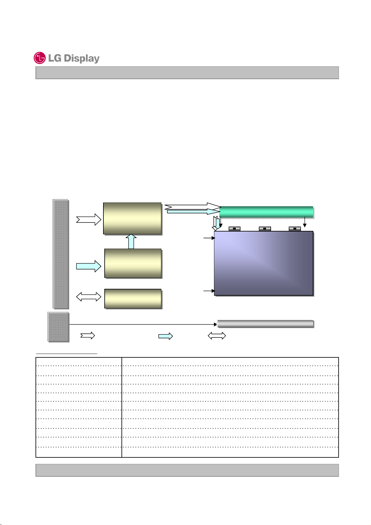
1. General Description
The LP141WX5 is a Color Active Matrix Liquid Crystal Display with an integral backlight system. The matrix
employs a-Si Thin Film Transistor as the active element. It is a transmissive type display operating in the
normally white mode. This TFT-LCD has 14.1 inches diagonally measured active display area with WXGA
resolution(800 vertical by 1280 horizontal pixel array). Each pixel is divided into Red, Green and Blue subpixels or dots which are arranged in vertical stripes. Gray scale or the brightness of the sub-pixel color is
determined with a 6-bit gray scale signal for each dot, thus, presenting a palette of more than 262,144
colors.
The LP141WX5 has been designed to apply the interface method that enables low power, high speed, low
EMI.
The LP141WX5 is intended to support applications where thin thickness, low power are critical factors and
graphic displays are important. In combination with the vertical arrangement of the sub-pixels, the
LP141WX5 characteristics provide an excellent flat display for office automation products such as Notebook
PC.
CN
CN
1
1
User connector
User connector
LVDS &
Timing
Control
Block
Source Driver Circuit
1
1
GIP(Gate In Panel)
1280
30
30
Pin
Pin
(
(
FPC
FPC
12
Pin)
12
Pin)
General Features
Outline Dimension
POWER
BLOCK
EDID
800
TFT-LCD Panel
(1280 x 800)
BLOCK
LED Backlight Ass’y
Control & Data Power EDID signal & Power
14.1 inches diagonal Active Screen Size
319.5(H,Typ.) × 205.5(V,Typ.) × 5.5(D,Max.) [mm]
0.2373mm × 0.2373 mmPixel Pitch
1280 horiz. By 800 vert. Pixels RGB strip arrangementPixel Format
6-bit, 262,144 colorsColor Depth
220 cd/m2(Typ.5 point)Luminance, White
Total 4.2 Watt(Typ.) @ LCM circuit 1.2 Watt (Typ._Mosaic), B/L 3.0Watt(Typ.)Power Consumption
360g(Max.)Weight
Transmissive mode, normally whiteDisplay Operating Mode
Glare treatment of the front polarizerSurface Treatment
YesRoHS Comply
Ver. 1.0 Aug. 15, 2008
4 / 32
Page 5
LP141WX5
Liquid Crystal Display
Product Specification
2. Absolute Maximum Ratings
The following are maximum values which, if exceeded, may cause faulty operation or damage to the unit.
Table 1. ABSOLUTE MAXIMUM RATINGS
Parameter Notes
Symbol
Values
Units
MaxMin
Power Input Voltage
Operating Temperature
Storage Temperature
Operating Ambient Humidity
Storage Humidity
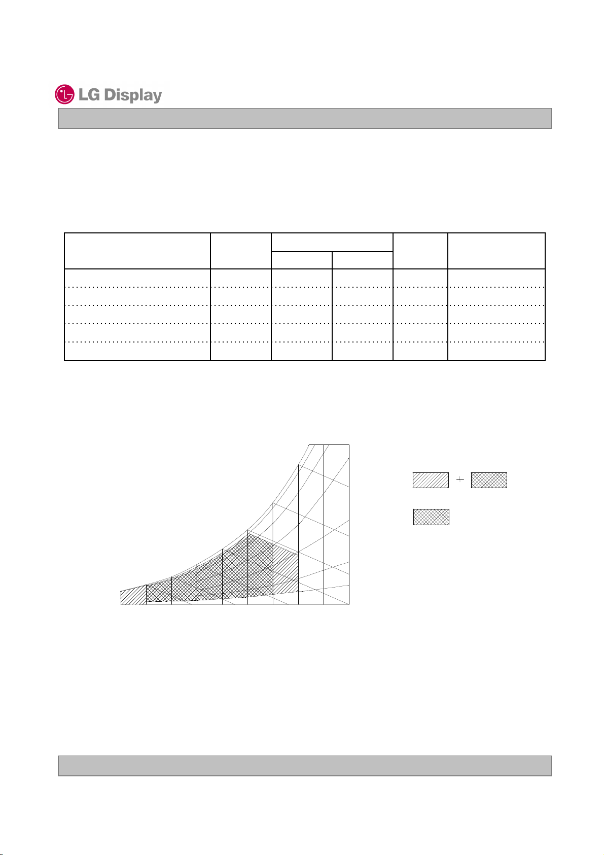
Note : 1. Temperature and relative humidity range are shown in the figure below.
Wet bulb temperature should be 39°C Max, and no condensation of water.
90% 80%
60%
Humidity[(%)RH]
Storage
40%
Operation
20%
10%
Wet Bulb
Temperature [℃℃℃℃]
20
10
0
60
50
40
30
at 25 ± 5°CVdc4.0-0.3VCC
1°C500TOP
1°C60-20HST
1%RH9010HOP
1%RH9010HST
-20
10
20 30 40 50
60 70 800
Dry Bulb Temperature [℃℃℃℃]
Ver. 1.0 Aug. 15, 2008
5 / 32
Page 6
LP141WX5
Liquid Crystal Display
Product Specification
3. Electrical Specifications
3-1. Electrical Characteristics
The LP141WX5 requires two power inputs. One is employed to power the LCD electronics and to drive the
TFT array and liquid crystal. The second input which powers the LED, is typically generated by an
inverter. The inverter is an external unit to the LCD.
Table 2. ELECTRICAL CHARACTERISTICS
Parameter Symbol
MODULE :
LED :
Operating Current
Operating Voltage per string
Power Consumption
I
CC
Mosaic
BL
LED
BL
Values
DC
V27.025.0V
RMS
NotesUnit
3V
1mA415360-Mosaic
1W1.41.2-PcPower Consumption
2Ohm11010090ZmDifferential Impedance
4mA
5W3.23.0-P
6Hrs10,000Life Time
MaxTypMin
3.63.33.0VCCPower Supply Input Voltage
21.020.05.0I
Note)
1. The specified current, voltage and power consumption are under the Vcc = 3.3V , 25℃, fv = 60Hz
condition whereas Mosaic pattern is displayed and fv is the frame frequency.
2. This impedance value is needed to proper display and measured form LVDS Tx to the mating connector.
3. The variance of the voltage is ± 10%.
4. The typical operating current is for the typical surface luminance (LWH) in optical characteristics.
I
is the current of each LEDs’ string, LED backlight has 6 strings on it.
LED
5. The LED power consumption shown above does not include power of external LED driver circuit
for typical current condition.
6. The life time is determined as the time at which brightness of LED is 50% compare to that of minimum
value specified in table 7.
Ver. 1.0 Aug. 15, 2008
6 / 32
Page 7
LP141WX5
Liquid Crystal Display
Product Specification
3-2. Interface Connections
This LCD employs two interface connections, a 30 pin connector is used for the module electronics interface
and the other connector is used for the integral backlight system.
The electronics interface connector is a model GT101-30S-HR11 manufactured by LSC.
Table 3. MODULE CONNECTOR PIN CONFIGURATION (CN1)
NotesDescriptionSymbolPin
GroundGND1
Power Supply, 3.3V Typ.VCC2
Power Supply, 3.3V Typ.VCC3
DDC 3.3V powerV EEDID4
Reserved for supplier test pointNC5
DDC ClockClk EEDID6
DDC DataDATA EEDID7
Negative LVDS differential data inputRIN0-8
Positive LVDS differential data inputRIN0+9
GroundGND10
Negative LVDS differential data inputRIN1-11
Positive LVDS differential data inputRIN1+12
GroundGND13
Negative LVDS differential data inputRIN2-14
Positive LVDS differential data inputRIN2+15
GroundGND16
Negative LVDS differential clock inputCLKIN-17
Positive LVDS differential clock inputCLKIN+18
GroundGND19
No ConnectNC20
NC No Connect21
GroundGND22
No ConnectNC23
No ConnectNC24
GroundGND25
No ConnectNC26
No ConnectNC27
GroundGND28
No ConnectNC29
No ConnectNC30
1, Interface chips
1.1 LCD : SW, SW0612B (LCD Controller)
including LVDS Receiver
1.2 System : THC63LVD823A or equivalent
* Pin to Pin compatible with LVDS
2. Connector
2.1 LCD : GT101-30S-HR11, LSC
2.2 Mating : FI-X30M or equivalent.
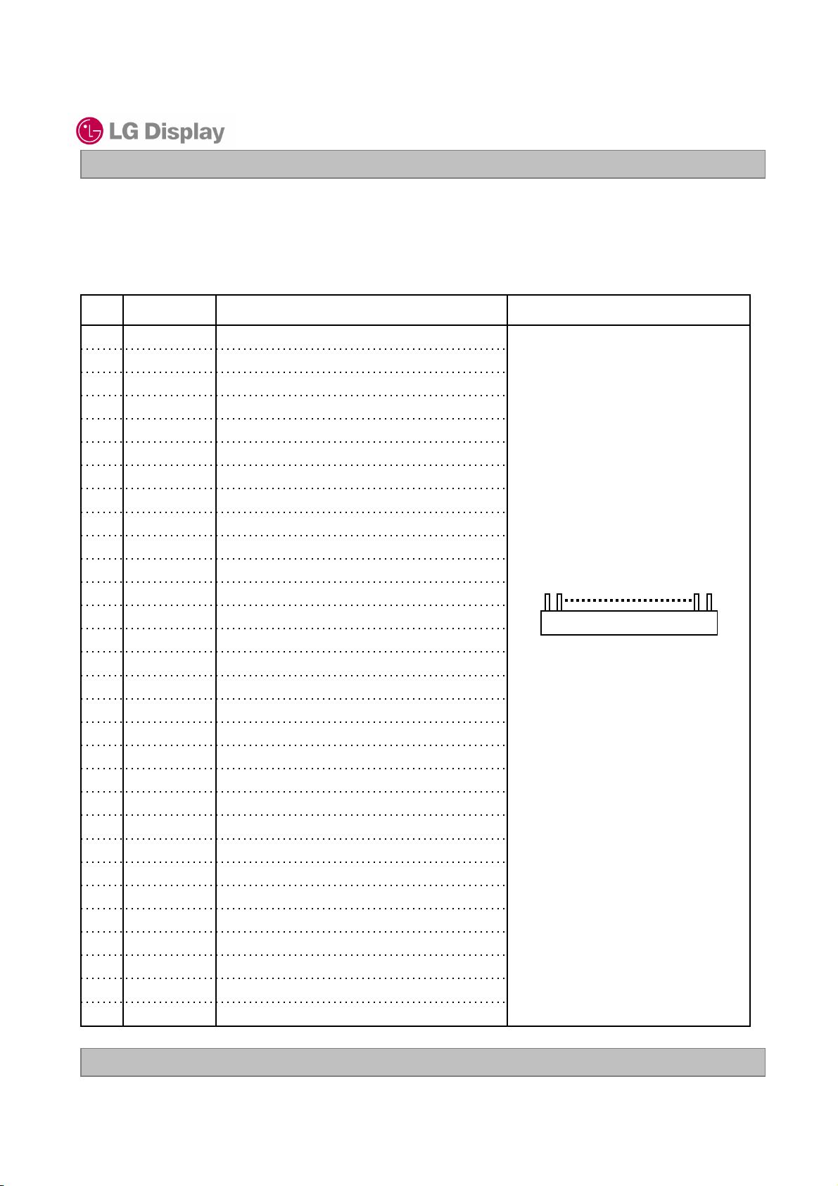
2.3 Connector pin arrangement
30
it’s compatible.
1
[LCD Module Rear View]
Ver. 1.0 Aug. 15, 2008
7 / 32
Page 8
Product Specification
Table 4. LED FPC CONNECTOR PIN CONFIGURATION
LP141WX5
Liquid Crystal Display
NotesDescriptionSymbolPin
LED Channel 1 CathodeFB11
LED Channel 2 CathodeFB22
LED Channel 3 CathodeFB33
LED Channel 4 CathodeFB44
LED Channel 5 CathodeFB55
LED Channel 6 CathodeFB66
No ConnectNC7
No ConnectNC8
No ConnectNC9
LED Power ( LED Anode)Vin10
LED Power ( LED Anode)Vin11
LED Power ( LED Anode)Vin12
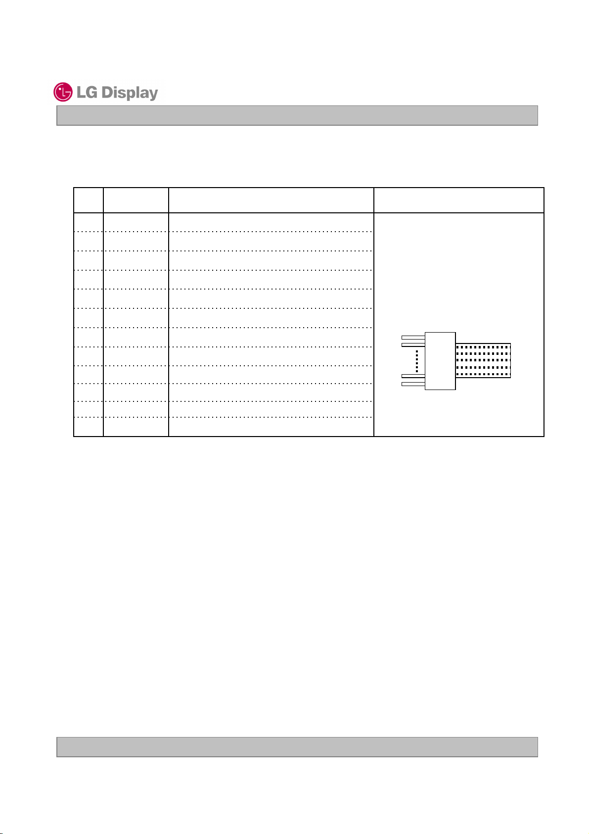
Connector
FH33-12S-0.5SH, Hirose
it’s compatible.
1
12
[LCD Module Front View]
FPC
Ver. 1.0 Aug. 15, 2008
8 / 32
Page 9
Product Specification
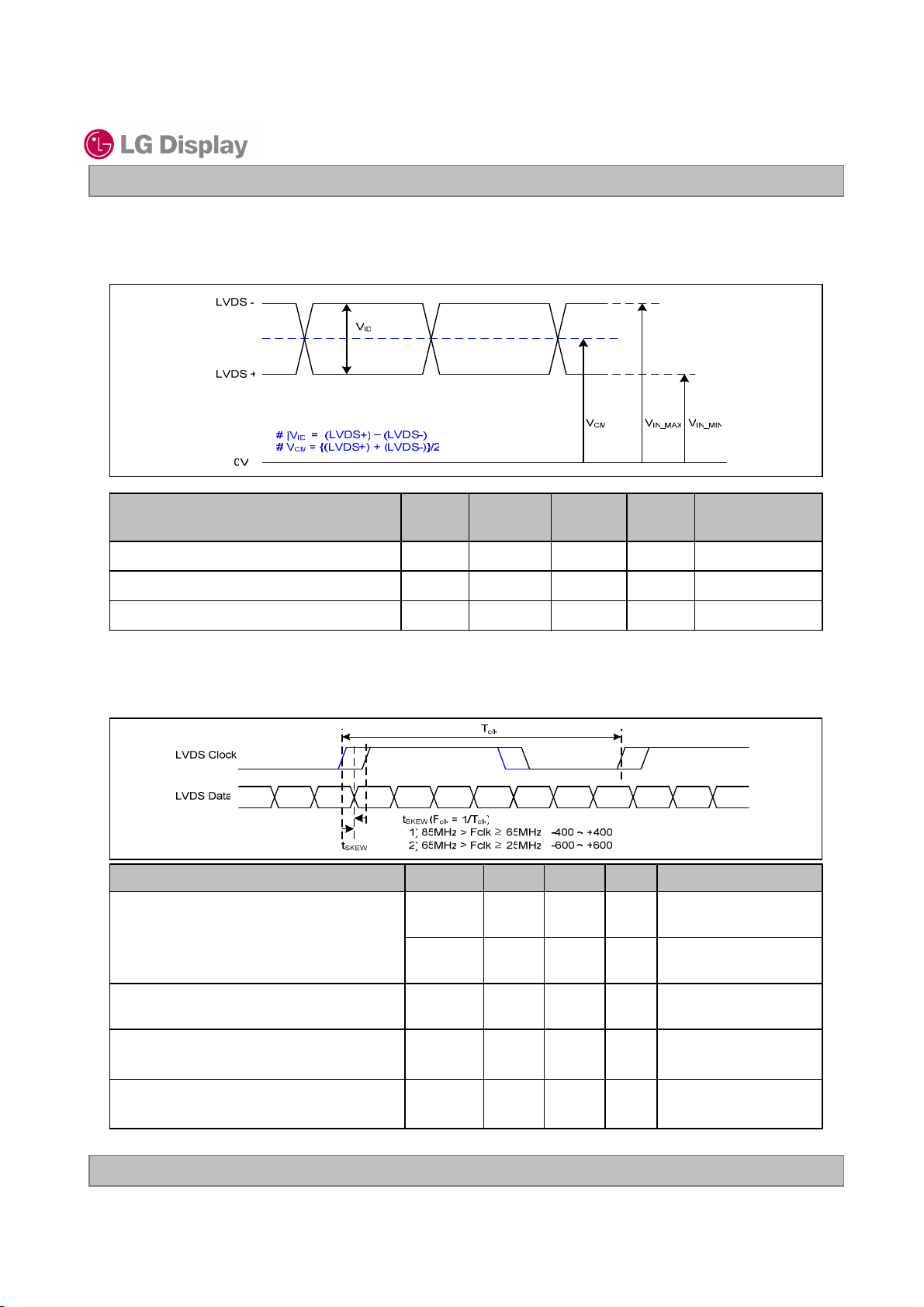
3-3. LVDS Signal Timing Specifications
3-3-1. DC Specification
LP141WX5
Liquid Crystal Display
Description
LVDS Common mode Voltage
LVDS Input Voltage Range
3-3-2. AC Specification
LVDS Clock to Data Skew Margin
Symb
ol
CM
IN
SKEW
SKEW
- 600
NotesUnitMaxMin
-mV600100|VID|LVDS Differential Voltage
-V1.80.6V
-V2.10.3V
NotesUnitMaxMinSymbolDescription
ps+ 400- 400t
ps+ 600t
85MHz > Fclk ≥
65MHz
65MHz > Fclk ≥
25MHz
LVDS Clock to Clock Skew Margin (Even
to Odd)
SKEW_EO
Maximum deviation
of input clock frequency during SSC
DEV
Maximum modulation frequency
of input clock during SSC
Ver. 1.0 Aug. 15, 2008
MOD
- 1/7
+ 1/7t
T
clk
%± 3-F
KHz200-F
-
-
-
9 / 32
Page 10
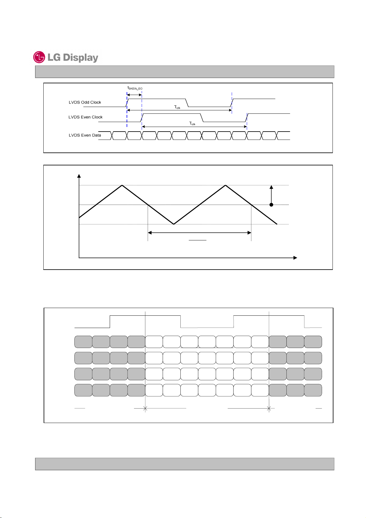
Freq.
F
max
F
center
F
min
Product Specification
< Clock skew margin between channel >
LP141WX5
Liquid Crystal Display
F
* F
center
DEV
3-3-3. Data Format
1) LVDS 1 Port
RCLK+
RA+/-
RB+/-
RC+/-
RD+/-
R3 R2
G4 G3
B5 B4
G7 G6
Previous (N-1)th Cycle Next (N+1)th Cycle
R1 R0
G2 G1
B3 B2
R7 R6
1
F
MOD
< Spread Spectrum >
G0 R5 R4 R3 R2 R1 R0
B1 B0 G5 G4 G3 G2 G1
DE VSYNC HSYNC B5 B4 B3 B2
X B7 B6 G7 G6 R7 R6
Current (Nth ) Cycle
Time
G0
B1
DE
VSYNC HSYNC
X
R5 R4
B0 G5
B7 B6
< LVDS Data Format >
Ver. 1.0 Aug. 15, 2008
10 / 32
Page 11

LP141WX5
Liquid Crystal Display
Product Specification
3-4. Signal Timing Specifications
This is the signal timing required at the input of the User connector. All of the interface signal timing should be
satisfied with the following specifications and specifications of LVDS Tx/Rx for its proper operation.
Table 5. TIMING TABLE
NoteUnitMaxTypMinSymbolITEM
FrequencyDCLK
Hsync
Width
Width-Active
Period
Vsync
Width
Width-Active
Horizontal back porch
Data
Enable
Horizontal front porch
Vertical back porch
Vertical front porch
3-5. Signal Timing Waveforms
Data Enable, Hsync, Vsync
DCLK
tCLK
0.5 Vcc
CLK
WH
WHA
VP
WV
WVA
HBP
HFP
VBP
VFP
High: 0.7VCC
Low: 0.3VCC
MHz-69.3-f
148014061360ThpPeriod
483216t
tCLK
128012801280t
860822809t
1062t
tHP
800800800t
964640t
tCLK
564824t
32136t
tHP
1831t
Condition : VCC =3.3V
t
Hsync
t
WH
t
HBP
HP
tWHA
Data Enable
t
VP
t
WV
Vsync
t
VBP
tWVA
Data Enable
Ver. 1.0 Aug. 15, 2008
t
t
HFP
VFP
11 / 32
Page 12

LP141WX5
Liquid Crystal Display
Product Specification
3-6. Color Input Data Reference
The brightness of each primary color (red,green and blue) is based on the 6-bit gray scale data input for the
color ; the higher the binary input, the brighter the color. The table below provides a reference for color
versus data input.
Table 6. COLOR DATA REFERENCE
Input Color Data
Basic
Color
RED
GREEN
BLUE
Color
Black
Red
Green
Blue
Cyan
Magenta
Yellow
White
RED (00)
RED (01)
…
RED (62)
RED (63)
GREEN (00)
GREEN (01)
...
GREEN (62)
GREEN (63)
BLUE (00)
BLUE (01)
…
BLUE (62)
BLUE (63)
RED
MSB LSB
GREEN
MSB LSB
BLUE
MSB LSB
B 5 B 4 B 3 B 2 B 1 B 0G 5 G 4 G 3 G 2 G 1 G 0R 5 R 4 R 3 R 2 R 1 R 0
0 0 0 0 0 00 0 0 0 0 00 0 0 0 0 0
0 0 0 0 0 00 0 0 0 0 01 1 1 1 1 1
0 0 0 0 0 01 1 1 1 1 10 0 0 0 0 0
1 1 1 1 1 10 0 0 0 0 00 0 0 0 0 0
1 1 1 1 1 11 1 1 1 1 10 0 0 0 0 0
1 1 1 1 1 10 0 0 0 0 01 1 1 1 1 1
0 0 0 0 0 01 1 1 1 1 11 1 1 1 1 1
1 1 1 1 1 11 1 1 1 1 11 1 1 1 1 1
0 0 0 0 0 00 0 0 0 0 00 0 0 0 0 0
0 0 0 0 0 00 0 0 0 0 00 0 0 0 0 1
………
0 0 0 0 0 00 0 0 0 0 01 1 1 1 1 0
0 0 0 0 0 00 0 0 0 0 01 1 1 1 1 1
0 0 0 0 0 00 0 0 0 0 00 0 0 0 0 0
0 0 0 0 0 00 0 0 0 0 10 0 0 0 0 0
………
0 0 0 0 0 01 1 1 1 1 00 0 0 0 0 0
0 0 0 0 0 01 1 1 1 1 10 0 0 0 0 0
0 0 0 0 0 00 0 0 0 0 00 0 0 0 0 0
0 0 0 0 0 10 0 0 0 0 00 0 0 0 0 0
………
1 1 1 1 1 00 0 0 0 0 00 0 0 0 0 0
1 1 1 1 1 10 0 0 0 0 00 0 0 0 0 0
Ver. 1.0 Aug. 15, 2008
12 / 32
Page 13

3-7. Power Sequence
LP141WX5
Liquid Crystal Display
Product Specification
Power Supply For LCD
VCC
Interface Signal,
V
i
(LVDS Signal of Transmitter)
LED Power
90%
0V
T
T
1
2
Valid Data
0V
T
3
Table 7. POWER SEQUENCE TABLE
90%
10%10%
T
T
6
5
T
4
T
7
OFFOFF LED ON
UnitsValueParameter
Max.Typ.Min.
1
2
3
4
5
6
7
(ms)10-0.5T
(ms)50-0T
(ms)--200T
(ms)--200T
(ms)50-0T
(ms)10-0T
(ms)--400T
Note)
1. Valid Data is Data to meet “3-3. LVDS Signal Timing Specifications”
2. Please avoid floating state of interface signal at invalid period.
3. When the interface signal is invalid, be sure to pull down the power supply for LCD VCC to 0V.
4. LED power must be turn on after power supply for LCD and interface signal are valid.
Ver. 1.0 Aug. 15, 2008
13 / 32
Page 14

LP141WX5
Liquid Crystal Display
Product Specification
4. Optical Specification
Optical characteristics are determined after the unit has been ‘ON’ and stable for approximately 30 minutes in
a dark environment at 25°C. The values specified are at an approximate distance 50cm from the LCD surface
at a viewing angle of Φ and Θ equal to 0°.
FIG. 1 presents additional information concerning the measurement equipment and method.
FIG. 1 Optical Characteristic Measurement Equipment and Method
Optical Stage(x,y)
Parameter Symbol NotesUnits
Surface Luminance, white
Luminance Variation
Response Time
Color Coordinates
RED
GREEN
BLUE
x axis, right(Φ=0°) degree--40Θr
x axis, left (Φ=180°)
y axis, up (Φ=90°)
y axis, down (Φ=270°)
LCD Module
50cm
Table 8. OPTICAL CHARACTERISTICS
Ta=25°C, VCC=3.3V, fV=60Hz, f
Values
MaxTypMin
WH
WHITE
TrR+ Tr
D
0.6040.5740.544RX
0.3790.3490.319RY
0.3650.3350.305GX
0.5720.5420.512GY
0.1860.1560.126BX
0.1660.1360.106BY
0.3430.3130.283WXWHITE
0.3590.3290.299WY
Pritchard 880 or
equivalent
CLK
-220200L
degree--40Θl
degree--10Θu
degree--30Θd
= 69.3MHz, I
2
= 20 mA
LED
1--500CRContrast Ratio
2cd/m
31.61.4-δ
4ms16
5Viewing Angle
6Gray Scale
Ver. 1.0 Aug. 15, 2008
14 / 32
Page 15

Liquid Crystal Display
Product Specification
Note)
1. Contrast Ratio(CR) is defined mathematically as
Surface Luminance with all white pixels
Contrast Ratio =
Surface Luminance with all black pixels
2. Surface luminance is the average of 5 point across the LCD surface 50cm from the surface with
all pixels displaying white. For more information see FIG 1.
LWH= Average(L1,L2, … L5)
LP141WX5
3. The variation in surface luminance , The panel total variation (δ
at each test position 1 through 13 and then defined as followed numerical formula.
For more information see FIG 2.
Maximum(L1,L2, … L13)
δ
4. Response time is the time required for the display to transition from white to black (rise time, TrR) and
from black to white(Decay Time, TrD). For additional information see FIG 3.
5. Viewing angle is the angle at which the contrast ratio is greater than 10. The angles are determined
for the horizontal or x axis and the vertical or y axis with respect to the z axis which is normal to the
LCD surface. For more information see FIG 4.
6. Gray scale specification * fV = 60Hz
WHITE
=
Minimum(L1,L2, … L13)
Luminance [%] (Typ)Gray Level
L0
L7
L15
L23
L31
L39
L47
L55
L63
) is determined by measuring L
WHITE
0.19
1.36
4.20
8.30
14.0
25.0
43.0
69.0
100
N
Ver. 1.0 Aug. 15, 2008
15 / 32
Page 16

Product Specification
FIG. 2 Luminance
<measuring point for surface luminance & measuring point for luminance variation>
H
LP141WX5
Liquid Crystal Display
A
C
L6
L7
D
L8
H,V : ACTIVE AREA
A : H/4 mm
B : V/4 mm
L2
L3
C : 10 mm
D : 10 mm
B
V
L9
L1
L10
POINTS : 13 POINTS
Center Point
L4 L5
L11 L13
FIG. 3 Response Time
The response time is defined as the following figure and shall be measured by switching the input signal
for “black” and “white”.
L12
Tr
R
%
100
90
Optical
Response
10
0
white
Ver. 1.0 Aug. 15, 2008
black
Tr
D
white
16 / 32
Page 17

FIG. 4 Viewing angle
LP141WX5
Liquid Crystal Display
Product Specification
<Dimension of viewing angle range>
φ
= 180
°
φ
= 270
,
Left
°
Down
Normal
Eye
Y
φ
= 90°, Up
θ
φ
°
Right
,
φ
= 0
,
Ver. 1.0 Aug. 15, 2008
17 / 32
Page 18

LP141WX5
Liquid Crystal Display
Product Specification
5. Mechanical Characteristics
The contents provide general mechanical characteristics for the model LP141WX5. In addition the figures
in the next page are detailed mechanical drawing of the LCD.
319.5 ± 0.5mmHorizontal
Outline Dimension
Bezel Area
Active Display Area
Surface Treatment
205.5 ± 0.5mmVertical
5.5mm (max)Thickness
306.76 ± 0.5mmHorizontal
193.00 ± 0.5mmVertical
303.74 mmHorizontal
189.84 mmVertical
360(Max)Weight
Glare treatment of the front polarizer
Ver. 1.0 Aug. 15, 2008
18 / 32
Page 19

Product Specification
LP141WX5
Liquid Crystal Display
<FRONT VIEW>
Note) Unit:[mm], General tolerance: ± 0.5mm
Ver. 1.0 Aug. 15, 2008
19 / 32
Page 20

Product Specification
LP141WX5
Liquid Crystal Display
<REAR VIEW>
Note) Unit:[mm], General tolerance: ± 0.5mm
FPC Pin Assignment
Pin
No.
DescriptionSymbol
LED PowerVin12
LED PowerVin11
LED PowerVin10
NCNC9
NCNC8
NCNC7
6th LED String FBFB66
5th LED String FBFB55
4th LED String FBFB44
3th LED String FBFB33
2nd LED String FBFB22
1st LED String FBFB11
Ver. 1.0 Aug. 15, 2008
20 / 32
Page 21

Product Specification
[ DETAIL DESCRIPTION OF SIDE MOUNTING SCREW ]
LP141WX5
Liquid Crystal Display
Notes : 1. Screw plated through the method of non-electrolytic nickel plating is preferred
to reduce possibility that results in vertical and/or horizontal line defect due to
the conductive particles from screw surface.
Ver. 1.0 Aug. 15, 2008
21 / 32
Page 22

Product Specification
LPL Proposal for system cover design.(Appendix)
LP141WX5
Liquid Crystal Display
1
Gap check for securing the enough gap between LCM
and System cover.
1.Rear side of LCM is sensitive against external stress,and previous check
about interference is highly needed.
Define
2.In case there is something from system cover comes into the boundary
above,mechanical interference may cause the FOS defects.
(Eg:Ripple,White spot..)
Check if antenna cable is sufficiently apart from T-CON of LCD Module.2
Define
NO GOOD
1.If system antenna is overlapped with T-CON,it might be cause the noise.
Ver. 1.0 Aug. 15, 2008
GOOD
22 / 32
Page 23

Product Specification
LPL Proposal for system cover design.
LP141WX5
Liquid Crystal Display
3
Define
Gap check for securing the enough gap between LCM
and System hinge.
1.At least 2.0mm of gap needs to be secured to prevent the shock
related defects.
2.”L” type of hinge is recommended than “I” type under shock test.
4
Checking the path of the System wire.
#4#5#6
Good
Ok
Bad
1.COF area needs to be handled with care.
2.GOOD Wire path design to system side.
Define
OK Wire path is located between COFs.
BADWire path overlapped with COF area.
Ver. 1.0 Aug. 15, 2008
#3
#2
#1
23 / 32
Page 24

Product Specification
LPL Proposal for system cover design.
5 Using a bracket on the top of LCM is not recommended.
bracket
LP141WX5
Liquid Crystal Display
Define
With bracket Without bracket
1.Condition without bracket is good for mechanical noise,and can minimize
the light leakage from deformation of bracket.
2.The results shows that there is no difference between the condition
with or without bracket.
Securing additional gap on CNT area..6
System cover inner side.
User connector
area.
User connector
Cable pathway.
A
A~A-1
A-1
cut
FPC:Flexible Printed Circuit.
1.CNT area is specially sensitive against external stress,and additional
Define
gap by cutting on system cover will be helpful on removing the Ripple.
2.Using a thinner CNT will be better. (eg: FPC type)
Ver. 1.0 Aug. 15, 2008
24 / 32
Page 25

6. Reliability
Environment test condition
LP141WX5
Liquid Crystal Display
Product Specification
ConditionsTest ItemNo.
Ta= 60°C, 240hHigh temperature storage test1
Ta= -20°C, 240hLow temperature storage test2
Ta= 50°C, 50%RH, 240hHigh temperature operation test3
Ta= 0°C, 240hLow temperature operation test4
Vibration test (non-operating)5
Shock test (non-operating)6
Altitude operating
7
storage / shipment
{ Result Evaluation Criteria }
There should be no change which might affect the practical display function when the display quality
test is conducted under normal operating condition.
Sine wave, 10 ~ 500 ~ 10Hz, 1.5G, 0.37oct/min
3 axis, 1hour/axis
Half sine wave, 180G, 2ms
one shock of each six faces(I.e. run 180G, 2ms
for all six faces)
0 ~ 10,000 feet (3,048m) 24Hr
0 ~ 40,000 feet (12,192m) 24Hr
Ver. 1.0 Aug. 15, 2008
25 / 32
Page 26

LP141WX5
Liquid Crystal Display
Product Specification
7. International Standards
7-1. Safety
a) UL 60950-1:2003, First Edition, Underwriters Laboratories, Inc.,
Standard for Safety of Information Technology Equipment.
b) CAN/CSA C22.2, No. 60950-1-03 1stEd. April 1, 2003, Canadian Standards Association,
Standard for Safety of Information Technology Equipment.
c) EN 60950-1:2001, First Edition,
European Committee for Electrotechnical Standardization(CENELEC)
European Standard for Safety of Information Technology Equipment.
7-2. EMC
a) ANSI C63.4 “Methods of Measurement of Radio-Noise Emissions from Low-Voltage Electrical and
Electrical Equipment in the Range of 9kHZ to 40GHz. “American National Standards Institute(ANSI),
1992
b) C.I.S.P.R “Limits and Methods of Measurement of Radio Interface Characteristics of Information
Technology Equipment.“ International Special Committee on Radio Interference.
c) EN 55022 “Limits and Methods of Measurement of Radio Interface Characteristics of Information
Technology Equipment.“ European Committee for Electrotechnical Standardization.(CENELEC), 1998
( Including A1: 2000 )
Ver. 1.0 Aug. 15, 2008
26 / 32
Page 27

Product Specification
8. Packing
8-1. Designation of Lot Mark
a) Lot Mark
A B C D E F G H I J K L M
A,B,C : SIZE(INCH) D : YEAR
E : MONTH F ~ M : SERIAL NO.
Note
1. YEAR
LP141WX5
Liquid Crystal Display
Year
Mark
2. MONTH
Month
Mark
b) Location of Lot Mark
Serial No. is printed on the label. The label is attached to the backside of the LCD module.
This is subject to change without prior notice.
8-2. Packing Form
a) Package quantity in one box : 30 pcs
b) Box Size : 484mm × 372mm × 288mm
2006720078200892009
6
Jun7Jul8Aug9Sep
6
321
200452005
4
Apr5May
4
200320022001
2010
0
Oct
A
Nov
B
DecMarFebJan
C321
Ver. 1.0 Aug. 15, 2008
27 / 32
Page 28

LP141WX5
Liquid Crystal Display
Product Specification
9. PRECAUTIONS
Please pay attention to the followings when you use this TFT LCD module.
9-1. MOUNTING PRECAUTIONS
(1) You must mount a module using holes arranged in four corners or four sides.
(2) You should consider the mounting structure so that uneven force (ex. Twisted stress) is not applied to the
module. And the case on which a module is mounted should have sufficient strength so that external
force is not transmitted directly to the module.
(3) Please attach the surface transparent protective plate to the surface in order to protect the polarizer.
Transparent protective plate should have sufficient strength in order to the resist external force.
(4) You should adopt radiation structure to satisfy the temperature specification.
(5) Acetic acid type and chlorine type materials for the cover case are not desirable because the former
generates corrosive gas of attacking the polarizer at high temperature and the latter causes circuit break
by electro-chemical reaction.
(6) Do not touch, push or rub the exposed polarizers with glass, tweezers or anything harder than HB
pencil lead. And please do not rub with dust clothes with chemical treatment.
Do not touch the surface of polarizer for bare hand or greasy cloth.(Some cosmetics are detrimental
to the polarizer.)
(7) When the surface becomes dusty, please wipe gently with absorbent cotton or other soft materials like
chamois soaks with petroleum benzene. Normal-hexane is recommended for cleaning the adhesives
used to attach front / rear polarizers. Do not use acetone, toluene and alcohol because they cause
chemical damage to the polarizer.
(8) Wipe off saliva or water drops as soon as possible. Their long time contact with polarizer causes
deformations and color fading.
(9) Do not open the case because inside circuits do not have sufficient strength.
9-2. OPERATING PRECAUTIONS
(1) The spike noise causes the mis-operation of circuits. It should be lower than following voltage :
V=± 200mV(Over and under shoot voltage)
(2) Response time depends on the temperature.(In lower temperature, it becomes longer.)
(3) Brightness depends on the temperature. (In lower temperature, it becomes lower.)
And in lower temperature, response time(required time that brightness is stable after turned on) becomes
longer.
(4) Be careful for condensation at sudden temperature change. Condensation makes damage to polarizer or
electrical contacted parts. And after fading condensation, smear or spot will occur.
(5) When fixed patterns are displayed for a long time, remnant image is likely to occur.
(6) Module has high frequency circuits. Sufficient suppression to the electromagnetic interference shall be
done by system manufacturers. Grounding and shielding methods may be important to minimized the
interference.
Ver. 1.0 Aug. 15, 2008
28 / 32
Page 29

LP141WX5
Liquid Crystal Display
Product Specification
9-3. ELECTROSTATIC DISCHARGE CONTROL
Since a module is composed of electronic circuits, it is not strong to electrostatic discharge. Make certain that
treatment persons are connected to ground through wrist band etc. And don’t touch interface pin directly.
9-4. PRECAUTIONS FOR STRONG LIGHT EXPOSURE
Strong light exposure causes degradation of polarizer and color filter.
9-5. STORAGE
When storing modules as spares for a long time, the following precautions are necessary.
(1) Store them in a dark place. Do not expose the module to sunlight or fluorescent light. Keep the
temperature between 5°C and 35°C at normal humidity.
(2) The polarizer surface should not come in contact with any other object.
It is recommended that they be stored in the container in which they were shipped.
9-6. HANDLING PRECAUTIONS FOR PROTECTION FILM
(1) When the protection film is peeled off, static electricity is generated between the film and polarizer.
This should be peeled off slowly and carefully by people who are electrically grounded and with well
ion-blown equipment or in such a condition, etc.
(2) The protection film is attached to the polarizer with a small amount of glue. If some stress is applied
to rub the protection film against the polarizer during the time you peel off the film, the glue is apt to
remain on the polarizer.
Please carefully peel off the protection film without rubbing it against the polarizer.
(3) When the module with protection film attached is stored for a long time, sometimes there remains a
very small amount of glue still on the polarizer after the protection film is peeled off.
(4) You can remove the glue easily. When the glue remains on the polarizer surface or its vestige is
recognized, please wipe them off with absorbent cotton waste or other soft material like chamois
soaked with normal-hexane.
Ver. 1.0 Aug. 15, 2008
29 / 32
Page 30

LP141WX5
F ea tur e Sup po rt ( no_ DP MS, no _ A ct ive O ff/ V ery L ow P ow er , R GB co lo r d isp la y, T im in g B LK
Establ
Liquid Crystal Display
Product Specification
APPENDIX A. Enhanced Extended Display Identification Data (EEDIDTM) 1/3
E DID D a ta fo r L E N O V O _
ver . 1.0
20 08 . 8. 15 .
B yte
(D ec )
Version
Vendor / Product EDID
Display
Parameters
Panel Color Coordinates
ished
Timin
Standard Timing ID Header
B yte
(H ex )
0
1
2
3
4
5
6
7
8
9
10
11
12
13
14
15
16
17
18
19
20
21
22
23
24
25
26
27
28
29
30
31
32
33
34
35
36
37
38
39
40
41
42
43
44
45
46
47
48
49
50
51
52
53
H ead er
0 0
H ead er
0 1
H ead er
0 2
H ead er
0 3
H ead er
0 4
H ead er
0 5
H ead er
0 6
H ead er
0 7
E IS A m an ufa ctu re co de ( 3 C har act er ID ) L GD
0 8
E IS A m an ufa ctu re co de (C om pre sse d A SCⅡ)
0 9
P an el S up pli er R es er ved - P rod uc t C o de 01 91h
0A
( H e x. LS B f ir st )
0B
L CD M odu le Ser ial N o - P ref er red bu t O p ti o na l (" 0" I f not use d)
0C
L CD M odu le Ser ial N o - P ref er red bu t O p ti o na l (" 0" I f not use d)
0D
L CD M odu le Ser ial N o - P ref er red bu t O p ti o na l (" 0" I f not use d)
0E
L CD M odu le Ser ial N o - P ref er red bu t O p ti o na l (" 0" I f not use d)
0F
W eek o f M anu fac tur e 0 we eks
1 0
Y ear o f M anuf act ur e 2 00 8ye ars
1 1
E D ID stru ctu re v ers ion # = 1
1 2
E D ID rev isio n # = 3
1 3
V ide o i np ut D efin itio n = Dig it al sig nal
1 4
M ax H i m age s ize ( R oun ded cm ) = 3 0 c m
1 5
M ax V i m age s ize ( R oun ded cm ) = 1 9 c m
1 6
D ispla y ga mm a = (gam ma *10 0)-1 00 = Ex am ple :( 2 .2 *10 0)- 10 0= 12 0 = 2.2 G am m a
1 7
1 8
R ed /G ree n L ow Bit s (Rx Ry/ Gx G y)
1 9
B lu e/W hi te Lo w B its ( B x B y/W xW y)
1A
R ed X R x = 0. 57 4
1B
R ed Y R y = 0 .34 9
1C
G ree n X G x = 0 .33 5
1D
G ree n Y G y =0. 5 42
1E
B lu e X Bx = 0 .15 6
1F
B lu e Y By = 0 .13 6
2 0
W hit e X W x = 0.3 13
2 1
W hit e Y W y = 0.3 29
2 2
E st a bl ishe d t imi ng 1 (0 0h if no t u se d)
2 3
E st a bl ishe d t imi ng 2 (0 0h if no t u se d)
2 4
M anu fac ture r's tim in gs (0 0h if n o t us ed)
2 5
S ta n da rd tim in g ID 1 (01 h if no t use d)
2 6
S ta n da rd tim in g ID 1 (01 h if no t use d)
2 7
S ta n da rd tim in g ID 2 (01 h if no t use d)
2 8
S ta n da rd tim in g ID 2 (01 h if no t use d)
2 9
S ta n da rd tim in g ID 3 (01 h if no t use d)
2A
S ta n da rd tim in g ID 3 (01 h if no t use d)
2B
S ta n da rd tim in g ID 4 (01 h if no t use d)
2C
S ta n da rd tim in g ID 4 (01 h if no t use d)
2D
S ta n da rd tim in g ID 5 (01 h if no t use d)
2E
S ta n da rd tim in g ID 5 (01 h if no t use d)
2F
S ta n da rd tim in g ID 6 (01 h if no t use d)
3 0
S ta n da rd tim in g ID 6 (01 h if no t use d)
3 1
S ta n da rd tim in g ID 7 (01 h if no t use d)
3 2
S ta n da rd tim in g ID 7 (01 h if no t use d)
3 3
S ta n da rd tim in g ID 8 (01 h if no t use d)
3 4
S ta n da rd tim in g ID 8 (01 h if no t use d)
3 5
Field N a m e an d C om m e n ts
V alu e
(H ex )
00
FF
FF
FF
FF
FF
FF
00
30
E 4
91
01
00
00
00
00
00
12
01
03
80
1E
13
78
0A
1F
35
93
59
55
8A
28
22
50
54
00
00
00
01
01
01
01
01
01
01
01
01
01
01
01
01
01
01
01
V alu e
(B in)
00 00 000 0
11 11 111 1
11 11 111 1
11 11 111 1
11 11 111 1
11 11 111 1
11 11 111 1
00 00 000 0
00 11 000 0
11 10 010 0
10 01 000 1
00 00 000 1
00 00 000 0
00 00 000 0
00 00 000 0
00 00 000 0
00 00 000 0
00 01 001 0
00 00 000 1
00 00 001 1
10 00 000 0
00 01 111 0
00 01 001 1
01 11 100 0
00 00 101 0
00 01 111 1
00 11 010 1
10 01 001 1
01 01 100 1
01 01 010 1
10 00 101 0
00 10 100 0
00 10 001 0
01 01 000 0
01 01 010 0
00 00 000 0
00 00 000 0
00 00 000 0
00 00 000 1
00 00 000 1
00 00 000 1
00 00 000 1
00 00 000 1
00 00 000 1
00 00 000 1
00 00 000 1
00 00 000 1
00 00 000 1
00 00 000 1
00 00 000 1
00 00 000 1
00 00 000 1
00 00 000 1
00 00 000 1
Ver. 1.0 Aug. 15, 2008
30 / 32
Page 31

LP141WX5
Pi xe l C lock /10,00 0 (L SB ) 6 9. 3 M Hz @ 59.9 6H z
co de 0 A h,se t r em ainin g char = 2 0h)
co de 0 A h,se t r em ainin g char = 2 0h)
co de 0 A h,se t r em ainin g char = 2 0h)
Liquid Crystal Display
Product Specification
APPENDIX A. Enhanced Extended Display Identification Data (EEDIDTM) 2/3
By te
(D ec)
Timing Descriptor #1Timing Descriptor #2Timing Descriptor #3
54
55
56
57
58
59
60
61
62
63
64
65
66
67
68
69
70
71
72
73
74
75
76
77
78
79
80
81
82
83
84
85
86
87
88
89
90
91
92
93
94
95
96
97
98
99
10 0
10 1
10 2
10 3
10 4
10 5
10 6
10 7
By te
(H ex)
36
Pi xe l C lock /10,00 0 (M SB)
37
Ho rizo nt al A ct ive (lo wer 8 bi ts) 12 80 Pi xe ls
38
Ho rizo nt al B la nk in g( Thp -H A) (low er 8 b its) 1 26 P ixels
39
Ho rizo nt al A ct ive / Hor izon ta l B lank in g( T hp -HA) (up pe r 4: 4b its)
3A
Ve rt ic al A vtive 8 0 0 Li ne s
3B
Ve rt ic al B la nk in g (T vp-HA ) (D E B lanking t yp .for DE on ly pan el s) 2 2 Line s
3C
Ve rt ic al A ctive : V erti ca l B lank ing ( T vp -HA ) ( up per 4: 4b its)
3D
Ho rizo nt al Sync. O ffs et (T hfp) 48 Pix els
3E
Ho rizo nt al Sync P ulse W idth (HSP W) 32 Pixels
3F
Ve rt ic al S ync O ffse t(Tv fp ) : Sy nc Wid th (VS PW ) 3 Li ne s : 6 Line s
40
Ho rizo nt al V er tic al S yn c O ffs et /W idth (u ppe r 2 bits )
41
Ho rizo nt al Im age Si ze ( mm ) 3 04 m m
42
Ve rt ic al Im age Si ze (m m) 1 90 mm
43
Ho rizo nt al Im age Si ze / V er tica l I ma ge S iz e
44
Ho rizo nt al B or der = 0 (Z er o fo r Note boo k LC D)
45
Ve rt ic al B or d er = 0 (Zero fo r N otebo ok L CD )
46
No n-Interla ce , No rm al disp lay, no s te re o, D ig ita l Sep arat e ( V sync _NE G, H sync _NE G )
47
Fla g
48
Fla g
49
Fla g
4A
Da ta T ype Tag (D es cr ip tor D efin ed b y ma nufactu rer )
4B
Fla g
4C
De sc ripto r De fine d by m anu factu rer
4D
De sc ripto r De fine d by m anu factu rer
4E
De sc ripto r De fine d by m anu factu rer
4F
De sc ripto r De fine d by m anu factu rer
50
De sc ripto r De fine d by m anu factu rer
51
De sc ripto r De fine d by m anu factu rer
52
De sc ripto r De fine d by m anu factu rer
53
De sc ripto r De fine d by m anu factu rer
54
De sc ripto r De fine d by m anu factu rer
55
De sc ripto r De fine d by m anu factu rer
56
De sc ripto r De fine d by m anu factu rer
57
De sc ripto r De fine d by m anu factu rer
58
De sc ripto r De fine d by m anu factu rer
59
Fla g
5A
Fla g
5B
Fla g
5C
Da ta T ype Tag ( A SC II S tring )
5D
Fla g
5E
AS C II S tri ng L
5F
AS C II S tri ng G
60
AS C II S tri ng
61
AS C II S tri ng D
62
AS C II S tri ng i
63
AS C II S tri ng s
64
AS C II S tri ng p
65
AS C II S tri ng l
66
AS C II S tri ng a
67
AS C II S tri ng y
68
M an uf ac tu re r P/ N(If <1 3 ch ar -- > 0A h, th en t ermi na te w ith A SC
69
M an uf ac tu re r P/ N(If <1 3 ch ar -- > 0A h, th en t ermi na te w ith A SC
6A
M an uf ac tu re r P/ N(If <1 3 ch ar -- > 0A h, th en t ermi na te w ith A SC
6B
Field N ame and C omm ents
Ⅱ
Ⅱ
Ⅱ
Va lue
(H ex)
12
1B
00
7E
50
20
16
30
30
20
36
00
30
BE
10
00
00
18
00
00
00
00
00
00
00
00
00
00
00
00
00
00
00
00
00
00
00
00
00
FE
00
4C
47
20
44
69
73
70
6C
61
79
0A
20
20
Va lue
(B in)
00 01 001 0
00 01 101 1
00 00 000 0
01 11 111 0
01 01 000 0
00 10 000 0
00 01 011 0
00 11 000 0
00 11 000 0
00 10 000 0
00 11 011 0
00 00 000 0
00 11 000 0
10 11 111 0
00 01 000 0
00 00 000 0
00 00 000 0
00 01 100 0
00 00 000 0
00 00 000 0
00 00 000 0
00 00 000 0
00 00 000 0
00 00 000 0
00 00 000 0
00 00 000 0
00 00 000 0
00 00 000 0
00 00 000 0
00 00 000 0
00 00 000 0
00 00 000 0
00 00 000 0
00 00 000 0
00 00 000 0
00 00 000 0
00 00 000 0
00 00 000 0
00 00 000 0
11 11 111 0
00 00 000 0
01 00 110 0
01 00 011 1
00 10 000 0
01 00 010 0
01 10 100 1
01 11 001 1
01 11 000 0
01 10 110 0
01 10 000 1
01 11 100 1
00 00 101 0
00 10 000 0
00 10 000 0
Ver. 1.0 Aug. 15, 2008
31 / 32
Page 32

LP141WX5
Checksum
Liquid Crystal Display
Product Specification
APPENDIX A. Enhanced Extended Display Identification Data (EEDIDTM) 3/3
Byte
(Dec)
Timing Descriptor #4
108
109
110
111
112
113
114
115
116
117
118
119
120
121
122
123
124
125
126
127
Byte
(Hex)
Flag
6C
Flag
6D
Flag
6E
Data Type Tag ( Monitor Name, stored as ASCII )
6F
Flag
70
Monitor Name, stored as ASCII L
71
Monitor Name, stored as ASCII P
72
Monitor Name, stored as ASCII 1
73
Monitor Name, stored as ASCII 4
74
Monitor Name, stored as ASCII 1
75
Monitor Name, stored as ASCII W
76
Monitor Name, stored as ASCII X
77
Monitor Name, stored as ASCII 5
78
Monitor Name, stored as ASCII -
79
Monitor Name, stored as ASCII T
7A
Monitor Name, stored as ASCII L
7B
Monitor Name, stored as ASCII D
7C
Monitor Name, stored as ASCII 1
7D
Extension flag (# of optional 128 panel ID extension block to follow, Typ = 0)
7E
Check Sum (The 1-byte sum of all 128 bytes in this panel ID block shall = 0)
7F
Field Name and Comments
Value
(Hex)
00
00
00
FC
00
4C
50
31
34
31
57
58
35
2D
54
4C
44
31
00
D8
Value
(Bin)
00000000
00000000
00000000
11111100
00000000
01001100
01010000
00110001
00110100
00110001
01010111
01011000
00110101
00101101
01010100
01001100
01000100
00110001
00000000
11011000
Ver. 1.0 Aug. 15, 2008
32 / 32
 Loading...