

Page 1
Global LCD Panel Exchange Center
www.panelook.com
LP141WX3
Liquid Crystal Display
Product Specification
SPECIFICATION
FOR
APPROVAL
()Preliminary Specification
( ଝ ) Final Specification
Title 14.1” WXGA TFT LCD
Customer HP
MODEL
APPROVED BY SIGNATURE
/
/
SUPPLIER LG Display Co., Ltd.
*MODEL LP141WX3
Suffix TLN4
*When you ob tain standard approval,
please use the ab ove model name without suff ix
APPROVED BY
G.J. Kwon / G.Manag er
REVIEWED BY
S. R. Kim / Manager
SIGNATURE
/
Pleas e return 1 cop y for your conf irmation with
yo ur signature and comments.
Ver. 1.0 Nov. 25, 2009
PREPARED BY
S.Y. Kim / Engineer
M.S. Ahn / Eng ineer
Products Engineering Dept.
LG Display Co., Ltd
One step solution for LCD / PDP / OLED panel application: Datasheet, inventory and accessory!
1/ 31
www.panelook.com
Page 2
Global LCD Panel Exchange Center
www.panelook.com
LP141WX3
Liquid Crystal Display
Product Specification
Contents
No ITEM
COVER
CONTENTS
REC ORD OF REV ISIONS
1 GENERAL DESCRIPTION
2 ABSOLUTE MAXIMUM RATINGS
3 ELECTRICAL SPECIFICATIONS
3-1 ELECTRICAL CHARACTREISTICS
3-2 INTERFACE CONNECTIONS
3-3 LVDS SIGNAL TIMING SPECIFICATIONS
3-4 SIGNAL TIMING SPECIFICATIONS
3-5 SIGN AL TIMING WAVEFORMS
3-6 COLOR INPUT DATA REFERNECE
3-7 POWER SEQUENCE
4 OPTICAL SFECIFICATIONS
Page
1
2
3
4
5
6
8
9
11
11
12
13
14
5 MECHANICAL CHARACTERISTICS
6 RELIABLITY
7 INTERNATIONAL STANDARDS
7-1 SAFETY
7-2 EMC
8 PACKING
8-1 DESIGNATION OF LOT MARK
8-2 PACKING FORM
9 PRECAUTIONS
A APPENDIX. Enhanced Extended Display Identification Data
Ver. 1.0 Nov. 25, 2009
17
24
25
25
26
26
27
29
2/ 31
One step solution for LCD / PDP / OLED panel application: Datasheet, inventory and accessory!
www.panelook.com
Page 3
Global LCD Panel Exchange Center
www.panelook.com
LP141WX3
Liquid Crystal Display
Product Specification
RECORD OF REVISIONS
Revision No Revision Date Page Description
0.0 Sep. 24. 2009 - First Draft (Preliminary Specification) 0.0
1.0 Nov. 25. 2009 - Final Specification 1.0
19 Update the Drawing
26 Update the Packing Information
29~31 Update the EDID DATA
EDID
ver
Ver. 1.0 Nov. 25, 2009
One step solution for LCD / PDP / OLED panel application: Datasheet, inventory and accessory!
3/ 31
www.panelook.com
Page 4
Global LCD Panel Exchange Center
1. General Description
The LP141 WX3 is a Color Active Matrix Liquid Crystal Disp lay with an integ ral Cold Cathode Fluorescent
Lamp (CCFL) backlight system. The matrix emp loys a-Si Thin Film Transis to r as the active element. It is a
transmissive type disp lay operating in the normally white mod e. This TFT-L CD has 14.1 inches diagonally
measured active d isplay area with WXGA resolution(800 vertical by 1280 horizontal p ixel arr ay). Each p ixel
is divided into Red, Green and Blue sub -pixels or dots which are arranged in vertical stripes. Gray scale or
the brightness of the sub-p ixel c olor is determined with a 6-b it gray scale signal for each dot, thus,
presenting a palette of more than 262,144 c olors.
The LP141WX3 has been designed to apply the interf ace method that enables low power, hig h speed, lo w
EMI.
The LP141WX3 is intended to support applications where thin thic kness, low po wer are critical f actors and
graphic display s are important. In combination with the vertical arrangement of the sub -pixels, the
LP141 WX3 characteristics p rovide an excellent flat disp lay for office automatio n products such as Notebook
PC.
www.panelook.com
LP141WX3
Liquid Crystal Display
Product Specification
ڞک
ڌ
ڰێۀۍٻھۊۉۉۀھۏۊۍٻ
ڎڋ
ګۄۉ
ڧڱڟڮٻځ
گۄۈۄۉۂ
ڞۊۉۏۍۊۇ
ڝۇۊھۆ
ګڪڲڠڭٻ
ڝڧڪڞڦ
ڠڟڤڟٻ
ڮۊېۍھۀٻڟۍۄۑۀۍٻڞۄۍھېۄۏ
ڌ
ڌ
ڢڤګڃڢڼۏۀٻڤۉٻګڼۉۀۇڄ
ړڋڋ
ڌڍړڋ
گڡگڈڧڞڟٻګڼۉۀۇ
ڃڌڍړڋٻۓٻړڋڋڄ
ڝڧڪڞڦ
ڞک
ڝڼھۆۇۄۂۃۏٻڜێێ’۔
ࣿࣜࣜ ࣜࣜࣜ
General Features
Active Screen Size 14.1 in ches diagonal
Outline Dimension
Pixel Pitch 0.2373mm Ý 0.2373 mm
Pixel Format 1280 horiz. By 800 vert. Pixels RGB strip arrangement
Color Depth 6-bit, 262,144 colors
Luminance, White 200 cd/m
Power Consumption Total 5.2 Watt(Typ.) @ LCM circuit 1.2 Watt (Typ._Mosaic), B/L input 4.0Watt(Typ.)
Weight 400g(Max.)
Display Operating Mode Transmissive mode, normally white
Surface Treatment Glare treatment of the front polarizer
RoHS Comply Yes
319.5(H,Typ.) ϧ 205.5(V,Typ.) ϧ 5.5(D,Max) [mm]
2
(Typ.5 point)
Ver. 1.0 Nov. 25, 2009
One step solution for LCD / PDP / OLED panel application: Datasheet, inventory and accessory!
4/ 31
www.panelook.com
Page 5
Global LCD Panel Exchange Center
2. Absolute Maximum Ratings
The f ollo wing are maximum v alues whic h, if exceed ed, may cause f aulty operatio n or damage to the unit.
www.panelook.com
LP141WX3
Liquid Crystal Display
Product Specification
Table 1. ABSOLUTE MAXIMUM RATINGS
Param eter Sym bol
Power Input Voltage
Operating Temperature
Storag e Temperature
Operating Ambient Humid ity
Storag e Humid ity
VCC -0.3 4.0 Vdc at 25 r 5qC
TOP 050qC1
HST -20 60 qC1
HOP 10 90 %RH 1
HST 10 90 %RH 1
Values
Units Notes
Min Max
Note : 1. Temperature and relative humidity rang e are shown in the f igure below.
Wet bulb temperature should be 39
Wet Bulb
Temperature [к]
30
20
10
0
qC Max, and no condensation o f water.
90% 80%
60
50
40
60%
Humidity[(%)RH]
40%
20%
10%
Storage
Operation
-20
10
20 30 40 50
60 70 800
Dry Bulb Temperature [к]
Ver. 1.0 Nov. 25, 2009
One step solution for LCD / PDP / OLED panel application: Datasheet, inventory and accessory!
5/ 31
www.panelook.com
Page 6
Global LCD Panel Exchange Center
3. Electrical Specifications
3-1. Electrical Characteristics
The LP141WX 3 req uires two power inputs. One is emp lo yed to power the LCD electronic s and to d rive the
TFT array and liquid crystal. The second input which powers the CCF L, is typically generated by an
inverter. The inverter is an external unit to the LCD.
Param eter Symbol
MODULE :
Power Supply Input Voltage VCC 3.0 3.3 3.6 V
Power Supply Input Current I
Power Consumption Pc Mosaic - 1.2 1.4
Differential Impedance Zm 90 100 110 Ohm 2
LAMP :
Operating Voltage V
Operating Current I
Power Consumption P
Operating Frequency f
Discharge Stabilization Time Ts 3 Min 4
Life Time 15,000 Hrs 5
www.panelook.com
Product Specification
Table 2. ELECTRICAL CHARACTERISTICS
Values
Min Typ Max
CC
Mosaic - 360 414 mA 1
BL
BL
BL
BL
640(7.0mA) 670(6.0mA) 880(2.0mA) V
2.0 6.0 7.0 mA
1.8 4.0 4.5 W
45 55 80 kHz
LP141WX3
Liquid Crystal Display
Unit Notes
DC
RMS
RMS
3
Established Starting Voltage
at 25к
at 0 к
Vs
1180
1415
V
RMS
V
RMS
Note)
1. The sp ecified current and power consump tion are under the Vcc = 3.3V , 25к, fv = 60Hz condition
whereas Mos aic pattern is d isplayed and fv is the f rame f requency.
2. This impedance value is needed to proper display and measured f orm LVD S Tx to the mating connector.
3. The typical o perating current is for the typical surf ace luminance (LWH) in optical characteristics.
4. Define the brightness of the lamp af ter being lighted f or 5 minutes as 100%, Ts is the time req uired f o r
the brightness of the center of the lamp to be not less than 95%.
5. The lif e time is determined as the time at which brig htnes s o f lamp is 50% compare to that of initial value
at the typ ical lamp current.
Ver. 1.0 Nov. 25, 2009
6/ 31
One step solution for LCD / PDP / OLED panel application: Datasheet, inventory and accessory!
www.panelook.com
Page 7
Global LCD Panel Exchange Center
Note)
6. The o utp ut of the inverter must have symmetrical(negative and positive) vo ltage wavef orm and
symmetrical current waveform.(Asymmetrical ratio is less than 10%) Please d o not use the inverter
which has asy mmetrical voltage and asymmetrical current and spike wave.
Lamp frequency may produce interf ace with horizo ntal synchro nous f requency and as a result this may
cause beat on the d isplay. Theref ore lamp f requency shall be as away possible from the
horizontal sync hronous frequency and from its harmonics in ord er to prevent interference.
7. It is def ined the brig htnes s o f the lamp after being lighted f or 5 minutes as 100%.
is the time required f or the brightness of the center of the lamp to be not less than 95%.
T
S
8. The lamp po wer co nsumption shown abo ve does no t includ e loss of external inverter.
The app lied lamp current is a typical o ne.
9. Requirements for a system inverter design, which is intended to have a better display performance, a
better p ower ef f iciency and a more reliable lamp, are f o llo wing.
It shall help increase the lamp lifetime and reduce leakage current.
a. The asymmetry rate of the inverter waveform should be less than 10%.
b. The distortion rate of the waveform should be within √2 ·10%.
* Inverter output waveform had better be more similar to ideal sine wave.
www.panelook.com
LP141WX3
Liquid Crystal Display
Product Specification
* Asymmetry rate:
I p
|I
p
– I–p|/I
rms
* 100%
* Distortion rate
I -p
(or I–p)/I
I
p
rms
10. Inverter op en voltage must be more than lamp vo ltage f or more than 1 second f or start -up.
Otherwis e, the lamps may not be turned on.
ϡ Do no t attach a conducting tape to lamp connecting wire.
If the lamp wire attach to a conducting tape, TFT-LCD Module has a low luminance and the inverter
has abnormal ac tion. Because leakage current is occurred between lamp wire and co nducting tape.
Ex of current wave)
Normal current wave - Standard
Abnormal current wave - Bad
Abnormal current wave - Bad
Ver. 1.0 Nov. 25, 2009
Abnormal current wave - Bad
One step solution for LCD / PDP / OLED panel application: Datasheet, inventory and accessory!
7/ 31
www.panelook.com
Page 8
Global LCD Panel Exchange Center
3-2. Interface Connections
This LCD employs two interf ace co nnections, a 30 p in co nnector is used f or the mod ule electronics interf ace
and the other connector is used for the integral backlig ht system.
The electronics interf ace c onnecto r is a mod el MDF76LBRW-30S-1 manuf actured b y HIROSE.
Table 3. MODULE CONNECTOR PIN CONFIGURATION (CN1)
Pin Symbol Description Notes
1 GND Ground
2 VCC Power Supply, 3.3V Typ.
3 VCC Power Supply, 3.3V Typ.
4 V EEDID DDC 3.3V power
5
6 Clk EEDID DDC Clo ck
7 DATA EEDID DDC Data
8R
9R
10 GND Gr oun d
11 R
12 RIN1+ Pos itive LVDS d ifferenti al data input
13 GND Gr oun d
14 R
15 R
16 GND Gr oun d
17 CLKIN- Neg ative LVDS d ifferential clock input
18 CLKIN+ Pos itive LVDS differenti al clock in put
19 GND Groun d
20 NC No Con nect
21 NC No Con nect
22 GND Gr oun d
23 NC No Con nect
24 NC No Con nect
25 GND Gr oun d
26 NC No Con nect
27 NC No Con nect
28 GND Gr oun d
29 NC No Con nect
30 NC No Con nect
The backlight interf ace connecto r is a mod el BHSR-02VS-1, manufactured by JST or Comp atible.
The mating connec to r part number is AMP1674817-2 or equivalent.
NC Reserved for supplier test point
0- Neg ative LVDS differential data input
IN
0+ Pos itive LVDS d ifferenti al data input
IN
1- Neg ative LVDS differential data input
IN
2- Neg ative LVDS differential data input
IN
2+ Pos itive LVDS d ifferenti al data input
IN
Table 4. BACKLI GHT CONNECTOR PIN CONFIGURATION (J3)
www.panelook.com
Product Specification
LP141WX3
Liquid Crystal Display
1, In terface chips
1.1 LCD : SW, SW0612B (LCD Controller)
in cluding LVDS Recei ver
1.2 System : THC63LVD823A o r equi valent
* Pin to Pin co mpatible with LVDS
2. Connector
2.1 LCD : MDF76LBRW-30S-1,HIROSE
2.2 Matin g : FI-X30M or equivalent.
2.3 Connector pin arrangement
ZW
FI-XB30SRL-HF 11, JAE
its compatibles
X
[LCD Mo dule Rear View]
PIN1
PIN2PIN2
Pin Symbol Description Notes
1 HV Power sup ply for lamp (High voltage side) 1
2 LV Po wer sup ply for lamp (Low v oltage side) 1
Notes : 1. The high voltage sid e terminal is colored White and the low voltage sid e terminal is Yellow.
Ver. 1.0 Nov. 25, 2009
One step solution for LCD / PDP / OLED panel application: Datasheet, inventory and accessory!
8/ 31
www.panelook.com
Page 9
Global LCD Panel Exchange Center
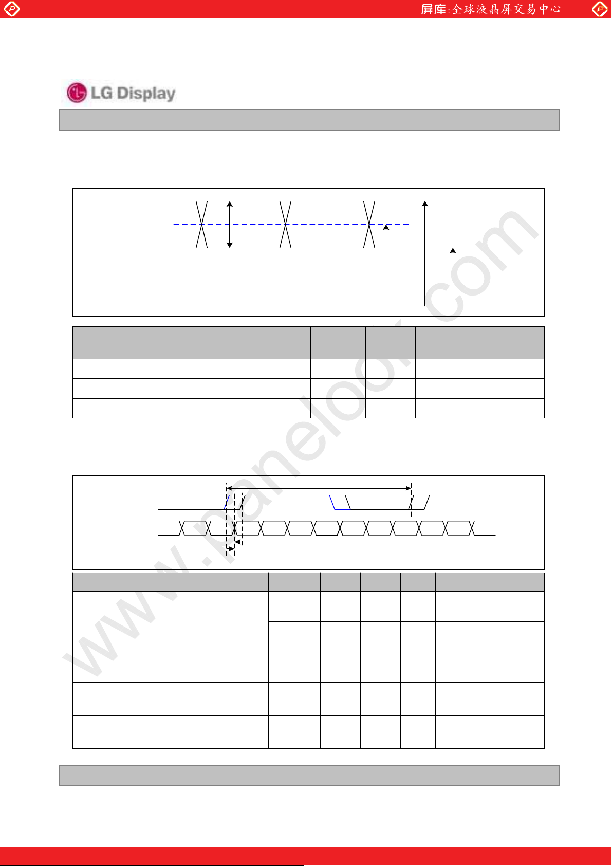
3-3. LVDS Signal Timing Specifications
3-3-1. DC Specification
LVDS -
LVDS +
www.panelook.com
LP141WX3
Liquid Crystal Display
Product Specification
|VID|
#|VID| = |(LVDS+) ˀ (LVDS-)|
= {(LVDS+) + (LVDS-)}/2
#V
0V
CM
Description
LVDS Dif f erential Vo ltage |V
LVDS Commo n mode Voltage V
LVDS Input Vo ltage Range V
3-3-2. AC Specification
LVDS Clock
LVDS Data
t
SKEW
V
CM
Symb
ol
| 100 600 mV -
ID
CM
IN
t
=1/T
SKEW(Fclk
1) 85MHz > Fclk ˻ 65MHz : -400 ~ +400
2) 65MHz > Fclk ˻ 25MHz : -600 ~ +600
Min Max Unit Notes
0.6 1.8 V -
0.3 2.1 V -
T
clk
)
clk
V
IN_MAXVIN_MIN
Description Symbol Min Max Unit Notes
t
SKEW
- 400 + 400 p s
85MHz > Fclk ≥
65MHz
LVDS Clock to Data Skew Margin
t
SKEW
LVDS Clo ck to Clo ck Skew Margin (Even
to Odd)
Maximum deviation
of input clock frequency during SSC
Maximum modulation f requency
of input clock during SSC
t
SKEW_EO
F
DEV
F
MOD
Ver. 1.0 Nov. 25, 2009
- 600 + 600 p s
-1/7 + 1/7 T
clk
- · 3% -
- 200 KHz -
65MHz > Fclk ≥
25MHz
One step solution for LCD / PDP / OLED panel application: Datasheet, inventory and accessory!
-
9/ 31
www.panelook.com
Page 10
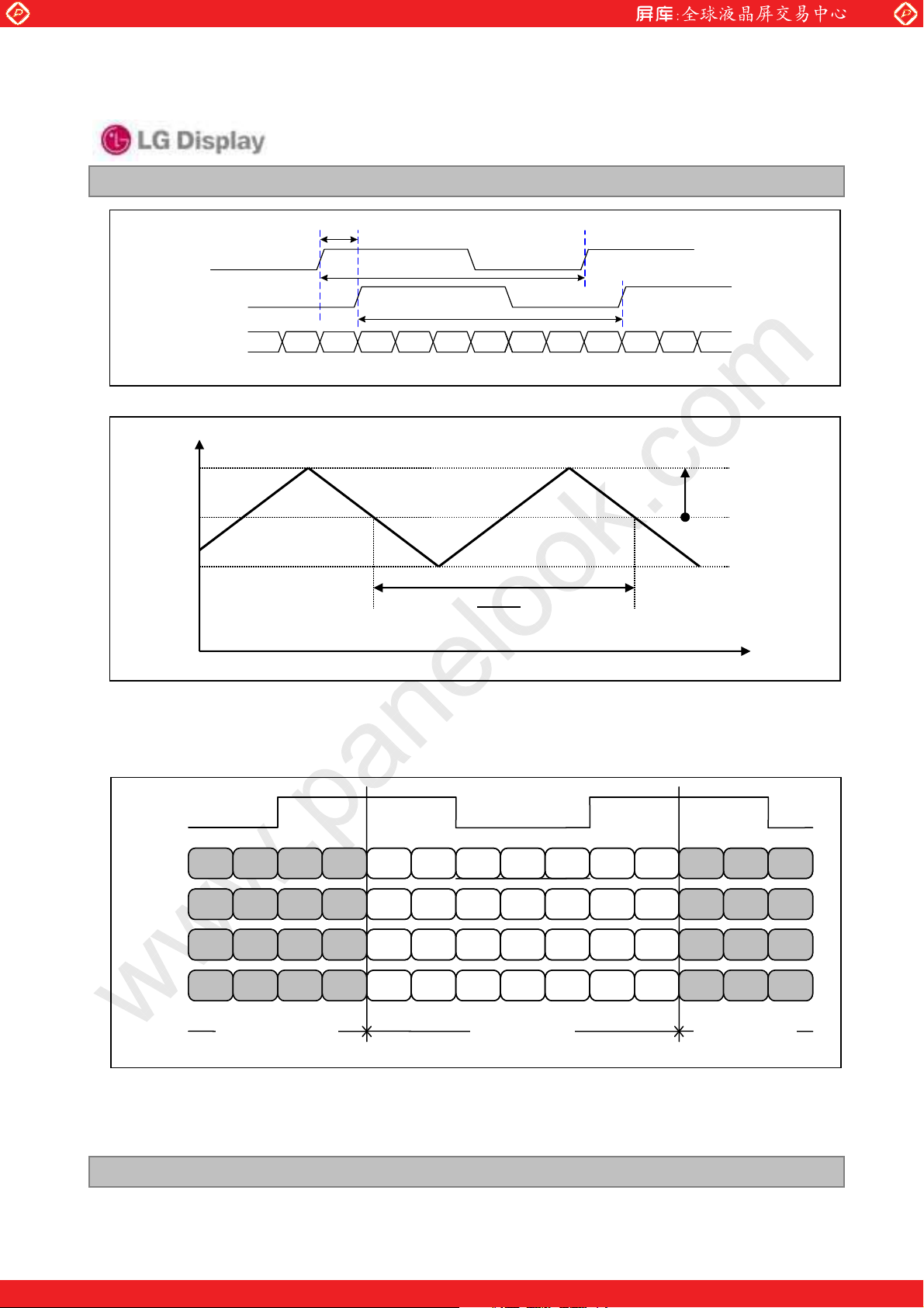
Global LCD Panel Exchange Center
t
SKEW_EO
www.panelook.com
LP141WX3
Liquid Crystal Display
Product Specification
LVDS Odd Clock
LVDS Even Clock
LVDS Even Data
Freq.
F
max
F
center
F
min
T
clk
T
clk
< Clock skew ma rgin between channel >
X
m
tvk
< Spread Spectrum >
m
QGm
Time
kl}
3-3-3. Data Format
1) LVDS 1 Port
RCLK+
RA+/-
RB+/-
RC+/-
RD+/-
R3 R2
G4 G3
B5 B4
G7 G6
Previous (N-1)th Cycle Next(N+1)th Cycle
R1 R0
G2 G1
B3 B2
R7 R6
Ver. 1.0 Nov. 25, 2009
G0 R5 R4 R3 R2 R1 R0
B1 B0 G5 G4 G3 G2 G1
DE VSYNCHSYNC B5 B4 B3 B2
X B7 B6 G7 G6 R7 R6
Current(Nth) Cycle
< LVDS Da ta Form a t >
G0
R5 R4
B1
B0 G5
DE
VSYNCHSYNC
X
B7 B6
10 / 31
One step solution for LCD / PDP / OLED panel application: Datasheet, inventory and accessory!
www.panelook.com
Page 11

Global LCD Panel Exchange Center
3-4. Signal Timing Specifications
This is the sig nal timing required at the input of the User connec to r. All of the interface signal timing should be
satisfied with the f ollowing specif ications and s pecificatio ns of LVDS Tx/Rx f or its proper op eration.
ITEM Symbol Min Typ Max Unit Note
www.panelook.com
LP141WX3
Liquid Crystal Display
Product Specification
Table 6. TIMING TABLE
DCLK Frequency f
CLK
- 69.3 - MHz
Hsync Period Thp 1360 1405 1480
16 32 48
1280 1280 1280
809 822 860
2610
800 800 800
40 45 96
24 48 56
61332
1318
Width-Active t
Vsync Period t
Width-Active t
Data
Enable
Horizontal back porch t
Horizontal front porch t
Vertical back porch t
Vertical front p orch t
WH
WHA
VP
WV
WVA
HBP
HFP
VBP
VFP
3-5. Signal Timing Waveforms
DataEnable, Hsync, Vsync
tCLK
DCLK
0.5 Vcc
Hig h: 0.7VCC
Low: 0.3VCC
tCLKWidth t
tHPWidth t
tCLK
tHP
Condition: VCC=3.3V
t
HP
Hsync
t
WH
t
HBP
tWHA
t
HFP
Data Enable
t
VP
t
WV
Vsync
t
VBP
tWVA
t
VFP
Data Enable
Ver. 1.0 Nov. 25, 2009
One step solution for LCD / PDP / OLED panel application: Datasheet, inventory and accessory!
11 / 31
www.panelook.com
Page 12

Global LCD Panel Exchange Center
3-6. Color Input Data Reference
The brightness of each primary color (red,green and blue) is based on the 6-bit gray scale data input for the
co lor ; the hig her the binary input, the b righter the co lo r. The tab le below provides a ref erence f or color
versus data input.
www.panelook.com
LP141WX3
Liquid Crystal Display
Product Specification
Table 7. COLOR DATA REFERENCE
Input Color Data
Basic
Color
RED
GREEN
BLUE
Color
Black
Red
Green
Blue
Cyan
Magenta
Yellow
White
RED (00)
RED (0 1)
…
RED (6 2)
RED (6 3)
GREEN (00)
GREEN (01)
...
GREEN (62)
GREEN (63)
BLUE (00 )
BLUE (01)
…
BLUE (62 )
BLUE (63 )
RED
MSB LSB
R5 R4 R3 R2 R1 R0 G 5 G 4 G3 G 2 G 1 G0 B5 B4 B3 B2 B1 B0
000000000000000000
111111000000000000
000000111111000000
000000000000111111
000000111111111111
111111000000111111
111111111111000000
111111111111111111
000000000000000000
000001000000000000
…… …
111110000000000000
111111000000000000
000000000000000000
000000000001000000
…… …
000000111110000000
000000111111000000
000000000000000000
000000000000000001
…… …
000000000000111110
000000000000111111
MSB LSB
GREEN
BLUE
MSB LSB
Ver. 1.0 Nov. 25, 2009
One step solution for LCD / PDP / OLED panel application: Datasheet, inventory and accessory!
12 / 31
www.panelook.com
Page 13

Global LCD Panel Exchange Center
3-7. Power Sequence
www.panelook.com
LP141WX3
Liquid Crystal Display
Product Specification
Power Supply For LCD
VCC
Interface Signal,
V
i
(LVDS Signal of Transmitter)
LAMP Power
Parameter Value Units
90%
0V
T
T
1
2
Valid Data
0V
T
3
Table 8. POWER SE QUENCE TABLE
90%
10%10%
T
T
6
5
T
4
T
7
OFFOFF LAMP ON
Min. Typ. Max.
T
1
T
2
T
3
T
4
T
5
T
6
T
7
0.5 - 10 (ms)
0 - 50 (ms)
200 - - (ms)
200 - - (ms)
0 - 50 (ms)
0 - 10 (ms)
200 - - (ms)
Note)
1. Valid Data is Data to meet “3-3. LVDS Signal Timing Specifications”
2. Please avoid f lo ating s tate of interf ace sig nal at invalid perio d.
3. When the interf ace signal is invalid, be s ure to pull do wn the po wer sup ply for LCD VCC to 0V.
4. Lamp power must be turn on af ter power supply f or LCD and interface sig nal are valid.
Ver. 1.0 Nov. 25, 2009
13 / 31
One step solution for LCD / PDP / OLED panel application: Datasheet, inventory and accessory!
www.panelook.com
Page 14

Global LCD Panel Exchange Center
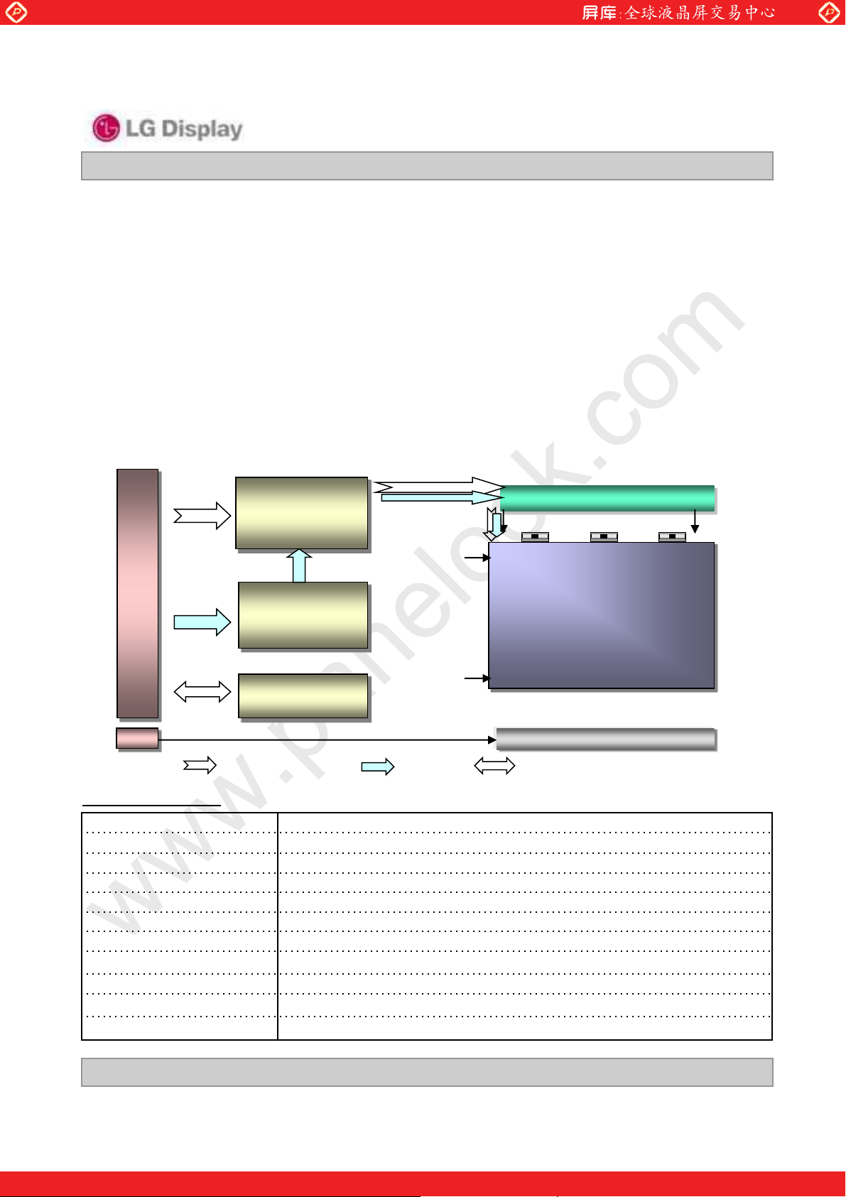
4. Optical Specification
Optical characteristics are determined af ter the unit has b een ‘ON’ and stable for approximately 30 minutes in
a d ark environment at 25qC. The values sp ecif ied are at an ap proximate distance 50cm f rom the LCD surf ace
at a viewing angle of ) and 4 equal to 0q.
FIG. 1 presents additional inf ormatio n concerning the measurement equipment and metho d.
FIG. 1 Optical Characteristic Measurement Equipment and Method
www.panelook.com
LP141WX3
Liquid Crystal Display
Product Specification
Optical Stage(x,y)
LCD Module
Pritchard 880 or
equivalent
50cm
Table 9. OPTICAL CHARACTERISTICS
Ta=25qC , VCC=3.3V, f V=60Hz, f
Param eter Symbol
Contrast Ratio CR 300 - - 1
Surface Luminance, white L
Luminance Variation G
Response Time
Color Coordinates
RED RX 0.554 0.584 0.614
GREEN GX 0.294 0.324 0.354
BLUE BX 0.128 0.158 0.188
WHITE WX 0.283 0.313 0.343
Viewing Angle 5
x axis, right()=0q) 4r 40 - - degree
x axis, left ()=180q) 4l 40 - - degree
y axis, up ()=90q) 4u 15 - - degree
y axis, down ()=270q) 4d 35 - - degree
Gray Scale 6
WH
WHITE
TrR+ Tr
RY 0.317 0.347 0.377
GY 0.512 0.542 0.572
BY 0.115 0.145 0.175
WY 0.299 0.329 0.359
Min Typ Max
170 200 - cd/m
-1.41.6 3
D
Values
16 ms 4
= 69.3MHz, F
CLK
55kHz , IBL= 6.0mA
BL
=
Units Notes
2
2
Ver. 1.0 Nov. 25, 2009
One step solution for LCD / PDP / OLED panel application: Datasheet, inventory and accessory!
14 / 31
www.panelook.com
Page 15

Global LCD Panel Exchange Center
Note)
1. Contrast Ratio (CR) is d ef ined mathematically as
Surf ace Luminance with all white p ixels
Contrast Rat io =
Surf ace Luminance with all black pixels
2. Surface luminance is the average of 5 point across the LCD surf ace 50cm f rom the surf ace with
all pixels disp laying white. For mo re inf ormatio n see FIG 1.
= Average(L1,L2, … L5)
L
WH
3. The variation in surface luminance , The panel total variatio n (
at each test po sitio n 1 through 13 and then defined as f ollowed numerical formula.
For more inf ormation see FIG 2.
www.panelook.com
Product Specification
Liquid Crystal Display
G
) is determined by measuring L
WHITE
LP141WX3
N
1,L2
, … L13)
G
WHITE
Maximum(L
=
Minimum(L1,L2, … L13)
4. Response time is the time required for the display to transition from white to black (rise time, Tr
) and
R
from black to white(Decay Time, TrD). For ad ditional informatio n see FIG 3.
5. Viewing angle is the angle at which the contrast ratio is greater than 10. The angles are d etermined
f or the horizontal or x axis and the vertical o r y axis with respect to the z axis which is normal to the
LCD surf ace. For more information see FIG 4.
6. Gray scale specification * f
= 60Hz
V
Gray Level Luminance [%] (Typ )
L0
L7
L15
L23
L31
L39
L47
L55
L63
࣮࣬࣪
ࣲ࣭࣪ࣵ
ࣰࣲ࣪
ࣲ࣭࣮࣪
ࣰ࣮࣬࣪
ࣰ࣯࣪ࣵ
ࣱࣱ࣮࣪
ࣳࣴ࣪ࣴ
࣭࣬࣬
Ver. 1.0 Nov. 25, 2009
One step solution for LCD / PDP / OLED panel application: Datasheet, inventory and accessory!
15 / 31
www.panelook.com
Page 16

Global LCD Panel Exchange Center
FIG. 2 Luminance
<measuring point f or surf ace luminance & measuring point f or luminance variation>
www.panelook.com
LP141WX3
Liquid Crystal Display
Product Specification
H
A
C
L6
L2
L7
L3
B
V
L9
L1
D
L8
L10
H,V : ACTIVE AREA
A : H/4 mm
B : V/4 mm
C : 10 mm
D : 10 mm
POINTS : 13 POINTS
Center Point
L4 L5
L11 L13
FIG. 3 Response Time
The resp onse time is defined as the following f ig ure and shall be measured by switching the input signal
for “black” and “white”.
L12
Tr
Tr
%
100
90
Optical
Response
Ver. 1.0 Nov. 25, 2009
10
0
white
R
black
D
white
One step solution for LCD / PDP / OLED panel application: Datasheet, inventory and accessory!
16 / 31
www.panelook.com
Page 17

Global LCD Panel Exchange Center
5. Mechanical Characteristics
The co ntents provide general m echanical characte ristics fo r the mo del LP141WX3. In ad dition the f igures
in the next pag e are detailed mechanical drawing of the LCD.
www.panelook.com
LP141WX3
Liquid Crystal Display
Product Specification
Horizontal 319.5 r 0.5mm
Outline Dimension
Bezel Are a
Active Display Area
Weight 400(Max)
Surface Treatment
Vertical 205.5 r 0.5mm
Thickness 5.5m m (m ax)
Horizontal 306.76 r 0.5mm
Vertical 193.00 r 0.5mm
Horizontal 303.74 mm
Vertical 189.84 mm
Glare treatment of the front polarizer
Ver. 1.0 Nov. 25, 2009
One step solution for LCD / PDP / OLED panel application: Datasheet, inventory and accessory!
17 / 31
www.panelook.com
Page 18

Global LCD Panel Exchange Center
www.panelook.com
LP141WX3
Liquid Crystal Display
Product Specification
<FRONT VIEW>
Wire Length : 61mm
Note) Unit:[mm], General tolerance:
r 0.5mm
Ver. 1.0 Nov. 25, 2009
One step solution for LCD / PDP / OLED panel application: Datasheet, inventory and accessory!
18 / 31
www.panelook.com
Page 19

Global LCD Panel Exchange Center
www.panelook.com
LP141WX3
Liquid Crystal Display
Product Specification
<REAR VIEW>
Note) Unit:[mm], General tolerance:
r 0.5mm
Ver. 1.0 Nov. 25, 2009
One step solution for LCD / PDP / OLED panel application: Datasheet, inventory and accessory!
19 / 31
www.panelook.com
Page 20

Global LCD Panel Exchange Center
[ DETAIL DESCRIPTION OF SIDE MOUNTING SCREW ]
www.panelook.com
LP141WX3
Liquid Crystal Display
Product Specification
* Mo unting Screw Length (A)
= 1.8(Min) / 2.5(Max)
* Mo unting Screw Hole Depth (B)
= 2.5(Max)
* Mo unting hole location : 3.1(typ.)
* Torque : 2.5 kgf .cm(Max)
(Measurement gauge : torque meter)
Notes : 1. Screw plated through the method of non-electrolytic nickel plating is preferred
to reduce possibility that results in vertical and/or horizontal line defect due to
the conductive particles from screw surf ace.
Ver. 1.0 Nov. 25, 2009
One step solution for LCD / PDP / OLED panel application: Datasheet, inventory and accessory!
20 / 31
www.panelook.com
Page 21

Global LCD Panel Exchange Center
LPL Proposal for system cover design.(Appendix)
www.panelook.com
LP141WX3
Liquid Crystal Display
Product Specification
1
Gap check for securing the enough gap between LCM
and System cover.
1.Rear side of LCM is sensitive against external stress,and previous check
about interference is highly needed.
Define
2.In case there is something from system cover comes into the boundary
above,mechanical interference may cause the FOS defects.
(Eg:Ripple,White spot..)
2 Check if antenna cable is sufficiently apart from T-CON of LCD Module.
Define
NO GOOD
GOOD
1.If system antenna is overlapped with T-CON,it might be cause the noise.
Ver. 1.0 Nov. 25, 2009
21 / 31
One step solution for LCD / PDP / OLED panel application: Datasheet, inventory and accessory!
www.panelook.com
Page 22

Global LCD Panel Exchange Center
LPL Proposal for system cover design.
www.panelook.com
LP141WX3
Liquid Crystal Display
Product Specification
3
Define
Gap check for securing the enough gap between LCM
and System hinge.
1.At least 2.0mm of gap needs to be secured to prevent the shock
related defects.
2.”L” type of hinge is recommended than “I” type under shock test.
4
Checking the path of the System wire.
#4#5#6
Good
Ok
Bad
1.COF area needs to be handled with care.
2.GOOD ÎWire path design to system side.
Define
OKÎ Wire path is located between COFs.
BADÎWire path overlapped with COF area.
Ver. 1.0 Nov. 25, 2009
#3
#2
#1
22 / 31
One step solution for LCD / PDP / OLED panel application: Datasheet, inventory and accessory!
www.panelook.com
Page 23

Global LCD Panel Exchange Center
LPL Proposal for system cover design.
5 Using a bracket on the top of LCM is not recommended.
bracket
www.panelook.com
LP141WX3
Liquid Crystal Display
Product Specification
With bracket Without bracket
1.Condition without bracket is good for mech anical noise,and can minimize
the light leakage from deformation of bracket.
Define
2.The results shows that there is no difference between the condition
with or without bracket.
6 Securing additional gap on CNT area..
A
A~A-1
cut
System co ver inner side.
User connector
area.
A-1
User connector
Cable pathway.
FPC:Flexible Printed Circuit.
1.CNT area is specially sensitive against external stress,and additional
Define
gap by cutting on system cover will be helpful on removing the Ripple.
2.Using a thinner CNT will be better. (eg: FPC type)
Ver. 1.0 Nov. 25, 2009
One step solution for LCD / PDP / OLED panel application: Datasheet, inventory and accessory!
23 / 31
www.panelook.com
Page 24

Global LCD Panel Exchange Center
6. Reliability
Environment test condition
No. Test Item Cond itions
1 Hig h temperature storag e test Ta= 60qC, 240h
2 Low temp erature storage test Ta= -20qC, 240h
3 Hig h temperature operation test Ta= 50qC, 50%RH, 240h
4 Low temp erature operatio n test Ta= 0qC, 240h
www.panelook.com
LP141WX3
Liquid Crystal Display
Product Specification
5 Vibration test (no n-op erating) Sine wave, 10 ~ 500 ~ 10Hz, 1.5G, 0.37oct/min
3 axis, 1hour/axis
6 Shock test (non-operating) Half sine wave, 180G, 2ms
one shock of each six f aces(I.e. run 180G, 2ms
for all six faces)
7 Altitude operating
storag e / shipment
{ Result Evaluation Criteria }
There should b e no change which might af f ect the practical disp lay function when the display q uality
test is co nducted und er normal op erating cond ition.
0 ~ 10,000 f eet (3,048m) 24Hr
0 ~ 40,000 f eet (12,192m) 24Hr
Ver. 1.0 Nov. 25, 2009
One step solution for LCD / PDP / OLED panel application: Datasheet, inventory and accessory!
24 / 31
www.panelook.com
Page 25

Global LCD Panel Exchange Center
7. International Standards
7-1. Safety
a) UL 60950-1, Seco nd Edition, Underwriters Labo rato ries Inc.
Information Technology Equipment - Saf ety - Part 1 : General Requirements.
b) CAN/CSA C22.2 No.60950-1-07, Seco nd Edition, Canadian Stand ards Association.
Information Technology Equipment - Saf ety - Part 1 : General Requirements.
c) EN 60950-1:2006 + A11:2009, Europ ean Committee f or Electro technical Standard ization (CENELEC).
Information Technology Equipment - Saf ety - Part 1 : General Requirements.
d) IEC 60950-1:2005, Second Edition, The International Electrotechnical Co mmission (IEC).
Information Technology Equipment - Saf ety - Part 1 : General Requirements.
www.panelook.com
LP141WX3
Liquid Crystal Display
Product Specification
7-2. EMC
a) ANSI C63.4 “American National Standard for Methods of Measurement of Radio-Noise
Emissions from Low-Voltage Electrical and Electronic Equipment in the Range of 9 kHz to 40 GHz.”
American National Standards Institute (ANSI), 2003.
b) CISPR 22 “Information technology equipment – Radio disturbance characteristics – Limit and
methods of measurement." International Special Committee on Radio Interference
(CISPR), 2005.
c) CISPR 13 “Sound and television broadcast receivers and associated equipment – Radio disturbance
characteristics – Limits and method of measurement." International Special Committee on Radio
Interference (CISPR), 2006.
7-3. Environment
a) RoHS, Directive 2002/95/EC of the European Parliament and of the council of 27 January 2003
Ver. 1.0 Nov. 25, 2009
One step solution for LCD / PDP / OLED panel application: Datasheet, inventory and accessory!
25 / 31
www.panelook.com
Page 26

Global LCD Panel Exchange Center
8. Packing
8-1. Designation of Lot Mark
a) Lot Mark
ABCDEFGHI JKLM
A,B,C : SIZE(INCH) D : YEAR
E : MONTH F ~ M : SERIAL NO.
www.panelook.com
LP141WX3
Liquid Crystal Display
Product Specification
Note
1. YEAR
Year
Mark
321
200452005
4
200320022001
2006720078200892009
6
2. MONTH
Month
Mark
Apr5May
4
Jun7Jul8Aug9Sep
6
b) Location of Lot Mark
Serial No. is printed on the lab el. The label is attached to the backside of the LCD mo dule.
This is s ubject to chang e witho ut prior notice.
8-2. Packing Form
a) Package quantity in one box : 22 pcs
b) Box Size : 389mm Ý 345mm Ý 288mm
2010
0
Oct
A
Nov
B
DecMarFebJan
C321
Ver. 1.0 Nov. 25, 2009
One step solution for LCD / PDP / OLED panel application: Datasheet, inventory and accessory!
26 / 31
www.panelook.com
Page 27

Global LCD Panel Exchange Center
9. PRECAUTIONS
Pleas e pay attention to the f ollo wings when you use this TFT LCD module.
9-1. MOUNTING PRECAUT IONS
(1) You must mount a module using holes arranged in f our corners or f our sides.
(2) You sho uld consider the mo unting structure so that uneven force (ex. Twisted stress) is not applied to
the
module. And the case o n which a mod ule is mounted should have sufficient strength so that external
force is not transmitted directly to the module.
(3) Please attach the surface transparent protective plate to the s urf ace in o rder to p rotect the p olarizer.
Transparent protective plate should hav e suf f ic ient streng th in ord er to the resist external f orce.
(4) You should adopt radiation structure to satisfy the temperature specification.
(5) Acetic acid type and chlorine type materials f or the cover case are not d esirable b ecause the f ormer
generates corros ive gas of attacking the po larizer at high temperature and the latter causes circuit break
by electro-chemical reaction.
(6) Do not touch, p ush o r rub the exposed polarizers with glass, tweezers o r anything harder than HB
pencil lead . And p lease do not rub with dust clothes with chemical treatment.
Do no t touch the surface of po larizer f or b are hand o r greasy cloth.(Some cosmetics are detrimental
to the polarizer.)
(7) Whe n the surf ace becomes dusty, please wipe gently with ab sorbent cotto n or other sof t materials like
chamois so aks with p etroleum benzene. Normal-hexane is recommended for cleaning the adhesives
used to attach front / rear p olarizers. D o not use acetone, toluene and alcoho l because they cause
chemical damage to the p olarizer.
(8) Wipe off saliva or water drops as soon as possible. Their long time contact with polarizer causes
deformations and co lo r f ading.
(9) D o not op en the case because insid e circuits do not have suf ficient strength.
www.panelook.com
LP141WX3
Liquid Crystal Display
Product Specification
9-2. OPERATING PRECAUT IONS
(1) The spike noise causes the mis -operation of circuits. It should be lower than f ollowing voltag e :
V=· 200mV(Over and under shoot voltage)
(2) Respons e time depend s on the temperature.(In lo wer temp erature, it b eco mes longer.)
(3) Brig htness dep ends on the temperature. (In lower temperature, it bec omes lower.)
And in lower temperature, response time(required time that brightness is stable after turned on) becomes
longer.
(4) Be ca ref ul for condensation at sudd en temperature change. Condensatio n makes damag e to polarizer or
electrical contacted parts. And after fading condensation, smear or spot will occur.
(5) When fixed patterns are displayed f or a long time, remnant image is likely to occur.
(6) Mod ule has high f requency circuits. Sufficient suppression to the electromagnetic interf erence shall be
done by system manuf acturers. Grounding and shielding method s may b e impo rtant to minimized the
interference.
Ver. 1.0 Nov. 25, 2009
27 / 31
One step solution for LCD / PDP / OLED panel application: Datasheet, inventory and accessory!
www.panelook.com
Page 28

Global LCD Panel Exchange Center
9-3. ELECTROSTATIC DISCHARGE CONTROL
Sinc e a module is composed of electronic circuits, it is not strong to electrostatic discharge. Make certain that
treatment persons are connected to g round through wrist band etc. And don’t touch interf ace pin directly.
9-4. PRECAUTIONS FOR STRONG LIGHT EXPOSURE
Strong lig ht ex posure causes degrad ation o f polarizer and color f ilter.
9-5. STORAGE
www.panelook.com
LP141WX3
Liquid Crystal Display
Product Specification
When storing modules as spares f or a lo ng time, the f ollo wing precautio ns are necess ary.
(1) Store th em in a dark place. Do not exp ose the module to sunlight o r f luorescent lig ht. Keep the
temperature between 5qC and 35qC at normal humidity.
(2) The polarizer surface sho uld not come in contact with any other ob ject.
It is recommend ed that they be s to red in the container in which they were shipp ed.
9-6. HANDLING PRECAUTIONS FOR PROTECT ION FILM
(1) When the pro tection f ilm is peeled of f , static electricity is g enerated between the f ilm and p olarizer.
This should b e peeled of f slowly and carefully b y peo ple who are electrically grounded and with well
ion-blown equipment or in s uch a conditio n, etc.
(2) The p rotection film is attached to the polarizer with a small amount of glue. If some stress is ap plied
to rub the protection film ag ainst the po larizer during the time yo u peel o f f the film, the g lue is apt to
remain o n the polarizer.
Pleas e caref ully peel of f the pro tection f ilm witho ut rubbing it ag ainst the p olarizer.
(3) When the module with protection film attached is stored f or a long time, so metimes there remains a
very small amount of glue still on the polarizer after the protection film is peeled of f .
(4) You can remove the glue easily. When the glue remains o n the po larizer surf ace or its vestig e is
reco gnized, please wipe them o f f with abs orbent cotton waste or other soft material like chamois
so aked with normal-hexane.
Ver. 1.0 Nov. 25, 2009
One step solution for LCD / PDP / OLED panel application: Datasheet, inventory and accessory!
28 / 31
www.panelook.com
Page 29

Global LCD Panel Exchange Center
Byte
(Dec)
Byte
(Hex)
Field Name and Comments
Value
(Hex)
Value
(Bin)
0 00 Header
00
00000000
1 01 Header
FF
11111111
2 02 Header
FF
11111111
3 03 Header
FF
11111111
4 04 Header
FF
11111111
5 05 Header
FF
11111111
6 06 Header
FF
11111111
7 07 Header
00
00000000
8 08 EISA man ufact ure co de ( 3 Charac ter ID ) LGD
30
00110000
9 09 EISA manufacture code (Compressed ASCซ)
E4
11100100
10 0A Panel Supplier Reserved - Product Code 027Eh
7E
01111110
11 0B ( He x. LSB first )
02
00000010
12 0C LCD Module Serial No - Preferred but Optional ("0" If not used)
00
00000000
13 0D LCD Module Serial No - Preferred but Optional ("0" If not used)
00
00000000
14 0E LCD Module Serial No - Preferred but Optional ("0" If not used)
00
00000000
15 0F LCD Module Serial No - Preferred but Optional ("0" If not used)
00
00000000
16 10 Week of M anufacture 00 weeks
00
00000000
17 11 Year o f Man ufacture 2009 years
13
00010011
18 12 EDID structure version # = 1
01
00000001
19 13 EDID revision # = 3
03
00000011
20 14 Video input Definition = Digital signal
80
10000000
21 15 Max H image size (Rounded cm) = 30 cm
1E
00011110
22 16 Max V image size (Rounded cm) = 19 cm
13
00010011
23 17 Displa y gamma = (g amma* 100)-100 = Example:(2.2*100)-100=120 = 2.2 Gamma
78
01111000
24 18
Feature Support (no_DPMS, no_Active Off/Very Low Power, RGB color display, Timing BLK 1,no_ GTF)
0A
00001010
25 19 Red / Gree n Low Bit s (RxRy / GxGy )
B3
10110011
26 1A Blue/White Low Bits (BxBy/WxWy)
85
10000101
27 1B Red X Rx = 0.584
95
10010101
28 1C Red Y Ry = 0.347
58
01011000
29 1D Green X Gx = 0.324
53
01010011
30 1E Gr ee n Y Gy = 0 .54 2
8A
10001010
31 1F Blue X Bx = 0.158
28
00101000
32 20 Blue Y By = 0.145
25
00100101
33 21 Whit e X Wx = 0.313
50
01010000
34 22 Whit e Y Wy = 0.329
54
01010100
35 23 Es tablished timing 1 (00h if not used)
00
00000000
36 24 Es tablished timing 2 (00h if not used)
00
00000000
37 25 Manufacturer's timings (00h if not used)
00
00000000
38 26 Standard timing ID1 (01h if not used)
01
00000001
39 27 Standard timing ID1 (01h if not used)
01
00000001
40 28 Standard timing ID2 (01h if not used)
01
00000001
41 29 Standard timing ID2 (01h if not used)
01
00000001
42 2A Standard timing ID3 (01h if not used)
01
00000001
43 2B Standard timing ID3 (01h if not used)
01
00000001
44 2C Standard timing ID4 (01h if not used)
01
00000001
45 2D Standard timing ID4 (01h if not used)
01
00000001
46 2E Standard timing ID5 (01h if not used)
01
00000001
47 2F Standard timing ID5 (01h if not used)
01
00000001
48 30 Standard timing ID6 (01h if not used)
01
00000001
49 31 Standard timing ID6 (01h if not used)
01
00000001
50 32 Standard timing ID7 (01h if not used)
01
00000001
51 33 Standard timing ID7 (01h if not used)
01
00000001
52 34 Standard timing ID8 (01h if not used)
01
00000001
53 35 Standard timing ID8 (01h if not used)
01
00000001
Vendor / Product EDID
Version
Display
Parameters
Panel Color Coordinates
Establ
ished
Timin
APPENDIX A. Enhanced Extended Display Identification Data (EEDIDTM) 1/3
Header
www.panelook.com
LP141WX3
Liquid Crystal Display
Product Specification
One step solution for LCD / PDP / OLED panel application: Datasheet, inventory and accessory!
Standard Timing ID
Ver. 1.0 Nov. 25, 2009
29 / 31
www.panelook.com
Page 30

Global LCD Panel Exchange Center
Byte
(Dec)
Byte
(Hex)
Field Name and Comments
Value
(Hex)
Value
(Bin)
54 36 Pixel Cloc k/10,000 (LSB) 69.3 MHz @ 60Hz
12
00010010
55 37 Pixel Cloc k/10,000 (MSB)
1B
00011011
56 38 Horizon tal Ac tive (lower 8 b its) 1280 Pixels
00
00000000
57 39 Horizon tal Blan king(T hp-HA ) (lower 8 b its) 125 Pixels
7D
01111101
58 3A Horizontal Active / Horizontal Blanking(Thp-HA) (upper 4:4bits)
50
01010000
59 3B Vertica l Av tive 800 Lin es
20
00100000
60 3C Vertical Blanking (Tvp-HA) (DE Blanking typ.fo r DE only pane ls) 22 Lines
16
00010110
61 3D Vertical Active : Vertical Blanking (Tvp-HA) (upper 4:4bits)
30
00110000
62 3E Ho rizont al Sync. Offset (Thfp) 48 Pixels
30
00110000
63 3F Horizon tal Syn c Pulse Width (HSPW) 32 Pixels
20
00100000
64 40 Vertical Sync Offse t(Tvfp) : Syn c Width (VSPW) 3 Lines : 6 Lines
36
00110110
65 41 Horizontal Vertical Sync Offset/Width (upper 2bits)
00
00000000
66 42 Horizon tal Image Size (mm) 304 mm
30
00110000
67 43 Vertical Imag e Size (mm) 190 mm
BE
10111110
68 44 Horizontal Image Size / Vertical Image Size
10
00010000
69 45 Horizontal Border = 0 (Zero for Notebook LCD)
00
00000000
70 46 Vertical Border = 0 (Zero for Notebook LCD)
00
00000000
71 47
Non-Interlace, Normal display, no stereo, Digital Separate ( Vsync_NEG, Hsync_NEG )
18
00011000
72 48 Flag
00
00000000
73 49 Flag
00
00000000
74 4A Flag
00
00000000
75 4B Data Type Tag (Descriptor Defined by manufacturer )
00
00000000
76 4C Flag
00
00000000
77 4D Descriptor Defined by manufacturer
00
00000000
78 4E Descriptor Defined by manufacturer
00
00000000
79 4F Descriptor Defined by manufacturer
00
00000000
80 50 Descriptor Defined by manufacturer
00
00000000
81 51 Descriptor Defined by manufacturer
00
00000000
82 52 Descriptor Defined by manufacturer
00
00000000
83 53 Descriptor Defined by manufacturer
00
00000000
84 54 Descriptor Defined by manufacturer
00
00000000
85 55 Descriptor Defined by manufacturer
00
00000000
86 56 Descriptor Defined by manufacturer
00
00000000
87 57 Descriptor Defined by manufacturer
00
00000000
88 58 Descriptor Defined by manufacturer
00
00000000
89 59
Descriptor Defined by manufacturer
00
00000000
90 5A Flag
00
00000000
91 5B Flag
00
00000000
92 5C Flag
00
00000000
93 5D Dat a Type Tag ( ASCII String )
FE
11111110
94 5E Flag
00
00000000
95 5F ASCII String L
4C
01001100
96 60 ASCII String G
47
01000111
97 61 ASCII String
20
00100000
98 62 ASCII String D
44
01000100
99 63 ASCII String i
69
01101001
100 64 ASCII Strin g s
73
01110011
101 65 ASCII Strin g p
70
01110000
102 66 ASCII Strin g l
6C
01101100
103 67 ASCII Strin g a
61
01100001
104 68 ASCII Strin g y
79
01111001
105 69
Man ufact urer P/N(If<13 ch ar--> 0Ah, t hen t ermina te with ASCซ cod e 0Ah,s et remaining char = 20h)
Man ufact urer P/N(If<13 ch ar--> 0Ah, t hen t ermina te with ASCซ cod e 0Ah,s et remaining char = 20h)
APPENDIX A. Enhanced Extended Display Identification Data (EEDIDTM) 2/3
www.panelook.com
LP141WX3
Liquid Crystal Display
Product Specification
One step solution for LCD / PDP / OLED panel application: Datasheet, inventory and accessory!
Timing Descriptor #1Timing Descriptor #2Timing Descriptor #3
106 6A
107 6B M anufactu rer P/N(If<13 char--> 0Ah, then terminate with ASCซ code 0Ah,set remaining char = 20h)
Ver. 1.0 Nov. 25, 2009
00001010
0A
00100000
20
00100000
20
30 / 31
www.panelook.com
Page 31

Global LCD Panel Exchange Center
Byte
(Dec)
Byte
(Hex)
Field Name and Comments
Value
(Hex)
Value
(Bin)
108 6C Flag
00
00000000
109 6D Flag
00
00000000
110 6E Flag
00
00000000
111 6F Data Ty pe Tag ( ASCII St ring )
FE
11111110
112 70 Flag
00
00000000
113 71 ASCII String L
4C
01001100
114 72 ASCII String P
50
01010000
115 73 ASCII String 1
31
00110001
116 74 ASCII String 4
34
00110100
117 75 ASCII String 1
31
00110001
118 76 ASCII String W
57
01010111
119 77 ASCII String X
58
01011000
120 78 ASCII String 3
33
00110011
121 79 ASCII String -
2D
00101101
122 7A ASCII String T
54
01010100
123 7B A SCII String L
4C
01001100
124 7C ASCII String N
4E
01001110
125 7D ASCII String 4
34
00110100
126 7E Extens ion flag (# of option al 128 panel ID e xten sion blo ck to follo w, Typ = 0)
00
00000000
127 7F Check Sum (Th e 1-byte sum of all 128 by tes in this pan el ID blo ck sh all = 0)
F7
11110111
APPENDIX A. Enhanced Extended Display Identification Data (EEDIDTM) 3/3
www.panelook.com
LP141WX3
Liquid Crystal Display
Product Specification
Checksum Timing Descriptor #4
Ver. 1.0 Nov. 25, 2009
31 / 31
One step solution for LCD / PDP / OLED panel application: Datasheet, inventory and accessory!
www.panelook.com
 Loading...