

Page 1
Product Specification
1 / 27
LP140WH1
Liquid Crystal Display
Ver. 1.0 Oct.09, 2009
SPECIFICATION
FOR
APPROVAL
14.0”W HD TFT LCDTitle
MODEL
HPCustomer
*When you obtain standard approval,
please use the above model name without suffix
LP140WH1*MODEL
TLD3Suffix
LG Display Co., Ltd.SUPPLIER
)
)
(
(
Final Specification
Preliminary Specification
◆
Please return 1 copy for your confirmation with
your signature and comments.
/
/
/
SIGNATUREAPPROVED BY
PREPARED BY
REVIEWED BY
SIGNATURE
APPROVED BY
K. J. Kwon / S.Manager
Products Engineering Dept.
LG Display Co., Ltd
PREPARED BY
REVIEWED BY
SIGNATURE
APPROVED BY
M.J. Lee / Manager
J.Y.Lee / Engineer
C.H.Lee / Engineer
Page 2
Product Specification
2 / 27
LP140WH1
Liquid Crystal Display
Ver. 1.0 Oct.09, 2009
Contents
9-10
LVDS SIGNAL TIMING SPECIFICATION 3-3
26-28
APPENDIX. Enhanced Extended Display Identification Data A
24-25
PRECAUTIONS9
12
8
INTERFACE CONNECTIONS 3-2
COLOR INPUT DATA REFERNECE 3-5
23
DESIGNATION OF LOT MARK 8-1
23
PACKING FORM 8-2
PACKING8
22
EMC 7-2
1
COVER
2
CONTENTS
3
RECORD OF REVISIONS
4
GENERAL DESCRIPTION1
5
ABSOLUTE MAXIMUM RATINGS2
ELECTRICAL SPECIFICATIONS3
6
ELECTRICAL CHARACTREISTICS 3-1
10
SIGNAL TIMING SPECIFICATIONS 3-3
11
SIGNAL TIMING WAVEFORMS 3-4
13
POWER SEQUENCE 3-6
14-16
OPTICAL SFECIFICATIONS4
17-20
MECHANICAL CHARACTERISTICS5
21
RELIABLITY6
INTERNATIONAL STANDARDS7
22
SAFETY 7-1
Page
ITEMNo
Page 3
Product Specification
3 / 27
LP140WH1
Liquid Crystal Display
Ver. 1.0 Oct.09, 2009
RECORD OF REVISIONS
0.1EDID Update26~28Aug. 13. 20090.2
1.0 Final CAS-Oct. 09. 20091.0
0.0
EDID
ver
First Draft (Preliminary Specification)-Jun. 16, 20090.0
DescriptionPageRevision DateRevision No
Page 4
Product Specification
4 / 27
LP140WH1
Liquid Crystal Display
Ver. 1.0 Oct.09, 2009
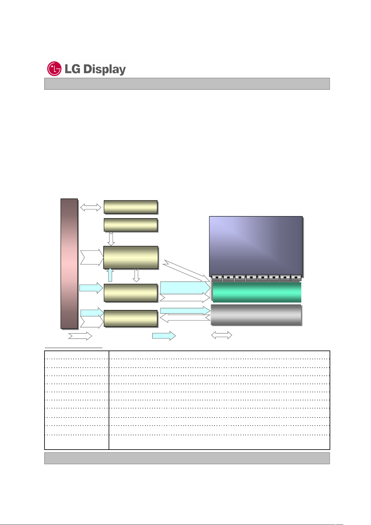
1. General Description
General Features
Anti-Glare treatment of the front polarizerSurface Treatment
6-bit, 262,144 colorsColor Depth
1366 horiz. By 768 vert. Pixels RGB strip arrangementPixel Format
200 cd/m2(Typ.5 point)Luminance, White
Total 4.1 Watt(Typ.) @ LCM circuit 1.3 Watt(Typ.), B/L input 2.8Watt(Typ. with Driver)Power Consumption
350g (Max.)Weight
Transmissive mode, normally whiteDisplay Operating Mode
Yes
RoHS & Halogen Free C
omply
0.2265mm × 0.2265 mmPixel Pitch
323.5(H, typ) × 192.0(V, typ) × 5.2(D,max) [mm]Outline Dimension
14.0 inches diagonal Active Screen Size
The LP140WH1 is a Color Active Matrix Liquid Crystal Display with an integral LED backlight system. The
matrix employs a-Si Thin Film Transistor as the active element. It is a transmissive type display operating in
the normally white mode. This TFT-LCD has 14.0 inches diagonally measured active display area with HD r
esolution(768 vertical by 1366 horizontal pixel array). Each pixel is divided into Red, Green and Blue sub-pix
els or dots which are arranged in vertical stripes. Gray scale or the brightness of the sub-pixel color is deter
mined with a 6-bit gray scale signal for each dot, thus, presenting a palette of more than 262,144 colors.
The LP140WH1 has been designed to apply the interface method that enables low power, high speed, low
EMI.
The LP140WH1 is intended to support applications where thin thickness, low power are critical factors and
graphic displays are important. In combination with the vertical arrangement of the sub-pixels, the LP140W
H1 characteristics provide an excellent flat display for office automation products such as Notebook PC.
Control & Data Power EDID signal & Power
TFT-LCD Panel
(HD, GIP, TN)
1
Timing Control
(Tcon) Block
Timing Control
(Tcon) Block
User connector 40 Pin
EEPROM Block
for EDID
EEPROM Block
for EDID
Source Driver
(Bottom Bent)
LED Backlight Ass’y
TCLKs
LVDS
1port
VCC
LED Driver
Block
LED Driver
Block
FB1~6
EEPROM Block
for Tcon Operating
EEPROM Block
for Tcon Operating
Power
Block
Power
Block
AVCC, AVDD
VGH, VGL, GMA
Mini-LVDS
GIP CLKs, DSC
VOUT_LED
DVCC
VLED
LED_EN
PWM
768
1366
Page 5
Product Specification
5 / 27
LP140WH1
Liquid Crystal Display
Ver. 1.0 Oct.09, 2009
2. Absolute Maximum Ratings
The following are maximum values which, if exceeded, may cause faulty operation or damage to the unit.
Table 1. ABSOLUTE MAXIMUM RATINGS
Storage
Operation
10
20 30 40 50
60 70 800
-20
Dry Bulb Temperature [℃]
10%
20%
40%
60%
90% 80%
0
10
20
30
40
50
60
Wet Bulb
Temperature [℃]
Humidity[(%)RH]
Units
1%RH9010HOP
Operating Ambient Humidity
1%RH9010HST
Storage Humidity
1C60-20HST
Storage Temperature
1C500TOP
Operating Temperature
at 25 5CVdc4.0-0.3VCC
Power Input Voltage
MaxMin
Parameter Notes
Values
Symbol
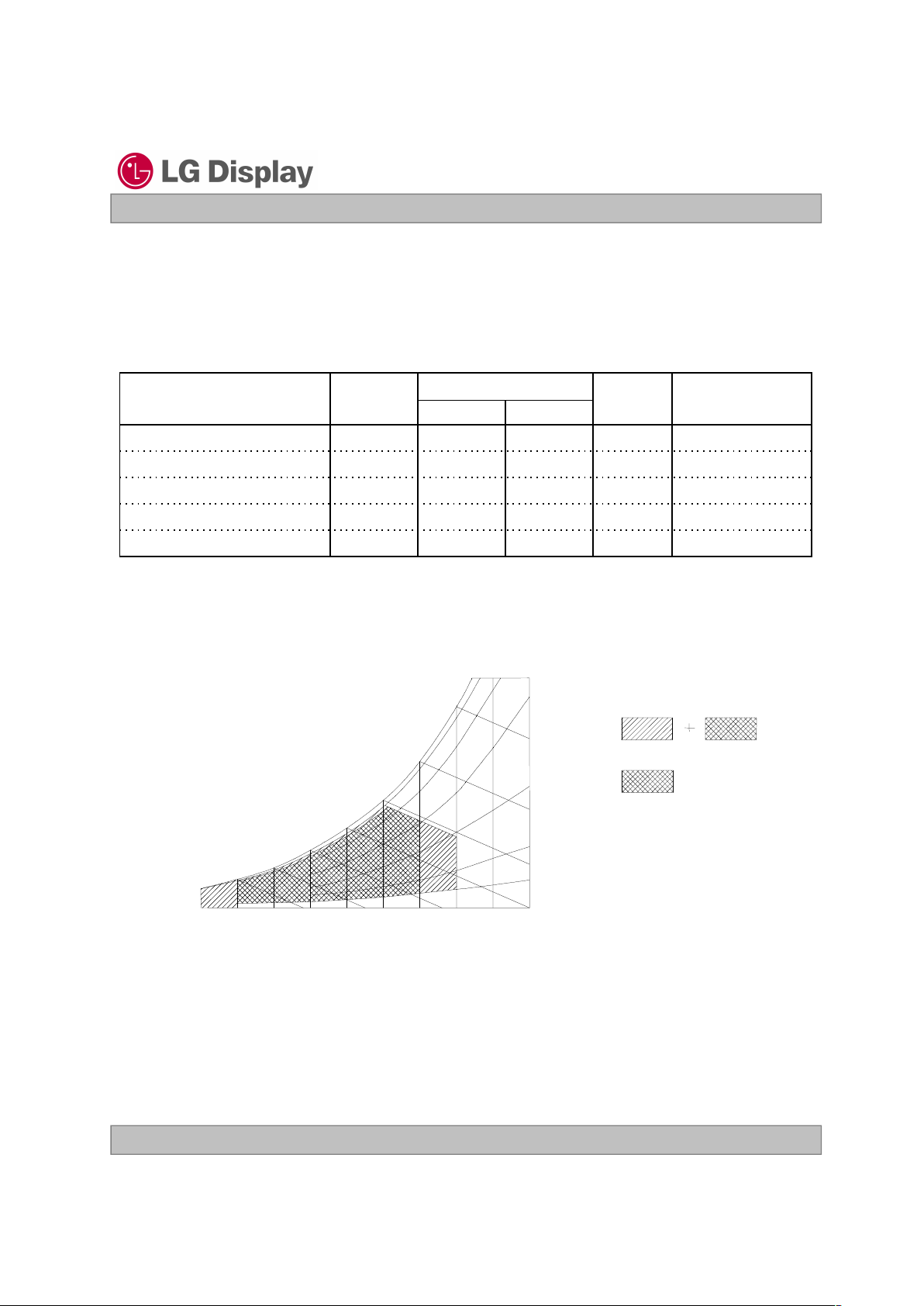
Note : 1. Temperature and relative humidity range are shown in the figure below.
Wet bulb temperature should be 39C Max, and no condensation of water.
Page 6
Product Specification
6 / 27
LP140WH1
Liquid Crystal Display
Ver. 1.0 Oct.09, 2009
Table 2. ELECTRICAL CHARACTERISTICS
3. Electrical Specifications
3-1. Electrical Characteristics
The LP140WH1 requires two power inputs. The first logic is employed to power the LCD electronics and to
drive the TFT array and liquid crystal. The second backlight is the input about LED BL.with LED Driver.
12Hrs--12,000 Life Time
V0.5-0
VLED_EN
_L
LED_EN Low Voltage
V5.3-3.0
VLED_EN
_H
LED_EN High Voltage
kΩ604020ZPWM LED_EN Impedance
V0.5-0
V
PWM_L
PWM Low Level Voltage
V
5.3-3.0
V
PWM_H
PWM High Level Voltage
11
Hz
1000-200
FPWM
PWM Frequency
kΩ604020ZPWM PWM Impedance
10%0.3-0
-
PWM Jitter
9
%
100-6 PWM Duty Ratio
7W3.02.8-PLED LED Power Consumption
7mA255230- ILED LED Power Input Current
6V20.012.07.0VLED LED Power Input Voltage
BACKLIGHT : ( with LED Driver)
5
Ω
11010090ZLVDS LVDS Impedance
4mA1500--ICC_P Power Supply Inrush Current
2W1.51.3-PCC Power Consumption
3mA595500-ICC_max
Black
2mA470400-ICC
Mosaic
Power Supply Input Current
1V3.63.33.0VCC Power Supply Input Voltage
LOGIC :
MaxTypMin
NotesUnit
Values
SymbolParameter
Page 7
Product Specification
7 / 27
LP140WH1
Liquid Crystal Display
Ver. 1.0 Oct.09, 2009
Note)
1. The measuring position is the connector of LCM and the test conditions are under 25℃, fv = 60Hz,
Black pattern.
2. The specified Icc current and power consumption are under
the Vcc = 3.3V , 25℃, fv = 60Hz condition whereas Mosaic pattern
is displayed and fv is the frame frequency.
3. This Spec. is the max load condition for the cable impedance designing.
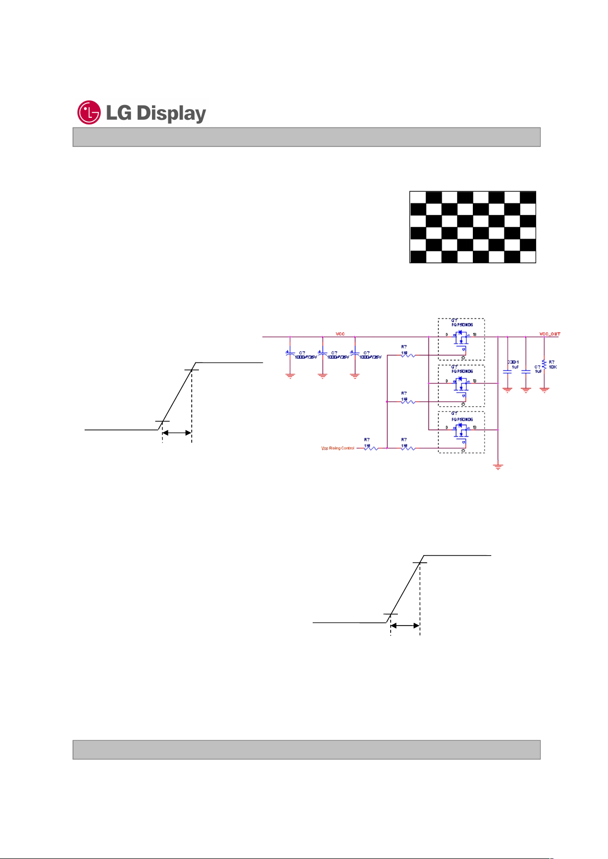
4. The below figures are the measuring Vcc condition and the Vcc control block LGD used.
The Vcc condition is same the minimum of T1 at Power on sequence.
5. This impedance value is needed to proper display and measured form LVDS Tx to the mating connector.
6. The measuring position is the connector of LCM and the test conditions are under 25℃.
7. The current and power consumption with LED Driver are under the Vled = 12.0V , 25℃, Dimming of
Max luminance whereas White pattern is displayed and fv is the frame frequency.
8. The below figures are the measuring Vled condition
and the Vled control block LGD used.
VLED control block is same with Vcc control block.
9. The operation of LED Driver below minimum dimming ratio may cause flickering or reliability issue.
10. If Jitter of PWM is bigger than maximum. It may cause flickering.
11. This Spec. is not effective at 100% dimming ratio as an exception because it has DC level equivalent
to 0Hz. In spite of acceptable range as defined, the PWM Frequency should be fixed and stable for
more consistent brightness control at any specific level desired.
12 The life time is determined as the time at which the typical brightness of LCD is 50% compare to that of
initial value at the typical LED current. These LED backlight has 6 strings on it and the typical current
of LED’s string is base on 18mA.
10%
90%
0.5ms
3.3V
0V
10%
90%
0.5ms
12.0V
0V
Rising time
Vcc
Rising time
VLED
Page 8
Product Specification
8 / 27
LP140WH1
Liquid Crystal Display
Ver. 1.0 Oct.09, 2009
3-2. Interface Connections
Table 3. MODULE CONNECTOR PIN CONFIGURATION (CN1)
LED Power Supply 7V-21V VLED
40
LED Power Supply 7V-21V VLED
39
LED Power Supply 7V-21V VLED
38
No Connection (Reserved)NC
37
Backlight On/Off ControlLED_EN
36
PWM for luminance controlPWM
35
No ConnectionNC
34
LED GroundVLED_GND
33
LED GroundVLED_GND
32
LED GroundVLED_GND
31
No ConnectionNC20
GroundGND19
Positive LVDS differential clock inputOdd_CLKIN+18
Negative LVDS differential clock inputOdd_CLKIN-17
GroundGND16
Positive LVDS differential data input
Odd_RIN 2+
15
Negative LVDS differential data input
Odd_RIN 2-
14
GroundGND13
Positive LVDS differential data input
Odd_RIN 1+
12
Negative LVDS differential data input
Odd_RIN 1-
11
No ConnectionNC30
Power Supply, 3.3V Typ.VCC2
Power Supply, 3.3V Typ.VCC3
DDC 3.3V powerV EEDID4
No ConnectionNC5
DDC ClockClk EEDID6
DDC DataDATA EEDID7
Positive LVDS differential data input
Odd_RIN 0+
9
No ConnectionNC1
Negative LVDS differential data input
Odd_RIN 0-
8
GroundGND10
GroundGND19
No ConnectionNC23
No ConnectionNC24
GroundGND19
No ConnectionNC26
No ConnectionNC27
GroundGND19
No ConnectionNC29
NotesDescriptionSymbolPin
NC No Connection21
1, Interface chips
1.1 LCD : SW, SW0624 (LCD Controller)
including LVDS Receiver
1.2 System : THC63LVDF823A
or equivalent
* Pin to Pin compatible with LVDS
2. Connector
2.1 LCD : CABLINE-VS RECE ASS’Y, I-PEX
or its compatibles
2.2 Mating : CABLINE-VS PLUG CABLE
ASS’Y or equivalent.
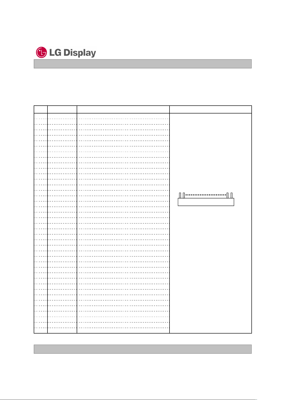
2.3 Connector pin arrangement
1
40
[LCD Module Rear View]
This LCD employs two interface connections, a 40 pin connector is used for the module electronics interface an
d the other connector is used for the integral backlight system.
The electronics interface connector is a model CABLINE-VS RECE ASS’Y manufactured by I-PEX.
Page 9
Product Specification
9 / 27
LP140WH1
Liquid Crystal Display
Ver. 1.0 Oct.09, 2009
NotesUnitMaxMinSymbolDescription
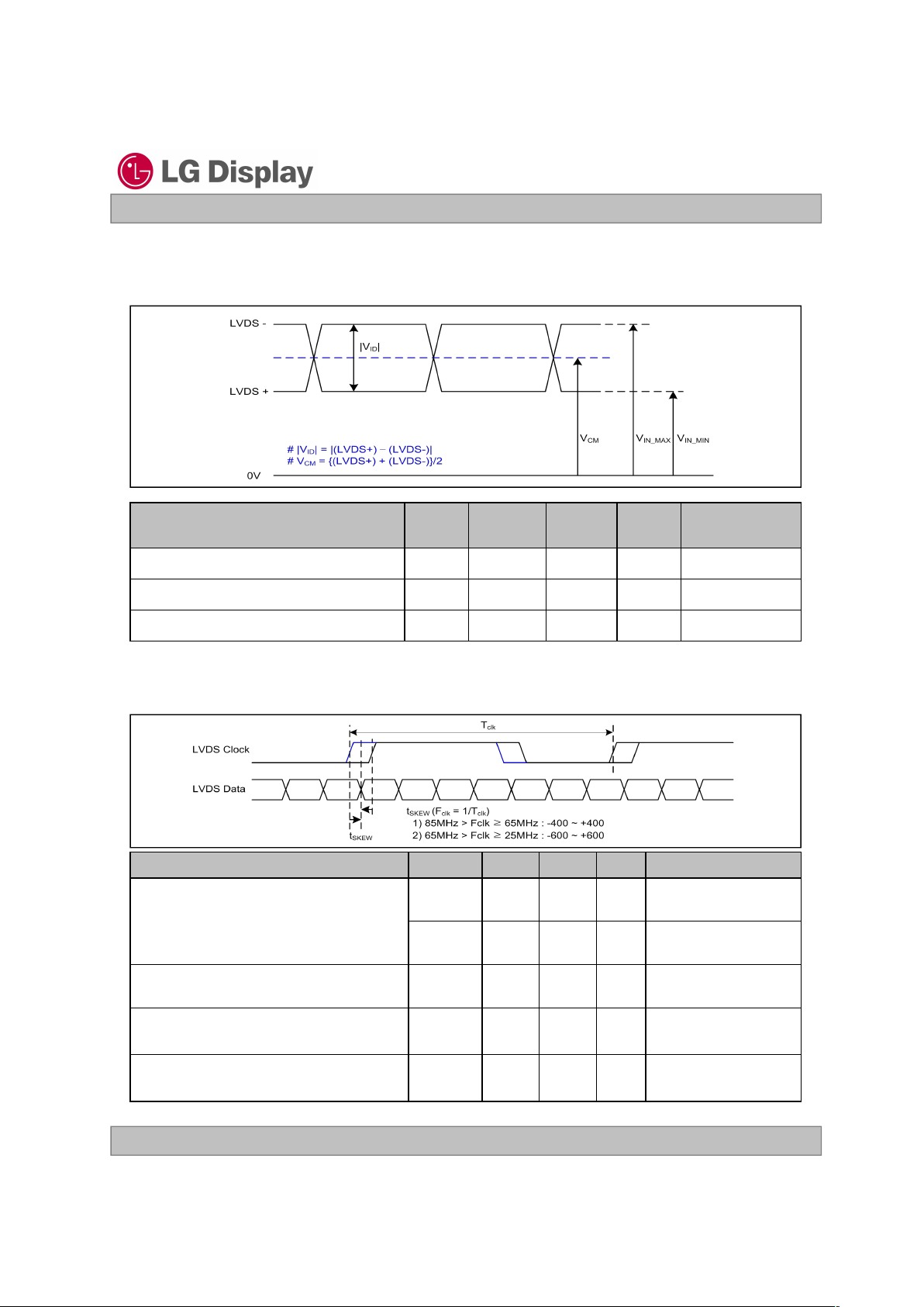
85MHz > Fclk ≥ 65M
Hz
ps
+ 400- 400
t
SKEW
LVDS Clock to Data Skew Margin
-
-
-
65MHz > Fclk ≥ 25M
Hz
%± 3-
F
DEV
Maximum deviation
of input clock frequency during SSC
KHz200-
F
MOD
Maximum modulation frequency
of input clock during SSC
- 1/7
- 600
T
clk
+ 1/7
t
SKEW_EO
LVDS Clock to Clock Skew Margin (Even
to Odd)
ps
+ 600
t
SKEW
-V2.10.3
V
IN
LVDS Input Voltage Range
-V1.80.6
V
CM
LVDS Common mode Voltage
-mV600100
|VID|
LVDS Differential Voltage
NotesUnitMaxMin
Symb
ol
Description
3-3-1. DC Specification
3-3-2. AC Specification
3-3. LVDS Signal Timing Specifications
Page 10

Product Specification
10 / 27
LP140WH1
Liquid Crystal Display
Ver. 1.0 Oct.09, 2009
< Clock skew margin between channel >
< LVDS Data Format >
3-3-3. Data Format
1) LVDS 1 Port
< Spread Spectrum >
Time
F
center
F
max
F
min
F
MOD
1
F
center
* F
DEV
Freq.
G0 R5 R4 R3 R2 R1 R0
B1 B0 G5 G4 G3 G2 G1
DE VSYNC HSYNC B5 B4 B3 B2
X B7 B6 G7 G6 R7 R6
R1 R0
G2 G1
B3 B2
R7 R6
G0
B1
DE
X
Current (Nth ) Cycle
R5 R4
B0 G5
VSYNC HSYNC
B7 B6
R3 R2
G4 G3
B5 B4
G7 G6
Previous (N-1)th Cycle Next (N+1) th Cycle
RCLK+
RA+/-
RB+/-
RC+/-
RD+/-
Page 11

Product Specification
11 / 27
LP140WH1
Liquid Crystal Display
Ver. 1.0 Oct.09, 2009
3-4. Signal Timing Specifications
Table 4. TIMING TABLE
This is the signal timing required at the input of the User connector. All of the interface signal timing should be
satisfied with the following specifications and specifications of LVDS Tx/Rx for its proper operation.
3-5. Signal Timing Waveforms
Condition : VCC =3.3V
Low: 0.3VCC
High: 0.7VCC
Data Enable, Hsync, Vsync
Hsync
Data Enable
Vsync
Data Enable
t
WH
t
HP
t
HFP
t
HBP
t
VP
t
WV
t
VBP
t
VFP
tWHA
tWVA
tCLK
0.5 Vcc
DCLK
768768768
t
WVA
Width-Active
136613661366
t
WHA
Width-Active
tCLK
724824
t
HBP
Horizontal back porch
56328
t
HFP
Horizontal front porch
tHP
18138
t
VBP
Vertical back porch
531
t
VFP
Vertical front porch
tHP
800790780
tVP
Period
963
tWV
Width
24168
tWH
Width
tCLK
151814621406
t
HP
Period
Hsync
Vsync
Data
Enable
MHz-69.3-
f
CLK
FrequencyDCLK
Not eUn itM a xTypMinSym bolI TEM
Page 12

Product Specification
12 / 27
LP140WH1
Liquid Crystal Display
Ver. 1.0 Oct.09, 2009
3-6. Color Input Data Reference
The brightness of each primary color (red,green and blue) is based on the 6-bit gray scale data input for the
color ; the higher the binary input, the brighter the color. The table below provides a reference for color
versus data input.
Table 5. COLOR DATA REFERENCE
0 0 0 0 0 00 0 0 0 0 00 0 0 0 0 0
GREEN (00)
GREEN
0 0 0 0 0 00 0 0 0 0 10 0 0 0 0 0
GREEN (01)
………
...
0 0 0 0 0 01 1 1 1 1 00 0 0 0 0 0
GREEN (62)
0 0 0 0 0 01 1 1 1 1 10 0 0 0 0 0
GREEN (63)
0 0 0 0 0 00 0 0 0 0 00 0 0 0 0 0
RED (00)
RED
0 0 0 0 0 00 0 0 0 0 00 0 0 0 0 1
RED (01)
………
…
0 0 0 0 0 00 0 0 0 0 01 1 1 1 1 0
RED (62)
0 0 0 0 0 00 0 0 0 0 01 1 1 1 1 1
RED (63)
0 0 0 0 0 10 0 0 0 0 00 0 0 0 0 0
BLUE (01)
………
…
1 1 1 1 1 00 0 0 0 0 00 0 0 0 0 0
BLUE (62)
1 1 1 1 1 10 0 0 0 0 00 0 0 0 0 0
BLUE (63)
BLUE (00)
White
Yellow
Magenta
Cyan
Blue
Green
Red
Black
0 0 0 0 0 00 0 0 0 0 00 0 0 0 0 0
Basic
Color
0 0 0 0 0 00 0 0 0 0 01 1 1 1 1 1
0 0 0 0 0 01 1 1 1 1 10 0 0 0 0 0
1 1 1 1 1 10 0 0 0 0 00 0 0 0 0 0
1 1 1 1 1 11 1 1 1 1 10 0 0 0 0 0
1 1 1 1 1 10 0 0 0 0 01 1 1 1 1 1
0 0 0 0 0 01 1 1 1 1 11 1 1 1 1 1
1 1 1 1 1 11 1 1 1 1 11 1 1 1 1 1
BLUE
M S B L S B
GREEN
M S B L S B
RED
M S B L S B
B 5 B 4 B 3 B 2 B 1 B 0G 5 G 4 G 3 G 2 G 1 G 0R 5 R 4 R 3 R 2 R 1 R 0
0 0 0 0 0 00 0 0 0 0 00 0 0 0 0 0
BLUE
Color
Input Color Data
Page 13

Product Specification
13 / 27
LP140WH1
Liquid Crystal Display
Ver. 1.0 Oct.09, 2009
Note)
1. Do not insert the mating cable when system turn on.
2. Valid Data have to meet “3-3. LVDS Signal Timing Specifications”
3. LVDS, LED_EN and PWM need to pull-down condition on invalid status.
4. LGD recommend the rising sequence of VLED after the Vcc and valid status of LVDS turn on.
Table 6. POWER SEQUENCE TABLE
ms--0.5T
12
ms--10T
11
ms--0T
10
ms--0T
9
ms--10T
8
Max.Typ.Min.
Units
Value
LED
Parameter
3-7. Power Sequence
ms--200T
5
ms--400T
4
ms10-3T
7
ms--200T
6
ms50-0T
3
ms50-0T
2
ms10-0.5T
1
Max.Typ.Min.
Units
Value
Logic
Parameter
T
7
Interface Signal, V
i
LVDS
Power Supply Input
VCC
90%
10%10%
0V
90%
T
1
T
2
T
3
T
4
T
5
T
6
0V
Dimming control signal
Of LED BL
PWM
0V (Low)
T
8
LED input Voltage
VLED
T
10
LED on/off control Signal
LED_EN
T
11
T
9
Valid Data
0V
Valid Data
0V (Off)
90%
10%
T
12
90%
Page 14

Product Specification
14 / 27
LP140WH1
Liquid Crystal Display
Ver. 1.0 Oct.09, 2009
4. Optical Specification
FIG. 1 Optical Characteristic Measurement Equipment and Method
Table 7. OPTICAL CHARACTERISTICS
Ta=25C, VCC=3.3V, fV=60Hz, f
CLK
= 72.3MHz, I
LED
= 18 mA
5Viewing Angle
Color Coordinates
4ms-16-
TrR+ Tr
D
Response Time
0.1480.1180.088
BY
0.343 0.313 0.283
WXWHITE
y axis, down (=270)
y axis, up (=90)
x axis, left (=180)
x axis, right(=0) degree--40r
degree--40l
degree--10u
degree--30d
BLUE
0.3590.329 0.299
WY
6Gray Scale
GREEN
RED
0.3680.3380.308
GX
0.5800.5500.520
GY
0.6210.5910.561
RX
0.3800.3500.320
RY
31.61.4-
WHITE
Luminance Variation
0.1860.1560.126
BX
MaxTypMin
1--300CRContrast Ratio
2cd/m
2
-200170
L
WH
Surface Luminance, white
Parameter Symbol NotesUnits
Values
LCD Module
Optical Stage(x,y)
Pritchard 880 or
equivalent
50cm
Optical characteristics are determined after the unit has been ‘ON’ and stable for approximately 30 minutes in
a dark environment at 25C. The values specified are at an approximate distance 50cm from the LCD surface
at a viewing angle of and equal to 0.
FIG. 1 presents additional information concerning the measurement equipment and method.
Page 15

Product Specification
15 / 27
LP140WH1
Liquid Crystal Display
Ver. 1.0 Oct.09, 2009
100L63
79.40L55
10.59L23
19.92L31
34.80L39
55.61L47
4.30L15
0.97L7
0.16L0
Luminance [%] (Typ)Gray Level
Note)
1. Contrast Ratio(CR) is defined mathematically as
Surface Luminance with all white pixels
Contrast Ratio =
Surface Luminance with all black pixels
2. Surface luminance is the average of 5 point across the LCD surface 50cm from the surface with
all pixels displaying white. For more information see FIG 1.
LWH = Average(L1,L2, … L5)
3. The variation in surface luminance , The panel total variation (
WHITE
) is determined by measuring L
N
at each test position 1 through 13 and then defined as followed numerical formula.
For more information see FIG 2.
Maximum(L1,L2, … L13)
WHITE
=
Minimum(L1,L2, … L13)
4. Response time is the time required for the display to transition from white to black (rise time, TrR) and
from black to white(Decay Time, TrD). For additional information see FIG 3.
5. Viewing angle is the angle at which the contrast ratio is greater than 10. The angles are determined
for the horizontal or x axis and the vertical or y axis with respect to the z axis which is normal to the
LCD surface. For more information see FIG 4.
6. Gray scale specification * fV = 60Hz
Page 16

Product Specification
16 / 27
LP140WH1
Liquid Crystal Display
Ver. 1.0 Oct.09, 2009
FIG. 3 Response Time
The response time is defined as the following figure and shall be measured by switching the input signal
for “black” and “white”.
Tr
R
Tr
D
100
90
10
0
%
Optical
Response
white
black
white
FIG. 2 Luminance
<measuring point for surface luminance & measuring point for luminance variation>
H
A
V
B
L4 L5
L1
L2
L3
Center Point
D
C
H,V : ACTIVE AREA
A : H/4 mm
B : V/4 mm
C : 10 mm
D : 10 mm
POINTS : 13 POINTS
L12
L7
L9
L10
L6
L11 L13
L8
Page 17

Product Specification
17 / 27
LP140WH1
Liquid Crystal Display
Ver. 1.0 Oct.09, 2009
5. Mechanical Characteristics
The contents provide general mechanical characteristics for the model LP140WH1. In addition the figures
in the next page are detailed mechanical drawing of the LCD.
173.95 mmVertical
Anti-Glare treatment of the front polarizer
Surface Treatment
350g (Max.)Weight
177.4 0.5mmVertical
192.0 0.5mmVertical
5.2mm (max)Thickness
309.40 mmHorizontal
Active Display Area
314.4 0.5mmHorizontal
Bezel Area
323.5 0.5mmHorizontal
Outline Dimension
Page 18

Product Specification
18 / 27
LP140WH1
Liquid Crystal Display
Ver. 1.0 Oct.09, 2009
<FRONT VIEW>
Note) Unit:[mm], General tolerance: 0.5mm
Page 19

Product Specification
19 / 27
LP140WH1
Liquid Crystal Display
Ver. 1.0 Oct.09, 2009
<REAR VIEW>
Note) Unit:[mm], General tolerance: 0.5mm
Page 20

Product Specification
20 / 27
LP140WH1
Liquid Crystal Display
Ver. 1.0 Oct.09, 2009
[ DETAIL DESCRIPTION OF SIDE MOUNTING SCREW ]
Notes : 1. Screw plated through the method of non-electrolytic nickel plating is preferred
to reduce possibility that results in vertical and/or horizontal line defect due to
the conductive particles from screw surface.
* Mounting Screw Length (A)
= 2.0(Min) / 2.5(Max)
* Mounting Screw Hole Depth (B)
= 2.5(Min)
* Mounting hole location : 3.1(typ.)
* Torque : 2.0 kgf.cm(Max)
(Measurement gauge : torque meter)
Page 21

Product Specification
21 / 27
LP140WH1
Liquid Crystal Display
Ver. 1.0 Oct.09, 2009
6. Reliability
Environment test condition
{ Result Evaluation Criteria }
There should be no change which might affect the practical display function when the display quality
test is conducted under normal operating condition.
0 ~ 10,000 feet (3,048m) 24Hr
0 ~ 40,000 feet (12,192m) 24Hr
Altitude operating
storage / shipment
7
Half sine wave, 180G, 2ms
one shock of each six faces(I.e. run 180G 2ms
for all six faces)
Shock test (non-operating)6
Sine wave, 10 ~ 500 ~ 10Hz, 1.5G, 0.37oct/min
3 axis, 1hour/axis
Vibration test (non-operating)5
Ta= 0C, 240hLow temperature operation test4
Ta= 50C, 50%RH, 240hHigh temperature operation test3
Ta= -20C, 240hLow temperature storage test2
Ta= 60C, 240hHigh temperature storage test1
ConditionsTest ItemNo.
Page 22

Product Specification
22 / 27
LP140WH1
Liquid Crystal Display
Ver. 1.0 Oct.09, 2009
7. International Standards
7-1. Safety
7-2. EMC
a) ANSI C63.4 “Methods of Measurement of Radio-Noise Emissions from Low-Voltage Electrical and
Electrical Equipment in the Range of 9kHZ to 40GHz. “American National Standards Institute(ANSI),
1992
b) C.I.S.P.R “Limits and Methods of Measurement of Radio Interface Characteristics of Information
Technology Equipment.“ International Special Committee on Radio Interference.
c) EN 55022 “Limits and Methods of Measurement of Radio Interface Characteristics of Information
Technology Equipment.“ European Committee for Electrotechnical Standardization.(CENELEC), 1998
( Including A1: 2000 )
a) UL 60950-1:2003, First Edition, Underwriters Laboratories, Inc.,
Standard for Safety of Information Technology Equipment.
b) CAN/CSA C22.2, No. 60950-1-03 1st Ed. April 1, 2003, Canadian Standards Association,
Standard for Safety of Information Technology Equipment.
c) EN 60950-1:2001, First Edition,
European Committee for Electrotechnical Standardization(CENELEC)
European Standard for Safety of Information Technology Equipment.
Page 23

Product Specification
23 / 27
LP140WH1
Liquid Crystal Display
Ver. 1.0 Oct.09, 2009
8. Packing
8-2. Packing Form
8-1. Designation of Lot Mark
a) Lot Mark
A B C D E F G H I J K L M
A,B,C : SIZE(INCH) D : YEAR
E : MONTH F ~ M : SERIAL NO.
Note
1. YEAR
2. MONTH
Mark
Year
0
2010
6
2006720078200892009
4
200452005
321
200320022001
B
Nov
Mark
Month
A
Oct
6
Jun7Jul8Aug9Sep
4
Apr5May
C321
DecMarFebJan
b) Location of Lot Mark
Serial No. is printed on the label. The label is attached to the backside of the LCD module.
This is subject to change without prior notice.
a) Package quantity in one box : 30 pcs
b) Box Size : 490 mm × 390 mm × 256 mm
Page 24

Product Specification
24 / 27
LP140WH1
Liquid Crystal Display
Ver. 1.0 Oct.09, 2009
9. PRECAUTIONS
Please pay attention to the followings when you use this TFT LCD module.
9-1. MOUNTING PRECAUTIONS
(1) You must mount a module using holes arranged in four corners or four sides.
(2) You should consider the mounting structure so that uneven force (ex. Twisted stress) is not applied to the
module. And the case on which a module is mounted should have sufficient strength so that external
force is not transmitted directly to the module.
(3) Please attach the surface transparent protective plate to the surface in order to protect the polarizer.
Transparent protective plate should have sufficient strength in order to the resist external force.
(4) You should adopt radiation structure to satisfy the temperature specification.
(5) Acetic acid type and chlorine type materials for the cover case are not desirable because the former
generates corrosive gas of attacking the polarizer at high temperature and the latter causes circuit break
by electro-chemical reaction.
(6) Do not touch, push or rub the exposed polarizers with glass, tweezers or anything harder than HB
pencil lead. And please do not rub with dust clothes with chemical treatment.
Do not touch the surface of polarizer for bare hand or greasy cloth.(Some cosmetics are detrimental
to the polarizer.)
(7) When the surface becomes dusty, please wipe gently with absorbent cotton or other soft materials like
chamois soaks with petroleum benzene. Normal-hexane is recommended for cleaning the adhesives
used to attach front / rear polarizers. Do not use acetone, toluene and alcohol because they cause
chemical damage to the polarizer.
(8) Wipe off saliva or water drops as soon as possible. Their long time contact with polarizer causes
deformations and color fading.
(9) Do not open the case because inside circuits do not have sufficient strength.
9-2. OPERATING PRECAUTIONS
(1) The spike noise causes the mis-operation of circuits. It should be lower than following voltage :
V=± 200mV(Over and under shoot voltage)
(2) Response time depends on the temperature.(In lower temperature, it becomes longer.)
(3) Brightness depends on the temperature. (In lower temperature, it becomes lower.)
And in lower temperature, response time(required time that brightness is stable after turned on) becomes
longer.
(4) Be careful for condensation at sudden temperature change. Condensation makes damage to polarizer or
electrical contacted parts. And after fading condensation, smear or spot will occur.
(5) When fixed patterns are displayed for a long time, remnant image is likely to occur.
(6) Module has high frequency circuits. Sufficient suppression to the electromagnetic interference shall be
done by system manufacturers. Grounding and shielding methods may be important to minimized the
interference.
Page 25

Product Specification
25 / 27
LP140WH1
Liquid Crystal Display
Ver. 1.0 Oct.09, 2009
Since a module is composed of electronic circuits, it is not strong to electrostatic discharge. Make certain that
treatment persons are connected to ground through wrist band etc. And don’t touch interface pin directly.
9-3. ELECTROSTATIC DISCHARGE CONTROL
Strong light exposure causes degradation of polarizer and color filter.
9-4. PRECAUTIONS FOR STRONG LIGHT EXPOSURE
9-5. STORAGE
(1) When the protection film is peeled off, static electricity is generated between the film and polarizer.
This should be peeled off slowly and carefully by people who are electrically grounded and with well
ion-blown equipment or in such a condition, etc.
(2) The protection film is attached to the polarizer with a small amount of glue. If some stress is applied
to rub the protection film against the polarizer during the time you peel off the film, the glue is apt to
remain on the polarizer.
Please carefully peel off the protection film without rubbing it against the polarizer.
(3) When the module with protection film attached is stored for a long time, sometimes there remains a
very small amount of glue still on the polarizer after the protection film is peeled off.
(4) You can remove the glue easily. When the glue remains on the polarizer surface or its vestige is
recognized, please wipe them off with absorbent cotton waste or other soft material like chamois
soaked with normal-hexane.
9-6. HANDLING PRECAUTIONS FOR PROTECTION FILM
When storing modules as spares for a long time, the following precautions are necessary.
(1) Store them i n a dark place. Do not expose the module to sunli gh t or fluorescent light . Keep the
temperature between 5C and 35C at normal humidity.
(2) The polarizer surface should not come in contact with any other object.
It is recommended that they be stored in the container in which they were shipped.
Page 26

Product Specification
26 / 27
LP140WH1
Liquid Crystal Display
Ver. 1.0 Oct.09, 2009
APPENDIX A. Enhanced Extended Display Identification Data (EEDIDTM) 1/3
Page 27

Product Specification
27 / 27
LP140WH1
Liquid Crystal Display
Ver. 1.0 Oct.09, 2009
APPENDIX A. Enhanced Extended Display Identification Data (EEDIDTM) 2/3
Page 28

Product Specification
28 / 27
LP140WH1
Liquid Crystal Display
Ver. 1.0 Oct.09, 2009
APPENDIX A. Enhanced Extended Display Identification Data (EEDIDTM) 3/3
 Loading...