

Page 1
()Preliminary Specification
◆
()Final Specification
Title 14.0”W HD+ TFT LCD
LP140WD1
Liquid Crystal Display
Product Specification
SPECIFICATION
FOR
APPROVAL
Customer HP
MODEL
SIGNATUREAPPROVED BY
/
/
/
SUPPLIER LG Display Co., Ltd.
*MODEL LP140WD1
Suffix TLD2
*When you obtain standard approval,
please use the above model name without suffix
APPROVED BY
APPROVED BY
G. J. Kwon / S.Manager
REVIEWED BY
REVIEWED BY
S. R. Kim / Manager
PREPARED BY
PREPARED BY
D. G. Choi / Engineer
SIGNATURE
SIGNATURE
Please return 1 copy for your confirmation with
your signature and comments.
Ver. 1.0 Dec. 15. 2009
Products Engineering Dept.
LG Display Co., Ltd
1/ 31
Page 2
Product Specification
Contents
LP140WD1
Liquid Crystal Display
No ITEM
COVER
CONTENTS
RECORD OF REVISIONS
1 GENERAL DESCRIPTION
2 ABSOLUTE MAXIMUM RATINGS
3 ELECTRICAL SPECIFICATIONS
3-1 ELECTRICAL CHARACTREISTICS
3-2 INTERFACE CONNECTIONS
3-3 LVDS SIGNAL TIMING SPECIFICATION
3-4 SIGNAL TIMING SPECIFICATIONS
3-5 SIGNAL TIMING WAVEFORMS
3-6 COLOR INPUT DATA REFERNECE
3-7 POWER SEQUENCE
4 OPTICAL SFECIFICATIONS
Page
1
2
3
4
5
6-7
8
9-10
11
11
12
13
14-16
5 MECHANICAL CHARACTERISTICS
6 RELIABLITY
7 INTERNATIONAL STANDARDS
7-1 SAFETY
7-2 EMC
7-3 Environment
8 PACKING
8-1 DESIGNATION OF LOT MARK
8-2 PACKING FORM
9 PRECAUTIONS
A APPENDIX. Enhanced Extended Display Identification Data
Ver. 1.0 Dec. 15. 2009
17-23
24
25
25
25
26
26
27-28
29-31
2/ 31
Page 3
Product Specification
RECORD OF REVISIONS
LP140WD1
Liquid Crystal Display
Revision No Revision Date Page Description
0.0 Jul. 07, 2009 All First Draft (Preliminary Specification) 0.0
0.1 Dec.11.2009 14,15 update optical Specification
EDID
ver
1.0Final Specification-Dec.15. 20091.0
Ver. 1.0 Dec. 15. 2009
3/ 31
Page 4
LP140WD1
Liquid Crystal Display
Product Specification
1. General Description
The LP140WD1 is a Color Active Matrix Liquid Crys tal Display with an integra l LED backlight system. The
matrix employs a-Si Thin Film Tran s istor as the active element. It is a trans missi ve type d isplay operating in
the normally white mode. This TFT-LCD has 14.0 inches diagonally measured active display area with HD
resolution(900 vertical by 1600 horizontal pixel a rray). Each pixel is divided into Red, Green and Blue subpixels or dots which are arranged in vertical stripes. Gray scale or the brightness o f the sub-pixel color is
determined with a 6-bit gray scale signal for each dot, thus, presenting a palette of more than 262,144
colors.
The LP140WD1 has been designed to apply the in terface method that enables low power, high speed, low
EMI.
The LP140WD1 is intended to support applications where thin th ickness, low power are critical factor s and
graphic displays are important. In combination with the vertical arrangement of the sub-pixels, the
LP140WD1 characteristics provide an exce llen t fla t display for office automation products such as Notebook
PC.
Block
CN2
CN2
9Pin
9Pin
FPC
FPC
1
GIP(Gate In Panel)
WLED Ass’y(48ea)
TFT-LCD Panel
(1600 X 900)
900
1
Source Driver Circuit
Source Driver Circuit
Power EDID signal & Power
LED
CN 1 User connector 40 Pin
LED
Driver
Driver
EDID
EDID
BLOCK
BLOCK
POWER
POWER
BLOCK
BLOCK
EEPROM
EEPROM
BLOCK
BLOCK
LVDS & Timing
LVDS & Timing
Control
Control
Block
Control & Data
General Features
Active Screen Size 14.0 inches diagonal
Outline Dimension 323.5(H, typ) × 192.0(V, typ) × 5.2(D,max) [mm]
Pixel Pitch 0.1935mm × 0.1935 mm
Pixel Format 1600 horiz. By 900 vert. Pixels RGB strip arrangement
Color Depth 6-bit, 262,144 colors
2
Luminance, White 200 cd/m
Power Consumption Total 5.0 Watt (Typ.) @ Logic input 1.45 Watt (Typ.), B/L input 3.56 Watt (Typ.)
Weight 375g (Max.)
Display Operating Mode Transmissive mode, normally white
Surface Treatment Anti-glare treatment of the front polarizer
RoHS Comply Yes
(Typ.5 point)
1600
Ver. 1.0 Dec. 15. 2009
4/ 31
Page 5
LP140WD1
Liquid Crystal Display
Product Specification
2. Absolute Maximum Ratings
The following are maximum values which, if exceeded, may cause faulty operation or damage to the unit.
Table 1. ABSOLUTE MAXIMUM RATINGS
Parameter Symbol
Power Input Voltage
Operating Temperature
Storage Temperature
Operating Ambient Humidity
Storage Humidity
VCC -0.3 4.0 Vdc at 25 5C
TOP 050C1
HST -20 60 C1
HOP 10 90 %RH 1
HST 10 90 %RH 1
Values
Units Notes
Min Max
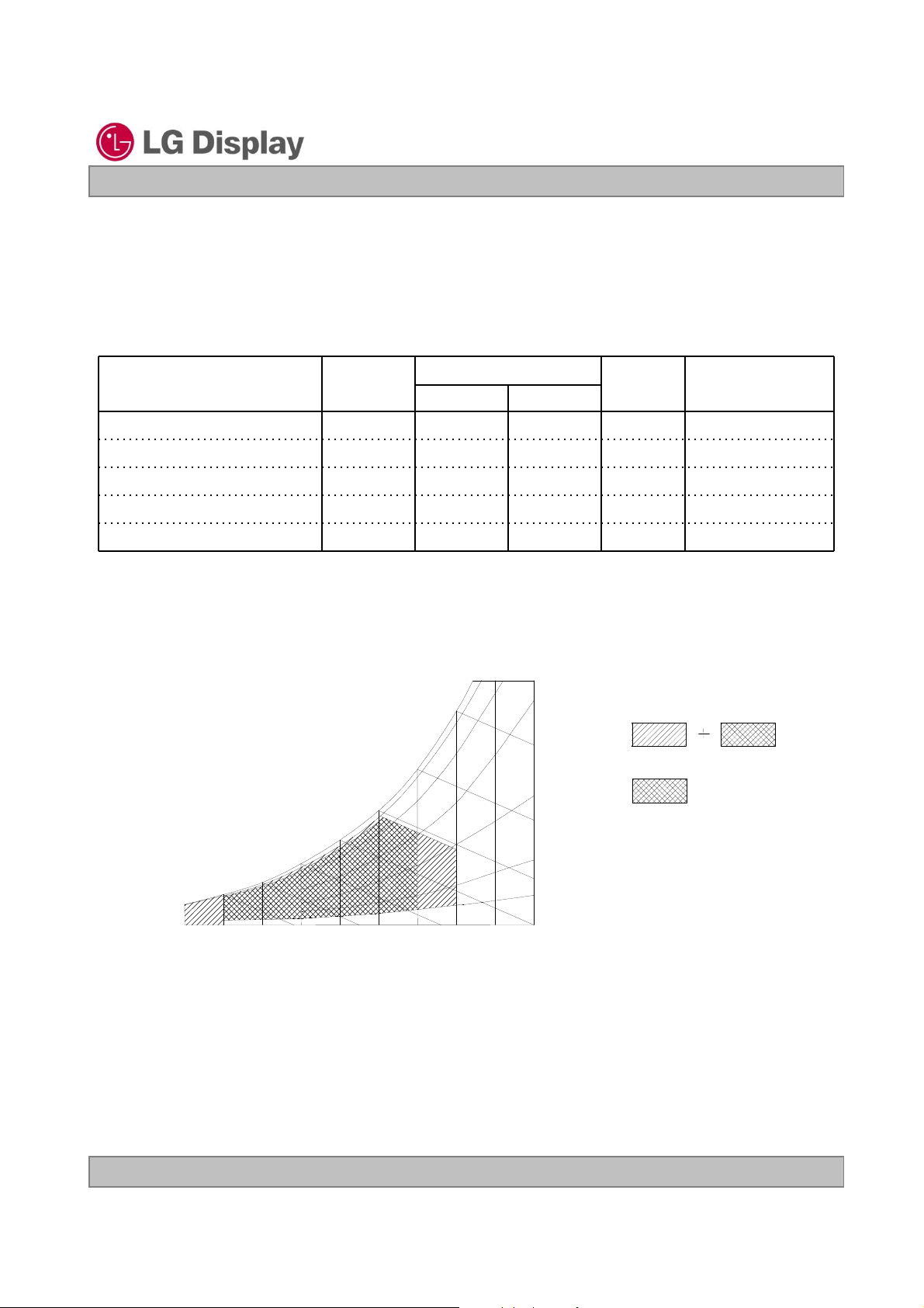
Note : 1. Temperature and relative humidity range are shown in the figure below.
Wet bulb temperature should be 39
Wet Bulb
Temperature [℃]
30
20
10
0
C Max, and no condensation of water.
90% 80%
60
50
40
60%
Humidity[(%)RH]
40%
20%
10%
Storage
Operation
-20
10
20 30 40 50
60 70 800
Dry Bulb Temperature [℃]
Ver. 1.0 Dec. 15. 2009
5/ 31
Page 6
LP140WD1
Liquid Crystal Display
Product Specification
3. Electrical Specifications
3-1. Electrical Characteristics
The LP140WD1 requires two power inputs. The first logic is employed to power the LCD electronics and to
drive the TFT array and liquid crystal. The second backlight is the input about LED BL with LED Driver.
Table 2. ELECTRICAL CHARACTERISTICS
Parameter Symbol
Unit Notes
Min Typ Max
LOGIC :
Values
Power Supply Input Voltage V
Power Supply Input Current Mosaic I
Power Consumption P
Power Supply Inrush Current I
LVDS Impedance Z
CC 3.0 3.3 3.6 V 1
CC
CC - 1.45 1.68 W 2
CC_P - - 2000 mA 3
LVDS 90 100 110
370 440 510
mA 2
Ω
BACKLIGHT : ( with LED Driver)
LED Power Input Voltage V
LED Power Input Current I
LED Power Consumption P
LED Power Inrush Current I
LED 7.0 12.0 20.0 V 5
LED - 297 315 mA 6
LED - 3.56 3.78 W 6
LED_P - - 2000 mA 7
PWM Duty Ratio 6 - 100 % 8
PWM Jitter
PWM Impedance Z
-
PWM 20 40 60 kΩ
0-0.3%9
4
PWM Frequency F
PWM High Level Voltage V
PWM Low Level Voltage V
LED_EN Impedance Z
LED_EN High Voltage
LED_EN Low Voltage
PWM 200 - 1000 Hz 10
PWM_H
PWM_L
PWM 20 40 60 kΩ
LED_EN
V
_H
V
LED_EN
_L
3.0 - 5.3 V
0-0.5V
3.0 - 5.3 V
0-0.5V
Life Time 12,000 - - Hrs 11
Ver. 1.0 Dec. 15. 2009
6/ 31
Page 7
Liquid Crystal Display
Product Specification
Note)
1. The measuring position is the connector of LCM and the test conditions are under 25℃, fv = 60Hz,
Black pattern.
2. The specified Icc current and power consumption are under
the Vcc = 3.3V , 25℃, fv = 60Hz condition whereas Mosaic pattern
is displayed and fv is the frame frequency.
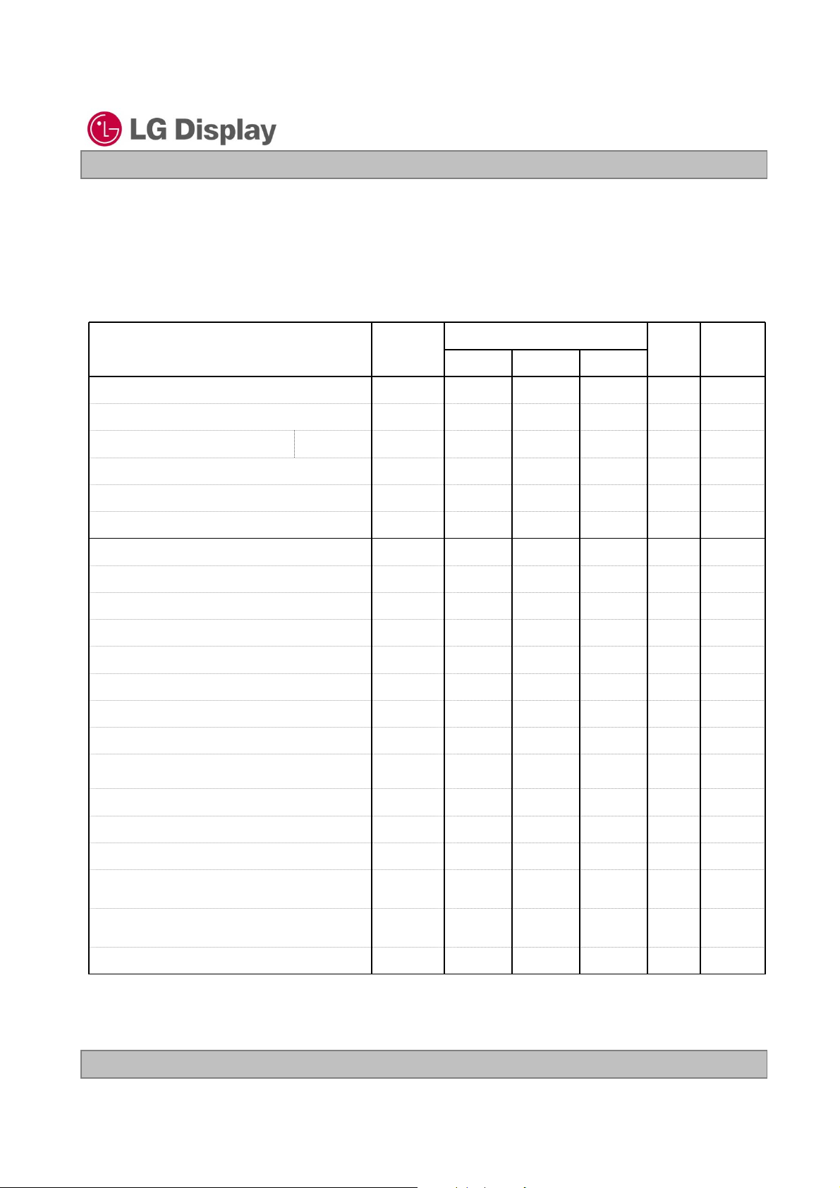
3. The below figures are the measuring Vcc condition and the Vcc control block LGD used.
The Vcc condition is same the minimum of T1 at Power on sequence.
LP140WD1
Rising time
Vcc
0V
10%
90%
3.3V
0.5ms
4. This impedance value is needed to proper display and measured form LVDS Tx to the mating connector.
5. The measuring position is the connector of LCM and the test conditions are under 25℃.
6. The current and power consumption with LED Driver are under the Vled = 12.0V , 25℃, Dimming of
Max luminance whereas White pattern is displayed and fv is the frame frequency.
7. The below figures are the measuring Vled condition
and the Vled control block LGD used.
VLED control block is sa me with V cc c o ntr ol bl oc k.
Rising time
V
LED
0V
10%
90%
12.0V
0.5ms
8. The operation of LED Driver below minimum dimming ratio may cause flickering or reliability issue.
9. If Jitter of PWM is bigger than maximum. It may cause flickering.
10. This Spec. is not effective at 100% dimming ratio as an exception because it has DC level equivalent
to 0Hz. In spite of acceptable range as defined, the PWM Frequency should be fixed and stable for
more consistent brightness control at any specific level desired.
11. The life time is determined as the time at which the typical brightness of LCD is 50% compare to that of
initial value at the typical LED current. These LED backlight has 6 strings on it and the typical current
of LED’s string is base on 20mA.
Ver. 1.0 Dec. 15. 2009
7/ 31
Page 8
LP140WD1
Liquid Crystal Display
Product Specification
3-2. Interface Connections
This LCD employs two interface connections, a 40 pin connector is used for the module electronics interface
and the other connector is used for the integral backlight system.
The electronics interface connector is a model CABLINE-VS RECE ASS’Y manufactured by I-PEX.
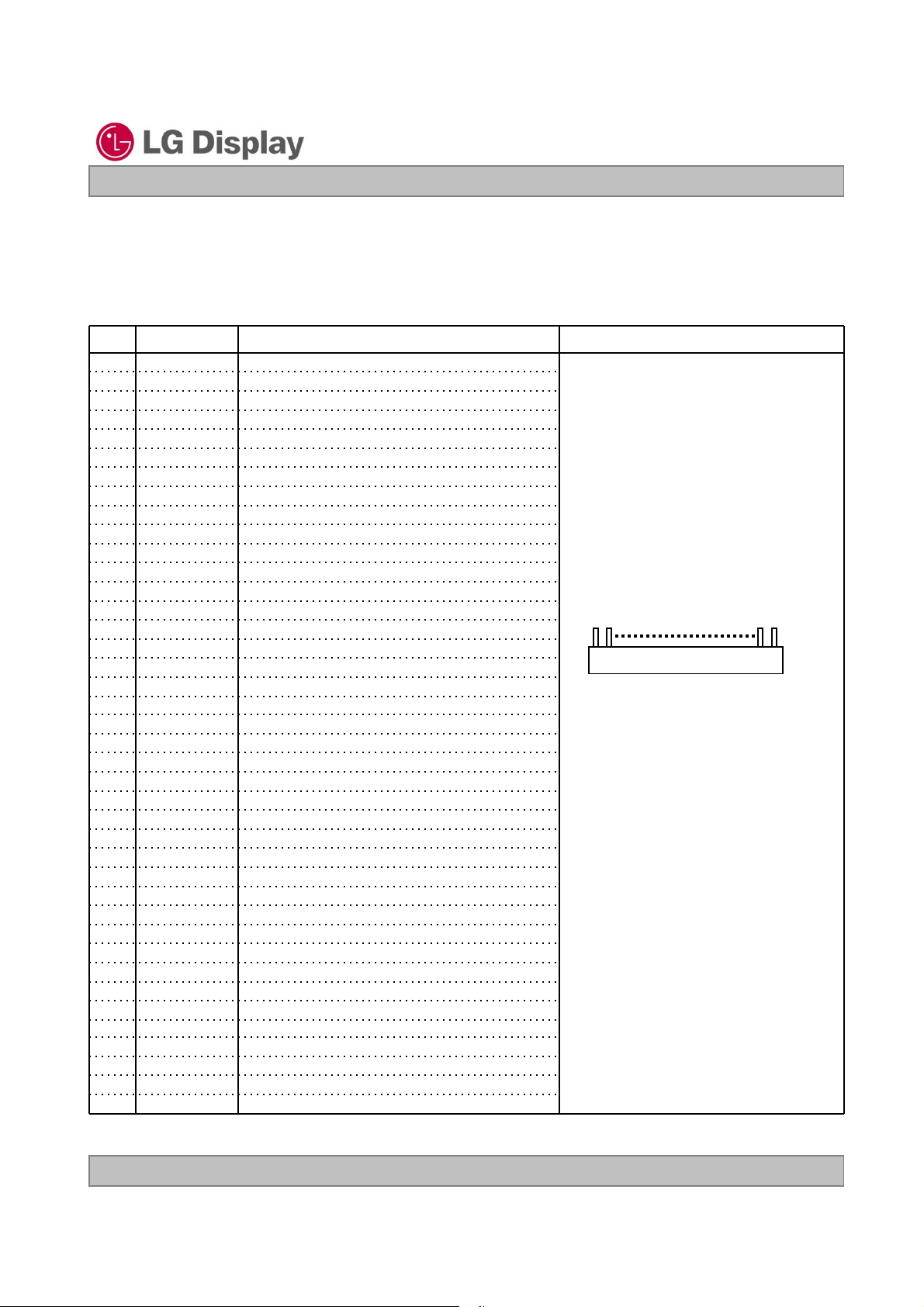
Table 3. MODULE CONNECTOR PIN CONFIGURATION (CN1)
Pin Symbol Description Notes
1 NC No Connection (Reserved for supplier)
2 VCC Power Supply, 3.3V Typ.
3 VCC Power Supply, 3.3V Typ.
4 V EEDID DDC 3.3V power
5 NC No Connection
6 Clk EEDID DDC Clock
7 DATA EEDID DDC Data
8 Odd_R
9 Odd_R
0- Negative LVDS differential data input
IN
0+ Positive LVDS differential data input
IN
10 GND Ground
11 Odd_R
12 Odd_R
1- Negative LVDS differential data input
IN
1+ Positive LVDS differential data input
IN
13 GND Ground
14 Odd_R
15 Odd_R
2- Negative LVDS differential data input
IN
2+ Positive LVDS differential data input
IN
16 GND Ground
17 Odd_CLKIN- Negative LVDS differential clock input
18 Odd_CLKIN+ Positive LVDS differential clock input
19 GND Ground
20 Even_R
21 Even_R
0- Negative LVDS differential data input
IN
0+ Positive LVDS differential data input
IN
19 GND Ground
23 Even_R
24 Even_R
1- Negative LVDS differential data input
IN
1+ Positive LVDS differential data input
IN
19 GND Ground
26 Even_R
27 Even_R
2- Negative LVDS differential data input
IN
2+ Positive LVDS differential data input
IN
19 GND Ground
29 Even_CLKIN- Negative LVDS differential clock input
30 Even_CLKIN+ Positive LVDS differential clock input
31
32
33
34
35
36
37
38
39
40
VLED_GND LED Ground
VLED_GND LED Ground
VLED_GND LED Ground
NC No Connection (Reserved)
PWM PWM for luminance control
LED_EN Backlight On/Off Control
NC No Connection (Reserved)
VLED LED Power Supply 6V-20V
VLED LED Power Supply 6V-20V
VLED LED Power Supply 6V-20V
1, Interface chips
1.1 LCD : SW, SW0617 (LCD Controller)
including LVDS Receiver
1.2 System : THC63LVDF823A
or equivalent
* Pin to Pin compatible with LVDS
2. Connector
2.1 LCD : CABLINE-VS(20455-040E-XX , I-PEX
or its compatibles
2.2 Mating : CABLINE-VS PLUG CABLE
ASS’Y or equivalent.
2.3 Connector pin arrangement
40
1
[LCD Module Rear View]
Ver. 1.0 Dec. 15. 2009
8/ 31
Page 9
Product Specification
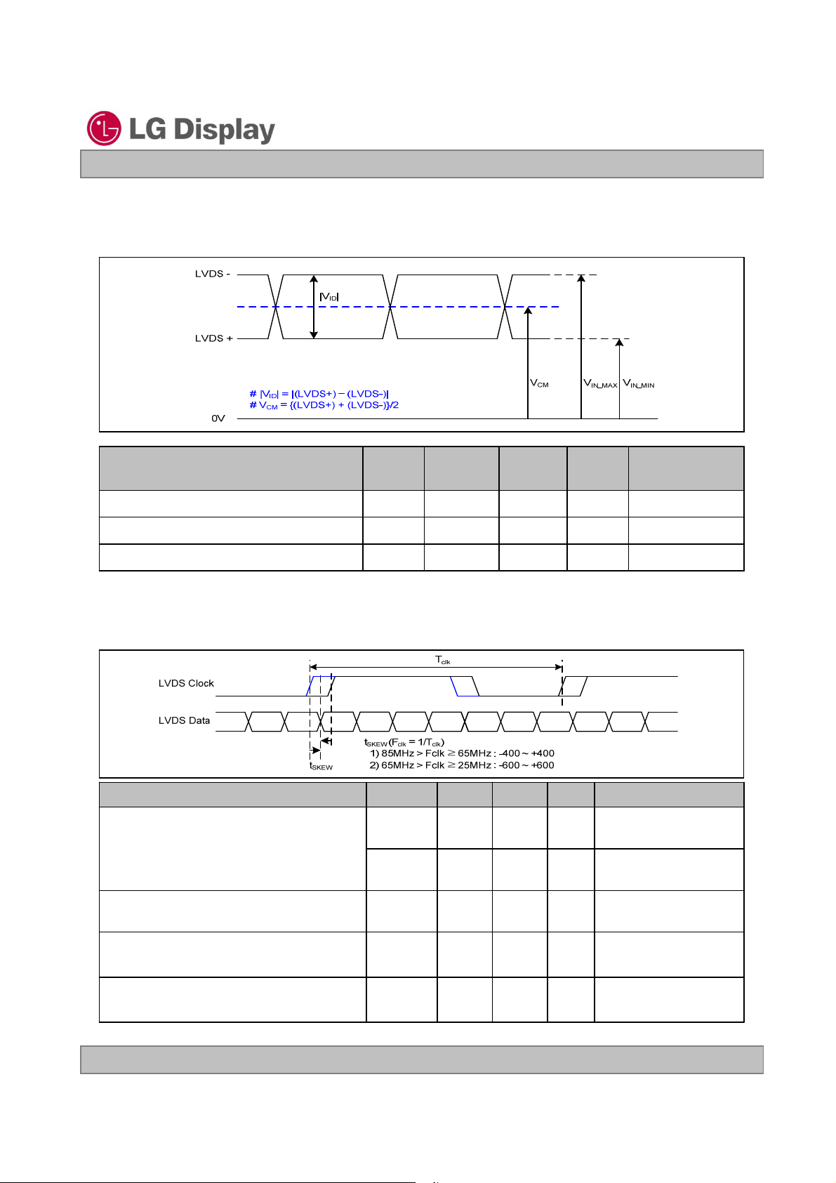
3-3. LVDS Signal Timing Specifications
3-3-1. DC Specification
LP140WD1
Liquid Crystal Display
Description
LVDS Differential Voltage |V
LVDS Common mode Voltage V
LVDS Input Voltage Range V
3-3-2. AC Specification
Description Symbol Min Max Unit Notes
LVDS Clock to Data Skew Margin
Symb
ol
| 100 600 mV -
ID
CM
IN
t
SKEW
t
SKEW
Min Max Unit Notes
0.6 1.8 V -
0.3 2.1 V -
- 400 + 400 ps
- 600 + 600 ps
85MHz > Fclk ≥
65MHz > Fclk ≥
65MHz
25MHz
LVDS Clock to Clock Skew Margin (Even
to Odd)
Maximum deviation
of input clock frequency during SSC
Maximum modulation frequency
of input clock during SSC
Ver. 1.0 Dec. 15. 2009
t
SKEW_EO
F
DEV
F
MOD
-1/7 + 1/7 T
clk
-
- ± 3% -
-200KHz -
9/ 31
Page 10
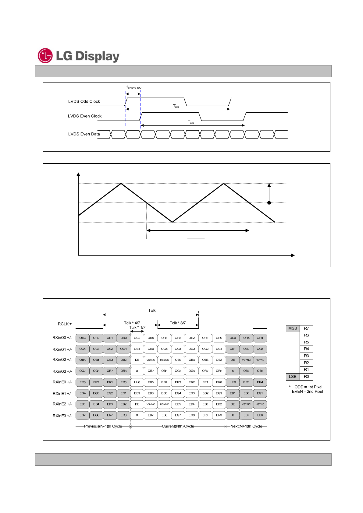
Freq.
F
max
F
center
F
min
Product Specification
< Clock skew margin between channel >
LP140WD1
Liquid Crystal Display
F
* F
center
DEV
3-3-3. Data Format
1) LVDS 2 Port
1
F
MOD
< Spread Spectrum >
Time
< LVDS Data Format >
Ver. 1.0 Dec. 15. 2009
10 / 31
Page 11

LP140WD1
Liquid Crystal Display
Product Specification
3-4. Signal Timing Specifications
This is the signal timing required at the input of the User connector. All of the interface signal timing should be
satisfied with the following specifications and specifications of LVDS Tx/Rx for its proper operation.
Table 4. TIMING TABLE
ITEM Symbol Min Typ Max Unit Note
DCLK Frequency f
Period
Hsync
Width t
Width-Active t
Period t
Vsync
Width-Active t
Horizontal back porch t
Data
Enable
Horizontal front porch t
Vertical back porch t
Vertical front porch t
CLK
t
HP
WH
WHA
VP
WV
WVA
HBP
HFP
VBP
VFP
- 53.9 - MHz
896 960 992
32 48 56
800 800 800
910 936 960
35 8
900 900 900
24 32 40
40 80 96
52836
23 5
tCLK
tHPWidth t
tCLK
tHP
Note)
1. In this documentation, all reliabilities are specified for timing spe cification bas ed on refresh rate of 60Hz.
However, LP140WD1 has a good actual performance even at lower refresh rate( eg. 40Hz or 50Hz) for
power saving mode, whereas LP140WD1 is secured only for function under lower refresh rate.
60Hz at Normal mode, 50Hz ,40 Hz at Power save mode. Don’t care Flicker level (power save mode).
3-5. Signal Timing Waveforms
High: 0.7VCC
Condition : VCC =3.3V
Data Enable, Hsync, Vsy n c
Low: 0.3VCC
DCLK
Hsync
t
tCLK
WH
t
HBP
0.5 Vcc
t
HP
tWHA
Data Enable
t
VP
t
WV
Vsync
t
VBP
tWVA
Data Enable
Ver. 1.0 Dec. 15. 2009
t
HFP
t
VFP
11 / 31
Page 12

LP140WD1
Liquid Crystal Display
Product Specification
3-6. Color Input Data Reference
The brightness of each prima ry color (r ed,green and b lue) is based on the 6-bit gray sca le data input for the
color ; the higher the binary input, the brighter the color. The table below provides a reference for color
versus data input.
Table 5. COLOR DATA REFERENCE
Input Color Data
Basic
Color
RED
GREEN
BLUE
Color
Black
Red
Green
Blue
Cyan
Magenta
Yellow
White
RED (00)
RED (01)
…
RED (62)
RED (63)
GREEN (00)
GREEN (01)
...
GREEN (62)
GREEN (63)
BLUE (00)
BLUE (01)
…
BLUE (62)
BLUE (63)
RED
MSB LSB
R5 R4 R3 R2 R1 R0 G5 G4 G3 G2 G1 G0 B5 B4 B3 B2 B1 B0
0 0 0 0 0 0 0 0 0 0 0 0 0 0 0 0 0 0
1 1 1 1 1 1 0 0 0 0 0 0 0 0 0 0 0 0
0 0 0 0 0 0 1 1 1 1 1 1 0 0 0 0 0 0
0 0 0 0 0 0 0 0 0 0 0 0 1 1 1 1 1 1
0 0 0 0 0 0 1 1 1 1 1 1 1 1 1 1 1 1
1 1 1 1 1 1 0 0 0 0 0 0 1 1 1 1 1 1
1 1 1 1 1 1 1 1 1 1 1 1 0 0 0 0 0 0
1 1 1 1 1 1 1 1 1 1 1 1 1 1 1 1 1 1
0 0 0 0 0 0 0 0 0 0 0 0 0 0 0 0 0 0
0 0 0 0 0 1 0 0 0 0 0 0 0 0 0 0 0 0
………
1 1 1 1 1 0 0 0 0 0 0 0 0 0 0 0 0 0
1 1 1 1 1 1 0 0 0 0 0 0 0 0 0 0 0 0
0 0 0 0 0 0 0 0 0 0 0 0 0 0 0 0 0 0
0 0 0 0 0 0 0 0 0 0 0 1 0 0 0 0 0 0
………
0 0 0 0 0 0 1 1 1 1 1 0 0 0 0 0 0 0
0 0 0 0 0 0 1 1 1 1 1 1 0 0 0 0 0 0
0 0 0 0 0 0 0 0 0 0 0 0 0 0 0 0 0 0
0 0 0 0 0 0 0 0 0 0 0 0 0 0 0 0 0 1
………
0 0 0 0 0 0 0 0 0 0 0 0 1 1 1 1 1 0
0 0 0 0 0 0 0 0 0 0 0 0 1 1 1 1 1 1
MSB LSB
GREEN
BLUE
MSB LSB
Ver. 1.0 Dec. 15. 2009
12 / 31
Page 13

3-7. Power Sequence
Power Supply Input
VCC
0V
Product Specification
90%
LP140WD1
Liquid Crystal Display
90%
10%10%
Interface Signal, V
i
LVDS
LED on/off control Signal
LED_EN
Dimming control signal
Of LED BL
PWM
LED input Voltage
VLED
Logic
Parameter
T
1
T
2
T
3
T
4
T
5
T
6
T
7
Min. Typ. Max.
0.5 - 10 ms
0-50ms
0-50ms
400 - - ms
200 - - ms
200 - - ms
3-10ms
Value
T
T
1
2
Valid Data
0V
T
5
0V (Off)
T
9
Valid Data
0V (Low)
T
8
90%
0V
10%
T
12
Table 6. POWER SEQUENCE TABLE
Units
LED
Parameter
T
8
T
9
T
10
T
11
T
12
T
T
3
7
T
6
T
10
T
11
90%
T
4
Value
Units
Min. Typ. Max.
10 - - ms
0--ms
0--ms
10 - - ms
0.5 - - ms
Note)
1. Do not insert the mating cable when system turn on.
2. Valid Data have to meet “3-3. LVDS Signal Timing Specifications”
3. LVDS, LED_EN and PWM need to pull-down condition on invalid status.
4. LGD recommend the rising sequence of VLED after the Vcc and valid status of LVDS turn on.
Ver. 1.0 Dec. 15. 2009
13 / 31
Page 14

LP140WD1
Liquid Crystal Display
Product Specification
4. Optical Specification
Optical characteristics are deter mined after the unit has been ‘ON ’ and stable fo r approximately 30 minutes in
a dark environment at 25
at a viewing angle of
FIG. 1 presents additional information concerning the measurement equipment and method.
C. The values specified are at an approximate distance 50cm from the LC D su rface
and equal to 0.
FIG. 1 Optical Characteristic Measurement Equipment and Method
Optical Stage(x,y)
LCD Module
Pritchard 880 or
equivalent
50cm
Table 7. OPTICAL CHARACTERISTICS
Ta=25C, VCC=3.3V, fV=60Hz, f
Parameter Symbol
Min Typ Max
Values
Contrast Ratio CR 300 - - 1
Surface Luminance, white L
Luminance Variation
Response Time
TrR+ Tr
WH
WHITE
170 200 - cd/m
--1.6 3
D
-816ms 4
Color Coordinates
RED RX
RY
GREEN GX
GY
BLUE BX
BY
WHITE WX
WY
0.574 0.604 0.634
0.326 0.356 0.386
0.296 0.326 0.356
0.551 0.581 0.611
0.119 0.149 0.179
0.023 0.053 0.083
0.283 0.313 0.343
0.299 0.329 0.359
Viewing Angle 5
x axis, right(=0) r 40 - - degree
x axis, left (=180) l 40 - - degree
y axis, up (=90) u 10 - - degree
y axis, down (=270) d 30 - - degree
Gray Scale 6
= 53.9MHz, I
CLK
Units Notes
2
= 20 mA
LED
2
Ver. 1.0 Dec. 15. 2009
14 / 31
Page 15

Liquid Crystal Display
Product Specification
Note)
1. Contrast Ratio(CR) is defined mathematically as
Surface Luminance with all white pixels
Contrast Ratio =
Surface Luminance with all black pixels
2. Surface luminance is the average of 5 point across the LCD surface 50cm from the surface with
all pixels displaying white. For more information see FIG 1.
L
= Average(L1,L2, … L5)
WH
LP140WD1
3. The variation in surface luminance , The panel total variation (
) is determined by measuring L
WHITE
N
at each test position 1 through 13 and then defined as followed numerical formula.
For more information see FIG 2.
Maximum(L
WHITE
=
Minimum(L
4. Response time is the time required for the display to transition from white to black (rise time, Tr
from black to white(Decay Time, Tr
). For additional information see FIG 3.
D
1,L2
1,L2
, … L13)
, … L13)
) and
R
5. Viewing angle is the angle at which the contrast ratio is greater than 10. The angles are determined
for the horizontal or x axis and the vertical or y axis with respect to the z axis which is normal to the
LCD surface. For more information see FIG 4.
6. Gray scale specification * f
= 60Hz
V
Gray Level Luminance [%] (Typ)
L0 0
L7 5.8
L15 12.7
L23 21.4
L31 33.2
L39 48.3
L47 66.5
L55 87.0
L63 100
Ver. 1.0 Dec. 15. 2009
15 / 31
Page 16

Product Specification
FIG. 2 Luminance
<measuring point for surface luminance & measuring point for luminance variation>
H
LP140WD1
Liquid Crystal Display
A
C
L6
L7
D
L8
H,V : ACTIVE AREA
A : H/4 mm
B : V/4 mm
L2
L3
C : 10 mm
D : 10 mm
B
V
L9
L1
L10
POINTS : 13 POINTS
Center Point
L4 L5
L11 L13
FIG. 3 Response Time
The response time is defined as the following figure and shall be measured by switching the input signal
for “black” and “white”.
L12
Tr
R
%
100
90
Optical
Response
10
0
white
Ver. 1.0 Dec. 15. 2009
black
Tr
D
white
16 / 31
Page 17

LP140WD1
Liquid Crystal Display
Product Specification
5. Mechanical Characteristics
The contents provide general mechanical characteristics for the model LP140WD1. In addition the figures
in the next page are detailed mechanical drawing of the LCD.
Horizontal 323.5 0.5mm
Outline Dimension
Bezel Area
Active Display Area
Weight 375g (Max.)
Surface Treatment
Vertical 192.0 0.5mm
Thickness 5.2mm (max)
Horizontal (VESA Standard) 316.0 0.5mm
Vertical (VESA Standard) 177.4 0.5mm
Horizontal 309.60 mm
Vertical 174.15 mm
Anti-glare treatment of the front polarizer
Ver. 1.0 Dec. 15. 2009
17 / 31
Page 18

Product Specification
LP140WD1
Liquid Crystal Display
<FRONT VIEW>
Note) Unit:[mm], General tolerance:
0.5mm
Ver. 1.0 Dec. 15. 2009
18 / 31
Page 19

Product Specification
LP140WD1
Liquid Crystal Display
<REAR VIEW>
Note) Unit:[mm], General tolerance:
0.5mm
Ver. 1.0 Dec. 15. 2009
19 / 31
Page 20

Product Specification
[ DETAIL DESCRIPTION OF SIDE MOUNTING SCREW ]
LP140WD1
Liquid Crystal Display
* Mounting Screw Length (A)
= 2.0(Min) / 2.5(Max)
* Mounting Screw Hole Depth (B)
= 2.5(Min)
* Mounting hole location : 3.1(typ.)
* Torque : 2.0 kgf.cm(Max)
(Measurement gauge : torque meter)
Notes : 1. Screw plated through the method of non-electrolytic nickel plating is preferred
to reduce possibility that results in vertical and/or horizontal line defect due to
the conductive particles from screw surface.
Ver. 1.0 Dec. 15. 2009
20 / 31
Page 21

Product Specification
LGD Proposal for system cover design.(Appendix)
LP140WD1
Liquid Crystal Display
1
Gap check for securing the enough gap between LCM
and System cover.
Max Thickness
Sponge
LCM Reflector Side
System Cover
A Boundary Line
1.Rear side of LCM is sensitive against external stress,and previous check
about interference is highly needed.
Define
2.In case there is something from system cover comes into the boundary
above,mechanical interference may cause the FOS defects.
(Eg:Ripple,White spot..)
2 Check if antenna cable is sufficiently apart from T-CON of LCD Module.
Define
NO GOOD
GOOD
1.If system antenna is overlapped with T-CON,it might be cause the noise.
Ver. 1.0 Dec. 15. 2009
21 / 31
Page 22

Product Specification
LGD Proposal for system cover design.
LP140WD1
Liquid Crystal Display
3
Gap check for securing the enough gap between LCM
and System hinge.
LCM Reflector Side
Side Mount Screw Hole (4ea)
1.At least 2.0mm of gap needs to be secured to prevent the shock
Define
related defects.
Hinge
GAP:Min2.0mm
(“I” TYPE)
COF
(D-IC)
(“L” TYPE)
2.”L” type of hinge is recommended than “I” type under shock test.
4
Checking the path of the System wire.
LCM Reflector Side
Ok Bad
1.COF area needs to be handled with care.
2.GOOD Wire path design to system side.
Define
OK Wire path is located between COFs.
BADWire path overlapped with COF area.
Ver. 1.0 Dec. 15. 2009
Good
22 / 31
Page 23

Product Specification
LGD Proposal for system cover design.
5 Using a bracket on the top of LCM is not recommended.
bracket
LP140WD1
Liquid Crystal Display
With bracket Without bracket
1.Condition without bracket is good for mechanical noise,and can minimize
the light leakage from deformation of bracket.
Define
2.The results shows that there is no difference between the condition
with or without bracket.
6 Securing additional gap on CNT area..
A
A~A-1
cut
System cover inner side.
User connector
area.
A-1
User connector
Cable pathway.
FPC:Flexible Printed Circuit.
1.CNT area is specially sensitive against external stress,and additional
Define
gap by cutting on system cover will be helpful on removing the Ripple.
2.Using a thinner CNT will be better. (eg: FPC type)
Ver. 1.0 Dec. 15. 2009
23 / 31
Page 24

Product Specification
6. Reliability
Environment test condition
No. Test Item Conditions
1 High temperature storage test Ta= 60C, 240h
2 Low temperature storage test Ta= -20C, 240h
3 High temperature operation test Ta= 50C, 50%RH, 240h
4 Low temperature operation test Ta= 0C, 240h
5 Vibration test (non-operating) Sine wave, 10 ~ 500 ~ 10Hz, 1.5G, 0.37oct/min
3 axis, 1hour/axis
6 Shock test (non-operating) Half sine wave, 180G, 2ms
one shock of each six faces(I.e. run 180G 2ms
for all six faces)
LP140WD1
Liquid Crystal Display
7 Altitude operating
storage / shipment
{ Result Evaluation Criteria }
There should be no change which might affect the practical display function when the display quality
test is conducted under normal operating condition.
0 ~ 10,000 feet (3,048m) 24Hr
0 ~ 40,000 feet (12,192m) 24Hr
Ver. 1.0 Dec. 15. 2009
24 / 31
Page 25

LP140WD1
Liquid Crystal Display
Product Specification
7. International Standards
7-1. Safety
a) UL 60950-1, Second Edition, Underwriters Laboratories Inc.
Information Technology Equipment - Safety - Part 1 : General Requirements.
b) CAN/CSA C22.2 No.60950-1-07, Second Edition, Canadian Standards Association.
Information Technology Equipment - Safety - Part 1 : General Requirements.
c) EN 60950-1:2006 + A11:2009, European Committee for Electrotechnical Standardization (CENELEC).
Information Technology Equipment - Safety - Part 1 : General Requirements.
d) IEC 60950-1:2005, Second Edition, The International Electrotechnical Commission (IEC).
Information Technology Equipment - Safety - Part 1 : General Requirements.
7-2. EMC
a) ANSI C63.4 “American National Standard for Methods of Measurement of Radio-Noise
Emissions from Low-Voltage Electrical and Electronic Equipment in the Range of 9 kHz to 40 GHz.”
American National Standards Institute (ANSI), 2003.
b) CISPR 22 “Information technology equipment – Radio disturbance characteristics – Limit and
methods of measurement." International Special Committee on Radio Interference
(CISPR), 2005.
c) CISPR 13 “Sound and television broadcast receivers and associated equipment – Radio disturbance
characteristics – Limits and method of measurement." International Special Committee on Radio
Interference (CISPR), 2006.
7-3. Environment
a) RoHS, Directive 2002/95/EC of the European Parliament and of the council of 27 January 2003
Ver. 1.0 Dec. 15. 2009
25 / 31
Page 26

Product Specification
8. Packing
8-1. Designation of Lot Mark
a) Lot Mark
ABCDEFGHI JKLM
A,B,C : SIZE(INCH) D : YEAR
E : MONTH F ~ M : SERIAL NO.
Note
1. YEAR
LP140WD1
Liquid Crystal Display
Year
Mark
2. MONTH
Month
Mark
b) Location of Lot Mark
Serial No. is printed on the label. The label is attached to the backside of the LCD module.
This is subject to change without prior notice.
8-2. Packing Form
a) Package quantity in one box : 30 pcs
b) Box Size : 490mm X 390mm X 256 mm
2006720078200892009
6
Jun7Jul8Aug9Sep
6
321
200452005
4
Apr5May
4
200320022001
2010
0
Oct
A
Nov
B
DecMarFebJan
C321
Ver. 1.0 Dec. 15. 2009
26 / 31
Page 27

LP140WD1
Liquid Crystal Display
Product Specification
9. PRECAUTIONS
Please pay attention to the followings when you use this TFT LCD module.
9-1. MOUNTING PRECAUTIONS
(1) You must mount a module using holes arranged in four corners or four sides.
(2) You should consider the mounting structure so that uneven force (ex. Twisted stress) is not applied to the
module. And the case on which a module is mounted s hould have sufficient strength so that external
force is not transmitted directly to the module.
(3) Please attach the surface transparent protective plate to the surface in order to protect the polarizer.
Transparent protective plate should have sufficient strength in order to the resist external force.
(4) You should adopt radiation structure to satisfy the temperature specification.
(5) Acetic acid type and chlorine type materials for the cover case are not des irable because the former
generates corrosive gas of attacking the polarizer at high temper ature and the latter causes cir cuit break
by electro-chemical reaction.
(6) Do not touch, push or rub the exposed polarizers with glass, tweezers or anything harder than HB
pencil lead. And please do not rub with dust clothes with chemical treatment.
Do not touch the surface of polarizer for bare hand or greasy cloth.(Some cosmetics are detrimental
to the polarizer.)
(7) When the surface becomes dusty, please wipe gently with absorbent cotton or other soft mater ials like
chamois soaks with petroleum benzene. Normal-hexane is recommended for cleaning the adhesives
used to attach front / rear polarizers. Do not use acetone, toluene and alcohol because they cause
chemical damage to the polarizer.
(8) Wipe off saliva or water drops as soon as possible. Their long time contact with polarizer causes
deformations and color fading.
(9) Do not open the case because inside circuits do not have sufficient strength.
9-2. OPERATING PRECAUTIONS
(1) The spike noise causes the mis-operation of circuits. It should be lower than following voltage :
V=± 200mV(Over and under shoot voltage)
(2) Response time depends on the temperature.(In lower temperature, it becomes longer.)
(3) Brightness depends on the temperature. (In lower temperature, it becomes lower.)
And in lower temperature, response time(required time that brightness is stable after tu rned on ) beco mes
longer.
(4) Be careful for condensation at sudden temperature change. Condensation makes damage to polarizer or
electrical contacted parts. And after fading condensation, smear or spot will occur.
(5) When fixed patterns are displayed for a long time, remnant image is likely to occur.
(6) Module has high frequency cir cuits. Sufficient suppression to the elec tromagnetic interference shall be
done by system manufacturers. Grounding and shielding methods may be important to minimized the
interference.
Ver. 1.0 Dec. 15. 2009
27 / 31
Page 28

LP140WD1
Liquid Crystal Display
Product Specification
9-3. ELECTROSTATIC DISCHARGE CONTROL
Since a module is composed of electronic circuits, it is not strong to elec trosta tic di scharge. Make cer tain that
treatment persons are connected to ground through wrist band etc. And don’t touch interface pin directly.
9-4. PRECAUTIONS FOR STRONG LIGHT EXPOSURE
Strong light exposure causes degradation of polarizer and color filter.
9-5. STORAGE
When storing modules as spares for a long time, the following precautions are necessary.
(1) Store them in a dark place. Do not expose the module to sunlight or fluorescent light. Keep the
temperature between 5C and 35C at normal humidity.
(2) The polarizer surface should not come in contact with any other object.
It is recommended that they be stored in the container in which they were shipped.
9-6. HANDLING PRECAUTIONS FOR PROTECTION FILM
(1) When the protection film is peeled off, static electricity is generated between the film and polarizer.
This should be peeled off slowly and carefully by people who are electrically grounded and with well
ion-blown equipment or in such a condition, etc.
(2) The protection film is attached to the polarizer with a small amount of glue. If some stress is applied
to rub the protection film against the polarizer during the time you peel off the film, the glue is apt to
remain on the polarizer.
Please carefully peel off the protection film without rubbing it against the polarizer.
(3) When the module with protection film attached is stored for a long time, sometimes there remains a
very small amount of glue still on the polarizer after the protection film is peeled off.
(4) You can remove the glue easily. When the glue remains on the polarizer surface or its vestige is
recognized, please wipe them off with absorbent cotton waste or other soft material like chamois
soaked with normal-hexane.
Ver. 1.0 Dec. 15. 2009
28 / 31
Page 29

LP140WD1
Liquid Crystal Display
Product Specification
APPENDIX A. Enhanced Extended Display Identification Data (EEDIDTM) 1/3
Ver. 1.0 Dec. 15. 2009
29 / 31
Page 30

LP140WD1
Liquid Crystal Display
Product Specification
APPENDIX A. Enhanced Extended Display Identification Data (EEDIDTM) 2/3
Ver. 1.0 Dec. 15. 2009
30 / 31
Page 31

LP140WD1
Liquid Crystal Display
Product Specification
APPENDIX A. Enhanced Extended Display Identification Data (EEDIDTM) 3/3
Ver. 1.0 Dec. 15. 2009
31 / 31
 Loading...