

Page 1
THE INFORMATION CONTAINED HEREIN IS THE PROPERTY OF APPLE, INC. THE POSSESSOR AGREES TO THE FOLLOWING:
(i) TO MAINTAIN THIS DOCUMENT IN CONFIDENCE (ii) NOT TO REPRODUCE OR COPY IT (iii) NOT TO REVEAL OR PUBLISH IT IN WHOLE OR IN PART
Apple Inc.
Size: Letter
Scale: NONE
Page 1 of 67
Title: ERIS, DSPL, LCD MODULE, LGD, X34 DWG Number: 069-8326 ___Rev. B___
Revision
ECO#
Approved By
Date
Revision History
B
xxxxxx
Per ECO Approvals
08/14/2012
See Last Page for Revision History
LGD LCD Module Specification for X34
13.3” (2560X1600) TFT-LCD
Page 2
THE INFORMATION CONTAINED HEREIN IS THE PROPERTY OF APPLE, INC. THE POSSESSOR AGREES TO THE FOLLOWING:
(i) TO MAINTAIN THIS DOCUMENT IN CONFIDENCE (ii) NOT TO REPRODUCE OR COPY IT (iii) NOT TO REVEAL OR PUBLISH IT IN WHOLE OR IN PART
Apple Inc.
Size: Letter
Scale: NONE
Page 2 of 67
Title: ERIS, DSPL, LCD MODULE, LGD, X34 DWG Number: 069-8326 ___Rev. B___
Revision History
Revision
Date
ECO
Author
Comments
1
09/16/11
Eric Benson
Initial Engineering Release
2
12/12/11
Eric Benson
Light Leakage and Testing Updates
3
8/8/11
Eric Benson
Optical, Mechanical, and Testing Updates
4
4/24/12
Eric Benson
Optical, Mechanical, Grinding, Electrical, Reliability
Updates
5
5/28/12
Eric Benson
Optical, Electrical, Mechanical, Reliability Updates.
Removed light leakage requirement
6
6/7/2012
Eric Benson
Added LCD edge ink spec.
A
8/06/2012
Eric Benson
Production Release
B
8/14/2012
Eric Benson
Added V-Com tuning requirement. Transmittance minimum
updated.
Page 3

THE INFORMATION CONTAINED HEREIN IS THE PROPERTY OF APPLE, INC. THE POSSESSOR AGREES TO THE FOLLOWING:
(i) TO MAINTAIN THIS DOCUMENT IN CONFIDENCE (ii) NOT TO REPRODUCE OR COPY IT (iii) NOT TO REVEAL OR PUBLISH IT IN WHOLE OR IN PART
Apple Inc.
Size: Letter
Scale: NONE
Page 3 of 67
Title: ERIS, DSPL, LCD MODULE, LGD, X34 DWG Number: 069-8326 ___Rev. B___
TABLE OF CONTENTS
!"! #$%&$'#(')$&*&%&+*&'#(',-*./&+0102-+'3.04-$205'""""""""""""""""""""""""""""""""""""""""""""""""""""""""""'6!
7"! 8&(&$&+*&',-*./&+09'"""""""""""""""""""""""""""""""""""""""""""""""""""""""""""""""""""""""""""""""""""""""""""""""""""""""""""""""""':!
;"! <&+&$1=',&9*$2>02-+'""""""""""""""""""""""""""""""""""""""""""""""""""""""""""""""""""""""""""""""""""""""""""""""""""""""""""""""""""'!?!
@"! A.+*02-+1='8&B.2$&/&+09'""""""""""""""""""""""""""""""""""""""""""""""""""""""""""""""""""""""""""""""""""""""""""""""""""""""""'!!!
@"!"! ,29>=15'C-%&='""""""""""""""""""""""""""""""""""""""""""""""""""""""""""""""""""""""""""""""""""""""""""""""""""""""""""""""""""""""""""""""""""""'!!!
@"7"! )2D&='E-+(2F.$102-+'""""""""""""""""""""""""""""""""""""""""""""""""""""""""""""""""""""""""""""""""""""""""""""""""""""""""""""""""""""""""""'!7!
@";"! )2D&=')20*4'"""""""""""""""""""""""""""""""""""""""""""""""""""""""""""""""""""""""""""""""""""""""""""""""""""""""""""""""""""""""""""""""""""""""""""'!7!
@"@"! 8&9-=.02-+'"""""""""""""""""""""""""""""""""""""""""""""""""""""""""""""""""""""""""""""""""""""""""""""""""""""""""""""""""""""""""""""""""""""""""""'!7!
@"G"! 8.HH2+F',2$&*02-+'""""""""""""""""""""""""""""""""""""""""""""""""""""""""""""""""""""""""""""""""""""""""""""""""""""""""""""""""""""""""""""'!7!
@"I"! J+0&$(1*&'1+%',$2K2+F'L*4&/ &'""""""""""""""""""""""""""""""""""""""""""""""""""""""""""""""""""""""""""""""""""""""""""""""""""""""'!;!
@"M"! A$-+0'L.$(1*&'N$&10/&+0'""""""""""""""""""""""""""""""""""""""""""""""""""""""""""""""""""""""""""""""""""""""""""""""""""""""""""""""""'!;!
G"! C&*41+2*1='8&B.2$&/&+09'""""""""""""""""""""""""""""""""""""""""""""""""""""""""""""""""""""""""""""""""""""""""""""""""""""""'!;!
G"!"! O+K&=->&',2/&+92-+9'1+%'N-=&$1+*&9'""""""""""""""""""""""""""""""""""""""""""""""""""""""""""""""""""""""""""""""""""""""'!;!
G"7"! 3*02K&'3$&1'""""""""""""""""""""""""""""""""""""""""""""""""""""""""""""""""""""""""""""""""""""""""""""""""""""""""""""""""""""""""""""""""""""""""""'!;!
G";"! C199'"""""""""""""""""""""""""""""""""""""""""""""""""""""""""""""""""""""""""""""""""""""""""""""""""""""""""""""""""""""""""""""""""""""""""""""""""""""""'!;!
G"@"! P+20'A=10+&99'""""""""""""""""""""""""""""""""""""""""""""""""""""""""""""""""""""""""""""""""""""""""""""""""""""""""""""""""""""""""""""""""""""""" '!;!
5.4.1.! Flatness!Measurement!Requirements!................................................................................................!13!
G"G"! OD>-9&%'3$&1'1+%'8&90$2*02-+9'""""""""""""""""""""""""""""""""""""""""""""""""""""""""""""""""""""""""""""""""""""""""""""""""""""'!;!
G"I"! O%F&'Q.1=205'8&B.2$&/&+09'""""""""""""""""""""""""""""""""""""""""""""""""""""""""""""""""""""""""""""""""""""""""""""""""""""""""""'!;!
5.6.1.! Surface!Finish!Requirements!..................................................................................................................!14!
5.6.2.! Edge!Defect!Requirements!.......................................................................................................................!15!
5.6.3.! Ground!Surface!Profile!...............................................................................................................................!16!
G"M"! )-=1$2R&$'O%F&'8&B.2$&/&+0'""""""""""""""""""""""""""""""""""""""""""""""""""""""""""""""""""""""""""""""""""""""""""""""""""""""""'!M!
G"6"! C&*41+2*1='L01*ST.>'""""""""""""""""""""""""""""""""""""""""""""""""""""""""""""""""""""""""""""""""""""""""""""""""""""""""""""""""""""""""'!6!
G":"! ,$2K&$'JE'C&*41+2*1='8&B.2$&/&+09'""""""""""""""""""""""""""""""""""""""""""""""""""""""""""""""""""""""""""""""""""""""""""'!6!
5.9.1.! Driver!IC!Edge!Quality!................................................................................................................................!18!
5.9.2.! Driver!IC!Top!Surface!Requirement!.....................................................................................................!19!
G"!?"! P+20'O%F&'J+S'8&B.2$&/&+0'""""""""""""""""""""""""""""""""""""""""""""""""""""""""""""""""""""""""""""""""""""""""""""""""""""""""'!:!
I"! N4&$/1='8&B.2$&/&+09'""""""""""""""""""""""""""""""""""""""""""""""""""""""""""""""""""""""""""""""""""""""""""""""""""""""""""""'!:!
M"! O=&*0$2*1='8&B.2$&/&+09'""""""""""""""""""""""""""""""""""""""""""""""""""""""""""""""""""""""""""""""""""""""""""""""""""""""""""'!:!
M"!"! U=-*S',21F$1/'"""""""""""""""""""""""""""""""""""""""""""""""""""""""""""""""""""""""""""""""""""""""""""""""""""""""""""""""""""""""""""""""""""'!:!
M"7"! ,29>=15')EU'L*4&/102*9'""""""""""""""""""""""""""""""""""""""""""""""""""""""""""""""""""""""""""""""""""""""""""""""""""""""""""""""""""'7?!
M";"! ,29>=15')EU'V15-.0'""""""""""""""""""""""""""""""""""""""""""""""""""""""""""""""""""""""""""""""""""""""""""""""""""""""""""""""""""""""""""'7!!
M"@"! 3*02K&'E-/>-+&+09'""""""""""""""""""""""""""""""""""""""""""""""""""""""""""""""""""""""""""""""""""""""""""""""""""""""""""""""""""""""""""'7!!
7.4.1.! Electrical!Interface!Requirements!........................................................................................................!21!
7.4.2.! Extended!Display!Identification!Data!(EDID)!Interface!..............................................................!22!
7.4.3.! Power!Supply!Requirements!..................................................................................................................!25!
7.4.4.! Signal!Timing!.................................................................................................................................................!25!
7.4.5.! Power!Requirements!(W/O!backlight)!...............................................................................................!27!
7.4.6.! Display!Pattern!Requirements!...............................................................................................................!27!
M"G"! )-W&$'-+T-(('9&B.&+*&'"""""""""""""""""""""""""""""""""""""""""""""""""""""""""""""""""""""""""""""""""""""""""""""""""""""""""""""""""""'76!
M"I"! X**'X-=01F&',$->'8&B.2$&/&+0'""""""""""""""""""""""""""""""""""""""""""""""""""""""""""""""""""""""""""""""""""""""""""""""""""""'76!
M"M"! Y&1$TA2&=%'Y-29&'""""""""""""""""""""""""""""""""""""""""""""""""""""""""""""""""""""""""""""""""""""""""""""""""""""""""""""""""""""""""""""""""'76!
M"6"! &,)'U20TO$$-$T810&'ZUO8['8&B.2$&/&+0'"""""""""""""""""""""""""""""""""""""""""""""""""""""""""""""""""""""""""""""""""""'76!
M":"! E#<'U20'O$$-$'810&'ZUO8['8&B.2$&/&+0'""""""""""""""""""""""""""""""""""""""""""""""""""""""""""""""""""""""""""""""""""""'76!
M"!?"! )$-F$1//1H=&'<1//1'L&002+F9'"""""""""""""""""""""""""""""""""""""""""""""""""""""""""""""""""""""""""""""""""""""""""""""""'76!
Page 4

THE INFORMATION CONTAINED HEREIN IS THE PROPERTY OF APPLE, INC. THE POSSESSOR AGREES TO THE FOLLOWING:
(i) TO MAINTAIN THIS DOCUMENT IN CONFIDENCE (ii) NOT TO REPRODUCE OR COPY IT (iii) NOT TO REVEAL OR PUBLISH IT IN WHOLE OR IN PART
Apple Inc.
Size: Letter
Scale: NONE
Page 4 of 67
Title: ERIS, DSPL, LCD MODULE, LGD, X34 DWG Number: 069-8326 ___Rev. B___
M"!!"! U1*S=2F40'L.H9590&/'"""""""""""""""""""""""""""""""""""""""""""""""""""""""""""""""""""""""""""""""""""""""""""""""""""""""""""""""""""""'7:!
7.11.1.! General!Information!.................................................................................................................................!29!
7.11.2.! Backlight!Electrical!Characteristics!...................................................................................................!29!
7.11.3.! LED!Connection!..........................................................................................................................................!31!
7.11.4.! LED!string!to!string!current!variation!..............................................................................................!32!
7.11.5.! LED!Driver!Requirement!........................................................................................................................!32!
M"!7"! JN#'O=&*0$2*1='L42&=%2+F'""""""""""""""""""""""""""""""""""""""""""""""""""""""""""""""""""""""""""""""""""""""""""""""""""""""""""""""""';7!
6"! #>02*1='8&B.2$&/&+09'"""""""""""""""""""""""""""""""""""""""""""""""""""""""""""""""""""""""""""""""""""""""""""""""""""""""""""""""';@!
6"!"! <&+&$1='#>02*1='L>&*2(2*102-+9'"""""""""""""""""""""""""""""""""""""""""""""""""""""""""""""""""""""""""""""""""""""""""""""""""""""';@!
6"7"! #>02*1='C&19.$2+F'E-+%202-+9'""""""""""""""""""""""""""""""""""""""""""""""""""""""""""""""""""""""""""""""""""""""""""""""""""""""';G!
8.2.1.! Center!Point!Luminance!............................................................................................................................!36!
8.2.2.! Average!Luminance!.....................................................................................................................................!37!
8.2.3.! Brightness!Uniformity!................................................................................................................................!37!
8.2.4.! Contrast!Ratio!................................................................................................................................................!37!
8.2.5.! White!Color!Uniformity!.............................................................................................................................!37!
8.2.6.! Panel!to!Panel!White!Color!Uniformity!..............................................................................................!38!
8.2.7.! Max!Color!Difference!with!respect!to!the!center!within!a!panel!.............................................!38!
8.2.8.! Max!Color!Difference!between!any!two!points!within!the!panel!............................................!38!
8.2.9.! Average!Color!Difference!between!top!and!bottom!......................................................................!38!
8.2.10.! Max!Color!Difference!between!two!neighbors!.............................................................................!39!
8.2.11.! RGB!Color!Chromaticity!..........................................................................................................................!39!
8.2.12.! Viewing!Angle!.............................................................................................................................................!39!
8.2.13.! Gray!Scale!Inversion!.................................................................................................................................!39!
8.2.14.! Response!Time!...........................................................................................................................................!40!
8.2.15.! Gray!Scale!Linearity!or!Gamma!Value!..............................................................................................!41!
6";"! A=2*S&$'"""""""""""""""""""""""""""""""""""""""""""""""""""""""""""""""""""""""""""""""""""""""""""""""""""""""""""""""""""""""""""""""""""""""""""""""""""'@!!
6"@"! E$-99T01=S'""""""""""""""""""""""""""""""""""""""""""""""""""""""""""""""""""""""""""""""""""""""""""""""""""""""""""""""""""""""""""""""""""""""""""""'@!!
6"G"! L.$(1*&'8&(=&*02-+'"""""""""""""""""""""""""""""""""""""""""""""""""""""""""""""""""""""""""""""""""""""""""""""""""""""""""""""""""""""""""""""'@7!
6"I"! <&+&$1='8&B.2$&/&+0'(-$'E1/&$1'1+%'EJV\3VL'3$&1'"""""""""""""""""""""""""""""""""""""""""""""""""""""""""""'@;!
6"M"! E1/&$1\3VL\EJV'#>02*1=')1$1/&0&$',&(2+202-+'"""""""""""""""""""""""""""""""""""""""""""""""""""""""""""""""""""""'@@!
8.7.1.! Camera!Window!Transmittance!............................................................................................................!44!
8.7.2.! Camera!Window!Parallelism!...................................................................................................................!44!
8.7.3.! Camera!Window!Transmitted!Wavefront!Distortion!...................................................................!44!
8.7.4.! Haze!....................................................................................................................................................................!44!
8.7.5.! Color!Shift!........................................................................................................................................................!44!
8.7.6.! ALS!and!CIL!Transmittance!.....................................................................................................................!44!
6"6"! J/1F&'8&0&+02-+'""""""""""""""""""""""""""""""""""""""""""""""""""""""""""""""""""""""""""""""""""""""""""""""""""""""""""""""""""""""""""""""""'@G!
8.8.1.! Quick!Check!Image!Retention!.................................................................................................................!46!
8.8.2.! Short!Term!Image!Retention!...................................................................................................................!46!
8.8.3.! Middle!Term!...................................................................................................................................................!46!
8.8.4.! Long!Term!.......................................................................................................................................................!46!
6":"! E-//-+'X-=01F&'ZX*-/['N.+2+F'8&B.2$&/&+09'"""""""""""""""""""""""""""""""""""""""""""""""""""""""""""""""""""'@I!
6"!?"! E-=-$']194-.0'"""""""""""""""""""""""""""""""""""""""""""""""""""""""""""""""""""""""""""""""""""""""""""""""""""""""""""""""""""""""""""""""""'@M!
8.10.1.! Testing!Method!and!Condition!............................................................................................................!47!
8.10.2.! Observation!and!Pass!Criteria!.............................................................................................................!48!
6"!!"! #,A'A2=='3/-.+0'1+%'L.*02-+'E.>'N&902+F'"""""""""""""""""""""""""""""""""""""""""""""""""""""""""""""""""""""""""""""'@6!
6"!7"! A#L'L42//&$2+F'L>&*2(2*102-+9'"""""""""""""""""""""""""""""""""""""""""""""""""""""""""""""""""""""""""""""""""""""""""""""""""'@6!
:"! OYXJ8#YCOYN3V'"""""""""""""""""""""""""""""""""""""""""""""""""""""""""""""""""""""""""""""""""""""""""""""""""""""""""""""""""""""""'@:!
:"!"! L4-*S'8&B.2$&/&+09'""""""""""""""""""""""""""""""""""""""""""""""""""""""""""""""""""""""""""""""""""""""""""""""""""""""""""""""""""""""""'@:!
:"7"! L2+&'X2H$102-+'8&B.2$&/&+09'"""""""""""""""""""""""""""""""""""""""""""""""""""""""""""""""""""""""""""""""""""""""""""""""""""""""'@:!
Page 5

THE INFORMATION CONTAINED HEREIN IS THE PROPERTY OF APPLE, INC. THE POSSESSOR AGREES TO THE FOLLOWING:
(i) TO MAINTAIN THIS DOCUMENT IN CONFIDENCE (ii) NOT TO REPRODUCE OR COPY IT (iii) NOT TO REVEAL OR PUBLISH IT IN WHOLE OR IN PART
Apple Inc.
Size: Letter
Scale: NONE
Page 5 of 67
Title: ERIS, DSPL, LCD MODULE, LGD, X34 DWG Number: 069-8326 ___Rev. B___
:";"! N&/>&$10.$&'1+%'^./2%205'""""""""""""""""""""""""""""""""""""""""""""""""""""""""""""""""""""""""""""""""""""""""""""""""""""""""""'@:!
:"@"! Y-+T->&$102-+1='O+K2$-+/&+01='8&B.2$&/&+09'""""""""""""""""""""""""""""""""""""""""""""""""""""""""""""""""""""'@:!
9.4.1.! Low!Temperature!........................................................................................................................................!49!
9.4.2.! High!Temperature!.......................................................................................................................................!49!
9.4.3.! High!Temperature!and!High!Humidity!...............................................................................................!50!
9.4.4.! Thermal!Shock!...............................................................................................................................................!50!
:"G"! #>&$102-+1='N&902+F'"""""""""""""""""""""""""""""""""""""""""""""""""""""""""""""""""""""""""""""""""""""""""""""""""""""""""""""""""""""""""'G?!
9.5.1.! Low!Temperature!........................................................................................................................................!50!
9.5.2.! High!Temperature!.......................................................................................................................................!50!
9.5.3.! Heat!Soak!.........................................................................................................................................................!50!
9.5.4.! High!Temperature!and!High!Humidity!...............................................................................................!50!
9.5.5.! Four!Corner!Test!(72!hrs!–!operating)!...............................................................................................!50!
:"I"! 3=020.%&'""""""""""""""""""""""""""""""""""""""""""""""""""""""""""""""""""""""""""""""""""""""""""""""""""""""""""""""""""""""""""""""""""""""""""""""""'G?!
:"M"! E-=%'L-1S'"""""""""""""""""""""""""""""""""""""""""""""""""""""""""""""""""""""""""""""""""""""""""""""""""""""""""""""""""""""""""""""""""""""""""""""'G?!
!?"! A8OQPOYE_'C38<JY'""""""""""""""""""""""""""""""""""""""""""""""""""""""""""""""""""""""""""""""""""""""""""""""""""""""""""""""'G!!
!!"! 8OVJ3UJVJN_'""""""""""""""""""""""""""""""""""""""""""""""""""""""""""""""""""""""""""""""""""""""""""""""""""""""""""""""""""""""""""""""'G7!
!!"!"! @TE-$+&$')&&=2+F'N&90''ZE-=-$'A2=0&$'ZEA['`'NAN['"""""""""""""""""""""""""""""""""""""""""""""""""""""""""""""""""'G7!
11.1.1.! 4^Corner!Peel!Test!Procedure!..............................................................................................................!53!
!!"7"! VE,'399&/H=5'U1==T-+T82+F'N&90'"""""""""""""""""""""""""""""""""""""""""""""""""""""""""""""""""""""""""""""""""""""""""""""""'G;!
11.2.1.! BOR!Test!Configuration!..........................................................................................................................!54!
11.2.2.! BOR!Test!Procedure!.................................................................................................................................!55!
!!";"! VE,'399&/H=5'@T)-2+0'U&+%'N&90'""""""""""""""""""""""""""""""""""""""""""""""""""""""""""""""""""""""""""""""""""""""""""""""'GI!
11.3.1.! 4^Point!Bend!Test!Setup!.........................................................................................................................!56!
11.3.2.! 4^Point!Bend!Test!Procedure!...............................................................................................................!58!
!!"@"! )-=1$2R&$')&$2/&0&$',&=1/2+102-+'N&90'""""""""""""""""""""""""""""""""""""""""""""""""""""""""""""""""""""""""""""""""" 'I?!
!!"G"! VE,',29>=15'E-=./+'L>1*&$'N&90'""""""""""""""""""""""""""""""""""""""""""""""""""""""""""""""""""""""""""""""""""""""""""""""'I?!
!!"I"! A=&D2H=&')$2+0&%'E2$*.20'ZA)E['L0$12+'8&=2&('""""""""""""""""""""""""""""""""""""""""""""""""""""""""""""""""""""""""""'I!!
!!"M"! 82F2%'A=&D'U&+%2+F'N&909'"""""""""""""""""""""""""""""""""""""""""""""""""""""""""""""""""""""""""""""""""""""""""""""""""""""""""""""'I!!
!!"6"! A=&D'E1H=&'0-'<=199'U-+%2+F'L0$&+F04'""""""""""""""""""""""""""""""""""""""""""""""""""""""""""""""""""""""""""""""""""""""'I7!
!!":"! L>1*&$'82F2%205'N&902+F'""""""""""""""""""""""""""""""""""""""""""""""""""""""""""""""""""""""""""""""""""""""""""""""""""""""""""""""""'I7!
!!"!?"! L42&=%2+F'JN#'L4&&0'8&92901+*&'^&10'L-1S'""""""""""""""""""""""""""""""""""""""""""""""""""""""""""""""""""""""""""'I;!
!!"!!"! O=&*0$-90102*',29*41$F&'ZOL,['N&90'""""""""""""""""""""""""""""""""""""""""""""""""""""""""""""""""""""""""""""""""""""""""'I@!
!!"!7"! CNUA'""""""""""""""""""""""""""""""""""""""""""""""""""""""""""""""""""""""""""""""""""""""""""""""""""""""""""""""""""""""""""""""""""""""""""""""""'I@!
!7"! E#LCONJE'8OQPJ8OCOYNL'""""""""""""""""""""""""""""""""""""""""""""""""""""""""""""""""""""""""""""""""""""""""""""""""""'IG!
!;"! ,JL)V3_'LO8J3V'YPCUO8L'3Y,'V3UOVJY<'""""""""""""""""""""""""""""""""""""""""""""""""""""""""""""""""""""'IG!
!@"! 8O<PV3N#8_'""""""""""""""""""""""""""""""""""""""""""""""""""""""""""""""""""""""""""""""""""""""""""""""""""""""""""""""""""""""""""""'IG!
!@"!"! )$-%.*0'L1(&05'ZO+K2$-+/&+01=a'O$F-+-/2*9a'L1(&05'1+%'^&1=04['"""""""""""""""""""""""""""""""""'IG!
!@"7"! 8-^L'E-/>=21+*&'1+%'-04&$'L.H901+*&'8&F.=102-+9'"""""""""""""""""""""""""""""""""""""""""""""""""""""""""'IG!
!@";"! ^1=-F&+'A$&&'""""""""""""""""""""""""""""""""""""""""""""""""""""""""""""""""""""""""""""""""""""""""""""""""""""""""""""""""""""""""""""""""""""'II!
!@"@"! O+K2$-+/&+01='C1$S2+F9'1+%'8&*5*=2+F'""""""""""""""""""""""""""""""""""""""""""""""""""""""""""""""""""""""""""""""""'II!
!@"G"! )$-%.*0'L1(&05'"""""""""""""""""""""""""""""""""""""""""""""""""""""""""""""""""""""""""""""""""""""""""""""""""""""""""""""""""""""""""""""""""'II!
!@"I"! O$F-+-/2*9'""""""""""""""""""""""""""""""""""""""""""""""""""""""""""""""""""""""""""""""""""""""""""""""""""""""""""""""""""""""""""""""""""""""'II!
!@"M"! O=&*0$-/1F+&02*'E-/>102H2=205'ZOCE['""""""""""""""""""""""""""""""""""""""""""""""""""""""""""""""""""""""""""""""""""""'II!
14.7.1.! Electromagnetic!Emissions!Requirements!....................................................................................!66!
14.7.2.! Electromagnetic!Immunity!Requirements!.....................................................................................!66!
14.7.3.! EMC!Production!Audit!Procedure!......................................................................................................!66!
!G"! 3*$-+5/9'""""""""""""""""""""""""""""""""""""""""""""""""""""""""""""""""""""""""""""""""""""""""""""""""""""""""""""""""""""""""""""""""""""'IM!
Page 6

THE INFORMATION CONTAINED HEREIN IS THE PROPERTY OF APPLE, INC. THE POSSESSOR AGREES TO THE FOLLOWING:
(i) TO MAINTAIN THIS DOCUMENT IN CONFIDENCE (ii) NOT TO REPRODUCE OR COPY IT (iii) NOT TO REVEAL OR PUBLISH IT IN WHOLE OR IN PART
Apple Inc.
Size: Letter
Scale: NONE
Page 6 of 67
Title: ERIS, DSPL, LCD MODULE, LGD, X34 DWG Number: 069-8326 ___Rev. B___
Table of Figures
FIGURE!1!LCD!ASSEMBLY!OVERVIEW! 10!
FIGURE!2!RESOLUTION!OVERVIEW! 12!
FIGURE!3!RUBBING!DIRECTIONS! 12!
FIGURE!4!SURFACE!ROUGHNESS!MEASUREMENT!AREA! 14!
FIGURE!5!SURFACE!ROUGHNESS!MEASUREMENT!TEST!CONFIGURATIONS! 14!
FIGURE!6!GRINDING!ZONE!DEFINITIONS! 16!
FIGURE!7!GLASS!CHIP!PROFILE!DEFINITION! 16!
FIGURE!8!CHAMFER!OF!GRINDING!EDGE!PROFILE! 17!
FIGURE!9!GRINDING!PROFILE!ZONE!DEFINITIONS! 17!
FIGURE!10!POLARIZER!OVERHANG!REQUIREMENT! 18!
FIGURE!11!DRIVER!IC!EDGE!QUALITY! 19!
FIGURE!12!UNIT!ELECTRICAL!BLOCK!DIAGRAM!(FOR!REFERENCE!ONLY)! 20!
FIGURE!13!CONNECTOR!DRAWING!(PCB!SIDE)! 21!
FIGURE!14!WHITE!SCREEN!DISPLAY! !!FIGURE!15!MOSAIC!PATTERN!DISPLAY! 28!
FIGURE!16!VERTICAL!STRIPE!PATTERN!DISPLAY! 28!
FIGURE!17!LED!CONTROLLER!BLOCK!DIAGRAM! 30!
FIGURE!18!LED!CONTROLLER!REFERENCE!APPLICATION!CIRCUITS! 30!
FIGURE!19!DISPLAY!BACKLIGHT!CONTROL!DIAGRAM! 31!
FIGURE!20!ITO!TRANSMITTANCE! 33!
FIGURE!21!OPTICAL!MEASUREMENT!SET^UP! 36!
FIGURE!22!OPTICAL!MEASUREMENT!POINTS! 36!
FIGURE!23!NEIGHBORING!POINTS! 37!
FIGURE!24!VIEWING!ANGLE!DEFINITION! 39!
FIGURE!25!RESPONSE!TIME!MEASUREMENT! 40!
FIGURE!26!GRAY!TO!GRAY!RESPONSE!TIME! 41!
FIGURE!27!CROSS!TALK!MEASUREMENT! 42!
FIGURE!28!SURFACE!REFLECTION!MEASUREMENT! 43!
FIGURE!29!CAMERA/ALS/CIL!PATTERN!MEASUREMENT! 45!
FIGURE!30!IMAGE!RETENTION!CHECKING!CONDITION! 45!
FIGURE!31!IMAGE!RETENTION!CHECKING!PATTERNS! 46!
FIGURE!32!COLOR!WASHOUT!TEST!LOCATIONS! 47!
FIGURE!33!4^CORNER!PEEL!TEST!SETUP! 52!
FIGURE!34!4^CORNER!PEEL!TEST!EXAMPLE! 53!
FIGURE!35!BALL!AND!SUPPORT!RING!GEOMETRY! 54!
FIGURE!36!EXAMPLE!OF!BALL!ON!RING!TEST!CONFIGURATION!(INSTRON)! 55!
FIGURE!37!MODULE!TEST!LOCATIONS!FOR!BALL!ON!RING!TEST! 55!
FIGURE!38!4!POINT!BEND!90%!SURVIVAL!RATE!ON!WEIBULL!PROBABILITY!PLOT! 56!
FIGURE!394!POINT!BEND!TEST!SETUP! 57!
FIGURE!40!4^POINT!BEND!HORIZONTAL!GLASS!CONFIGURATION! 57!
FIGURE!41!4^POINT!BEND!VERTICAL!GLASS!CONFIGURATION! 58!
FIGURE!42!4^POINT!BEND!FAILURE!CASE!OVERVIEW! 59!
FIGURE!43!STRAIN!RELIEF!ON!THE!FPC! 61!
FIGURE!44!FPC!LEVEL!BENDING!TEST! 62!
FIGURE!45!FISHERSCOPE!HM2000! 63!
FIGURE!46!SPACER!RIGIDITY!TEST! 63!
Page 7

THE INFORMATION CONTAINED HEREIN IS THE PROPERTY OF APPLE, INC. THE POSSESSOR AGREES TO THE FOLLOWING:
(i) TO MAINTAIN THIS DOCUMENT IN CONFIDENCE (ii) NOT TO REPRODUCE OR COPY IT (iii) NOT TO REVEAL OR PUBLISH IT IN WHOLE OR IN PART
Apple Inc.
Size: Letter
Scale: NONE
Page 7 of 67
Title: ERIS, DSPL, LCD MODULE, LGD, X34 DWG Number: 069-8326 ___Rev. B___
Table of Tables
TABLE!1!UNIFIED!DISPLAY!FOR!X34!GENERAL!DESCRIPTION! 11!
TABLE!2!DISPLAY!SUBSYSTEM!CONNECTOR!PIN!ASSIGNMENT!(FOR!REFERENCE!ONLY)! 22!
TABLE!3!EDID!DATA!(FOR!REFERENCE!ONLY)! 23!
TABLE!4!COLOR!DATA!REFERENCE! 26!
TABLE!5!LED!REQUIREMENTS!(CHARACTERIZED!AT!20!MA)! 29!
TABLE!6!LED!CONNECTION!DATA! 31!
TABLE!7!LED!CONNECTOR!ASSIGNMENTS!(FOR!REFERENCE!ONLY)! 31!
TABLE!8!ITO!LAYER!CHARACTERISTICS! 32!
TABLE!9!GENERAL!OPTICAL!CHARACTERISTICS! 34!
TABLE!10!CAMERA!AND!CIL/ALS!REQUIREMENTS! 43!
TABLE!11!COLOR!WASHOUT!TEST!CONDITIONS! 47!
TABLE!12!APPLE!DEVELOPMENT!DISPLAY!LABEL!REQUIREMENTS! 65!
Page 8

THE INFORMATION CONTAINED HEREIN IS THE PROPERTY OF APPLE, INC. THE POSSESSOR AGREES TO THE FOLLOWING:
(i) TO MAINTAIN THIS DOCUMENT IN CONFIDENCE (ii) NOT TO REPRODUCE OR COPY IT (iii) NOT TO REVEAL OR PUBLISH IT IN WHOLE OR IN PART
Apple Inc.
Size: Letter
Scale: NONE
Page 8 of 67
Title: ERIS, DSPL, LCD MODULE, LGD, X34 DWG Number: 069-8326 ___Rev. B___
!" #$%&$'#(')$&*&%&+*&'#(',-*./&+0102-+'3.04-$205'
In the case of any conflict in any specification related to these parts, this order of precedence of
authority shall apply:
• The Purchase Order
• This Specification
• Reference Documents
Page 9

THE INFORMATION CONTAINED HEREIN IS THE PROPERTY OF APPLE, INC. THE POSSESSOR AGREES TO THE FOLLOWING:
(i) TO MAINTAIN THIS DOCUMENT IN CONFIDENCE (ii) NOT TO REPRODUCE OR COPY IT (iii) NOT TO REVEAL OR PUBLISH IT IN WHOLE OR IN PART
Apple Inc.
Size: Letter
Scale: NONE
Page 9 of 67
Title: ERIS, DSPL, LCD MODULE, LGD, X34 DWG Number: 069-8326 ___Rev. B___
6" 7&(&$&+*&',-*./&+08'
NUMBER
TITLE
069-7821
LCD, MCO, X34
070-1191
Supplier Quality and Business Requirements, Apple
070-0385
Apple Service Requirements
069-7366
LCD Engineering Cosmetic Specification
069-7370
X34 Unified Backlight Specification
080-0855
Drop, Shock and Vibration
080-0854
Four-Corner Temperature and Humidity Test
062-0087
Packaging Finished Goods Shock and Vibration
062-7993
Electromagnetic Emissions Requirements
062-7994
Electromagnetic Immunity Requirements
080-0840
EMC Production Audit Procedure
062-2082
Vendor Packaging Procedure
062-0585
FG Labeling Specification
062-2111
Manufacturing Bar Code Specification
062-2208
Static Breakage Test
070-0371
Service: Packaging Standard
070-0385
Service: Product Quality Requirements
070-1191
Supplier Quality and Business Requirement
070-1193
Barcode Label Specification
074-0321
ESD Anti-static Label Specification
13406-2.3
ISO Specification
062-0093
Apple Corporate Specification, Mandatory Requirements for Product Safety
IEC60950
Safety of Information Technology Equipment (International Standard)
EN 60950
Safety of Information Technology Equipment (European Standard based on
IEC 60950)
UL 1950
Safety of Information Technology Equipment . Third Edition (US Standard
based on IEC 60950) C22.2 No. 950 Safety of Information Technology
Equipment. Third Edition (Canadian Standard based on IEC 60950)
UL 94
Tests for Flammability of Plastic Materials for Parts in Devices and
Appliances (UL standard for flame testing plastics. Includes test
requirements for HB, V-2, V-1 and V-0 flame ratings)
JIS K 5401
Pencil Scratch Tester for Coated Film 13406-2.3
069-0279
Product Safety Requirements for Component Flat Panel Display Assemblies
069-1111
Apple RoHS Compliance Specification
080-2153
Apple’s RoHS Declaration of Conformity Procedure
Page 10
THE INFORMATION CONTAINED HEREIN IS THE PROPERTY OF APPLE, INC. THE POSSESSOR AGREES TO THE FOLLOWING:
(i) TO MAINTAIN THIS DOCUMENT IN CONFIDENCE (ii) NOT TO REPRODUCE OR COPY IT (iii) NOT TO REVEAL OR PUBLISH IT IN WHOLE OR IN PART
Apple Inc.
Size: Letter
Scale: NONE
Page 10 of 67
Title: ERIS, DSPL, LCD MODULE, LGD, X34 DWG Number: 069-8326 ___Rev. B___
9" :&+&$1;',&8*$2<02-+'
The board assembly drawing for X34 is shown in Figure 1. The LCD Module contains the
following hardware. From this point forward the complete Unified Display for X34 13.3”
TFT-LCD will be referred to as the unit.
• 2x 0.3 mm glass (TFT and CF)
• Liquid Crystal
• Front and Rear Polarizers
• IC Drivers on glass
• PCB with rigid flex cables
• COG Spacer
• ITO Tape
• PCB Label / Insulation Tape
Figure 1 LCD Assembly Overview
Page 11
THE INFORMATION CONTAINED HEREIN IS THE PROPERTY OF APPLE, INC. THE POSSESSOR AGREES TO THE FOLLOWING:
(i) TO MAINTAIN THIS DOCUMENT IN CONFIDENCE (ii) NOT TO REPRODUCE OR COPY IT (iii) NOT TO REVEAL OR PUBLISH IT IN WHOLE OR IN PART
Apple Inc.
Size: Letter
Scale: NONE
Page 11 of 67
Title: ERIS, DSPL, LCD MODULE, LGD, X34 DWG Number: 069-8326 ___Rev. B___
=" >.+*02-+1;'7&?.2$&/&+08'
Table 1 provides a summary of the functionality and requirements of the LCD Module.
Table 1 Unified Display for X34 General Description
Category
Parameter
Specification
Reference
Section
General
LCD TYPE
Normally-Black Transmissive, Mobile-IPS a-SI TFT-LCD
4.1
Product Code
TBA
N/A
Manufacturer
LGD
N/A
Manufacturer P/N
TBD
N/A
Diagonal
13.3”
Pixel Format
2560 (RGB stripe, H) x 1600 (V)
4.4
Pixel Pitch
0.03725(V) x 3 x 0.11175(H) mm
4.3
Color Depth
24-bits (8R, 8G, 8B)
Packaging
Protective film on front & back polarizer w/ pull tab. LCD
board packaged and sealed in ESD protection bags in class
10k or better clean room with all the glass edge & flex/ PCB
protections
Electrical
Interface
5V input power, 4 lane DisplayPort interface
7.4.3
Power
Consumption
2.0W Typical (Web Black/White/Mosaic)
2.6W Worse Case (R/G/B)
7.4.5
Inversion
Z-inversion (1-dot)
4.6
Color Filter ITO
Sheet Resistance
2.0 kΩ / square typical
2.5 kΩ / square maximum
7.12
Mechanical
Active Area
286.08 mm (H) X 178.80 mm (V)
5.2
Minimum Viewing
Area
354.11 mm x 231.70 mm
Module Outline
Size
354.49 mm x 237.30 mm
5.1
LCD Panel
Receptacle
iPEX:CAB CA 30 pins: 20525-130E-02
7.4.1
Cable Plug
iPEX:CAB CA 30 pins: 20523-130T-01
7.4.1
Perimeter Flatness
0.3 mm
Vertical Bending
-5 to 15
Mass
125 (typical), max 130 g
5.3
Environmental
Operating
Temperature
(functioning)
0°C to +60°C
9.5
Storage
Temperature
25 +/- 3 0C and 60% +/- 5% relative humidity to maintain
panel flatness
="!" ,28<;15'@-%&;'
The unit shall be Normally-Black, Transmissive, Mobile-IPS a-SI TFT-LCD with
compensation film polarizer.
Page 12
THE INFORMATION CONTAINED HEREIN IS THE PROPERTY OF APPLE, INC. THE POSSESSOR AGREES TO THE FOLLOWING:
(i) TO MAINTAIN THIS DOCUMENT IN CONFIDENCE (ii) NOT TO REPRODUCE OR COPY IT (iii) NOT TO REVEAL OR PUBLISH IT IN WHOLE OR IN PART
Apple Inc.
Size: Letter
Scale: NONE
Page 12 of 67
Title: ERIS, DSPL, LCD MODULE, LGD, X34 DWG Number: 069-8326 ___Rev. B___
="6" )2A&;'B-+(2C.$102-+'
The unit shall be configured using a RGB Vertical Stripe, Vertical Chevron Dual Domain.
="9" )2A&;')20*4'
The unit shall provide a sub pixel pitch no greater than 0.03725 mm x 0.11175 mm
="=" 7&8-;.02-+'
The unit shall be no less than 2560 (RGB stripe, H) x 1600 (V).
Figure 2 Resolution Overview
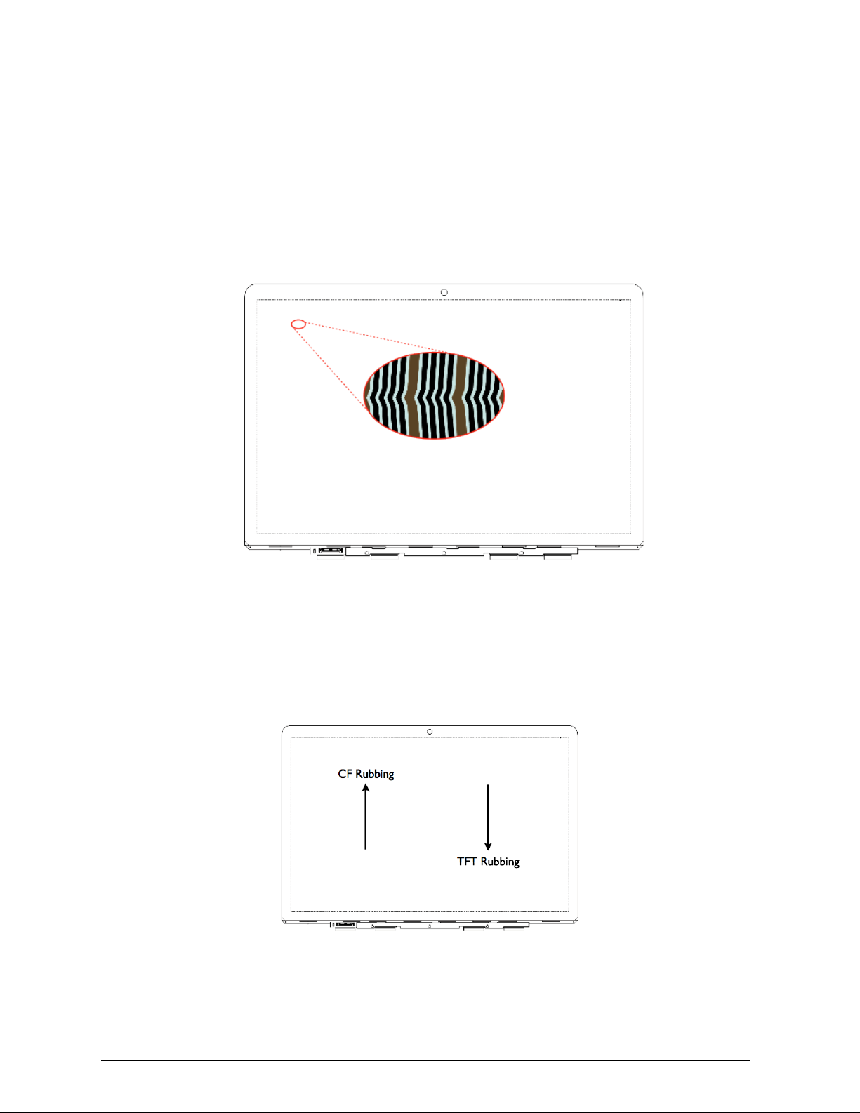
="D" 7.EE2+C',2$&*02-+'
The unit shall have Color Filter (CF) Rubbing from the bottom of the module to the top and
shall have TFT Rubbing from the top of the module to the bottom as shown in Figure 3.
Figure 3 Rubbing Directions
Page 13

THE INFORMATION CONTAINED HEREIN IS THE PROPERTY OF APPLE, INC. THE POSSESSOR AGREES TO THE FOLLOWING:
(i) TO MAINTAIN THIS DOCUMENT IN CONFIDENCE (ii) NOT TO REPRODUCE OR COPY IT (iii) NOT TO REVEAL OR PUBLISH IT IN WHOLE OR IN PART
Apple Inc.
Size: Letter
Scale: NONE
Page 13 of 67
Title: ERIS, DSPL, LCD MODULE, LGD, X34 DWG Number: 069-8326 ___Rev. B___
="F" G+0&$(1* & '1 + %',$2H2+C'I*4&/&'
The unit shall provide a 5V 4-lane DisplayPort interface, requiring Hsync and Vsync
signals, along with DE (Data Enable) mode, 1-dot Z-inversion scheme.
="J" >$-+0'I.$(1*&'K$&10/&+0'
The front surface of the unit shall provide a Dry AR1.5 coating that meets the requirements
specified herein.
D" @&*41+2*1;'7&?.2$&/&+08'
D"!" L+H&;-<&',2/&+82-+8'1+%'K-;&$1+*&8'
The unit shall meet the dimensional requirements specified in 069-7821 LCD, MCO, X34.
D"6" 3*02H&'3$&1'
The unit shall meet the active area requirement specified in 069-7821 LCD, MCO, X34.
D"9" @188'
The unit mass shall not exceed the mass specified in 069-7821 LCD, MCO, X34.
D"=" M+20'>;10+&88'
The LCD module shall meet the flatness requirement specified in 069-7821 LCD, MCO,
X34.
D"="!" >;10+&88'@&18.$&/&+0'7&?.2$&/&+08'
All units shall require a flatness measurement after aging that meet the following
requirements:
• Flatness measurement shall be completed within 24 hours after removal from
aging chamber
• Post aging, unit shall be stored in 25 +/- 3 0C and 60% +/- 5% relative humidity
D"D" LA<-8&%'3$&1'1+%'7&80$2*02-+8'
The display module shall not have exposed edges or components, which may cause injury or
damage during handling, inspection, assembly, and service. Exposed areas of the display
module (those not protected or shielded by construction) must be insulated and otherwise
protected to eliminate the possibility of electrical shorting or destructive ESD discharges
(per Section 7.2) during handling, inspection, assembly, and service.
D"F" L%C&'N.1;205'7&?.2$&/&+08'
The edge quality of the module shall be measured using an optical profiler such as the
Keyence VK-9700 or equivalent.
Page 14
THE INFORMATION CONTAINED HEREIN IS THE PROPERTY OF APPLE, INC. THE POSSESSOR AGREES TO THE FOLLOWING:
(i) TO MAINTAIN THIS DOCUMENT IN CONFIDENCE (ii) NOT TO REPRODUCE OR COPY IT (iii) NOT TO REVEAL OR PUBLISH IT IN WHOLE OR IN PART
Apple Inc.
Size: Letter
Scale: NONE
Page 14 of 67
Title: ERIS, DSPL, LCD MODULE, LGD, X34 DWG Number: 069-8326 ___Rev. B___
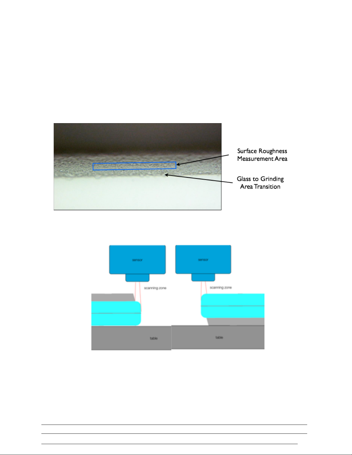
D"F"!" I.$(1*&'>2+284'7&?.2$&/&+08'
!"#"$"$" %&'()*&+&,-./&0)1*&+&,-(.
The following settings on the Keyence VK-9700 shall be used to measure the surface
finish requirements.
•
20x Objective
•
Measurement Area: 0.25 mm x 0.1 mm
•
Measurement Area distance from Glass Grinding Transition: 0.015 mm
Figure 4 Surface Roughness Measurement Area
Figure 5 Surface Roughness Measurement Test Configurations
!"#"$"2" ../33-.%&',.40)'*&.5/06.
The ground edge surface Root Mean Square shall not exceed 2.25 um.
Page 15
THE INFORMATION CONTAINED HEREIN IS THE PROPERTY OF APPLE, INC. THE POSSESSOR AGREES TO THE FOLLOWING:
(i) TO MAINTAIN THIS DOCUMENT IN CONFIDENCE (ii) NOT TO REPRODUCE OR COPY IT (iii) NOT TO REVEAL OR PUBLISH IT IN WHOLE OR IN PART
Apple Inc.
Size: Letter
Scale: NONE
Page 15 of 67
Title: ERIS, DSPL, LCD MODULE, LGD, X34 DWG Number: 069-8326 ___Rev. B___
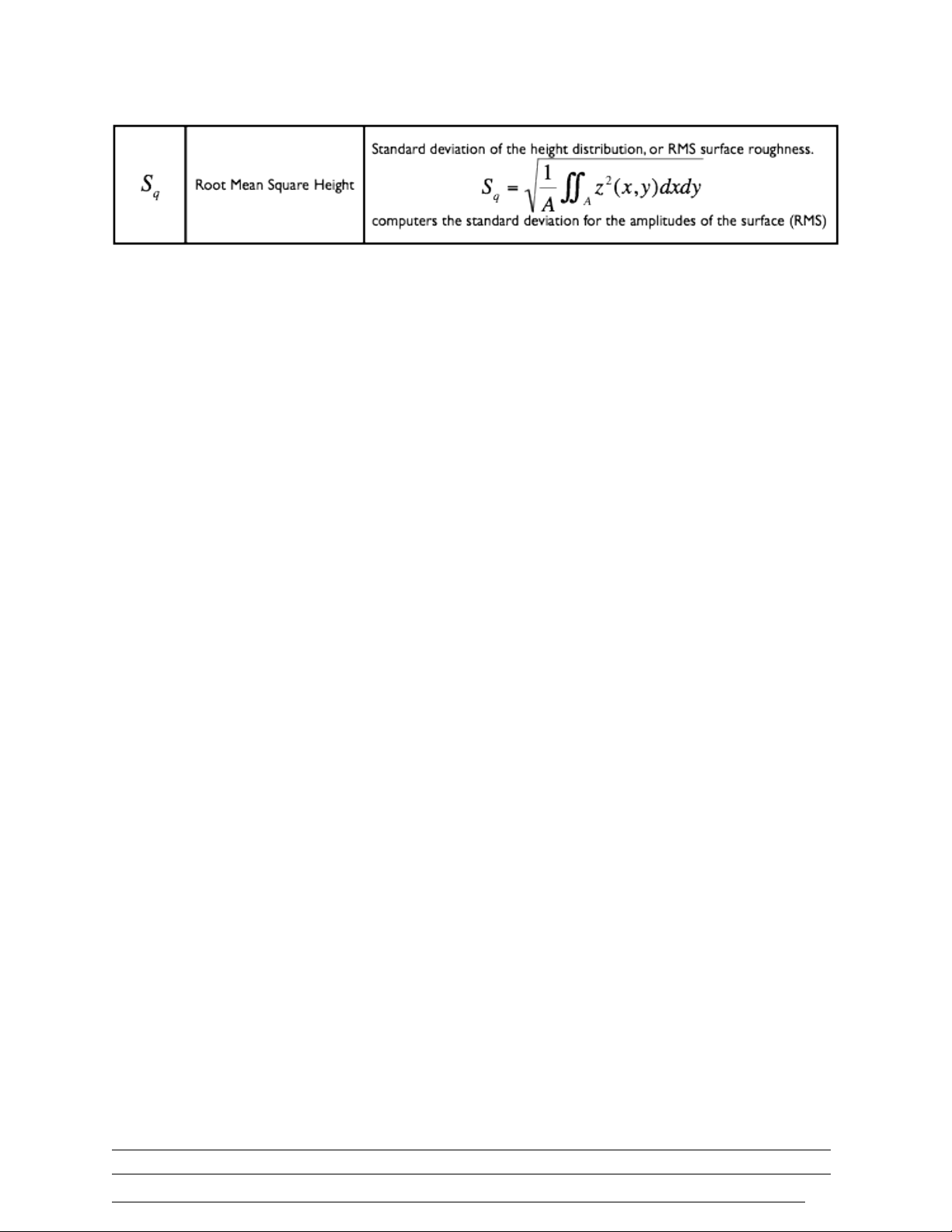
Root Mean Square is defined as:
!"#"$"7" .%'81+)+.9&1:;-.5/<=+'86.
The ground edge Maximum Height shall not exceed 25 um where maximum height is
defined as distance between the highest peak and the lowest valley.
D"F"6" 'L%C&',&(&*0'7&?.2$&/&+08'
The module shall have an edge scan completed using the Meere Company X35 EDGE
INSPECTION SYSTEM Model No. EI-AGTT-17.3.
The ground edge surface shall not exceed the following chip size requirements as
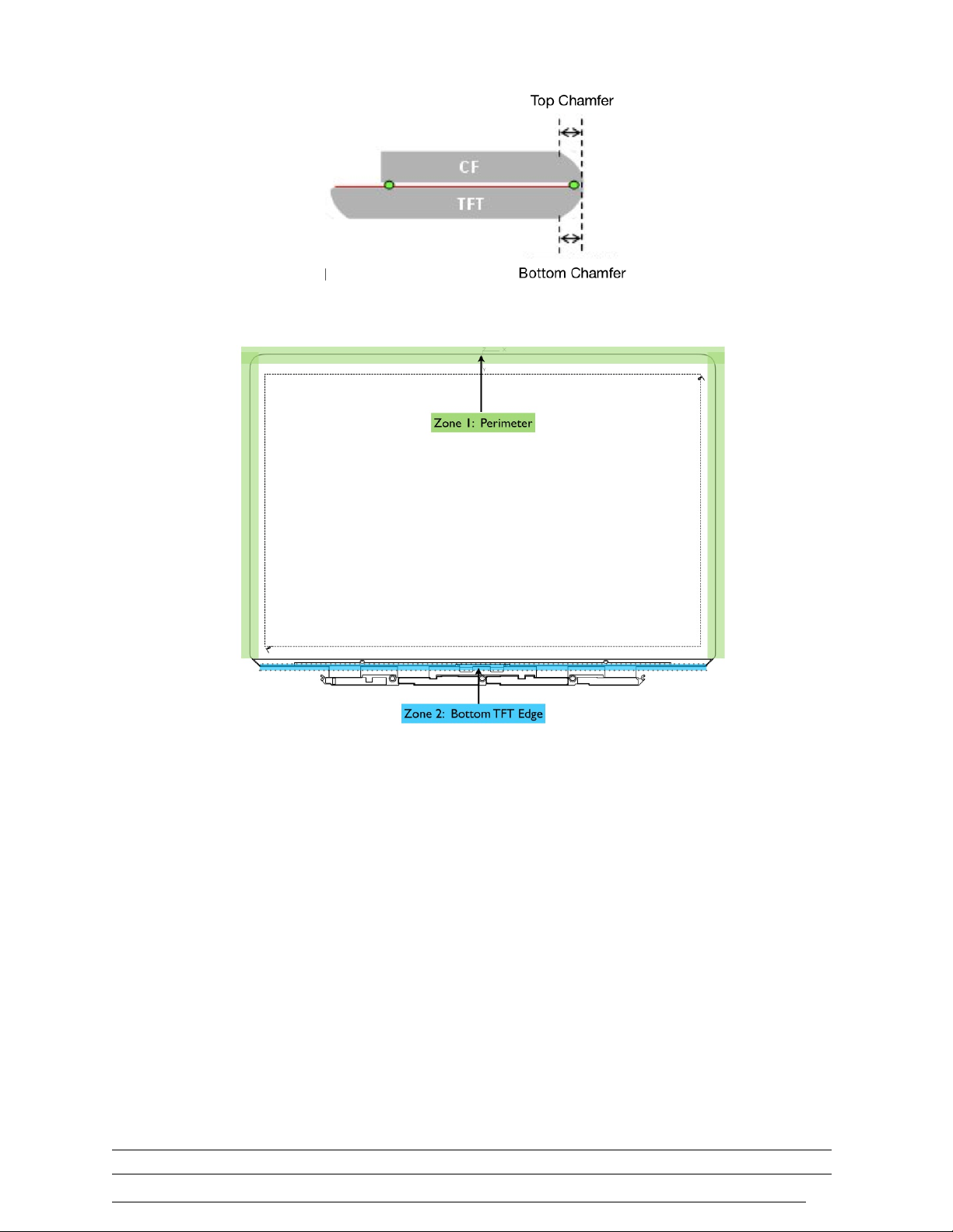
specified for each grinding zone (see Figure 6).
• Zone 1: CF/TFT Glass Perimeter (0.6t)
o 0 defects greater than 50 um in any direction
• Zone 2: Bottom TFT Ledge (0.3t)
o 0 defects greater than 50 um in any direction
• Zone 3: CF Edge (Scribe / Break)
o X-Dimension: Defect shall not exceed 500 um
o Y-Dimension: Defect shall not exceed 500 um
• Zone 4: Bottom TFT Corners (0.3t)
o X- Dimension: No defect length requirement
o Y-Dimension: Defect shall not exceed 150 um
Page 16
THE INFORMATION CONTAINED HEREIN IS THE PROPERTY OF APPLE, INC. THE POSSESSOR AGREES TO THE FOLLOWING:
(i) TO MAINTAIN THIS DOCUMENT IN CONFIDENCE (ii) NOT TO REPRODUCE OR COPY IT (iii) NOT TO REVEAL OR PUBLISH IT IN WHOLE OR IN PART
Apple Inc.
Size: Letter
Scale: NONE
Page 16 of 67
Title: ERIS, DSPL, LCD MODULE, LGD, X34 DWG Number: 069-8326 ___Rev. B___
Figure 6 Grinding Zone Definitions
Figure 7 Glass Chip Profile Definition
D"F"9" :$-.+%'I.$(1*&')$-(2;&'
The top and bottom chamfer size (Figure 8) of the glass shall meet the following
requirements shown below in the specified zone (Figure 9):
• Zone 1: CF/TFT Glass Perimeter (0.6t):
o 200 um ≥ chamfer size ≥ 60 um
• Zone 2: Bottom TFT Ledge (0.3t)
o 200 um ≥ chamfer size ≥ 50 um
X-Dimension
Y-Dimension
Glass Chip
Page 17
THE INFORMATION CONTAINED HEREIN IS THE PROPERTY OF APPLE, INC. THE POSSESSOR AGREES TO THE FOLLOWING:
(i) TO MAINTAIN THIS DOCUMENT IN CONFIDENCE (ii) NOT TO REPRODUCE OR COPY IT (iii) NOT TO REVEAL OR PUBLISH IT IN WHOLE OR IN PART
Apple Inc.
Size: Letter
Scale: NONE
Page 17 of 67
Title: ERIS, DSPL, LCD MODULE, LGD, X34 DWG Number: 069-8326 ___Rev. B___
Figure 8 Chamfer of grinding edge profile
Figure 9 Grinding Profile Zone Definitions
D"J" )-;1$2O&$'L%C&'7&?.2$&/&+0'
The laser cut polarizer edge with release lines removed shall be inspected using a variable
pressure electron microscope to evaluate polarizer edge damage.
Polarizer overhang on the edge of the polarizer caused from laser cutting shall not exceed 15
um as shown in Figure 10.
Page 18

THE INFORMATION CONTAINED HEREIN IS THE PROPERTY OF APPLE, INC. THE POSSESSOR AGREES TO THE FOLLOWING:
(i) TO MAINTAIN THIS DOCUMENT IN CONFIDENCE (ii) NOT TO REPRODUCE OR COPY IT (iii) NOT TO REVEAL OR PUBLISH IT IN WHOLE OR IN PART
Apple Inc.
Size: Letter
Scale: NONE
Page 18 of 67
Title: ERIS, DSPL, LCD MODULE, LGD, X34 DWG Number: 069-8326 ___Rev. B___
Figure 10 Polarizer Overhang Requirement
D"P" @&*41+2*1;'I01*QR.<'
The unit shall meet the stack-up requirements specified in 069-7821 LCD, MCO, X34.
Mechanical Stack-up
Part #
Nominal Thickness
(mm)
Top Polarizer
Nitto Denko NATZ-AR1.5
0.166
LCD Glass CF
-
0.30
LCD Glass TFT
-
0.30
Bottom Polarizer (glossy, APCF)
Nitto Denko APCFG3CVTT
0.162
Total
-
0.928
D"S" ,$2H&$'GB'@&*41+2*1;'7&?.2$&/&+08'
The driver IC shall meet the envelope requirements specified in 069-7821 LCD, MCO, X34.
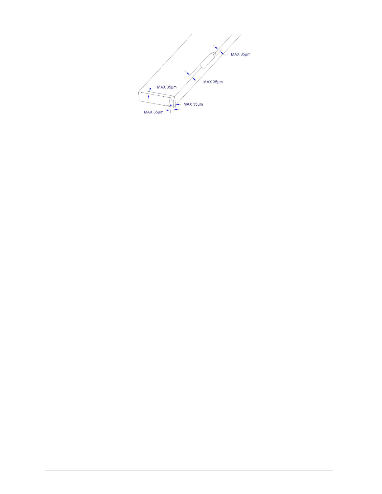
D"S"!" ',$2H&$'GB'L%C&'N.1;205'
The Driver IC chip depth shall not exceed 35 um on any edge as shown in Figure 11.
Page 19
THE INFORMATION CONTAINED HEREIN IS THE PROPERTY OF APPLE, INC. THE POSSESSOR AGREES TO THE FOLLOWING:
(i) TO MAINTAIN THIS DOCUMENT IN CONFIDENCE (ii) NOT TO REPRODUCE OR COPY IT (iii) NOT TO REVEAL OR PUBLISH IT IN WHOLE OR IN PART
Apple Inc.
Size: Letter
Scale: NONE
Page 19 of 67
Title: ERIS, DSPL, LCD MODULE, LGD, X34 DWG Number: 069-8326 ___Rev. B___
Figure 11 Driver IC Edge Quality
D"S"6" ',$2H&$'GB'K-<'I.$(1*&'7&?.2$&/&+0'
The top surface of the driver IC shall meet the following requirements as defined in
ASME B.46.1-1995
• Ra ≤ 0.015 um
• Rmax ≤ 0.100 um
D"!T" M+20'L%C&'G+Q'7&?.2$&/&+0'
A black halogen free ink approved by Apple shall be applied to the edge of the unit in the
location specified in 069-7821 LCD, MCO, X34.
F" K4&$/1;'7&?.2$&/&+08'
The unit white point color shift over temperature shall meet ∆𝑢!𝑣!≤ 0.008 from 30 °C to 50
°C.
J" L;&*0$2*1;'7&?.2$&/&+08'
The unit shall meet the electrical requirements as specified in 069-8336, X34 Display TCON
PCBA Engineering Requirements Specification (ERS), LGD.
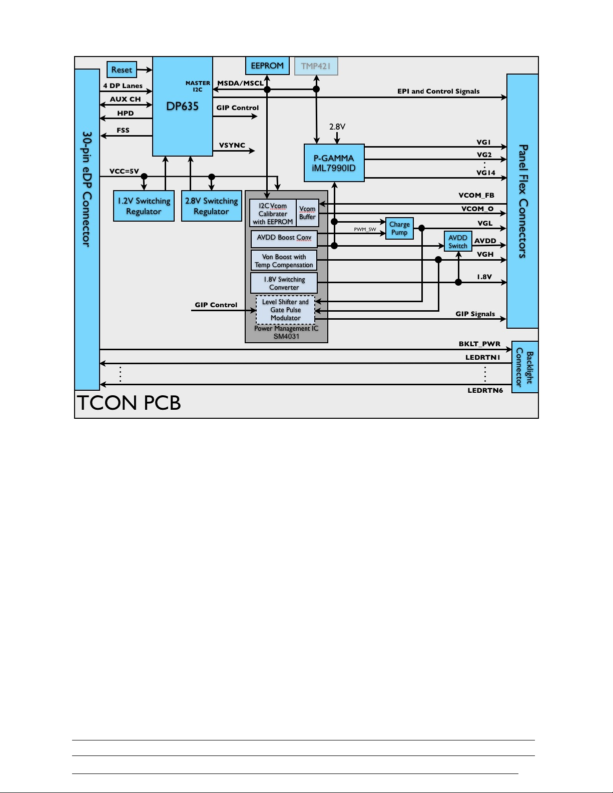
J"!" U;-*Q',21C$1/''
The unit shall meet the interface requirements as specified in 069-8336, X34 Display TCON
PCBA Engineering Requirements Specification (ERS), LGD.
The block diagram is shown in Figure 12 as reference only.
Page 20
THE INFORMATION CONTAINED HEREIN IS THE PROPERTY OF APPLE, INC. THE POSSESSOR AGREES TO THE FOLLOWING:
(i) TO MAINTAIN THIS DOCUMENT IN CONFIDENCE (ii) NOT TO REPRODUCE OR COPY IT (iii) NOT TO REVEAL OR PUBLISH IT IN WHOLE OR IN PART
Apple Inc.
Size: Letter
Scale: NONE
Page 20 of 67
Title: ERIS, DSPL, LCD MODULE, LGD, X34 DWG Number: 069-8326 ___Rev. B___
Figure 12 Unit Electrical Block Diagram (FOR REFERENCE ONLY)
J"6" ,28<;15')BU'I*4&/102*8'
The unit shall meet the schematic diagram as specified in 069-8336, X34 Display TCON
PCBA Engineering Requirements Specification (ERS), LGD.
• Schematics shall be provided with the following information:
• Numbered by version and date coding, PDF searchable
• Include signal-net page-number tags where signal-nets transfer to other pages
• Resistors to show the value, tolerance, and package information
• Capacitors to show the value, rating, tolerance, material, and package information
• Inductors to show the value, rating (current & power), tolerance, and package
information
• Fuses to show the rating and package information.
• ICs, Diodes, Inductors, Fuses, and Connectors must show the Manufacturer,
Manufacturer’s Part Number, and package information.
• Test points
Page 21
THE INFORMATION CONTAINED HEREIN IS THE PROPERTY OF APPLE, INC. THE POSSESSOR AGREES TO THE FOLLOWING:
(i) TO MAINTAIN THIS DOCUMENT IN CONFIDENCE (ii) NOT TO REPRODUCE OR COPY IT (iii) NOT TO REVEAL OR PUBLISH IT IN WHOLE OR IN PART
Apple Inc.
Size: Letter
Scale: NONE
Page 21 of 67
Title: ERIS, DSPL, LCD MODULE, LGD, X34 DWG Number: 069-8326 ___Rev. B___
J"9" ,28<;15')BU'V15-.0'
The unit shall meet PCB layout requirements specified in 069-8336, X34 Display TCON
PCBA Engineering Requirements Specification (ERS), LGD. .
The PCB CAD layout files shall be provided for Apple approval shall be an Allegro .brd file
format. The other acceptable format is Specctra format - AutoVue compatible.
J"=" 3*02H&'B-/<-+&+08'
The unit shall active components requirements as specified in 069-8336, X34 Display
TCON PCBA Engineering Requirements Specification (ERS), LGD.
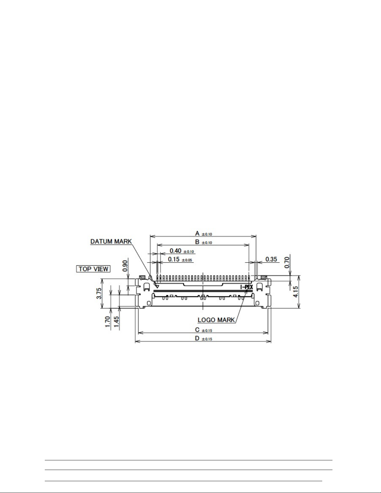
J"="!" L;&*0$2*1;'G+0&$(1*&'7&?.2$&/&+08''
>"?"$"$" @3,,&A-3*./&0)1*&+&,-(.
The unit shall provide an IPEX 20525-130E-02 connector (1.0 mm thickness, lock-in
type) as shown in Figure 13. Pin 1 on the connector is defined by the datum mark
(triangle) located on the connector (see Figure 73).
Apple will provide an IPEX 20523-130T-01 mating connector (micro-coax type).
The unit connector and mating connect shall have palladium-nickel plating (silver color).
Figure 13 Connector Drawing (PCB Side)
>"?"$"2" @3,,&A-3*.B1,.C((1:,+&,-(.
The unit shall meet connector pin assignments specified in 069-8336, X34 Display
TCON PCBA Engineering Requirements Specification (ERS), LGD.
Table 2 presents the connector pin assignments and is for reference only.
Page 22

THE INFORMATION CONTAINED HEREIN IS THE PROPERTY OF APPLE, INC. THE POSSESSOR AGREES TO THE FOLLOWING:
(i) TO MAINTAIN THIS DOCUMENT IN CONFIDENCE (ii) NOT TO REPRODUCE OR COPY IT (iii) NOT TO REVEAL OR PUBLISH IT IN WHOLE OR IN PART
Apple Inc.
Size: Letter
Scale: NONE
Page 22 of 67
Title: ERIS, DSPL, LCD MODULE, LGD, X34 DWG Number: 069-8326 ___Rev. B___
Table 2 Display Subsystem Connector Pin Assignment (FOR REFERENCE ONLY)
Pin
Signal
Description
Cable Gauge
1
BKLT_PWR
48V
Solid AWG36
2
N.C.
Arc prevention
-
3
LEDRTN6
Backlight Return Current
uCoax AWG42
4
LEDRTN5
Backlight Return Current
uCoax AWG42
5
LEDRTN4
Backlight Return Current
uCoax AWG42
6
LEDRTN3
Backlight Return Current
uCoax AWG42
7
LEDRTN2
Backlight Return Current
uCoax AWG42
8
LEDRTN1
Backlight Return Current
uCoax AWG42
9
HPD
Hot Plug
uCoax AWG42
10
FSS
Frame Sync mux
uCoax AWG42
11
AUX_P
eDP AUX
uCoax AWG42
12
AUX_N
eDP AUX
uCoax AWG42
13
GND
Shield
-
14
DP0_P
eDP pair 0
90Ω Twin-Ax AWG40
15
DP0_N
eDP Pair 0
16
GND
Shield
-
17
DP1_P
eDP pair 1
90Ω Twin-Ax AWG40
18
DP1_N
eDP pair 1
19
GND
Shield
-
20
DP2_P
eDP pair 2
90Ω Twin-Ax AWG40
21
DP2_N
eDP pair 2
22
GND
Shield
-
23
DP3_P
eDP pair 3
90Ω Twin-Ax AWG40
24
DP3_N
eDP pair 3
25
GND
Digital Ground
Solid AWG36
26
GND
Digital Ground
Solid AWG36
27
GND
Digital Ground
Solid AWG36
28
VCC
5V
Solid AWG36
29
VCC
5V
Solid AWG36
30
VCC
5V
Solid AWG36
J"="6" LA0&+%&%',28<;15'G%&+02(2*102-+',101'WL,G,X'G+0&$(1*&''
The unit shall meet EDID interface requirements specified in 069-8336, X34 Display
TCON PCBA Engineering Requirements Specification (ERS), LGD and shown in Table
3 (for reference only).
Page 23

THE INFORMATION CONTAINED HEREIN IS THE PROPERTY OF APPLE, INC. THE POSSESSOR AGREES TO THE FOLLOWING:
(i) TO MAINTAIN THIS DOCUMENT IN CONFIDENCE (ii) NOT TO REPRODUCE OR COPY IT (iii) NOT TO REVEAL OR PUBLISH IT IN WHOLE OR IN PART
Apple Inc.
Size: Letter
Scale: NONE
Page 23 of 67
Title: ERIS, DSPL, LCD MODULE, LGD, X34 DWG Number: 069-8326 ___Rev. B___
Table 3 EDID Data (FOR REFERENCE ONLY)
Field Name
#
Raw Hex
Interpretation
Header
0-7
0x00, 0xFF,
0xFF, 0xFF,
0xFF, 0xFF,
0xFF, 0x00
ID Manufacturer
Name
8-9
0x06, 0x10
APP
ID Product Code
1011
0x14, 0xA0
ID Serial Number
1215
0x00, 0x00,
0x00, 0x00
0l
Date of
Manufacture
1617
0x0A, 0x16
March 4, 2012
EDID Structure
Version/Revision
Number
1819
0x01, 0x04
1.4
Video Input
Definition
20
0xA5
Bit 7 = 1, Display accepts digital
input
Color bit depth is 8 bits per primary
color
DisplayPort is supported
Max Horizontal
Image Size
21
0x1D
29 cm
Max Vertical
Image Size
22
0x12
18 cm
Display Transfer
Characteristic
(Gamma)
23
0x78
2.20
Feature and DPMS
Support
24
0x02
Bit 7 = 0, Display doesn't support DPMS
Stand-by
Bit 6 = 0, Display doesn't support DPMS
Suspend
Bit 5 = 0, Display doesn't support DPMS
Active Off
Bits [4:3] = Supported Color Encoding
Formats, [0:0] = RGB 4:4:4 is supported
Bit 2 = 0, Display doesn't use the sRGB
standard default color space as its
primary color space
Bit 1 = 1, Display's preferred timing
is native
Bit 0 = 0, Multi-scan display
Color
Characteristics
2534
0x6F
0xB1
0xA7
0x55
0x4C
0x9E
0x25
0x0C
0x50
0x54
Red_x Value = 0.65236
Red_y Value = 0.33206
Green_x Value = 0.29692
Green_y Value = 0.61723
Blue_x Value = 0.14456
Blue_y Value = 0.04692
White_x Value = 0.31250
White_y Value = 0.32814
Established
Timing 1
35
0x00
Established
Timing 2
36
0x00
Page 24

THE INFORMATION CONTAINED HEREIN IS THE PROPERTY OF APPLE, INC. THE POSSESSOR AGREES TO THE FOLLOWING:
(i) TO MAINTAIN THIS DOCUMENT IN CONFIDENCE (ii) NOT TO REPRODUCE OR COPY IT (iii) NOT TO REVEAL OR PUBLISH IT IN WHOLE OR IN PART
Apple Inc.
Size: Letter
Scale: NONE
Page 24 of 67
Title: ERIS, DSPL, LCD MODULE, LGD, X34 DWG Number: 069-8326 ___Rev. B___
Manufacturer's
Timings
37
0x00
Standard Timing
Identification 1
3839
0x01, 0x01
not used
Standard Timing
Identification 2
4041
0x01, 0x01
not used
Standard Timing
Identification 3
4243
0x01, 0x01
not used
Standard Timing
Identification 4
4445
0x01, 0x01
not used
Standard Timing
Identification 5
4647
0x01, 0x01
not used
Standard Timing
Identification 6
4849
0x01, 0x01
not used
Standard Timing
Identification 7
5051
0x01, 0x01
not used
Standard Timing
Identification 8
5253
0x01, 0x01
not used
Detailed Timing
Description 1
5471
0xE2
0x68
0x00
0xA0
0xA0
0x40
0x2E
0x60
0x30
0x20
0x36
0x00
0x1E
0xB3
0x10
0x00
0x00
0x1A
Pixel Clock = 268.50 MHz
Horizontal Active = 2560 Pixels
Horizontal Blanking = 160 Pixels
Vertical Active = 1600 Lines
Vertical Blanking = 46 Lines
Horizontal Sync Offset (Front Porch) =
48 Pixels (from blanking start)
Horizontal Sync Pulse Width = 32 Pixels
Vertical Sync Offset = 3 lines
Vertical Sync Pulse Width = 6 Lines
Horizontal Image Size = 286 mm
Vertical Image Size = 179 mm
Horizontal Border = 0 Pixels
Vertical Border = 0 Lines
Flags:
Bit 7 = 0, Non-interlaced
Bit [6:5:0] = [0:0:x], Normal display
(non-stereo)
Bit [4:3] = [1:1], Digital Seperate
Syncs
Bit 2 = 0, negative true VSync
Bit 1 = 1, positive true HSync
Calculated Horizontal Refresh = 98.71
kHz
Calculated Vertical Refresh = 59.97 Hz
Monitor
Description 2
7289
0x00
0x00
0x00
0xFC
0x00
0x43
0x6F
0x6C
0x6F
0x72
0x20
0x4C
0x43
0x44
Monitor Name:
Color LCD
Page 25

THE INFORMATION CONTAINED HEREIN IS THE PROPERTY OF APPLE, INC. THE POSSESSOR AGREES TO THE FOLLOWING:
(i) TO MAINTAIN THIS DOCUMENT IN CONFIDENCE (ii) NOT TO REPRODUCE OR COPY IT (iii) NOT TO REVEAL OR PUBLISH IT IN WHOLE OR IN PART
Apple Inc.
Size: Letter
Scale: NONE
Page 25 of 67
Title: ERIS, DSPL, LCD MODULE, LGD, X34 DWG Number: 069-8326 ___Rev. B___
0x0A
0x20
0x20
0x20
Monitor
Description 3
90107
0x00
0x00
0x00
0x10
0x00
0x00
0x00
0x00
0x00
0x00
0x00
0x00
0x00
0x00
0x00
0x00
0x00
0x00
Dummy descriptor.
Monitor
Description 4
108
125
0x00
0x00
0x00
0x10
0x00
0x00
0x00
0x00
0x00
0x00
0x00
0x00
0x00
0x00
0x00
0x00
0x00
0x00
Dummy descriptor.
Extension Flag
126
0x00
0
Checksum
127
0x8D
141
J"="9" )-Y&$'I.<<;5'7&?.2$&/&+08'
The unit shall meet the internal power supply requirements in 069-8336, X34 Display
TCON PCBA Engineering Requirements Specification (ERS), LGD.
J"="=" I2C+1;'K2/2+C'
>"?"?"$" D+E&FF&F.G1(HI'JB3*-.5&GB6.41:,'I./&0)1*&+&,-.
The unit shall meet the digital communications interface specified in VESA DisplayPort
Standard, Version 1, Revision 1a and VESA Embedded DisplayPort Standard, Version
1.3.
Page 26

THE INFORMATION CONTAINED HEREIN IS THE PROPERTY OF APPLE, INC. THE POSSESSOR AGREES TO THE FOLLOWING:
(i) TO MAINTAIN THIS DOCUMENT IN CONFIDENCE (ii) NOT TO REPRODUCE OR COPY IT (iii) NOT TO REVEAL OR PUBLISH IT IN WHOLE OR IN PART
Apple Inc.
Size: Letter
Scale: NONE
Page 26 of 67
Title: ERIS, DSPL, LCD MODULE, LGD, X34 DWG Number: 069-8326 ___Rev. B___
>"?"?"2" G1(HI'J.K1+1,:.G'-'.
The unit shall meet display timing data requirements in 069-8336, X34 Display TCON
PCBA Engineering Requirements Specification (ERS), LGD.
>"?"?"7" @3I3*.L,H)-.G'-'./&M&*&,A&.
The color data reference specified in Table 4 shall be used for the reference for color
versus data input.
The brightness of each primary color (red, green and blue) is based on the 8-bit gray scale
data input for the color. The higher the binary input, the brighter the color.
Table 4 Color Data Reference
Input Color Data
Color
Red
MSB LSB
Green
MSB LSB
Blue
MSB LSB
R7
R6
R5
R4
R3
R2
R1
R0
G7
G6
G5
G4
G3
G2
G1
G0
B7
B6
B5
B4
B3
B2
B1
B0
Basic
Color
s
Black
Red(255)
Green(255)
Blue(255)
Cyan
Magenta
Yellow
White
0
1
0
0
0
1
1
1
0
1
0
0
0
1
1
1
0
1
0
0
0
1
1
1
0
1
0
0
0
1
1
1
0
1
0
0
0
1
1
1
0
1
0
0
0
1
1
1
0
1
0
0
0
1
1
1
0
1
0
0
0
1
1
1
0
0
1
0
1
0
1
1
0
0
1
0
1
0
1
1
0
0
1
0
1
0
1
1
0
0
1
0
1
0
1
1
0
0
1
0
1
0
1
1
0
0
1
0
1
0
1
1
0
0
1
0
1
0
1
1
0
0
1
0
1
0
1
1
0
0
0
1
1
1
0
1
0
0
0
1
1
1
0
1
0
0
0
1
1
1
0
1
0
0
0
1
1
1
0
1
0
0
0
1
1
1
0
1
0
0
0
1
1
1
0
1
0
0
0
1
1
1
0
1
0
0
0
1
1
1
0
1
Red
Red(00)
Dark
Red(01)
Red(02)
Red(253)
Red(254)
Red(255)
Bright
0
0
0
:
1
1
1
0
0
0
:
1
1
1
0
0
0
:
1
1
1
0
0
0
:
1
1
1
0
0
0
:
1
1
1
0
0
0
:
1
1
1
0
0
1
:
0
1
1
0
1
0
:
1
0
1
0
0
0
:
0
0
0
0
0
0
:
0
0
0
0
0
0
:
0
0
0
0
0
0
:
0
0
0
0
0
0
:
0
0
0
0
0
0
:
0
0
0
0
0
0
:
0
0
0
0
0
0
:
0
0
0
0
0
0
:
0
0
0
0
0
0
:
0
0
0
0
0
0
:
0
0
0
0
0
0
:
0
0
0
0
0
0
:
0
0
0
0
0
0
:
0
0
0
0
0
0
:
0
0
0
0
0
0
:
0
0
0
Gree
n
Green(00)
Dark
Green(01)
Green(02)
Green(253)
Green(254)
Green(255)
Bright
0
0
0
:
0
0
0
0
0
0
:
0
0
0
0
0
0
:
0
0
0
0
0
0
:
0
0
0
0
0
0
:
0
0
0
0
0
0
:
0
0
0
0
0
0
:
0
0
0
0
0
0
:
0
0
0
0
0
0
:
1
1
1
0
0
0
:
1
1
1
0
0
0
:
1
1
1
0
0
0
:
1
1
1
0
0
0
:
1
1
1
0
0
0
:
1
1
1
0
0
1
:
0
1
1
0
1
0
:
1
0
1
0
0
0
:
0
0
0
0
0
0
:
0
0
0
0
0
0
:
0
0
0
0
0
0
:
0
0
0
0
0
0
:
0
0
0
0
0
0
:
0
0
0
0
0
0
:
0
0
0
0
0
0
:
0
0
0
Blue
Blue(00)
Dark
Blue(01)
Blue(02)
Blue(253)
Blue(254)
Blue(255)
Bright
0
0
0
:
0
0
0
0
0
0
:
0
0
0
0
0
0
:
0
0
0
0
0
0
:
0
0
0
0
0
0
:
0
0
0
0
0
0
:
0
0
0
0
0
0
:
0
0
0
0
0
0
:
0
0
0
0
0
0
:
0
0
0
0
0
0
:
0
0
0
0
0
0
:
0
0
0
0
0
0
:
0
0
0
0
0
0
:
0
0
0
0
0
0
:
0
0
0
0
0
0
:
0
0
0
0
0
0
:
0
0
0
0
0
0
:
1
1
1
0
0
0
:
1
1
1
0
0
0
:
1
1
1
0
0
0
:
1
1
1
0
0
0
:
1
1
1
0
0
0
:
1
1
1
0
0
1
:
0
1
1
0
1
0
:
1
0
1
Page 27

THE INFORMATION CONTAINED HEREIN IS THE PROPERTY OF APPLE, INC. THE POSSESSOR AGREES TO THE FOLLOWING:
(i) TO MAINTAIN THIS DOCUMENT IN CONFIDENCE (ii) NOT TO REPRODUCE OR COPY IT (iii) NOT TO REVEAL OR PUBLISH IT IN WHOLE OR IN PART
Apple Inc.
Size: Letter
Scale: NONE
Page 27 of 67
Title: ERIS, DSPL, LCD MODULE, LGD, X34 DWG Number: 069-8326 ___Rev. B___
J"="D" )-Y&$'7&?.2$&/&+08'WZ[#'E1*Q;2C40X'
The unit (w/o backlight) shall meet the internal power requirements in 069-8336, X34
Display TCON PCBA Engineering Requirements Specification (ERS), LGD.
The unit with the backlight turned off shall meet the power requirements shown in Table
7.45 using the display pattern requirements specified in 7.4.6.
Table 7.45 Power Requirements (FOR REFERENCE ONLY)
Pattern
Nominal
Max
Unit
White
380
440
mA
Mosaic
380
440
mA
Horizontal Line -
One On / One Off
570
660
mA
Vertical Line –
One On / One Off
600
690
mA
Red
500
580
mA
Black
380
430
mA
Note: (1) Display data pins and timing signal pins should be connected (GND = 0V);
(2) Operation conditions: fV = 60 Hz, f
CLK
= 268.500 MHz, Vcc = 5 V;
J"="F" ,28<;15')100&$+'7&?.2$&/&+08'
The display patterns for system verification are defined below.
• White Pattern: All pixels in active area turned on at 100%
• Mosaic (checker) Pattern: Repeating pattern of 20 pixels x 20 pixels black an
white areas over entire active area. White area has all pixels turned on at 100%
and black area has all pixels turned off.
• Vertical Stripe Pattern: Sub-pixel vertical line alternating between power on and
power off as shown in Figure 16.
Page 28

THE INFORMATION CONTAINED HEREIN IS THE PROPERTY OF APPLE, INC. THE POSSESSOR AGREES TO THE FOLLOWING:
(i) TO MAINTAIN THIS DOCUMENT IN CONFIDENCE (ii) NOT TO REPRODUCE OR COPY IT (iii) NOT TO REVEAL OR PUBLISH IT IN WHOLE OR IN PART
Apple Inc.
Size: Letter
Scale: NONE
Page 28 of 67
Title: ERIS, DSPL, LCD MODULE, LGD, X34 DWG Number: 069-8326 ___Rev. B___
Figure 14 White Screen Display Figure 15 Mosaic Pattern Display
Figure 16 Vertical Stripe Pattern Display
J"D" )-Y&$'-+R-(('8&?.&+*&'
The unit shall meet the power on-off sequence requirements (TBD) in 069-8336, X34
Display TCON PCBA Engineering Requirements Specification (ERS), LGD.
J"F" \**'\-;01C&',$-<'7&?.2$&/&+0''
The unit shall operate as specified herein with a voltage drop (during power-on or normal
operation) specified (TBD) in 069-8336, X34 Display TCON PCBA Engineering
Requirements Specification (ERS), LGD.
J"J" ]&1$R>2&;%']-28&'
The panel vendor shall follow the noise characterization process outlined in Apple’s near
field noise spec (069-2794), and comply with noise emission limits.
Note: This spec compliance requirement is in addition to the legal EMI compliance
requirements.
J"P" &,)'U20RL$$-$R710&'WUL7X'7&?.2$&/&+0'
The unit shall meet the eDP Bit-Error rate requirements in 069-8336, X34 Display TCON
PCBA Engineering Requirements Specification (ERS), LGD.
J"S" B#:'U20'L$$-$'710&'WUL7X'7&?.2$&/&+0'
The unit COG chips shall meet the BER requirement in 069-8336, X34 Display TCON
PCBA Engineering Requirements Specification (ERS), LGD
J"!T" )$-C$1//1E;&':1//1'I&002+C8'
The programmable gamma settings for the unit are specified in 069-8336, X34 Display
TCON PCBA Engineering Requirements Specification (ERS), LGD.
Page 29

THE INFORMATION CONTAINED HEREIN IS THE PROPERTY OF APPLE, INC. THE POSSESSOR AGREES TO THE FOLLOWING:
(i) TO MAINTAIN THIS DOCUMENT IN CONFIDENCE (ii) NOT TO REPRODUCE OR COPY IT (iii) NOT TO REVEAL OR PUBLISH IT IN WHOLE OR IN PART
Apple Inc.
Size: Letter
Scale: NONE
Page 29 of 67
Title: ERIS, DSPL, LCD MODULE, LGD, X34 DWG Number: 069-8326 ___Rev. B___
J"!!" U1*Q;2C40'I.E8580&/'
J"!!"!" :&+&$1;'G+(-$/102-+'
Table 5 LED Requirements (Characterized at 20 mA)
LED Manufacturer
TG
LED Manufacturer Assembly P/N
E1S72-YW1L7-0F or Apple approved equivalent
Number of LEDs
42
LED Vf Ranks
5.3-5.5V, 5.5-5.7V
LED Forward Voltage Range for All 6
LED Series Lines
MAX: 42 V
(Characterized at Connector for 23 mA)
LED Forward Voltage Difference
between Strings
0.6V
J"!!"6" U1*Q;2C40'L;&*0$2*1;'B41$1*0&$2802*8'
>"$$"2"$" NDG.A3,-*3II&*.
The unit shall drive the LED subsystem shown in Figure 17, Figure 18, and Figure 19
Page 30

THE INFORMATION CONTAINED HEREIN IS THE PROPERTY OF APPLE, INC. THE POSSESSOR AGREES TO THE FOLLOWING:
(i) TO MAINTAIN THIS DOCUMENT IN CONFIDENCE (ii) NOT TO REPRODUCE OR COPY IT (iii) NOT TO REVEAL OR PUBLISH IT IN WHOLE OR IN PART
Apple Inc.
Size: Letter
Scale: NONE
Page 30 of 67
Title: ERIS, DSPL, LCD MODULE, LGD, X34 DWG Number: 069-8326 ___Rev. B___
Figure 17 LED Controller Block Diagram
Figure 18 LED Controller Reference Application Circuits
Page 31

THE INFORMATION CONTAINED HEREIN IS THE PROPERTY OF APPLE, INC. THE POSSESSOR AGREES TO THE FOLLOWING:
(i) TO MAINTAIN THIS DOCUMENT IN CONFIDENCE (ii) NOT TO REPRODUCE OR COPY IT (iii) NOT TO REVEAL OR PUBLISH IT IN WHOLE OR IN PART
Apple Inc.
Size: Letter
Scale: NONE
Page 31 of 67
Title: ERIS, DSPL, LCD MODULE, LGD, X34 DWG Number: 069-8326 ___Rev. B___
Figure 19 Display Backlight Control Diagram
J"!!"9" VL,'B-++&*02-+'
The display subsystem shall have a LED connection scheme as specified in Table 6.
Table 6 LED Connection Data
String
1 2 3 4 5 6 7
1
1 7 13
19
25
31
37
2
2 8 14
20
26
32
38
3
3 9 15
21
27
33
39 4 4
10
16
22
28
34
40
5
5
11
17
23
29
35
41
6
6
12
18
24
30
36
42
Table 7 LED Connector Assignments (FOR REFERENCE ONLY)
Pin
Symbol
Description
1
NC
NC
2
LEDRTN1
Backlight Return Current
3
NC
NC
4
LEDRTN2
Backlight Return Current
Page 32

THE INFORMATION CONTAINED HEREIN IS THE PROPERTY OF APPLE, INC. THE POSSESSOR AGREES TO THE FOLLOWING:
(i) TO MAINTAIN THIS DOCUMENT IN CONFIDENCE (ii) NOT TO REPRODUCE OR COPY IT (iii) NOT TO REVEAL OR PUBLISH IT IN WHOLE OR IN PART
Apple Inc.
Size: Letter
Scale: NONE
Page 32 of 67
Title: ERIS, DSPL, LCD MODULE, LGD, X34 DWG Number: 069-8326 ___Rev. B___
5
NC
NC
6
LEDRTN3
Backlight Return Current
7
NC
NC
8
LEDRTN4
Backlight Return Current
9
BKLT_PWR
Backlight Power (48V)
10
LEDRTN5
Backlight Return Current
11
BKLT_PWR
Backlight Power (48V)
12
LEDRTN6
Backlight Return Current
J"!!"=" VL,'80$2+C'0-'80$2+C'*.$$&+0'H1$2102-+'
LED current variation from string to string is defined as ⊗ = (I
max
- I
min
)/I
avg,
where I
max
and I
min
are the maximum and minimum current on any of the 6 strings, respectively.
LED current variation ⊗ should be within ±2.0% during the complete range of PWM
dimming from 20mA (100% duty) to 0.4mA (2% duty)
J"!!"D" VL,',$2H&$'7&?.2$&/&+0'
16-bit dimming control through Pulse Width Modulation (PWM) scheme with consistent
current on LED strings. The LED string PWM signal frequency is 8KHz or higher.
Between each string a 60 degree phase delay is implemented.
J"!6" 'GK#'L;&*0$2*1;'I42&;%2+C'
A transparent ITO layer shall be applied on the top surface of the CF Glass for electrical
shielding that meet the electrical requirements specified in Table 8 and Figure 20.
Table 8 ITO Layer Characteristics
Minimum
Typical
Maximum
ITO Sheet Resistance
-
2000 Ω/square
2500 Ω/square
Grounding Method
Black conductive tape connecting ITO on Color Filter Surface to ground
Module level ITO
transmittance (with polarizer)
98%
99%
-
Module level ITO white point
shift (delta x & delta y)
- - 0.001
Page 33

THE INFORMATION CONTAINED HEREIN IS THE PROPERTY OF APPLE, INC. THE POSSESSOR AGREES TO THE FOLLOWING:
(i) TO MAINTAIN THIS DOCUMENT IN CONFIDENCE (ii) NOT TO REPRODUCE OR COPY IT (iii) NOT TO REVEAL OR PUBLISH IT IN WHOLE OR IN PART
Apple Inc.
Size: Letter
Scale: NONE
Page 33 of 67
Title: ERIS, DSPL, LCD MODULE, LGD, X34 DWG Number: 069-8326 ___Rev. B___
Figure 20 ITO Transmittance
Glass
Glass
Tr (1) %
Tr (2) %
Tr% = Tr(2) /Tr(1)
Page 34

THE INFORMATION CONTAINED HEREIN IS THE PROPERTY OF APPLE, INC. THE POSSESSOR AGREES TO THE FOLLOWING:
(i) TO MAINTAIN THIS DOCUMENT IN CONFIDENCE (ii) NOT TO REPRODUCE OR COPY IT (iii) NOT TO REVEAL OR PUBLISH IT IN WHOLE OR IN PART
Apple Inc.
Size: Letter
Scale: NONE
Page 34 of 67
Title: ERIS, DSPL, LCD MODULE, LGD, X34 DWG Number: 069-8326 ___Rev. B___
P" #<02*1;'7&?.2$&/&+08' '
P"!" :&+&$1;'#<02*1;'I<&*2(2*102-+8'
The optical performance will be approved by Apple based on supplier’s measurement data,
visual inspection of the samples, verification measurements, and specification correlation.
Table 9 General Optical Characteristics
Parameter
Symbol
Condition
Min.
Typ.
Max.
Unit
Note
Spec
Iso-Contrast
Viewing Angle
$
CR ≥ 100
Horizontal and
Vertical
Directions
75
85
-- ° 1,2,3
8.15
CR ≥ 10
Horizontal and
Vertical
Directions
85
89
°
CR ≥ 100
@ any other
angle
35
40
--
°
No Gray Inversion
Angle
$
Any Angle
90 - -- ° 1,2,3
8.16
Contrast ratio
CR
Optimal
750
900
--
--
1,2,3
8.7
Color Shift
du’v’
White (255/255)
--
--
0.02
--
1,2,3
du’v’
Gray (127/255)
--
--
0.03
--
1,2,3
Transmittance
T
with standard
BLU
3.75
4.0
-- % 1,2,4,5
White Chromaticity
Wx
CIE 1931
0.298
0.313
0.328
--
1,2,3,5
8.14
Wy
0.314
0.329
0.344
--
1,2,3,5
Red Chromaticity
Rx
CIE 1931
0.625
0.640
0.655
--
1,2,3,5
Ry
0.320
0.330
0.340
--
1,2,3,5
Green Chromaticity
Gx
CIE 1931
0.285
0.300
0.315
--
1,2,3,5
Gy
0.580
0.600
0.620
--
1,2,3,5
Blue Chromaticity
Bx
CIE 1931
0.140
0.150
0.160
--
1,2,3,5
By
0.050
0.060
0.070
--
1,2,3,5
Black Chromaticity
No visible hue
on black screen
Blue Shift Over
Temperature
∆u’v’
30 °C to 50 °C
0.008
1,2,3,5
Max color
difference over a
cell
du’v’
white
--
--
0.0055
--
1,2
8.11
Max color
difference w.r.t.
Center
du’v’
white
--
--
0.0045
--
1,2
8.10
Page 35

THE INFORMATION CONTAINED HEREIN IS THE PROPERTY OF APPLE, INC. THE POSSESSOR AGREES TO THE FOLLOWING:
(i) TO MAINTAIN THIS DOCUMENT IN CONFIDENCE (ii) NOT TO REPRODUCE OR COPY IT (iii) NOT TO REVEAL OR PUBLISH IT IN WHOLE OR IN PART
Apple Inc.
Size: Letter
Scale: NONE
Page 35 of 67
Title: ERIS, DSPL, LCD MODULE, LGD, X34 DWG Number: 069-8326 ___Rev. B___
Parameter
Symbol
Condition
Min.
Typ.
Max.
Unit
Note
Spec
Max color
difference between
neighbors
du’v’
white
--
--
0.0022
--
1,2
8.13
Gamma
--
--
2.25
--
--
1,2,3
Flicker
F
No Visual
Flicker
--
--
-60
dB
1,2,3
8.21
Cross Talk
DSHA
No Visible
cross-talk
--
--
1.0 % 1,2,3
8.22
Response (rise +
fall time)
& on+off
$ = 0°,
Ta=30°C
--
20
30
ms
1,2,3
8.17
Gray to Gray
Response time
& G2G
$ = 0°,
Ta=30°C
--
17
20
ms
1,2,3
8.19
Surface Reflection
R
D65 Light
1.7
1.85
% 8.6
AA Reflection
Color
a*
D65 Light
-2
1
4
b*
5
8.5
12
Note 1: The testing conditions are specified in 6.2.
Note 2: The definitions of optical characteristics are shown in 6.3.
Note 3: Measured at center point. Equivalent performance over the entire panel required.
Note 4: Both center point and average of 160 points.
Note 5: Test with standard BLU.
Note 6: Color measurements shall meet CpK 1.0
Note 7: Color uniformity measurement shall be done with single point light source (see Sec. 8.2.5)
P"6" #<02*1;'@&18.$2+C'B-+%202-+8'
The optical characteristics are determined after the unit has been done with aging chamber at
the maximum brightness, in a dark environment at an ambient temperature at 25°C ± 2°C.
The electrical conditions include Vcc = 5.0 V, fv = 60 Hz, f
CLK
= 268.50 MHz, I
LED
= 23.0
mA at 100% duty cycle. Recommended measuring equipment for luminance and color is
Photo Research PR650 Colorimeter or similar. The measuring distance should be about 150
cm from the LCD surface at normal unless otherwise specified. The (virtual) measuring spot
should be 5mm in diameter. The CIE 1931 and 1967 Standards shall be used. Measurements
should be done on the 160 grid points as shown in the following figures. Viewing angle
measurements should be done by an Eldim EZ Color system or similar. Measurement data
needs to be calibrated to Apple’s equipment measurement results.
Page 36

THE INFORMATION CONTAINED HEREIN IS THE PROPERTY OF APPLE, INC. THE POSSESSOR AGREES TO THE FOLLOWING:
(i) TO MAINTAIN THIS DOCUMENT IN CONFIDENCE (ii) NOT TO REPRODUCE OR COPY IT (iii) NOT TO REVEAL OR PUBLISH IT IN WHOLE OR IN PART
Apple Inc.
Size: Letter
Scale: NONE
Page 36 of 67
Title: ERIS, DSPL, LCD MODULE, LGD, X34 DWG Number: 069-8326 ___Rev. B___
Figure 21 Optical Measurement Set-up
Figure 22 Optical Measurement Points
P"6"!" B&+0&$')-2+0'V./2+1+*&'
Lct = Average luminance at point #72, 73, 88, 89 point of the display
Page 37

THE INFORMATION CONTAINED HEREIN IS THE PROPERTY OF APPLE, INC. THE POSSESSOR AGREES TO THE FOLLOWING:
(i) TO MAINTAIN THIS DOCUMENT IN CONFIDENCE (ii) NOT TO REPRODUCE OR COPY IT (iii) NOT TO REVEAL OR PUBLISH IT IN WHOLE OR IN PART
Apple Inc.
Size: Letter
Scale: NONE
Page 37 of 67
Title: ERIS, DSPL, LCD MODULE, LGD, X34 DWG Number: 069-8326 ___Rev. B___
P"6"6" 3H&$1C&'V./2+1+*&'
L
Ave
= SUM(L1:L
160
) / 160
where L1 to L
160
are the luminance values measured at point #1 to #160.
P"6"9" U$2C40+&88'M+2(-$/205''
No visible brighter or darker bandings, or any kind of shapes objects on the screen will be
allowed. Apple requires two kinds of data for brightness uniformity: Luminance
Uniformity, and Worst Neighbor Luminance Uniformity. The definitions are shown in
below:
Global Luminance Uniformity:
• UL = 100% - (L
max-Lmin
)/L
max
• L
max
= max {Luminance values at 160 points},
• L
min
= min {Luminance values at 160 points}
• Worst Neighbor Luminance Uniformity (The 4 points that are closest to the test
point)
• WNUL=100%-Max(⊗L1, ⊗L2, ⊗L3, ⊗L4)/L0
• Global WNU = min (WNU1, …WNU160)
Figure 23 Neighboring points
P"6"=" B-+0$180'7102-''
CR = Luminance at White / Luminance at Black.
P"6"D" Z420&'B-;-$'M+2(-$/205''
The entire display active area shall be scanned with the color coordinate measurement
with white screen set full brightness. A point light source with standard backlight can be
prepared. The color uniformity of whole cell shall be measured with scanning method on
the point light source.
Page 38

THE INFORMATION CONTAINED HEREIN IS THE PROPERTY OF APPLE, INC. THE POSSESSOR AGREES TO THE FOLLOWING:
(i) TO MAINTAIN THIS DOCUMENT IN CONFIDENCE (ii) NOT TO REPRODUCE OR COPY IT (iii) NOT TO REVEAL OR PUBLISH IT IN WHOLE OR IN PART
Apple Inc.
Size: Letter
Scale: NONE
Page 38 of 67
Title: ERIS, DSPL, LCD MODULE, LGD, X34 DWG Number: 069-8326 ___Rev. B___
P"6"F" )1+&;'0-')1+&;'Z420&'B-;-$'M+2(-$/205''
The center point (as defined by the average value at point #72, 73, 88, 89) white color
coordinate of any panel shall be within the box with 4 corners coordination boundary
listed in Table 6.1.
P"6"J" @1A'B-;-$',2((&$&+*&'Y204'$&8<&*0'0-'04&'*&+0&$'Y2042+'1'<1+&;'
On each panel, the maximum color difference between any of the 160 points and the
center point (defined as the average value at point #72, 73, 88, 89), represented in delta
u’v’.
P"6"P" @1A'B-;-$',2((&$&+*&'E&0Y&&+'1+5'0Y-'<-2+08'Y2042+'04&'<1+&;'
On each panel, the maximum color difference between any two of the 160 points,
represented in delta u’v’.
P"6"S" 3H&$1C&'B-;-$',2((&$&+*&'E&0Y&&+'0-<'1+%'E-00-/'
On each backlight, the average color difference between top and bottom is calculated as
select a white LED backlight with good luminance and color
uniformity (>80% in luminance and <0.005 overall color).
20 mm x 20 mm
Page 39

THE INFORMATION CONTAINED HEREIN IS THE PROPERTY OF APPLE, INC. THE POSSESSOR AGREES TO THE FOLLOWING:
(i) TO MAINTAIN THIS DOCUMENT IN CONFIDENCE (ii) NOT TO REPRODUCE OR COPY IT (iii) NOT TO REVEAL OR PUBLISH IT IN WHOLE OR IN PART
Apple Inc.
Size: Letter
Scale: NONE
Page 39 of 67
Title: ERIS, DSPL, LCD MODULE, LGD, X34 DWG Number: 069-8326 ___Rev. B___
P"6"!T" @1A'B-;-$',2((&$&+*&'E&0Y&&+'0Y-'+&2C4E-$8'
On each panel, the maximum color difference between any two neighboring points on the
panel, represented in delta u’v’
P"6"!!" 7:U'B-;-$'B4$-/102*205'
The entire display active area shall be scanned with the color coordinate measurement
with screen set to full brightness and solid R, G, B color respectively. The measured color
coordinate of any panel shall be within the box with 4 corners coordination boundary
listed in Table 6.1.
P"6"!6" \2&Y2+C'3+C;&''
The viewing angle is defined as the viewing angle range under the condition at CR >
10:1.
Figure 24 Viewing angle definition
P"6"!9" :$15'I*1;&'G+H&$82-+'
Luminance vs. viewing angle curves are measured based on gray level 255, 223, 191,
159, 127, 95, 63, 32 and 0, in the viewing angle of left, right, up, down, with PCB on the
bottom side. Gray scale inversion happens when a higher gray scale measures the same
luminance or lower luminance than any of the lower gray scale.
Page 40

THE INFORMATION CONTAINED HEREIN IS THE PROPERTY OF APPLE, INC. THE POSSESSOR AGREES TO THE FOLLOWING:
(i) TO MAINTAIN THIS DOCUMENT IN CONFIDENCE (ii) NOT TO REPRODUCE OR COPY IT (iii) NOT TO REVEAL OR PUBLISH IT IN WHOLE OR IN PART
Apple Inc.
Size: Letter
Scale: NONE
Page 40 of 67
Title: ERIS, DSPL, LCD MODULE, LGD, X34 DWG Number: 069-8326 ___Rev. B___
P"6"!=" 7&8<-+8&'K2/&'
O"2"$?"$" P,.',F.PMM./&(H3,(&.K1+&.
The On/Off response time, tR + tF, is defined in the following figure and shall be
measured by switching the input signal for “black” and “white”.
Figure 25 Response Time Measurement
O"2"$?"2" Q*'J.-3.Q*'J./&(H3,(&.K1+&.
Gray to Gray Response Time is measured in a similar method. But instead of switching
display between black and white, panel is switched between two gray scales. The
maximum gray-to-gray response time is based on 9 levels of gray scales. The 9 levels are:
gray level 255, 223, 191, 159, 127, 95, 63, 32 and 0. Figure 6-6 shows an example of
Gray to Gray Response Time measurement data.
Page 41

THE INFORMATION CONTAINED HEREIN IS THE PROPERTY OF APPLE, INC. THE POSSESSOR AGREES TO THE FOLLOWING:
(i) TO MAINTAIN THIS DOCUMENT IN CONFIDENCE (ii) NOT TO REPRODUCE OR COPY IT (iii) NOT TO REVEAL OR PUBLISH IT IN WHOLE OR IN PART
Apple Inc.
Size: Letter
Scale: NONE
Page 41 of 67
Title: ERIS, DSPL, LCD MODULE, LGD, X34 DWG Number: 069-8326 ___Rev. B___
Figure 26 Gray to Gray Response Time
P"6"!D" :$15'I*1;&'V2+&1$205'-$':1//1'\1;.&'
The display luminance, LG, is measured at the different gray scales, G
min
, …, G
max
. The
exponential fitting is used to determine the gamma () value, which should be an
intrinsic or uncorrected characteristic.
LG ~ Gϒ.
P"9" >;2*Q&$'
The unit shall not have any visual flicker and shall not exceed -60 dB as calculated from the
following equation.
F = 10 Log (Px / P0).
The flicker level should be measured with gray level patterns. The output signal of a
photometer is sent to an FFT analyzer. The flicker is a ratio of the powers in the frequency
spectrum at 30 Hz (Px) and 0 Hz (P0), i.e.,
P"=" B$-88R01;Q'
The unit shall not have any visual cross talk. Cross-talk, D
SHA
, is defined by the following
equation.
DSHA = (LB – LA)/LB • 100%,
LA = Luminance in Pattern A
Page 42

THE INFORMATION CONTAINED HEREIN IS THE PROPERTY OF APPLE, INC. THE POSSESSOR AGREES TO THE FOLLOWING:
(i) TO MAINTAIN THIS DOCUMENT IN CONFIDENCE (ii) NOT TO REPRODUCE OR COPY IT (iii) NOT TO REVEAL OR PUBLISH IT IN WHOLE OR IN PART
Apple Inc.
Size: Letter
Scale: NONE
Page 42 of 67
Title: ERIS, DSPL, LCD MODULE, LGD, X34 DWG Number: 069-8326 ___Rev. B___
LB = Luminance in Pattern B.
Two luminance values are measured at center spot with 50 x 50 pixels.
Figure 27 Cross Talk Measurement
P"D" I.$(1*&'7&(;&*02-+'
Surface reflection measurement shall be measured with D65 light source and the incident
angle is 10°. The measurement setup is illustrated in Figure 88. The LCD is with proper ITO
coating and front polarizer laminated. Both black matrix and active area are needed to be
characterized.
Page 43

THE INFORMATION CONTAINED HEREIN IS THE PROPERTY OF APPLE, INC. THE POSSESSOR AGREES TO THE FOLLOWING:
(i) TO MAINTAIN THIS DOCUMENT IN CONFIDENCE (ii) NOT TO REPRODUCE OR COPY IT (iii) NOT TO REVEAL OR PUBLISH IT IN WHOLE OR IN PART
Apple Inc.
Size: Letter
Scale: NONE
Page 43 of 67
Title: ERIS, DSPL, LCD MODULE, LGD, X34 DWG Number: 069-8326 ___Rev. B___
Figure 28 Surface Reflection Measurement
P"F" :&+&$1;'7&?.2$&/&+0'(-$'B1/&$1'1+%'BGV[3VI'3$&1'
Table 10 Camera and CIL/ALS Requirements
Spec Item
Value
Note
Camera
Window
Transmittance
4.0dB±0.1dB
Parallelism
<25 arc seconds
Transmitted wavefront
OPD<λ/2
Water/oil mark and stain
Not allowed
Total dig, scratch, dust and
white spots
<20 um
Air bubbles
Not allowed
Haze
0.3% max
Color shift (Typ., transmitted)
a*
-1.8
Color shift (Typ., transmitted)
b*
4.5
Color shift max variation ∆a*
0.5
Color shift max variation ∆b*
0.5
ALS
Transmittance
16.8dB±0.1dB
CIL
Transmittance
15.2dB±0.1dB
Page 44

THE INFORMATION CONTAINED HEREIN IS THE PROPERTY OF APPLE, INC. THE POSSESSOR AGREES TO THE FOLLOWING:
(i) TO MAINTAIN THIS DOCUMENT IN CONFIDENCE (ii) NOT TO REPRODUCE OR COPY IT (iii) NOT TO REVEAL OR PUBLISH IT IN WHOLE OR IN PART
Apple Inc.
Size: Letter
Scale: NONE
Page 44 of 67
Title: ERIS, DSPL, LCD MODULE, LGD, X34 DWG Number: 069-8326 ___Rev. B___
'
P"J" B1/&$1[3VI[BGV'#<02*1;')1$1/&0&$',&(2+202-+'
P"J"!" 'B1/&$1'Z2+%-Y'K$1+8/2001+*&''
Camera window transmittance is the fraction of light transmittance through window area.
The LCD shall be with proper ITO thicker coated and front polarizer laminated. The light
source is D65 white light.
P"J"6" 'B1/&$1'Z2+%-Y')1$1;;&;28/'
Parallelism is also called wedge, which is a measure of how parallel are the polarizer
surface vs rear TFT glass surface. It can be determined by interferometry of polarizer
reflected and TFT glass reflected wavefront.
P"J"9" 'B1/&$1'Z2+%-Y'K$1+8/200&%'Z1H&($-+0',280-$02-+'
Transmitted wavefront distortion (TWD) is a measure of phase distortion, which usually
influenced by surface roughness and inhomogeneous refractive index of optical medium.
TWD shall be measured with a He-Ne laser (λ=632.8 nm) interferometer associated with
a reference plane with distortion less than λ/20. The transmitted wavefront and reflected
wavefront from reference plane is combined into interferometer. The fringe pattern from
interferometry is used to determine the TWD. One fringe is correspondent to one half
wavelength distortion.
P"J"=" '^1O&'
Haze is a measure of light scattering by an inhomogeneous medium. It can be measured
by BYK haze-gard plus or equivalent.
P"J"D" 'B-;-$'I42(0'
Color shift is determined with D65 light source and the color shift is measured with
L*a*b* standard.
P"J"F" '3VI'1+%'BGV'K$1+8/2001+*&'
ALS and CIL transmittance shall be measured by X-Rite OD meter. Since the collection
lens and illumination area of OD meter is larger than the diameter of ALS and CIL
pattern. A 0.8 mm thick steel plate with 1.6 mm opening has to be used for calibration.
The measurement method and principle are illustrated in Figure 89. The transmittance of
ALS and CIL pattern can be calculated by the OD value measured
• ODALS=log(I1/I2)=OD2-OD1
• ODCIL=log(1.2x1.2/1.6x1.6)+log(I1/I2)=OD2-OD1-2.5dB
Page 45

THE INFORMATION CONTAINED HEREIN IS THE PROPERTY OF APPLE, INC. THE POSSESSOR AGREES TO THE FOLLOWING:
(i) TO MAINTAIN THIS DOCUMENT IN CONFIDENCE (ii) NOT TO REPRODUCE OR COPY IT (iii) NOT TO REVEAL OR PUBLISH IT IN WHOLE OR IN PART
Apple Inc.
Size: Letter
Scale: NONE
Page 45 of 67
Title: ERIS, DSPL, LCD MODULE, LGD, X34 DWG Number: 069-8326 ___Rev. B___
Figure 29 Camera/ALS/CIL pattern measurement
P"P" G/1C& '7&0&+02-+'
The unit shall meet the quick check, short term, middle term, and long term image retention
requirements specified below.
The image retention test should be conducted with ~500 lux ambient illumination, 30-50cm
viewing distance, at 90 degree viewing angle. Test should be conducted at 45°C, with
23mA, 5mA, and 0.4mA LED current, or equivalent PWM duty cycle.
Figure 30 Image Retention Checking Condition
1.6 mm
ALS Calibration Fixture
X-Rite OD Meter
Zero out, OD0=0
Get OD1=log(I0/I1)
Get OD2=log(I0/I2)
Page 46

THE INFORMATION CONTAINED HEREIN IS THE PROPERTY OF APPLE, INC. THE POSSESSOR AGREES TO THE FOLLOWING:
(i) TO MAINTAIN THIS DOCUMENT IN CONFIDENCE (ii) NOT TO REPRODUCE OR COPY IT (iii) NOT TO REVEAL OR PUBLISH IT IN WHOLE OR IN PART
Apple Inc.
Size: Letter
Scale: NONE
Page 46 of 67
Title: ERIS, DSPL, LCD MODULE, LGD, X34 DWG Number: 069-8326 ___Rev. B___
Figure 31 Image Retention Checking Patterns
P"P"!" N.2*Q'B4&*Q'G/1C&'7&0&+02-+'
The residual pattern on the unit shall disappear in < 1 second on a uniform background of
a gray scale 31.
The unit shall start from 30°C and immediately after turning on the unit display the
checker pattern for 10 seconds.
P"P"6" I4-$0'K&$/'G/1C&'7&0&+02-+'
The residual pattern on the unit shall disappear in < 1 minutes on a uniform background
of a gray scale 31.
The unit shall start from 30°C and immediately after turning on the unit display the
checker pattern for 3 minutes.
P"P"9" @2%%;&'K&$/'
The residual pattern on the unit shall disappear in < 10 seconds on a uniform background
of a gray scale 127.
The unit shall start from 30°C and immediately after turning on the unit display the
checker pattern for 60 minutes.
P"P"=" V-+C'K&$/'
The residual pattern on the unit shall disappear in < 10 minutes on a uniform background
of a gray scale 127.
The unit shall start from 30°C and immediately after turning on the unit display the
checker pattern for 6 hours.
P"S" B-//-+'\-;01C&'W\*-/X'K.+2+C'7&?.2$&/&+08'
The module Vcom level shall be tuned using the following requirements to meet the image
retention requirements specified in Section 8.8.
Big Checker
Gray Scale 127 Gray Scale 31
Page 47

THE INFORMATION CONTAINED HEREIN IS THE PROPERTY OF APPLE, INC. THE POSSESSOR AGREES TO THE FOLLOWING:
(i) TO MAINTAIN THIS DOCUMENT IN CONFIDENCE (ii) NOT TO REPRODUCE OR COPY IT (iii) NOT TO REVEAL OR PUBLISH IT IN WHOLE OR IN PART
Apple Inc.
Size: Letter
Scale: NONE
Page 47 of 67
Title: ERIS, DSPL, LCD MODULE, LGD, X34 DWG Number: 069-8326 ___Rev. B___
The optimized Vcom setting is defined as the Vcom value obtained by minimizing the
flicker level using flicker meter CA210 or equivalent.
Vcom Tuning Requirements:
• Center Vcom setting shall have a -2 steps offset based on image retention margin.
• Vcom tuning accuracy shall be within ±4 steps with respect to center Vcom setting.
• To avoid transient flicker effect, panel shall be warmed up at least 1 min before
doing Vcom tuning. Longer dwell time can be applied as needed.
P"!T" B-;-$'Z184-.0'
P"!T"!" 'K&802+C'@&04-%'1+%'B-+%202-+'
The cell shall be installed with Apple designed backlight fixture and the unit shall be
‘ON’ and stable at the maximum brightness, in a dark environment with no ambient light,
and temperature at 25°C ± 2°C. The electrical conditions include Vcc = 5.0 V, fv = 60
Hz, fCLK = 268.50 MHz, ILED = 23.0 mA at 100% duty cycle. A force is applied on the
cell at the location specified in Figure 32 and details of condition are listed in Table 11.
Figure 32 Color Washout Test Locations
Table 11 Color Washout Test Conditions
Parameter
Specification
Down speed
1000 mm/min
R
S
337.36
3
2
1
REV
DESCRIPTION
OF
REVISION
ECO#
01
INITIAL
RELEASE
ERIC_LU
08/11/11
03
UPDATE
DIMENSIONS,
REVISE
UV
SEAL
PATH,
ADD
FAI,
MOVE
COG
SALVADOR
08/23/11
04 0001267214
UPDATED
DIMENSIONS,
ADDED
FAI-123,
REMOVED
HOLE
IN
THE
FRONT
POLARIZER,
UPDATE
COG
SPACER
THICKNESS,
UPDATE
ITO
TAPE
SHAPE
AND
THICKNESS,
REVISE
TOLERANCE
ON
FAI
27,79,81,;
REMOVE
LIQUID
CRYSTAL
SEAL
PATH
OPTION
SALVADOR
09/20/11
05 0001283842
REVISE
NOTES
19,20,21;ADD
SPC;
CORRECT
FAI
20
TOL.
SHT
2;
CORRECT
NOTE
22
LEADERS,
SHT
3;
UPDATE
DIMS
OF
COG
SPACER,
DELETE
EXTRANEOUS
DIMS
AND
FAI,ADD
SECTION
AK-AK,
SHT
5;
UPDATE
FLATNESS
PTS
AND
CALCS,
SHT
6;
UPDATE
FLATNESS
FIXTURE,
SHT
7;
REVISE
DETAIL
P,
SHT
9
SALVADOR
11/01/11
06 0001295788
CORRECT
APN
TYPO
NOTE
21;ADD
ITO
TAPE
AND
COG
AS
SEPARATE
ITEMS;
REVISE
NOTE
FOR
BM
IN
DETAIL
AJ,
SHT
4
SALVADOR
11/11/11
07 0001373136
ADD
VENDOR
CAD FOR
REFERENCE,
REVISE
TOLERANCE
ON
FAI
77;FAI
85
ADD
NOTE
TO
FEATURE
CONTROL
FRAME,
DELETE
NOTE
18,ADD
FAI
131-136,
REVISE
DIMENSION
AND
TOLERANCE
FOR
FAI
81,
REVISE
COG
SPACER
POSITION
AND
GEOMETRY,
ADD
SHT
10
AND
REAR
POL
TABS,
UPDATE
SECTION
AF-AF
TO
ADD
TUFFY
ADHESIVE
DIM
AND
FAI
SALVADOR
12/13/11
Page 48

THE INFORMATION CONTAINED HEREIN IS THE PROPERTY OF APPLE, INC. THE POSSESSOR AGREES TO THE FOLLOWING:
(i) TO MAINTAIN THIS DOCUMENT IN CONFIDENCE (ii) NOT TO REPRODUCE OR COPY IT (iii) NOT TO REVEAL OR PUBLISH IT IN WHOLE OR IN PART
Apple Inc.
Size: Letter
Scale: NONE
Page 48 of 67
Title: ERIS, DSPL, LCD MODULE, LGD, X34 DWG Number: 069-8326 ___Rev. B___
Parameter
Specification
Load
1000 gF
Hold Time
1 sec
Up speed
1000 mm/min
Rubber Tip
Diameter
0.25″
Hardness
70 (Durometer)
P"!T"6" '#E8&$H102-+'1+%')188'B$20&$21'
Operator shall check color R, G, B at full gray scale. Panel shall not show any of color
washout at any azimuthal orientation after the force is released.
P"!!" #,>'>2;;'3/-.+0'1+%'I.*02-+'B.<'K&802+C'
The unit shall have optimized ODF amount. The unit shall have suction cup test threshold
pressure minimum 600 mbar using an Apple approved suction cut test fixture.
The test shall be performed with 128 gray and high vacuum is applied on panel center to
generate yellow spot locally. The threshold pressure is defined as minimum pressure to
allow yellow spot disappear.
P"!6" >#I'I42//&$2+C'I<&*2(2*102-+8'
The unit shall not have any shimmering under any of the following inspection conditions.
Shimmering is defined as moving bands on the front of the screen in the appearance of
waterfall, waves, and etc. Shimmering needs to be tested under the following conditions:
• Test Fixture should read Apple approved EDID from panel and drive the panel
based on EDID setting
• Pixel Clock Frequency: Apple specified timing
• LED PWM Frequency: Apple specified frequency
• LED PWM Duty Cycle: any duty between 2% to 100%
• Test Image: Full screen R,G,B, White at gray scale 255, 223, 191, 159, 127, 95,
63, 32 and 0 (8 bits)
• Viewing direction: 80deg w.r.t. normal axis in any viewing direction
Page 49

THE INFORMATION CONTAINED HEREIN IS THE PROPERTY OF APPLE, INC. THE POSSESSOR AGREES TO THE FOLLOWING:
(i) TO MAINTAIN THIS DOCUMENT IN CONFIDENCE (ii) NOT TO REPRODUCE OR COPY IT (iii) NOT TO REVEAL OR PUBLISH IT IN WHOLE OR IN PART
Apple Inc.
Size: Letter
Scale: NONE
Page 49 of 67
Title: ERIS, DSPL, LCD MODULE, LGD, X34 DWG Number: 069-8326 ___Rev. B___
S" L]\G7#]@L]K3V'
The display modules shall meet all requirements specified herein after testing to the
environmental quality standards listed in this section. Additionally, the unit shall meet all the
system testing requirements listed in the end of this document.
S"!" I4-*Q'7&?.2$&/& +08'
The unit shall meet all requirements specified herein after exposure to the following shock
conditions tested in accordance with MIL-STD-202F Method 213B, test condition A. The
unit shall be secured in the test fixture that meets MCO TBD (to be provided by Apple).
• Shock to all 6 sides delivering at least 200 G in a half sine pulse no longer than 2 ms
• Shock of 260 g in a half sine pulse no longer than 2 ms to each of 6 sides. Each of
the 6 sides will be shock tested with one each unit, for a total of 6 units
• Shock delivering at least 60 G in a pulse 11 msec or longer
S"6" 'I2+&'\2E$102-+'7&?.2$&/& +08'
The unit shall meet all requirements specified herein after exposure to a sine vibration wave
of 3.0 G from 5–150 Hz, 0.37 Oct/min for 30 min./axis conducted in accordance with MILSTD-202F, method 201A. The unit shall be secured in the test fixture that meets MCO TBD
(to be provided by Apple).
S"9" K&/<&$10.$&'1+%'^./2%205'
Unless otherwise stated in this specification, the display module must meet functional and
cosmetic requirements after testing in accordance with Apple Spec. # 080-0859, nonoperating and operating conditions.
For these tests, the following limits set forth in Specification #080-0859 shall be altered to
read.
S"=" ]-+R-<&$102-+1;'L+H2$-+/&+01;'7&?.2$&/&+08'
The unit shall perform as specified before and after exposure to the following nonoperational environmental conditions.
S"="!" V-Y'K&/<&$10.$&'
-25°C @ 500 hr.
S"="6" ^2C4'K&/<&$10.$&'
65°C @ 500 hrs
Page 50

THE INFORMATION CONTAINED HEREIN IS THE PROPERTY OF APPLE, INC. THE POSSESSOR AGREES TO THE FOLLOWING:
(i) TO MAINTAIN THIS DOCUMENT IN CONFIDENCE (ii) NOT TO REPRODUCE OR COPY IT (iii) NOT TO REVEAL OR PUBLISH IT IN WHOLE OR IN PART
Apple Inc.
Size: Letter
Scale: NONE
Page 50 of 67
Title: ERIS, DSPL, LCD MODULE, LGD, X34 DWG Number: 069-8326 ___Rev. B___
S"="9" ^2C4'K&/<&$10.$&'1+%'^2C4'^./2%205'
60°C @ 500 hrs, R.H. = 75% ± 10%
S"="=" K4&$/1;'I4-*Q'
Cycle display from -25°C to 65°C with 5-minute transfer time,
100 cycles at -25°C/65°C/-25°C.
S"D" ''#<&$102-+1;'K&802+C'
The unit shall perform as specified before and after exposure to the following nonoperational environmental conditions.
S"D"!" 'V-Y'K&/<&$10.$&'
0°C for 500 hours
S"D"6" '^2C4'K&/<&$10.$&'
50°C for 500 hours
S"D"9" '^&10'I-1Q'
65°C and 90% R.H. for 72 hours (no obvious FOS degradation or functional failure)
S"D"=" ^2C4'K&/<&$10.$&'1+%'^2C4'^./2%205'
50°C and 90% R.H. for 240 hours (Functional Check)
Maximum wet-bulb temperature at 39°C or lower without condensation.
S"D"D" '>-.$'B-$+&$'K&80'WJ6'4$8'_'-<&$102+CX'
40°C @ 10% RH
40°C @ 90% RH
10°C @10% RH
10°C @ 90% RH
S"F" '3;020.%&'
The unit shall performed as specified herein during and after exposure to the following
altitude conditions for 72 hours:
Operational: 15,000 Ft.
Non-Operational: 40,000 Ft.
S"J" B-;%'I-1Q'
The unit shall be tested at -25 °C for 4 hours.
Page 51

THE INFORMATION CONTAINED HEREIN IS THE PROPERTY OF APPLE, INC. THE POSSESSOR AGREES TO THE FOLLOWING:
(i) TO MAINTAIN THIS DOCUMENT IN CONFIDENCE (ii) NOT TO REPRODUCE OR COPY IT (iii) NOT TO REVEAL OR PUBLISH IT IN WHOLE OR IN PART
Apple Inc.
Size: Letter
Scale: NONE
Page 51 of 67
Title: ERIS, DSPL, LCD MODULE, LGD, X34 DWG Number: 069-8326 ___Rev. B___
Immediately after the panel being taken out of the chamber to room temperature, check the
panel uniformity on full white screen at full brightness, every 30 minutes for 2 hours
continuously. Repeat the test on the same panel for 5 cycles. There should be no nonuniformity from any viewing angle.
!T" >7LNML]B`'@37:G]'
Display shall operate as specified herein and show no FOS performance degradation with Vcc
= 4.25V, refresh rate up to 75 frame/second (Hz). The test should be repeated on the same
panel after 72 hours heat soak test (see 7.2.2.3). The change on maximum functioning frame
rate should be less than 1%.
Page 52

THE INFORMATION CONTAINED HEREIN IS THE PROPERTY OF APPLE, INC. THE POSSESSOR AGREES TO THE FOLLOWING:
(i) TO MAINTAIN THIS DOCUMENT IN CONFIDENCE (ii) NOT TO REPRODUCE OR COPY IT (iii) NOT TO REVEAL OR PUBLISH IT IN WHOLE OR IN PART
Apple Inc.
Size: Letter
Scale: NONE
Page 52 of 67
Title: ERIS, DSPL, LCD MODULE, LGD, X34 DWG Number: 069-8326 ___Rev. B___
!!" 7LVG3UGVGK`'
!!"!" =RB-$+&$')&&;2+C'K&80''WB-;-$'>2;0&$'WB>X'a'K>KX'
The 4-Corner Peeling Test assesses the strength and consistency of the adhesive bond
between the two glass layers of LCD unit.
The unit 4-corner peeling test failure load of the 90% Weibull survival rate without polarizer
attached shall have a strength no lower than 350 N.
The 4-Corner Peeling test shall be configured as specified below:
• Test panels shall not have polarizer attached
• The Apple approved test fixture shall be configured as shown in Figure 33.
Figure 33 4-Corner Peel Test Setup
Page 53

THE INFORMATION CONTAINED HEREIN IS THE PROPERTY OF APPLE, INC. THE POSSESSOR AGREES TO THE FOLLOWING:
(i) TO MAINTAIN THIS DOCUMENT IN CONFIDENCE (ii) NOT TO REPRODUCE OR COPY IT (iii) NOT TO REVEAL OR PUBLISH IT IN WHOLE OR IN PART
Apple Inc.
Size: Letter
Scale: NONE
Page 53 of 67
Title: ERIS, DSPL, LCD MODULE, LGD, X34 DWG Number: 069-8326 ___Rev. B___
Figure 34 4-Corner Peel Test Example
!!"!"!" =RB-$+&$')&&;'K&80')$-*&%.$&'
• The panel shall be inspected to confirm sealing width meets specified
requirements
• A very thin epoxy should be spread uniformly over the contact area. The epoxy
cannot flow past the bracket edges and onto the glass edge or to the exposed
surface of the bracket.
• Press brackets (2) firmly onto glass on opposing corners. Epoxy must be allowed
to cure 24 hr prior to testing
• Verify brackets should were placed within 1 mm of each edge as shown in Figure
33
• The peel tester shall speed shall be set to 5 mm/min
• The loading curve shall be recorded with maximum peeling force occurred at the
CF & TFT separation
• Data Collection:
o Table containing peak load and S/N
o Raw data in .csv format provided with time, position and load column
o Photo of setup and video of a single run
o Photos of failure modes and document the de-lamination initiation sites
o Repeat the test for a minimum of 30 modules (2 test points per module)
!!"6" VB,'388&/E;5'U1;;R-+R72+C'K&80'
This test applies a load to a sample via a ring and a ball under uniaxial loading. The primary
purpose of this test is to measure the equibiaxial strength of a sheet of brittle material
without the influence of strength limiting defects that may be present at the edge of the
sheet.
The unit failure load of the 90% Weibull survival rate shall be no less than the values
specified below:
TFT Up: 50 N
CF Up: 100 N
Page 54

THE INFORMATION CONTAINED HEREIN IS THE PROPERTY OF APPLE, INC. THE POSSESSOR AGREES TO THE FOLLOWING:
(i) TO MAINTAIN THIS DOCUMENT IN CONFIDENCE (ii) NOT TO REPRODUCE OR COPY IT (iii) NOT TO REVEAL OR PUBLISH IT IN WHOLE OR IN PART
Apple Inc.
Size: Letter
Scale: NONE
Page 54 of 67
Title: ERIS, DSPL, LCD MODULE, LGD, X34 DWG Number: 069-8326 ___Rev. B___
The Ball on Ring strength (failure load) is defined at the single 90% survival rate value on
Weibull probability plot as shown in Figure 115.
Figure 115 BOR 90% Survival Rate on Weibull Probability Plot
!!"6"!" 'U#7'K&80'B-+(2C.$102-+'
The test fixture shall secured in a test fixture that meets the following requirements and
summarized in Figure 35:
• Ball Diameter: 127 mm
• Ring Diameter: 70 mm
Figure 35 Ball and Support Ring Geometry
38 mm (1.5”)
70 mm (2.75”)
Ball diameter at end
of piston is 127 mm
Page 55

THE INFORMATION CONTAINED HEREIN IS THE PROPERTY OF APPLE, INC. THE POSSESSOR AGREES TO THE FOLLOWING:
(i) TO MAINTAIN THIS DOCUMENT IN CONFIDENCE (ii) NOT TO REPRODUCE OR COPY IT (iii) NOT TO REVEAL OR PUBLISH IT IN WHOLE OR IN PART
Apple Inc.
Size: Letter
Scale: NONE
Page 55 of 67
Title: ERIS, DSPL, LCD MODULE, LGD, X34 DWG Number: 069-8326 ___Rev. B___
Figure 36 Example of Ball on Ring Test Configuration (Instron)
!!"6"6" 'U#7'K&80')$-*&%.$&'
• The LCD glass cell assembly shall be placed in between the load and support ring
at the center of the LCD cell assembly.
• The TFT glass side shall be facing the ball.
• The test shall be conducted with the top load ball velocity of 5 mm/min.
• As soon as the first local loading peak/break occurs, the test shall be stopped.
• Record the following data for the failed sample:
o Maximum force (N)
o Displacement (mm) at time of fracture
o Image of failed sample
o Repeat the test 5 times at each location specified in Figure 37 for a total
sample size of 45 units.
o Ball distance to edge of module shall be > 40mm
o Process in Weibull diagram
Figure 37 Module Test Locations for Ball on Ring Test
Page 56

THE INFORMATION CONTAINED HEREIN IS THE PROPERTY OF APPLE, INC. THE POSSESSOR AGREES TO THE FOLLOWING:
(i) TO MAINTAIN THIS DOCUMENT IN CONFIDENCE (ii) NOT TO REPRODUCE OR COPY IT (iii) NOT TO REVEAL OR PUBLISH IT IN WHOLE OR IN PART
Apple Inc.
Size: Letter
Scale: NONE
Page 56 of 67
Title: ERIS, DSPL, LCD MODULE, LGD, X34 DWG Number: 069-8326 ___Rev. B___
!!"9" 'VB,'388&/E;5'=R)-2+0'U&+%'K&80'
The unit 4-Point Bend failure load of the 90% Weibull survival rate on both the TFT and CF
sides without polarizer attached shall have a strength no lower than 120 MPa with a design
goal of 150 MPa.
The 4-Point Bend strength (failure load) is defined at the single 90% survival rate value on
Weibull probability plot as shown in Figure 38.
The failure stress shall be calculated using the 4-Point bend equation with a correction factor
as shown below:
4-Point Bend Equation: 𝜎 = 𝑘 ∗
!!(!!!!
!
!!!
!
, where k = 1.65
Figure 38 4 Point Bend 90% Survival Rate on Weibull Probability Plot
!!"9"!" =R)-2+0'U&+%'K&80'I&0.<'
The detailed fixture design/ shall follow the ASTM standard C158-02. The fixture is
used in conduction with a load-displacement machine, commonly known as Instron. The
test setup and glass configuration are shown in Figure 39, Figure 40, and Figure 41.
Page 57

THE INFORMATION CONTAINED HEREIN IS THE PROPERTY OF APPLE, INC. THE POSSESSOR AGREES TO THE FOLLOWING:
(i) TO MAINTAIN THIS DOCUMENT IN CONFIDENCE (ii) NOT TO REPRODUCE OR COPY IT (iii) NOT TO REVEAL OR PUBLISH IT IN WHOLE OR IN PART
Apple Inc.
Size: Letter
Scale: NONE
Page 57 of 67
Title: ERIS, DSPL, LCD MODULE, LGD, X34 DWG Number: 069-8326 ___Rev. B___
Figure 394 Point Bend Test Setup
Figure 40 4-Point Bend Horizontal Glass Configuration
Page 58

THE INFORMATION CONTAINED HEREIN IS THE PROPERTY OF APPLE, INC. THE POSSESSOR AGREES TO THE FOLLOWING:
(i) TO MAINTAIN THIS DOCUMENT IN CONFIDENCE (ii) NOT TO REPRODUCE OR COPY IT (iii) NOT TO REVEAL OR PUBLISH IT IN WHOLE OR IN PART
Apple Inc.
Size: Letter
Scale: NONE
Page 58 of 67
Title: ERIS, DSPL, LCD MODULE, LGD, X34 DWG Number: 069-8326 ___Rev. B___
Figure 41 4-Point Bend Vertical Glass Configuration
!!"9"6" =R)-2+0'U&+%'K&80')$-*&%.$&'
The LCD unit shall be placed in centered in the 4-Point Bend test fixture
The testing shall have a minimum sample size of 30 in the horizontal configuration
(Figure 40) and 30 in the vertical configuration (Figure 41) with 15 samples with TFT
glass facing up and 15 samples with the Color Filter facing up.
• The test shall be conducted with the top roller velocity of 5 mm/min.
• As soon as the first local loading peak/break occurs, the test shall be stopped.
• Record the following data for the failed sample:
o Maximum force (N)
o Displacement (mm) at time of fracture
o Image of failed sample
o Failure initiation site (as shown below)
$$"7"2"$" R'1I)*&.L,1-1'-13,.41-&.
Failure initiation site must be determined by visual inspection by selecting one of the
different cases shown below and in Figure 1113.
Case A) If the failure is starting from the bottom edge or close to it
Case B) If the failure is starting from the top edge or close it
Page 59

THE INFORMATION CONTAINED HEREIN IS THE PROPERTY OF APPLE, INC. THE POSSESSOR AGREES TO THE FOLLOWING:
(i) TO MAINTAIN THIS DOCUMENT IN CONFIDENCE (ii) NOT TO REPRODUCE OR COPY IT (iii) NOT TO REVEAL OR PUBLISH IT IN WHOLE OR IN PART
Apple Inc.
Size: Letter
Scale: NONE
Page 59 of 67
Title: ERIS, DSPL, LCD MODULE, LGD, X34 DWG Number: 069-8326 ___Rev. B___
Case C) If the failure is starting from the surface of glass, away from the edges and
showing branching in both directions
Case D) When testing in orientation D (Figure 1.D), if the failure is starting at the epoxy
region between the panes, enter letter C edges of the glass (case D).
Case E) If during testing a snap is heard, but no crack is visible, enter letter E
Case O) If the failure does not match any of the above or cannot be easily recognized due
to catastrophic breakage, enter letter O.
Type A. Failure from top edge (camera hole region) with or without slight branching near edge
Type B. Failure from bottom edge (TFT ledge region) with or without slight branching near edge
Case C. Initiation on surface of glass Case D. Failure at surface on epoxy region
Figure 42 4-Point Bend Failure Case Overview
Page 60

THE INFORMATION CONTAINED HEREIN IS THE PROPERTY OF APPLE, INC. THE POSSESSOR AGREES TO THE FOLLOWING:
(i) TO MAINTAIN THIS DOCUMENT IN CONFIDENCE (ii) NOT TO REPRODUCE OR COPY IT (iii) NOT TO REVEAL OR PUBLISH IT IN WHOLE OR IN PART
Apple Inc.
Size: Letter
Scale: NONE
Page 60 of 67
Title: ERIS, DSPL, LCD MODULE, LGD, X34 DWG Number: 069-8326 ___Rev. B___
!!"=" ')-;1$2O&$')&$2/&0&$',&;1/2+102-+'K&80'
The unit shall meet all specified requirements herein after exposure to the following
polarizer edge delamination testing.
Test Procedure:
• The panel shall be inspected to record size and location of all polarizer bubbles at
the interface locations
•
The LCD module shall be loaded into the delamination test fixture with the CF
side up.
•
The glass support pins and polarizer delamination pins shall be engaged.
•
The unit shall be tested at the heat soak conditions at 65°C and 90% R.H. for 72
hours
•
The polarizer interface and polarizer bubble shall be inspected and compared to
the original condition
•
The testing shall be performed on a minimum of 10 LCD modules.
!!"D" 'VB,',28<;15'B-;./+'I<1*&$'K&80'
The unit shall meet all specified requirements herein after exposure to the following
backpack testing:
Failure mode is gray spots (internal damage)
Frequency / cycles / force
Page 61

THE INFORMATION CONTAINED HEREIN IS THE PROPERTY OF APPLE, INC. THE POSSESSOR AGREES TO THE FOLLOWING:
(i) TO MAINTAIN THIS DOCUMENT IN CONFIDENCE (ii) NOT TO REPRODUCE OR COPY IT (iii) NOT TO REVEAL OR PUBLISH IT IN WHOLE OR IN PART
Apple Inc.
Size: Letter
Scale: NONE
Page 61 of 67
Title: ERIS, DSPL, LCD MODULE, LGD, X34 DWG Number: 069-8326 ___Rev. B___
Location / test fixture / test fixture geometry
!!"F" '>;&A2E;&')$2+0&%'B2$*.20'W>)BX'I0$12+'7&;2&('
FPC strain relief glue shall be applied on the joint of the rigid flex and TFT glass as shown
in Figure 43 to prevent trace crack due to FPC fatigue.
Figure 43 Strain Relief on the FPC
!!"J" '72C2%'>;&A'U&+%2+C'K&808'
The unit PCB rigid flex shall survive the following flex over mandrel bending test. The
display must survive a minimum of 20 cycles but tested up to 50 cycles. The flex is tested at
bare flex level. The FPC bend test must be done using Apple-approved bend fixture.
Bare FPC-level testing:
• Room temperature 25 deg C: 10 samples each bend for 50 cycles
• Heat Soak: After the 65 deg C/ 90% RH (Heat Soak) conditions. 10 samples each
bend for 50 cycles.
• Thermal Shocking: After -25 ℃ ~ 65 ℃(5min transfer time), 100cycle (Apple
Thermal Shocking) condition. 10 samples each bend for 50 cycles.
Test Procedures
• Before any bending occurs, inspect the flex under 30X minimum magnification to
look for cracks in the traces and tears in the flex. Check for electrical continuity
by either a functional test or multimeter.
• Bend the flex over itself using mandrel whose diameter is 0.6 mm (2-3x flex
thickness). See Figure below. The flex shall follow the outer diameter of the
mandrel during the 180 deg bending.
• After 10 times inspect trace under 30X minimum magnification to look for cracks
in the traces and tears in the flex. Check for electrical continuity by either a
functional test or multimeter.
• Continue testing till failure or 50 cycles
Pass Criteria
• No loss of continuity of the flex
• No visible cracking/ tearing
CF Glass
TFT Glass
Page 62

THE INFORMATION CONTAINED HEREIN IS THE PROPERTY OF APPLE, INC. THE POSSESSOR AGREES TO THE FOLLOWING:
(i) TO MAINTAIN THIS DOCUMENT IN CONFIDENCE (ii) NOT TO REPRODUCE OR COPY IT (iii) NOT TO REVEAL OR PUBLISH IT IN WHOLE OR IN PART
Apple Inc.
Size: Letter
Scale: NONE
Page 62 of 67
Title: ERIS, DSPL, LCD MODULE, LGD, X34 DWG Number: 069-8326 ___Rev. B___
!
Figure 44 FPC Level Bending Test
!!"P" '>;&A'B1E;&'0-':;188'U-+%2+C'I0$&+C04'
!
Static Peel Strength Test for FPCB & Glass Bonding shall have a minimum pull force of
500 g/cm and a minimum average of 800 g/cm (32 samples min) to the module sample.
Force direction should be perpendicular to the glass-viewing plane. The total force should
be spread over the entire heat seal area. After pull sequence, check sample functionally for
missing pixels and LCD operation. Test pattern should be normal and inverse checkerboard
to test functionality of all pixels. Record any total or partial bond failures or display pixel
failures. Any failure in display module function indicates failure for the sample.
!!"S" I<1*&$'72C2%205'K&802+C'
The unit spacer hardness shall be tested at the processed CF glass level.
The average t0 to t1 modulus curve shall be equal or higher slope than the attached curve
below. The t2 to t3 curve shall be within 0.03 um comparing to the t1 to t0 curve.
Page 63

THE INFORMATION CONTAINED HEREIN IS THE PROPERTY OF APPLE, INC. THE POSSESSOR AGREES TO THE FOLLOWING:
(i) TO MAINTAIN THIS DOCUMENT IN CONFIDENCE (ii) NOT TO REPRODUCE OR COPY IT (iii) NOT TO REVEAL OR PUBLISH IT IN WHOLE OR IN PART
Apple Inc.
Size: Letter
Scale: NONE
Page 63 of 67
Title: ERIS, DSPL, LCD MODULE, LGD, X34 DWG Number: 069-8326 ___Rev. B___
Test Procedures:
• Equipment: Fischerscope HM2000
• Load: 50 mN
• Speed: 2.5 mN/ sec
• Holding Time: 5 sec
• Tip Radius 50 um
Figure 45 Fisherscope HM2000
Figure 46 Spacer Rigidity Test
!!"!T" I42&;%2+C'GK#'I4&&0'7&82801+*&'^&10'I-1Q'
The sheet resistance of the shielding ITO layer on top of color filter glass shall perform as
specified herein after 500 hours test at 60°C and 90% R.H.
The test shall be performed at the module level with polarizer laminated to the ITO surface.
Page 64

THE INFORMATION CONTAINED HEREIN IS THE PROPERTY OF APPLE, INC. THE POSSESSOR AGREES TO THE FOLLOWING:
(i) TO MAINTAIN THIS DOCUMENT IN CONFIDENCE (ii) NOT TO REPRODUCE OR COPY IT (iii) NOT TO REVEAL OR PUBLISH IT IN WHOLE OR IN PART
Apple Inc.
Size: Letter
Scale: NONE
Page 64 of 67
Title: ERIS, DSPL, LCD MODULE, LGD, X34 DWG Number: 069-8326 ___Rev. B___
!!"!!" L;&*0$-80102*',28*41$C&'WLI,X'K&80'
Display modules are to be tested for. The LCD module shall meet the ESD susceptibility
Level 1 test requirements as specified per Apple specification 062-0302
The unit shall be assembled in the backlight test fixture.
!!"!6" '@KU>'
Supplier to demonstrate display module meets minimum 50,000 Hrs.@90% Confidence
Supplier to include any acceleration factors included in the calculations. Power cycling
frequency during this test is to be approved by Apple.
Page 65

THE INFORMATION CONTAINED HEREIN IS THE PROPERTY OF APPLE, INC. THE POSSESSOR AGREES TO THE FOLLOWING:
(i) TO MAINTAIN THIS DOCUMENT IN CONFIDENCE (ii) NOT TO REPRODUCE OR COPY IT (iii) NOT TO REVEAL OR PUBLISH IT IN WHOLE OR IN PART
Apple Inc.
Size: Letter
Scale: NONE
Page 65 of 67
Title: ERIS, DSPL, LCD MODULE, LGD, X34 DWG Number: 069-8326 ___Rev. B___
!6" B#I@LKGB'7LNMG7L@L]KI'
The LCD module must meet Apple Cosmetic Specification over the entire viewing cone. X34
Unified LCD Board Assembly Cosmetic Specification, 069-7366
!9" ,GI)V3`'IL7G3V']M@UL7I'3],'V3ULVG]:'
The unit shall have a label permanently affixed with permanent, scannable and legible print that
will not deteriorate in the environmental conditions specified herein. An Apple serial code as
specified in Table 12, a corresponding 2-D bar code, and a display module build code need to
be printed clearly on the label as specified in 069-7821 LCD, MCO, X34
Table 12 Apple Development Display Label Requirements
* KL
8
06
MTCB
7DL
A
*
Explanations
Bar Code
Start
Character
Plant or
Vendor
Code
Year of
Manufacture
Calendar
Work Week
Serial
number
(base 34)
Apple
assigned
EEE#
Engineering
Revision
Bar Code
Stop
Character
Examples
5RW
0 for engineering
samples, A, B,…
for MP rev
!=" 7L:MV3K#7`'
!="!" ')$-%.*0'I1(&05'WL+H2$-+/&+01;b'L$C-+-/2*8b'I1(&05'1+%'^&1;04X'
Materials: The vendor is to provide Apple, upon request, specific chemical composition
information or certifications necessary for the product to enter countries, markets, and/or for
component(s) material identification, or for Apple to respond to customer requests for
information. The information may be in the form of, but is not limited to, Material Safety
Data Sheets, material specification sheets, health hazard information, certifications, or other
forms of documentation.
!="6" '7-^I'B-/<;21+*&'1+%'-04&$'I.E801+*&'7&C.;102-+8'
This product’s components, parts, and packaging shall be manufactured or assembled based
upon the following requirements.
The display module must comply with the European RoHS directive, 2002/95/EC and the
Apple RoHS Compliance Specification, 069-1111. As evidence of such compliance, the
supplier must provide Apple a declaration of conformity in accordance with Apple’s RoHS
Declaration of Conformity Procedure, 080-2153.
In addition to RoHS compliance, the display module and its manufacturing process shall
comply with Apple’s Regulated Substances Specification, 069-0135.
Page 66

THE INFORMATION CONTAINED HEREIN IS THE PROPERTY OF APPLE, INC. THE POSSESSOR AGREES TO THE FOLLOWING:
(i) TO MAINTAIN THIS DOCUMENT IN CONFIDENCE (ii) NOT TO REPRODUCE OR COPY IT (iii) NOT TO REVEAL OR PUBLISH IT IN WHOLE OR IN PART
Apple Inc.
Size: Letter
Scale: NONE
Page 66 of 67
Title: ERIS, DSPL, LCD MODULE, LGD, X34 DWG Number: 069-8326 ___Rev. B___
The vendor shall provide a written statement declaring the average and maximum amount of
mercury in the display module.
!="9" '^1;-C&+'>$&&''
The unit shall be halogen-free in accordance with the Apple Halogen-Free Specification,
069-1857
!="=" 'L+H2$-+/&+01;'@1$Q2+C8'1+%'7&*5*;2+C'
The unit shall be modular in design so that parts can be easily separated, without any special
tools, for ease of proper recycling/disposal at the product's end-of-life.
Any plastic parts >25 grams in the unit shall be marked according to ISO 11469 with the
exception of the following components: LGP (light guide panel) and optical films in the
backlight.
!="D" ')$-%.*0'I1(&05'
Flat panel display assembly shall comply with Apple Specification, 069-0279, Product
Safety Requirements for Component Flat Panel Display Assemblies.
!="F" 'L$C-+-/2*8'
The flat panel display must comply with the ergonomic requirements of ISO 13406 parts 1
and 2. The vendor shall provide a written statement that the flat panel display, supplied to
Apple, is certified to comply with ISO 13406, parts 1 and 2.
!="J" 'L;&*0$-/1C+&02*'B-/<102E2;205'WL@BX'
!="J"!" ''L;&*0$-/1C+&02*'L/2882-+8'7&?.2$&/&+08'
The unit shall meet Apple Class B Emission Standards for home electronic device when
configured within a system per Apple Spec. #062-7993. The display supplier must
provide all necessary support as required to meet this requirement. EMI measurements
are taken at the worst-case contrast setting.
!="J"6" L;&*0$-/1C+&02*'G//.+205'7&?.2$&/&+08'''
Performance degradation due to external noise or RF will be considered as specified in
#062-7994 for Class B products.
!="J"9" L@B')$-%.*02-+'3.%20')$-*&%.$&'''
Supplier shall follow Apple Spec 080-840 to conduct EMC production audit.
Page 67

THE INFORMATION CONTAINED HEREIN IS THE PROPERTY OF APPLE, INC. THE POSSESSOR AGREES TO THE FOLLOWING:
(i) TO MAINTAIN THIS DOCUMENT IN CONFIDENCE (ii) NOT TO REPRODUCE OR COPY IT (iii) NOT TO REVEAL OR PUBLISH IT IN WHOLE OR IN PART
Apple Inc.
Size: Letter
Scale: NONE
Page 67 of 67
Title: ERIS, DSPL, LCD MODULE, LGD, X34 DWG Number: 069-8326 ___Rev. B___
!D" 3*$-+5/8'
Place list of acronyms here:
 Loading...