Page 1
Global LCD Panel Exchange Center
www.panelook.com
Specification Rev. 0.5
Specification of 13.3” TFT/LCD
MODEL: LP133WH2 (TLM4)
1/ 56
ApprovedCheckedPrepared
K.Y.Kwon
/Eng. Dept.
/Engineer
NOTICE of RECEIPT
We accepted this specification. OME Operations, TOSHIBA Corp.
Purchasing
Dept.
PC
Hardware
Dept.
Y.S.Ha
/Eng. Dept.
/Manager
Hans.Kim
/Eng. Dept.
/Senior Mgr
Brian Yoon
/CS. Dept.
/Senior Mgr
Senr. MgrSenr. Eng.Eng.
Senr. MgrSenr. Eng.Eng.
LG Display Co., Ltd.
Date: 2010. 08.11
One step solution for LCD / PDP / OLED panel application: Datasheet, inventory and accessory!
www.panelook.com
Page 2
Global LCD Panel Exchange Center
www.panelook.com
Specification Rev. 0.5
- CONTENTS -
Record of Revision --------------------------------------------------------------- 4
1. Scope --------------------------------------------------------------- 4
2. General Specifications --------------------------------------------------------------- 4
2.1. Features
2.2. Dimensional Outline
3. Absolute Maximum Ratings --------------------------------------------------------------- 9
3.1. Absolute Ratings of Environment
3.2. Electrical Absolute Maximum
3.3. Mechanical ratings
3.4. The others
4. Optical Characteristics --------------------------------------------------------------- 16
4.1 Test Conditions
4.2 Optical Specifications
5. Electrical Characteristics --------------------------------------------------------------- 21
5.1. TFT LCD module
5.2. Backlight Unit
5.3. Regulation
6. Block Diagram --------------------------------------------------------------- 25
7. Input Terminal Pin Assignment --------------------------------------------------------------- 26
7.1 TFT LCD module
7.2 Backlight Unit
7.3 LVDS Transmitter
7.4 Timing Diagrams of LVDS for Transmission
7.5 Input Signal, Basic Display Colors and Gray Scale of Each Colors
8. Interface timing --------------------------------------------------------------- 31
8.1 Timing Parameters
8.2 Timing diagrams of interface signal
8.3 Power On / Off Sequence
9. Cosmetic Specification --------------------------------------------------------------- 33
9.1 Sampling
9.2 Conditions of Inspections
9.3 Defect modes
9.4 Mechanical inspection
9.5 Visual Inspection
9.6 Electrical inspection
10. Packing --------------------------------------------------------------- 37
11. Labels and Other parts Exchange --------------------------------------------------------------- 39
12. General Precaution --------------------------------------------------------------- 47
2/ 56
Appendix --------------------------------------------------------------- 49
LG Display Co., Ltd.
Date: 2010. 08.11
One step solution for LCD / PDP / OLED panel application: Datasheet, inventory and accessory!
www.panelook.com
Page 3
Global LCD Panel Exchange Center
www.panelook.com
Record of Revision
’10.5.17
’10.6.11
0.1
Specification Rev. 0.5
Sheet(New)Rev. No.Date
Update Power
Sequence (t4, t6)
Update Color
Coordinate
Update Gray
scale Spec.
Update
Mechanical
Drawing
Update EDID
Data
All0.2
New Format for
Custormer
3/ 56
ReasonNewOldItem
First Edition---All0.0’10.4.9
’10.6.28
’10.8.2
’10.8.11
300.3
10
30
38
250.5
Update Timing
table
40.4
Update the LED
Quantity
Update Connector
tension test
Update Timing
table
Update the
Toshiba G-Code
Update the
Connector maker
“Backlight
connector ~”
G33C00067110
-
-
Add the LED Quantity
Delete the “Backlight
connector ~”
Add Refresh rate
40Hz
G33C00068110
LG Display Co., Ltd.
Date: 2010. 08.11
One step solution for LCD / PDP / OLED panel application: Datasheet, inventory and accessory!
www.panelook.com
Page 4
Global LCD Panel Exchange Center
www.panelook.com
Specification Rev. 0.5
1. Scope
This specification is applicable to LCD manufacturer’s 13.3” diagonal size TFT-LCD module
"LP133WH2(TLM4)"
designed for Personal Computer.
2. General Specification
2.1. Features
SpecificationsItem
293.42(H, typ.) ϧ 164.97 (V, typ.) (13.3 inches diagonal )Display area ( Active area)
TFT active matrixDriving Method
Number of Pixels
Pixel pitch
Pixel Arrangement
1366 (W) u 768 (H) u R,G,B (HD) (pixels)
0.2148mm Ý 0.2148 mm
RGB vertical stripes
1)
1)
262,144 (colors)Display color
Transmissive mode, Normally whiteDisplay Mode
6 o'clock (in direction of maximum contrast)Viewing Direction
Anti-glare treatment of the front polarizer Surface Treatment
LVDSInterface
Single light emitting diode for side-lighting (LED Quantity : 36ea)Backlight
1)
4/ 56
Note 1)
767
768
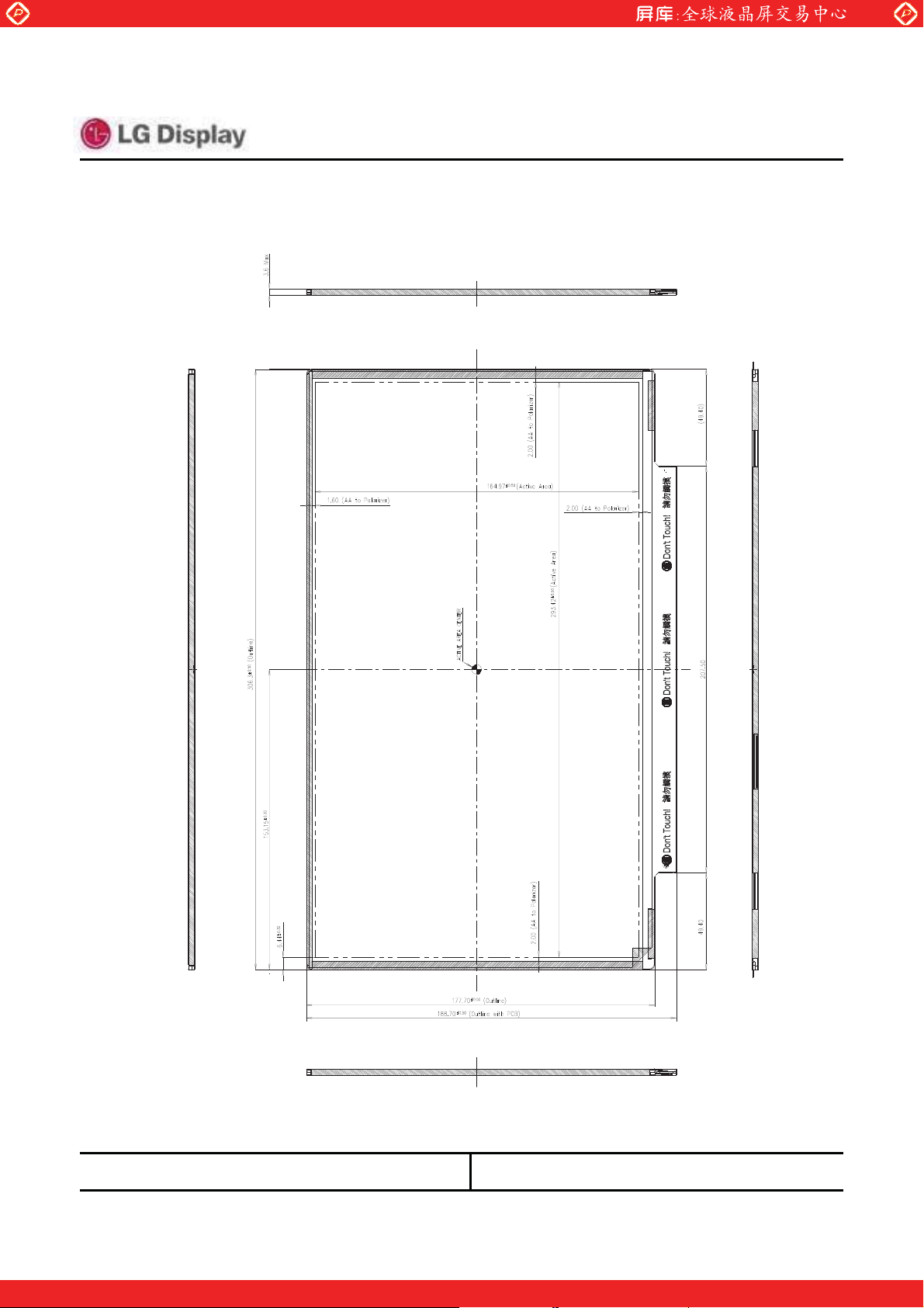
306.3ρ0.5 (H) u 177.7 ρ0.5 (W) / 3.6(Max) (D) (mm)Dimensional Outline
297.42(H) u168.57ρ0.5 (W) (mm)Bezel Opening
290g ( Typ.) / 300g ( Max.)Weight
1 2 1365 1366
1
2
BGRBGRBGRBGR
BGRBGRBGRBGR
BGRBGRBGRBGR
BGRBGRBGRBGR
0.2148mm
R G B
0.2148mm
BGR
: Pixel
: Sub-pixel
(Dots)
LG Display Co., Ltd.
Date: 2010. 08.11
One step solution for LCD / PDP / OLED panel application: Datasheet, inventory and accessory!
www.panelook.com
Page 5
Global LCD Panel Exchange Center
www.panelook.com
2.2. Dimensional Outline
( Front figure )
Specification Rev. 0.5
Note) Unit:[mm], General tolerance: r 0.5mm
5/ 56
UP
Down
* The size that related with metal bezel includes tape thickness (0.05mm)
LG Display Co., Ltd.
One step solution for LCD / PDP / OLED panel application: Datasheet, inventory and accessory!
Date: 2010. 08.11
www.panelook.com
Page 6
Global LCD Panel Exchange Center
www.panelook.com
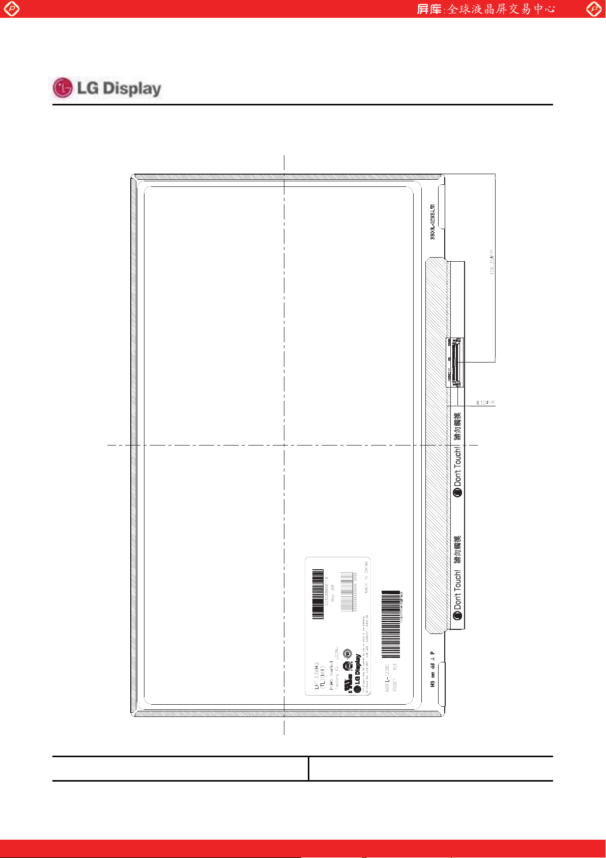
( Rear figure )
Specification Rev. 0.5
Note) Unit:[mm], General tolerance: r 0.5mm
6/ 56
LG Display Co., Ltd.
One step solution for LCD / PDP / OLED panel application: Datasheet, inventory and accessory!
Date: 2010. 08.11
www.panelook.com
Page 7
Global LCD Panel Exchange Center
www.panelook.com
Specification Rev. 0.5
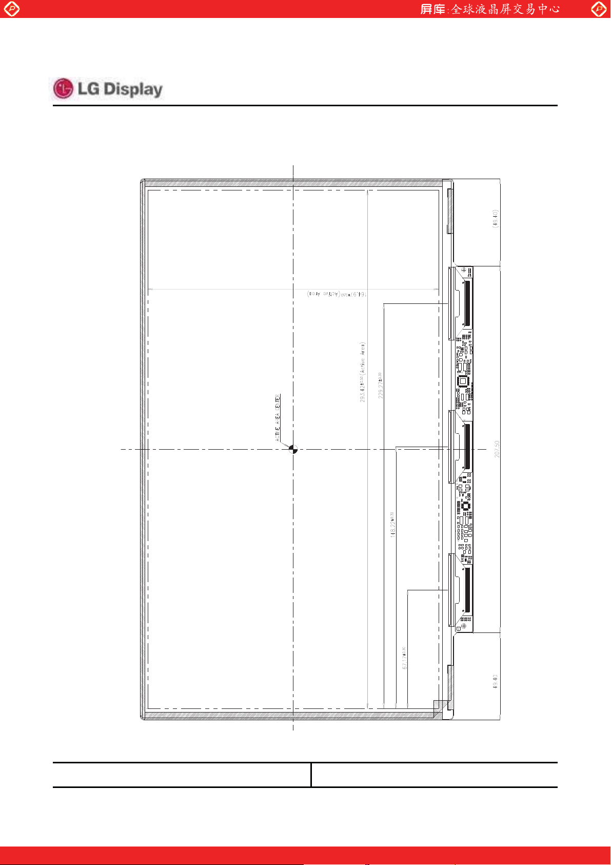
( Detail description of height of LCM back side & TAB Zone)
Note) Unit:[mm], General tolerance: r 0.5mm
7/ 56
LG Display Co., Ltd.
One step solution for LCD / PDP / OLED panel application: Datasheet, inventory and accessory!
Date: 2010. 08.11
www.panelook.com
Page 8
Global LCD Panel Exchange Center
www.panelook.com
Specification Rev. 0.5
3. Absolute Maximum Ratings
3.1. Absolute Ratings of Environment
MaxMinItem NoteSymbol
Operating Ambient Temperature
Operating Temperature for Panel
Storage Temperature
Operating Ambient Humidity
Storage Humidity
Air Pressure
Air Pressure
Altitude
Altitude
-
-
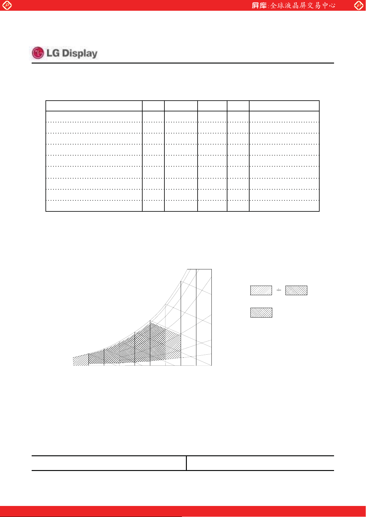
Note 1) Temperature and relative humidity range are shown in the figure below.
Wet bulb temperature should be 39qC Max, and no condensation of water.
Unit
8/ 56
(1)qC+500TOP
(2)qC+500-
(1)qC+60-20TSTG
(1)%RH9010HOP
(1)%RH9010HSTG
OperationkPa101.357-
Non-operationkPa101.312-
OperationKm3-
Non-operationKm12-
90% 80%
60%
Humidity[(%)RH]
Storage
40%
Operation
20%
10%
Wet Bulb
Temperature [
0
-20
]
20
10
10
20 30 40 50
60
50
40
30
60 70 800
Dry Bulb Temperature []
Note 2) The surface temperature caused by self heat radiation of cell itself is specified on this item.
LG Display Co., Ltd.
Date: 2010. 08.11
One step solution for LCD / PDP / OLED panel application: Datasheet, inventory and accessory!
www.panelook.com
Page 9
Global LCD Panel Exchange Center
www.panelook.com
3.2. Electrical Absolute Maximum
(1) TFT LCD Module
Power Supply Voltage
Logic Input Voltage
(2) Back Light Unit
LED Driver Supply Voltage
LED PWM / LED_EN Voltage
Specification Rev. 0.5
IN
V
PWM
V
LED_EN
9/ 56
MaxMinItem NoteSymbol
Unit
at 25 r 5qCV+4.0-0.3VDD
LVDS interfaceVVDD+0.3-0.3V
UnitMaxMinItem NoteSymbol
damage to the device V23-0.3VL
V6.0-0.3
LG Display Co., Ltd.
Date: 2010. 08.11
One step solution for LCD / PDP / OLED panel application: Datasheet, inventory and accessory!
www.panelook.com
Page 10
Global LCD Panel Exchange Center
www.panelook.com
3.3. Mechanical Ratings
Test Item NoteTest Conditions
Frequency Range 5 - 500 Hz, 14.7m/s
Mechanical Vibration
Mechanical Shock
LCD fix condition
-> See Note (2)
Pressure Resistanace
-> See Note (1)
at side-mout part
0.5Hrs each axis (X, Y, Z direction).
Frequency Range 5 - 500 Hz, 4.9m/s2( 0.5G) constant,
0.5Hrs each axis (X, Y, Z direction).
No Destruction with the force 196 N (20 kgf, 16 mm in diameter) to
the display surface at the vertical direction.
No Destruction with the force 294.2 N (30 kgf, 30 mm in diameter)
to the back of the display surface at the vertical direction.
Only the breakage of below items will not happen after test.
( Glass.LED & Circuit parts)
Input connector : With 50 times of connector trial there must be no
damage to the shape and functionaly.
M2 : Max 2.5 kgfAssured torque value
Specification Rev. 0.5
2
1.5G) constant,
70G, Pulse width 11ms, Sine Wave rX, rY, rZ direction.
* Note) Normal function is only checking points.
2
(10G), Pulse width 11 ms, Sine Wave, rX, rY, rZ direction.
10 / 56
Non Operation
Operation
Non Operation* 240G, Pulse width 2 ms, Sine Wave, rX, rY, rZ direction.
Operation98 m/s
Non Operation
Fig 1-1
Fig 1-2
Fig 1-3
Non OperationConnector tension test
Non Operation
Tapping area : All bezel(Metal cover) side,
Tapping test
LCD: Full-screen gray (L32).
“Ripple (Pooling )” can not be seen in Active Area
Tapping Force: Max 3kgf.cm
Definitions of failure for judgment shall be as follows:
(1) Function of the module should be maintained.
(2) Current consumption should be smaller than the specified value.
(3) Appearance and display quality should not have distinguished degradation.
(4) Luminance should be larger than the minimum value specified in optical specification.
Non Operation15 times under Max. torqueRescrewed test
Operation
LG Display Co., Ltd.
Date: 2010. 08.11
One step solution for LCD / PDP / OLED panel application: Datasheet, inventory and accessory!
www.panelook.com
Page 11
Global LCD Panel Exchange Center
www.panelook.com
Note 1)
Specification Rev. 0.5
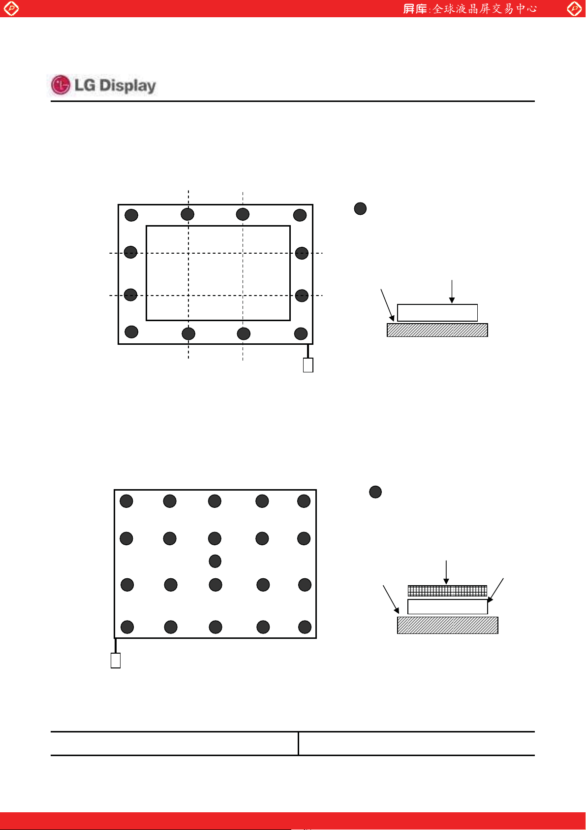
(1) The compression condition of front side
(a) Compression point : 12 points ( refer to Fig 1-1)
(b) Compression condition: 20kgf, 3 sec, Tool diameter: 16 mm in diameter (refer to Fig 1-3)
COMPRESSION POINT
LCDFlat plate
11 / 56
[ Fig 1-1 ]
(2) The compression condition of rear side
(a) Compression point : 21 points ( refer to Fig 1-2 )
(b) Compression condition : 30kgf, 3 sec, Tool radius: 30 mm in diameter ( refer to Fig 1-3)
COMPRESSION POINT
ABS natural 2.0t
Flat plate
LCD
[ Fig 1-2 ]
LG Display Co., Ltd.
Date: 2010. 08.11
One step solution for LCD / PDP / OLED panel application: Datasheet, inventory and accessory!
www.panelook.com
Page 12
Global LCD Panel Exchange Center
www.panelook.com
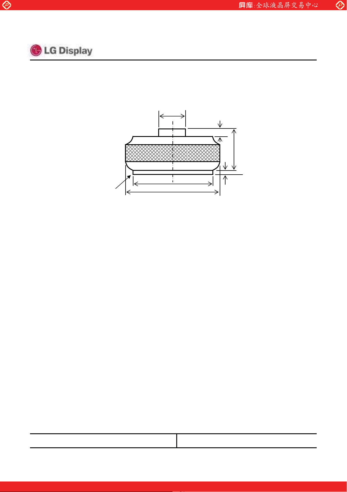
Rubber sheet
Specification Rev. 0.5
10mm in diameter
B
A
[ Fig 1-3 ]
12 / 56
10
16
1.5
(3) Dimension of the compression jig
(a) compression jig for front side A = 16 mm in diameter
B = 16 mm in diameter
(b) compression jig for rear side A = 30 mm in diameter
B = 28 mm in diameter
LG Display Co., Ltd.
Date: 2010. 08.11
One step solution for LCD / PDP / OLED panel application: Datasheet, inventory and accessory!
www.panelook.com
Page 13
Global LCD Panel Exchange Center
www.panelook.com
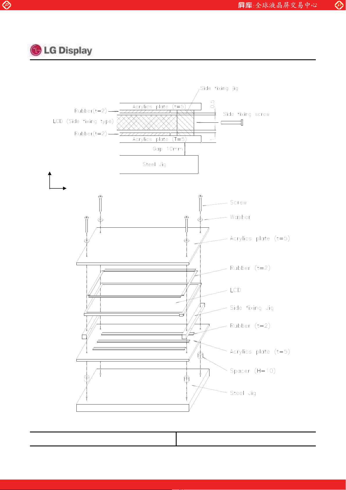
Note 2) LCD fixing condition for z direction.
Z
Y X
Specification Rev. 0.5
13 / 56
LG Display Co., Ltd.
One step solution for LCD / PDP / OLED panel application: Datasheet, inventory and accessory!
Date: 2010. 08.11
www.panelook.com
Page 14
Global LCD Panel Exchange Center
www.panelook.com
3.4. The Others
(1) Static electricity pressure resistance
(2) Sound noise
There should be no uncomfortable noise.
Being used under whatever surrounds, when power on/off, the panel should not generate
uncomfortable noise. And regarding specified values are negotiated if it is needed.
(3) Open / Short
No smoke, no fiery at any open/ short test
(4) MTBF : 50,000 Hr (except for backlight LED)
Specification Rev. 0.5
14 / 56
Non OperationOperationItem Testing conditions
r 10 kV8KV150pF, 330 ohmContact discharge
20 KV15KV150pF, 330 ohmAir discharge
LG Display Co., Ltd.
Date: 2010. 08.11
One step solution for LCD / PDP / OLED panel application: Datasheet, inventory and accessory!
www.panelook.com
Page 15
Global LCD Panel Exchange Center
www.panelook.com
Specification Rev. 0.5
15 / 56
4. Optical Characteristics
4.1. Test Conditions
Ambient Temperature : Ta 25r5qC
Ambient Humidity : Ha 65r20%RH
Supply Voltage : VDD 3.3V
Input Signal : According to typical value in "Electrical Characteristics"
LED Driver Supply Voltage : VLED = 12V
LED PWM Duty : DPWM = 100%
The measuring method is shown in 4.2. The following items are measured under stable conditions. The opti
cal characteristics should be measured in a dark room ( Screen illuminance < 2 lx ) or equivalent state with t
he methods shown in Note (6).
4.2. Optical Specifications
NoteUnitMax.Typ.Min.ConditionsSymbolItem
Contrast Ratio
(Center 1 Point)
Response Time
Average luminance
(5 Point Average)
Cross Modulation
Red
Luminance
Uniformity
Chromaticity
Viewing
Angle
13 Points CR Variation
Green
Blue
White
Hor.
Ver.
Hor.
Ver.
ON+tOFF
ON
t
OFF
L
SHA
Rx
Ry
Gx
Gy
Bx
By
Wx
Wy
T
L
T
R
T
up
T
Low
T
L
T
R
T
up
T
Low
ǬW13 Points White Variation
R
T=0q, I=0q
Viewing
normal angle
CR>=10
CR>=5
T=0q, I=0q
Viewing
normal angle
I = 180
I = 0q
I = 90q
I = -90q
I = 180
I = 0q
I = 90q
I = -90q
40
40
10
30
50
50
10
30
45
45
15
35
55
55
15
35
ms2516t
95.5t
-200170Y
ms (3)
ms1610.5
2
cd/m
0.6070.5770.547
0.3770.3470.317
0.3680.3380.308
0.5910.5610.531
0.1890.1590.129
-
0.1570.1270.097
0.3430.3130.283
0.3590.3290.299
-
-
-
deg.
-
-
-
-
(2), (6)--350300CR
=12V
*V
LED
=100%
D
PWM
Gray Scale Level
= L63 (White)
(5)%2.0--D
(1), (6)
PR650
Only for
Color
Coordinate
(Color Coordinate of
the R,G,B is based
on LGD’s equipment,
and Color Coordinate
of the W is based on
LGD’s equipment)
(7)1.6--
(7)2.0--ǬC
(8)2.0--dLWhite Variation
LG Display Co., Ltd.
Date: 2010. 08.11
One step solution for LCD / PDP / OLED panel application: Datasheet, inventory and accessory!
www.panelook.com
Page 16

Global LCD Panel Exchange Center
www.panelook.com
Specification Rev. 0.5
16 / 56
Attach the LED current – Luminance characteristics. The range of LED current is shown in 3.2 (2)
A. Present CR Variation(13Point) Spec is based on PR-880 Equipment and can be changed by the
measuring equipment.
NoteUnitMax.Typ.Min.ConditionsGray levelItem
100100100
88746055
6852.4936.847
50
33
21.5
11.6
4.9
0.90.120.000
%
(1), (6)
(Center 1 Point)
Normalized luminance
at each gray level
63
T=0q, I=0q
Viewing
normal angle
34.822039
21.019.531
12.213.523
5.360.9515
1.450.097
At normal viewing direction, during displaying the L0-L63 gray scale bar, luminance intensity inversion
can not be seen.
Note 1) Definition of viewing angle T and I
I
= 180
q
I
= 270
,
Left
q
Down
,
Note 2) LCD fixing condition for z direction.
The contrast ratio can be calculated by the following expression.
Contrast Ratio (CR) = L63 / L0
L63 : Luminance on the white raster (gray scale level L63)
L 0 : Luminance on the black raster (gray scale level L0)
Normal
T
Measurement
Direction
I
Y
I
= 90q, Up
I
q
= 0
,
Right
LG Display Co., Ltd.
Date: 2010. 08.11
One step solution for LCD / PDP / OLED panel application: Datasheet, inventory and accessory!
www.panelook.com
Page 17

Global LCD Panel Exchange Center
www.panelook.com
Specification Rev. 0.5
Note 3) Definition of response time
%
100
90
Optical
Response
10
0
Bright Bright
Note 4) Definition of surface luminance of white
Measure the luminance of white at Center point. Surface luminance of white Y
Ton
17 / 56
Toff
Dark
L
Note 5) Definition of Cross Modulation (D
= | YB–YA| / YAu100 (%)
D
SHA
Where:
= Luminance of measured location without darkest gray pattern (cd/m2)
Y
A
Y
= Luminance of measured location with darkest gray pattern (cd/m2)
B
(0, 0)
Gray Level 42
VIEW AREA
YA(683, 192)
(1366, 768)
SHA
)
Gray Level 0
Gray Level 42
(0, 0)
VIEW AREA
(106, 96)
YA(683, 192)
(342, 384)
(1366, 768)
LG Display Co., Ltd.
Date: 2010. 08.11
One step solution for LCD / PDP / OLED panel application: Datasheet, inventory and accessory!
www.panelook.com
Page 18

Global LCD Panel Exchange Center
www.panelook.com
Note 6) Measuring setup
The measurement suppose to be executed after stabilized the panel at given temperature during 30
min. The measurement shall be executed 30 minutes after lighting at rating. The luminance of white
should be typical luminance ( Typical Condition IL=6.0mA ). In order to stable the luminance, LCD s
hall not be got winds.
LCD module
LCD panel
Center of the screen
Specification Rev. 0.5
( Field of view = 1 deg)
500 mm
18 / 56
Light Shield Room
( Screen luminance < 2 lx)
Photometer
(Prichard 880 or equivalent)
Note 7) Definition of 13 points white variation GW, CR variation GC
GW = Maximum luminance of 13 points / Minimum luminance of 13 points
GC
= Maximum CR 13 points / Minimum CR of 13 points
R
Horizontal Line number [pixel]
Vertical Line number [pixel]
0
192
384
576
768
45
723
0
45
6
9
11
342 683 1025 1366
7 8
2
1
4
12
3
5
Active area
R
1321
: test point
10
13
LG Display Co., Ltd.
Date: 2010. 08.11
One step solution for LCD / PDP / OLED panel application: Datasheet, inventory and accessory!
www.panelook.com
Page 19

Global LCD Panel Exchange Center
www.panelook.com
Specification Rev. 0.5
Note 8) Definition of White Variation dL : measure the luminance of white at 13 u11 points.
dL = [ | L(x,y) – L(x+I, y+j) | / ( L(x,y) u D(x+I, y+j) ) ] u 100 (%/mm)
where 2 d x d 15, 2 d y d 11, I = r 1, j = r 1
2.14mm
10.9mm
17.5mm
11.6mm
17.5mm
L(x-1,y-1)
12
D(x+1,y-1)
L(x,y)
19 / 56
L(x+1,y-1)
L(x+1,y+1)
Active area
Measuring Spot 16
( Field of View : 2deg. Measuring Distance : 500 mm )
I17.5
LG Display Co., Ltd.
Date: 2010. 08.11
One step solution for LCD / PDP / OLED panel application: Datasheet, inventory and accessory!
www.panelook.com
Page 20

Global LCD Panel Exchange Center
www.panelook.com
Specification Rev. 0.5
20 / 56
5. Electrical Characteristics
5.1. TFT LCD module
NoteUnitMax.Typ.Min.SymbolItem
Power Supply Voltage
Differential Input
Threshold Voltage
Rush Current
Power Supply
Current
High
Low
White(L63)
Mosaic
Max. Pattern
DD
RUSH
I
DD
255225195
Note 1) The module should be always operated within these ranges. The "Typ." shows the recommendable
value.
Note 2) Recommended LVDS transmitter : SN75LVDS84 (made by TI )
LVDS receiver included in this module is SW0617.(1 chip)
Note 3) Typical condition as follows. : fV= 60Hz, fDCLK = 69.3 MHz, V
= 3.3V, DC current.
DD
Note 4) Power dissipation check pattern.
V3.63.33.0V
mV+100-Vth
mV---100Vtl
mA
(5)A1.5--I
(3), (4) (a)
(3), (4) (b)365315265
(3), (4) (c)470410350
(a) White pattern
Active Area
(C) Max. pattern
Active Area
(b) Mosaic pattern
Display Brightest Gray scale
Display Darkest Gray scale
G BR
LG Display Co., Ltd.
Date: 2010. 08.11
One step solution for LCD / PDP / OLED panel application: Datasheet, inventory and accessory!
www.panelook.com
Page 21

Global LCD Panel Exchange Center
www.panelook.com
Specification Rev. 0.5
Note 5) Measuring condition of rush current.
21 / 56
rising time is 500us
V
DD
GND
LG Display Co., Ltd.
0.1 V
DD
0.9 V
3.3V
DD
Date: 2010. 08.11
One step solution for LCD / PDP / OLED panel application: Datasheet, inventory and accessory!
www.panelook.com
Page 22

Global LCD Panel Exchange Center
www.panelook.com
5.2. Backlight Unit
BACKLIGHT : ( with LED Driver)
PWM Jitter
PWM High Level Voltage
PWM Low Level Voltage
Specification Rev. 0.5
SymbolParameter
LEDLED Power Input Voltage
LEDLED Power Input Current
LEDLED Power Consumption
LED_PLED Power Inrush Current
-
PWMPWM Impedance
PWMPWM Frequency
PWM_H
PWM_L
PWMLED_EN Impedance
22 / 56
Values
NotesUnit
MaxTypMin
1V21.012.07.0V
2mA220200-I
3W2.62.4-P
4mA1000--I
5%100-5PWM Duty Ratio
6%0.2-0
kȳ604020Z
7Hz20001000200F
V5.3-3.0V
V0.3-0V
kȳ604020Z
LED_EN_HLED_EN High Voltage
LED_EN_LLED_EN Low Voltage
V5.3-3.0V
V0.3-0V
8Hrs--12,000Life Time
1. This impedance value is needed for proper display and measured form LVDS Tx to the mating connector.
2. The measuring position is the connector of LCM and the test conditions are under 25.
3. The current and power consumption with LED Driver are under the Vled = 12.0V , 25, Dimming of
Max luminance and White pattern with the normal frame frequency operated(60Hz).
4. The below figures are the measuring Vled condition
and the Vled control block LGD used.
VLED control block is same with Vcc control block.
Rising time
LED
V
0V
10%
90%
12.0V
0.5ms
5. The operation of LED Driver below minimum dimming ratio may cause flickering or reliability issue.
6. If Jitter of PWM is bigger than maximum, it may induce flickering.
7. This Spec. is not effective at 100% dimming ratio as an exception because it has DC level equivalent
to 0Hz. In spite of acceptable range as defined, the PWM Frequency should be fixed and stable for
more consistent brightness control at any specific level desired.
8. The life time is determined as the time at which the typical brightness of LCD is 50% compare to that of
initial value at the typical LED current. These LED backlight has 4 strings on it and the typical current of
LED’s string is base on 18mA.
LG Display Co., Ltd.
Date: 2010. 08.11
One step solution for LCD / PDP / OLED panel application: Datasheet, inventory and accessory!
www.panelook.com
Page 23

Global LCD Panel Exchange Center
ൎ
www.panelook.com
Specification Rev. 0.5
5.3. Regulation
The set (which LCD module is assembled into) should conform to the regulations below.
(1) EMC Regulations.
a) ANSI C63.4
b) CISPR 22
c) CISPR 13
(2) Safety Regulations (Only LCD)
a) UL 60950-1, Second Edition, Underwriters Laboratories Inc.
b) CAN/CSA C22.2 No.60950-1-07, Second Edition, Canadian Standards Association.
c) EN 60950-1:2006 + A11:2009, European Committee for Electrotechnical Standardization (CENELEC).
d) IEC 60950-1:2005, Second Edition, The International Electrotechnical Commission (IEC).
(3) Environment
a) RoHS, Directive 2002/95/EC of the European Parliament and of the council of 27 January 2003
(4) Material list concerning
23 / 56
TCON
DC/DC
LED
Driver
TCON OUTPUT
(Data Output)
Power
V
(2.5V)
cc
Control IC for
Power supply
Switching
Diode
Schottky
Barrier Diode
Control IC for
LED
R12, R13,
R14, R15
NRS4012T100ML2, L3Inductor
NRS4012T100ML4Inductor
Resistor
SW5024US1
DAN217UD11
ADD5201US3
100
2.5VTCONUC1
SW5024, Siliconworks, NBPC,
Boost+LDO+L/S+OP-Amp+PVcom+D/C+GPM,
TQFN (6x6), R/TP, 48 pin
DC/DC Switching frequency
(400Khz ~ 1200Khz)
0.75ABAT750-7-FD3, D10
10 uH20% (Inductance)
0.310ೱ20% (DC Resistance)
0.95A Max (Rated DC Current)
ADD5201, ANALOG DEVICE, 21V, 8CH, -,
LFCSP, R/TP, 28, NBPC
10 uH20% (Inductance)
0.310ೱ20% (DC Resistance)
0.95A Max (Rated DC Current)
MakerRatingProductSilkItem
ROHM,
Samsung
Elec., Walsin
Siliconworks
Siliconworks
DIODES
DIODES
KTY
Analog
Device
KTY
LG Display Co., Ltd.
Date: 2010. 08.11
One step solution for LCD / PDP / OLED panel application: Datasheet, inventory and accessory!
www.panelook.com
Page 24

Global LCD Panel Exchange Center
www.panelook.com
6. Block Diagram
User connector
LVDS
1port
40
Pin
VCC
VLED
LED_EN
PWM
Specification Rev. 0.5
EEPROM Block
EEPROM Block
for EDID
for EDID
EEPROM Block
EEPROM Block
for Tcon Operating
for Tcon Operating
Timing Control
Timing Control
(Tcon) Block
(Tcon) Block
DVCC
Power
Power
Block
Block
LED Driver
LED Driver
Block
Block
TCLKs
M
i
n
i
-
L
V
D
S
AVCC, AVDD
VGH, VGL, GMA
GIP CLKs, DSC
VOUT_LED
FB1~4
ࣿࣜࣜ ࣜࣜࣜ
1
TFT-LCD Panel
(HD, GIP, TN)
768
Source Driver
(Flat)
LED Backlight Ass’y
24 / 56
1366
LG Display Co., Ltd.
Date: 2010. 08.11
One step solution for LCD / PDP / OLED panel application: Datasheet, inventory and accessory!
www.panelook.com
Page 25

Global LCD Panel Exchange Center
www.panelook.com
Specification Rev. 0.5
25 / 56
7. Input Terminal Pin Assignment
7.1. TFT LCD module
This LCD employs two interface connections, a 40 pin connector is used for the module electronics interface
and the other connector is used for the integral backlight system.
Table 3. MODULE CONNECTOR PIN CONFIGURATION (CN1)
NotesDescriptionSymbolPin
20
23
24
26
27
29
30
31
32
33
34
35
36
37
38
39
40
NC
NC
NC
NC
NC
NC
NC
NC
GND
GND
GND
NC
LED_EN
NC
No Connection`NC1
LCD Logic and driver power (3.3V Typ.)VCC2
LCD Logic and driver power (3.3V Typ.)VCC3
DDC Power (3.3V)V EEDID4
No ConnectionNC5
DDC ClockClk EEDID6
DDC DataDATA EEDID7
Negative LVDS differential data inputORX0-8
Positive LVDS differential data inputORX0+9
LCM Ground GND10
Negative LVDS differential data inputORX1-11
Positive LVDS differential data inputORX1+12
LCM Ground GND13
Negative LVDS differential data inputORX2-14
Positive LVDS differential data inputORX2+15
LCM Ground GND16
Negative LVDS differential clock inputORXC-17
Positive LVDS differential clock inputORXC+18
LCM Ground GND19
No Connection
No Connection21
LCM Ground GND19
No Connection
No Connection
LCM Ground GND19
No Con
No Connection
LCM Ground GND19
No Connection
No Connection
LCM Ground (LED Backlight Ground)
LCM Ground (LED Backlight Ground)
LCM Ground (LED Backlight Ground)
No Connection
System PWM Signal input for dimmingPWM
LED Backlight On/Off
No Connection
LED Backlight Power (7V-21V)VLED
LED Backlight Power (7V-21V)VLED
LED Backlight Power (7V-21V)VLED
nection
1. Interface chips
1.1 LCD : SW, SW0617 (LCD Controller)
including LVDS Receiver
1.2 System : THC63LVDF823A
* Pin to Pin compatible with LVDS
2. Connector
2.1 LCD : UJU IS050-L40B-C10
2.2 Mating : 20453-#40E-## series
2.3 Connector pin arrangement
or equivalent
or equivalent
[LCD Module Rear View]
LG Display Co., Ltd.
Date: 2010. 08.11
One step solution for LCD / PDP / OLED panel application: Datasheet, inventory and accessory!
www.panelook.com
Page 26

Global LCD Panel Exchange Center
www.panelook.com
Specification Rev. 0.5
7.3. LVDS Transmitter
LVDS Transmitter : SN75LVDS84 (made by TI ) or compatible.
Pin Name
D1720
21
D1822
23
26 / 56
Require SignalsPin NamePin #Require SignalsPin #
R3D348R4D41
R2D247VccVcc2
GNDGND46R5D53
R1D145G0D64
R0D044GNDDND5
NCNC43G1D76
LVDS GNDLVDS GND42G2D87
Y0M41VccVcc8
Y2M35NCNC14
A0M
A0PY0P40G3D99
A1MY1M39G4D1010
A1PY1P38GNDGND11
LVDS VccLVDS Vcc37G5D1112
LVDS GNDLVDS GND36B0D1213
A2M
A2PY2P34B1D1315
CLKMCLKOUTM33B2D1416
CLKPCLKOUTP32GNDGND17
LVDS GNDLVDS GND31B3D1518
PLL GNDPLL GND30B4D1619
PLL VccPLL Vcc29B5
PLL GNDPLL GND28VccVcc
SHDNSHDN27HSYNC
DclkCLKIN26VSYNCD19
DE(Data Enable)D2025GNDGND24
LG Display Co., Ltd.
Date: 2010. 08.11
One step solution for LCD / PDP / OLED panel application: Datasheet, inventory and accessory!
www.panelook.com
Page 27

Global LCD Panel Exchange Center
www.panelook.com
Specification Rev. 0.5
7.4. Timing Diagrams of LVDS Transmission
Switching Characteristic
VCC = 3.0 ~ 3.6V, Ta = -10 ~ +70
Transmitter
Parameter UnitMax.Typ.Min.Symbol
27 / 56
ns5--CLK IN Transition TimetTCIT
ns32.4T14.7CLK IN PeriodtTCP
ns0.6T0.5T0.4TCLK IN High TimetTCH
ns0.6T0.5T0.4TCLK IN Low TimetTCL
ns-14.2-CLK IN to TCLK +/- DelaytTCD
ns--3.0TTL Data Setup to CLK INtTS
ns--1.5TTL Data Hold from CLK INtTH
ns1.50.70.26LVDS Transition TimetLVT
ns0.20-0.2Output Data Position 0 (T= 15.38ns)tTOP1
nsT/7 + 0.2T/7T/7 - 0.2Output Data Position 1 (T= 15.38ns)tTOP0
ns2T/7 + 0.22T/72T/7 - 0.2Output Data Position 2 (T= 15.38ns)tTOP2
ns3T/7 + 0.23T/73T/7 - 0.2Output Data Position 3 (T= 15.38ns)tTOP3
ns4T/7 + 0.24T/74T/7 - 0.2Output Data Position 4 (T= 15.38ns)tTOP4
ns5T/7 + 0.25T/75T/7 - 0.2Output Data Position 5 (T= 15.38ns)tTOP5
ns6T/7 + 0.26T/76T/7 - 0.2Output Data Position 6 (T= 15.38ns)tTOP6
ns10--Phase Lock Loop SettTPLL
LG Display Co., Ltd.
Date: 2010. 08.11
One step solution for LCD / PDP / OLED panel application: Datasheet, inventory and accessory!
www.panelook.com
Page 28

Global LCD Panel Exchange Center
www.panelook.com
AC Timing Diagrams
Transmitter Device
CLK IN
TxD - Tx6
Tx +/-
tTCP
tTCH tTCL
2.0V
tTS
2.0V
0.8V
DATA VALID
Specification Rev. 0.5
2.0V
0.8V
tTH
2.0V
0.8V
tTCD
2.0V 2.0V
0.8V
0.8V
28 / 56
Tx0Tx1Tx4 R G B Tx2Tx5Tx6
TCLK+
V diff=0V
tTOP1
tTOP0
tTOP6
tTOP5
tTOP4
tTOP3
tTOP2
LG Display Co., Ltd.
Date: 2010. 08.11
One step solution for LCD / PDP / OLED panel application: Datasheet, inventory and accessory!
www.panelook.com
Page 29

Global LCD Panel Exchange Center
www.panelook.com
Specification Rev. 0.5
7.5. Input Signal, Basic Display Colors and Gray Scale of each Color
Input Color Data
Color
MSB LSB
RED
Black
Red
Green
Basic
Color
Blue
Cyan
Magenta
Yellow
White
RED (00)
RED (01)
RED
…
RED (62)
RED (63)
GREEN (00)
GREEN (01)
GREEN
...
GREEN (62)
GREEN (63)
BLUE (00)
BLUE (01)
BLUE
…
BLUE (62)
BLUE (63)
Note 1) 0: Low level voltage, 1: High level voltage
MSB LSB
GREEN
29 / 56
BLUE
MSB LSB
B5 B4 B3 B2 B1 B0G5 G4 G3 G2 G1 G0R5 R4 R3 R2 R1 R0
0 0 0 0 0 00 0 0 0 0 00 0 0 0 0 0
0 0 0 0 0 00 0 0 0 0 01 1 1 1 1 1
0 0 0 0 0 01 1 1 1 1 10 0 0 0 0 0
1 1 1 1 1 10 0 0 0 0 00 0 0 0 0 0
1 1 1 1 1 11 1 1 1 1 10 0 0 0 0 0
1 1 1 1 1 10 0 0 0 0 01 1 1 1 1 1
0 0 0 0 0 01 1 1 1 1 11 1 1 1 1 1
1 1 1 1 1 11 1 1 1 1 11 1 1 1 1 1
0 0 0 0 0 00 0 0 0 0 00 0 0 0 0 0
0 0 0 0 0 00 0 0 0 0 00 0 0 0 0 1
………
0 0 0 0 0 00 0 0 0 0 01 1 1 1 1 0
0 0 0 0 0 00 0 0 0 0 01 1 1 1 1 1
0 0 0 0 0 00 0 0 0 0 00 0 0 0 0 0
0 0 0 0 0 00 0 0 0 0 10 0 0 0 0 0
………
0 0 0 0 0 01 1 1 1 1 00 0 0 0 0 0
0 0 0 0 0 01 1 1 1 1 10 0 0 0 0 0
0 0 0 0 0 00 0 0 0 0 00 0 0 0 0 0
0 0 0 0 0 10 0 0 0 0 00 0 0 0 0 0
………
1 1 1 1 1 00 0 0 0 0 00 0 0 0 0 0
1 1 1 1 1 10 0 0 0 0 00 0 0 0 0 0
LG Display Co., Ltd.
Date: 2010. 08.11
One step solution for LCD / PDP / OLED panel application: Datasheet, inventory and accessory!
www.panelook.com
Page 30

Global LCD Panel Exchange Center
www.panelook.com
Specification Rev. 0.5
8. Interface Timing
8.1. Timing Parameters
This is the signal timing required at the input of the User connector. All of the interface signal timing should be
satisfied with the following specifications and specifications of LVDS Tx/Rx for its proper operation
Hsync
Vsync
Data
Enable
FrequencyDCLK
Slow Refresh RateDCLK
Period
Width
Width-Active
Period
Width
Width-Active
Horizontal back porch
Horizontal front porch
Vertical back porch
Vertical front porch
CLK
CLK
HP
WH
VP
WV
HBP
HFP
VBP
VFP
HA
VA
167416421450t
12411228t
136613661366tw
792786775t
532t
768768768tw
13612828t
483628t
12104t
751t
.
tCLK
tHP
tCLK
tHP
30 / 56
NoteUnitMax.Typ.Min.SymbolITEM
@ 60HzMHz79.577.467.4f
@ 40HzMHz5351.6244.95f
Appendix) All reliabilities are specified for timing specification based on refresh rate of 60 Hz.
Even though actual performance in 50Hz and 40Hz for low power is displayed normally,
remark and inform to user that display quality in 40 Hz and 50 Hz is out of guarantee range.
Data Enable, Hsync, Vsync
tCLK
DCLK
Hsync
t
WH
t
HBP
0.5 Vcc
t
HP
High: 0.7VCC
Low: 0.3VCC
tWHA
Condition : VCC =3.3V
t
HFP
Data Enable
t
VP
t
WV
Vsync
t
VBP
tWVA
t
VFP
Data Enable
LG Display Co., Ltd.
Date: 2010. 08.11
One step solution for LCD / PDP / OLED panel application: Datasheet, inventory and accessory!
www.panelook.com
Page 31

Global LCD Panel Exchange Center
www.panelook.com
8.3. Power On/Off Sequence
Power Supply Input
VCC
0V
Interface Signal, V
LVDS
LED BL
On/Off Control Signal
LED_EN
i
0V
0V (Off)
90%
Specification Rev. 0.5
T
T
1
2
T
5
T
9
Valid Data
3.0V
3.0V
31 / 56
90%
10%10%
T
T
3
7
T
6
T
10
T
4
8
T
12
Valid Data
T
11
90%
T
10%
13
LED BL
Dimming Control Signal
PWM
LED Driver Input Voltage
VLED
0V (Low)
0V
T
90%
10%
Table 6. POWER SEQUENCE TABLE
Logic
Parameter
1
2
3
4
5
6
7
Value
Max.Typ.Min.
Units
ms10-0.5T
ms50-0T
ms50-0T
ms--200T
ms--200T
ms--0T
LED
Parameter
8
9
10
11
12
13
ms10-0.5T
Value
Note)
1. Do not insert the mating cable when system turn on.
2. Valid Data have to meet “3-3. LVDS Signal Timing Specifications”
3. LVDS, LED_EN and PWM need to pull-down condition on invalid status.
4. LGD recommend the rising sequence of VLED after the Vcc and valid status of LVDS turn on.
Max.Typ.Min.
Units
ms--10T
ms--10T
ms--10T
ms--10T
ms--0.5T
ms5000-0.1T
LG Display Co., Ltd.
Date: 2010. 08.11
One step solution for LCD / PDP / OLED panel application: Datasheet, inventory and accessory!
www.panelook.com
Page 32

Global LCD Panel Exchange Center
www.panelook.com
Specification Rev. 0.5
9. Cosmetic Specification
9.1. Sampling
A.Q.L (Acceptable Quality Level ): MIL-STD, 105E Level II,
Major: 0.65 , Minor: 1.5
9.2. Conditions of Inspections
(1) Ambient Temperature : 25r5qC
(2) Ambient Humidity : 65r20%RH
(3) Illumination : 200 – 500 Lux ( nominal 350 Lux ) under the fluorescent Lamp.
(4) Viewing Distance: Approximately 30cm by the eyes of the inspector from the module
(5) Viewing angle : The surface of the module and the inspector’s line shall be at 90 r 45 degrees.
(6) Display pattern: Pure Red, Green, Blue, Black, White, Gray level 0 - 63
9.3. Defect modes
DescriptionDefect Mode
Points on the display which appear dark / bright and remain unchanged in sizeDark / Bright spots
Lines on the display which appear dark / bright and remain unchanged in sizeDark / Bright lines
Polarizer scratch
Polarizer dent
Ripple (Pooling )
When the unit is lit a light , line is seen across a darker background; line does not vary
in size
When the unit is lit a light, light (white) spots appear against a darker background, and
do not vary in size
A sub-pixel (R,G,B dot) stuck off / onBright / dark dot
Diagonal lines that appear gray with the display patterns dark and vary in sizeRubbing line
When the unit lights, lines in the minor (Vertical ) or major (Horizontal) axis appear dimDim line
When the unit lights, lines in the both minor and major axis do not appearCross line
Interference can not be seen with any bright plane display at any viewing angleInterference
When displaying sub-pixel checker(gray level and darkest gray), flicker can not be seenFlicker
Tapping Test, Tapping area : All bezel(Metal cover) side, LCD: Full-screen gray (L32)
“Ripple (Pooling )” can not be seen in Active Area
32 / 56
9.4. Mechanical Inspection
(1) Light leakage: No light leakage between metal chassis (bezel) and glass
(2) No sharp edge
(3) The mounting holes: No Changed (Side fixed type)
(4) PCB Appearance: No pattern peeling snapping / No electrically short
If there are repair portions, the repair portions on PCB is covered by epoxy resign
(5) Soldering: No cold solder joint, lead move when pulled
(6) Bezel, Frame, Connectors: No distinct stain, rust or scratch, no pin bending
LG Display Co., Ltd.
One step solution for LCD / PDP / OLED panel application: Datasheet, inventory and accessory!
Date: 2010. 08.11
www.panelook.com
Page 33

Global LCD Panel Exchange Center
www.panelook.com
9.5. Visual Inspection
Dark / bright spot
Dark / Bright lines
L
Polarizer scratch
L
Specification Rev. 0.5
Reject (mm)Count (mm)Defect type
D
W
W
0.2 < D d 0.5
N d 3
0.05 < W d 0.1
0.3 < L d 3.0
N d 3
0.01 < W d 0.1
0.3 < L d 0.5
N d 3
D > 0.5
W > 0.1
L > 3.0
W > 0.1
L > 0.5
33 / 56
Polarizer dent / bubble
D
0.2 d D d 0.5
N d 3
Not allowedRubbing defect
Not allowedDim line
D > 0.5
N > 7N d 7Maximum allowable number of defects
[ D : diameter, W : width, L : length, N : count ]
Note 1) Inspection area should be within bezel opening.
Note 2) Dusts which are bigger not less than 0.10mm (0.1dW) shall be judged by "Average Diameter".
Note 3) Scratches which are bigger not less than 0.05mm (0.05dW) shall be judged by "Average Diameter".
Average Diameter D = (a+b)/2 (mm)
a
b
LG Display Co., Ltd.
Date: 2010. 08.11
One step solution for LCD / PDP / OLED panel application: Datasheet, inventory and accessory!
www.panelook.com
Page 34

Global LCD Panel Exchange Center
www.panelook.com
Specification Rev. 0.5
9.6. Electrical Inspection
(1) Dot defect
Defect type
Bright dots
Three or more adjacent
Dark dots
Maximum distance
between defects
Not allowedTwo adjacent
Not allowed
Not allowedThree or more adjacent
1) Inspection patterns for dot defect are Pure Red, Green, Blue, Black, and White.
2) Adjacent two dots will be counted as two dots.
3) The distribution of dot defects should be below. Average value of dot defect s should be less than 1.
RejectCount
N > 3N d 2Random
N > 5N d 4Random
N > 2N d 1Two adjacent
N > 6N d 5Maximum allowable number of dot defect
L d 15mmL>15.1mmBright - to - bright dot
L d 10mmL>10.1mmDark - to - dark dot
34 / 56
Quantity of LCD
0 1 2 3 4 5 6 7 8
Count of dot defect in a LCD
Required distribution of dot defect
4) The definition of 2 adjacent dots.
RGBRGBRG RGBRGBRG RGBRGBRG
LG Display Co., Ltd.
Average dot defect N
< 1
AVE
Date: 2010. 08.11
One step solution for LCD / PDP / OLED panel application: Datasheet, inventory and accessory!
www.panelook.com
Page 35

Global LCD Panel Exchange Center
www.panelook.com
Specification Rev. 0.5
(2) Light leakage
Light leakage can not be seen between metal chassis (bezel) and glass when displaying black plane.
(3) Image sticking
Image sticking pattern shall not be to persist longer than 1second after displaying following pattern 8
hours in the room temperature condition.
35 / 56
(4) Glue/stain/dirt
Glue, non-removable stain and dirt which are visible in the inspection area are not acceptable.
LG Display Co., Ltd.
Date: 2010. 08.11
One step solution for LCD / PDP / OLED panel application: Datasheet, inventory and accessory!
www.panelook.com
Page 36

Global LCD Panel Exchange Center
ྙ
ྚ
ྛ
ྜ
ྜྷ
ྡ
www.panelook.com
10. Packing
10.1. Carton
(1) Packing Form
Corrugated cardboard box and EPS Packing
(2) Packing Method
Packing Material : EPS (Expanded Polystyrene)
Packing Weight: : 1.3Kg
(1Box/30Module)
Packing weight, 30 pcs modules included :10.5kg
Specification Rev. 0.5
36 / 56
[^Z
Z][
ZZ_
͵Ͷ΄ʹͺ΅ͺͿͿ
ͽʹ͵;ΠΕΦΝΖ
ͳͲ
;Ͳ΅ͶͺͲͽ
ͽ͵Ͷ
;Ͳ΄ͼͺͿ;;Ή;΅ͲͶ
Ͷ΄ͲʹͼͺͿ΅ΣΒΪ΅
Ͷ΄ͲʹͼͺͿ΅ΣΒΪͳ΅΅;
΄ΈͳΉ
;;Ή;΅ͲͶ
Ͳ΅ΉͽͲͳͶͽ
ͲͽͲͽͳΒΘ
LG Display Co., Ltd.
Date: 2010. 08.11
One step solution for LCD / PDP / OLED panel application: Datasheet, inventory and accessory!
www.panelook.com
Page 37

Global LCD Panel Exchange Center
www.panelook.com
Specification Rev. 0.5
(3) Packing Specification
ConditionsItem
Random=1.50Grms, Non-Operating LCM, To driving way / 1hrPacking Vibration
Refer to below tablePacking Drop Test
Vibration frequency Drop Height
Bottom
side
Left
side
Front
side
Right
side
Rear
side
Top
side
drop test, repeat 3x.
Drop height according table.
drop test from 0.30 m
drop test from 0.30 m
drop test from 0.30 m
drop test from 0.30 m
drop test from 0.30 m
37 / 56
M a ss He i gh t M a ss He i gh t
[kg] [cm ] [kg] [cm]
170 15 43
270 16 42
367 17 41
463 18 40
560 19 39
657 20 38
755 21 38
853 22 37
951 23 37
10 49 24 36
11 48 25 36
12 46 26 36
13 45 27 36
14 44 28 – 50 35
(4) Package Label
Package label should be at least shown the following information.
a) TOSHIBA code name(G33C00068110) which will be numbered by Toshiba
b) Revision number which be numbered by LCD maker
c) Quantity
d) LCD maker
e) Model number which be numbered by LCD maker
f) Production Year / Month
(5) Location of Package label : 1 points ( Side )
1 Side (LABEL Position)
LG Display Co., Ltd.
Date: 2010. 08.11
One step solution for LCD / PDP / OLED panel application: Datasheet, inventory and accessory!
www.panelook.com
Page 38

Global LCD Panel Exchange Center
www.panelook.com
Specification Rev. 0.5
11. Labels and Other parts Exchange
11.1. LCD code Label on LCD
LCD code label should be at least shown the following information.
(1) TOSHIBA code name (G33C00068110) which will be numbered by Toshiba & Bar code
(Bar code : CODE-39 High-density )
(2) LGPL Serial number CODE ( numbered by LCD maker , less than equal 13 digits)
ABCDEFGHI JKLM
A,B,C : SIZE(INCH) D : YEAR
E : MONTH F ~ M : SERIAL NO.
Note
1. YEAR
Year
Mark
321
200452005
4
200320022001
2006720078200892009
6
38 / 56
2010
0
2. MONTH
Month
Mark
Apr5May
4
Jun7Jul8Aug9Sep
6
b) Location of Lot Mark
Serial No. is printed on the label. The label is attached to the backside of the LCD module.
This is subject to change without prior notice.
Oct
A
Nov
B
DecMarFebJan
C321
LG Display Co., Ltd.
Date: 2010. 08.11
One step solution for LCD / PDP / OLED panel application: Datasheet, inventory and accessory!
www.panelook.com
Page 39

Global LCD Panel Exchange Center
www.panelook.com
Example >
LABEL : 78mm X 37mm
Specification Rev. 0.5
TOSHIBA CODE
39 High-density
39 / 56
TOSHIBA
Revision Code
LGD Serial Number Code
128 High-density
The revision code is inserted in the label by Toshiba request. If the contents of the specification need to be
change under mass-production, the code can be revised after Toshiba’s approval. Although there is not
items in the contents of the specification, Toshiba can requests LGD to change the revision code.
11.2. Caution Texture and Labels on LCD
[Disposal of BL label]
LG Display Co., Ltd.
Date: 2010. 08.11
One step solution for LCD / PDP / OLED panel application: Datasheet, inventory and accessory!
www.panelook.com
Page 40

Global LCD Panel Exchange Center
www.panelook.com
11.3. Label Locations on LCD
Specification Rev. 0.5
40 / 56
11.4. Others
(1) Backlight repair parts kit : 6091L-1238C
PartNo.
Plate Bottom1
Cover Shield(S)2
Cover Shield(T)3
Cover Shield(L,R)4
Product Code
3300L-0332A
3550S-1024A
3550S-0910A
3550S-0921B
Geo rim
Geo rim
Geo rim
Maker
Qt’y
1
1
1
2
2Hwa sung7250L-0082ATape Adhesive5
36SSC6915L-0070ALED6
Note
LG Display Co., Ltd.
Date: 2010. 08.11
One step solution for LCD / PDP / OLED panel application: Datasheet, inventory and accessory!
www.panelook.com
Page 41

Global LCD Panel Exchange Center
www.panelook.com
Specification Rev. 0.5
(2) Package specification of Backlight repair parts kit
a) Individual packing
41 / 56
b) Master carton Packing method
c) Label
70
100
LG Display Co., Ltd.
Date: 2010. 08.11
One step solution for LCD / PDP / OLED panel application: Datasheet, inventory and accessory!
www.panelook.com
Page 42

Global LCD Panel Exchange Center
ᐭ
ᐭ
ᐭ
ᐭ
www.panelook.com
11.5. Instruction of changing the parts
11.5.1. Disassembly of Cover Shield
(1) ྙ Disassembly of Cover Shield (4 Point)
Caution: Pressure or stress should not be given on Source COF.
Cover Shield(L)
3550-0921B
Specification Rev. 0.5
42 / 56
Cover Shield(R)
3550-0910A
Cover Shield(R)
3550-0921B
Cover Shield(S)
3550S-1024A
LG Display Co., Ltd.
One step solution for LCD / PDP / OLED panel application: Datasheet, inventory and accessory!
Date: 2010. 08.11
www.panelook.com
Page 43

Global LCD Panel Exchange Center
ᐭ
www.panelook.com
11.5.2. Disassembly of Source PCB
(1) ྙ Disassembly of Source PCB.
Caution: Pressure or stress should not be given on PCB and COF.
Specification Rev. 0.5
43 / 56
SOURCE
PCB
LG Display Co., Ltd.
One step solution for LCD / PDP / OLED panel application: Datasheet, inventory and accessory!
Date: 2010. 08.11
www.panelook.com
Page 44

Global LCD Panel Exchange Center
www.panelook.com
Specification Rev. 0.5
11.5.3. Disassembly of Case top, Board Ass’y, Tape Adhesive, Light guide, Cover Ass’y
(1) ྙ Disassembly of Cover Shield (4Point)
(2) ྚ Disassembly of Screw for PCB fixing (2Point)
Caution: Maximum value of torque with Screw should be below 1.5kg.
(3) ྛ Disassembly of Board Ass’y.
Caution: This process should be made in Clean room with no scratch nor particle on Polarizer and
B/L Ass’y.
(4) ྜ Disassembly of Tape Adhesive used for Sheets fixing (4Point).
(5) ྜྷ Disassembly of Sheets, Light guide.
Caution: No penetration of foreign body is indispensable with no scratch on the surface of each
Sheets.
(5) ྞ Disassembly of Plate Ass’y
44 / 56
LED Array Ass’y
Plate Bottom
Reflector
Light Guide Panel
Supporter Main
Sheet
Board Ass’y
Cover Shield
Screw
PartNo.
LGP1
Diffuser Up2
Prism Up3
Prism Down4
Maker
Coretronic
KEIWA
Suntech
Suntech
Maker P/N
5150L-0308A(PMMA)
PBS-631S
SPX2-5SHK
SPX2-5SHK
Note
Toray SaehanDiffuser Down5
LG Display Co., Ltd.
TDA10N
UX150DupontReflector6
Date: 2010. 08.11
One step solution for LCD / PDP / OLED panel application: Datasheet, inventory and accessory!
www.panelook.com
Page 45

Global LCD Panel Exchange Center
www.panelook.com
Specification Rev. 0.5
11.5.4. Assembly of Cover Ass’y, Sheets, Light guide, Tape Adhesive, Board Ass’y and Case top.
(1) ྙ Assembly of Cover Ass’y
(2) ྚ Assembly of Light Guide and Sheets.(Reflector Sheet fixing with one Double Tape)
Caution: No penetration of foreign body is indispensable with no scratch on the surface of each
Sheet and Light guide.
(3) ྛ Assembly of Tape adhesive used for Sheets fixing(4Point)
(4) ྜ Assembly of Board Ass’y.
Caution: Pressure or stress should not be given on PCB and COF.
(5) ྜྷ Assembly of Screw for PCB fixing
Caution: Maximum value of torque with Screw should be below 1.5kg
(6) ྜྷ Assembly of Cover Shield (4Point)
45 / 56
LED Array Ass’y
Plate Bottom
Reflector
Light Guide Panel
Supporter Main
Sheet
Board Ass’y
Screw
PartNo.
LGP1
Diffuser Up2
Prism Up3
Prism Down4
Maker
Coretronic
KEIWA
Suntech
Suntech
Maker P/N
5150L-0308A(PMMA)
PBS-631S
SPX2-5SHK
SPX2-5SHK
Cover Shield
Note
Toray SaehanDiffuser Down5
LG Display Co., Ltd.
TDA10N
UX150DupontReflector6
Date: 2010. 08.11
One step solution for LCD / PDP / OLED panel application: Datasheet, inventory and accessory!
www.panelook.com
Page 46

Global LCD Panel Exchange Center
www.panelook.com
Specification Rev. 0.5
12. General Precaution
Please pay attention to the followings when you use this TFT LCD module.
12.1. Mounting Precautions
(1) You must mount a module using holes arranged in four corners or four sides.
(2) You should consider the mounting structure so that uneven force (ex. twisted stress) is not applied
to the module. And the case on which a module is mounted should have sufficient strength so that
external force is not transmitted directly to the module.
(3) Please attach a transparent protective plate to the surface in order to protect the polarizer.
Transparent protective plate should have sufficient strength in order to resist external force.
(4) You should adopt radiation structure to satisfy the temperature specification.
(5) Acetic acid type and chlorine type materials for the cover case aren’t desirable because the former
generates corrosive gas of attacking the polarizer at high temperature and the latter causes circuit
break by electro-chemical reaction.
(6) Do not touch, push or rub the exposed polarizers with glass, tweezers or anything harder than HB
pencil lead. And please do not rub with dust clothes with chemical treatment. Do not touch the surface
of polarizer for bare hand or greasy cloth. (Some cosmetics are detrimental to the polarizer.)
(7) When the surface becomes dusty, please wipe gently with absorbent cotton or other soft materials
like chamois soaked with petroleum benzene. Normal-hexane is recommended for cleaning the
adhesives used to attach front / rear polarizers. Do not use acetone, toluene and alcohol because
they cause chemical damage to the polarizer.
(8) Wipe off saliva or water drops as soon as possible. Their long time contact with polarizer causes
deformations and color fading.
(9) Do not open the case because inside circuits do not have sufficient strength.
46 / 56
12.2. Operating Precautions
(1) The spike noise causes the mis-operation of circuits. It should be lower than following voltage
: V = r 200mV (Over and under shoot voltage).
(2) Response time depends on the temperature. (In lower temperature, it becomes longer.)
(3) Brightness depends on the temperature. (In lower temperature, it becomes lower.) And in lower
temperature, response time (required time that brightness is stable after turned on ) becomes longer.
(4) Be careful for condensation at sudden temperature change. Condensation makes damage to
polarizer or electrical contacted parts. And after fading condensation, smear or spot will occur.
(5) When fixed patterns are displayed for a long time, remnant image is likely to occur.
(6) A module has high frequency circuit. If you need to shield the electromagnetic noise, please co-
work. When a Back-light unit is operating, it sounds. If you need to shield the noise, please co-work.
12.3. Electrostatic Discharge Control
Since a module is composed of electronic circuits, it is not strong to electrostatic discharge. Make
certain that treatment persons are connected to ground through wrist band etc . And don’t touch
interface pin directly.
LG Display Co., Ltd.
Date: 2010. 08.11
One step solution for LCD / PDP / OLED panel application: Datasheet, inventory and accessory!
www.panelook.com
Page 47

Global LCD Panel Exchange Center
www.panelook.com
Specification Rev. 0.5
12.4. Precautions for Strong Light Exposure
Strong light exposure causes degradation of polarizer and color filter.
12.5. Storage
When storing modules as spares for a long time, the following precautions are necessary.
(1) Store them in a dark place. Do not expose the module to sunlight or fluorescent light. Keep the
temperature between 5 and 35 at normal humidity.
(2) The polarizer surface should not come in contact with any other object. It is recommended that they
be stored in the container in which they were shipped.
12.6. Handling Precautions for Protection Film
(1) When the protection film is peeled off, static electricity is generated between the film and polarizer.
This should be peeled off slowly and carefully by people who are electrically grounded and with well
ion- blown equipment or in such a condition, etc.
(2) The protection film is attached to the polarizer with a small amount of glue. If some stress is applied
to rub the protection film against the polarizer during the time you peel off the film, the glue is apt to
remain on the polarizer. Please carefully peel off the protection film without rubbing it against the
polarizer.
(3) When the module with protection film attached is stored for a long time, sometimes there remains a
very small amount of glue still on the polarizer after the protection film is peeled off.
(4) You can remove the glue easily. When the glue remains on the polarizer surface or its vestige is
recognized, please wipe them off with absorbent cotton waste or other soft material like chamois
soaked with normal-hexane.
47 / 56
LG Display Co., Ltd.
Date: 2010. 08.11
One step solution for LCD / PDP / OLED panel application: Datasheet, inventory and accessory!
www.panelook.com
Page 48

Global LCD Panel Exchange Center
www.panelook.com
Specification Rev. 0.5
48 / 56
APPENDIX A. Enhanced Extended Display Identification Data (EEDIDTM) 1/3
LG Display Co., Ltd.
One step solution for LCD / PDP / OLED panel application: Datasheet, inventory and accessory!
Date: 2010. 08.11
www.panelook.com
Page 49

Global LCD Panel Exchange Center
www.panelook.com
Specification Rev. 0.5
49 / 56
APPENDIX A. Enhanced Extended Display Identification Data (EEDIDTM) 2/3
LG Display Co., Ltd.
One step solution for LCD / PDP / OLED panel application: Datasheet, inventory and accessory!
Date: 2010. 08.11
www.panelook.com
Page 50

Global LCD Panel Exchange Center
www.panelook.com
Specification Rev. 0.5
50 / 56
APPENDIX A. Enhanced Extended Display Identification Data (EEDIDTM) 3/3
LG Display Co., Ltd.
One step solution for LCD / PDP / OLED panel application: Datasheet, inventory and accessory!
Date: 2010. 08.11
www.panelook.com
 Loading...