

Page 1
Global LCD Panel Exchange Center
www.panelook.com
LP133WH2
Liquid Crystal Display
Product Specification
SPECIFICATION
FOR
APPROVAL
() Preliminary Specification
()Final Specification
Title 13.3” HD TFT LCD
BUYER
MODEL -
APPROVED BY
/
/
SUPPLIER LG Display Co., Ltd.
*MODEL LP133WH2
Suffix TLGA
*When you obtain standard approval,
please use the above model name without suffix
APPROVED BY SIGNATURE
SIGNATURE
S. R. Kim / S.Manager
REVIEWED BY
M. J. Lee / S.Manager
PREPARED BY
/
Please return 1 copy for your confirmation with
your signature and comments.
Ver. 0.0 Aug. 09. 2011
J. P. Lee / Engineer
J. M. Shin / Engineer
Product Engineering Dept.
LG Display Co., Ltd
One step solution for LCD / PDP / OLED panel application: Datasheet, inventory and accessory!
1/ 32
www.panelook.com
Page 2
Global LCD Panel Exchange Center
www.panelook.com
LP133WH2
Liquid Crystal Display
Product Specification
Contents
No
1
2
3
4
COVER
CONTENTS
RECORD OF REVISIONS
GENERAL DESCRIPTION
ABSOLUTE MAXIMUM RATINGS
ELECTRICAL SPECIFICATIONS
ELECTRICAL CHARACTREISTICS
3-1
INTERFACE CONNECTIONS
3-2
LVDS SIGNAL TIMING SPECIFICATION
3-3
SIGNAL TIMING SPECIFICATIONS
3-4
SIGNAL TIMING WAVEFORMS
3-5
COLOR INPUT DATA REFERNECE
3-6
POWER SEQUENCE
3-7
OPTICAL SFECIFICATIONS
ITEM
Page
1
2
3
4
5
6-7
8
9-10
11
11
12
13
14-16
5
6
7
8
9
Ver. 0.0 Aug. 09. 2011
MECHANICAL CHARACTERISTICS
RELIABLITY
INTERNATIONAL STANDARDS
SAFETY
7-1
PACKING
DESIGNATION OF LOT MARK
8-1
PACKING FORM
8-2
PRECAUTIONS
A APPENDIX. Enhanced Extended Display Identification Data
17-19
24
25
26
26
27-28
29-31
2/ 32
One step solution for LCD / PDP / OLED panel application: Datasheet, inventory and accessory!
www.panelook.com
Page 3
Global LCD Panel Exchange Center
www.panelook.com
LP133WH2
Liquid Crystal Display
Product Specification
RECORD OF REVISIONS
Revision No Revision Date Page Description
0.0 Aug. 09. 2011 - First Draft (Preliminary Specification) 0.0
0.1 Nov. 02. 2011 6 Update Electrical Characteristics 0.1
20 Update Detail Information of PPID label and Revision Code -
29-31 Update E-EDID Table (Checksum : 31) -
EDID
ver
Ver. 0.0 Aug. 09. 2011
One step solution for LCD / PDP / OLED panel application: Datasheet, inventory and accessory!
3/ 32
www.panelook.com
Page 4
Global LCD Panel Exchange Center
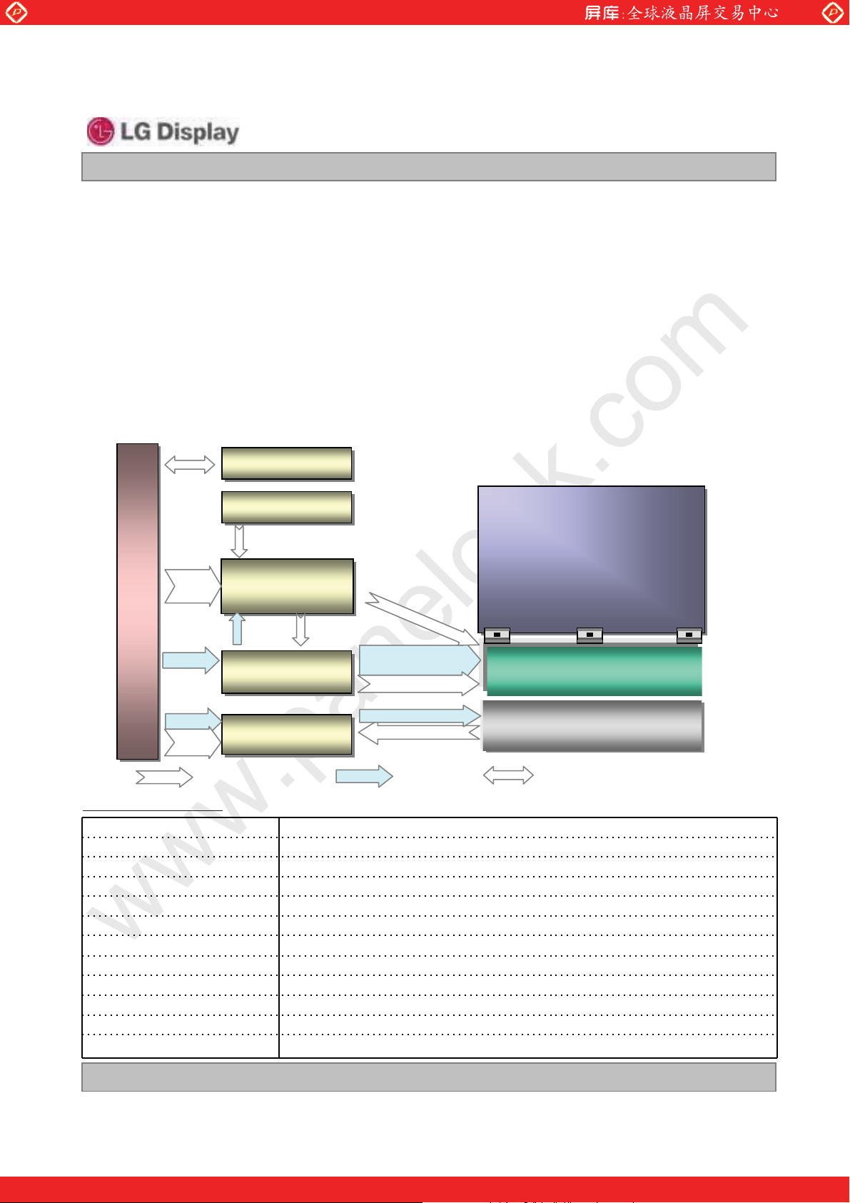
1. General Description
The LP133WH2 is a Color Active Matrix Liquid Crystal Display with an integral LED backlight system. The
matrix employs a-Si Thin Film Transistor as the active element. It is a transmissive type display operating in
the normally white mode. This TFT-LCD has 13.3 inches diagonally measured active display area with HD
resolution (1366 horizontal by 768 vertical pixel array). Each pixel is divided into Red, Green and Blue subpixels or dots which are arranged in vertical stripes. Gray scale or the brightness of the sub-pixel color is
determined with a 6-bit gray scale signal for each dot, thus, presenting a palette of more than 262,144
colors. The LP133WH2 has been designed to apply the interface method that enables low power, high
speed, low EMI. The LP133WH2 is intended to support applications where thin thickness, low power are
critical factors and graphic displays are important. In combination with the vertical arrangement of the subpixels, the LP133WH2 characteristics provide an excellent flat display for office automation products such
as Notebook PC.
www.panelook.com
LP133WH2
Liquid Crystal Display
Product Specification
EEPROM Block
EEPROM Block
for EDID
for EDID
EEPROM Block
EEPROM Block
for Tcon Operating
User connector
for Tcon Operating
1
TFT-LCD Panel
40
Pin
Timing Control
LVDS
1port
VCC
VLED
LED_EN
PWM
Timing Control
(Tcon) Block
(Tcon) Block
DVCC
Power
Block
LED Driver
LED Driver
Block
TCLKs
Power
Block
Block
VGH, VGL, GMA
Control & Data Power
E
PI
DVCC, AVDD
GIP CLKs, DSC
VOUT_LED
FB1~4
768
(HD, GIP, TN)
Source Driver
LED Backlight Ass’y
EDID signal & Power
General Features
Active Screen Size 13.3 inches diagonal
Outline Dimension 306.3(Typ. H) Ý 177.7(Typ. V) Ý 3.6(D, Max.) mm
Pixel Pitch 0.2148 Ý 0.2148 mm
Pixel Format 1366 horiz. by 768 vert. Pixels RGB strip arrangement
Color Depth 6-bit, 262,144 colors
2
Luminance, White 200 cd/m
Power Consumption
Weight 300 g (Max.)
Display Operating Mode Transmissive mode, Normally white
Surface Treatment Glare treatment of the front polarizer
RoHS Compliance Yes
BFR / PVC / As Free Yes for all.
Total 3.0W(Max.) Logic : 0.8 W (Max.@ RGB), B/L : 2.2 W (Max.@ VLED 12V )
( 5P Typ.)
1366
(Bottom)
Ver. 0.0 Aug. 09. 2011
One step solution for LCD / PDP / OLED panel application: Datasheet, inventory and accessory!
4/ 32
www.panelook.com
Page 5
Global LCD Panel Exchange Center
2. Absolute Maximum Ratings
The following are maximum values which, if exceeded, may cause faulty operation or damage to the unit.
www.panelook.com
LP133WH2
Liquid Crystal Display
Product Specification
Table 1. ABSOLUTE MAXIMUM RATINGS
Parameter Symbol
Power Input Voltage
Operating Temperature
Storage Temperature
Operating Ambient Humidity
Storage Humidity
VCC -0.3 4.0 Vdc at 25 r 5qC
TOP 050qC1
HST -20 60 qC1
HOP 10 90 %RH 1
HST 10 90 %RH 1
Values
Units Notes
Min Max
Note : 1. Temperature and relative humidity range are shown in the figure below.
Wet bulb temperature should be 39
Wet Bulb
20
]
30
Temperature [
10
0
qC Max, and no condensation of water.
90% 80%
60
50
40
60%
Humidity[(%)RH]
40%
20%
10%
Storage
Operation
-20
10
20 30 40 50
60 70 800
Dry Bulb Temperature []
Ver. 0.0 Aug. 09. 2011
One step solution for LCD / PDP / OLED panel application: Datasheet, inventory and accessory!
5/ 32
www.panelook.com
Page 6
Global LCD Panel Exchange Center
3. Electrical Specifications
3-1. Electrical Characteristics
The LP133WH2 requires two power inputs. The first logic is employed to power the LCD electronics and to
drive the TFT array and liquid crystal. The second backlight is the input about LED BL with LED Driver.
Table 2. ELECTRICAL CHARACTERISTICS
www.panelook.com
LP133WH2
Liquid Crystal Display
Product Specification
Parameter Symbol
Unit Notes
Min Typ Max
LOGIC :
Values
Power Supply Input Voltage V
Power Supply Input Current RGB I
Power Consumption P
Power Supply Inrush Current I
LVDS Impedance Z
CC 3.0 3.3 3.6 V 1
CC - 220 255 mA 2
CC -0.70.8W2
CC_P - - 1500 mA 3
LVDS 90 100 110
ȳ
BACKLIGHT : ( with LED Driver)
LED Power Input Voltage V
LED Power Input Current I
LED Power Consumption P
LED Power Inrush Current I
LED 7.0 12.0 21.0 V 5
LED - - 190 mA 6
LED -2.2W
LED_P - - 1500 mA 7
PWM Duty Ratio 5 - 100 % 8
PWM Jitter
PWM Impedance Z
-
PWM 20 40 60 kȳ
0-0.2%9
4
PWM Frequency F
PWM High Level Voltage V
PWM Low Level Voltage V
LED_EN Impedance Z
LED_EN High Voltage V
LED_EN Low Voltage V
PWM 200 - 1000 Hz 10
PWM_H
PWM_L
PWM 20 40 60 kȳ
LED_EN_H 3.0 - 5.3 V
LED_EN_L 0-0.3V
3.0 - 5.3 V
0-0.3V
DBC_EN High Voltage 3.0 - 5.3 V
DBC_EN Low Voltage 0 - 0.3 V
Life Time
Ver. 0.0 Aug. 09. 2011
15,000 - - Hrs 12
6/ 32
One step solution for LCD / PDP / OLED panel application: Datasheet, inventory and accessory!
www.panelook.com
Page 7
Global LCD Panel Exchange Center
Note)
1. The measuring position is the connector of LCM and the test conditions are under 25, fv = 60Hz,
Black pattern.
2. The specified Icc current and power consumption are under
the Vcc = 3.3V , 25, fv = 60Hz condition and Mosaic pattern.
3. This Spec. is the max load condition for the cable impedance designing.
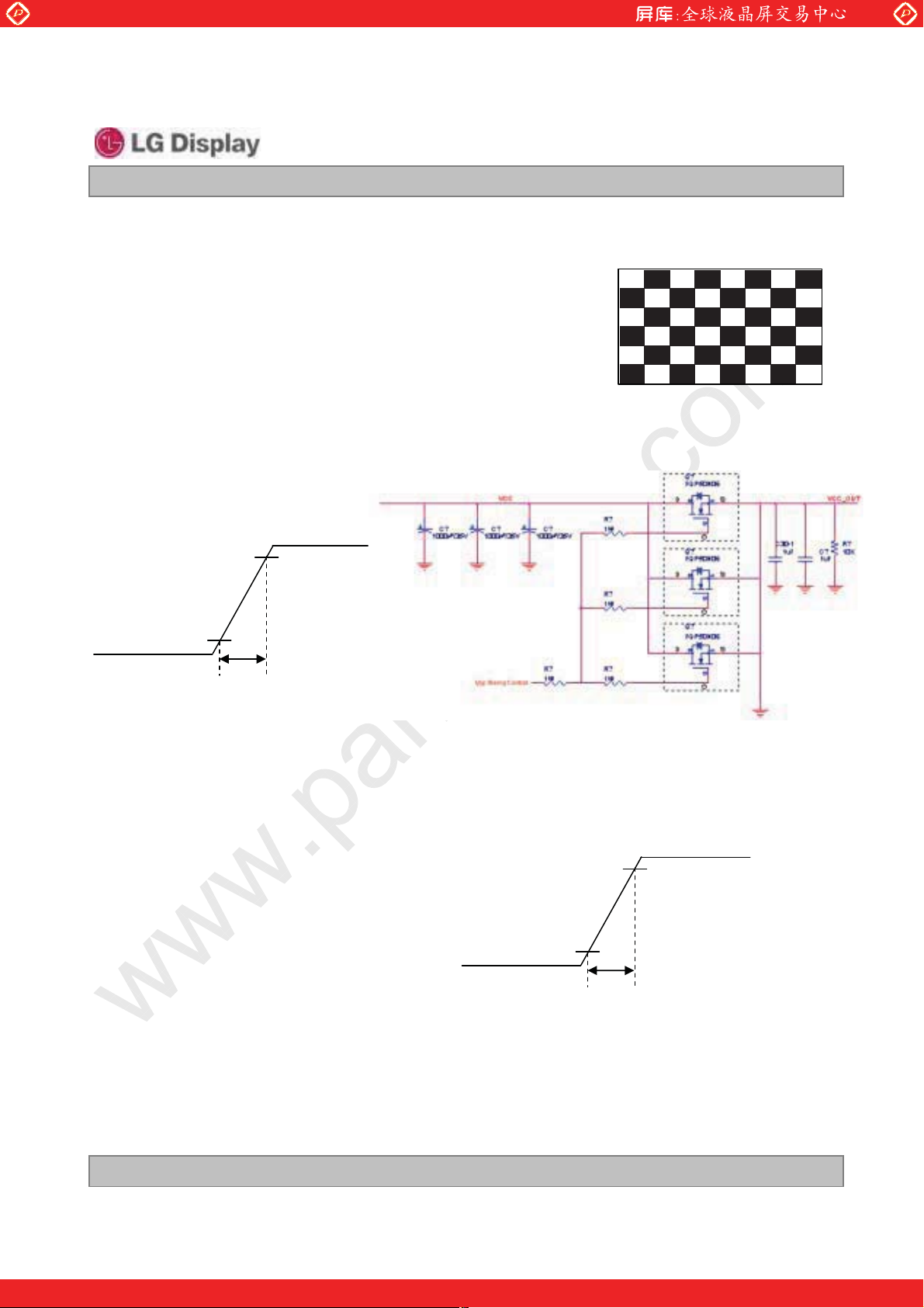
4. The below figures are the measuring Vcc condition and the Vcc control block LGD used.
The Vcc condition is same as the minimum of T1 at Power on sequence.
www.panelook.com
LP133WH2
Liquid Crystal Display
Product Specification
Rising time
Vcc
0V
5. This impedance value is needed for proper display and measured form LVDS Tx to the mating connector.
6. The measuring position is the connector of LCM and the test conditions are under 25.
7. The current and power consumption with LED Driver are under the Vled = 12.0V , 25, Dimming of
Max luminance and White pattern with the normal frame frequency operated(60Hz).
8. The below figures are the measuring Vled condition
and the Vled control block LGD used.
VLED control block is same with Vcc control block.
90%
10%
0.5ms
3.3V
Rising time
LED
V
0V
10%
12.0V
90%
0.1ms
9. The operation of LED Driver below minimum dimming ratio may cause flickering or reliability issue.
10. If Jitter of PWM is bigger than maximum, it may induce flickering.
11. This Spec. is not effective at 100% dimming ratio as an exception because it has DC level equivalent
to 0Hz. In spite of acceptable range as defined, the PWM Frequency should be fixed and stable for
more consistent brightness control at any specific level desired.
12. The life time is determined as the time at which brightness of LCD is 50% compare to that of minimum
value specified in table 7. under general user condition.
Ver. 0.0 Aug. 09. 2011
One step solution for LCD / PDP / OLED panel application: Datasheet, inventory and accessory!
7/ 32
www.panelook.com
Page 8
Global LCD Panel Exchange Center
3-2. Interface Connections
This LCD employs two interface connections, a 40 pin connector used for the module electronics interface and
the other connector used for the integral backlight system.
Table 3. MODULE CONNECTOR PIN CONFIGURATION (CN1)
Pin Symbol Description Notes
1 Test Loop Dell’s Test loop to 34pin
2 VCC LCD Logic and driver power (3.3V Typ.)
3 VCC LCD Logic and driver power (3.3V Typ.)
4 V EEDID DDC Power (3.3V)
5 Bist LCD Panel Self Test Enable
6 Clk EEDID DDC Clock
7 DATA EEDID DDC Data
8 ORX0- Negative LVDS differential data input
9 ORX0+ Positive LVDS differential data input
10 GND LCM Ground
11 ORX1- Negative LVDS differential data input
12 ORX1+ Positive LVDS differential data input
13 GND LCM Ground
14 ORX2- Negative LVDS differential data input
15 ORX2+ Positive LVDS differential data input
16 GND LCM Ground
17 ORXC- Negative LVDS differential clock input
18 ORXC+ Positive LVDS differential clock input
19 GND LCM Ground
20
21
22 GND LCM Ground
23
24
25 GND LCM Ground
26
27
28 GND LCM Ground
29
30
31
32
33
34
35
36
37
38
39
40
NC
NC
NC
NC
NC
NC
NC
NC
GND
GND
GND
Test Loop
PWM System PWM Signal input for dimming
LED_EN
DBC_EN Dynamic Backlight Control enable
VLED LED Backlight Power (7V-21V)
VLED LED Backlight Power (7V-21V)
VLED LED Backlight Power (7V-21V)
No Connection
No Connection
No Connection
No Connection
No Connection
No Connection
No Connection
No Connection
LCM Ground (LED Backlight Ground)
LCM Ground (LED Backlight Ground)
LCM Ground (LED Backlight Ground)
Dell’s Test loop to 1pin
LED Backlight On/Off
www.panelook.com
Product Specification
LP133WH2
Liquid Crystal Display
[Interface Chip]
1. LCD :
LGE, LG5410S (LCD Controller)
Including LVDS Receiver.
2. System : Pin to Pin compatible with LVDS
[Connector]
Hirose KN38-40S-0.5H
UJU IS050-L40B-C10 or equivalent
[Mating Connector]
20453-#40E-## series or equivalent
[Connector pin arrangement]
40
[LCD Module Rear View]
1
Ver. 0.0 Aug. 09. 2011
One step solution for LCD / PDP / OLED panel application: Datasheet, inventory and accessory!
8/ 32
www.panelook.com
Page 9
Global LCD Panel Exchange Center
3-3. LVDS Signal Timing Specifications
3-3-1. DC Specification
www.panelook.com
LP133WH2
Liquid Crystal Display
Product Specification
VDD=1.8V
Description Symbol Min Typ Max Unit Notes
LVDS Differential Voltage |V
LVDS Common mode Voltage V
LVDS Input Voltage Range V
3-3-2. AC Specification
Description Symbol Min Max Unit Notes
LVDS Clock to Data Skew Margin
| 100 - 600 mV -
ID
CM
IN
|VID| /2 1.2 VDD- |VID|/2 V -
0.3 - VDD V -
t
SKEW
t
SKEW
- 400 + 400 ps
- 600 + 600 ps
85MHz > Fclk ˻
65MHz
65MHz > Fclk ˻
25MHz
LVDS Clock to Clock Skew Margin (Even
to Odd)
Maximum deviation
of input clock frequency during SSC
Maximum modulation frequency
of input clock during SSC
Ver. 0.0 Aug. 09. 2011
t
SKEW_EO
F
DEV
F
MOD
-1/7 + 1/7 T
clk
- · 3% -
- 200 KHz -
One step solution for LCD / PDP / OLED panel application: Datasheet, inventory and accessory!
-
9/ 32
www.panelook.com
Page 10
Global LCD Panel Exchange Center
Freq.
www.panelook.com
LP133WH2
Liquid Crystal Display
Product Specification
< Clock skew margin between channel >
F
max
F
center
F
min
3-3-3. Data Format
1) LVDS 1 Port
RCLK+
RA+/-
RB+/-
R3 R2
G4 G3
R1 R0
G2 G1
X
m
tvk
< Spread Spectrum >
G0 R5 R4 R3 R2 R1 R0
B1 B0 G5 G4 G3 G2 G1
m
G0
B1
QGm
kl}
Time
R5 R4
B0 G5
RC+/-
RD+/-
B5 B4
G7 G6
Previous (N-1)th Cycle Next (N+1 )th Cycle
B3 B2
R7 R6
DE VSYNC HSYNC B5 B4 B3 B2
X B7 B6 G7 G6 R7 R6
Current (Nth ) Cycle
DE
VSYNC HSYNC
X
< LVDS Data Format >
Ver. 0.0 Aug. 09. 2011
One step solution for LCD / PDP / OLED panel application: Datasheet, inventory and accessory!
B7 B6
10/ 32
www.panelook.com
Page 11

Global LCD Panel Exchange Center
3-4. Signal Timing Specifications
This is the signal timing required at the input of the User connector. All of the interface signal timing should be
satisfied with the following specifications and specifications of LVDS Tx/Rx for its proper operation.
ITEM Symbol Min. Typ. Max. Unit Note
www.panelook.com
LP133WH2
Liquid Crystal Display
Product Specification
Table 4. TIMING TABLE
DCLK Frequency
Period
Hsync
Vsync
Data
Enable
Width
Width-Active
Period
Width
Width-Active
Horizontal back porch
Horizontal front porch
Vertical back porch
Vertical front porch
3-5. Signal Timing Waveforms
f
CLK
t
HP
t
WH
tw
HA
t
VP
t
WV
tw
VA
t
HBP
t
HFP
t
VBP
t
VFP
High: 0.7VCC
Low: 0.3VCC
-
1464 1476 1516
32 36 56
1366 1366 1366
776 790 792
288
768 768 768
34 38 54
32 36 40
41012
244
70.0
-
MHz
tCLK
tHP
tCLK
tHP
Condition : VCC=3.3V
t
Hsync
t
WH
t
HBP
HP
Date Enable
t
VP
t
WV
Vsync
t
VBP
Date Enable
Ver. 0.0 Aug. 09. 2011
tWHA
tWVA
t
HFP
t
VFP
11/ 32
One step solution for LCD / PDP / OLED panel application: Datasheet, inventory and accessory!
www.panelook.com
Page 12

Global LCD Panel Exchange Center
3-6. Color Input Data Reference
The brightness of each primary color (red,green and blue) is based on the 6-bit gray scale data input for the
color ; the higher the binary input, the brighter the color. The table below provides a reference for color
versus data input.
www.panelook.com
LP133WH2
Liquid Crystal Display
Product Specification
Table 5. COLOR DATA REFERENCE
Input Color Data
Basic
Color
RED
GREEN
BLUE
Color
Black
Red
Green
Blue
Cyan
Magenta
Yellow
White
RED (00)
RED (01)
…
RED (62)
RED (63)
GREEN (00)
GREEN (01)
...
GREEN (62)
GREEN (63)
BLUE (00)
BLUE (01)
…
BLUE (62)
BLUE (63)
RED
MSB LSB
R5 R4 R3 R2 R1 R0 G5 G4 G3 G2 G1 G0 B5 B4 B3 B2 B1 B0
0 0 0 0 0 0 0 0 0 0 0 0 0 0 0 0 0 0
1 1 1 1 1 1 0 0 0 0 0 0 0 0 0 0 0 0
0 0 0 0 0 0 1 1 1 1 1 1 0 0 0 0 0 0
0 0 0 0 0 0 0 0 0 0 0 0 1 1 1 1 1 1
0 0 0 0 0 0 1 1 1 1 1 1 1 1 1 1 1 1
1 1 1 1 1 1 0 0 0 0 0 0 1 1 1 1 1 1
1 1 1 1 1 1 1 1 1 1 1 1 0 0 0 0 0 0
1 1 1 1 1 1 1 1 1 1 1 1 1 1 1 1 1 1
0 0 0 0 0 0 0 0 0 0 0 0 0 0 0 0 0 0
0 0 0 0 0 1 0 0 0 0 0 0 0 0 0 0 0 0
…… …
1 1 1 1 1 0 0 0 0 0 0 0 0 0 0 0 0 0
1 1 1 1 1 1 0 0 0 0 0 0 0 0 0 0 0 0
0 0 0 0 0 0 0 0 0 0 0 0 0 0 0 0 0 0
0 0 0 0 0 0 0 0 0 0 0 1 0 0 0 0 0 0
…… …
0 0 0 0 0 0 1 1 1 1 1 0 0 0 0 0 0 0
0 0 0 0 0 0 1 1 1 1 1 1 0 0 0 0 0 0
0 0 0 0 0 0 0 0 0 0 0 0 0 0 0 0 0 0
0 0 0 0 0 0 0 0 0 0 0 0 0 0 0 0 0 1
…… …
0 0 0 0 0 0 0 0 0 0 0 0 1 1 1 1 1 0
0 0 0 0 0 0 0 0 0 0 0 0 1 1 1 1 1 1
MSB LSB
GREEN
BLUE
MSB LSB
Ver. 0.0 Aug. 09. 2011
One step solution for LCD / PDP / OLED panel application: Datasheet, inventory and accessory!
12/ 32
www.panelook.com
Page 13

Global LCD Panel Exchange Center
3-7. Power Sequence
Power Supply Input
VCC
0V
www.panelook.com
Product Specification
90%
LP133WH2
Liquid Crystal Display
90%
10%10%
Interface Signal, V
i
LVDS
LED on/off control Signal
LED_EN
Dimming control signal
Of LED BL
PWM
LED input Voltage
VLED
Logic
Parameter
T
1
T
2
T
3
T
4
T
5
T
6
T
7
Min. Typ. Max.
0.5 - 10 ms
0-50ms
0-50ms
400 - - ms
200 - - ms
200 - - ms
3-10ms
Value
T
T
1
2
Valid Data
0V
T
5
3.0V
3.0V
0V (Off)
T
9
Valid Data
0V (Low)
T
8
90%
0V
10%
T
12
Table 6. POWER SEQUENCE TABLE
Units
LED
Parameter
T
8
T
9
T
10
T
11
T
12
T
13
T
T
3
7
T
6
T
10
T
11
90%
T
10%
13
T
4
Value
Units
Min. Typ. Max.
10 - - ms
0--ms
0--ms
10 - - ms
0.5 - - ms
0 - 5000 ms
Note)
1. Do not insert the mating cable when system turn on.
2. Valid Data have to meet “3-3. LVDS Signal Timing Specifications”
3. LVDS, LED_EN and PWM need to be on pull-down condition on invalid status.
4. LGD recommend the rising sequence of VLED after the Vcc and valid status of LVDS turn on.
Ver. 0.0 Aug. 09. 2011
One step solution for LCD / PDP / OLED panel application: Datasheet, inventory and accessory!
13/ 32
www.panelook.com
Page 14

Global LCD Panel Exchange Center
www.panelook.com
Liquid Crystal Display
Product Specification
4. Optical Specification
Optical characteristics are determined after the unit has been ‘ON’ and stable for approximately 20 minutes in
a dark environment at 25
at a viewing angle of
FIG. 1 presents additional information concerning the measurement equipment and method.
qC. The values specified are at an approximate distance 50cm from the LCD surface
) and 4 equal to 0q.
FIG. 1 Optical Characteristic Measurement Equipment and Method
LP133WH2
Optical Stage(x,y)
LCD Module
500mm·50mm
Equipment
Table 7. OPTICAL CHARACTERISTICS
Ta=25qC, VCC=3.3V, fV=60Hz, f
Parameter Symbol
Contrast Ratio CR 400 500 - 1
Surface Luminance, white L
Luminance Variation G
Response Time Tr
Color Coordinates
RED RX TBD TBD TBD
GREEN GX TBD TBD TBD
BLUE BX TBD TBD TBD
WHITE WX 0.283 0.313 0.343
Viewing Angle 5
x axis, right()=0q) 4r 40 - - degree
x axis, left ()=180q) 4l 40 - - degree
y axis, up ()=90q)
y axis, down ()=270q) 4d 30 - - degree
Gray Scale 6
Color Gamut C/G - 45 - %
WH 5P
WHITE
R + TrD
RY TBD TBD TBD
GY TBD TBD TBD
BY TBD TBD TBD
WY 0.299 0.329 0.359
4u 10 - - degree
Min Typ Max
170 200 - cd/m
- 1.4 1.6 - 3
-1625ms 4
Values
Units Notes
2
CLK
= 70.0MHz
2
Ver. 0.0 Aug. 09. 2011
One step solution for LCD / PDP / OLED panel application: Datasheet, inventory and accessory!
14/ 32
www.panelook.com
Page 15

Global LCD Panel Exchange Center
www.panelook.com
Liquid Crystal Display
Product Specification
Note)
1. Contrast Ratio(CR) is defined mathematically as
Surface Luminance with all white pixels
Contrast Ratio =
Surface Luminance with all black pixels
2. Surface luminance is the average of 5 point across the LCD surface 50cm from the surface with
all pixels displaying white. For more information see FIG 1.
LWH = Average(L1,L2, … L5)
3. The variation in surface luminance , The panel total variation (G WHITE) is determined by measuring LN
at each test position 1 through 13 and then defined as following numerical formula.
For more information see FIG 2.
LP133WH2
G WHITE =
4. Response time is the time required for the display to transition from white to black (rise time, TrR) and
from black to white (Decay Time, TrD). For additional information see FIG 3.
5. Viewing angle is the angle at which the contrast ratio is greater than 10. The angles are determined
for the horizontal or x axis and the vertical or y axis with respect to the z axis which is normal to the
LCD surface. For more information see FIG 4.
6. Gray scale specification * fV = 60Hz
Maximum(L1,L2, … L13)
Minimum(L1,L2, … L13)
Gray Level Luminance [%] (Typ)
L0 TBD
L7 TBD
L15 TBD
L23 TBD
L31 TBD
L39 TBD
L47 TBD
L55 TBD
L63 TBD
Ver. 0.0 Aug. 09. 2011
One step solution for LCD / PDP / OLED panel application: Datasheet, inventory and accessory!
15/ 32
www.panelook.com
Page 16

Global LCD Panel Exchange Center
FIG. 2 Luminance
<Measuring point for Average Luminance & measuring point for Luminance variation>
www.panelook.com
Product Specification
H
A
LP133WH2
Liquid Crystal Display
D
L6
C
L2
B
V
L9
L4 L5
L11 L13
L7
L3
L1
Center Point
L12
L8
L10
H,V : ACTIVE AREA
A : H/4 mm
B : V/4 mm
C : 10 mm
D : 10 mm
POINTS : 13 POINTS
FIG. 3 Response Time
The response time is defined as the following figure and shall be measured by switching the input signal
for “black” and “white”.
Tr
Tr
R
D
%
100
90
Optical
Response
10
0
white
white
black
FIG. 4 Viewing angle
I
= 180
q
<Dimension of viewing angle range>
,
Left
Normal
Eye
Y
I
= 90q, Up
T
I
q
,
Right
I
= 270
q
Down
,
Ver. 0.0 Aug. 09. 2011
I
= 0
One step solution for LCD / PDP / OLED panel application: Datasheet, inventory and accessory!
16/ 32
www.panelook.com
Page 17

Global LCD Panel Exchange Center
5. Mechanical Characteristics
The contents provide general mechanical characteristics for the model LP133WH2.
In addition the figures in the next page are detailed mechanical drawing of the LCD.
www.panelook.com
LP133WH2
Liquid Crystal Display
Product Specification
Horizontal 306.3 r 0.50mm
Outline Dimension
Bezel Area
Active Display Area
Weight 300 g (Max.)
Surface Treatment Glare treatment of the front polarizer
Vertical 177.7 r 0.50mm
Thickness 3.6 mm (Max.)
Horizontal 297.42 mm
Vertical 168.57 mm
Horizontal 293.42mm
Vertical 164.97 mm
Ver. 0.0 Aug. 09. 2011
One step solution for LCD / PDP / OLED panel application: Datasheet, inventory and accessory!
17/ 32
www.panelook.com
Page 18

Global LCD Panel Exchange Center
www.panelook.com
LP133WH2
Liquid Crystal Display
Product Specification
<FRONT VIEW>
Note) Unit:[mm], General tolerance:
r 0.5mm
Ver. 0.0 Aug. 09. 2011
One step solution for LCD / PDP / OLED panel application: Datasheet, inventory and accessory!
18/ 32
www.panelook.com
Page 19

Global LCD Panel Exchange Center
www.panelook.com
LP133WH2
Liquid Crystal Display
Product Specification
<REAR VIEW>
Note) Unit:[mm], General tolerance:
r 0.5mm
Ver. 0.0 Aug. 09. 2011
One step solution for LCD / PDP / OLED panel application: Datasheet, inventory and accessory!
19/ 32
www.panelook.com
Page 20

Global LCD Panel Exchange Center
[ DETAIL INFORMATION OF PPID LABEL AND REVISION CODE ]
* Manufacturing Location
www.panelook.com
LP133WH2
Liquid Crystal Display
Product Specification
* PPID Label Revision
* PPID Label Revision :
It is subject to change with Dell event. Please refer to the below table for detail.
Classification No Change 1st Revision 2nd Revision … 9th Revision …
SST(WS) X00 X01 X02 … A09 …
PT(ES) X10 X11 X12 … A19 …
ST(CS) X20 X21 X22 … A29 …
XB(MP) A00 A01 A02 … A09 …
Manufacturing Location
KR Korea
CN China
Ver. 0.0 Aug. 09. 2011
One step solution for LCD / PDP / OLED panel application: Datasheet, inventory and accessory!
20/ 32
www.panelook.com
Page 21

Global LCD Panel Exchange Center
LGD Proposal for system cover design.(Appendix)
www.panelook.com
LP133WH2
Liquid Crystal Display
Product Specification
1
Gap check for securing the enough gap between LCM
and System cover.
Max Thickness
Sponge
LCM reflector side
System Cover
A Boundary Line
1.Rear side of LCM is sensitive against external stress,and previous check
about interference is highly needed.
Define
2.In case there is something from system cover comes into the boundary
above,mechanical interference may cause the FOS defects.
(Eg:Ripple,White spot..)
2 Check if antenna cable is sufficiently apart from T-CON of LCD Module.
Define
NO GOOD
GOOD
1.If system antenna is overlapped with T-CON,it might be cause the noise.
Ver. 0.0 Aug. 09. 2011
21/ 32
One step solution for LCD / PDP / OLED panel application: Datasheet, inventory and accessory!
www.panelook.com
Page 22

Global LCD Panel Exchange Center
LGD Proposal for system cover design.
www.panelook.com
LP133WH2
Liquid Crystal Display
Product Specification
3
Plate Bottom
Define
Gap check for securing the enough gap between LCM
and System hinge.
LCM reflector side
Source PCB
Hinge
GAP:Min2.0mm
(“I” TYPE)
1.At least 2.0mm of gap needs to be secured to prevent the shock
LED
(“L” TYPE)
related defects.
2.”L” type of hinge is recommended than “I” type under shock test.
4
Checking the path of the System wire.
#3
Good
Ok
Bad
1.COF area needs to be handled with care.
2.GOOD ÎWire path design to system side.
Define
OKÎ Wire path is located between COFs.
BADÎWire path overlapped with COF area.
Ver. 0.0 Aug. 09. 2011
#2
#1
22/ 32
One step solution for LCD / PDP / OLED panel application: Datasheet, inventory and accessory!
www.panelook.com
Page 23

Global LCD Panel Exchange Center
LGD Proposal for system cover design.
5 Using a bracket on the top of LCM is not recommended.
bracket
www.panelook.com
LP133WH2
Liquid Crystal Display
Product Specification
With bracket Without bracket
1.Condition without bracket is good for mechanical noise,and can minimize
the light leakage from deformation of bracket.
Define
2.The results shows that there is no difference between the condition
with or without bracket.
6 Securing additional gap on CNT area..
A
A~A-1
cut
System cover inner side.
User connector
area.
A-1
User connector
Cable pathway.
FPC:Flexible Printed Circuit.
1.CNT area is specially sensitive against external stress,and additional
Define
gap by cutting on system cover will be helpful on removing the Ripple.
2.Using a thinner CNT will be better. (eg: FPC type)
Ver. 0.0 Aug. 09. 2011
One step solution for LCD / PDP / OLED panel application: Datasheet, inventory and accessory!
23/ 32
www.panelook.com
Page 24

Global LCD Panel Exchange Center
6. Reliability
Environment test condition
No. Test Item Conditions
1 High temperature storage test Ta= 60qC, 240h
2 Low temperature storage test Ta= -20qC, 240h
3 High temperature operation test Ta= 50qC, 50%RH, 240h
4 Low temperature operation test Ta= 0qC, 240h
www.panelook.com
LP133WH2
Liquid Crystal Display
Product Specification
5 Vibration test (non-operating) Sine wave, 5 ~ 150Hz, 1.5G, 0.37oct/min
3 axis, 30min/axis
6 Shock test (non-operating) - No functional or cosmetic defects following a shock
to all 6 sides delivering at least 180 G in a half sine
pulse no longer than 2 ms to the display module
- No functional defects following a shock delivering
at least 200 g in a half sine pulse no longer than 2
ms to each of 6 sides. Each of the 6 sides will be
shock tested with one each display, for a total of 6
displays
7 Altitude operating
storage / shipment
{ Result Evaluation Criteria }
There should be no change which might affect the practical display function when the display quality
test is conducted under normal operating condition.
0 ~ 10,000 feet (3,048m) 24Hr
0 ~ 40,000 feet (12,192m) 24Hr
Ver. 0.0 Aug. 09. 2011
One step solution for LCD / PDP / OLED panel application: Datasheet, inventory and accessory!
24/ 32
www.panelook.com
Page 25

Global LCD Panel Exchange Center
7. International Standards
7-1. Safety
a) UL 60950-1, Underwriters Laboratories Inc.
Information Technology Equipment - Safety - Part 1 : General Requirements.
b) CAN/CSA C22.2 No.60950-1-07, Canadian Standards Association.
Information Technology Equipment - Safety - Part 1 : General Requirements.
c) EN 60950-1, European Committee for Electrotechnical Standardization (CENELEC).
Information Technology Equipment - Safety - Part 1 : General Requirements.
d) IEC 60950-1, The International Electrotechnical Commission (IEC).
Information Technology Equipment - Safety - Part 1 : General Requirements.
www.panelook.com
LP133WH2
Liquid Crystal Display
Product Specification
Ver. 0.0 Aug. 09. 2011
One step solution for LCD / PDP / OLED panel application: Datasheet, inventory and accessory!
25/ 32
www.panelook.com
Page 26

Global LCD Panel Exchange Center
8. Packing
8-1. Designation of Lot Mark
a) Lot Mark
ABCDEFGHI JKLM
A,B,C : SIZE(INCH) D : YEAR
E : MONTH F ~ M : SERIAL NO.
www.panelook.com
LP133WH2
Liquid Crystal Display
Product Specification
Note
1. YEAR
Year
Mark
CBA
2014E2015
D
201320122011
2016G2017H2018J2019
F
2. MONTH
Month
Mark
Apr5May
4
Jun
6
Jul8Aug9Sep
7
b) Location of Lot Mark
Serial No. is printed on the label. The label is attached to the backside of the LCD module.
This is subject to change without prior notice.
8-2. Packing Form
a) Package quantity in one box : 20pcs
b) Box Size : 422mm X 340mm X 257mm
2020
K
Oct
A
Nov
B
DecMarFebJan
C321
Ver. 0.0 Aug. 09. 2011
One step solution for LCD / PDP / OLED panel application: Datasheet, inventory and accessory!
26/ 32
www.panelook.com
Page 27

Global LCD Panel Exchange Center
9. PRECAUTIONS
Please pay attention to the followings when you use this TFT LCD module.
9-1. MOUNTING PRECAUTIONS
(1) You must mount a module using holes arranged in four corners or four sides.
(2) You should consider the mounting structure so that uneven force (ex. Twisted stress) is not applied to the
module. And the case on which a module is mounted should have sufficient strength so that external
force is not transmitted directly to the module.
(3) Please attach the surface transparent protective plate to the surface in order to protect the polarizer.
Transparent protective plate should have sufficient strength in order to the resist external force.
(4) You should adopt radiation structure to satisfy the temperature specification.
(5) Acetic acid type and chlorine type materials for the cover case are not desirable because the former
generates corrosive gas of attacking the polarizer at high temperature and the latter causes circuit break
by electro-chemical reaction.
(6) Do not touch, push or rub the exposed polarizers with glass, tweezers or anything harder than HB
pencil lead. And please do not rub with dust clothes with chemical treatment.
Do not touch the surface of polarizer for bare hand or greasy cloth.(Some cosmetics are detrimental
to the polarizer.)
(7) When the surface becomes dusty, please wipe gently with absorbent cotton or other soft materials like
chamois soaks with petroleum benzene. Normal-hexane is recommended for cleaning the adhesives
used to attach front / rear polarizers. Do not use acetone, toluene and alcohol because they cause
chemical damage to the polarizer.
(8) Wipe off saliva or water drops as soon as possible. Their long time contact with polarizer causes
deformations and color fading.
(9) Do not open the case because inside circuits do not have sufficient strength.
(10) When handling the LCD module, it needs to handle with care not to give mechanical stress to the PCB
and Mounting Hole area.”
www.panelook.com
LP133WH2
Liquid Crystal Display
Product Specification
9-2. OPERATING PRECAUTIONS
(1) The spike noise causes the mis-operation of circuits. It should be lower than following voltage :
V=· 200mV(Over and under shoot voltage)
(2) Response time depends on the temperature.(In lower temperature, it becomes longer.)
(3) Brightness depends on the temperature. (In lower temperature, it becomes lower.)
And in lower temperature, response time(required time that brightness is stable after turned on) becomes
longer.
(4) Be careful for condensation at sudden temperature change. Condensation makes damage to polarizer or
electrical contacted parts. And after fading condensation, smear or spot will occur.
(5) When fixed patterns are displayed for a long time, remnant image is likely to occur.
(6) Module has high frequency circuits. Sufficient suppression to the electromagnetic interference shall be
done by system manufacturers. Grounding and shielding methods may be important to minimized the
interference.
Ver. 0.0 Aug. 09. 2011
27/ 32
One step solution for LCD / PDP / OLED panel application: Datasheet, inventory and accessory!
www.panelook.com
Page 28

Global LCD Panel Exchange Center
9-3. ELECTROSTATIC DISCHARGE CONTROL
Since a module is composed of electronic circuits, it is not strong to electrostatic discharge. Make certain that
treatment persons are connected to ground through wrist band etc. And don’t touch interface pin directly.
9-4. PRECAUTIONS FOR STRONG LIGHT EXPOSURE
Strong light exposure causes degradation of polarizer and color filter.
9-5. STORAGE
When storing modules as spares for a long time, the following precautions are necessary.
www.panelook.com
LP133WH2
Liquid Crystal Display
Product Specification
(1) Store them in a dark place. Do not expose the module to sunlight or fluorescent light. Keep the
temperature between 5qC and 35qC at normal humidity.
(2) The polarizer surface should not come in contact with any other object.
It is recommended that they be stored in the container in which they were shipped.
9-6. HANDLING PRECAUTIONS FOR PROTECTION FILM
(1) When the protection film is peeled off, static electricity is generated between the film and polarizer.
This should be peeled off slowly and carefully by people who are electrically grounded and with well
ion-blown equipment or in such a condition, etc.
(2) The protection film is attached to the polarizer with a small amount of glue. If some stress is applied
to rub the protection film against the polarizer during the time you peel off the film, the glue is apt to
remain on the polarizer.
Please carefully peel off the protection film without rubbing it against the polarizer.
(3) When the module with protection film attached is stored for a long time, sometimes there remains a
very small amount of glue still on the polarizer after the protection film is peeled off.
(4) You can remove the glue easily. When the glue remains on the polarizer surface or its vestige is
recognized, please wipe them off with absorbent cotton waste or other soft material like chamois
soaked with normal-hexane.
Ver. 0.0 Aug. 09. 2011
One step solution for LCD / PDP / OLED panel application: Datasheet, inventory and accessory!
28/ 32
www.panelook.com
Page 29

Global LCD Panel Exchange Center
t
e
APPENDIX A. Enhanced Extended Display Identification Data (EEDIDTM) 1/3
Byte
Byte
(D ec)
(He x)
0
1
2
3
4
HeaderVendor / ProductDisplayVendor / Produc
5
6
7
8
9
10
11
12
13
14
15
16
17
18
19
20
21
22
23
24
25
26
27
28
29
30
31
32
33
34
35
36
37
Establish
38
39
40
41
42
43
44
45
46
47
48
49
Standard Timing ID
50
51
52
53
He ader
00
He ader
01
He ader
02
He ader
03
He ader
04
He ader
05
He ader
06
He ader
07
ID M anuf act ure Na m e L GD
08
ID M anufactu re Name
09
ID P ro duct C ode 035 5h
0A
( H ex. LS B first )
0B
ID Serial N o. - Optional ( "00 h" I f not us ed , Numb er O nly and L SB First)
0C
ID Serial N o. - Optional ( "00 h" I f not us ed , Numb er O nly and L SB First)
0D
ID Serial N o. - Optional ( "00 h" I f not us ed , Numb er O nly and L SB First)
0E
ID Serial N o. - Optional ( "00 h" I f not us ed , Numb er O nly and L SB First)
0F
W e ek of M a nu fac tu re - O pt in al 0 0 we eks
10
Ye ar of M anu fa ctu re 201 1 ye ars
11
ED ID structure ve rsion # = 1
12
EDID revision # = 4
13
Vid eo inpu t Defin ition = Inp ut is a Digital V ideo signal Interface , Colo B it Dep th : 6 Bits per P rimary Colo r ,
14
Digital Video Interface Standard Supported: Digital Interface is not defined
Horizontal Screen Size (Rounded cm) = 29 cm
15
Vertical Screen Size (Ro unded cm ) = 16 cm
16
Display Transfer Characteristic (Gamma) = (gamma*100)-100 = Example:(2.2*100)-100=120 = 2.2 Gamma
17
Feature Support [ Display Power Management(DPM ) : Standby Mode is not supported, Suspend Mode is not
supp orted , Ac tive O ff = Ve ry Lo w Pow er is not supp orted ,Sup po rtted C olor E ncod ing F orm ats : RG B 4:4 :4
18
,Other Feature Support Flags : No_sRGB, Preferred Timing Mode, No_Display is continuous frequency
(Multi-mode_Base EDID and Extension Block).]
Red/Green Low Bits (RxRy/GxGy)
19
Blu e/W hite Low Bits (B xB y/W xW y)
1A
Red X Rx = 00
1B
Re d Y R y = 00
1C
Green X Gx = 00
1D
Green Y Gy = 00
1E
Bl ue X B x = 00
1F
Bl ue Y B y = 00
20
White X Wx = 0.313
21
White Y Wy = 0.329
22
Established timing 1 ( Optional_00h if not used)
23
Established timing 2 ( Optional_00h if not used)
24
M anufac turer's timin gs ( Optional_ 00h if not used)
25
Stand ard timing ID 1 ( O ptional_ 01h if no t used )
26
Stand ard timing ID 1 ( O ptional_ 01h if no t used )
27
Stand ard timing ID 2 ( O ptional_ 01h if no t used )
28
Stand ard timing ID 2 ( O ptional_ 01h if no t used )
29
Stand ard timing ID 3 ( O ptional_ 01h if no t used )
2A
Stand ard timing ID 3 ( O ptional_ 01h if no t used )
2B
Stand ard timing ID 4 ( O ptional_ 01h if no t used )
2C
Stand ard timing ID 4 ( O ptional_ 01h if no t used )
2D
Stand ard timing ID 5 ( O ptional_ 01h if no t used )
2E
Stand ard timing ID 5 ( O ptional_ 01h if no t used )
2F
Stand ard timing ID 6 ( O ptional_ 01h if no t used )
30
Stand ard timing ID 6 ( O ptional_ 01h if no t used )
31
Stand ard timing ID 7 ( O ptional_ 01h if no t used )
32
Stand ard timing ID 7 ( O ptional_ 01h if no t used )
33
Stand ard timing ID 8 ( O ptional_ 01h if no t used )
34
Stand ard timing ID 8 ( O ptional_ 01h if no t used )
35
www.panelook.com
Product Specification
Field Name and Comments
LP133WH2
Liquid Crystal Display
Value
(H ex)
00
FF
FF
FF
FF
FF
FF
00
30
E4
55
03
00
00
00
00
00
15
01
04
90
1D
10
78
02
00
05
00
00
00
00
00
00
50
54
00
00
00
01
01
01
01
01
01
01
01
01
01
01
01
01
01
01
01
Value
(B in)
00000000
11111111
11111111
11111111
11111111
11111111
11111111
00000000
00110000
11100100
01010101
00000011
00000000
00000000
00000000
00000000
00000000
00010101
00000001
00000100
10010000
00011101
00010000
01111000
00000010
00000000
00000101
00000000
00000000
00000000
00000000
00000000
00000000
01010000
01010100
00000000
00000000
00000000
00000001
00000001
00000001
00000001
00000001
00000001
00000001
00000001
00000001
00000001
00000001
00000001
00000001
00000001
00000001
00000001
Ver. 0.0 Aug. 09. 2011
One step solution for LCD / PDP / OLED panel application: Datasheet, inventory and accessory!
29/ 32
www.panelook.com
Page 30

Global LCD Panel Exchange Center
APPENDIX A. Enhanced Extended Display Identification Data (EEDIDTM) 2/3
Byte
Byte
(Dec)
(He x)
54
55
56
57
58
59
60
61
62
63
64
65
66
Tim ing D escriptor #1Tim ing D escriptor #2Timing D escriptor #3
67
68
69
70
71
72
73
74
75
76
77
78
79
80
81
82
83
84
85
86
87
88
89
90
91
92
93
94
95
96
97
98
99
100
101
102
103
104
105
106
107
Pi xe l C loc k/ 10 ,0 00 (LS B) 7 0 M Hz @ 60Hz
36
Pi xe l C loc k/ 10 ,0 00 (MS B )
37
Ho ri zo nta l Active (H A) (lo we r 8 b its) 13 66 Pixe ls
38
Ho ri zo nta l Blan ki ng (H B ) (lo we r 8 b its) 1 1 0 Pix els
39
Horizontal Active / Horizontal Blanking(HA HB) (upper 4:4bits)
3A
Ve rtical A vtiv e ( V A ) 768 Lines
3B
Ve rtical B lank ing (V B ) ( DE B la nking ty p.for D E o nly panels) 2 2 Lin es
3C
Ve rtical A ctive / Ve rtical B lanking (V A V B) (u ppe r 4:4b its)
3D
Ho rizonta l Front P orch in pixels (H F) (lower 8 bits)3 6 Pixels
3E
Ho ri zo nta l Sync P uls e W id th in pix el s ( HS) (lo w er 8 bits) 36 Pi xels
3F
Ve rtical Front Porc h in lines (VF ) (lower 4 bits) : Vertical Sync Pluse Wid th in lines (VS ) (lower 4 bits)
40
Ho rizonta l Front P orch/ Sync Pulse W idth/ Ver tical Fro nt Po rch / Sync Pulse W idth (uppe r 2b its)
41
Ho ri zo nta l Vedio Im a ge Siz e (mm ) (lo we r 8 b its) 29 3 mm
42
Ve rtical V ed io Im ag e S ize (m m) (lowe r 8 b its) 16 5 mm
43
Ho rizonta l Image Size / V ertical Imag e Size (upp er 4 bits)
44
Ho rizonta l Bo rd er = 0 (Z ero fo r N oteb ook LCD)
45
Vertical Border = 0 (Zero for Notebook LCD)
46
No n-Interlac e, N ormal display, no ste reo, Digital Sep arate [ Vsync_ NE G, Hs ync_P OS (o utside of V-sync ) ]
47
Pi xe l C loc k/ 10 ,0 00 (LS B) 4 6. 7 M H z @ 40.1Hz
48
Pi xe l C loc k/ 10 ,0 00 (MS B )
49
Ho ri zo nta l Active (H A) (lo we r 8 b its) 13 66 Pixe ls
4A
Ho ri zo nta l Blan ki ng (H B ) (lo we r 8 b its) 1 1 0 Pix els
4B
Horizontal Active / Horizontal Blanking(HA HB) (upper 4:4bits)
4C
Ve rtical A vtiv e ( V A ) 768 Lines
4D
Ve rtical B lank ing (V B ) ( DE B la nking ty p.for D E o nly panels) 2 2 Lin es
4E
Ve rtical A ctive / Ve rtical B lanking (V A V B) (u ppe r 4:4b its)
4F
Ho rizonta l Front P orch in pixels (H F) (lower 8 bits)3 6 Pixels
50
Ho ri zo nta l Sync P uls e W id th in pix el s ( HS) (lo w er 8 bits) 36 Pi xels
51
Ve rtical Front Porc h in lines (VF ) (lower 4 bits) : Vertical Sync Pluse Wid th in lines (VS ) (lower 4 bits)
52
Ho rizonta l Front P orch/ Sync Pulse W idth/ Ver tical Fro nt Po rch / Sync Pulse W idth (uppe r 2b its)
53
Ho ri zo nta l Vedio Im a ge Siz e (mm ) (lo we r 8 b its) 29 3 mm
54
Ve rtical V ed io Im ag e S ize (m m) (lowe r 8 b its) 16 5 mm
55
Ho rizonta l Image Size / V ertical Imag e Size (upp er 4 bits)
56
Ho rizonta l Bo rd er = 0 (Z ero fo r N oteb ook LCD)
57
Vertical Border = 0 (Zero for Notebook LCD)
58
No n-Interlac e, N ormal display, no ste reo, Digital Sep arate [ Vsync_ NE G, Hs ync_P OS (o utside of V-sync ) ]
59
Flag
5A
Flag
5B
Flag
5C
Da ta T ype T ag : A lphanu meric D ata S tring (AS CII S tring)
5D
Flag
5E
De ll P/N 1st C haracter = Y
5F
De ll P/N 2 nd C h ara cter = 3
60
De ll P/N 3 rd C ha rac ter = 8
61
De ll P/N 4th C haracter = C
62
De ll P/N 5th C haracter = 6
63
ED ID R ev is ion B ui ld N am e = S SI (WS ) , Re vi sion # = X 00
64
M an ufa cture r P/N = 1
65
M an ufa cture r P/N = 3
66
M an ufa cture r P/N = 3
67
M an ufa cture r P/N = W
68
M an ufa cture r P/N = H
69
M an ufa cture r P/N = 2
6A
Manufacturer P/N (If < 13 char, then terminate with ASCĊ code 0Ah,set remaining char = 20h)
6B
www.panelook.com
Product Specification
Field Name and Comments
LP133WH2
Liquid Crystal Display
Value
(Hex)
58
1B
56
6E
50
00
16
30
24
24
48
00
25
A5
10
00
00
1A
3E
12
56
6E
50
00
16
30
24
24
48
00
25
A5
10
00
00
1A
00
00
00
FE
00
59
33
38
43
36
00
31
33
33
57
48
32
0A
Value
(B in)
01011000
00011011
01010110
01101110
01010000
00000000
00010110
00110000
00100100
00100100
01001000
00000000
00100101
10100101
00010000
00000000
00000000
00011010
00111110
00010010
01010110
01101110
01010000
00000000
00010110
00110000
00100100
00100100
01001000
00000000
00100101
10100101
00010000
00000000
00000000
00011010
00000000
00000000
00000000
11111110
00000000
01011001
00110011
00111000
01000011
00110110
00000000
00110001
00110011
00110011
01010111
01001000
00110010
00001010
Ver. 0.0 Aug. 09. 2011
One step solution for LCD / PDP / OLED panel application: Datasheet, inventory and accessory!
30/ 32
www.panelook.com
Page 31

Global LCD Panel Exchange Center
m
APPENDIX A. Enhanced Extended Display Identification Data (EEDIDTM) 3/3
Byte
Byte
(Dec)
(Hex)
Timing Descriptor #4
108
109
110
111
112
113
114
115
116
117
118
119
120
121
122
123
124
125
Flag
6C
Flag
6D
Flag
6E
Data T ype Tag : Descriptor D efined by m anufac turer
6F
Flag
70
Color M anagement [ No +2 FRC S upp ort, True Color D epth : 6 bit ]
71
Panel T ype [ WLED ] , Configuration [ Sing le light b ar ], N umb er La mp or LED Light Bar [ one ]
72
Frame Rate Details [ Minimum Frame Rate : 40Hz, Maximum Frame Rate : 65Hz , Tcon provides native
73
Intel No D RRS / sD RRS supp ort ]
Contro ller Interfac e and Maximum Luminance [ PW M type , 200 nit ]
74
Front S urface / Po larizer [ G lossy/True-life, No T ransflective ] , Pixel Structure [ R GB v-strip e ]
75
Multi-Media Features [ Color Management : NTSC, Dynamic Backlight Control : Type 1 ]
76
Multi-Media Features [ Motion Blur : No support , Active Gamma Control : No support ]
77
Special Featur es [ W ireless E nhancement Hardware : N o s upport , In-Ce ll Scanner : No support ]
78
Special Featur es [ Nu mbe r of LVDS channe ls or eD P lanes : one , Overdrive : No ,Interface : LVD S , In-Cell
79
Touch Supp ort : No ]
Special Featur es [ BIST Supp ort : ye s , Electronic P rivacy : No electronic privacy hard ware support , 3-D
7A
Support : No ]
(If<13 char--> 0Ah, then te rminate with AS CĊ code 0Ah,set remaining char = 20h)
7B
(If<13 char--> 0Ah, then te rminate with AS CĊ code 0Ah,set remaining char = 20h)
7C
(If<13 char--> 0Ah, then te rminate with AS CĊ code 0Ah,set remaining char = 20h)
7D
www.panelook.com
Product Specification
Field Name and Comments
LP133WH2
Liquid Crystal Display
Value
(Hex)
00
00
00
00
00
00
41
01
94
01
10
00
00
01
01
0A
20
20
Value
(Bin)
00000000
00000000
00000000
00000000
00000000
00000000
01000001
00000001
10010100
00000001
00010000
00000000
00000000
00000001
00000001
00001010
00100000
00100000
126
127
Checksu
Extension flag (# of optional 128 panel ID extension block to follow, Typ = 0)
7E
Check Sum ( The 1-byte sum of all 128 bytes in this pan el ID block sh all = 0)
7F
00
31
00000000
00110001
Ver. 0.0 Aug. 09. 2011
One step solution for LCD / PDP / OLED panel application: Datasheet, inventory and accessory!
31/ 32
www.panelook.com
 Loading...