

Page 1
CHENHUAN CH ( LGEND R&D.R&D SUPPORT GROUP / officer
* The date(Create Date, Approved Date, Check Date) is based on Korean standard time(GMT+9)
Created Date 2009-01-06 14:17 (Korea Time)
Requested by
최찬용 ( DD전략구매모듈그룹 / 대리 , 82-054-470-2891 )
Subject [Aproval Formal] EAJ60134701_LGD(LM270WF1-TLB1)
Biz Map Procure Materials and Services > Develop Procurement Strategy
DD구매팀 > 05.DD개발구매그룹 > 승인원
EDMS Attributes
Team Map
Doc Type Approval Retention 5 Year
Info Type
Security Grade Internal use (Only) Doc Language Korean
Component Development Information
Component Development Information
Component Development InformationComponent Development Information
Model : W2753V-PFV, M2794DP
Approval type : New (●) Limit () Revision () 4M ()
HSMS (RoHS) : Complete (●) Limit Approval () Warranty Approval ()
Reliability test : Needless ( ) Need (Test Report No: ● )
Class Name : LCD,Module-TFT
Part Number : EAJ60134701
Maker : LG Display
Specification : LM270WF1-TLB1_ZBD FULLHD 27.0INCH 1920X1080 400CD COLOR 92% 16/9 1000:1
P5, R/T:5ms, V/A:170(H)/160(V)
Key part list : T-con:Renasas(Bliss),S-IC:Magna,G-IC:Lusem,Lamp:Wooree ETI,B/L Assy:Heesung,POL:Optimax
Prism(1ea)+Diffuser(1ea), W/O INVETER
Development History : LGD 16:9 27"W(BDI) New module development
★Safety Standard Parts [안전규격부품 List]
Power Cord, Power Plug, X / Y-Capacitor, Power Switch, Fuse, SMPS Trans, Stand-By Trans, Photo coupler,
Insulation (절연) Resistor, Discharge (방전)Resistor, Fusing Resistor, FBT,CPT, CPT Socket, DY, D-Coil,
Line Filter, PCB Material, Front / Back-cover Material, Relay(1-2차간), Varistor, Adaptor, PSU(Power supply unit)
★EMC Standard Parts [전파규격 부품 List]
Power Plug, Line Filter, X-Capacitor, Y-Capacitor, SMPS Trans, Tuner, Saw-Filter, Shield Case, Oscillator, Pattern Change
★Green [유해물질 확인사항]
This item must meet the standards of LG Electronics for six major substances as designated by RoHS for control.
Approval Type Status Approved Date Approved by / Comment
Agree Approved 2009-02-12 10:36
1 )
Comment :
OK
ZULIQIANG ZLQ ( LGEND R&D.R&D SUPPORT GROUP /
Agree Approved 2009-02-13 18:02
Agree Approved 2009-02-16 09:16
Agree Approved 2009-02-16 10:14
manager a )
Comment :
손경조
이상욱
( DD
Comment :
( DD
Comment :
OK
규격그룹 / 선임연구원
확인합니다.
규격그룹 / 수석연구원
확인합니다
)
)
차상호 ( DD규격그룹 / 책임연구원 )
Approval Line
Agree Approved 2009-02-16 13:10
Comment :
확인합니다
.
이문희 ( MNT기구개발그룹 / 책임연구원 )
Agree Approved 2009-02-16 13:45
Comment :
확인 합니다.
이재선 ( Monitor기구개발그룹 / 선임연구원 )
Agree Approved 2009-02-16 15:14
Comment :
확인함. M2794 기구담당자는 김병근주임입니다.
김명욱 ( LGEND R&D.R&D 1 GROUP / 책임연구원 )
Agree Approved 2009-02-16 18:34
Comment :
ok
장원기 ( MNT회로개발그룹 / 책임연구원 )
Agree Approved 2009-02-16 19:13
Comment :
확인합니다.
한상석 ( Monitor회로개발그룹 / 선임연구원 )
Agree Approved 2009-02-17 07:45
Comment :
확인합니다.
Approval Approved 2009-02-18 09:58 정동원
전략구매모듈그룹 / 차장
( DD
)
Page 2
CC
EDMS Doc Link
Attached Local Files
Comment :
확인합니다.
박동호 ( BS Module전략Sourcing그룹 / 부장 )
Approval Approved 2009-02-18 11:53
ok
윤시열
( MNT R&D
기획그룹 / 책임연구원
Comment :
)
정동원 ( DD전략구매모듈그룹 / 차장 )
송재학 ( BS품질보증그룹 / 차장 )
손상익 ( DD전략구매모듈그룹 / 과장 )
이기형 ( MNT R&D기획그룹 / 선임연구원 )
최찬용
전략구매모듈그룹 / 대리
( DD
)
신동석 ( Display부품품질보증그룹 / 대리 )
허희준 ( MNT R&D기획그룹 / 주임연구원 )
홍준원 ( BS품질보증그룹 / 대리 )
김부영 ( MNT R&D기획그룹 / 주임연구원 )
김영주 ( MNT R&D기획그룹 / 연구원 )
황동선
( LGEND R&D.R&D 1 GROUP /
수석연구원
)
김종태 ( LGEND / 수석연구원 )
배권일 ( LGEND R&D.R&D 2 GROUP / 책임연구원 )
박우근 ( Display모듈조달그룹 / 차장 )
김명욱 ( LGEND R&D.R&D 1 GROUP / 책임연구원 )
김돈학
박강식
전략구매모듈그룹 / 차장
( DD
( Display
부품품질보증계 / 기정
)
)
유범종 ( Display부품품질보증계 / 기장 )
CAIYUTAO CYT ( LGEND PRODUCTION.PRODUCTION ENGINEERING GROUP / Operator2 )
LIZHENG LZ ( LGEND R&D.MECHANIC GROUP / assist manager )
ZHANGCHENGXIANG ZCX ( LGEND PRODUCTION.MANUFACTURING GROUP / Operator3 )
KANGHUI KH ( LGEND R&D.R&D 2 GROUP / assist manager )
LIJING LJ ( LGEND R&D.R&D 1 GROUP / officer 1 )
YUANSU YS ( LGEND R&D.R&D SUPPORT GROUP / officer 1 )
QINGYONG QY ( LGEND R&D.R&D SUPPORT GROUP / officer 1 )
SONGDESHOU SDS ( LGEND R&D.MECHANIC GROUP / officer 1 )
GAOXIDONG GXD ( LGEND R&D.R&D 1 GROUP / officer 1 )
CHENWEI CW ( LGEND R&D.R&D 1 GROUP / officer 1 )
이대용 ( Display부품품질보증계 / 주임 )
EAJ60134701(LM270WF1-TLB1) LGD test Report.zip
LM270WF1-TLB1_LGE_CAS_Ver 1.2_090204.pdf
EAJ60134701(LM270WF1-TLB1) IIS Spec.pdf
EAJ60134701(LM270WF1-TLB1) TCO03 Report.pdf
EAJ60134701(LM270WF1-TLB1) Safety Document 자료.zip
EAJ60134701(LM270WF1-TLB1) Key part, Module Comparison.zip
Page 3
( ) Preliminary Specification
( ● ) Final Specification
LM270WF1
Liquid Crystal Display
Product Specification
SPECIFICATION
FOR
APPROVAL
27” Full HD TFT LCDTitle
BUYER
MODEL
APPROVED BY
/
/
/
LG Electronics
SIGNATURE
DATE
LG. Display Co., Ltd.SUPPLIER
LM270WF1*MODEL
TLB1SUFFIX
*When you obtain standard approval,
please use the above model name without suffix
APPROVED BY
H.S. Kim / G.Manager
REVIEWED BY
D.I. Chung / Manager
PREPARED BY
K.H. Lee / Engineer
SIGNATURE
DATE
Please return 1 copy for your confirmation with
your signature and comments.
Ver 1.2 Feb, 04, 2009
MNT Products Engineering Dept.
LG. Display LCD Co., Ltd
1/ 32
Page 4
Product Specification
Contents
LM270WF1
Liquid Crystal Display
PageITEMNo
COVER
CONTENTS
RECORD OF REVISIONS
GENERAL DESCRIPTION1
ABSOLUTE MAXIMUM RATINGS2
ELECTRICAL SPECIFICATIONS3
ELECTRICAL CHARACTREISTICS3-1
INTERFACE CONNECTIONS3-2
SIGNAL TIMING SPECIFICATIONS3-3
SIGNAL TIMING WAVEFORMS3-4
COLOR INPUT DATA REFERNECE3-5
POWER SEQUENCE3-6
OPTICAL SFECIFICATIONS4
MECHANICAL CHARACTERISTICS5
RELIABLITY6
1
2
3
4
5
6
6
8
12
13
14
15
17
23
26
INTERNATIONAL STANDARDS7
SAFETY7-1
EMC7-2
PACKING8
DESIGNATION OF LOT MARK8-1
PACKING FORM8-2
PRECAUTIONS9
Ver 1.2 Feb, 04, 2009
27
27
27
28
28
28
29
2/ 32
Page 5
Product Specification
RECORD OF REVISIONS
LM270WF1
Liquid Crystal Display
Revision
No
DescriptionPageRevision Date
First Draft(Preliminary)-Oct. 1. 20080.0
Power consumption is updated.4,6Oct. 15. 20080.1
10
12Nov.1.20080.2
Dec. 11. 20081.0
16
Notes 6 is added
“On status of MPRT is support dynamic image.”
Signal Timing specification is changed.16
Skew specification is updated.
Skew : 350ps @85~90Mhz
Final Specifications
Addedthe noted 5
5. BDI on status : Vsync opearte at 60hz
T7 Timing Specification is changed from 500ms to 300ms.19Jan.16..20091.1
Add the Viewing angle specification at CR>520Feb. 4. 20091.2
Ver 1.2 Feb, 04, 2009
3/ 32
Page 6
LM270WF1
Liquid Crystal Display
Product Specification
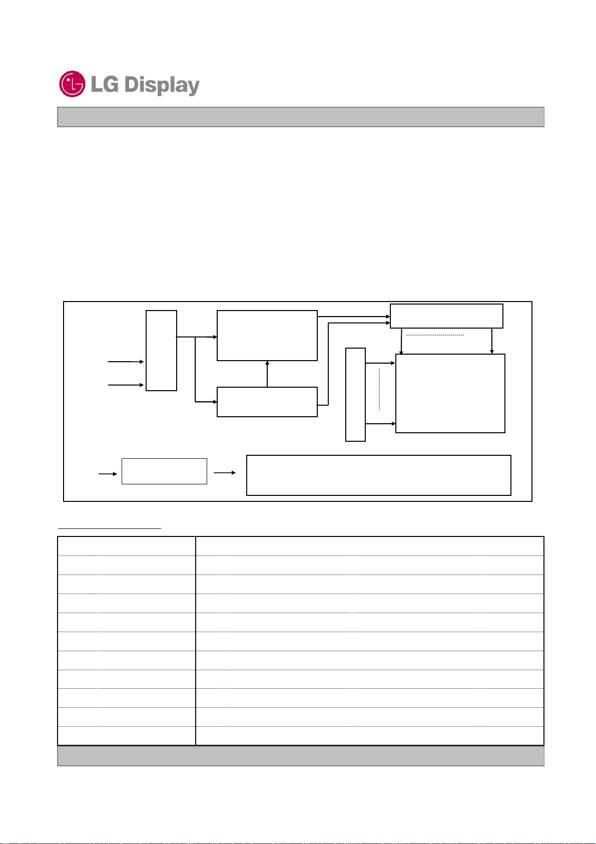
1. General Description
LM270WF1 is a Color Active Matrix Liquid Crystal Display with an integral Cold Cathode Fluorescent
Lamp(CCFL) backlight system without inverter. The matrix employs a-Si Thin Film Transistor as the active
element. It is a transmissive type display operating in the normally black mode. It has a 27 inch diagonally
measured active display area with Full HD resolution (1080 vertical by 1920 horizontal pixel array)
Each pixel is divided into Red, Green and Blue sub-pixels or dots which are arranged in vertical stripes.
Gray scale or the brightness of the sub-pixel color is de termined with a 8-bit gray scale signal for each dot,
thus, presenting a palette of more than 16,7M colors with Advanced-FRC (Frame Rate Control). . It has
been designed to apply the interface method that enables low power, high speed, low EMI. FPD Link or
compatible must be used as a LVDS (Low Voltage Dif ferential Signaling) chip. It is intended to support
applications where thin thickness, wide viewing angle, low power are critical factors and graphic displays are
important. It is intended to support displays where high brightness, super wide viewing angle,
high color saturation, and high color are important.
RGB, Dclk, DE
Hsync, Vsync
(LVDS 2 port)
(12.0V)
V
LCD
V
LAMP
CN1
(30pin)
2pin x 8CNs (High)
General Features
CN 2
Timing Control
Block
Power Circuit Block
Figure 1. Block diagram
27 inches(68.6cm) diagonalActive Screen Size
630(H) x 368.2(V) x 37.2(D) mm(Typ.) *Without InverterOutline Dimension
0.3114 mm x 0.3114 mmPixel Pitch
1920 horiz. By 1080 vert. Pixels RGB stripes arrangementPixel Format
Source Driver Circuit
Gate Driver circuit
G1
TFT-LCD Panel
(1920 × 1080 pixels)
G1080
Back light Assembly
(Direct Light Type_ U shape 7 CCFL)
S1920S1
8-bit with A-FRC, 16,777,216 colorsColor Depth
2
400 cd/m
(Center 1 point)Luminance, White
View Angle Free (R/L 170(Typ.), U/D 160(Typ.))Viewing Angle(CR>10)
Total 87.8 Watt (Typ.) ( 4.2 Watt
4220 g (typ.)Weight
Transmissive mode, normally WhiteDisplay Operating Mode
Surface Treatment
Hard coating(3H) & Anti-Glare treatment of the front polarizer
Ver 1.2 Feb, 04, 2009
@VLCD, 83.6 Watt @400cd/㎡])Power Consumption
4/ 32
Page 7
LM270WF1
Liquid Crystal Display
Product Specification
2. Absolute Maximum Ratings
The following are maximum values which, if exceeded, may cause faulty operation or damage to the unit.
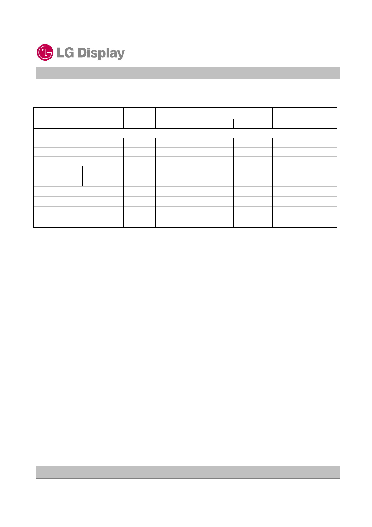
Table 1. ABSOLUTE MAXIMUM RATINGS
Parameter Notes
Power Input Voltage
Operating Temperature
Storage Temperature
Operating Ambient Humidity
Storage Humidity
Symbol
Values
MaxMin
500TOP
60-20TST
Units
Vdc12.4-0.3VLCD
°C
°C
%RH9010HOP
%RH9010HST
Note : 1. Temperature and relative humidity range are shown in the figure below.
Wet bulb temperature should be 39 °C Max, and no condensation of water.
90%
60
60%
Wet Bulb
Temperature [C]
30
20
10
0
50
40
40%
Humidity [(%)RH]
10%
at 25 ± 2°C
1
Storage
Operation
10 20 30 40 50 60 70 800-20
Dry Bulb Temperature [C]
Figure 2. Temperature and relative humidity
Ver 1.2 Feb, 04, 2009
5/ 32
Page 8
LM270WF1
Liquid Crystal Display
Product Specification
3. Electrical Specifications
3-1. Electrical Characteristics
It requires two power inputs. One is employed to power the LCD electronics and to drive the TFT array and
liquid crystal. The second input power for the CCFL, is typically generated by an inverter. The inverter is an
external unit to the LCDs.
Table 2-1. ELECTRICAL CHARACTERISTICS
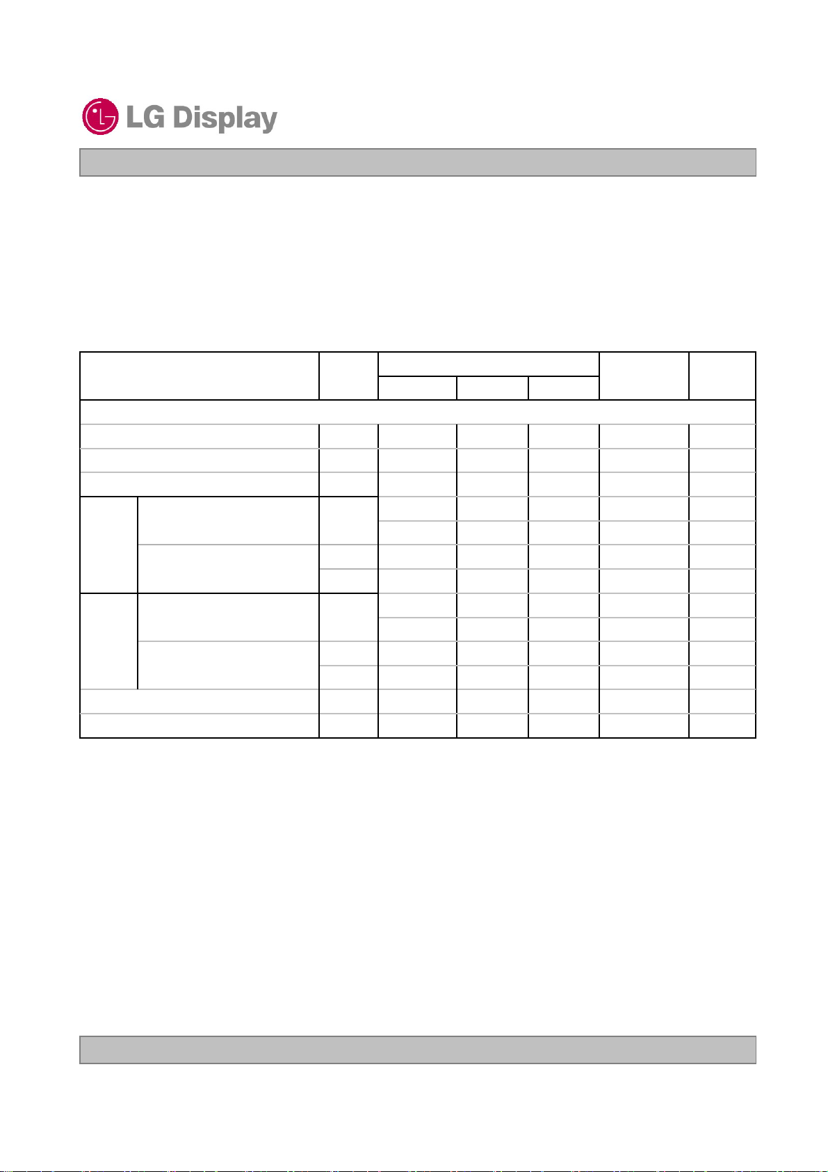
Parameter Symbol
MODULE :
Differential Impedance
Normal
status
Power Consumption
Power Supply Input Current
BDI
Status
Power Consumption
VLCDPower Supply Input Voltage
-
ILCDPower Supply Input Current
-
-Pc TYP
-Pc MAX
-
ILCD
-
Values
MaxTypMin
12.412.011.6
403350
565490
4.844.2
7.025.88
575500
590510
Vdc
Ohm11010090Zm
Note :
1. Permissive power ripple should be measured under VCC=12.0V, 25°C, fV(frame frequency)=MAX
condition and At that time, we recommend the bandwidth configuration of oscilloscope is to be under
20Mhz. See the next page.
NotesUnit
1mVp-p400VdRFPermissive Power Input Ripple
2mA
3mA
2Watt
3Watt
2mA
3mA
2Watt6.96.0-Pc TYP
3Watt7.086.12-Pc MAX
4A3.0--IRUSHRush current
2. The specified current and power consumption are under the V
=12.0V, 25 ± 2°C,fV=60Hz condition
LCD
whereas Mosaic and max power pattern shown in the [ Figure 3 ] is displayed.
3. The current is specified at the maximum current pattern.
4. Maximum Condition of Inrush current :
The duration of rush current is about 2ms and rising time of Input Voltage is 1ms(min.).
At any rising time of Input voltage, Keep the I2T Value by below Condition
Condition : I2T < 32*2ms
Ver 1.2 Feb, 04, 2009
6/ 32
Page 9
Liquid Crystal Display
Product Specification
• Permissive Power input ripple (VCC=5.0V, 25°C, fV(frame frequency)=MAX condition)
LM270WF1
White pattern
• Power consumption (VCC=5.0V, 25°C, fV (frame frequency=60Hz condition)
Typical power Pattern
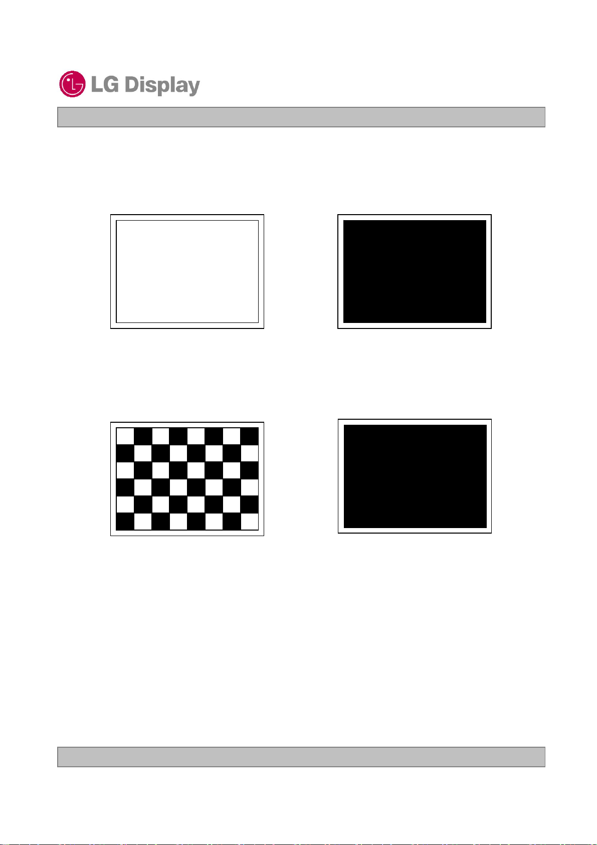
Figure 3. Mosaic pattern & Black Pattern for power consumption measurement
Black pattern
Max power Pattern
Ver 1.2 Feb, 04, 2009
7/ 32
Page 10
Product Specification
Table 2_2. ELECTRICAL CHARACTERISTICS
LM270WF1
Liquid Crystal Display
Parameter Symbol
LAMP :
at 25 °C
at 0 °C
Values
MaxTypMin
2250(3.0mA)1990(6.0mA)1900(7.0mA)VBLOperating Voltage
7.06.03.0IBLOperating Current
3000-3600--
RMS
RMS
V
RMS
V
RMS
Operating Frequency
Discharge Stabilization Time
Power Consumption
Life Time
Note : The design of the inverter must have specifications for the lamp in LCD Assembly.
The performance of the Lamp in LCM, for e xample life time or brightness, is e xtremely influenced by
the characteristics of the DC-AC inverter. So all the parameters of an inverter should be carefully
designed so as not to produce too much leakage current from high-voltage output of the inverter.
When you design or order the inverter, please make sure unwanted lighting caused by the mismatch
of the lamp and the inverter (no lighting, flicker, etc) ne ver occurs. When you confirm it, the LCD–
Assembly should be operated in the same condition as installed in you instrument.
※ Do not attach a conducting tape to lamp connecting wire.
If the lamp wire attach to a conducting tape, TFT-LCD Module has a low luminance and the inverter
has abnormal action. Because leakage current is occurred between lamp wire and conducting tape.
NotesUnit
1, 2V
1mA
1, 3VsEstablished Starting Voltage
4kHz80-40fBL
1, 5Min3.0Ts
6Watt93.183.647.3PBL
1, 7Hrs40,000
1. Specified values are for a single lamp.
2. Operating voltage is measured at 25 ± 2°C. The variance of the voltage is ± 10%.
3. The voltage above V
should be applied to the lamps for more than 1 second for start-up.
S
(Inverter open voltage must be more than lamp starting voltage.)
Otherwise, the lamps may not be turned on. The used lamp current is the lamp typical current.
4. Lamp frequency may produce interface with horizonta l synchronous frequency and as a result this may
cause beat on the display. Therefore lamp frequency shall be as away possible from the horizontal
synchronous frequency and from its harmonics in order to prevent interference.
5. Let’s define the brightness of the lamp after being lighted for 5 minutes as 100%.
T
is the time required for the brightness of the center of the lamp to be not less than 95%.
S
6. The lamp power consumption shown above does not include loss of external inverter.
The used lamp current is the lamp typical current. (P
= VBLx IBLx N
BL
Lamp
)
7. The life is determined as the time at which brightness of the lamp is 50% compared to that of initial
value at the typical lamp current on condition of continuous operating at 25 ± 2°C.
Ver 1.2 Feb, 04, 2009
8/ 32
Page 11
LM270WF1
Liquid Crystal Display
Product Specification
8. The output of the inverter must have symmetrical(negative and positive) voltage waveform and
symmetrical current waveform (Unsymmetrical ratio is less than 10%). Please do not use the inverter
which has unsymmetrical voltage and unsymmetrical current and spike wave.
Requirements for a system inverter design, which is intended to have a better display performance, a
better power efficiency and a more reliable lamp, are following.
It shall help increase the lamp lifetime and reduce leakage current.
a. The asymmetry rate of the inverter waveform should be less than 10%.
b. The distortion rate of the waveform should be within √2 ±10%.
* Inverter output waveform had better be more similar to ideal sine wave.
* Asymmetry rate:
I p
| I
p
–I –p| / I
rms
x 100%
I -p
* Distortion rate
I
(or I –p) / I
p
rms
9. The inverter which is combined with this LCM, is highly recommended to connect coupling(ballast)
condenser at the high voltage output side. When you use the inverter which has not coupling(ballast)
condenser, it may cause abnormal lamp lighting because of biased mercury as time goes.
10.In case of edgy type back light with over 4 parallel lamps, input current and voltage wave form should
be synchronized
Ver 1.2 Feb, 04, 2009
9/ 32
Page 12

LM270WF1
Liquid Crystal Display
Product Specification
3-2. Interface Connections
This LCD employs Two interface connections, a 30 pin connector is used for the module electronics and a
14Pin Connector is used for the integral backlight system.
3-2-1. LCD Module
- LCD Connector(CN1): KDF71G-30S-1H, (Manufactured by Hirose )
- Mating Connector : FI-X30C2L (Manufactured by JAE) or Equivalent
Table 3 MODULE CONNECTOR(CN1) PIN CONFIGURATION
1
2
3
4
5
6
7
8
9
10
11
12
13
14
15
SymbolNo
FR0M
FR0P
FR1M
FR1P
FR2M
FR2P
GND
FCLKINM
FCLKINP
FR3M
FR3P
SR0M
SR0P
GND
SR1M
Description
Minus signal of odd channel 0 (LVDS)
Plus signal of odd channel 0 (LVDS)
Minus signal of odd channel 1 (LVDS)
Plus signal of odd channel 1 (LVDS)
Minus signal of odd channel 2 (LVDS)
Plus signal of odd channel 2 (LVDS)
Ground
Minus signal of odd clock channel (LVDS)
Plus signal of odd clock channel (LVDS)
Minus signal of odd channel 3 (LVDS)
Plus signal of odd channel 3 (LVDS)
Minus signal of even channel 0 (LVDS)
Plus signal of even channel 0 (LVDS)
Ground
Minus signal of even channel 1 (LVDS)
No
16
17
18
19
20
21
22
23
24
25
26
27
28
29
30
Symbol
SR1P
GND
SR2M
SR2P
SCLKINM
SCLKINP
SR3M
SR3P
MPRT
NC
NC
DCR_OUT
ODC
VLCD
VLCD
Symbol
Plus signal of even channel 1 (LVDS)
Ground
Minus signal of even channel 2 (LVDS)
Plus signal of even channel 2 (LVDS)
Minus signal of even clock channel (LVDS)
Plus signal of even clock channel (LVDS)
Minus signal of even channel 3 (LVDS)
Plus signal of even channel 3 (LVDS)
BDI Control (GND: off, 3.3V:on)
Notes 4,5.6
No Connection
No Connection
Dynamic C/R output
ODC Control (GND: off, 3.3V:on)
Power Supply +12.0V
Power Supply +12.0V
Note: 1. All GND(ground) pins should be connected together and to Vss which should also be connected to
the LCD’s metal frame.
2. All V
LCD (power input) pins should be connected together.
3. Input Level of LVDS signal is based on the IEA 664 Standard.
4, MPRT and ODC control does not turn on at same time.
5. BL is 100% diming at MPRT on status..
6. On status of MPRT is support dynamic image.
Rear view of LCM
#1 #30
#1 #30
KDF71G-30S-1H
Ver 1.2 Feb, 04, 2009
[ Figure 4 ] Connector diagram
10 / 32
Page 13

Liquid Crystal Display
Product Specification
Table 4. REQUIRED SIGNAL ASSIGNMENT FOR Flat Link (TI:SN75LVDS83) Transmitter
Pin # Require SignalPin Name Pin # Require SignalPin Name
1 Power Supply for TTL InputVCC 29 Ground pin for TTLGND
2 TTL Input (R7)D5 30 TTL Input (DE)D26
3 TTL Input (R5)D6 31 TTL Level clock InputTXCLKIN
4 TTL Input (G0)D7 32 Power Down InputPWR DWN
5 Ground pin for TTLGND 33 Ground pin for PLLPLL GND
6 TTL Input (G1)D8 34 Power Supply for PLLPLL VCC
7 TTL Input (G2)D9 35 Ground pin for PLLPLL GND
8 TTL Input (G6)D10 36 Ground pin for LVDSLVDS GND
9 Power Supply for TTL InputVCC 37 Positive LVDS differential data output 3TxOUT3+
10 TTL Input (G7)D11 38 Negative LVDS differential data output 3TxOUT3-
LM270WF1
11 TTL Input (G3)D12 39 Positive LVDS differential clock outputTXCLKOUT+
12 TTL Input (G4)D13 40 Negative LVDS differential clock outputTXCLKOUT-
13 Ground pin for TTLGND 41 Positive LVDS differential data output 2TXOUT2+
14 TTL Input (G5)D14 42 Negative LVDS differential data output 2TXOUT2-
15 TTL Input (B0)D15 43 Ground pin for LVDSLVDS GND
16 TTL Input (B6)D16 44 Power Supply for LVDSLVDS VCC
17 Power Supply for TTL InputVCC 45 Positive LVDS differential data output 1TXOUT1+
46 Negative LVDS differential data output 1TXOUT1-18 TTL Input (B7)D17
19 TTL Input (B1)D18
20 TTL Input (B2)D19
22 TTL Input (B3)D20
23 TTL Input (B4)D21
24 TTL Input (B5)D22
25 TTL Input (RSVD)D23
26 Power Supply for TTL InputVCC 54 TTL Input (R2)D2
47 Positive LVDS differential data output 0TXOUT0+
48 Negative LVDS differential data output 0TXOUT0-
49 Ground pin for LVDSLVDS GND21 Ground pin for TTL InputGND
50 TTL Input (R6)D27
51 TTL Input (R0)D0
52 TTL Input (R1)D1
53 Ground pin for TTLGND
55 TTL Input (R3)D327 TTL Input (HSYNC)D24
56 TTL Input (R4)D428 TTL Input (VSYNC)D25
Notes : Refer to LVDS Transmitter Data Sheet for detail descriptions.
Ver 1.2 Feb, 04, 2009
11 / 32
Page 14

LVDS Input characteristics
1. DC Specification
LM270WF1
Liquid Crystal Display
Product Specification
LVDS Common mode Voltage
LVDS Input Voltage Range
2. AC Specification
LVDS Clock to Data Skew Margin
LVDS Clock to Clock Skew Margin (Even to Odd)
Maximum deviation
of input clock frequency during SSC
|LVDS Differential Voltage
ID
CM
IN
SKEW
SKEW
SKEW
SKEW_EO
DEV
- 600
-1/7
NotesUnitMaxMinSymbolDescription
-mV600100|V
-V1.80.6V
-V2.10.3V
NotesUnitMaxMinSymbolDescription
90MHz > Fclk ≥ 85MHzPs+ 350-350t
85MHz > Fclk ≥ 65MHzps+ 400-400t
65MHz > Fclk ≥ 25MHz
ps+ 600t
+ 1/7t
T
clk
%± 3-F
-
-
Maximum modulation frequency
of input clock during SSC
MOD
Ver 1.2 Feb, 04, 2009
KHz200-F
-
12 / 32
Page 15

Freq.
F
max
F
center
F
min
Product Specification
< Clock skew margin between channel >
LM270WF1
Liquid Crystal Display
* F
F
center
DEV
3. Data Format
1) LVDS 2 Port
1
F
MOD
< Spread Spectrum >
Time
< LVDS Data Format >
Ver 1.2 Feb, 04, 2009
13 / 32
Page 16
2) LVDS 1 Port
RCLK+
LM270WF1
Liquid Crystal Display
Product Specification
RA+/-
RB+/-
RC+/-
RD+/-
R3 R2
G4 G3
B5 B4
G7 G6
Previous (N-1 )th Cycle Next(N+1)th Cycle
R1 R0
G2 G1
B3 B2
R7 R6
G0 R5 R4 R3 R2 R1 R0
B1 B0 G5 G4 G3 G2 G1
DE VSYNC HSYNC B5 B4 B3 B2
X B7 B6 G7 G6 R7 R6
Current (Nth ) Cycle
G0
B1
DE
VSYNC HSYNC
X
R5 R4
B0 G5
B7 B6
Ver 1.2 Feb, 04, 2009
14 / 32
Page 17

LM270WF1
Liquid Crystal Display
Product Specification
Table 5. BACKLIGHT CONNECTOR PIN CONFIGURATION(CN1,CN2, CN3, CN 4,CN5 ,CN6, CN7)
The backlight lamp connector is a model 1006-12102 (CN1/CN2/CN3/CN4/CN5/CN6/CN7) manufactured by C-NET.
The mating connector part number are 1006-66202 (manufactured by C-NET) or equivalent. The pin configuration for
the connector is shown in the table below.
Pin
1,2
Symbol
HV
Description
High Voltage for Lamp
Note : 1. The high voltage power terminal is colored Red/White
<BACKLIGHT CONNECTOR DIAGRAM>
NOTES
1
U-LAMP
CN1 CN2
CN3
Ver 1.2 Feb, 04, 2009
CN4
CN5
CN6
CN7
15 / 32
Page 18

LM270WF1
Liquid Crystal Display
Product Specification
3-3. Signal Timing Specifications
This is signal timing required at the input of the TMDS transmitter. All of the interface signal timing should be
satisfied with the following specifications for it’s proper operation.
Table 5. TIMING TABLE
NoteUnitMaxTypMinSymbolITEM
DCLK
Hsync
Vsync
tCLKPeriod
-Frequency
tHPPeriod
tHVHorizontal Valid
tHBHorizontal Blank
fHFrequency
tWHWidth
tHBPHorizontal Back Porch
tHFPHorizontal Front Porch
tVPPeriod
tVVVertical Valid
tVBVertical Blank
fVFrequency
tWVWidth
16012858
886664
644820
484820
ns15.3813.8911.76
MHz907265
tCLK112010881018
tCLK960960960
KHz
tCLK483218
tHP125011001087
tHP108010801080
tHP170207
Hz756050
tHP4241
tVBPVertical Back Porch
tVFPVertical Front Porch
Note: Hsync period and Hsync width-active should be even number times of t
times of t
CLK, display control signal can be asynchronous. In order to operate this LCM a Hsync,
6485
6481
CLK. If the value is odd number
Vsyn, and DE(data enable) signals should be used.
1. The performance of the electro-optical characteristics may be influenced by variance of the vertical
refresh rates.
2. Vsync and Hsync should be keep the above specification.
3. Hsync Period, Hsync Width, and Horizontal Back Porch should be any times of of character
number(8).
4. The polarity of Hsync, Vsync is not restricted.
5. BDI on status : Vsync opearte at 60hz
Ver 1.2 Feb, 04, 2009
16 / 32
Page 19

3-4. Signal Timing Waveforms
LM270WF1
Liquid Crystal Display
Product Specification
Hsync, Vsync, DE, DATA
t
CLK
Dclk
INVALID
DATA
DE(Data Enable)
Hsync
t
WH
0.5VDD
0.7VDD
0.3VDD
VALID
Data are latched at the falling edge of DCLK
t
HP
INVALID
t
HBP
t
HV
DE(Data Enable)
t
VP
t
WV
Vsync
t
VBP
t
VV
DE(Data Enable)
Ver 1.2 Feb, 04, 2009
t
t
HFP
VFP
17 / 32
Page 20
LM270WF1
Liquid Crystal Display
Product Specification
3-5. Color Data Reference
The Brightness of each primary color(red,green,blue) is based on the 8-bit gray scale data input for the color;
the higher the binary input, the brighter the color. The table below provides a reference for color versus data
input.
Table 6. COLOR DATA REFERENCE
Input Color Data
Basic
Color
RED
Color
Black 0 0 0 0 0 0 0 00 0 0 0 0 0 0 00 0 0 0 0 0 0 0
Red (255)
Green (255)
Blue (255)
Cyan
Magenta
Yellow
White
MSB LSB
RED
GREEN
MSB LSB
BLUE
MSB LSB
B7 B6 B5 B4 B3 B2 B1 B0G7 G6 G5 G4 G3 G2 G1 G0R7 R6 R5 R4 R3 R2 R1 R0
0 0 0 0 0 0 0 00 0 0 0 0 0 0 01 1 1 1 1 1 1 1
0 0 0 0 0 0 0 01 1 1 1 1 1 1 10 0 0 0 0 0 0 0
1 1 1 1 1 1 1 10 0 0 0 0 0 0 00 0 0 0 0 0 0 0
1 1 1 1 1 1 1 11 1 1 1 1 1 1 10 0 0 0 0 0 0 0
1 1 1 1 1 1 1 10 0 0 0 0 0 0 01 1 1 1 1 1 1 1
0 0 0 0 0 0 0 01 1 1 1 1 1 1 11 1 1 1 1 1 1 1
1 1 1 1 1 1 1 11 1 1 1 1 1 1 11 1 1 1 1 1 1 1
0 0 0 0 0 0 0 00 0 0 0 0 0 0 00 0 0 0 0 0 0 0RED (000) Dark
0 0 0 0 0 0 0 00 0 0 0 0 0 0 00 0 0 0 0 0 0 1RED (001)
............
0 0 0 0 0 0 0 00 0 0 0 0 0 0 01 1 1 1 1 1 1 0RED (254)
0 0 0 0 0 0 0 00 0 0 0 0 0 0 01 1 1 1 1 1 1 1RED (255)
0 0 0 0 0 0 0 00 0 0 0 0 0 0 00 0 0 0 0 0 0 0GREEN (000) Dark
GREEN
BLUE (000) Dark
BLUE
Ver 1.2 Feb, 04, 2009
0 0 0 0 0 0 0 00 0 0 0 0 0 0 10 0 0 0 0 0 0 0GREEN (001)
............
0 0 0 0 0 0 0 01 1 1 1 1 1 1 00 0 0 0 0 0 0 0GREEN (254)
0 0 0 0 0 0 0 01 1 1 1 1 1 1 10 0 0 0 0 0 0 0GREEN (255)
0 0 0 0 0 0 0 00 0 0 0 0 0 0 00 0 0 0 0 0 0 0
0 0 0 0 0 0 0 10 0 0 0 0 0 0 00 0 0 0 0 0 0 0BLUE (001)
............
1 1 1 1 1 1 1 00 0 0 0 0 0 0 00 0 0 0 0 0 0 0BLUE (254)
1 1 1 1 1 1 1 10 0 0 0 0 0 0 00 0 0 0 0 0 0 0BLUE (255)
18 / 32
Page 21

3-6. Power Sequence
LM270WF1
Liquid Crystal Display
Product Specification
90% 90%
Power supply for LCD
Vcc
0V
Interface signal
V
I
Option siganl
(ODC)
Power for LAMP
Table 7. POWER SEQUENCE
Parameter
10%
T1
T2 T5 T7
Valid data
T8
T3
T9
T4
Lamp on
OFF
Values
10%
OFF
Units
MaxTypMin
ms10-0.5T1
Notes : 1. Please avoid floating state of interface signal at invalid period.
2. When the interface signal is invalid, be sure to pull down the power supply for LCD V
3. Lamp power must be turn on after power supply for LCD and interface signal are valid.
Ver 1.2 Feb, 04, 2009
ms50-0.01T2
ms--500T3
--200T4
ms
ms50-0.01T5
ms-300T7
ms0 < T8 < T2T8
ms0 < T9 < T5T9
LCD
to 0V.
19 / 32
Page 22

LM270WF1
Liquid Crystal Display
Product Specification
4. Optical Specifications
Optical characteristics are determined after the unit has been ‘ON’ for approximately 30 minutes
in a dark environment at 25±2°C. The values specified are at an approximate distance 50cm from the LCD
surface at a viewing angle of Φ and θ equal to 0 ° and aperture 1 degree.
FIG. 1 presents additional information concerning the measurement equipment and method.
Optical Stage(x,y)
LCD Module
FIG. 6 Optical Characteristic Measurement Equipment and Method
Table 9. OPTICAL CHARACTERISTICS
SymbolParameter
Surface Luminance, white
Luminance Variation
Response Time
Color Coordinates
[CIE1931]
Viewing Angle (CR>5)
x axis, right(φ=0°)
x axis, left (φ=180°)
y axis, up (φ=90°)
y axis, down (φ=270°)
Viewing Angle (CR>10)
x axis, right(φ=0°)
x axis, left (φ=180°)
y axis, up (φ=90°)
y axis, down (φ=270°)
Rise Time
Decay Time
Gray to Gray
MPRT
RED
GREEN
BLUE
WHITE
δ
WHITE
MPRT
Rx
θr
θl
θu
θd
θr
θl
θu
θd
WH
GTG
Pritchard 880 or
equivalent
50cm
(Ta=25 °C, V
R
D
Typ
-0.03
=12.0V, fV=60Hz Dclk=144MHz, IBL=6mA)
LCD
Values
MaxTypMin
1000700CRContrast Ratio
400320L
0.661
0.318Ry
0.207Gx
0.668Gy
0.144Bx
0.068By
0.313Wx
0.329Wy
8875
8570
8570
8570
7560
8570
Typ
+0.03
2
Degree8875
NotesUnits
1
2cd/m
3%75
4ms41-Tr
4ms84-Tr
5ms62T
6ms1510T
7
7Degree8570
82.2Gray Scale
Ver 1.2 Feb, 04, 2009
20 / 32
Page 23

Product Specification
…
Notes 1. Contrast Ratio(CR) is defined mathematically as :
LM270WF1
Liquid Crystal Display
Contrast Ratio =
2. Surface luminance is luminance value at No.1 point across the LCD surface 50cm
from the surface with all pixels displaying white. For more information see FIG 6.
3. The variation in surface luminance , δ WHITE is defined as :
δ
WHITE
Measuring point for surface luminance & measuring point for luminance variation
B
Surface Luminance with all white pixels
Surface Luminance with all black pixels
)L .. ,L,Minimum(L
on9on2on1
=
H
A
23
×
)L .... ,L ,(L Maximum
on9on2on1
(%)100
4
H/10
V
V/10
A : H/4 mm
B : V/4 mm
@ H,V : Active Area
Ver 1.2 Feb, 04, 2009
5
78
[ FIGURE 7 ] Measure Point for Luminan ce
1
6
9
Active Ar e a
21 / 32
Page 24

Liquid Crystal Display
Product Specification
4. The response time is defined as the following figure and shall be measured by switching
the input signal for “black” and “white”.
Response time is the time required for the display to transition from white to black (Rise Time,
T
rR) and from black to white (Decay Time, TrD).
LM270WF1
%
Tr
R
Tr
D
100
90
Optical
white black white
response
10
0
[ FIGURE 8] Response Time
5, The gray to gray response time is defined as the following figure and shall be measured by switching
the input signal for “Gray To Gray”.
- Gray step : 5 step
-T
GTG_AVR is the total average time at rising time and falling time for “Gray To Gray”.
-T
GTG_MAX is the max time at rising time or falling time for “Gray To Gray”.
Table 10. Gray to gray response time table
Gray to Gray
G255
G191
Falling Time
G127
G63
G0
Ver 1.2 Feb, 04, 2009
Rising Time
G0G63G127G191G255
22 / 32
Page 25

LM270WF1
Liquid Crystal Display
Product Specification
6. MPRT is defined as the 10% to 90% blur-edge width Bij(pixels) and scroll speed U(pixels/frame)
at the moving picture.
MPRT is defined as 10% to 90% blur-edge with Bij(pixels) and scroll speed U(pixels/frame)at the moving
picture.
1
M =
Bij (i=j)
U
Example) Bij = 12pixels, U = 10pixels / 120Hz
M = 12pixels / (10pixels / 120Hz)
= 12pixels / {10pixels / (1/120)s}
= 12 / 1,200 s
= 10 ms
[ FIGURE 9] MPRT
L
L
j
90%
10%
i
B
ij
Ver 1.2 Feb, 04, 2009
23 / 32
Page 26

LM270WF1
Liquid Crystal Display
Product Specification
7. Viewing angle is the angle at which the contrast ratio is greater than 10 or 5. The angles are
determined for the horizontal or x axis and the vertical or y axis with respect to the z axis
which is normal to the LCD surface. For more information see FIG. 9 .
<Dimension of viewing angle range>
φ
= 180°, Left
φ
= 270°, Down
8, Gray scale specification
Gamma Value is approximately 2.2. For more information see Table 11
Table 11. Gray Scale Specification
Normal
E
Y
φ
= 90°, Up
θ
φ
φ
= 0°, Right
[ FIGURE 10 ] Viewing angle
Relative Luminance [%] (Typ.)Gray Level
31
63
95
127
159
191
223
255
Ver 1.2 Feb, 04, 2009
0.10
1.2
4.7
11.7
21.2
35.2
53.0
75.4
100
24 / 32
Page 27

LM270WF1
Liquid Crystal Display
Product Specification
5. Mechanical Characteristics
The contents provide general mechanical characteristics. In addition the figures in the next page are detailed
mechanical drawing of the LCD.
630mmHorizontal
Outline Dimension
Bezel Area
Active Display Area
Typ : 4220 g , Max : 4430 gWeight
Surface Treatment
Hard coating(3H)
Anti-glare treatment of the front polarizer
Notes : Please refer to a mechanic drawing in terms of tolerance at the next page.
368.2mmVertical
37.2mmDepth
602mmHorizontal
340.4mmVertical
597.89mmHorizontal
336.31mmVertical
Ver 1.2 Feb, 04, 2009
25 / 32
Page 28

<FRONT VIEW>
LM270WF1
Liquid Crystal Display
Product Specification
Ver 1.2 Feb, 04, 2009
26 / 32
Page 29

<REAR VIEW>
LM270WF1
Liquid Crystal Display
Product Specification
Ver 1.2 Feb, 04, 2009
27 / 32
Page 30

6. Reliability
Environment test condition
5
Vibration test
(non-operating)
LM270WF1
Liquid Crystal Display
Product Specification
ConditionTest ItemNo
Ta= 60°C 240hHigh temperature storage test1
Ta= -20°C 240hLow temperature storage test2
Ta= 50°C 50%RH 240hHigh temperature operation test3
Ta= 0°C 240hLow temperature operation test4
Wave form : random
Vibration level : 1.0Grms
Bandwidth : 10-300Hz
Duration : X,Y,Z, 10min
One time each direction
Shock level : 100G
6
8
9
Shock test
(non-operating)
Humidity condition Operation7
Altitude
storage / shipment
Maximum Storage Humidity for
4 corner light leakage Mura.
Waveform : half sine wave, 2ms
Direction : ±X, ±Y, ±Z
One time each direction
Ta=
40 °C ,90%RH
0 - 40,000 feet(12192m)
Max 70%RH , Ta=40℃
Ver 1.2 Feb, 04, 2009
28 / 32
Page 31

LM270WF1
Liquid Crystal Display
Product Specification
7. International Standards
7-1. Safety
a) UL 60950-1:2003, First Edition, Underwriters Laboratories, Inc.,
Standard for Safety of Information Technology Equipment.
b) CAN/CSA C22.2, No. 60950-1-03 1
Standard for Safety of Information Technology Equipment.
c) EN 60950-1:2001, First Edition,
European Committee for Electro technical Standardization(CENELEC)
European Standard for Safety of Information Technology Equipment.
st
Ed. April 1, 2003, Canadian Standards Association,
7-2. EMC
a) ANSI C63.4 “Methods of Measurement of Radio-Noise Emissions from Low-Voltage Electrical and
Electrical Equipment in the Range of 9kHZ to 40GHz. “American National Standards Institute(ANSI),
1992
b) C.I.S.P.R. “Limits and Methods of Measurement of Radio Interface Characteristics of Information
Technology Equipment.“ International Special Committee on Radio Interference.
c) EN 55022 “Limits and Methods of Measurement of Radio Interface Characteristics of Information
Technology Equipment.“ European Committee for Electro technical Standardization.(CENELEC), 1998
( Including A1: 2000 )
Ver 1.2 Feb, 04, 2009
29 / 32
Page 32

Product Specification
8. Packing
8-1. Designation of Lot Mark
a) Lot Mark
ABCDEFGHIJKLM
A,B,C : SIZE(INCH) D : YEAR
E : MONTH F ~ M : SERIAL NO.
Note
1. YEAR
LM270WF1
Liquid Crystal Display
Year
Mark
321
200452005
4
200320022001
2006720078200892009
6
2. MONTH
Month
Mark
Apr5May
4
Jun
6
Jul8Aug9Sep
7
b) Location of Lot Mark
Serial No. is printed on the label. The label is attached to the backside of the LCD module.
This is subject to change without prior notice.
8-2. Packing Form
a) Package quantity in one box : 5EA
b) Box Size : 747X335X466
2010
0
Oct
A
Nov
B
DecMarFebJan
C321
Ver 1.2 Feb, 04, 2009
30 / 32
Page 33

LM270WF1
Liquid Crystal Display
Product Specification
9. PRECAUTIONS
Please pay attention to the followings when you use this TFT LCD module.
9-1. MOUNTING PRECAUTIONS
(1) You must mount a module using holes arranged in four corners or four sides.
(2) You should consider the mounting structure so that uneven force (ex. Twisted stress) is not applied to the
module. And the case on which a module is mounted should have sufficient strength so that external
force is not transmitted directly to the module.
(3) Please attach the surface transparent protective plate to the surface in order to protect the polarizer.
Transparent protective plate should have sufficient strength in order to the resist external force.
(4) You should adopt radiation structure to satisfy the temperature specification.
(5) Acetic acid type and chlorine type materials for the cover case are not desirable because the former
generates corrosive gas of attacking the polarizer at high temperature and the latter causes circuit break
by electro-chemical reaction.
(6) Do not touch, push or rub the exposed polarizers with glass, tweezers or anything harder than HB
pencil lead. And please do not rub with dust clothes with chemical treatment.
Do not touch the surface of polarizer for bare hand or greasy cloth.(Some cosmetics are detrimental
to the polarizer.)
(7) When the surface becomes dusty, please wipe gently with absorbent cotton or other soft materials like
chamois soaks with petroleum benzene. Normal-hex ane is recommended for cleaning the adhesives
used to attach front / rear polarizers. Do not use acetone, toluene and alcohol because they cause
chemical damage to the polarizer.
(8) Wipe off saliva or water drops as soon as possible. Their long time contact with polarizer causes
deformations and color fading.
(9) Do not open the case because inside circuits do not have sufficient strength.
9-2. OPERATING PRECAUTIONS
(1) The spike noise causes the mis-operation of circuits. It should be lower than following voltage :
V=±200mV(Over and under shoot voltage)
(2) Response time depends on the temperature.(In lower temperature, it becomes longer.)
(3) Brightness depends on the temperature. (In lower temperature, it becomes lower.)
And in lower temperature, response time(required time that brightness is stable after turned on) becomes
longer.
(4) Be careful for condensation at sudden temperature change. Condensation makes damage to polarizer or
electrical contacted parts. And after fading condensation, smear or spot will occur.
(5) When fixed patterns are displayed for a long time, remnant image is likely to occur.
(6) Module has high frequency circuits. Sufficient suppression to the electromagnetic interference shall be
done by system manufacturers. Grounding and shielding methods may be important to minimized the
interference.
(7) Please do not give any mechanical and/or acoustical impact to LCM. Otherwise, LCM can’t be operated
its full characteristics perfectly.
(8) A screw which is fastened up the steels should be a machine screw.
(if not, it causes metallic foreign material and deal LCM a fatal blow)
(9) Please do not set LCD on its edge.
Ver 1.2 Feb, 04, 2009
31 / 32
Page 34

LM270WF1
Liquid Crystal Display
Product Specification
9-3. ELECTROSTATIC DISCHARGE CONTROL
Since a module is composed of electronic circuits, it is not strong to electrostatic discharge. Make certain that
treatment persons are connected to ground through wrist band etc. And don’t touch interface pin directly.
9-4. PRECAUTIONS FOR STRONG LIGHT EXPOSURE
Strong light exposure causes degradation of polarizer and color filter.
9-5. STORAGE
When storing modules as spares for a long time, the following precautions are necessary.
(1) Store them in a dark place. Do not expose the module to sunlight or fluorescent light. Keep the temperature
between 5°C and 35°C at normal humidity.
(2) The polarizer surface should not come in contact with any other object.
It is recommended that they be stored in the container in which they were shipped.
9-6. HANDLING PRECAUTIONS FOR PROTECTION FILM
(1) The protection film is attached to the bezel with a small masking tape.
When the protection film is peeled off, static electricity is generated between the film and polarizer.
This should be peeled off slowly and carefully by people who are electrically grounded and with well ionblown equipment or in such a condition, etc.
(2) When the module with protection film attached is stored for a long time, sometimes there remains a very
small amount of glue still on the bezel after the protection film is peeled of f.
(3) You can remove the glue easily. When the glue remains on the bezel surface or its vestige is recognized,
please wipe them off with absorbent cotton waste or other soft material like chamois soaked with normalhexane.
Ver 1.2 Feb, 04, 2009
32 / 32
 Loading...