

Page 1
* The date(Create Date, Approved Date, Check Date) is based on Korean standard time(GMT+9)
Created Date 2011-08-20 09:22 (Korea Time)
Requested by
Subject [Approval Formal] EAJ61990301/EAJ61990302(LGD 23"W IPS 3D FPR_LM230WFA-SLA2/3)
EDMS Attributes
Component Development Information
Component Development Information
Component Development InformationComponent Development Information
Model : D237IPS-PNY
Approval type : New (●) Limit () Revision () 4M ()
HSMS (RoHS) : Complete (●) Limit Approval () Warranty Approval ()
Reliability test : Needless ( ) Need (Test Report No: ● )
Class Name : LCD,Module-TFT
Part Number : EAJ61990301/EAJ61990302
Maker : LG Display
Specification : LM230WFA-SLA2 FHD 23.0INCH 1920X1080 250CD COLOR 72% 16/9 1000:1,R/T 14ms(GTG),V/A 178/178,ZBD
Key part list : P8,GZ,C/F LGD,Pol LGC,S-IC OKI,GIP,T-con LGD,B/L ass'y GZ Heesung
WLED WRL(7020), DBEF+Prism+Diffuser
Development History : 23"W IPS 3D FPR New module development
최찬용 ( Monitor양산그룹 / 주임연구원 , 82-031-610-6597 )
Retention 5 Year
Security Grade Internal use (Only)
승인원 회람 양식
Tag
★Safety Standard Parts [안전규격부품 List]
Power Cord, Power Plug, X / Y-Capacitor, Power Switch, Fuse, SMPS Trans, Stand-By Trans, Photo coupler,
Insulation (절연) Resistor, Discharge (방전)Resistor, Fusing Resistor, FBT,CPT, CPT Socket, DY, D-Coil,
Line Filter, PCB Material, Front / Back-cover Material, Relay(1-2차간), Varistor, Adaptor, PSU(Power supply unit)
★EMC Standard Parts [전파규격 부품 List]
Power Plug, Line Filter, X-Capacitor, Y-Capacitor, SMPS Trans, Tuner, Saw-Filter, Shield Case, Oscillator, Pattern Change
★Green [유해물질 확인사항]
This item must meet the standards of LG Electronics for six major substances as designated by RoHS for control.
Approval Type Status Approved Date Approved by / Comment
손경조 ( HE규격1그룹 / 선임연구원 )
Comment : 확인합니다.
차상호 ( HE규격1그룹 / 책임연구원 )
Comment : 확인합니다.
윤성욱 ( HE규격1그룹 / 책임연구원 )
Comment : 확인합니다.
이종호 ( Monitor회로개발그룹 / 주임연구원 )
Comment : 확인합니다.
김종태 ( Monitor회로개발그룹 / 수석연구원 )
김병근 ( Slim LED TDR / 주임연구원 )
Comment : 확인합니다.
윤석재 ( Monitor양산그룹 / 책임연구원 )
Comment : IIS에 3D관련 항목 update하여 release바랍니다.
배권일 ( Monitor양산그룹 / 수석연구원 )
Comment : 확인합니다
Approval Line
Agree Approved 2011-08-20 12:00
Agree Approved 2011-08-22 07:58
Agree Approved 2011-08-22 10:10
Agree Approved 2011-08-22 13:48
Agree Approved 2011-08-23 09:53
Agree Approved 2011-08-24 07:58
Approval Approved 2011-08-24 09:04
Approval Approved 2011-08-24 10:31
정길식 ( Slim LED TDR / 책임연구원 )
윤시열 ( Monitor R&D기획그룹 / 수석연구원 )
송재학 ( Monitor양산품질보증그룹 / 차장 )
김상인 ( Monitor양산그룹 / 주임연구원 )
한상석 ( LGEND MNT R&D.Development Group / 책임연구원 )
장기영 ( IPS TDR / 책임연구원 )
이기형 ( Slim LED TDR / 선임연구원 )
최찬용 ( Monitor양산그룹 / 주임연구원 )
송성호 ( 3D Monitor TDR / 선임연구원 )
김경진 ( LCD TV부품품질보증계 / 기사 )
김철회 ( LGEND MNT R&D.Mechanic Group / 선임연구원 )
허희준 ( IPS TDR / 선임연구원 )
김현석 ( Monitor혁신추진그룹 / 선임연구원 )
이경원 ( Monitor양산그룹 / 주임연구원 )
이종호 ( Monitor회로개발그룹 / 주임연구원 )
Page 2
CC
EDMS Doc Link
Attached Local Files
김부영 ( 3D Monitor TDR / 주임연구원 )
류정일 ( Monitor양산그룹 / 주임연구원 )
김영주 ( Monitor R&D기획그룹 / 연구원 )
조대현 ( Monitor양산그룹 / 주임연구원 )
류주혁 ( IPS TDR / 연구원 )
정회화 ( Monitor개발품질보증그룹 / 과장 )
박진수 ( Monitor개발품질보증그룹 / 과장 )
임창성 ( Monitor양산품질보증그룹 / 과장 )
김아련 ( Monitor R&D기획그룹 / 주임연구원 )
윤석재 ( Monitor양산그룹 / 책임연구원 )
박영춘 ( Monitor양산그룹 / 주임연구원 )
강지훈 ( Monitor R&D기획그룹 / 연구원 )
박남규 ( Monitor회로개발그룹 / 연구원 )
이종수 ( Monitor양산그룹 / 주임연구원 )
엄정훈 ( 3D Monitor TDR / 선임연구원 )
박경열 ( Monitor양산그룹 / 선임연구원 )
송종인 ( Monitor R&D기획그룹 / 연구원 )
김경난 ( Monitor개발품질보증그룹 / 사원 )
황동선 ( LGEND MNT R&D.S/W Group / 수석연구원 )
김종태 ( Monitor회로개발그룹 / 수석연구원 )
홍의성 ( LGEND MNT R&D.VP / 수석연구원 )
배권일 ( Monitor양산그룹 / 수석연구원 )
이문희 ( LGEND MNT R&D.Mechanic Group / 책임연구원 )
한태수 ( LCD TV부품품질보증계 / 기장 )
박철진 ( LCD TV부품품질보증계 / 기정 )
hui kang ( LGEND MNT R&D.Module Development Part / manager b )
xiangtai jin ( LGEND MNT R&D.Module Development Part / officer 1 )
xing jin ( LGEND MNT R&D.Module Development Part / )
[LGE Approval] CAS_LM230WFA-SLA2(ZBD).pdf
[LGE Approval] CAS_LM230WFA-SLA3(Non-ZBD).pdf
[LGE Approval] IIS_LM230WFA-SLA2(ZBD).pdf
[LGE Approval] IIS_LM230WFA-SLA3(Non-ZBD).pdf
LM230WFA-SLA2 TCO document.pdf
LM230WFA-SLA2 Key part&module comparison sheet.zip
LM230WFA-SLA2 Safety document.zip
LM230WFA-SLA2 LGD Test Report.zip
LM230WFA-SLA2_3D Drawing.zip
Page 3
( ) Preliminary Specification
SUFFIX
SLA2
(
●●●●
) Final Specification
LM230WFA
Liquid Crystal Display
Product Specification
SPECIFICATION
FOR
APPROVAL
23” Full HD TFT LCDTitle
BUYER
MODEL
APPROVED BY
/
/
/
LGE
SIGNATURE
DATE
SUPPLIER LG Display Co., Ltd.
*MODEL LM230WFA
*When you obtain standard approval,
please use the above model name without suffix
APPROVED BY
K.G Park / G.Manager
REVIEWED BY
H.Y Kim / Manager
PREPARED BY
S.W Yoo / Engineer
SIGNATURE
DATE
Please return 1 copy for your confirmation with
your signature and comments.
Ver. 1.0 Aug. 10 . 2011
MNT Products Engineering Dept.
LG Display Co., Ltd
1 / 34
Page 4
Product Specification
16
16
Contents
LM230WFA
Liquid Crystal Display
No ITEM
COVER
CONTENTS
RECORD OF REVISIONS
1 GENERAL DESCRIPTION
2 ABSOLUTE MAXIMUM RATINGS
3 ELECTRICAL SPECIFICATIONS
3-1 ELECTRICAL CHARACTREISTICS
3-2 INTERFACE CONNECTIONS
3-3 SIGNAL TIMING SPECIFICATIONS
3-4 SIGNAL TIMING WAVEFORMS
3-5 COLOR INPUT DATA REFERNECE
3-6 POWER SEQUENCE
3-7 V
4 OPTICAL SPECIFICATIONS
Power Dip Condition
LCD
Page
1
2
3
4
5
6
6
9
14
15
17
18
19
4-1 2D Optical specifications
4-2 3D Optical Specification
5 MECHANICAL CHARACTERISTICS
6 RELIABLITY
7 INTERNATIONAL STANDARDS
7-1 SAFETY
7-2 EMC
7-3 ENVIRONMENT
8 PACKING
8-1 DESIGNATION OF LOT MARK
8-2 PACKING FORM
9 PRECAUTIONS 35, 36
19
25
29
32
33
33
33
33
34
34
34
Ver. 1.0 Aug. 10 . 2011
2 / 34
Page 5
Product Specification
RECORD OF REVISIONS
LM230WFA
Liquid Crystal Display
Revision
No
0.1 Mar. 10, 2011 - First Draft, Preliminary Specifications
0.2 Jun. 09, 2011 4 Update General Features
1.0 Aug. 10, 2011 Final specification
Revision
Date
Page Description
13 Update Fig. 5 Backlight connector view
19 Update Color Coordinates
26 Update 3D Optical Specification
29 Update 5. Mechanical Characteristics
30 Update Front View
31 Update Rear View
25 Insert 3D C/T Max. 3%
Ver. 1.0 Aug. 10 . 2011
3 / 34
Page 6
LM230WFA
G1080
Liquid Crystal Display
Product Specification
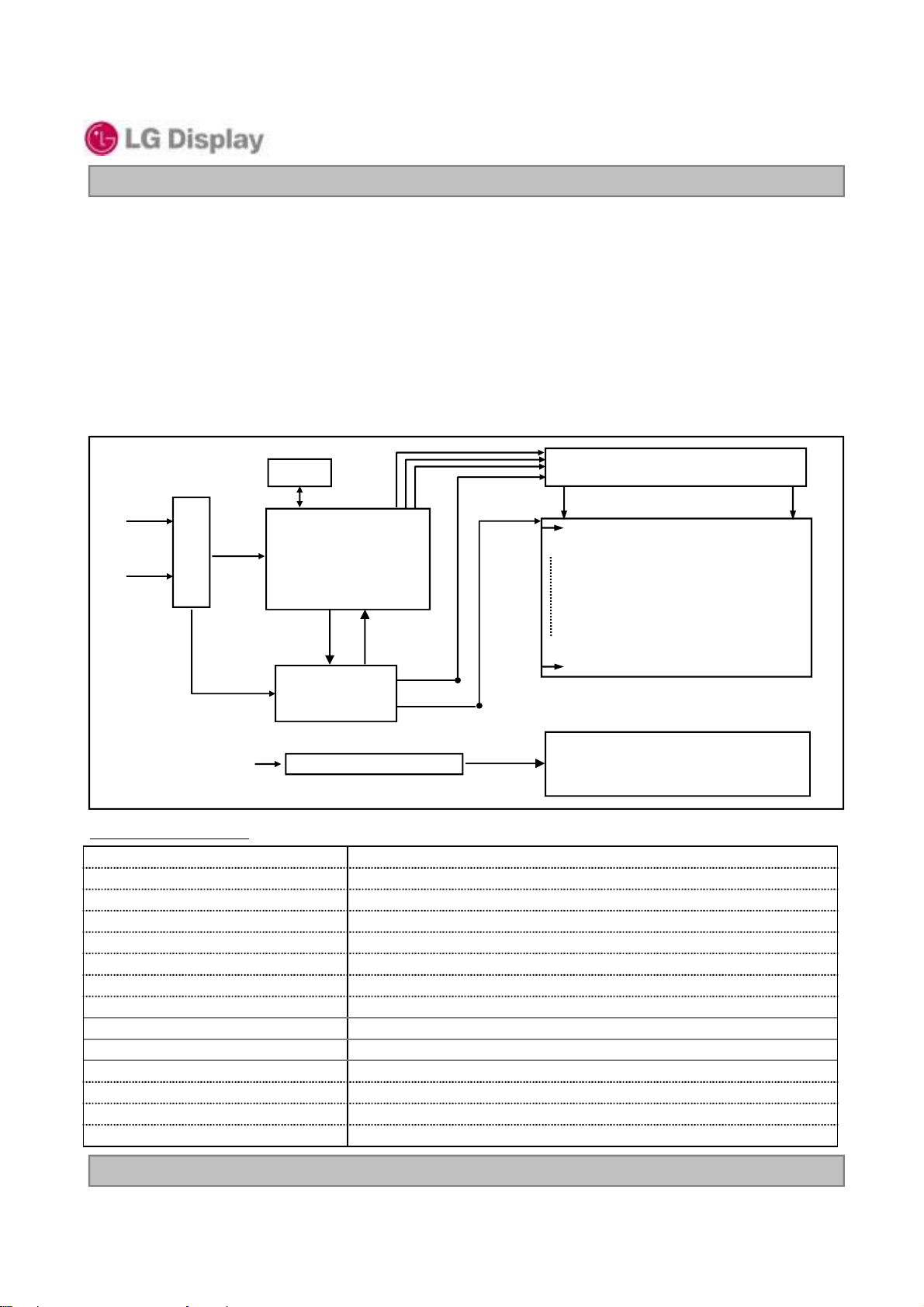
1. General Description
LM230WFA is a Color Active Matrix Liquid Crystal Display with a Light Emitting Diode ( White LED) backlight
system without LED driver. The matrix employs a-Si Thin Film Transistor as the active element.
It is a transmissive type display operating in the normally black mode. It has a 23 inch diagonally measured
ac ti ve d is p l a y ar ea w it h FH D res ol ut io n (1 0 80 ve rt ic al b y 19 20 ho ri zo nt a l p ix el a rr ay )
Each pixel is divided into Red, Green and Blue sub-pixels or dots which are arranged in vertical stripes.
Gray scale or the brightness of the sub-pixel color is determined with a 8-bit gray scale signal for each dot,
thus, presenting a palette of more than 16,7M colors with A-FRC (Advanced Frame Rate Control).
It has been designed to apply the 8Bit 2 port LVDS interface.
It i s in te n de d to s up po r t di sp la y s w he r e hi gh b ri gh t ne s s , s up er w id e vi ew i ng a ng le ,
high color saturation, and high color are important.
Mini-LVDS (RGB)
Source Driver Circuit
S1 S1920
TFT - LCD Panel
(1920 × RGB × 1080 pixels)
LVDS
2port
+5.0V
CN1
(30pin)
EEPROM
I2C
G1
Timing
Controller
Logic Power
3.3V
+5.0V
Power Circuit
Block
V
LED
General Features
Active Screen Size 23 inches(58.42cm) diagonal
Outline Dimension 533.2(H) x 312.0(V) x 11.0(D) mm (Typ.)
Pixel Pitch 0.2652 mm x 0.2652 mm
Pixel Format 1920 horiz. By 1080 vert. Pixels RGB stripes arrangement
Color Depth 16,7M colors (6bit + A-FRC)
Luminance, White 250 cd/m
Viewing Angle(CR>10) View Angle Free (R/L 178(Typ.), U/D 178(Typ.))
3D Viewing Angle(3DCT<10) R/L 65˚ / 65˚ (Typ.), U+D 12˚ (Typ.)
3D C/T (within viewing cone min.) ≤ 1.8% (Typ.)
3D Brightness (Glass trans. 00%) ≥ 95nit (Typ.)
Power Consumption Total 25.2 Watt (Typ.) ( 4.1 Watt @VLCD, 21.1 Watt @Is=110mA )
Weight 2,100g (typ.)
Display Operating Mode Transmissive mode, normally black
Surface Treatment Hard coating(3H), Anti-glare treatment of the front polarizer
CN2 (6PIN)
[ Figure 1 ] Block diagram
2
( Center 1 Point, Typ.)
Back light Assembly
(LED)
Ver. 1.0 Aug. 10 . 2011
4 / 34
Page 7
LM230WFA
Liquid Crystal Display
Product Specification
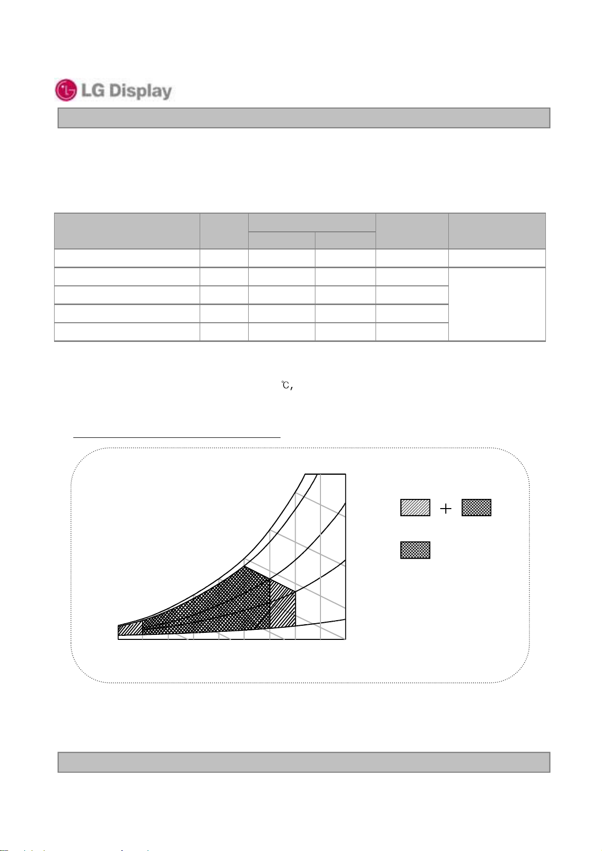
2. Absolute Maximum Ratings
The following are maximum values which, if exceeded, may cause faulty operation or damage to the unit.
Table 1. ABSOLUTE MAXIMUM RATINGS
Parameter Symbol
Power Input Voltage
Operating Temperature
Storage Temperature
Operating Ambient Humidity
Storage Humidity
VLCD -0.3 6.0 Vdc
TOP 0 50
TST -20 60
HOP 10 90 %RH
HST 10 90 %RH
Values
Units Notes
Min Max
°C
°C
Note : 1. Temperature and relative humidity range are shown in the figure below.
Wet bulb temperature should be 39 °C Max, and no condensation of water.
2. Maximum Storage Humidity is up to 40℃, 70% RH only for 4 corner light leakage Mura.
3. Storage condition is guaranteed under packing condition
FIG.2 Temperature and relative humidity
90%
60
60%
at 25 ± 2°C
1, 2, 3
Wet Bulb
50
Temperature [C]
40
30
20
10
0
10 20 30 40 50 60 70 800-20
Dry Bulb Temperature [C]
Ver. 1.0 Aug. 10 . 2011
40%
10%
Storage
Operation
Humidity [(%)RH]
5 / 34
Page 8
LM230WFA
Rush current
I
RUSH
--3.0
A
4
Liquid Crystal Display
Product Specification
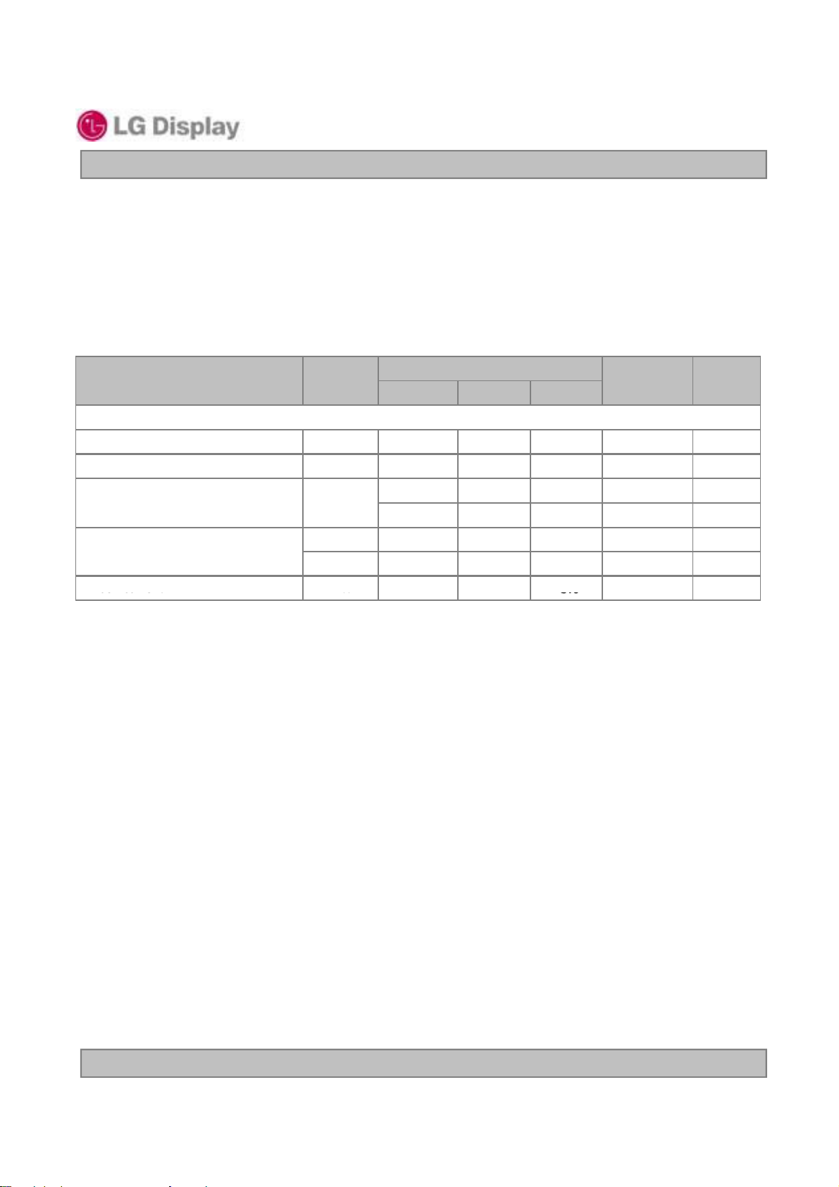
3. Electrical Specifications
3-1. Electrical Characteristics
It requires two power inputs. One is employed to power the LCD electronics and to drive the TFT array and
liquid crystal. The second input power for the LED/Backlight, is typically generated by a LED Driver.
The LED Driver is an external unit to the LCDs.
Table 2-1. ELECTRICAL CHARACTERISTICS
Parameter Symbol
MODULE :
Power Supply Input Voltage VLCD
Permissive Power Input Ripple VdRF
Power Supply Input Current ILCD
Pc TYP
Power Consumption
Pc MAX
Min Typ Max
4.5 5 5.5
- 810 930
- 910 1045
- 4.1 4.7
- 4.6 5.3
Values
400
Unit Notes
Vdc
mVp-p 1
mA 2
mA 3
Watt 2
Watt 3
Note :
1. Permissive power ripple should be measured under V
=5.0V, 25°C, fV(frame frequency)=MAX
LCD
condition and At that time, we recommend the bandwidth configuration of oscilloscope is to be under
20Mhz. See the next page.
2. The specified current and power consumption are under the VLCD=5.0V, 25± 2°C,fV=60Hz condition
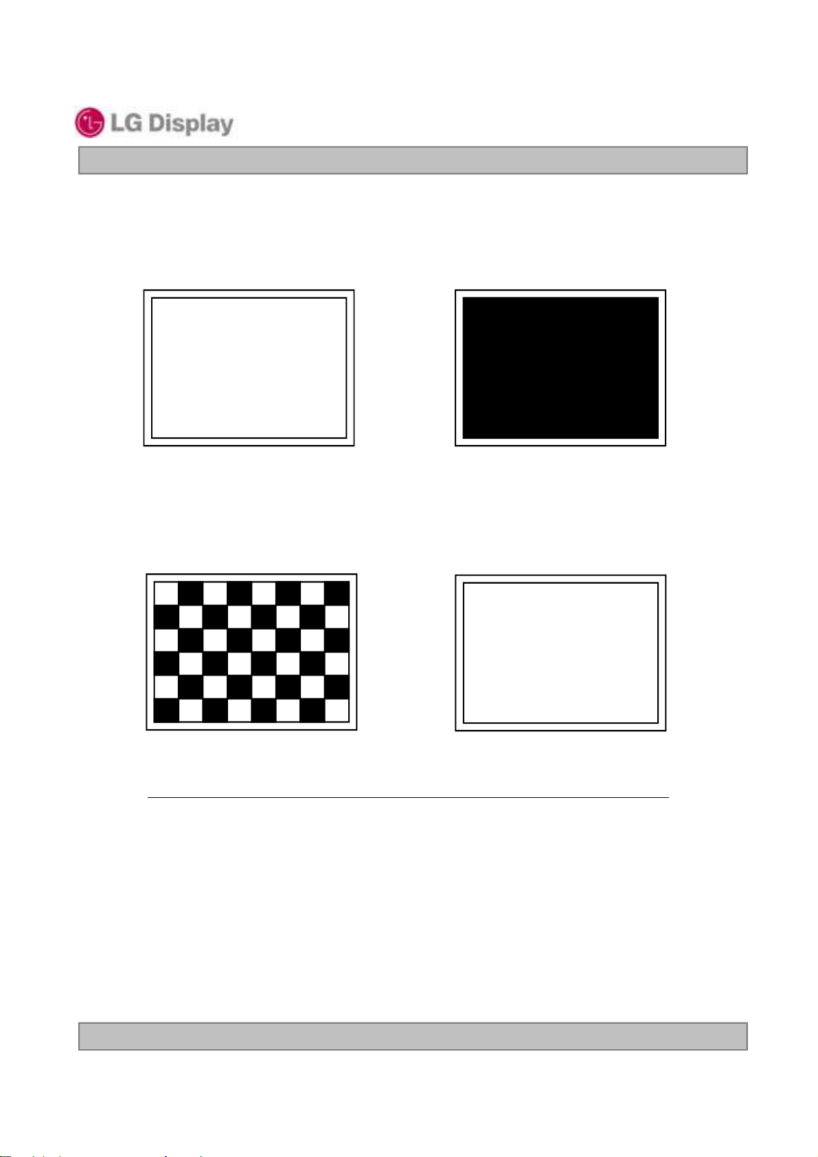
whereas Typical Power Pattern [Mosaic] shown in the [ Figure 3 ] is displayed.
3. The current is specified at the maximum current pattern.
4. Maximum Condition of Inrush current :
The duration of rush current is about 5ms and rising time of power Input is 500us ± 20%.(min.).
Ver. 1.0 Aug. 10 . 2011
6 / 34
Page 9
Product Specification
LM230WFA
Liquid Crystal Display
• Permissive Power input ripple (V
White pattern
• Power consumption (V
=5V, 25°C, fV (frame frequency=60Hz condition)
LCD
=5.0V, 25°C, fv (frame frequency)=MAX condition)
LCD
Black pattern
Typical power Pattern
FIG.3 Mosaic pattern & White Pattern for power consumption measurement
Ver. 1.0 Aug. 10 . 2011
Maximum power Pattern
7 / 34
Page 10
Product Specification
Please control feedback current of each string individually to compensate the current variation
Table 2-2. LED Bar ELECTRICAL CHARACTERISTICS
LM230WFA
Liquid Crystal Display
Parameter Symbol Condition
LED : 1,7
LED String Current Is - 110 120 mA 2,7
LED String Voltage Vs 45 48 51 V 3,7
Power Consumption
LED Life Time LED_LT 30,000 - - Hrs 5,7
PBar 19.80 21.12 22.44 Watt 4,6,7
Min. Typ. Max.
Values
Unit Notes
LED driver design guide
: The design of the LED driver must have specifications for the LED in LCD Assembly.
The performance of the LED in LCM, for example life time or brightness, is extremely influenced by
the characteristics of the LED driver.
So all the parameters of an LED driver should be carefully designed and output current should be
Constant current control.
among the strings of LEDs.
When you design or order the LED driver, please make sure unwanted lighting caused by
the mismatch of the LED and the LED driver (no lighting, flicker, etc) never occurs.
When you confirm it, the LCD module should be operated in the same condition as installed in
your instrument.
1. Specified values are for a single LED bar.
2. The specified current is input LED chip 100% duty current.
3. The specified voltage is input LED string and Bar voltage at typical 110 mA 100% duty current.
4. The specified power consumption is input LED bar power consumption at typical 110 mA 100% duty current.
5. The life is determined as the time at which luminance of the LED is 50% compared to that of initial
value at the typical LED current on condition of continuous operating at 25 ± 2°C.
6. The LED bar power consumption shown above does not include loss of external driver.
The used LED bar current is the LED typical current.
Min Power Consumption is calculated with PBar = Vs(Min.) x Is(Typ.) x Nstring
Max Power Consumption is calculated with PBar = Vbar(Max.) x Is(Typ) x Nstring
7. LED operating DC Forward Current must not exceed LED Max Ratings at 25 ± 2°C
Ver. 1.0 Aug. 10 . 2011
8 / 34
Page 11
Liquid Crystal Display
9
FCLKINP
Plus signal of odd clock channel (LVDS)
24
GND
Ground
Product Specification
3-2. Interface Connections
3-2-1. LCD Module
- LCD Connector(CN1) : IS100-L30O-C23 (UJU) , GT103-30S-HF15 (LSM)
- Mating Connector : FI-X30C2L (Manufactured by JAE) or Equivalent
Table 3. MODULE CONNECTOR(CN1) PIN CONFIGURATION
No Symbol Description No Symbol Symbol
LM230WFA
1
2
3
4
5
6
7
8
10
11
12
13
14
15
FR0M
FR0P
FR1M
FR1P
FR2M
FR2P
GND
FCLKINM
FR3M
FR3P
SR0M
SR0P
GND
SR1M
Minus signal of odd channel 0 (LVDS)
Plus signal of odd channel 0 (LVDS)
Minus signal of odd channel 1 (LVDS)
Plus signal of odd channel 1 (LVDS)
Minus signal of odd channel 2 (LVDS)
Plus signal of odd channel 2 (LVDS)
Ground
Minus signal of odd clock channel (LVDS)
Minus signal of odd channel 3 (LVDS)
Plus signal of odd channel 3 (LVDS)
Minus signal of even channel 0 (LVDS)
Plus signal of even channel 0 (LVDS)
Ground
Minus signal of even channel 1 (LVDS)
16
SR1P
17
GND
18
SR2M
19
SR2P
20
SCLKINM
21
SCLKINP
22
SR3M
23
SR3P
25
NC
26
NC
PWM_OUT For Control Burst frequency of Inverter
27
28
VLCD
29
VLCD
30
VLCD
Plus signal of even channel 1 (LVDS)
Ground
Minus signal of even channel 2 (LVDS)
Plus signal of even channel 2 (LVDS)
Minus signal of even clock channel (LVDS)
Plus signal of even clock channel (LVDS)
Minus signal of even channel 3 (LVDS)
Plus signal of even channel 3 (LVDS)
No Connection (I2C Serial interface for LCM)
No Connection.(I2C Serial interface for LCM)
Power Supply +5.0V
Power Supply +5.0V
Power Supply +5.0V
Note: 1. All GND(ground) pins should be connected together and to Vss which should also be connected to
the LCD’s metal frame.
2. All VLCD (power input) pins should be connected together.
3. Input Level of LVDS signal is based on the IEA 664 Standard.
4. PWM_OUT signal controls the burst frequency of a inverter.
This signal is synchronized with vertical frequency.
It’s frequency is 3 times of vertical frequency, and it’s duty ratio is 50%.
If you don’t use this pin, it is no connection.
IS100-L30O-C23
#1 #30
Ver. 1.0 Aug. 10 . 2011
#1
FIG.4 Connector diagram
#30
Rear view of LCM
9 / 34
Page 12
LM230WFA
13
Ground pin for TTL
GND41Positive LVDS differential data output 2
T
OUT2
+
13
Ground pin for TTL
GND41Positive LVDS differential data output 2
TXOUT2
+
Liquid Crystal Display
Product Specification
Table 4. REQUIRED SIGNAL ASSIGNMENT FOR Flat Link (TI:SN75LVDS83) Transmitter
Pin # Require SignalPin Name Pin # Require SignalPin Name
1 Power Supply for TTL InputVCC 29 Ground pin for TTLGND
2 TTL Input (R7)D5 30 TTL Input (DE)D26
3 TTL Input (R5)D6 31 TTL Level clock InputTXCLKIN
4 TTL Input (G0)D7 32 Power Down InputPWR DWN
5 Ground pin for TTLGND 33 Ground pin for PLLPLL GND
6 TTL Input (G1)D8 34 Power Supply for PLLPLL VCC
7 TTL Input (G2)D9 35 Ground pin for PLLPLL GND
8 TTL Input (G6)D10 36 Ground pin for LVDSLVDS GND
9 Power Supply for TTL InputVCC 37 Positive LVDS differential data output 3TxOUT3
10 TTL Input (G7)D11 38 Negative LVDS differential data output 3TxOUT3
11 TTL Input (G3)D12 39 Positive LVDS differential clock outputTXCLKOUT
12 TTL Input (G4)D13 40 Negative LVDS differential clock outputTXCLKOUT
14 TTL Input (G5)D14 42 Negative LVDS differential data output 2TXOUT2
15 TTL Input (B0)D15 43 Ground pin for LVDSLVDS GND
16 TTL Input (B6)D16 44 Power Supply for LVDSLVDS VCC
17 Power Supply for TTL InputVCC 45 Positive LVDS differential data output 1TXOUT1
18 TTL Input (B7)D17
19 TTL Input (B1)D18
20 TTL Input (B2)D19
22 TTL Input (B3)D20
23 TTL Input (B4)D21
24 TTL Input (B5)D22
25 TTL Input (RSVD)D23
46 Negative LVDS differential data output 1TXOUT1
47 Positive LVDS differential data output 0TXOUT0
48 Negative LVDS differential data output 0TXOUT0
49 Ground pin for LVDSLVDS GND21 Ground pin for TTL InputGND
50 TTL Input (R6)D27
51 TTL Input (R0)D0
52 TTL Input (R1)D1
53 Ground pin for TTLGND
+
-
-
+
-
+
-
+
-
26 Power Supply for TTL InputVCC 54 TTL Input (R2)D2
Notes : 1. Refer to LVDS Transmitter Data Sheet for detail descriptions.
2. 7 means MSB and 0 means LSB at R,G,B pixel data
Ver. 1.0 Aug. 10 . 2011
55 TTL Input (R3)D327 TTL Input (HSYNC)D24
56 TTL Input (R4)D428 TTL Input (VSYNC)D25
10 / 34
Page 13

LVDS Input characteristics
LVDS Input Voltage Range
VIN0.7
1.8V-
1. DC Specification
LM230WFA
Liquid Crystal Display
Product Specification
Description Symbol Min Max Unit Notes
LVDS Differential Voltage |VID| 200 600 mV -
LVDS Common mode Voltage V
CM
1.0 1.5 V -
Change in common mode Voltage ∆VCM - 250 mV -
2. AC Specification
Tclk
LVDS Clock
LVDS Data
Description Symbol Min Max Unit Notes
LVDS Clock to Data Skew Margin
SKEW (Fclk
t
SKEW
t
1) 95 MHz > Fclk ≥85 MHz : -300 ~ +300
2) 85 MHz > Fclk ≥65 MHz : -400 ~ +400
3) 65 MHz > Fclk ≥30 MHz : -600 ~ +600
t
SKEW
t
SKEW
t
SKEW
= 1/T
clk
)
- 300 + 300 ps 95MHz > Fclk ≥ 85MHz
- 400 + 400 ps 85MHz > Fclk ≥ 65MHz
- 600 + 600 ps 65MHz > Fclk ≥ 30MHz
LVDS Clock to Clock Skew Margin
(Even to Odd)
Ver. 1.0 Aug. 10 . 2011
t
SKEW_EO
- 1/7 + 1/7 T
clk
-
11 / 34
Page 14

3. Data Format
1) LVDS 2 Port
LM230WFA
Liquid Crystal Display
Product Specification
< Clock skew margin between channel >
< LVDS Data Format >
Ver. 1.0 Aug. 10 . 2011
12 / 34
Page 15

Liquid Crystal Display
Product Specification
Table 5. BACKLIGHT CONNECTOR PIN CONFIGURATION(CN2)
The LED interface connector is a model 10019HR-H06B manufactured by YEONHO.
The pin configuration for the connector is shown in the table below.
Pin Symbol Description Notes
1 FB1 Channel1 Current Feedback
2 FB2 Channel2 Current Feedback
3 VLED LED Power Supply
4 VLED LED Power Supply
5 FB3 Channel3 Current Feedback
LM230WFA
6 FB4 Channel4 Current Feedback
#1 #6
Rear view of LCM
[ Figure 5 ] Backlight connector view
Ver. 1.0 Aug. 10 . 2011
13 / 34
Page 16

LM230WFA
Liquid Crystal Display
Product Specification
3-3. Signal Timing Specifications
This is signal timing required at the input of the TMDS transmitter. All of the interface signal timing should be
satisfied with the following specifications for it’s proper operation.
Table 6. TIMING TABLE
ITEM Symbol Min Typ Max Unit Note
DCLK
Horizontal
Vertical
Period tCLK
Frequency total tHP
Frequency fH
Blanking
valid tWH
total tVP
Frequency fV
Blanking
valid tWV
11.76 13.89 15.38
60 72 87.5
1000 1088 1120
64 66 83
40 128 160
960 960 960
1090 1100 1160
50 60 75
10 20 80
1080 1080 1080
ns
MHz
tCLK
KHz
tCLK
tCLK/2
tHP
Hz
tHP
tHP
Note:
1. DE Only mode operation. The input of Hsync & Vsync signal does not
have an effect on LCD normal operation.
2. The performance of the electro-optical characteristics may be influenced by variance of the
vertical refresh rates.
3. Horizontal period should be even.
Ver. 1.0 Aug. 10 . 2011
14 / 34
Page 17

3-4. Signal Timing Waveforms
1. DCLK , DE, DATA waveforms
LM230WFA
Liquid Crystal Display
Product Specification
DCLK
tCLK
First data
Second data
DE(Data Enable)
2. Horizontal waveform
Invalid data
Invalid data
Valid data
Pixel 0,0
Valid data
Pixel 1,0
Pixel 2,0
Pixel 3,0
tHV
Invalid data
Invalid data
tHP
DE(Data Enable)
3. Vertical waveform
tVV
tHP
DE(Data Enable)
Ver. 1.0 Aug. 10 . 2011
DE
t
VP
DE
15 / 34
Page 18

LM230WFA
Liquid Crystal Display
Product Specification
3-5. Color Input Data Reference
The Brightness of each primary color(red,green,blue) is based on the 8-bit gray scale data input for the color;
the higher the binary input, the brighter the color. The table below provides a reference for color versus data
input.
Table 7. COLOR DATA REFERENCE
Input Color Data
Basic
Color
RED
Color
Black 0 0 0 0 0 0 0 0 0 0 0 0 0 0 0 0 0 0 0 0 0 0 0 0
Red (255) 1 1 1 1 1 1 1 1 0 0 0 0 0 0 0 0 0 0 0 0 0 0 0 0
Green (255) 0 0 0 0 0 0 0 0 1 1 1 1 1 1 1 1 0 0 0 0 0 0 0 0
Blue (255) 0 0 0 0 0 0 0 0 0 0 0 0 0 0 0 0 1 1 1 1 1 1 1 1
Cyan 0 0 0 0 0 0 0 0 1 1 1 1 1 1 1 1 1 1 1 1 1 1 1 1
Magenta 1 1 1 1 1 1 1 1 0 0 0 0 0 0 0 0 1 1 1 1 1 1 1 1
Yellow 1 1 1 1 1 1 1 1 1 1 1 1 1 1 1 1 0 0 0 0 0 0 0 0
White 1 1 1 1 1 1 1 1 1 1 1 1 1 1 1 1 1 1 1 1 1 1 1 1
RED (000) Dark 0 0 0 0 0 0 0 0 0 0 0 0 0 0 0 0 0 0 0 0 0 0 0 0
RED (001) 0 0 0 0 0 0 0 1 0 0 0 0 0 0 0 0 0 0 0 0 0 0 0 0
... ... ... ...
RED (254) 1 1 1 1 1 1 1 0 0 0 0 0 0 0 0 0 0 0 0 0 0 0 0 0
RED (255) 1 1 1 1 1 1 1 1 0 0 0 0 0 0 0 0 0 0 0 0 0 0 0 0
GREEN (000) Dark 0 0 0 0 0 0 0 0 0 0 0 0 0 0 0 0 0 0 0 0 0 0 0 0
MSB LSB
R7 R6 R5 R4 R3 R2 R1 R0 G7 G6 G5 G4 G3 G2 G1 G0 B7 B6 B5 B4 B3 B2 B1 B0
RED
MSB LSB
GREEN
BLUE
MSB LSB
GREEN (001) 0 0 0 0 0 0 0 0 0 0 0 0 0 0 0 1 0 0 0 0 0 0 0 0
GREEN
GREEN (254) 0 0 0 0 0 0 0 0 1 1 1 1 1 1 1 0 0 0 0 0 0 0 0 0
GREEN (255) 0 0 0 0 0 0 0 0 1 1 1 1 1 1 1 1 0 0 0 0 0 0 0 0
BLUE (000) Dark 0 0 0 0 0 0 0 0 0 0 0 0 0 0 0 0 0 0 0 0 0 0 0 0
BLUE (001) 0 0 0 0 0 0 0 0 0 0 0 0 0 0 0 0 0 0 0 0 0 0 0 1
BLUE
BLUE (254) 0 0 0 0 0 0 0 0 0 0 0 0 0 0 0 0 1 1 1 1 1 1 1 0
BLUE (255) 0 0 0 0 0 0 0 0 0 0 0 0 0 0 0 0 1 1 1 1 1 1 1 1
... ... ... ...
... ... ... ...
Ver. 1.0 Aug. 10 . 2011
16 / 34
Page 19

3-6. Power Sequence
LM230WFA
Liquid Crystal Display
Product Specification
Power Supply For LCD
V
LCD
Interface Signal (Tx)
0V
0V
Power Supply for LED
Table 8. POWER SEQUENCE
Parameter
90%
10%
T1 T2 T5 T7
Valid Data
T3 T4
LED Off LED Off
Min Typ Max
LED On
Values
90%
10%
Units
T1 0.5 - 10 ms
T2 0.01 - 50 ms
T3 500 - - ms
T4 200 - - ms
T5 0.01 - 50 ms
T7 1000 - ms
Notes : 1. Please avoid floating state of interface signal at invalid period.
2. When the interface signal is invalid, be sure to pull down the power supply for LCD V
3. LED power must be turn on after power supply for LCD and interface signal are valid.
Ver. 1.0 Aug. 10 . 2011
to 0V.
LCD
17 / 34
Page 20

Product Specification
LM230WFA
Liquid Crystal Display
3-7. V
LCD
1) Dip condition
Power Dip Condition
t
d
FIG.6 Power dip condition
V
4.5V
3.5V
GND(ground)
LCD
2) V
<
3.5V ≤V
<
3.5V
LCD
V
-dip conditions should also follow the Power On/Off conditions for supply voltage.
LCD
4.5V , td≤20ms
LCD
Ver. 1.0 Aug. 10 . 2011
18 / 34
Page 21

LM230WFA
Min
Typ
Max
Liquid Crystal Display
Product Specification
4. Optical Specifications
Optical characteristics are determined after the unit has been ‘ON’ for approximately 30 minutes
in a dark environment at 25± 2°C. The values specified are at an approximate distance 50cm from the LCD
surface at a viewing angle of Φ and θ equal to 0 ° and aperture 1 degree.
FIG. 1 presents additional information concerning the measurement equipment and method.
PR 880 or RD 80S
or PR650
Optical Stage(x,y)
LCD Module
50cm
FIG.7 Optical Characteristic Measurement Equipment and Method
4-1. 2D Optical specifications
Table 9. OPTICAL CHARACTERISTICS
Parameter Symbol
Contrast Ratio CR 600 1000 - 1
Surface Luminance, white L
Luminance Variation
Gray To Gray T
Response Time
Gray-to-Gray
(BW)
RED Rx
Color Coordinates
[CIE1931]
(By PR650)
GREEN Gx 0.312
BLUE Bx 0.150
WHITE Wx 0.313
Color Shift
(Avg. ∆u’v’ < 0.02)
Horizontal
Vertical
Viewing Angle (CR>10)
General
GSR @ 60dgree
(Gamma shift rate)
Horizontal
Vertical
Horizontal
Vertical
WPT (White Point Tracking) - -300 G255 CCT +700 K 8
Color gamut (CG, CIE1931)
Gray Scale - 2.2 9
WH
δ
WHITE
GTG_AVR
G to G
Ry 0.330
Gy 0.623
By 0.068
Wy 0.329
θ
CST_H
θ
CST_V
θ
H
θ
V
δ
Gamma_H
δ
Gamma_V
BW
(Ta=25 °C, V
200 250 - cd/m
=5V, fV=60Hz Dclk=144MHz, IBL=110mA)
LCD
Values
Units Notes
2
75 - - % 3
- 14 25 ms 4
- 8 - ms
0.638
Typ
-0.03
- 140 -
- 100 -
170 178 170 178 -
- - 20
- - 20
-
72 - %
Typ
+0.03
Degree 5
Degree 6
% 7
Reference
2
10
Ver. 1.0 Aug. 10 . 2011
19 / 34
Page 22

Product Specification
-
Color difference (
∆u’v’)
24
LM230WFA
Liquid Crystal Display
Notes 1. Contrast Ratio(CR) is defined mathematically as :
RatioContrast =
It is measured at center point(Location P1)
2. Surface luminance(LWH)is luminance value at Center 1 point(P1) across the LCD surface 50cm
from the surface with all pixels displaying white. For more information see FIG.8 (By PR880)
3. The variation in surface luminance , δ WHITE is defined as :
=
δ
WHITE
Where L1 to L9 are the luminance with all pixels displaying white at 9 locations.
For more information see FIG.8
4. Gray to gray response time is the time required for the display to transition from gray to gray.
For additional information see Table 10.
5. Color shift is the angle at which the average color difference for all Macbeth is lower than 0.02.
For more information see FIG.9
(By EZ Contrast)
(By RD80S)
(By PR880)
…
)L .. ,L,Minimum(L
P9P2P1
×
)L .... ,L ,(L Maximum
P9P2P1
pixels whiteall with Luminance Surface
pixelsblack all with Luminance Surface
(By PR880)
100
4
'
=
u
- Pattern size : 25% Box size
- Viewing angle direction of color shift : Horizontal, Vertical
6. Viewing angle is the angle at which the contrast ratio is greater than 10. The angles are
determined for the horizontal or x axis and the vertical or y axis with respect to the z axis which
is normal to the LCD surface. For more information see FIG.10
7. GSR is the rate of gamma shift at up, down, left and right 60 degree viewing angle compare with
center gamma. For more information see FIG.11 and FIG.12
- GSR (δ
.
8. WPT (White Point Tracking) is the variation of color temperature between G255 and G63.
Gamma
1 ×
x
++−
yx
24
i
)''(
=∆
vuAvg
) is defined as :
−=GSR
'
=
3122
1∑=
v
)''(
∆
ivu
9
y
3122
++−
yx
u’1, v’1 : u’v’ value at viewing angle direction
u’2, v’2 : u’v’ value at front (θ=0)
i : Macbeth chart number (Define 23 page)
2
21
(By PR880)
(By EZ Contrast)
Degree) 60Light Reft, Down, (Up, Value Gamma angle View
Degree) (0 Value GammaCenter
100
2
)''()''('' vvuuvu −+−=∆
21
(By PR650)
Ver. 1.0 Aug. 10 . 2011
20 / 34
Page 23

LM230WFA
Liquid Crystal Display
Product Specification
Notes 9. Gamma Value is approximately 2.2. For more information see Table 11.
Notes 10. Response time is the time required for the display to transit from any gray to white (Rise Time, TrR)
and from any gray to black (Decay time, TrD).
G to GBW Spec stands for average value of all measured points.
Measuring point for surface luminance & measuring point for luminance variation.
H
(By RD80S)
H/2
●
●
P2
P5
V/2
V
●
V/10
P7
●
P3
●
P1
●
P8
●
●
●
H/10
P4
P6
P9
FIG.8 Measure Point for Luminance
The Gray to Gray response time is defined as the following figure and shall be measured by switching the input
signal for “Gray To Gray “.
- Gray step : 5 Step
- TGTG_AVR is the total average time at rising time and falling time for “Gray To Gray “.
- if system use ODC ( Over Driving Circuit) function, Gray to Gary response time may be 5ms~8ms GtG
* it depends on Overshoot rate.
Table. 10 GTG Gray Table
Rising Time
Gray to Gray
G255 G191 G127 G63 G0
Falling Time G255
G191
G127
G63
G0
Ver. 1.0 Aug. 10 . 2011
21 / 34
Page 24

LM230WFA
Liquid Crystal Display
Product Specification
G to G(BW) Response time is defined as the following figure and shall be measured by switching the input
signal for “Gray(N)” and “Black or White”.
Tr
100
90
Optical
Response
10
0
Gray(N)
White
N = 0(Black)~255(White)
Color shift is defined as the following test pattern and color.
Gray(N)
Tf
Black
25% Box size
FIG.9 Color Shift Test Pattern
Average RGB values in Bruce RGB for Macbeth Chart
Dark skin (i=1) Light skin Blue sky Foliage Blue flower Bluish green
R 98 206 85 77 129 114
G 56 142 112 102 118 199
B 45 123 161 46 185 178
Orange Purplish blue Moderate red Purple Yellow green Orange yellow
R 219 56 211 76 160 230
G 104 69 67 39 193 162
B 24 174 87 86 58 29
Blue Green Red Yellow Magenta Cyan
R 26 72 197 241 207 35
G 32 148 27 212 62 126
B 145 65 37 36 151 172
White Neutral 8 Neutral 6.5 Neutral 5 Neutral 3.5 Black
R 240 206 155 110 63 22
G 240 206 155 110 63 22
B 240 206 155 110 63 22
Ver. 1.0 Aug. 10 . 2011
22 / 34
Page 25

Dimension of viewing angle range.
+=−
LM230WFA
Liquid Crystal Display
Product Specification
φ
= 180°, Left
φ
= 270°, Down
Normal
E
θ
φ
FIG.10 Viewing angle
Y
φ
= 90°, Up
φ
= 0°, Right
FIG.11 Sample Luminance vs. gray scale
(using a 256 bit gray scale)
r
LaVL +=
b
FIG.12 Sample Log-log plot of luminance
vs. gray scale
b
)log()log()log( aVrLL
Here the Parameter α and γ relate the signal level V to the luminance L.
The GAMMA we calculate from the log-log representation (FIG.11)
Ver. 1.0 Aug. 10 . 2011
23 / 34
Page 26

Table 11. Gray Scale Specification
Gray Level Relative Luminance [%] (Typ.)
LM230WFA
Liquid Crystal Display
Product Specification
0
31 1.08
63 4.72
95 11.49
127 21.66
159 35.45
191 53.00
223 74.48
255 100
0.11
Ver. 1.0 Aug. 10 . 2011
24 / 34
Page 27

Product Specification
1Point
3D Surface Luminance, white
L
1Point
7695-
cd/m
2
3(Ref.)
4-2-1. 3D Optical Specification
LM230WFA
Liquid Crystal Display
Table 11. 3D Optical characteristics
Parameter Symbol Condition
3D Viewing Angle
y axis, up (φ=90°)
y axis, down (φ=270°)
3D Crosstalk (C/T) -
Φyu+
Φyd
Ta= 25°C, V
※
Cone angle
(3D C/T ≤ 10%)
Mid Axis
(Center of Cone
Angle)
LCD
4-2-2. 3D Optical Characteristic Reference
Table 12. 3D Optical Characteristic Ref.
Parameter Symbol Condition
WH
3D Watching Distance
Ta= 25°C, V
(3D Glasses)
Mid Axis
(Center of Cone
Angle)
=5.0V, fV=60Hz f
Values
Min Typ Max
8 12 - degree
- 1.8 3 %
=5.0V, fV=60Hz f
LCD
Values
Min Typ Max
50 70 cm
=72.0MHz, Is=110mA
CLK
Units Notes
=72.0MHz, Is=110mA
CLK
Units Notes
5
4
6(Ref.)
Notes :
In order to measure 3D viewing angle, it need to be prepared as below;
1. Measurement configuration
4-Test pattern images. Refer to FIG 14.
-. LW-RW : White for left and right eye
-. LW-RB : White for left eye and Black for right eye
-. LB-RW : Black for left eye and white for right eye
-. LB-RB : Black for left eye and right eye
Image files where black and white lines are displayed on even or odd lines.
Luminance measurement system (LMS) with narrow FOV (field of view) is used. Refer to
FIG 7.
Ver. 1.0 Aug. 10 . 2011
25 / 34
Page 28

Product Specification
Figure 14. Measurement configuration
LM230WFA
Liquid Crystal Display
LW-RW LB-RW
LW-RB
LB-RB
(a) Test pattern image
Figure 15. Positioning eyeglass
θ
2
6
7
1
3
8
Right or left eyeglass
4 5
9
3D display
( Circular polarizer )
(b) Measurement
position
(c) Setup
Figure 16. notation of luminance measurement
Luminance
Lum( LE or RE, test pattern, number )
Measurement through
Left or Right eyeglass
measurement
position
LMS
2. Positioning Eyeglass
Find angle of minimum transmittance.
This value would be provided beforehand or measured by the following steps;
(i) Test image (LB-RW) is displayed.
(ii) Left eyeglass are placed in front of LMS and luminance is measured,
rotating right eyeglass such as FIG 15. The notation for luminance measurement is
“Lum(LE, LB-RW,1)”.
(iii) Find the angle where luminance is minimum.
* Following measurements should be performed at the angle of minimum transmittance of
eyeglass.
Ver. 1.0 Aug. 10 . 2011
26 / 34
Page 29

Product Specification
(iii) The 3D crosstalk (min.) is minimum 3D crosstalk within viewing angle.
3. Measurement of 3D luminance (Reference)
(i) Test image ( LW-RW ) is displayed.
(ii) Left or right eyeglass are placed in front of LMS successively and
luminance is measured at center 1 point where the notation for luminance measurement
is “Lum(LE, LW-RW,1)” or “Lum(RE, LW-RW,1).
4. Measurement of 3D crosstalk
(i) Test image ( LB-RW, LW-RB and LB-RB ) is displayed.
(ii) Right or left eyeglass are placed in front of LMS successively and
luminance is measured for position 1.
with rotating LMS or sample vertically.
Average of
Lum(LE, LB-RW,1) - Lum(LE, LB-RB,1)
LM230WFA
Liquid Crystal Display
and
5. Measurement of 3D Viewing Angle
3D viewing angle is the angle at which the 3D crosstalk is under 10%. The angles are
determined for the vertical or y axis with respect to the z axis which is normal to the LCD
module surface and measured for position 1. The typical center of U/D viewing angle is 2˚
(Φyu(up)) direction. For more information , see the Fig 17.
Lum(LE, LW-RB,1) - Lum(LE, LB-RB,1)
Lum(RE, LW-RB,1) - Lum(RE, LB-RB,1)
Lum(RE, LB-RW,1) - Lum(RE, LB-RB,1)
Ver. 1.0 Aug. 10 . 2011
27 / 34
Page 30

Product Specification
Figure 17. Measurement of 3D crosstalk and 3D viewing angle
y axis
LM230WFA
Liquid Crystal Display
LB-RW LW-RB
LCM
Φyu(up)
Φyd (down)
z axis
LB-RB
(a) Test pattern image
(b) Measurement of 3D viewing angle (up/down)
6. 3D Watching Distance (Reference)
FPR 3D Watching distance is 3D operating distance which has the range of under 10%
Cross talk of front panel from center (Mid Axis).
Figure 18. 3D Watching Distance
P
F
a
P
n
R
e
l
C/F Glass
3D Watching area
LMS
1V (A/A )
Viewing height (0.5H)
Min. Distance (500mm)
Space
Optimum Distance (700mm)
Ver. 1.0 Aug. 10 . 2011
28 / 34
Page 31

LM230WFA
Liquid Crystal Display
Product Specification
5. Mechanical Characteristics
The contents provide general mechanical characteristics. In addition the figures in the next page are detailed
mechanical drawing of the LCD.
Horizontal 533.2mm
Outline Dimension
Bezel Area
Active Display Area
Weight Typ : 2,100g , Max : 2,200g
Surface Treatment Anti-glare treatment of the front polarizer
Vertical 312.0mm
Depth 11.0 mm
Horizontal 513.2mm
Vertical 290.4mm
Horizontal 509.184mm
Vertical 286.416mm
Notes : Please refer to a mechanic drawing in terms of tolerance at the next page.
Ver. 1.0 Aug. 10 . 2011
29 / 34
Page 32

<FRONT VIEW>
LM230WFA
Liquid Crystal Display
Product Specification
Ver. 1.0 Aug. 10 . 2011
30 / 34
Page 33

<REAR VIEW>
LM230WFA
Liquid Crystal Display
Product Specification
LGD Highly recommendation :
As The IPS panel is sensitive & slim, please recommend the metal frame of the system supports the panel
by the double side-mount.
Ver. 1.0 Aug. 10 . 2011
31 / 34
Page 34

Product Specification
One time each direction
6. Reliability
Environment test condition
No Test Item Condition
1 High temperature storage test Ta= 60°C 240h
2 Low temperature storage test Ta= -20°C 240h
3 High temperature operation test Ta= 50°C 50%RH 240h
4 Low temperature operation test Ta= 0°C 240h
Wave form : random
5
Vibration test
(non-operating)
Vibration level : 1.00G RMS
Bandwidth : 10-300Hz
Duration : X, Y, Z, 10 min
One time each direction
LM230WFA
Liquid Crystal Display
Shock level : 100G
6
7 Humidity condition Operation Ta= 40 °C ,90%RH
8
9
Shock test
(non-operating)
Altitude
operating
storage / shipment
Maximum Storage Humidity for
4 corner light leakage Mura.
Waveform : half sine wave, 2ms
Direction :±X, ±Y, ±Z
0 - 10,000 feet(3,048m)
0 - 40,000 feet(12,192m)
Max 70%RH , Ta=40
℃
Ver. 1.0 Aug. 10 . 2011
32 / 34
Page 35

LM230WFA
Class 1M laser (LEDs) radiation when open.
Liquid Crystal Display
Product Specification
7. International Standards
7-1. Safety
a) UL 60950-1, Second Edition, Underwriters Laboratories Inc.
Information Technology Equipment - Safety - Part 1 : General Requirements.
b) CAN/CSA C22.2 No.60950-1-07, Second Edition, Canadian Standards Association.
Information Technology Equipment - Safety - Part 1 : General Requirements.
c) EN 60950-1:2006 + A11:2009, European Committee for Electrotechnical Standardization(CENELEC).
Information Technology Equipment - Safety - Part 1 : General Requirements.
d) IEC 60950-1:2005, Second Edition, The International Electrotechnical Commission (IEC).
Information Technology Equipment - Safety - Part 1 : General Requirements.
(Including report of IEC60825-1:2001 clause 8 and clause 9)
Notes
1. Laser (LED Backlight) Information
Class 1M LED Product
IEC60825-1 : 2001
Embedded LED Power (Class 1M)
2. Caution
: LED inside.
Do not open while operating.
7-2. EMC
a) ANSI C63.4 “American National Standard for Methods of Measurement of Radio-Noise
Emissions from Low-Voltage Electrical and Electronic Equipment in the Range of 9 kHz to 40 GHz.”
American National Standards Institute (ANSI), 2003.
b) CISPR 22 “Information technology equipment – Radio disturbance characteristics – Limit and
methods of measurement." International Special Committee on Radio Interference
(CISPR), 2005.
c) CISPR 13 “Sound and television broadcast receivers and associated equipment – Radio disturbance
characteristics – Limits and method of measurement." International Special Committee on Radio
Interference (CISPR), 2006.
7-3. Environment
a) RoHS, Directive 2002/95/EC of the European Parliament and of the council of 27 January 2003
Ver. 1.0 Aug. 10 . 2011
33 / 34
Page 36

Product Specification
B
MarkA678945C32
1
8. Packing
8-1. Designation of Lot Mark
a) Lot Mark
A B C D E F G H I J K L M
A,B,C : SIZE(INCH) D : YEAR
E : MONTH F ~ M : SERIAL NO.
Note
1. YEAR
LM230WFA
Liquid Crystal Display
Year
Mark
CBA
2014E2015
D
201320122011
2016G2017H2018J2019
F
2. MONTH
Month
Apr
May
Jun
Jul
Aug
Sep
b) Location of Lot Mark
Serial No. is printed on the label. The label is attached to the backside of the LCD module.
This is subject to change without prior notice.
8-2. Packing Form
a) Package quantity in one box : 11pcs
b) Box Size : 408 x 355 x 600
2020
K
Oct
Nov
DecMarFebJan
Ver. 1.0 Aug. 10 . 2011
34 / 34
Page 37

LM230WFA
chemical damage to the polarizer.
Liquid Crystal Display
Product Specification
9. PRECAUTIONS
Please pay attention to the followings when you use this TFT LCD module.
9-1. MOUNTING PRECAUTIONS
(1) You must mount a module using holes arranged in four corners or four sides.
(2) You should consider the mounting structure so that uneven force (ex. Twisted stress) is not applied to the
module. And the case on which a module is mounted should have sufficient strength so that external
force is not transmitted directly to the module.
(3) Please attach the surface transparent protective plate to the surface in order to protect the polarizer.
Transparent protective plate should have sufficient strength in order to the resist external force.
(4) You should adopt radiation structure to satisfy the temperature specification.
(5) Acetic acid type and chlorine type materials for the cover case are not desirable because the former
generates corrosive gas of attacking the polarizer at high temperature and the latter causes circuit break
by electro-chemical reaction.
(6) Do not touch, push or rub the exposed polarizers with glass, tweezers or anything harder than HB
pencil lead. And please do not rub with dust clothes with chemical treatment.
Do not touch the surface of polarizer for bare hand or greasy cloth.(Some cosmetics are detrimental
to the polarizer.)
(7) When the surface becomes dusty, please wipe gently with absorbent cotton or other soft materials like
chamois soaks with petroleum benzene. Normal-hexane is recommended for cleaning the adhesives
used to attach front / rear polarizers. Do not use acetone, toluene and alcohol because they cause
(8) Wipe off saliva or water drops as soon as possible. Their long time contact with polarizer causes
deformations and color fading.
(9) Do not open the case because inside circuits do not have sufficient strength.
(10) As The IPS panel is sensitive & slim, please recommend the metal frame of the system supports the panel
by the double side-mount.
9-2. OPERATING PRECAUTIONS
(1) The spike noise causes the mis-operation of circuits. It should be lower than following voltage :
V=± 200mV(Over and under shoot voltage)
(2) Response time depends on the temperature.(In lower temperature, it becomes longer.)
(3) Brightness depends on the temperature. (In lower temperature, it becomes lower.)
And in lower temperature, response time(required time that brightness is stable after turned on) becomes
longer.
(4) Be careful for condensation at sudden temperature change. Condensation makes damage to polarizer or
electrical contacted parts. And after fading condensation, smear or spot will occur.
(5) When fixed patterns are displayed for a long time, remnant image is likely to occur.
(6) Module has high frequency circuits. Sufficient suppression to the electromagnetic interference shall be
done by system manufacturers. Grounding and shielding methods may be important to minimized the
interference.
(7) Please do not give any mechanical and/or acoustical impact to LCM. Otherwise, LCM can’t be operated
its full characteristics perfectly.
(8) A screw which is fastened up the steels should be a machine screw.
(if not, it causes metallic foreign material and deal LCM a fatal blow)
(9) Please do not set LCD on its edge.
(10) When LCMs are used for public display defects such as Yogore, image sticking can not be guarantee.
Ver. 1.0 Aug. 10 . 2011
35 / 34
Page 38

LM230WFA
This should be peeled off slowly and carefully by people who are electrically grounded and with well ion
-
Liquid Crystal Display
Product Specification
9-3. ELECTROSTATIC DISCHARGE CONTROL
Since a module is composed of electronic circuits, it is not strong to electrostatic discharge. Make certain that
treatment persons are connected to ground through wrist band etc. And don’t touch interface pin directly.
9-4. PRECAUTIONS FOR STRONG LIGHT EXPOSURE
Strong light exposure causes degradation of polarizer and color filter.
9-5. STORAGE
When storing modules as spares for a long time, the following precautions are necessary.
(1) Store them in a dark place. Do not expose the module to sunlight or fluorescent light. Keep the temperature
between 5°C and 35°C at normal humidity.
(2) The polarizer surface should not come in contact with any other object.
It is recommended that they be stored in the container in which they were shipped.
9-6. HANDLING PRECAUTIONS FOR PROTECTION FILM
(1) The protection film is attached to the bezel with a small masking tape.
When the protection film is peeled off, static electricity is generated between the film and polarizer.
blown equipment or in such a condition, etc.
(2) When the module with protection film attached is stored for a long time, sometimes there remains a very
small amount of glue still on the bezel after the protection film is peeled off.
(3) You can remove the glue easily. When the glue remains on the bezel surface or its vestige is recognized,
please wipe them off with absorbent cotton waste or other soft material like chamois soaked with normalhexane.
Ver. 1.0 Aug. 10 . 2011
36 / 34
 Loading...