LG Display LD420WUB-SCB1 Specification
Global LCD Panel Exchange Center
www.panelook.com
One step solution for LCD / PDP / OLED panel application: Datasheet, inventory and accessory!
www.panelook.com
LD420WUB
Product Specification
SPECIFICATION
FOR
APPROVAL
)
(
Preliminary Specification
)
(
Final Specification
●
MODEL
APPROVED BY
/
/
GeneralBUYER
SIGNATURE
DATE
42.0” WUXGA TFT LCDTitle
LG DISPLAY Co., Ltd.SUPPLIER
LD420WUB*MODEL
SCB1(RoHS Verified)SUFFIX
*When you obtain standard approval,
please use the above model name without suffix
APPROVED BY
K.S. Nah
/ Chief Research Engineer
REVIEWED BY
M. G. Lee
/ Senior Engineer
SIGNATURE
DATE
PREPARED BY
J. H. Kim
/
Please return 1 copy for your confirmation with
your signature and comments.
Ver1.0
/ Junior Engineer
PD Design Team
LG Display Co., Ltd.
1 / 35
Global LCD Panel Exchange Center
www.panelook.com
One step solution for LCD / PDP / OLED panel application: Datasheet, inventory and accessory!
www.panelook.com
LD420WUB
Product Specification
CONTENTS
CONTENTS
RECORD OF REVISIONS
GENERAL DESCRIPTION1
ABSOLUTE MAXIMUM RATINGS2
ELECTRICAL SPECIFICATIONS3
ELECTRICAL CHARACTERISTICS3-1
INTERFACE CONNECTIONS3-2
SIGNAL TIMING SPECIFICATIONS3-3
SIGNAL TIMING WAVEFORMS3-4
COLOR DATA REFERENCE3-5
POWER SEQUENCE3-6
OPTICAL SPECIFICATIONS4
MECHANICAL CHARACTERISTICS5
ITEMNumber
Page
1COVER
2
3
4
5
6
6
8
10
11
14
15
17
21
Ver1.0
RELIABILITY6
INTERNATIONAL STANDARDS7
SAFETY7-1
EMC7-2
PACKING8
INFORMATION OF LCM LABEL8-1
PACKING FORM8-2
PRECAUTIONS9
MOUNTING PRECAUTIONS9-1
OPERATING PRECAUTIONS9-2
ELECTROSTATIC DISCHARGE CONTROL9-3
PRECAUTIONS FOR STRONG LIGHT EXPOSURE9-4
STORAGE9-5
HANDLING PRECAUTIONS FOR PROTECTION FILM9-6
APPROPRIATE CONDITION FOR PUBLIC DISPLAY9-7
24
25
25
25
26
26
26
27
27
27
28
28
28
28
28
2 / 35
Global LCD Panel Exchange Center
www.panelook.com
One step solution for LCD / PDP / OLED panel application: Datasheet, inventory and accessory!
www.panelook.com
LD420WUB
Product Specification
RECORD OF REVISIONS
DescriptionPageRevision DateRevision No.
Preliminary Specification-July. 19. 20100.0
Table 11. OPTICAL CHARACTERISTICS17Oct. 05. 20100.1
Defined CR Spec for Min. value17Nov. 26. 2010
Final Specification-Nov. 26. 20101.0
Ver1.0
3 / 35
Global LCD Panel Exchange Center
www.panelook.com
One step solution for LCD / PDP / OLED panel application: Datasheet, inventory and accessory!
www.panelook.com
1. General Description
LD420WUB is a Color Active Matrix Liquid Crystal Display with an integral Cold Cathode Fluorescent
Lamp(CCFL) backlight system. The matrix employs a-Si Thin Film Transistor as the active element.
It is a transmissive type display operating in the normally black mode. It has a 42 inch diagonally measured
act i ve d is p la y area w i th W U X GA res o l u t io n (1080 ve rtical b y 1920 horizontal pixel ar ray)
Each pixel is divided into Red, Green and Blue sub-pixels or dots which are arranged in vertical stripes.
Gray scale or the luminance of the sub-pixel color is determined with a 8bit or 10-bit gray scale signal for
each dot, thus presenting a palette of more than 1.06Billion of colors.
It has been designed to apply the 10-bit 2 port LVDS interface.
It is intended to support Public Display where high brightness, super wide viewing angle, high color gamut,
high color depth and fast moving picture response time are important.
LD420WUB
Product Specification
LVDS
2Port
LVDS
Select
Bit
Select
+12.0V
VBR-A, VBR-B
LVDS 1,2
Option
signal
CN1
(51pin)
I2C
Status
+24.0V, GND
General Features
EEPROM
SCL
Timing Controller
LVDS Rx + DGA + ODC
Power Circuit
SDA
Integrated
Block
Inverter
42.02 inches(1067.31mm) diagonalActive Screen Size
956.4(H) x 549.4 (V) x 53.5 mm(D) (Typ.)Outline Dimension
0.4845 mm x 0.4845 mmPixel Pitch
1920 horiz. by 1080 vert. Pixels, RGB stripe arrangementPixel Format
10bit (D) , 1.06Billon colorsColor Depth
500 cd/m2 (Center 1point ,Typ.)Luminance, White
Viewing angle free ( R/L 178 (Typ.), U/D 178 (Typ.))Viewing Angle (CR>10)
Mini-LVDS(RGB)
Control
Signals
Power Signals
3PinX1CN(High)
3PinX1CN(High)
Source Driver Circuit
S1 S1920
G1
TFT - LCD Panel
(1920 × RGB × 1080 pixels)
[Gate In Panel]
G1080
Back light Assembly
Total 175.8 W (Typ.) (Logic = 7.8W, Inverter = 168W [VBR-A=1.65V] ) Power Consumption
10.5Kg (Typ.)Weight
Transmissive mode, Normally blackDisplay Mode
Hard coating(3H), Advanced glare treatment of the front polarizer(Haze10%)Surface Treatment
Landscape and Portrait Enabled Possible Display Type
Ver1.0
4 / 35
Global LCD Panel Exchange Center
www.panelook.com
One step solution for LCD / PDP / OLED panel application: Datasheet, inventory and accessory!
www.panelook.com
2. Absolute Maximum Ratings
The following items are maximum values which, if exceeded, may cause faulty operation or damage to the
LCD module.
Table 1. ABSOLUTE MAXIMUM RATINGS
Parameter Remark
Symbol
LD420WUB
Product Specification
Value
Unit
MaxMin
Power
Input
Voltage
Notes
LCM
+500TOPOperating Temperature
+60-20TSTStorage Temperature
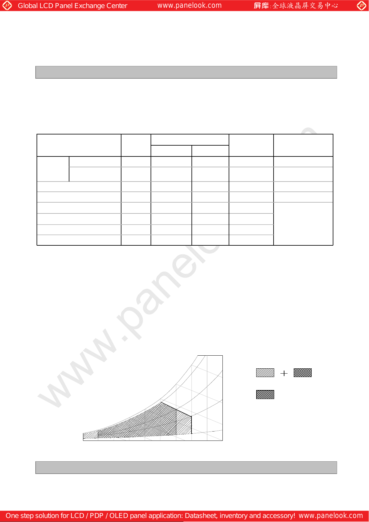
1. Ambient temperature condition (Ta = 25 ± 2 °C )
2. Temperature and relative humidity range are shown in the figure below.
Wet bulb temperature should be Max 39°C, and no condensation of water.
at 25 ± 2 °CVDC+14.0-0.3VLCD
VDC+27.0-0.3VBLBacklight inverter
VDC+5. 5-0.3VON/OFFON/OFF Control Voltage
VDC+5.00VBRBrightness Control Voltage
°C
°C
%RH9010HOPOperating Ambient Humidity
%RH9010HSTStorage Humidity
Note 1
90%
60
60%
Ver1.0
Wet Bulb
Temperature [C]
10
0
10 20 30 40 50 60 70 800-20
Dry Bulb Temperature [C]
20
30
40
50
40%
10%
Humidity
[(%)RH]
Storage
Operation
5 / 35
Global LCD Panel Exchange Center
www.panelook.com
One step solution for LCD / PDP / OLED panel application: Datasheet, inventory and accessory!
www.panelook.com
3. Electrical Specifications
3-1. Electrical Characteristics
It requires two power inputs. One is employed to power for the LCD circuit. The other Is used for the CCFL
backlight and inverter circuit.
Table 2. ELECTRICAL CHARACTERISTICS
Parameter Symbol
LD420WUB
Product Specification
Value
NoteUnit
MaxTypMin
Circuit :
ILCDPower Input Current
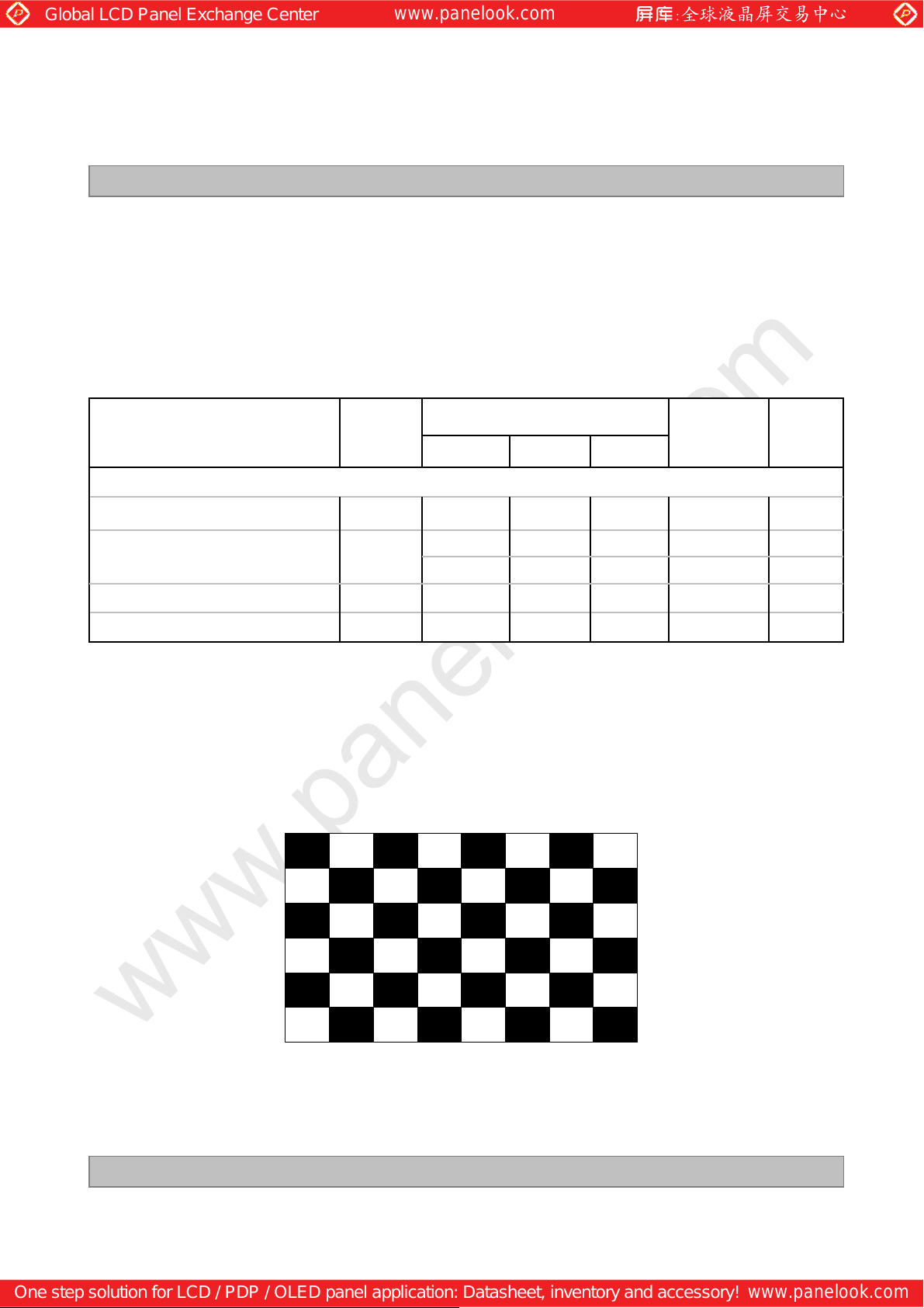
Notes : 1. The specified current and power consumption are under the V
condition whereas mosaic pattern(8 x 6) is displayed and fVis the frame frequency.
2. The current is specified at the maximum current pattern.
3. The duration of rush current is about 2ms and rising time of power input is 0.5ms (min)
White : 1023Gray
Black : 0Gray
VDC12.612.011.4VLCDPower Input Voltage
=12.0V, 25 ± 2°C, fV=60Hz
LCD
1mA728560392
2mA1072825577
1Watt10.17.8PLCDPower Consumption
3A5.0--IRUSHRush current
Mosaic Pattern(8 x 6)
Ver1.0
6 / 35
Global LCD Panel Exchange Center
www.panelook.com
One step solution for LCD / PDP / OLED panel application: Datasheet, inventory and accessory!
www.panelook.com
Table 3. ELECTRICAL CHARACTERISTICS (Continue)Table 3. ELECTRICAL CHARACTERISTICS (Continue)
LD420WUB
Product Specification
Parameter Symbol
Values
MaxTypMin
NotesUnit
Inverter :
Power Supply Input Voltage
Power Supply Input Voltage Ripple
Power Supply
Input Current
After Aging
Before Aging
Power Supply Input Current (In-Rush)
Power Consumption
Brightness Adjust
Input Voltage for
Control System
On/Off
Signals
Brightness Adjust
On
Off
IBL_A
IBL_B
VBR-A
VBR-B
Vdc25.224.022.8VBL
A12.0--Irush
Vdc3.31.650.0
Vdc5.0-2.5V on
Vdc0.80.0-0.3V off
V3.3-0
V
BR-A
V
BR-A
V
BR-A
V
BR-A
VBL= 22.8V
V
BR-B
V
BR-A
V
BR-A
7-
7.4-
8.5-
9.5-
-PBL
8
8.4
9.5
10.5
192168
1
1Vp-p0.5--
= 1.65V … 1A
= 3.3V … 1A
= 1.65V … 2A
= 3.3V … 2A
= 3.3V
= 1.65V
= 1.65V … 1W
Lamp:
Discharge Stabilization Time
Life Time
3min3TS
4Hrs50,000
Notes :
1. Electrical characteristics are determined after the unit has been ‘ON’ and stable for approximately 120
minutes at 25±2°C. The specified current and power consumption are under the typical supply Input voltage
24Vand VBR (VBR-A : 1.65V & VBR-B : 3.3V), it is total power consumption.
The ripple voltage of the power supply input voltage is under 0.5 Vp-p. LGD recommend Input Voltage is
24.0V ± 5%.
2. Electrical characteristics are determined within 30 minutes at 25±2°C.
The specified currents are under the typical supply Input voltage 24V.
3. The brightness of the lamp after lighted for 5minutes is defined as 100%.
TS is the time required for the brightness of the center of the lamp to be not less than 95% at typical current.
The screen of LCD module may be partially dark by the time the brightness of lamp is stable after turn on.
4. Specified Values are for a single lamp which is aligned horizontally.
The life time is determined as the time which luminance of the lamp is 50% compared to that of initial value
at the typical lamp current (VBR-A : 1.65V & VBR-B : 3.3V), on condition of continuous operating at 25± 2°C
5. The duration of rush current is about 20ms.
Ver1.0
7 / 35
Global LCD Panel Exchange Center
www.panelook.com
One step solution for LCD / PDP / OLED panel application: Datasheet, inventory and accessory!
www.panelook.com
3-2. Interface Connections
This LCD module employs two kinds of interface connection, a 51-pin connector is used for the module
electronics and Master 14-pin and Slave 12-pin connectors are used for the integral backlight system.
3-2-1. LCD Module
- LCD Connector(CN1): FI-R51S-HF(manufactured by JAE) or KN25-51P-0.5SH(manufactured by Hirose)
- Mating Connector : FI-R51HL(JAE) or compatible
Table 4. MODULE CONNECTOR(CN1) PIN CONFIGURATION
LD420WUB
Product Specification
10
11
12
13
14
15
16
17
18
19
20
21
22
23
24
25
26
DescriptionSymbolNo
1
2
3
4
5
6
7
8
9
GND
GND
RO0N
RO0P
RO1N
RO1P
RO2N
RO2P
GND
ROCLKN
ROCLKP
GND
RO3N
RO3P
RO4N
RO4P
Reserved
FIRST CLOCK CHANNEL C-
FIRST CLOCK CHANNEL C+
FIRST CHANNEL 4- (For 10bit D)
FIRST CHANNEL 4+ (For 10bit D)
Ground
No ConnectionNC
No ConnectionNC
No ConnectionNC
No ConnectionNC
No ConnectionNC
‘H’ =JEIDA , ‘L’ = VESA LVDS Select
No ConnectionNC
No ConnectionNC
No ConnectionNC
Ground
FIRST CHANNEL 0-
FIRST CHANNEL 0+
FIRST CHANNEL 1-
FIRST CHANNEL 1+
FIRST CHANNEL 2-
FIRST CHANNEL 2+
Ground
Ground
FIRST CHANNEL 3-
FIRST CHANNEL 3+
No connection or GND
No
27
28
29
30
31
32
33
34
35
36
37
38
39
40
41
42
43
44
45
46
47
48
49
50
51
-
Symbol
Bit Selection
RE0N
RE0P
RE1N
RE1P
RE2N
RE2P
GND
RECLKN
RECLKP
GND
RE3N
RE3P
RE4N
RE4P
Reserved
Reserved
GND
GND
GND
NC
VLCD
VLCD
VLCD
VLCD
-
SECOND CLOCK CHANNEL C-
SECOND CLOCK CHANNEL C+
SECOND CHANNEL 4- (For 10bit D)
SECOND CHANNEL 4+ (For 10bit D)
Description
‘L’=8bit,’H’=10bit (D)
SECOND CHANNEL 0-
SECOND CHANNEL 0+
SECOND CHANNEL 1-
SECOND CHANNEL 1+
SECOND CHANNEL 2-
SECOND CHANNEL 2+
Ground
Ground
SECOND CHANNEL 3-
SECOND CHANNEL 3+
No connection or GND
No connection or GND
Ground
Ground
Ground
No connection
Power Supply +12.0V
Power Supply +12.0V
Power Supply +12.0V
Power Supply +12.0V
-
Notes :
1. The pin no 47 is LCD Test option. “AGP” (Auto Generation LCM operates Pattern) or “NSB” (No Signal
Black) is case that LVDS signals are out of frequency or abnormal condition in spite of 12 volt power
supply. LGD recommends “NSB”.( AGP : “VCC” / NSB : “GND” )
2. All GND(ground) pins should be connected together to the LCD module’s metal frame.
3. All VLCD (power input) pins should be connected together.
4. All Input levels of LVDS signals are based on the IEA 664 Standard.
5. Specific pins(pin No. #1~#10) are used for internal data process of the LCD module.
If not used, these pins are no connection.
6. If OPC function should be enable(‘H’), 10th pin must be connected to serial resistor which value is under
1k ohm.
Ver1.0
8 / 35
Global LCD Panel Exchange Center
www.panelook.com
One step solution for LCD / PDP / OLED panel application: Datasheet, inventory and accessory!
www.panelook.com
3-2-2. Backlight Inverter
Inverter Connector : S14B-PH-SMC
(manufactured by JST) or Equivalent
- Mating Connector : PHR-14 or Equivalent
Table 5. INVERTER CONNECTOR PIN CONFIGULATION
Product Specification
Master
Slave
LD420WUB
NoteDescriptionSymbolPin No
1
2
3
4
5
6
7
8
9
10
11
12
13
14
VBR-A
ON/OFF
VBR-B
Status
Power Supply +24.0VVBL
Power Supply +24.0VVBL
Power Supply +24.0VVBL
Power Supply +24.0VVBL
Power Supply +24.0VVBL
Backlight GroundGND
Backlight GroundGND
Backlight GroundGND
Backlight GroundGND
Backlight GroundGND
Analog dimming voltage
DC 0.0V ~ 3.3V (Typ : 1.65V)
Burst dimming voltage
DC 0.0V ~ 3.3V
Normal : Upper 3.0V
Abnormal : Under 0.7V
VBL
VBL
VBL
VBL
VBL
GND
GND
GND
GND
GND
VBR-B
Status
Notes : 1. GND should be connected to the LCD module’s metal frame.
2. If Pin #11 is open, VBR-A = 1.65V. When apply over 1.65V( ~ 3.3V) continuously,
its luminance is increasing however lamp’s life time is decreasing.
It could be usable for boost up luminance when using DCR (=Dynamic contrast ratio) function only.
3. Minimum Brightness : VBR-B =0V Maximum Brightness : VBR-B = 3.3V
4. Even though Pin #14 is open, there is no effect on inverter operating, The output terminal of inverter..
5. Each impedance of pin #11,12 and 13 is 186[㏀], 27.6[㏀], 116[㏀]
Don’t careOn/Off0.0V ~ 5.0VV
VBL
VBL
VBL
VBL
VBL
GND
GND
GND
GND
GND
-
1
2, 3Don’t careVBR-A
3
4-
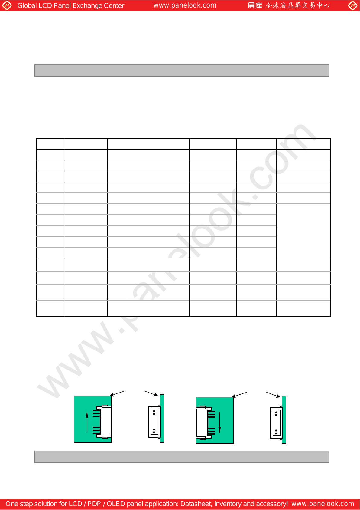
◆◆◆◆ Rear view of LCM
14
…
PCB
…
1
PCB
…
…
1
<Master>
Ver1.0
12
<Slave>
9 / 35
Global LCD Panel Exchange Center
www.panelook.com
One step solution for LCD / PDP / OLED panel application: Datasheet, inventory and accessory!
www.panelook.com
3-3. Signal Timing Specifications
Table 6 shows the signal timing required at the input of the LVDS transmitter. All of the interface signal
timings should be satisfied with the following specification for normal operation.
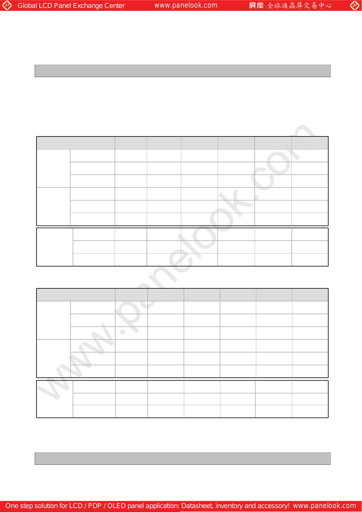
Table 6-1. TIMING TABLE for NTSC (DE Only Mode)
ITEM Symbol Min Typ Max Unit Note
Display Period tHV - 960 - tclk
LD420WUB
Product Specification
Horizontal
Vertical
Frequency
Blank tHB 100 140 240 tclk
Total tHP 1060 1100 1200 tclk 2200/2
Display Period tVV - 1080 - tHP
Blank tVB 11 45 69 tHP
Total tVP 1091 1125 1149 tHP
DCLK fCLK 70 74.25 77 MHz 148.5/2
Horizontal fH 65 67.5 70 KHz
Vertical fV 57 60 63 Hz
Table 6-2. TIMING TABLE for PAL (DE Only Mode)
ITEM Symbol Min Typ Max Unit Note
Display Period tHV - 960 - tclk
Horizontal
Blank tHB 100 140 240 tclk
Total tHP 1060 1100 1200 tclk 2200/2
Display Period tVV - 1080 - tHP
Vertical
Frequency
Note
The Input of HSYNC & VSYNC signal does not have an effect on normal operation(DE Only Mode).
Blank tVB 228 270 300 tHP
Total tVP 1308 1350 1380 tHP
DCLK fCLK 70 74.25 77 MHz 148.5/2
Horizontal fH 65 67.5 70 KHz
Vertical fV 47 50 53 Hz
The performance of the electro-optical characteristics may be influenced by variance of the vertical
refresh rate.
Ver1.0
10 / 35
Global LCD Panel Exchange Center
www.panelook.com
One step solution for LCD / PDP / OLED panel application: Datasheet, inventory and accessory!
www.panelook.com
3-4. LVDS Signal Specification
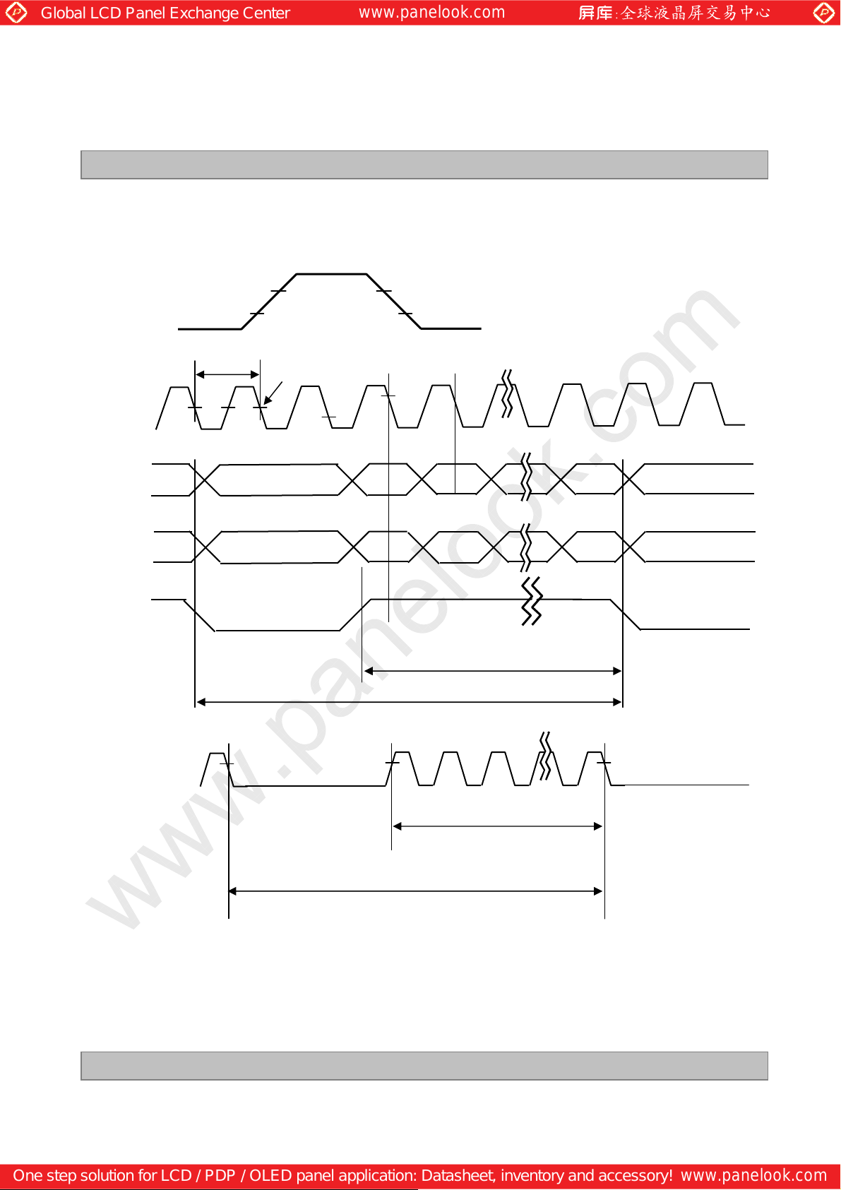
3-4-1. LVDS Input Signal Timing Diagram
LD420WUB
Product Specification
DE, Data
DCLK
First data
Second data
0.7VDD
0.3VDD
tCLK
DE(Data Enable)
0.5 VDD
Invalid data
Invalid data
Valid data
Pixel 0,0
Valid data
Pixel 1,0
tHP
Pixel 2,0
Pixel 3,0
Invalid data
Invalid data
tHV
DE(Data Enable)
Ver1.0
1 1080
tVV
tVP
11 / 35
 Loading...