

LG Display LD420EUP-SEA2 Specification
Global LCD Panel Exchange Center
)
(
(
Preliminary Specification
)
Final Specification
www.panelook.com
LD420EUP
Product Specification
SPECIFICATION
FOR
APPROVAL
Title 42.0” WUXGA TFT LCD
BUYER General
MODEL
APPROVED BY
/
/
SIGNATURE
DATE
SUPPLIER LG DISPLAY Co., Ltd.
*MODEL LD420EUP
SUFFIX SEA2
APPROVED BY
K. S. Nah
/ Chief Senior Engineer
REVIEWED BY
M.J. Lee
/ Chief Senior Engineer
SIGNATURE
DATE
PREPARED BY
J.H. Song
/
Please return 1 copy for your confirmation with
your signature and comments.
Ver. 1.0 1 / 40
One step solution for LCD / PDP / OLED panel application: Datasheet, inventory and accessory!
/ Senior Engineer
PD Product Design Dept.
LG Display Co., Ltd
www.panelook.com
Global LCD Panel Exchange Center
www.panelook.com
LD420EUP
Product Specification
CONTENTS
Number ITEM
COVER
CONTENTS
RECORD OF REVISIONS
1 GENERAL DESCRIPTION
2 ABSOLUTE MAXIMUM RATINGS
3 ELECTRICAL SPECIFICATIONS
3-1 ELECTRICAL CHARACTERISTICS
3-2 INTERFACE CONNECTIONS
3-3 SIGNAL TIMING SPECIFICATIONS
3-4 LVDS SIGNAL SPECIFICATIONS
3-5 COLOR DATA REFERENCE
3-6 POWER SEQUENCE
4 OPTICAL SPECIFICATIONS
5 MECHANICAL CHARACTERISTICS
Page
1
2
3
4
5
6
6
8
11
12
15
16
18
22
6 RELIABILITY
7 INTERNATIONAL STANDARDS
7-1 SAFETY
7-2 EMC
7-3 ENVIRONMENT
8 PACKING
8-1 INFORMATION OF LCM LABEL
8-2 PACKING FORM
9 PRECAUTIONS
9-1 MOUNTING PRECAUTIONS
9-2 OPERATING PRECAUTIONS
9-3 ELECTROSTATIC DISCHARGE CONTROL
9-4 PRECAUTIONS FOR STRONG LIGHT EXPOSURE
9-5 STORAGE
9-6 HANDLING PRECAUTIONS FOR PROTECTION FILM
25
26
26
26
26
27
27
27
28
28
28
29
29
29
29
9-7 APPROPRIATE CONDITION FOR PUBLIC DISPLAY
Ver. 1.0 2 / 40
One step solution for LCD / PDP / OLED panel application: Datasheet, inventory and accessory!
29
www.panelook.com
Global LCD Panel Exchange Center
www.panelook.com
Product Specification
RECORD OF REVISIONS
Revision No. Revision Date Page Description
1.0 Aug.14.2012 - Final Specification
LD420EUP
Ver. 1.0 3 / 40
One step solution for LCD / PDP / OLED panel application: Datasheet, inventory and accessory!
www.panelook.com
Global LCD Panel Exchange Center
XUGnGk
www.panelook.com
LD420EUP
Product Specification
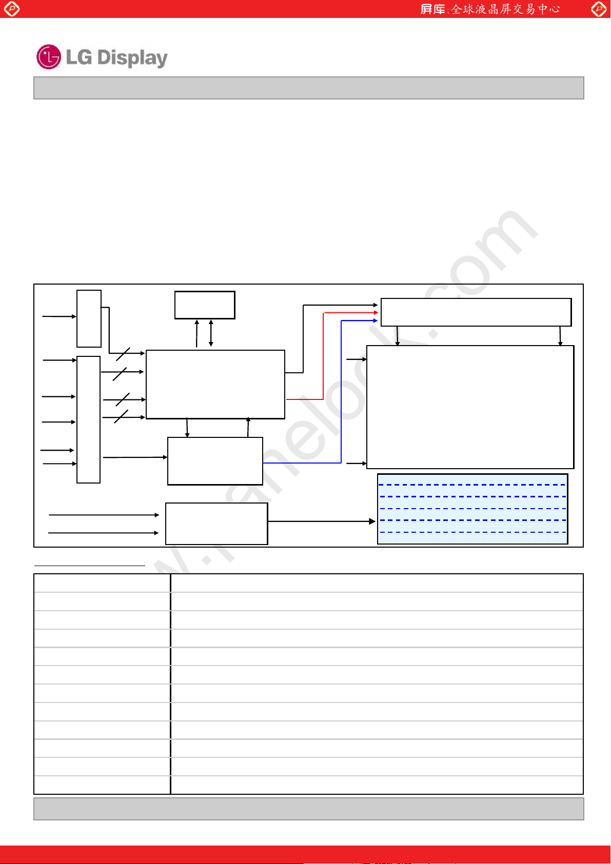
The LD420EUP is a Color Active Matrix Liquid Crystal Display with an integral Light Emitting Diode (LED)
backlight system. The matrix employs a-Si Thin Film Transistor as the active element.
It is a transmissive display type which is operating in the normally black mode. It has a 42.02 inch diagonally
measured active display area with WUXGA resolution (1080 vertical by 1920 horizontal pixel array).
Each pixel is divided into Red, Green and Blue sub-pixels or dots which are arrayed in vertical stripes.
Gray scale or the luminance of the sub-pixel color is determined with a 10-bit gray scale signal for each dot.
Therefore, it can present a palette of more than 1.06Bilion colors. It has been designed to apply the 10-bit 4-port
LVDS interface. It is intended to support Public Display where high brightness, super wide viewing angle, high
color gamut, high color depth and fast response time are important.
EPI (RGB)
LVDS
CN2
(41pin)
EEPROM
2Port
SDA
Integrated
Control
Signals
Power Signals
LVDS
2Port
LVDS
Select
L-DIM
Enable
Bit
Select
+12.0V
CN1
(51pin)
LVDS 3,4
LVDS 1,2
Option
signal
I2C
SCL
Timing Controller
LVDS Rx + L/D + DGA + ODC
Power Circuit
Block
SIN, SCLK, V_Sync
+24.0V, GND, On/Off
ExtV
BR-B
LED Driver
General Features
Active Screen Size 42.02 inches(1067.31mm) diagonal
G1
G1080
Source Driver Circuit
S1 S1920
TFT - LCD Panel
(1920 Ý RGB Ý 1080 pixels)
1B
L-Dimming : 12 Block
6B
7B
12B
Outline Dimension
958.4(H) Ý 551.3(V) X 10.8(B)/24.0 mm(D) (Typ.)
Pixel Pitch 0.4845 mm x 0.4845 mm
Pixel Format 1920 horiz. by 1080 vert. Pixels, RGB stripe arrangement
Color Depth 10bit(D), 1.06Billon colors
2
Luminance, White 700 cd/m
(Center 1point ,Typ.)
Viewing Angle (CR>10) Viewing angle free ( R/L 178 (Min.), U/D 178 (Min.))
Power Consumption Total 91.5W(Typ.) [Logic= 8.3W, LED Driver=83.2W(ExtVbr_B=100% )]
Weight 9.2 Kg (Typ.)
Display Mode Transmissive mode, Normally black
Surface Treatment Hard coating(3H), Anti-glare treatment of the front polarizer (Haze 10%)
Possible Display Type Landscape and Portrait Enabled
Ver. 1.0 4 / 40
One step solution for LCD / PDP / OLED panel application: Datasheet, inventory and accessory!
www.panelook.com
Global LCD Panel Exchange Center
www.panelook.com
LD420EUP
Product Specification
2. Absolute Maximum Ratings
The following items are maximum values which, if exceeded, may cause faulty operation or permanent damage
to the LCD module.
Table 1. ABSOLUTE MAXIMUM RATINGS
Parameter Symbol
Unit Note
Min Max
Value
LCD Circuit V
LCD -0.3 +14.0 VDC
Power Input Voltage
Driver V
ON/OFF V
BL -0.3 + 27.0 VDC
OFF / VON -0.3 +5.5 VDC
Driver Control Voltage
Brightness EXTVBR-B 0.0 +5.5 VDC
T-Con Option Selection Voltage VLOGIC -0.3 +4.0 VDC
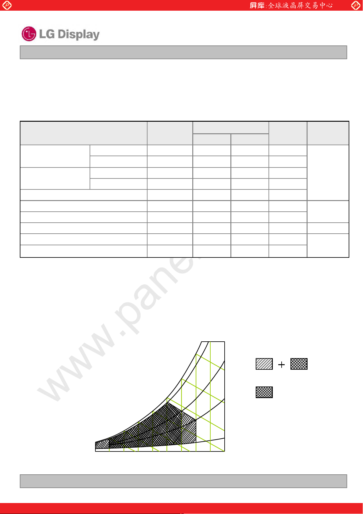
Operating Temperature TOP 0+50
Storage Temperature T
Panel Front Temperature T
Operating Ambient Humidity H
Storage Humidity H
Note
1. Ambient temperature condition (Ta = 25 r 2 ¶C )
ST -20 +60
SUR -+68
OP 10 90 %RH
ST 10 90 %RH
¶C
¶C
¶C
2. Temperature and relative humidity range are shown in the figure below.
Wet bulb temperature should be Max 39¶C, and no condensation of water.
3. Gravity mura can be guaranteed below 50¶C condition.
4. The maximum operating temperatures is based on the test condition that the surface temperature
of display area is less than or equal to 68¶C with LCD module alone in a temperature controlled chamber.
Thermal management should be considered in final product design to prevent the surface temperature of
display area from being over 68. The range of operating temperature may be degraded in case of
improper thermal management in final product design.
90%
1
2,3
4
2,3
60
60%
Wet Bulb
Temperature [
10
0
10 20 30 40 50 60 70 800-20
Dry Bulb Temperature [
20
50
¶C]
40
40%
30
Humidity [(%)RH]
10%
¶C]
Storage
Operation
Ver. 1.0 5 / 40
One step solution for LCD / PDP / OLED panel application: Datasheet, inventory and accessory!
www.panelook.com
Global LCD Panel Exchange Center
www.panelook.com
LD420EUP
Product Specification
3. Electrical Specifications
3-1. Electrical Characteristics
It requires two power inputs. One is employed to power for the LCD circuit. The other Is used for the LED
backlight and LED Driver circuit.
Table 2. ELECTRICAL CHARACTERISTICS
Value
Parameter Symbol
Min Typ Max
Circuit :
Unit Note
Power Input Voltage V
Power Input Current ILCD
Power Consumption P
Rush current I
LCD 10.8 12.0 13.2 VDC
- 690 900 mA 1
- 975 1,265 mA 2
LCD 8.3 10.8 Watt 1
RUSH --3.0A 3
Note
1. The specified current and power consumption are under the V
=12.0V, Ta=25 r 2¶C, fV=120Hz condition,
LCD
and mosaic pattern(8 x 6) is displayed and fV is the frame frequency.
2. The current is specified at the maximum current pattern.
3. The duration of rush current is about 2ms and rising time of power input is 0.5ms (min.).
4. Ripple voltage level is recommended under ᇹ5% of typical voltage
White : 1023 Gray
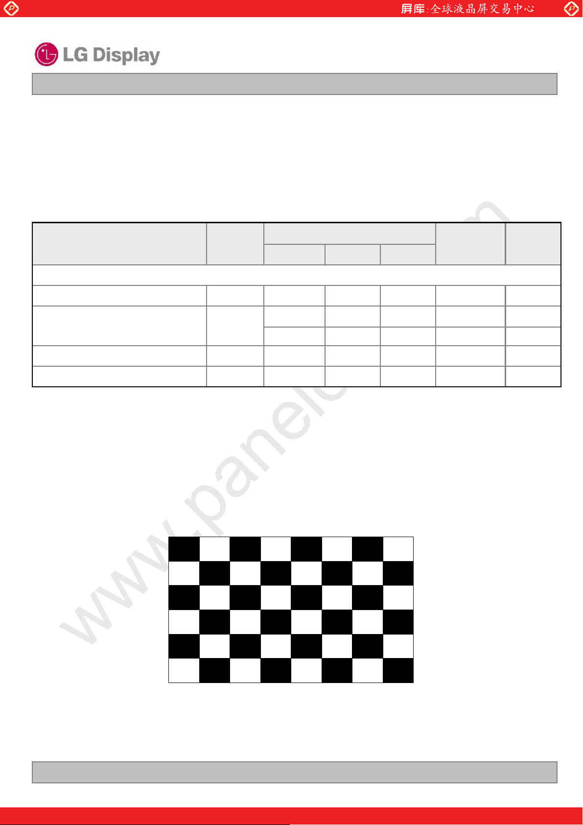
Black : 0 Gray
Mosaic Pattern(8 x 6)
Ver. 1.0 6 / 40
One step solution for LCD / PDP / OLED panel application: Datasheet, inventory and accessory!
www.panelook.com
Global LCD Panel Exchange Center
www.panelook.com
Product Specification
Table 3. ELECTRICAL CHARACTERISTICS (Continue)
LD420EUP
Parameter Symbol
LED Driver :
Power Supply Input Voltage VBL 22.8 24.0 25.2 Vdc 1
Power Supply Input Current IBL
Power Supply Input Current (In-Rush) In-rush - - 5.0 A
Power Consumption PBL -
On/Off
Input Voltage for
Control System
Signals
Life Time 50,000 60,000 Hrs 2
Brightness Adjust Ext V
PWM Frequency for
NTSC & PAL
Pulse Duty Level
(PWM)
On V on 2.5 - 5.0 Vdc
Off V off -0.3 0.0 0.7 Vdc
BR-B
PAL 100 Hz 3
NTSC 120 Hz 3
High Level 2.4 - 5.0
Low Level 0.0 - 0.7
Min Typ Max
-
1 - 100 %
Values
3.46 3.73 A 1
83.2 89.5
Unit Notes
VBL = 22.8V
Ext V
BR-B
W1
On Duty
Vdc
Vdc
HIGH : on duty
LOW : off duty
= 100%
4
6
Notes :
1. Electrical characteristics are determined after the unit has been ‘ON’ and stable for approximately 60
minutes at 25·2¶C. The specified current and power consumption are under the typical supply Input voltage
24Vand V
BR (ExtVBR-B : 100%), it is total power consumption.
2. The life time is determined as the time which luminance of the LED is 50% compared to that of initial
value at the typical LED current (ExtVBR-B :100%) on condition of continuous operating in LCM state at
25·2¶C. (Min @ L50B10)
3. LGD recommend that the PWM freq. is synchronized with One time harmonic of V_sync signal of system.
Though PWM frequency is over 120Hz (max 252Hz), function of LED Driver is not affected.
4. The duration of rush current is about 200ms. This duration is applied to LED on time.
5. Even though inrush current is over the specified value, there is no problem if I
2
T spec of fuse is satisfied.
6. Ext_PWM Signal have to input available duty range.
Between 99% and 100%
ExtVBR-B 0% and 100% are available.
But
High
ExtVBR-B duty have to be avoided. ( 99% < ExtVBR-B < 100%)
Available duty range
Low
0%
1%
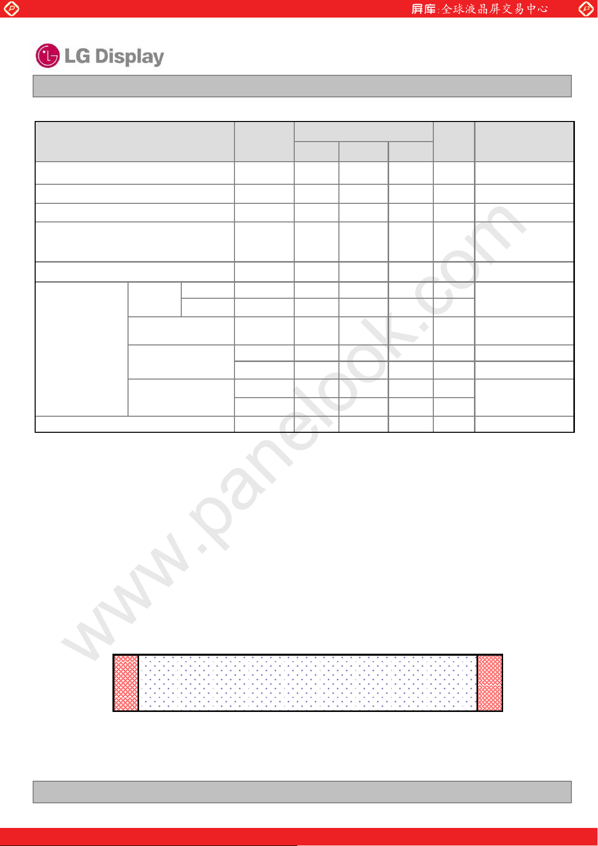
99% 100%Ext_PWM Input Duty
Ver. 1.0 7 / 40
One step solution for LCD / PDP / OLED panel application: Datasheet, inventory and accessory!
www.panelook.com
Global LCD Panel Exchange Center
www.panelook.com
LD420EUP
Product Specification
3-2. Interface Connections
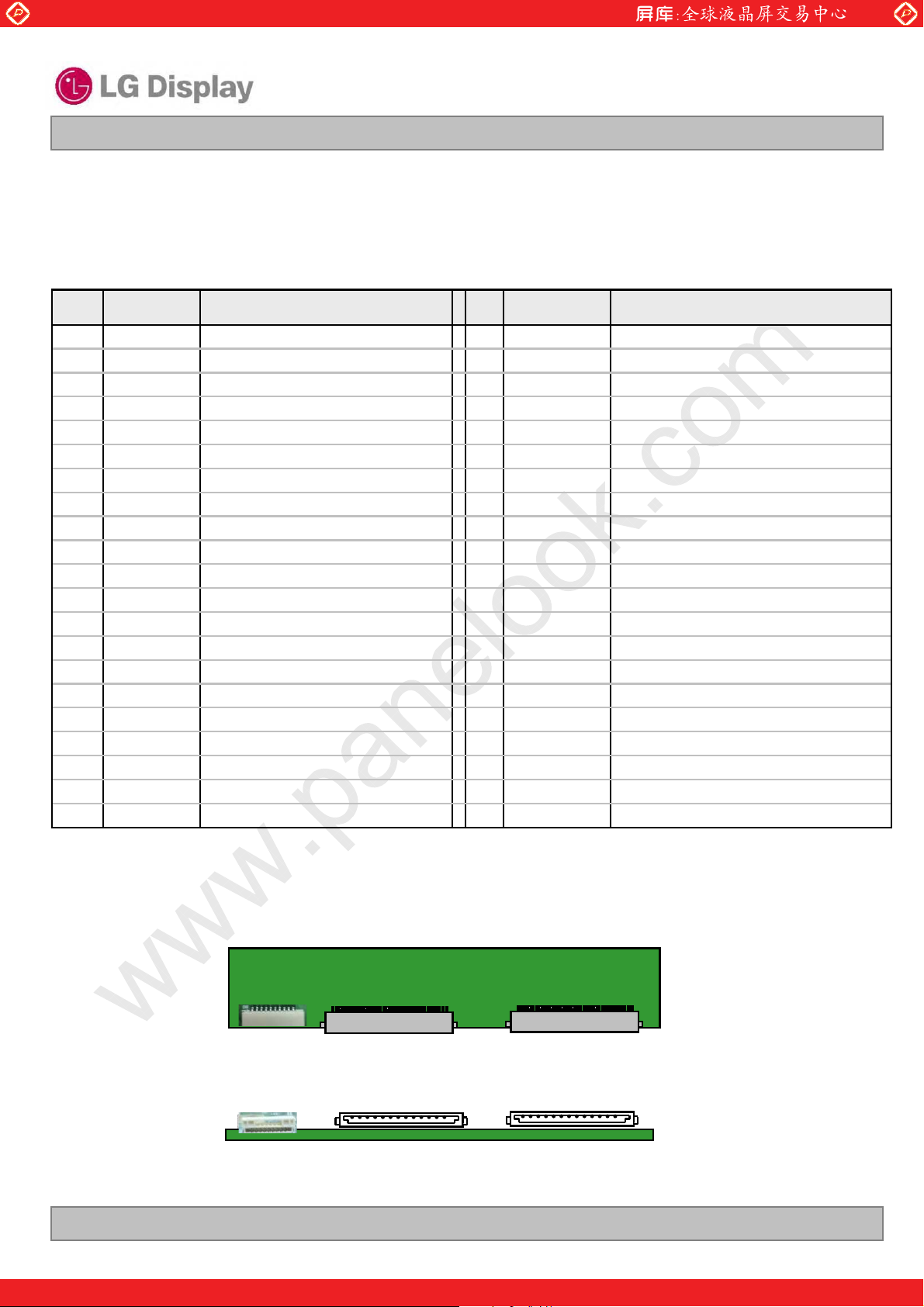
This LCD module employs two kinds of interface connection, 51-pin connector and 41-pin connector are used
for the module electronics and 14-pin connector is used for the integral backlight system.
3-2-1. LCD Module
- LCD Connector(CN1): FI-RE51S-HF(manufactured by JAE) or compatible
- Mating Connector : FI-R51HL(JAE) or compatible
Table 4-1. MODULE CONNECTOR(CN1) PIN CONFIGURATION
No Symbol Description No Symbol Description
1NC
2
3
4
5
6
7
8
9
10
11 GND
12 R1AN
13 R1AP
14 R1BN
15
16 R1CN
17 R1CP
18 GND
19 R1CLKN
20
21 GND
22 R1DN
23 R1DP
24 R1EN
25 R1EP
26
NC
NC
NC
NC
NC
LVDS Select
NC
NC
L-DIM Enable ಫHಬ Only, Note 5
R1BP
R1CLKP
NC or GND
Note 4
Note 4
Note 4
Note 4
Note 4
Note 4
ಫHಬ =JEIDA , ಫLಬ or NC = VESA
Note 4
Note 4
Ground
FIRST LVDS Receiver Signal (A-)
FIRST LVDS Receiver Signal (A+)
FIRST LVDS Receiver Signal (B-)
FIRST LVDS Receiver Signal (B+)
FIRST LVDS Receiver Signal (C-)
FIRST LVDS Receiver Signal (C+)
Ground
FIRST LVDS Receiver Clock Signal(-)
FIRST LVDS Receiver Clock Signal(+)
Ground
FIRST LVDS Receiver Signal (D-)
FIRST LVDS Receiver Signal (D+)
FIRST LVDS Receiver Signal (E-)
FIRST LVDS Receiver Signal (E+)
NC or Ground
27
28
29
30
31
32
33
34
35
36
37
38
39
40 R2EN
41 R2EP
42
43
44
45
46
47
48
49
50
51
Bit Select
R2AN
R2AP
R2BN
R2BP
R2CN
R2CP
GND
R2CLKN
R2CLKP
GND
R2DN
R2DP
NC or
GND
NC or GND
GND Ground
GND Ground
GND Ground
NC No connection
VLCD Power Supply +12.0V
VLCD Power Supply +12.0V
VLCD Power Supply +12.0V
VLCD Power Supply +12.0V
-- -
ೢHೣ or NC= 10bit(D) , ೢLೣ = 8bit
SECOND LVDS Receiver Signal (A-)
SECOND LVDS Receiver Signal (A+)
SECOND LVDS Receiver Signal (B-)
SECOND LVDS Receiver Signal (B+)
SECOND LVDS Receiver Signal (C-)
SECOND LVDS Receiver Signal (C+)
Ground
SECOND LVDS Receiver Clock Signal(-)
SECOND LVDS Receiver Clock Signal(+)
Ground
SECOND LVDS Receiver Signal (D-)
SECOND LVDS Receiver Signal (D+)
SECOND LVDS Receiver Signal (E-)
SECOND LVDS Receiver Signal (E+)
No Connection or Ground
No Connection or Ground
Note:
1. All GND (ground) pins should be connected together to the LCD module’s metal frame.
2. All V
LCD (power input) pins should be connected together.
3. All input levels of LVDS signals are based on the EIA 644 Standard.
4. These pins are reserved only for LGD (Do not connect)
5. All evaluation was verified based on L-DIM “H” and should keep “H” status during the operation.
Ver. 1.0 8 / 40
One step solution for LCD / PDP / OLED panel application: Datasheet, inventory and accessory!
www.panelook.com
Global LCD Panel Exchange Center
www.panelook.com
Product Specification
-LCD Connector (CN2) : FI-RE41S-HF (manufactured by JAE) or compatible
- Mating Connector : FI-RE41HL
Table 4-2. MODULE CONNECTOR(CN2) PIN CONFIGURATION
No Symbol Description No Symbol Description
LD420EUP
1
2
3
4NC
5
6
7
8
9
10
11
12
13 RB3P
14
15
16
17
18 RCLK3P
19
20
21
NC
NC
NC
NC
NC
NC
NC
GND
RA3N
RA3P
RB3N
RC3N
RC3P
GND
RCLK3N
GND
RD3N
RD3P
No connection 22
No connection 23
No connection 24 GND Ground
No connection
No connection
No connection 27
No connection 28
No connection 29 RB4P
Ground
THIRD LVDS Receiver Signal (A-)
THIRD LVDS Receiver Signal (A+)
THIRD LVDS Receiver Signal (B-)
THIRD LVDS Receiver Signal (B+)
THIRD LVDS Receiver Signal (C-)
THIRD LVDS Receiver Signal (C+)
Ground
THIRD LVDS Receiver Clock Signal(-)
THIRD LVDS Receiver Clock Signal(+)
Ground
THIRD LVDS Receiver Signal (D-)
THIR
D LVDS Receiver Signal (D+)
25 GND Ground
26
30
31
32
33
34 RCLK4P
35
36
37
38
39
40 GND Ground
41 GND Ground
-
RE3N
RE3P
RA4N
RA4P
RB4N
RC4N
RC4P
GND
RCLK4N
GND
RD4N
RD4P
RE4N
RE4P
THIRD LVDS Receiver Signal (E-)
THIRD LVDS Receiver Signal (E+)
FORTH LVDS Receiver Signal (A-)
FORTH LVDS Receiver Signal (A+)
FORTH LVDS Receiver Signal (B-)
FORTH LVDS Receiver Signal (B+)
FORTH LVDS Receiver Signal (C-)
FORTH LVDS Receiver Signal (C+)
Ground
FORTH LVDS Receiver Clock Signal(-)
FORTH LVDS Receiver Clock Signal(+)
Ground
FORTH LVDS Receiver Signal (D-)
FORTH LVDS Receiver Signal (D+)
FORTH LVDS Receiver Signal (E-)
FORTH LVDS Receiver Signal (E+)
Note :
1. All GND (ground) pins should be connected together to the LCD module’s metal frame.
2. LVDS pin (pin No. #22,23,38,39) are used for 10Bit(D) of the LCD module.
If used for 8Bit(R), these pins are no connection.
CN3
#1 #10
CN3
#1 #10
CN1 CN2
#1 #51 #1 #41
#1 #51
CN1 CN2
#1 #41
Rear view of LCM
Ver. 1.0 9 / 40
One step solution for LCD / PDP / OLED panel application: Datasheet, inventory and accessory!
www.panelook.com
Global LCD Panel Exchange Center
www.panelook.com
Product Specification
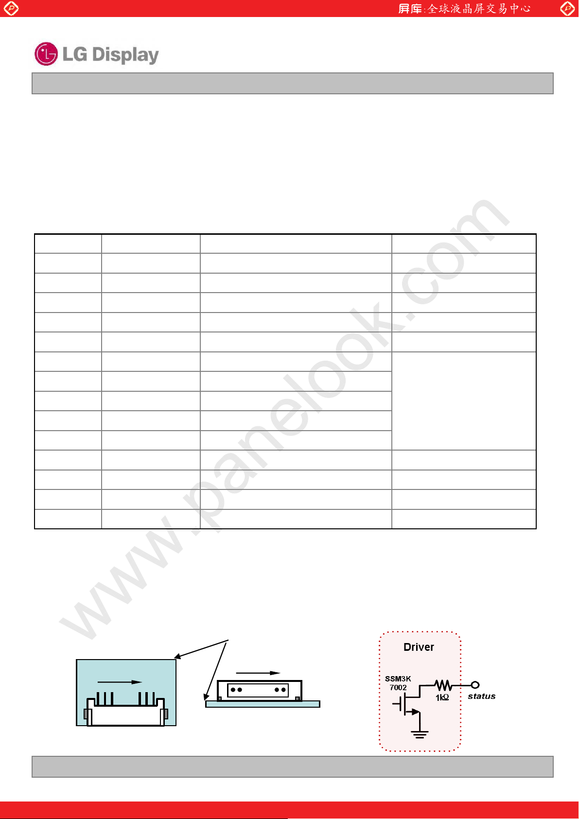
3-2-2. Backlight Module
Master
-LED Driver Connector
: 20022WR - H14B2(Yeonho)
Mating Connector
: 20022HS - 14B2(Yeonho)
Table 5. LED DRIVER CONNECTOR PIN CONFIGURATION
Pin No Symbol Description Note
LD420EUP
1
2
3
4
5
6
7
8
9
10
11
12
13
14
V
BL
V
BL
V
BL
V
BL
V
BL
GND
GND
GND
GND
GND
Status
VON/OFF
NC Don’t care
EXT V
BR-B
Power Supply +24.0V
Power Supply +24.0V
Power Supply +24.0V
Power Supply +24.0V
Power Supply +24.0V
Backlight Ground
Backlight Ground
Backlight Ground
Backlight Ground
Backlight Ground
Back Light Status 2
Backlight ON/OFF control
External PWM 3
Notes :1. GND should be connected to the LCD module’s metal frame.
2. Normal : Low (under 0.7V) / Abnormal : Open
3. High : on duty / Low : off duty, Pin#14 can be opened. ( if Pin #14 is open , EXT V
4. Each impedance of pin #12 and 14 is over 50 [KΩ].
1
is 100% )
BR-B
ଝ
ଝ Rear view of LCM
Status
PCB
1
14
…
1
14
…
<Master>
Ver. 1.0 10 / 40
One step solution for LCD / PDP / OLED panel application: Datasheet, inventory and accessory!
www.panelook.com
Global LCD Panel Exchange Center
www.panelook.com
Product Specification
3-3. Signal Timing Specifications
Table 6 shows the signal timing required at the input of the LVDS transmitter. All of the interface signal
timings should be satisfied with the following specification for normal operation.
Table 6. TIMING TABLE (DE Only Mode)
ITEM Symbol Min Typ Max Unit Note
LD420EUP
Horizontal
Vertical
Frequency
Display
Period
Blank t
Total t
Display
Period
Blank t
Total t
ITEM Symbol Min Typ Max Unit Note
DCLK f
Horizontal fH 121.8 135 140 KHz 2
Vertical f
HV 480 480 480 tCLK 1920 / 4
t
HB 40 70 200 tCLK 1
HP 520 550 680 tCLK
VV 1080 1080 1080 Lines
t
VB
VP
CLK 66.97 74.25 78.00 MHz
V
20
(228)
1100
(1308)
108
(95)
45
(270)
1125
(1350)
120
(100)
86
(300)
1166
(1380)
122
(104)
Lines 1
Lines
Hz
NTSC
(PAL)
2
Note:
1. The input of HSYNC & VSYNC signal does not have an effect on normal operation (DE Only Mode).
If you use spread spectrum of EMI, add some additional clock to minimum value for clock margin.
2. The performance of the electro-optical characteristics may be influenced by variance of the vertical
refresh rate and the horizontal frequency
Timing should be set based on clock frequency.
Ver. 1.0 11 / 40
One step solution for LCD / PDP / OLED panel application: Datasheet, inventory and accessory!
www.panelook.com
Global LCD Panel Exchange Center
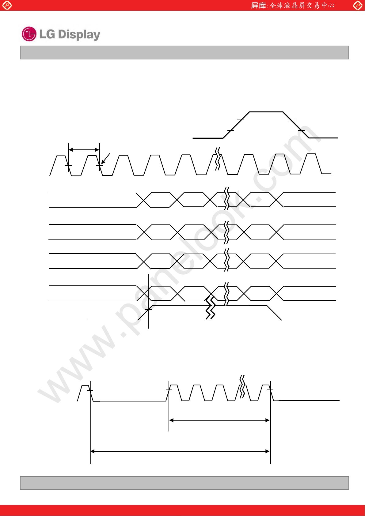
3-4. LVDS Signal Specification
3-4-1. LVDS Input Signal Timing Diagram
www.panelook.com
LD420EUP
Product Specification
DCLK
First data
Second data
Third data
Forth data
tCLK
0.5 VDD
Invalid data
Invalid data
Invalid data
Invalid data
DE, Data
Valid data
Pixel 0
Valid data
Pixel 1
Valid data
Pixel 2
Valid data
Pixel 3
Pixel 4
Pixel 5
Pixel 6
Pixel 7
0.7VDD
0.3VDD
Invalid data
Invalid data
Invalid data
Invalid data
DE(Data Enable)
* tHB = tHFP + tWH +tHBP
* tVB = tVFP + tWV +tVBP
1 1080
DE(Data Enable)
tVV
tVP
Ver. 1.0 12 / 40
One step solution for LCD / PDP / OLED panel application: Datasheet, inventory and accessory!
www.panelook.com
 Loading...