

Page 1
Global LCD Panel Exchange Center
www.panelook.com
One step solution for LCD / PDP / OLED panel application: Datasheet, inventory and accessory!
www.panelook.com
LC550MUT
Liquid Crystal Display
Product Specification
SPECIFICATION
FOR
APPROVAL
)
(
Preliminary Specification
)
(
Final Specification
SET MODEL
APPROVED BY
/
/
55.0” WUXGA TFT LCD Title
LGEBUYER
LC550MUT-SCA1LCD MODEL
*When you obtain standard approval,
please use the above model name without suffix
SIGNATURE
DATE
APPROVED BY
- /Team Leader
REVIEWED BY
- / Project Leader
LG Display Co., Ltd.SUPPLIER
LC550MUT*MODEL
SCA1SUFFIX
SIGNATURE
DATE
PREPARED BY
/
Please return 1 copy for your confirmation with
your signature and comments.
Ver. 0.3
- / Engineer
TV Product Development Dept.
LG Display Co., Ltd.
0 /29
Page 2
Global LCD Panel Exchange Center
www.panelook.com
One step solution for LCD / PDP / OLED panel application: Datasheet, inventory and accessory!
www.panelook.com
LC550MUT
Liquid Crystal Display
Product Specification
CONTENTS
CONTENTS
RECORD OF REVISIONS
GENERAL DESCRIPTION1
ABSOLUTE MAXIMUM RATINGS2
ELECTRICAL SPECIFICATIONS3
ELECTRICAL CHARACTERISTICS3-1
INTERFACE CONNECTIONS3-2
SIGNAL TIMING SPECIFICATIONS3-3
DATA MAPPING AND TIMING3-4
PANEL PIXEL STRUCTURE3-5
POWER SEQUENCE3-6
OPTICAL SPECIFICATIONS4
MECHANICAL CHARACTERISTICS5
ITEMNumber
Page
1COVER
2
3
4
5
6
6
11
14
17
18
19
20
24
Ver. 0.3
RELIABILITY6
INTERNATIONAL STANDARDS7
SAFETY7-1
ENVIRONMENT7-2
PACKING8
DESIGNATION OF LOT MARK8-1
PACKING FORM8-2
PRECAUTIONS9
MOUNTING PRECAUTIONS9-1
OPERATING PRECAUTIONS9-2
ELECTROSTATIC DISCHARGE CONTROL9-3
PRECAUTIONS FOR STRONG LIGHT EXPOSURE9-4
STORAGE9-5
HANDLING PRECAUTIONS FOR PROTECTION FILM9-6
26
27
27
27
28
28
28
29
29
29
30
30
30
30
1 /29
Page 3
Global LCD Panel Exchange Center
www.panelook.com
One step solution for LCD / PDP / OLED panel application: Datasheet, inventory and accessory!
www.panelook.com
LC550MUT
Liquid Crystal Display
Product Specification
RECORD OF REVISIONS
DescriptionPageRevision DateRevision No.
Preliminary Specification(First Draft) -Sep, 2, 20090.1
Power Consumption Updated3Dec, 4, 20090.2
Optical Specification Updated15
Power Consumption specification updated5May, 3, 20100.3
Data setup/hold time specification updated9
Power sequence specification updated14
Ver. 0.3
2 /29
Page 4
Global LCD Panel Exchange Center
www.panelook.com
One step solution for LCD / PDP / OLED panel application: Datasheet, inventory and accessory!
www.panelook.com
1. General Description
The LC550MUT is a Color Active Matrix Liquid Crystal Display with an integral Source PCB and the nine of
Gate Drive IC (GD-IC) at each side. The matrix employs a-Si Thin Film Transistor as the active element.
It is a transmissive display type which is operating in the normally black mode. It has a 54.64 inch diagonally
measured active display area with WUXGA resolution progressive mode (1080 vertical by 1920 horizontal
pixel array).
Each pixel is divided into Red, Green and Blue sub-pixels or dots which are arrayed in vertical stripes.
Gray scale or the luminance of the sub-pixel color is determined with a 8-bit gray scale signal for each dot.
Therefore, it can present a palette of more than 16.7M colors.
It is intended to support LCD TV, PCTV where high brightness, super wide viewing angle, high color gamut,
high color depth and fast response time are important.
LC550MUT
Liquid Crystal Display
Product Specification
Power (VCC, VDD, VGH, VGL)
Source Control Signal
Gate Control Signal
Gamma Reference Voltage
mini-LVDS (RGB) for Left drive
Power (VCC, VDD, VGH, VGL)
Source Control Signal
Gate Control Signal
Gamma Reference Voltage
mini-LVDS (RGB) for Right drive
General Features
Drive IC Data Interface
Source Driver Circuit
CN1
(80pin)
Gate Driver Circuit
S1 S1920
G1
TFT - LCD Panel
CN2
(80pin)
G1080
54.64 inches(1387.8mm) diagonalActive Screen Size
1220.8 (H) x 693.8 (V) x1.94 (D) (Typ.)Outline Dimension
0.630 mm x 0.630 mmPixel Pitch
1920 horiz. by 1080 vert. Pixels, RGB stripe arrangementPixel Format
8-bit, 16.7 M colors Color Depth
Source D-IC : 8-bit mini-LVDS, and control signals TTL
Gate D-IC : Line on Glass (LOG) Through Source D-IC
Viewing angle free ( R/L 178 (Min.), U/D 178 (Min.))Viewing Angle (CR>10)
14.04[W] with LGE T-conPower Consumption
3.4kg(Typ)Weight
Transmissive mode, Normally blackDisplay Mode
Hard coating(3H), Anti-glare treatment of front polarizerSurface Treatment
(1920 × RGB × 1080 pixels)
Ver. 0.3
3 /29
Page 5
Global LCD Panel Exchange Center
www.panelook.com
One step solution for LCD / PDP / OLED panel application: Datasheet, inventory and accessory!
www.panelook.com
Liquid Crystal Display
Product Specification
2. Absolute Maximum Ratings
The following items are maximum values which, if exceeded, may cause faulty operation or damage to the
LCD module.
Table 1. ABSOLUTE MAXIMUM RATINGS
LC550MUT
Parameter Symbol
Source D-IC Analog Voltage VDD -0.3 +18.0 VDC
Gamma Ref. Voltage (Upper) VGMH ½VDD-0.5 VDD+0.5 VDC
Gamma Ref. Voltage (Low) VGML -0.3 ½ VDD+0.5 VDC
Operating Temperature TOP 0 +50 °C
Storage Temperature TST -20 +60 °C
Operating Ambient Humidity HOP 10 90 %RH
Storage Humidity HST 10 90 %RH
1. Ambient temperature condition (Ta = 25 ± 2 °C )
Note:
Value
Unit Note
Min Max
VDC+4.0-0.5VCCLogic Power Voltage
VDC+30.0 +18.0VGHGate High Voltage
VDC-4.0-8.0VGLGate Low Voltage
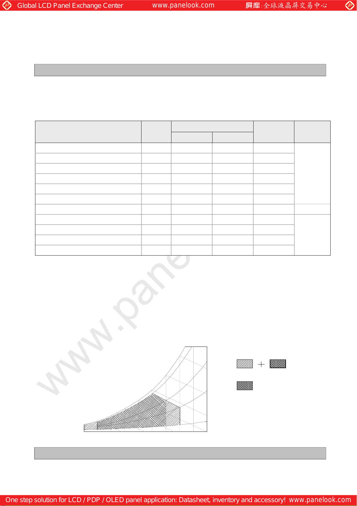
2. Temperature and relative humidity range are shown in the figure below. Wet bulb temperature
should be Max 39 °C and no condensation of water.
3. Gravity mura can be guaranteed below 40℃ condition.
4. The maximum operating temperature is based on the test condition that the surface temperature
of display area is less than or equal to 68 ℃ with LCD module alone in a temperature controlled
chamber. Thermal management should be considered in final product design to prevent the surface
temperature of display area from being over 68 ℃. The range of operating temperature may
degrade in case of improper thermal management in final product design.
90%
60
60%
1
4°C+68-TSURPanel Front Temperature
2,3
Ver. 0.3
Wet Bulb
Temperature [°C]
20
10
0
10 20 30 40 50 60 70 800-20
Dry Bulb Temperature [°C]
30
40
50
40%
10%
Humidity
[(%)RH]
Storage
Operation
4 /29
Page 6
Global LCD Panel Exchange Center
www.panelook.com
One step solution for LCD / PDP / OLED panel application: Datasheet, inventory and accessory!
www.panelook.com
3. Electrical Specifications
3-1. Electrical Characteristics
It requires several power inputs. The VCC is the basic power of LCD Driving power sequence, Which is used
to logic power voltage of Source D-IC and Gate D-IC.
Table 2. ELECTRICAL CHARACTERISTICS
Parameter Symbol Condition MIN TYP MAX Unit Note
Logic Power Voltage VCC - 3.0 3.3 3.6 VDC
Logic High Level Input Voltage VIH 2.7 VCC VDC
Logic Low Level Input Voltage VIL 0 0.6 VDC
Source D-IC Analog Voltage VDD - 15.8 16 16.2 VDC
Half Source D-IC Analog
Voltage
Gamma Reference Voltage
Common Voltage Vcom - 6.13 V
Mini-LVDS Clock frequency CLK 3.0V≤VCC ≤3.6V 312 MHz
mini-LVDS input Voltage
(Center)
mini-LVDS input Voltage
Distortion (Center)
mini-LVDS differential
Voltage range
mini-LVDS differential
Voltage range Dip
Gate High Voltage VGH 27.7 28.0 28.3 VDC
Gate Low Voltage VGL -5.5 -5.0 -5.1 VDC
Gate High Modulation Voltage VGHM 28 V
Total Power Current
Total Power Consumption
LC550MUT
Liquid Crystal Display
Product Specification
H_VDD - 7.9 8.0 8.1 VDC
V
GMH
V
GML
VIB
ΔVIB 0.8 V
VID 150 800 mV
ΔVID 25 800 mV
ILCD - 1170 mA 2
PLCD - 14.04 Watt 2
(GMA1 ~ GMA9) ½*VDD VDD-0.2
(GMA10 ~ GMA18) 0.2 ½*VDD
0.7 +
(VID/2)
Mini-LVDS Clock
and Data
(VCC-1.2)
− VID / 2
V
5
Note:
1. The specified current and power consumption are under the VLCD=12V., 25 ± 2°C, fV=120Hz
condition whereas mosaic pattern(8 x 6) is displayed and fVis the frame frequency.
2. The specified current and power consumption are measured with LGE T-con.
3 . All of the typical gate voltage should be controlled within 1% voltage level
4. Ripple voltage level is recommended under 10%
5. In case of mini-LVDS signal spec, refer to Fig 2 for the more detail.
6. Logic Level Input Signal : SOE,POL,GSP,H_CONV,OPT_N
7. HVDD Voltage level is half of VDD and it should be between Gamma9 and Gamma10
Ver. 0.3
5 /29
Page 7
Global LCD Panel Exchange Center
www.panelook.com
One step solution for LCD / PDP / OLED panel application: Datasheet, inventory and accessory!
www.panelook.com
VGH
VGHM
GND
VGL
LC550MUT
Liquid Crystal Display
Product Specification
Without GPM With GPM
VCM (0V)
FIG. 1 Gate Output Wave form without GPM and with GPM
VID
△VID
VID
* Differential Probe
△VIB
VIB
△VID
* Active Probe
FIG. 2 Description of VID, ΔVIB, ΔVID
* Source PCB
FIG. 3 Measure point
Ver. 0.3
6 /29
Page 8
Global LCD Panel Exchange Center
www.panelook.com
One step solution for LCD / PDP / OLED panel application: Datasheet, inventory and accessory!
www.panelook.com
Product Specification
3-2. Interface Connections
This LCD module employs two 80pin connector of interface connection, Each 80 pin connectors are used for
the module electronics.
3-2-1. LCD Module
- LCD Connector : TF06L-80S-0.5SH (Manufactured by HIROSE or Equivalent)
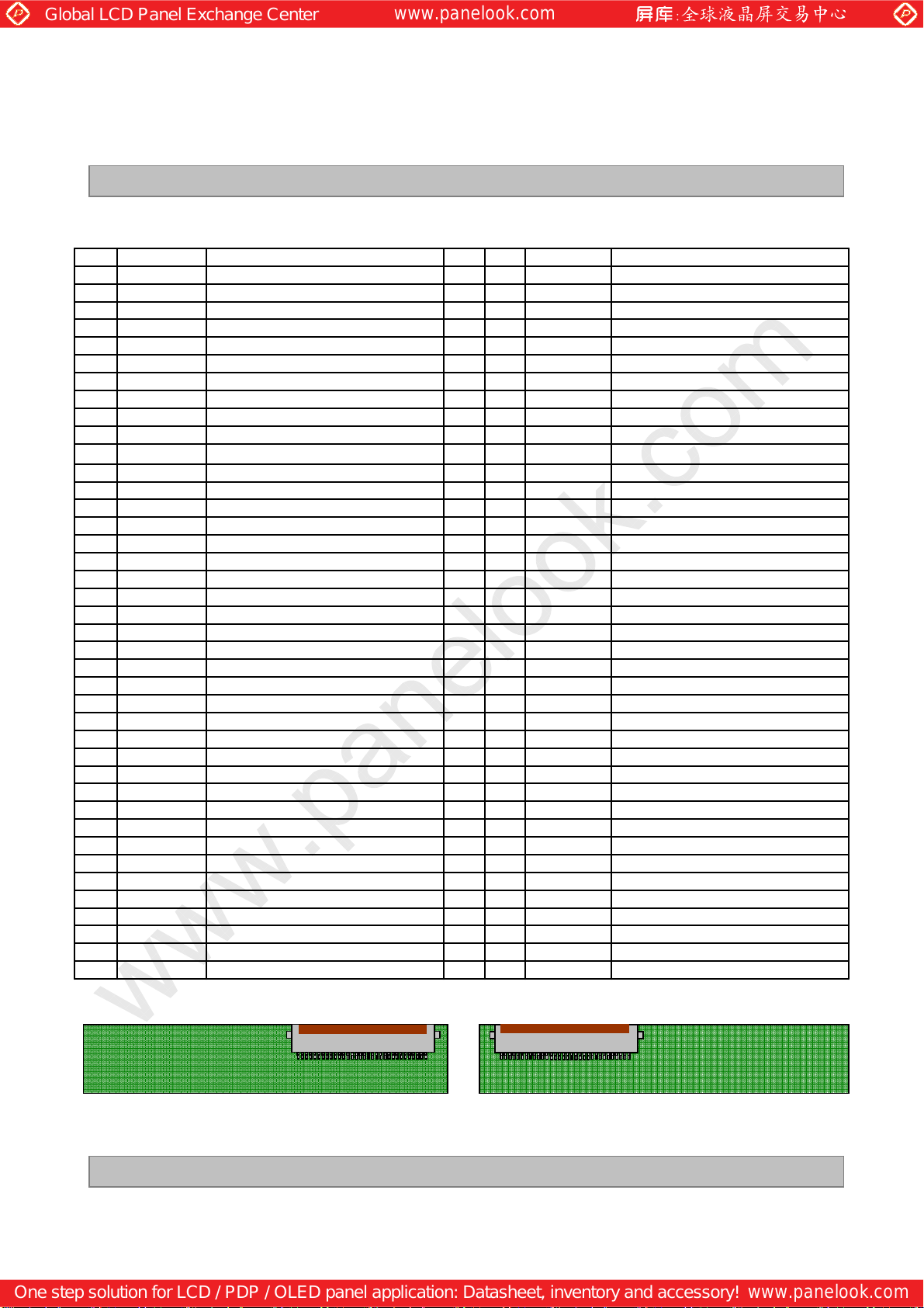
Table 4-1. Source PCB CONNECTOR(CN5) PIN CONFIGURATION
LRVCLK-27
GND28
LRV3 +29
LRV5 -34
GSP38
LC550MUT
Liquid Crystal Display
DescriptionSymbolNoDescriptionSymbolNo
SOE41GroundGND1
GND42Left Mini LVDS Receiver Signal(0+) LLV0 +2
GMA 143Left Mini LVDS Receiver Signal(0-) LLV0 -3
GMA 446Left Mini LVDS Receiver Signal(2+) LLV2 +6
GMA 648GroundGND8
GMA 1051GroundGND11
GMA 1353Left Mini LVDS Receiver Signal(3-) LLV3 -13
GMA 1656Left Mini LVDS Receiver Signal(5+) LLV5 +16
GMA 1858GroundGND18
GND65GroundGND25
SOURCE OUTPUT ENABLE
Ground
GAMMA VOLTAGE 1
N.CGMA 244Left Mini LVDS Receiver Signal(1+) LLV1 +4
GAMMA VOLTAGE 3GMA 345Left Mini LVDS Receiver Signal(1-) LLV1 -5
GAMMA VOLTAGE 4
GAMMA VOLTAGE 5GMA 547Left Mini LVDS Receiver Signal(2-) LLV2 -7
GAMMA VOLTAGE 6
N.CGMA 749Left Mini LVDS Receiver Clock(+)LLVCLK+9
GAMMA VOLTAGE 9GMA 950Left Mini LVDS Receiver Clock(-)LLVCLK-10
GAMMA VOLTAGE 10
N.CGMA 1252Left Mini LVDS Receiver Signal(3+) LLV3 +12
GAMMA VOLTAGE 13
GAMMA VOLTAGE 14GMA 1454Left Mini LVDS Receiver Signal(4+) LLV4 +14
GAMMA VOLTAGE 15GMA 1555Left Mini LVDS Receiver Signal(4-) LLV4 -15
GAMMA VOLTAGE 16
N.CGMA 1757Left Mini LVDS Receiver Signal(5-) LLV5 -17
GAMMA VOLTAGE 18
GroundGND59Left Mini LVDS Receiver Signal(0+) LRV0 +19
GroundGND60Left Mini LVDS Receiver Signal(0-) LRV0 -20
LTD OUTPUTZ_OUT61Left Mini LVDS Receiver Signal(1+) LRV1 +21
GroundGND62Left Mini LVDS Receiver Signal(1-) LRV1 -22
LEFT VCOM OUTPUTVCOML_OUT63Left Mini LVDS Receiver Signal(2+) LRV2 +23
LEFT VCOM FeedbackVCOML_FB64Left Mini LVDS Receiver Signal(2-) LRV2 -24
Ground
Gate High VoltageVGH66Left Mini LVDS Receiver Clock(+)LRVCLK+26
GroundGND67Left Mini LVDS Receiver Clock(-)
GATE SHIFT CLOCKGSC68Ground
GATE OUTPUT ENABLEGOE69Left Mini LVDS Receiver Signal(3+)
GroundGND70Left Mini LVDS Receiver Signal(3-) LRV3 -30
Gate Low VoltageVGL71Left Mini LVDS Receiver Signal(4+) LRV4 +31
GroundGND72Left Mini LVDS Receiver Signal(4-) LRV4 -32
DRIVER POWER SUPPLY VOLTAGEHVDD73Left Mini LVDS Receiver Signal(5+) LRV5 +33
DRIVER POWER SUPPLY VOLTAGEHVDD74Left Mini LVDS Receiver Signal(5-)
GroundGND75GroundGND35
LOGIC POWER SUPPLY VOLTAGEVCC76N.COPT_N36
LOGIC POWER SUPPLY VOLTAGEVCC77HORIZONTAL 2 DOT INVERSION SIGNALH_CONV37
GroundGND78GATE START PULSE
DRIVER POWER SUPPLY VOLTAGEVDD79POLARITY OUTPUT SIGNALPOL39
DRIVER POWER SUPPLY VOLTAGEVDD80GroundGND40
Notes : 1. More detail Information refer to application notes.
Ver. 0.3
7 /29
Page 9
Global LCD Panel Exchange Center
www.panelook.com
One step solution for LCD / PDP / OLED panel application: Datasheet, inventory and accessory!
www.panelook.com
Product Specification
Table 4-2. Source PCB CONNECTOR (CN6) PIN CONFIGURATION
LC550MUT
Liquid Crystal Display
DescriptionSymbolNoDescriptionSymbolNo
POL41DRIVER POWER SUPPLY VOLTAGEVDD1
GND42DRIVER POWER SUPPLY VOLTAGEVDD2
H_CONV44LOGIC POWER SUPPLY VOLTAGEVCC4
GND46GroundGND6
RLV0 -48DRIVER POWER SUPPLY VOLTAGEHVDD8
RLV2 +51Gate Low VoltageVGL11
RLVCLK+54GATE SHIFT CLOCKGSC14
GND56Gate High VoltageVGH16
RLV3 -58RIGHT VCOM OUTPUTVCOMR_FB18
RLV4 -60GroundGND20
GND63GAMMA VOLTAGE 1GMA 123
RRV0 +64N.CGMA 224
RRV0 -65GAMMA VOLTAGE 3GMA 325
RRV1 -67GAMMA VOLTAGE 5GMA 527
GND70GAMMA VOLTAGE 9GMA 930
RRV3 +74GAMMA VOLTAGE 14GMA 1434
RRV5 -79GroundGround39
POLARITY OUTPUT SIGNAL
Ground
SOURCE OUTPUT ENBLESOE43GroundGND3
HORIZONTAL 2 DOT INVERSION SIGNAL
N.COPT_N45LOGIC POWER SUPPLY VOLTAGEVCC5
Ground
Right Mini LVDS Receiver Signal(0+) RLV0 +47DRIVER POWER SUPPLY VOLTAGEHVDD7
Right Mini LVDS Receiver Signal(0-)
Right Mini LVDS Receiver Signal(1+) RLV1 +49GroundGND9
Right Mini LVDS Receiver Signal(1-) RLV1 -50N.COPT_P10
Right Mini LVDS Receiver Signal(2+)
Right Mini LVDS Receiver Signal(2-) RLV2 -52GroundGND12
GroundGND53GATE OUTPUT ENABLEGOE13
Right Mini LVDS Receiver Clock(+)
Right Mini LVDS Receiver Clock(-)RLVCLK-55GroundGND15
Ground
Right Mini LVDS Receiver Signal(3+) RLV3 +57GroundGND17
Right Mini LVDS Receiver Signal(3-)
Right Mini LVDS Receiver Signal(4+) RLV4 +59RIGHT VCOM FeedbackVCOMR_OUT19
Right Mini LVDS Receiver Signal(4-)
Right Mini LVDS Receiver Signal(5+) RLV5 +61LDT OUTPUTZ_OUT21
Right Mini LVDS Receiver Signal(5-) RLV5 -62GroundGND22
Ground
Right Mini LVDS Receiver Signal(0+)
Right Mini LVDS Receiver Signal(0-)
Right Mini LVDS Receiver Signal(1+) RRV1 +66GAMMA VOLTAGE 4GMA 426
Right Mini LVDS Receiver Signal(1-)
Right Mini LVDS Receiver Signal(2+) RRV2 +68GAMMA VOLTAGE 6GMA 628
Right Mini LVDS Receiver Signal(2-) RRV2 -69N.CGMA 729
Ground
Right Mini LVDS Receiver Clock(+)RRVCLK+71GAMMA VOLTAGE 10GMA 1031
Right Mini LVDS Receiver Clock(-)RRVCLK-72N.CGMA 1232
GroundGND73GAMMA VOLTAGE 13GMA 1333
Right Mini LVDS Receiver Signal(3+)
Right Mini LVDS Receiver Signal(3-) RRV3 -75GAMMA VOLTAGE 15GMA 1535
Right Mini LVDS Receiver Signal(4+) RRV4 +76GAMMA VOLTAGE 16GMA 1636
Right Mini LVDS Receiver Signal(4-) RRV4 -77N.CGMA 1737
Right Mini LVDS Receiver Signal(5+) RRV5 +78GAMMA VOLTAGE 18GMA 1838
Right Mini LVDS Receiver Signal(5-)
GroundGND80GATE START PULSEGSP40
Notes : 1. More detail Information refer to application notes.
#80
CN 6
#1
#80
CN 5
#1
Source Left PCBSource Right PCB
Ver. 0.3
8 /29
Page 10

Global LCD Panel Exchange Center
www.panelook.com
One step solution for LCD / PDP / OLED panel application: Datasheet, inventory and accessory!
www.panelook.com
3-3. Signal Timing Specifications
Table 6. Timing Requirements
Parameter Symbol Condition Min Typ Max Unit Note
LC550MUT
Liquid Crystal Display
Product Specification
Mini Clock pulse period
Mini Clock pulse low period
Mini Clock pulse high period
Mini Data setup time
Mini Data hold time
Reset low to SOE rising time
SOE to Reset input time
Receiver off to SOE timing
POL signal to SOE setup time
POL signal to SOE hold time
Reset High Period
SOE signal GSP setup time
SOE signal GSP Hold time
SOE signal Pulse Width
Note :
1. mini-LVDS timing measure conditions
: 268MHz < Clock Frequency < 312MHz, 150mV < VID < 800mV @ 3.0 < VCC < 3.3
2. Setup time and hold time should be satisfied at the same time
T1
T2
T3
T6
T7
T8
T9
T10
T11
T12
T13
T14
T15
T16
3.2 3.4 ns
1.6 - - ns
1.6 - - ns
0.55 - - ns
0.55 - - ns
0 - - ns
200 - - ns
10 - -
-5 - - ns
6 - - ns
3
100 ns
100 ns
200 ns
CLK
cycle
CLK
cycle
1
T1
70%
T7
T2
T5
70%
30%
T5
30%
30%
T4
30%
70%
VDIFF
T4
70%
VDIFF
CLK-
CLK+
LV0+, -
to
LV5+,-
T6 T7
50%
T3
T6
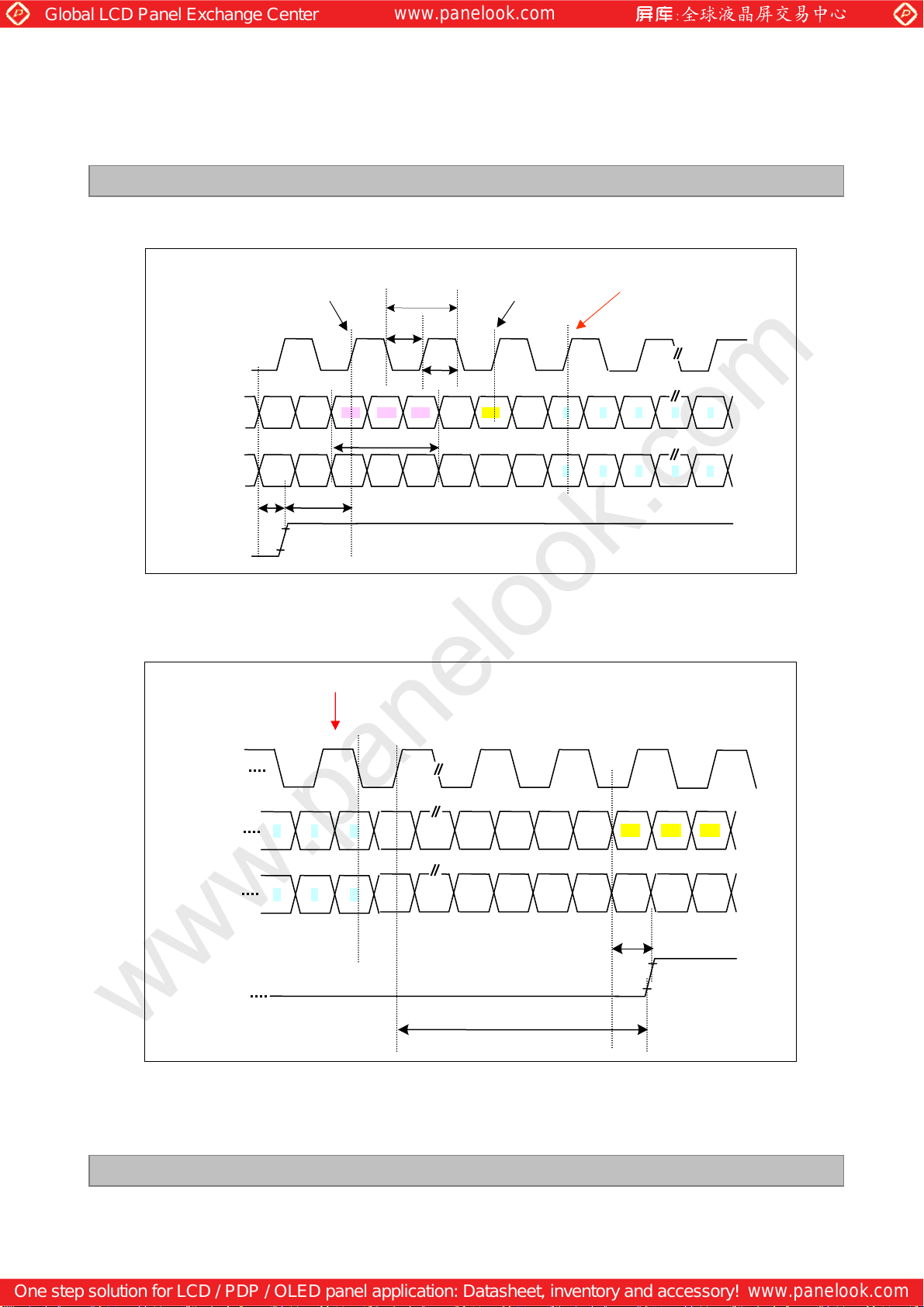
FIG 4. Source D-IC Input Data Latch Timing Waveform
Ver. 0.3
9 /29
Page 11
Global LCD Panel Exchange Center
www.panelook.com
One step solution for LCD / PDP / OLED panel application: Datasheet, inventory and accessory!
www.panelook.com
LC550MUT
Liquid Crystal Display
Product Specification
CLK+
LV0+,-
LV1+,-
to
LV5+,-
SOE
Read The Reset=H
NA
NA
T8
70%
30%
R=H R=H R=H NAR=L R=L NA D D DR=L DD
NA NA NA NANA NA NA D D DNA DD
T9
T13
Read The Reset=L 1stDATA
T1
T2
T3
FIG 5-1. Input Data Timing for 1stSource D-IC Chip
Last DATA
Ver. 0.3
CLK+
LV0+,-
LV1+,-
to
LV5+,-
SOE
(320)
D D D
D D D
(321)
NA NA NA NA NA R=LNA R=L R=L
NA NA NA NA NA NANA NA NA
T10
FIG 5-2. Last Data Latch to SOE Timing
T8
70%
30%
10 /29
Page 12

Global LCD Panel Exchange Center
www.panelook.com
One step solution for LCD / PDP / OLED panel application: Datasheet, inventory and accessory!
www.panelook.com
LC550MUT
Liquid Crystal Display
Product Specification
SOE
POL
GSP
GSP
70%
T16
T14
T11
70%
30%
30%
70%
T15
T12
70%
30%
70%
30%
70%
Ver. 0.3
SOE
1stline data 1stline output
FIG 6. POL, GSP and SOE Timing Waveform
11 /29
Page 13
Global LCD Panel Exchange Center
www.panelook.com
One step solution for LCD / PDP / OLED panel application: Datasheet, inventory and accessory!
www.panelook.com
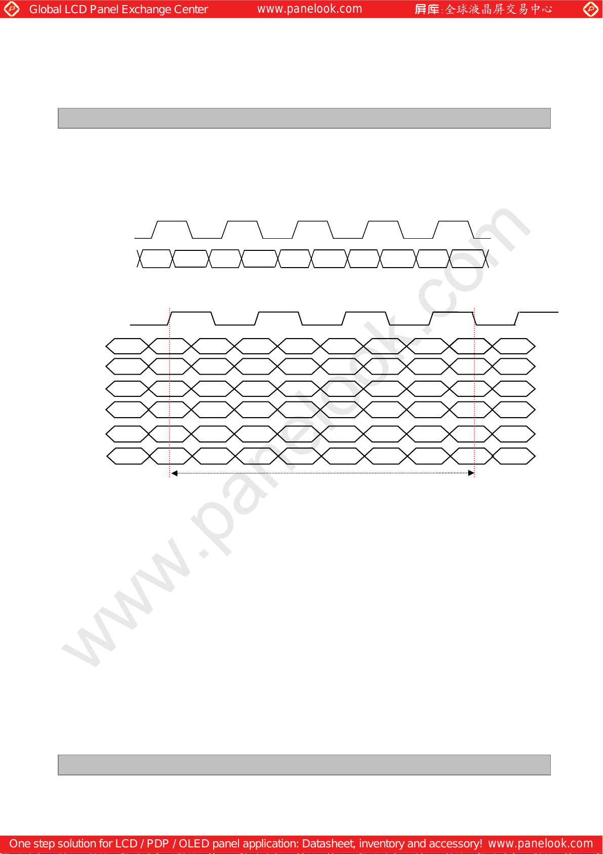
3-4. Data Mapping and Timing
Display data and control signal (RESET) are input to LV0 to LV5.
3-4-1. Control signal input mode
CLK +
LC550MUT
Liquid Crystal Display
Product Specification
LV0 +
RESET RESET RESET RESET RESET RESET RESET RESET RESET RESET
3-4-2. Display data input mode
CLK+
LV0+
LV1+
LV2+
LV3+
LV4+
LV5+
Note :
1. For data mapping, please refer to panel pixel structure Fig.8
D01 D02 D03 D04 D05 D06D00
D11 D12 D13 D14 D15 D16D10 D17
D21 D22 D23 D24 D25 D26D20 D27
D31 D32 D33 D34 D35 D36D30 D37
D41 D42 D43 D44 D45 D46D40 D47
D51 D52 D53 D54 D55 D56D50 D57
DATA INPUT CYCLE
D07 D00
Fig. 7 Mini-LVDS Data
D10
D20
D30
D40
D50
Ver. 0.3
12 /29
Page 14

Global LCD Panel Exchange Center
www.panelook.com
One step solution for LCD / PDP / OLED panel application: Datasheet, inventory and accessory!
www.panelook.com
3-5. Panel Pixel Structure
LC550MUT
Liquid Crystal Display
Product Specification
G1
G2
G3
G4
G5
G6
…….
D1 D2 D3 D4 D5 D1917 D1918 D1919 D1920 D1921
…….
G1078
G1079
G1080
Ver. 0.3
FIG. 8 Panel Pixel Structure
13 /29
Page 15

Global LCD Panel Exchange Center
www.panelook.com
One step solution for LCD / PDP / OLED panel application: Datasheet, inventory and accessory!
www.panelook.com
3-6. Power Sequence
3-6-1. LCD Driving circuit
LC550MUT
Liquid Crystal Display
Product Specification
Power Supply For LCD VCC
Power Supply For LCD
VDD, HVDD, VGH,
Gamma Ref. Voltage
Power Supply For LCD
VGL
GSC and GOE Signal
Power for LED
0V
0V
GSC
GOE
70%
50%
T1
T4
T2
VGH=Vcc
100%
Don’t care
T7
50% 50%
......
......
..
T3
T5
LED ON
T5’
50%
30%
30%
T6
Table 7. POWER SEQUENCE
Parameter
T1 0.5 - ms
T2 0.01
T3 5
T4 0 T2 ms
T5 / T5’ 500 - ms
T7 0.5 - s
Note : 1. Power sequence for Source D-IC must follow the Case1 & 2.
Min Typ Max
Value
Ta= 25±2°C, fV=240Hz, Dclk=74.25MHz
-
-
※ Please refer to Appendix V for more details.
2. The Gate D-IC power on sequence must be VCC, VGL, logic input & VGH.
3. The 1ststart of GSC is located between VGL and VGH.
4. GOE rising is before GSC.
5. Power off sequence order is reverse of power on sequence.
Ver. 0.3
Unit Notes
ms
ms
sec-2T6
14 /29
Page 16

Global LCD Panel Exchange Center
www.panelook.com
One step solution for LCD / PDP / OLED panel application: Datasheet, inventory and accessory!
www.panelook.com
Liquid Crystal Display
Product Specification
4. Optical Specification
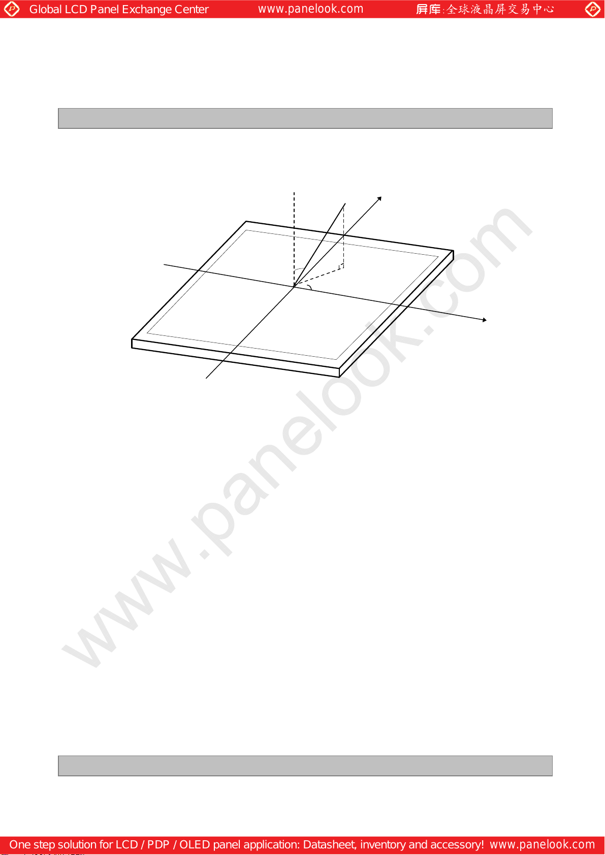
Optical characteristics are determined after the unit has been ‘ON’ and stable in a dark environment at 25±2°C.
The values specified are at an approximate distance 50cm from the LCD surface at a viewing angle of Φ and θ
equal to 0 °.
FIG. 1 shows additional information concerning the measurement equipment and method.
LC550MUT
Optical Stage(x,y)
LCD Module
FIG. 1 Optical Characteristic Measurement Equipment and Method
Table 2. OPTICAL CHARACTERISTICS
Contrast Ratio
Response Time
Color Coordinates
[CIE1931]
Viewing Angle (CR>10)
Falling
RED
GREEN
BLUE
Pritchard 880 or
equivalent
50cm
Ta= 25±2°C, VDD,VGH,VGL=typ., fV=240Hz, Dclk=297MHz
Value
SymbolParameter
NoteUnit
MaxTypMin
CR
TrRising
Tf
Rx
Ry
Gx
Gy
Bx
By
Typ
-0.03
1400(TBD)
5(TBD)
5(TBD)
0.651
(TBD)
0.334
(TBD)
0.312
(TBD)
0.598
(TBD)
0.150
(TBD)
0.068
(TBD)
-
Typ
+0.03
2
2ms
With only color
filter glass
x axis, right(φ=0°)
x axis, left (φ=180°)
y axis, up (φ=90°)
y axis, down (φ=270°)
Ver. 0.3
--89θr
--89θl
--89θu
--89θd
--- 4Gray Scale
3degree
15 /29
Page 17

Global LCD Panel Exchange Center
www.panelook.com
One step solution for LCD / PDP / OLED panel application: Datasheet, inventory and accessory!
www.panelook.com
Product Specification
Notes :1. Contrast Ratio(CR) is defined mathematically as :
LC550MUT
Liquid Crystal Display
CR =
Surface Luminance at position n with all black pixels
n = the Position number(1, 2, 3, 4, 5). For more information, see FIG 2.
2. Response time is the time required for the display to transition from G(0) to G(255) (Rise Time, TrR)
and from G(0) to G(255) (Decay Time, TrD). For additional information see the FIG. 3.
3. Viewing angle is the angle at which the contrast ratio is greater than 10. The angles are
determined for the horizontal or x axis and the vertical or y axis with respect to the z axis which
is normal to the LCD module surface. For more information, see the FIG. 4.
4. Gray scale specification
Gamma Value is approximately 2.2. For more information, see the Table 3.
Table 3. GRAY SCALE SPECIFICATION
Surface Luminance at position n with all white pixels
Gray Level
L0
L63
L127
L191
L255
L319
L383
L447
L511
L575
L639
L703
L767
L831
L895
L959
L1023
Luminance [%] (Typ.)
0.07
0.27
1.04
2.49
4.68
7.66
11.5
16.1
21.6
28.1
35.4
43.7
53.0
63.2
74.5
86.7
100
Positive
Voltage
Negative
Voltage
Gray Level
L0
L63
L127
L191
L223
L255
L255
L223
L191
L127
L63
L0
Gamma Ref.
Gamma9
Gamma6
Gamma5
Gamma4
Gamma3
Gamma1
Gamma18
Gamma16
Gamma15
Gamma14
Gamma13
Gamma10
Ver. 0.3
16 /29
Page 18

Global LCD Panel Exchange Center
www.panelook.com
One step solution for LCD / PDP / OLED panel application: Datasheet, inventory and accessory!
www.panelook.com
Measuring point for surface luminance & measuring point for luminance variation.
LC550MUT
Liquid Crystal Display
Product Specification
H
A
③②
V
①
B
A : H / 4 mm
④
FIG. 9 5 Points for Luminance Measure
Response time is defined as the following figure and shall be measured by switching the input signal for
“Gray(0)” and “Gray(255)”.
TrR
100
90
⑤
TrD
B : V / 4 mm
@ H,V : Active Area
Optical
Response
Ver. 0.3
10
0
Gray(0)
N,M = Black~White, N<M
FIG. 10 Response Time
Gray(255)
Gray(0)
17 /29
Page 19
Global LCD Panel Exchange Center
www.panelook.com
One step solution for LCD / PDP / OLED panel application: Datasheet, inventory and accessory!
www.panelook.com
Dimension of viewing angle range
LC550MUT
Liquid Crystal Display
Product Specification
φ
= 180°, Left
φ
= 270°, Down
Normal
E
θ
φ
FIG. 11 Viewing Angle
Y
φ
= 90°, Up
φ
= 0°, Right
Ver. 0.3
18 /29
Page 20

Global LCD Panel Exchange Center
www.panelook.com
One step solution for LCD / PDP / OLED panel application: Datasheet, inventory and accessory!
www.panelook.com
5. Mechanical Characteristics
Table 10 provides general mechanical characteristics.
Table 10. MECHANICAL CHARACTERISTICS
Outline Dimension
(Only Glass)
LC550MUT
Liquid Crystal Display
Product Specification
ValueItem
1220.8 mmHorizontal
693.8 mmVertical
1.94 mmThickness
1220.8 mmHorizontal
Bezel Area
693.8 mmVertical
1209.6 mmHorizontal
Active Display Area
680.4 mmVertical
3.4Kg (Typ.)Weight
Note : Please refer to a mechanic drawing in terms of tolerance at the next page.
Ver. 0.3
19 /29
Page 21

Global LCD Panel Exchange Center
www.panelook.com
One step solution for LCD / PDP / OLED panel application: Datasheet, inventory and accessory!
www.panelook.com
<FRONT VIEW>
LC550MUT
Liquid Crystal Display
Product Specification
Ver. 0.3
20 /29
Page 22

Global LCD Panel Exchange Center
www.panelook.com
One step solution for LCD / PDP / OLED panel application: Datasheet, inventory and accessory!
www.panelook.com
6. Reliability
Table 11. ENVIRONMENT TEST CONDITION
LC550MUT
Liquid Crystal Display
Product Specification
ConditionTest ItemNo.
Ta= 60°C 240h High temperature storage test1
Ta= -20°C 240hLow temperature storage test2
Ta= 50°C 50%RH 240hHigh temperature operation test3
Altitude operating
6
storage / shipment
Ta= 0°C 240hLow temperature operation test4
Ta= 40 °C ,90%RHHumidity condition Operation5
0 - 15,000 ft
0 - 40,000 ft
Ver. 0.3
21 /29
Page 23

Global LCD Panel Exchange Center
www.panelook.com
One step solution for LCD / PDP / OLED panel application: Datasheet, inventory and accessory!
www.panelook.com
7. International Standards
7-1. Environment
a) RoHS, Directive 2002/95/EC of the European Parliament and of the council of 27 January 2003
LC550MUT
Liquid Crystal Display
Product Specification
Ver. 0.3
22 /29
Page 24

Global LCD Panel Exchange Center
www.panelook.com
One step solution for LCD / PDP / OLED panel application: Datasheet, inventory and accessory!
www.panelook.com
8. Packing
8-1. Packing Form
a) Package quantity in one Pallet : 70 pcs
b) Pallet Size :1400 mm(L) X 900 mm(W) X 1105 mm(H)
LC550MUT
Liquid Crystal Display
Product Specification
Ver. 0.3
23 /29
Page 25

Global LCD Panel Exchange Center
www.panelook.com
One step solution for LCD / PDP / OLED panel application: Datasheet, inventory and accessory!
www.panelook.com
9. Precautions
Please pay attention to the followings when you use this TFT LCD panel.
9-1. Assembly Precautions
(1) Please attach the surface transparent protective plate to the surface in order to protect the polarizer.
Transparent protective plate should have sufficient strength in order to the resist external force.
(2) You should adopt radiation structure to satisfy the temperature specification.
(3) Acetic acid type and chlorine type materials for the cover case are not desirable because the former
generates corrosive gas of attacking the polarizer at high temperature and the latter causes circuit break
by electro-chemical reaction.
(4) Do not touch, push or rub the exposed polarizers with glass, tweezers or anything harder than HB
pencil lead. And please do not rub with dust clothes with chemical treatment.
Do not touch the surface of polarizer for bare hand or greasy cloth.(Some cosmetics are detrimental
to the polarizer.)
(5) When the surface becomes dusty, please wipe gently with absorbent cotton or other soft materials like
chamois soaks with petroleum benzine. Normal-hexane is recommended for cleaning the adhesives
used to attach front / rear polarizers. Do not use acetone, toluene and alcohol because they cause
chemical damage to the polarizer
(6) Wipe off saliva or water drops as soon as possible. Their long time contact with polarizer causes
deformations and color fading.
(7) Board ass’y should be put on the mold frame properly.
(8) FFC Cable should be connected between System board and Source PCB correctly.
(9) Mechanical structure for backlight system should be designed for sustaining board ass’y safely.
LC550MUT
Liquid Crystal Display
Product Specification
9-2. Operating Precautions
(1) The spike noise causes the mis-operation of circuits. It should be lower than following voltage :
V=±200mV(Over and under shoot voltage)
(2) Response time depends on the temperature.(In lower temperature, it becomes longer.)
(3) Brightness depends on the temperature. (In lower temperature, it becomes lower.)
And in lower temperature, response time(required time that brightness is stable after turned on)
becomes longer
(4) Be careful for condensation at sudden temperature change.Condensation makes damage to polarizer or
electrical contacted parts. And after fading condensation, smear or spot will occur.
(5) When fixed patterns are displayed for a long time, remnant image is likely to occur.
(6) Module has high frequency circuits. Sufficient suppression to the electromagnetic interference shall be
done by system manufacturers. Grounding and shielding methods may be important to minimized the
interference.
(7) Please do not give any mechanical and/or electrical impact to board assy. Otherwise, it can’t be operated
its full characteristics perfectly.
Ver. 0.3
24 /29
Page 26

Global LCD Panel Exchange Center
www.panelook.com
One step solution for LCD / PDP / OLED panel application: Datasheet, inventory and accessory!
www.panelook.com
9-3. Electrostatic Discharge Control
Since a module is composed of electronic circuits, it is not strong to electrostatic discharge. Make certain that
treatment persons are connected to ground through wrist band etc. And don’t touch interface pin directly.
Panel ground path should be connected to metal ground.
9-4. Precautions for Strong Light Exposure
Strong light exposure causes degradation of polarizer and color filter.
9-5. Storage
LC550MUT
Liquid Crystal Display
Product Specification
When storing the board ass’y as spares for a long time, the following precautions are necessary.
(1) Store them in a dark place. Do not expose the board ass’y to sunlight or fluorescent light. Keep the
temperature between 5°C and 35°C at normal humidity.
(2) The polarizer surface should not come in contact with any other object.
It is recommended that they be stored in the container in which they were shipped.
Ver. 0.3
25 /29
Page 27

Global LCD Panel Exchange Center
www.panelook.com
One step solution for LCD / PDP / OLED panel application: Datasheet, inventory and accessory!
www.panelook.com
# APPENDIX- I
■ Pallet Ass’y
LC550MUT
Liquid Crystal Display
Product Specification
S
h
o
u
l
d
b
e
U
d
e
t
a
d
p
No. Description Material
ⓐ
ⓑ
Pallet Plywood
Carton Plate Single Wall
ⓒ
ⓓ
ⓔ
ⓕ
ⓖ
ⓗ
ⓘ
Ver. 0.3
PE Sheet Carbon
Top Packing EPP
Bottom Packing EPP
Angle Packing Single Wall
Tape OPP
Band PP
Clip Steel
26 /29
Page 28
Global LCD Panel Exchange Center
www.panelook.com
One step solution for LCD / PDP / OLED panel application: Datasheet, inventory and accessory!
www.panelook.com
# APPENDIX- II
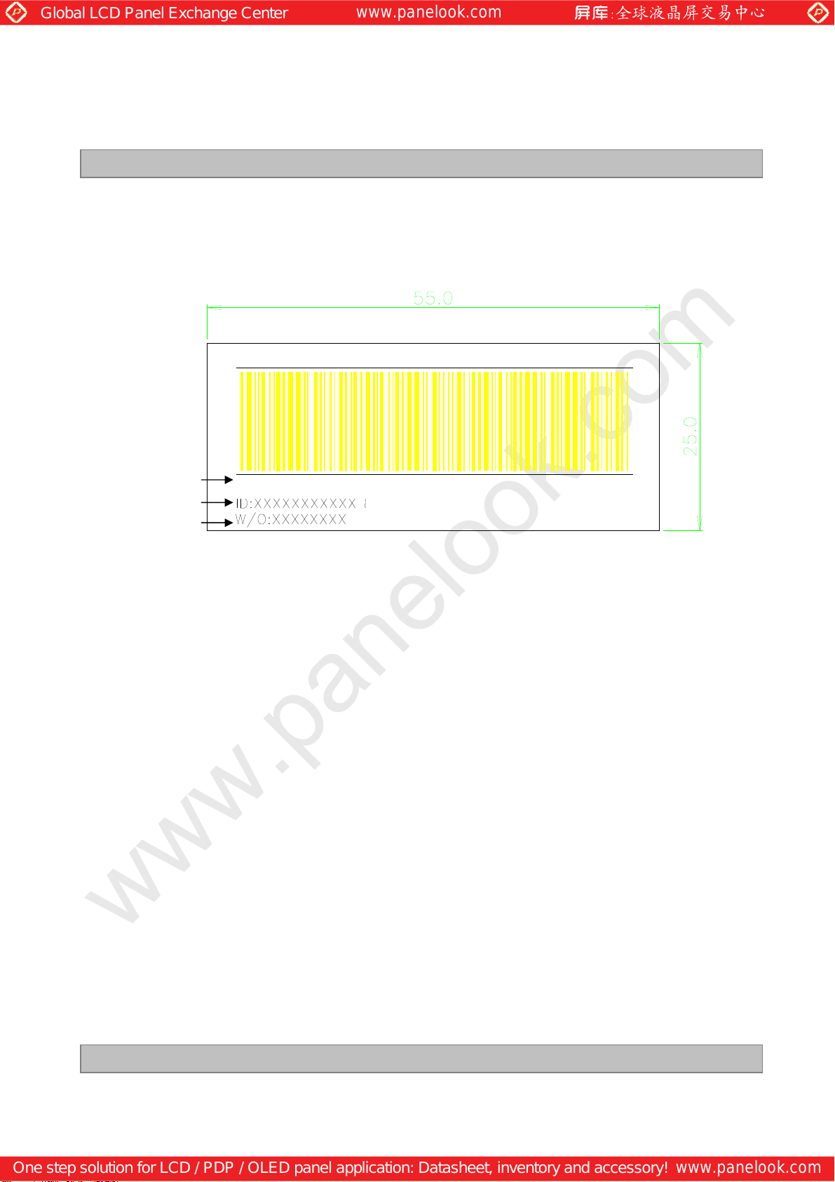
■ Serial Label
LC550MUT
Liquid Crystal Display
Product Specification
Model
Serial No.
Work Other
LC550MUT-SCA1
XXXX
Ver. 0.3
27 /29
Page 29

Global LCD Panel Exchange Center
www.panelook.com
One step solution for LCD / PDP / OLED panel application: Datasheet, inventory and accessory!
www.panelook.com
LC550MUT
Liquid Crystal Display
# APPENDIX 3# APPENDIX 3
# APPENDIX- III
■ Pallet Label
Product Specification
LC550MUT
SCA1
10 PCS
MADE IN KOREA
001/01-01
XXXXXXXXXXXXX XXX
RoHS Verified
Ver. 0.3
28 /29
Page 30

Global LCD Panel Exchange Center
www.panelook.com
One step solution for LCD / PDP / OLED panel application: Datasheet, inventory and accessory!
www.panelook.com
# APPENDIX- IV
■ LC550MUT-SCA1-Source D-IC Power Sequence
LC550MUT
Liquid Crystal Display
Product Specification
- Input Signal : SOE,POL,GSP,H_CONV,OPT_N
Ver. 0.3
29 /29
 Loading...