

Page 1
( ) Preliminary Specification
(●) Final Specification
Title 55.0” WUXGA TFT LCD
LC550EUG
Product Specification
SPECIFICATION
FOR
APPROVAL
BUYER LGE
MODEL
APPROVED BY
/
/
/
SIGNATURE
DATE
SUPPLIER LG Display Co., Ltd.
*MODEL LC550EUG
SUFFIX PFF1 (RoHS Verified)
APPROVED BY
H. S. Song / Team Leader
REVIEWED BY
D. W. Lee / Project Leader
PREPARED BY
C. H. Yu / Engineer
SIGNATURE
DATE
Please return 1 copy for your confirmation with
your signature and comments.
Ver. 1.0
TV Product Development Dept.
LG Display Co., Ltd.
1 /37
Page 2
Product Specification
CONTENTS
LC550EUG
Number ITEM
COVER
CONTENTS
RECORD OF REVISIONS 3
1 GENERAL DESCRIPTION
2 ABSOLUTE MAXIMUM RATINGS
3 ELECTRICAL SPECIFICATIONS
3-1 ELECTRICAL CHARACTERISTICS
3-2 INTERFACE CONNECTIONS
3-3 SIGNAL TIMING SPECIFICATIONS
3-4 PANEL PIXEL STRUCTURE
3-5 POWER SEQUENCE
4 OPTICAL SPECIFICATIONS
5 MECHANICAL CHARACTERISTICS
6 RELIABILITY
Page
1
2
4
5
6
6
9
12
13
14
15
21
24
7 INTERNATIONAL STANDARDS
7-1 SAFETY
7-2 EMC 25
7-3 Environment
8 PACKING
8-1 DESIGNATION OF LOT MARK
8-2 PACKING FORM
9 PRECAUTIONS 27
9-1 MOUNTING PRECAUTIONS 27
9-2 OPERATING PRECAUTIONS
9-3 ELECTROSTATIC DISCHARGE CONTROL 28
9-4 PRECAUTIONS FOR STRONG LIGHT EXPOSURE
9-5 STORAGE 28
9-6 OPERAGING CONDITION GUIDE 28
Ver. 1.0
25
25
25
26
26
26
28
28
2 /37
Page 3
Product Specification
RECORD OF REVISIONS
Revision No. Revision Date Page Description
0.0 AUG, 15, 2012 - Preliminary Specification (First Draft)
0.1 Oct. 29. 2012 - Updated TBD Spec.
22,23 Updated LCM mechanical drawing.
0.2 Nov. 27. 2012 15 Updated Color Coordinates
32 Updated LED Spec.
Final Draft.-Dec, 13, 20121.0
LC550EUG
Ver. 1.0
3 /37
Page 4
LC550EUG
Product Specification
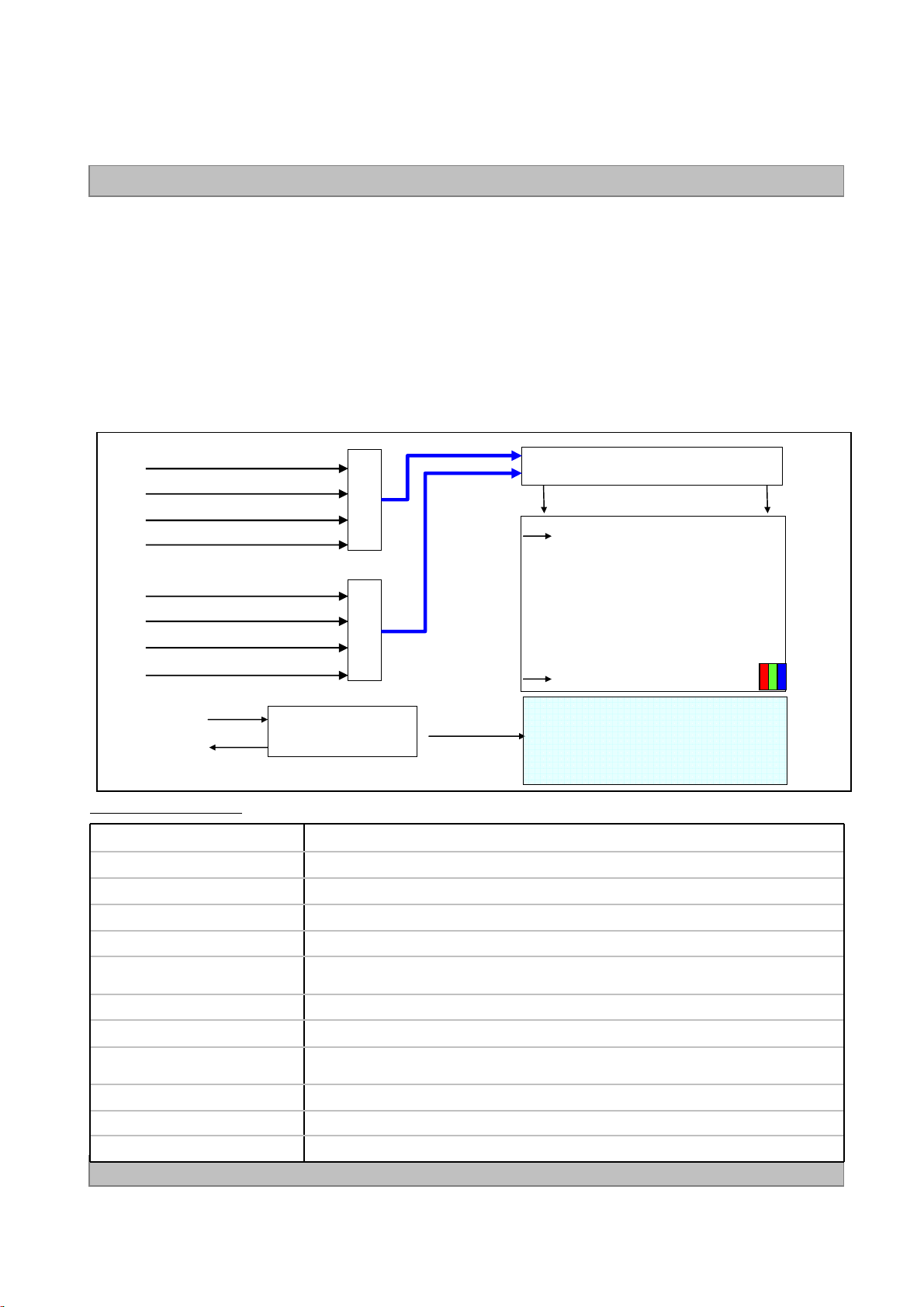
1. General Description
The LC550EUG is a Color Active Matrix Liquid Crystal Display with an integral Light Emitting Diode (LED)
bac k li ght s y st em. T h e m a tr i x em plo ys a - Si T h in Fi l m T ra n s is t or as th e a c tiv e e lem e nt.
It is a transmissive display type which is operating in the normally black mode. It has a 54.64 inch diagonally
measured active display area with WUXGA resolution (1080 vertical by 1920 horizontal pixel array).
Each pixel is divided into Red, Green and Blue sub-pixels or dots which are arrayed in vertical stripes.
Gray scale or the luminance of the sub-pixel color is determined with a 8-bit gray scale signal for each dot.
Therefore, it can present a palette of more than 16.7M(true) colors.
It is intended to support LCD TV, PCTV where high brightness, super wide viewing angle, high color gamut,
high color depth and fast response time are important.
Power (VCC, VDD, HVDD, VGH, VGL)
Gate Control Signal
Gamma Reference Voltage
EPI (RGB & Control signal) for Left drive
Power (VCC, VDD, HVDD, VGH, VGL)
Gate Control Signal
Gamma Reference Voltage
EPI (RGB & Control Signal) for Right drive
LED Anode
LED Cathode
CN201 (8Pin)
CN202 (8pin)
CN1
(50pin)
CN2
(50pin)
S1 S1920
G1
G1080
Source Driver Circuit
TFT - LCD Panel
(1920 × RGB × 1080 pixels)
[Gate In Panel]
Back light Assembly
General Features
Active Screen Size 54.64 inches(1387.80mm) diagonal
Outline Dimension
Pixel Pitch 0.630 mm x 0.630 mm
Pixel Format 1920 horiz. by 1080 vert. Pixels, RGB stripe arrangement
Color Depth 8-bit, 16.7 M colors (※ 1.06B colors @ 10 bit (D) System Output )
Drive IC Data Interface
Luminance, White 400cd/m2 (Center 1point ,Typ.)
1229.4 X 706.3 X 9.9(B)/21.9(D)
Source D-IC : 8-bit EPI, gamma reference voltage, and control signals
Gate D-IC : Gate In Panel
Viewing Angle (CR>10) Viewing angle free ( R/L 178 (Min.), U/D 178 (Min.))
Power Consumption
Weight 15.0Kg (Typ.)
Display Mode Transmissive mode, Normally black
Surface Treatment Hard coating(2H), Anti-glare treatment of the front polarizer (Haze < 1%)
Ver. 1.0
Total 81.58 W (Typ.) (Logic= 7.28 W with T-CON
LED Backlight=74.3W ( IF_cathode=150 mA)
4 /37
Page 5
LC550EUG
Product Specification
2. Absolute Maximum Ratings
The following items are maximum values which, if exceeded, may cause faulty operation or permanent damage
to the LCD module.
Table 1. ABSOLUTE MAXIMUM RATINGS
Parameter Symbol
Min Max
Logic & EPI Power Voltage VCC -0.5 +2.2 VDC
Gate High Voltage VGH +18.0 +30.0 VDC
Gate Low Voltage VGL -8.0 -4.0 VDC
Value
Unit Note
Source D-IC Analog Voltage VDD -0.3 +18.0 VDC
Gamma Ref. Voltage (Upper) VGMH ½VDD-0.5 VDD+0.5 VDC
Gamma Ref. Voltage (Low) VGML -0.3 ½ VDD+0.5 VDC
LED Input Voltage VF - +97.5 VDC
Panel Front Temperature TSUR - +68 °C 4
Operating Temperature TOP 0 +50 °C
Storage Temperature TST -20 +60 °C
Operating Ambient Humidity HOP 10 90 %RH
Storage Humidity HST 10 90 %RH
Note
1. Ambient temperature condition (Ta = 25 ± 2 °C )
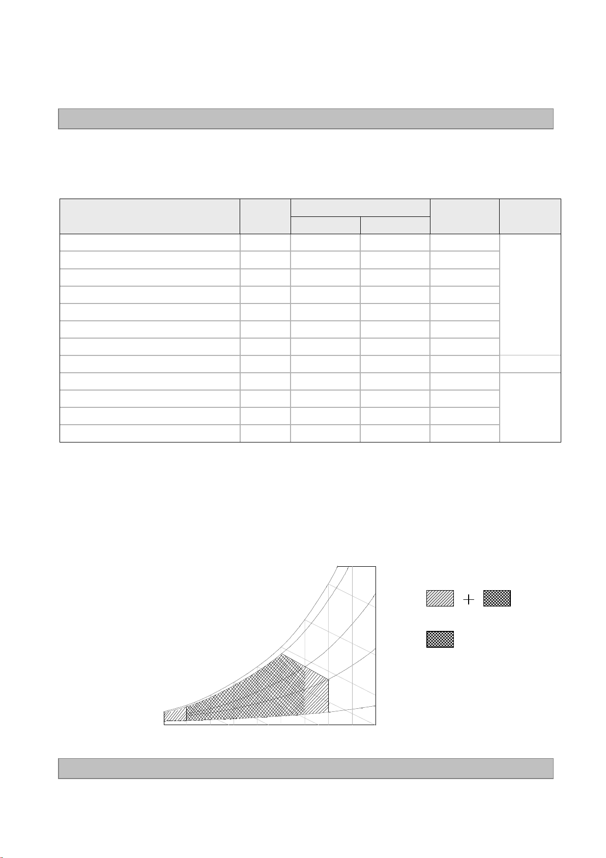
2. Temperature and relative humidity range are shown in the figure below.
Wet bulb temperature should be Max 39°C, and no condensation of water.
3. Gravity mura can be guaranteed below 40°C condition.
4. The maximum operating temperatures is based on the test condition that the surface temperature
of display area is less than or equal to 68°C with LCD module alone in a temperature controlled chamber.
Thermal management should be considered in final product design to prevent the surface temperature of
display area from being over 68℃. The range of operating temperature may be degraded in case of
improper thermal management in final product design.
90%
60
60%
1
2,3
Ver. 1.0
Wet Bulb
Temperature [°C]
20
10
0
10 20 30 40 50 60 70 800-20
Dry Bulb Temperature [°C]
30
40
50
40%
10%
Storage
Operation
Humidity [(%)RH]
5 /37
Page 6
LC550EUG
Product Specification
3. Electrical Specifications
3-1. Electrical Characteristics
It requires several power inputs. The VCC is the basic power of LCD Driving power sequence, Which is used
to logic power voltage of Source D-IC and GIP.
Table 2. ELECTRICAL CHARACTERISTICS
Parameter Symbol Condition MIN TYP MAX Unit Note
Logic Power Voltage VCC - 1.62 1.8 1.98
Logic High Level Input Voltage VIH - 1.4 - VCC
Logic Low Level Input Voltage VIL - 0 - 0.4
Source D-IC Analog Voltage VDD - 15.8 16.0 16.2
Half Source D-IC Analog
Voltage
Gamma Reference Voltage
Common Voltage Vcom Reverse 6.75 7.05 7.35 V
EPI input common voltage VCM LVDS Type 0.8 VCC/2 1.3 V
EPI input differential voltage Vdiff - 150 - 500 mV
EPI Input eye diagram Veye - 90 - - mV
Gate High Voltage VGH
Gate Low Voltage VGL
GIP Bi-Scan Voltage
GIP Refresh Voltage
GIP Start Pulse Voltage VST - VGL - VGH V
GIP Operating Clock GCLK - VGL - VGH V
Total Power Current
Total Power Consumption
H_VDD - 7.8 8.0 8.2
V
GMH
V
GML
VGI_P - VGL - - VDC
VGI_N - - - VGH VDC
VGH
even/odd
ILCD - - 607 758 mA 1
PLCD - - 7.28 9.1 Watt 1
(GMA1 ~ GMA9) H_VDD+0.2V - VDD-0.2
(GMA10 ~ GMA18) 0.2 - H_VDD-0.2V
@ 25℃ 27.7 28 28.3 VDC
@ 0℃ 29.7 30 30.3 VDC
-
- VGL - VGH V
-6.8 -7 -7.2 VDC
VDC
VDC
VDC
VDC
VDC 6
VDC
VDC
5
Note:
Ver. 1.0
1. The specified current and power consumption are under the VLCD=12V., 25 ± 2°C, fV=60Hz
condition whereas mosaic pattern(8 x 6) is displayed and fVis the frame frequency.
2. The above spec is based on the basic model.
3. All of the typical gate voltage should be controlled within 1% voltage level
4. Ripple voltage level is recommended under ±5% of typical voltage
5. In case of EPI signal spec, refer to Fig 2 for the more detail.
6. HVDD Voltage level is half of VDD and it should be between Gamma9 and Gamma10.
6 /37
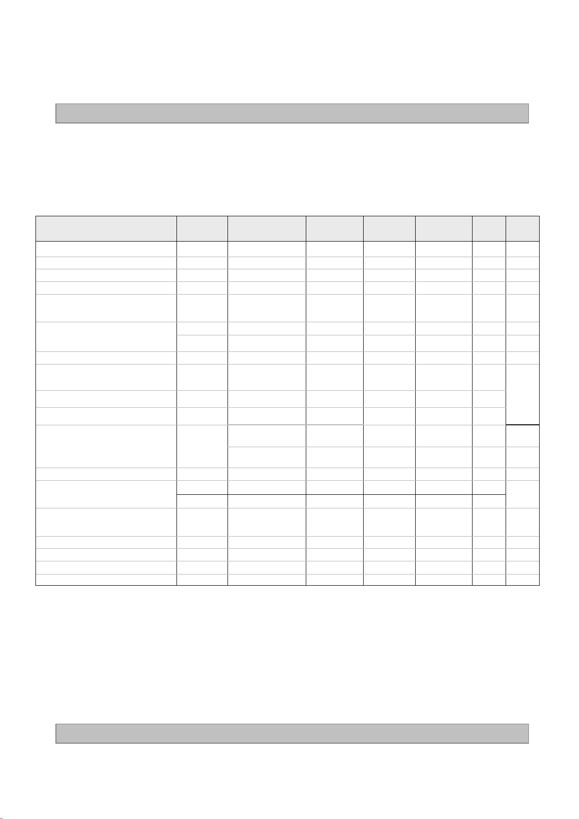
Page 7
VGH
VGHM
GND
VGL
LC550EUG
Product Specification
Without GPM With GPM
FIG. 1 Gate Output Wave form without GPM and with GPM
EPI +
0 V
0 V
Vdiff
Vdiff
(Differential Probe)
(Differential Probe)
(Differential Probe)(Differential Probe)
FIG. 2-1 EPI Differential signal characteristics
EPI -
0 V
1 UI
0.5 UI
B1 B2
(Differential Probe)
(Differential Probe)
(Differential Probe)(Differential Probe)
FIG. 2-2 Eye Pattern of EPI Input
Vdiff
(Active Probe)
(Active Probe)
(Active Probe)(Active Probe)
Vcm
Veye
Veye
Ver. 1.0
****Source PCB
Source PCB
Source PCBSource PCB
FIG. 3 Measure point
7 /37
Page 8
Product Specification
Table 3. ELECTRICAL CHARACTERISTICS (Continue)
LC550EUG
Parameter Symbol
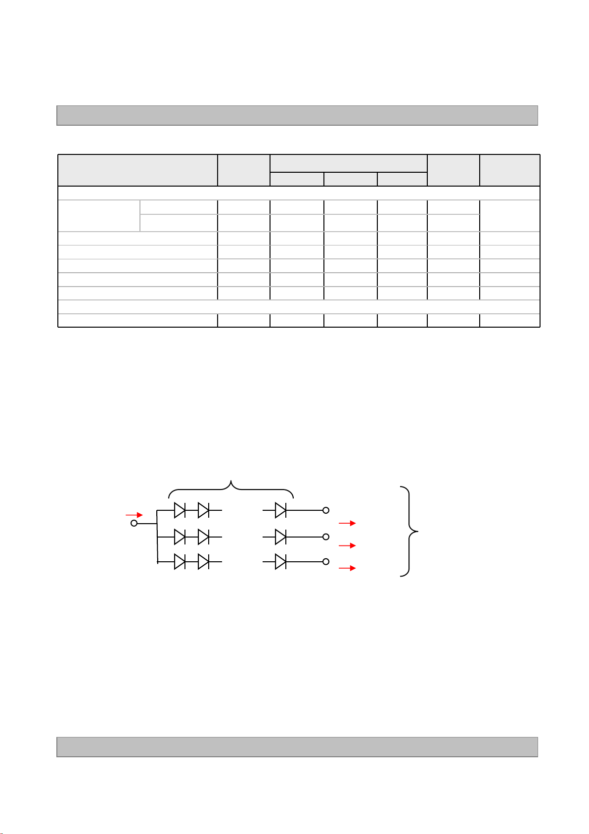
Backlight Assembly :
Forward Current
(one array)
Forward Voltage V
Forward Voltage Variation △V
Power Consumption P
Burst Dimming Duty On duty 1 100 %
Burst Dimming Frequency 1/T 95 182 Hz 8
LED Array :
Life Time 30,000 50,000 Hrs 7
The design of the LED driver must have specifications for the LED array in LCD Assembly.
Note :
Anode I
Cathode I
F (anode)
F (cathode)
F
F
BL
Min Typ Max
142.5 150 157.5 mAdc
75.0 82.5 87.5 Vdc 4
Values
450 mAdc
1.7 Vdc 5
74.3 78.8 W 6
Unit Note
The electrical characteristics of LED driver are based on Constant Current driving type.
The performance of the LED in LCM, for example life time or brightness, is extremely influenced by the
characteristics of the LED Driver. So, all the parameters of an LED driver should be carefully designed.
When you design or order the LED driver, please make sure unwanted lighting caused by the mismatch of the
LED and the driver (no lighting, flicker, etc) has never been occurred. When you confirm it, the LCD–
Assembly should be operated in the same condition as installed in your instrument.
1. Electrical characteristics are based on LED Array specification.
2. Specified values are defined for a Backlight Assembly. (IBL : 2 LED array/LCM)
3.Each LED array has one anode terminal and 3 cathode terminals.
The forward current(IF) of the anode terminal is 450mA and it supplies 150mA into 3 strings, respectively
±5%
2, 3
1string(25 LED PKG)
450mA
Anode#1
° ° °
° ° °
° ° °
Cathode #1
150mA
Cathode #2
150mA
Cathode #3
150mA
1 Array (3 Strings)
4. The forward voltage(VF) of LED array depends on ambient temperature (Appendix-V)
5. ΔVFmeans Max VF-Min VFin one Backlight. So VFvariation in a Backlight isn’t over Max. 1.7V
6. Maximum level of power consumption is measured at initial turn on.
Typical level of power consumption is measured after 1hrs aging at 25 ± 2°C.
7. The life time(MTTF) is determined as the time at which brightness of the LED is 50% compared to that of
initial value at the typical LED current on condition of continuous operating at 25 ± 2°C, based on duty 100%.
8. The reference method of burst dimming duty ratio.
It is recommended to use synchronous V-sync frequency to prevent waterfall
(Vsync x 2 =Burst Frequency)
Though PWM frequency is over 182Hz (max252Hz), function of backlight is not affected.
Ver. 1.0
8 /37
Page 9
LC550EUG
Product Specification
3-2. Interface Connections
This LCD module employs two kinds of interface connection, two 50-pin FFC connector are used for the
module electronics and 8-pin / 8-pin connectors are used for the integral backlight system.
3-2-1. LCD Module
-LCD Connector (CN1): TF06L-50S-0.5SH (Manufactured by HRS) or Compatible
Table 3-1. MODULE CONNECTOR(CN1) PIN CONFIGURATION
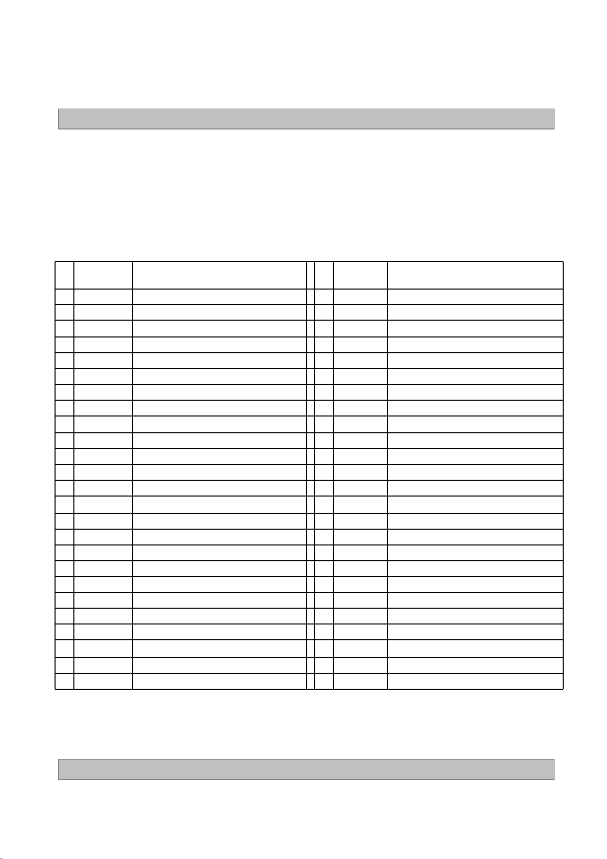
No Symbol Description No Symbol Description
1 LTD_OUT LTD OUTPUT 26 GND Ground
2 NC No Connection 27 EPI2- EPI Receiver Signal(2-)
3 GCLK1 GIP GATE Clock 1 28 EPI2+ EPI Receiver Signal(2+)
4 GCLK2 GIP GATE Clock 2 29 GND Ground
5 GCLK3 GIP GATE Clock 3 30 GND Ground
6 GCLK4 GIP GATE Clock 4 31 EPI1- EPI Receiver Signal(1-)
7 GCLK5 GIP GATE Clock 5 32 EPI1+ EPI Receiver Signal(1+)
8 GCLK6 GIP GATE Clock 6 33 GND Ground
9 VGI_N GIP Bi-Scan (VGI_N = VGH) 34 VCC
10 VGI_P GIP Bi-Scan (VGI_P = VGL) 35 Vterm Vterm Power Voltage
11 VGH_ODD GIP Panel VDD for Odd GATE TFT 36 LOCKOUT3 LOCKOUT3
12 VGH_EVEN GIP Panel VDD for Even GATE TFT 37 NC No Connection
13 VGL GATE Low Voltage 38 GND Ground
14 VST VERTICAL START PULSE 39 GMA 18 GAMMA VOLTAGE 18 (Output From LCD)
15 GIP_Reset GIP Reset 40 GMA 16 GAMMA VOLTAGE 16
16 VCOM_L_FB VCOM Left Feed-Back Output 41 GMA 15 GAMMA VOLTAGE 15
17 VCOM_L VCOM Left Input 42 GMA 14 GAMMA VOLTAGE 14
18 GND Ground 43 GMA 12 GAMMA VOLTAGE 12
19 VDD Driver Power Supply Voltage 44 GMA 10 GAMMA VOLTAGE 10 (Output From LCD)
20 VDD Driver Power Supply Voltage 45 GMA 9 GAMMA VOLTAGE 9 (Output From LCD)
21 H_VDD Half Driver Power Supply Voltage 46 GMA 7 GAMMA VOLTAGE 7
22 GND Ground 47 GMA 5 GAMMA VOLTAGE 5
23 EPI3- EPI Receiver Signal(3-) 48 GMA 4 GAMMA VOLTAGE 4
24 EPI3+ EPI Receiver Signal(3+) 49 GMA 3 GAMMA VOLTAGE 3
25 GND Ground 50 GMA 1 GAMMA VOLTAGE 1(Output From LCD)
Logic & EPI Power Voltage
Note :
1. Please refer to application note for details.
(GIP & Half VDD & Gamma Voltage setting)
Ver. 1.0
9 /37
Page 10
Product Specification
-LCD Connector (CN1): TF06L-50S-0.5SH (Manufactured by HRS) or Compatible
Table 3-2. MODULE CONNECTOR(CN2) PIN CONFIGURATION
No Symbol Description No Symbol Description
LC550EUG
1 GMA 1 GAMMA VOLTAGE 1 (Output From LCD)
2 GMA 3 GAMMA VOLTAGE 3
3 GMA 4 GAMMA VOLTAGE 4
4 GMA 5 GAMMA VOLTAGE 5
5 GMA 7 GAMMA VOLTAGE 7
6 GMA 9 GAMMA VOLTAGE 9 (Output From LCD)
7 GMA 10 GAMMA VOLTAGE 10 (Output From LCD)
8 GMA 12 GAMMA VOLTAGE 12
9 GMA 14 GAMMA VOLTAGE 14
10 GMA 15 GAMMA VOLTAGE 15
11 GMA 16 GAMMA VOLTAGE 16
12 GMA 18 GAMMA VOLTAGE 18 (Output From LCD)
13 GND Ground
LOCKOUT6 LOCKOUT6 39 VGH_EVEN GIP Panel VDD for Even GATE TFT
14
15
LOCKIN3 LOCKIN3 40 VGH_ODD GIP Panel VDD for Odd GATE TFT
Vterm Vterm Power Voltage 41 VGI_P GIP Bi-Scan (VGI_P = VGL)
16
17 VCC
18
GND Ground 43 GCLK6 GIP GATE Clock 6
EPI6- EPI Receiver Signal(6-) 44 GCLK5 GIP GATE Clock 5
19
20
EPI6+ EPI Receiver Signal(6+) 45 GCLK4 GIP GATE Clock 4
21 GND Ground
22 GND Ground
EPI5- EPI Receiver Signal(5-) 48 GCLK1 GIP GATE Clock 1
23
EPI5+ EPI Receiver Signal(5+) 49 NC No Connection
24
25 GND Ground
Note :
1. Please refer to application note for details.
Logic & EPI Power Voltage
26 GND Ground
27 EPI1- EPI Receiver Signal(4-)
28 EPI1+ EPI Receiver Signal(4+)
29 GND Ground
30 H_VDD Half Driver Power Supply Voltage
31 VDD Driver Power Supply Voltage
32 VDD Driver Power Supply Voltage
33 GND Ground
34 VCOM_R VCOM Right Input
35 VCOM_R_FB VCOM Right Feed-Back Output
36 GIP_Reset GIP Reset
37 VST VERTICAL START PULSE
38 VGL GATE Low Voltage
42 VGI_N GIP Bi-Scan (VGI_N = VGH)
46 GCLK3 GIP GATE Clock 3
47 GCLK2 GIP GATE Clock 2
50 LTD_OUT LTD OUTPUT
(GIP & Half VDD & Gamma Voltage setting)
CN 1
#36
Source Left PCB
Source Right PCB
CN 2
#1 #50
#14
#15
#1 #50
Ver. 1.0
LOCK6
To SOC ( or T-Con)
LTD OUTPUT
LOCK3
System (or Control) PCB
10 /37
Page 11
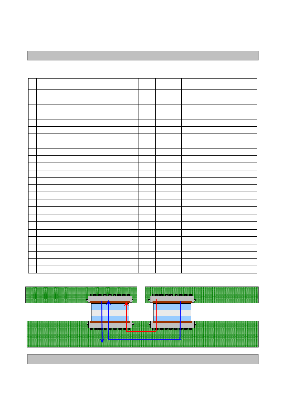
3-2-2. Backlight Module
LC550EUG
Product Specification
[ CN201 ]
1) LED Array assy Connector (Plug)
: HS100-L08N-N62 (black color, manufactured by UJU)
2) Mating Connector (Receptacle)
: IS100-L08T-C46 (black color, manufactured by UJU)
[ CN202 ]
1) LED Array assy Connector (Plug)
: HS100-L08N-N62-A (natural color, manufactured by UJU)
2) Mating Connector (Receptacle)
: IS100-L08T-C46-A (natural color, manufactured by UJU)
Table 4. BACKLIGHT CONNECTOR PIN CONFIGURATION(CN201,CN202)
No Symbol(CN201)
1 L1 Cathode
2 L2 Cathode
3 L3 Cathode
4 N.C
5 N.C
6 N.C
7 N.C
8 Anode_L
Description
LED Output Current
LED Output Current
LED Output Current
Open
Open
Open
Open
LED Input Current for
L1~L3
Note
No Symbol(CN202)
1 Anode_R
2 N.C
3 N.C
4 N.C
5 N.C
6 R1 Cathode
7 R2 Cathode
8 R3 Cathode
Description
LED Input Current for
R1~R3
Open
Open
Open
Open
LED Output Current
LED Output Current
LED Output Current
Note
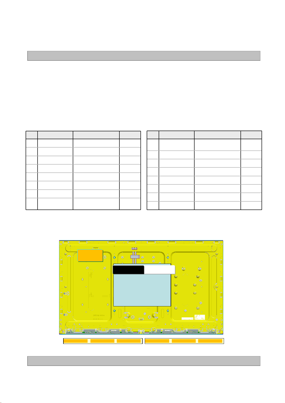
◆ Rear view of LCM
Rear
1
L
Ver. 1.0
87654321
CNT 201 CNT 202
Power Board
Power Board
Power BoardPower Board
2
L
3
L
87654321
1
R
2
R
3
R
11 /37
Page 12
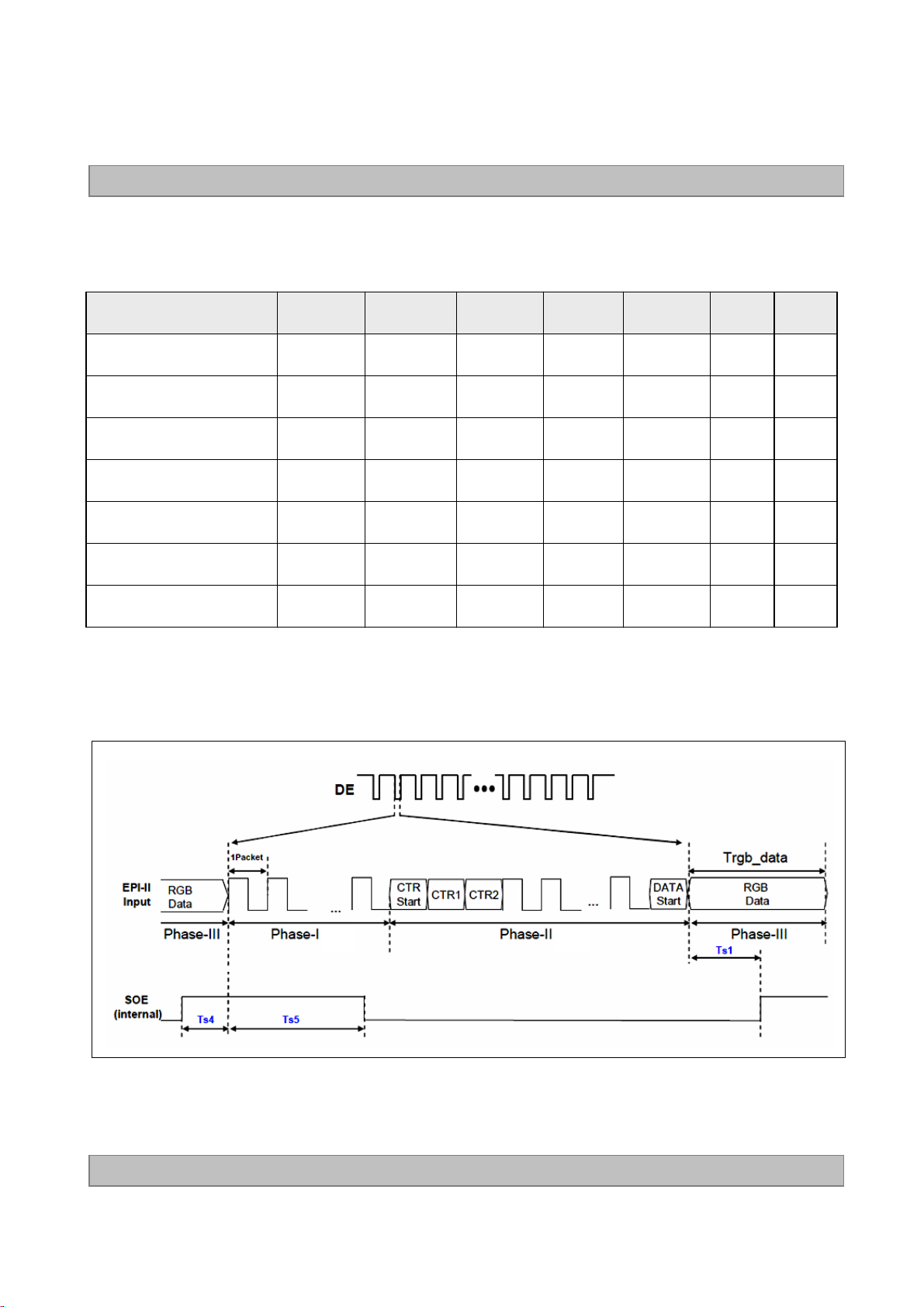
3-3. Signal Timing Specifications
Table 5. Timing Requirements
Parameter Symbol Condition Min Typ Max Unit notes
LC550EUG
Product Specification
Unit Interval
Effective Veye width time
Modulation Ratio of SSC
1stdata to SOE rising time
SOE rising to last data
Last data to SOE falling
EPI Bandwidth
notes :
1. VModulation Ratio of SSC for 20KHz ~ 100kHz Modulation Frequency is calculated by
UI
B1&B2
Vspread
Ts1
Ts4
Ts5
BW
- 1.37 1.44 1.70 ns
- 0.25 - - UI Fig. 2
@100KHz - - 2 % 1
- 3 - - Packet Fig.4
0 - - Packet Fig.4
- 10 - - Packet Fig.4
- 0.588 - 0.728 GBPS
(7 – 0.05*Fmod), where Fmod unit is KHz.
Ver. 1.0
FIG 4. SOE Width & Timing
12 /37
Page 13

3-4. Panel Pixel Structure
D1 D2 D3 D4 D5 D1918 D1919 D1920 D1921
G1
G2
G3
G4
G5
G6
LC550EUG
Product Specification
G1078
G1079
G1080
FIG. 5 Panel Pixel Structure
Ver. 1.0
13 /37
Page 14

3-5. Power Sequence
3-5-1. LCD Driving circuit
Power Supply For LCD VCC
Power Supply For LCD
VDD, HVDD,VGH, Gamma Ref.
Voltage
Power Supply For LCD
VGL
0V
0V
Product Specification
70%
50%
100%
T1
T2
VGH
90%
LC550EUG
T7
GIP Signal For LCD
Power For LED
Table 6. POWER SEQUENCE
Parameter
T1 0.5 - - ms
T2 0.5 -
T3 0 -
T4 10 -
T5 0 - - ms
T6 / T6’ 20 - - ms 6
T7 2 - - s
Note : 1. Power sequence for Source D-IC must follow the Case1 & 2.
※ Please refer to Appendix IV for more details.
2. VGH Odd signal should be started “High” status and VGH even & odd can not be “High at the
same time.
3. Power Off Sequence order is reverse of Power On Condition including Source D-IC.
4. GCLK On/Off Sequence
:GCLK3 GCLK2 GCLK1 GCLK6 GCLK5 GCLK4.
5. VDD_odd/even transition time should be within V_blank
6. In case of T6’, If there is no abnormal display, no problem
VGH
even/Odd
VST
GCLK1~6
Value
Min Typ Max
T3
T4
T5
T6
..
..
..
T6’
LED on
Ta= 25±2°C, fV=60Hz,
Unit Notes
-
-
-
ms
ms
ms 2
Ver. 1.0
14 /37
Page 15

LC550EUG
Product Specification
4. Optical Specification
Optical characteristics are determined after the unit has been ‘ON’ and stable in a dark environment at 25±2°C.
The values are specified at distance 50cm from the LCD surface at a viewing angle of Φ and θ equal to 0 °.
FIG.6 shows additional information concerning the measurement equipment and method.
Optical Stage(x,y)
LCD Module
Pritchard 880 or
equivalent
50cm
FIG. 6 Optical Characteristic Measurement Equipment and Method
Table 7. OPTICAL CHARACTERISTICS
Ta= 25±2°C, VDD,H_VDD,VGH,VGL=typ,
fV=60Hz, BW=0.693GBPS, IF = 150mA
Value
Parameter Symbol
Contrast Ratio CR 900 1300 - 1
Surface Luminance, white L
Luminance Variation
Response Time
Color Coordinates
[CIE1931]
Rising Tf - 8 12
Falling Tf - 10 14
RED
GREEN
BLUE
WHITE
δ
WH
WHITE
Color Temperature
Color Gamut
right(φ=0°) θr (x axis)
2D
Viewing
Angle
3D Crosstalk 3D C/T - 1 3 %
Gray Scale - - - 6
(CR>10)
3D
(CT≤10%)
left (φ=180°) θl (x axis)
up (φ=90°) θu (y axis)
down (φ=270°) θd (y axis)
up + down
up
down
θu (y axis)
+θd (y axis)
θu (y axis)
θd (y axis)
2D 320 400
3D 120 150 7
9P 60 70 % 3
Rx
Ry
Gx
Gy
Bx
By
Wx 0.281
Wy 0.288
Min Typ Max
0.641
0.335
0.310
Typ
-0.03
89 - -
89 - -
89 - -
89 - -
16 20 -
5
5
0.604
0.156
0.055
10,000
68
Typ
+0.03
Unit Note
2
cd/m
ms 4
K
%
degree 5
2
7
Ver. 1.0
15 /37
Page 16

Product Specification
Note : 1. Contrast Ratio(CR) is defined mathematically as :
LC550EUG
Contrast Ratio =
Surface Luminance with all white pixels
Surface Luminance with all black pixels
It is measured at center 1-point.
2. Surface luminance is determined after the unit has been ‘ON’ and 1 Hour after lighting the
backlight in a dark environment at 25±2°C. Surface luminance is the luminance value at center
1-point across the LCD surface 50cm from the surface with all pixels displaying white.
For more information see the FIG. 6.
3. The variation in surface luminance , δ WHITE is defined as :
δ WHITE(9P) = Minimum (Lon1,Lon2~ Lon8, Lon9) / Maximum (Lon1,Lon2~ Lon8, Lon9)*100
Where Lon1 to Lon9 are the luminance with all pixels displaying white at 9 locations
For more information, see the FIG. 7.
4. Response time is the time required for the display to transit from G(0) to G(255) (Rising Time, Tr)
and from G(255) to G(0) (Falling Time, Tf). For additional information, see the FIG. 8.
5. Viewing angle is the angle at which the contrast ratio is greater than 10. The angles are
determined for the horizontal or x axis and the vertical or y axis with respect to the z axis which
is normal to the LCD module surface. For more information, see the FIG. 9.
6. Gray scale specification
Gamma Value is approximately 2.2. For more information, see the Table 8.
7. 3D performance specification is expressed by 3D luminance, 3D Crosstalk and 3D viewing angle.
3D luminance and 3D crosstalk is measured at center 1-point.
For more information, see the FIG 10~13.
Table 8. GRAY SCALE SPECIFICATION
Gray Level Luminance [%] (Typ)
L0 0.07
L15 0.28
L31 1.05
L47 2.50
L63 4.69
L79 7.67
L95 11.47
L111 16.11
L127 21.64
L143 28.07
L159 35.43
L175 43.73
L191 52.99
L207 63.23
L223 74.47
L239 86.72
L255 100
Positive
Voltage
Negative
Voltage
Gray Level Gamma Ref.
L0 Gamma9
L31 Gamma7
L63 Gamma5
L127 Gamma4
L191 Gamma3
L255 Gamma1
L255 Gamma18
L191 Gamma16
L127 Gamma15
L63 Gamma14
L31 Gamma12
L0 Gamma10
Ver. 1.0
16 /37
Page 17

Product Specification
Measuring point for surface luminance & measuring point for luminance variation.
H
A
LC550EUG
②②②②
V
Response time is defined as the following figure and shall be measured by switching the input signal for
“Black(G0)” ~ “White(G255)” and “White(G0)” ~ “Black(G255)”.
⑤⑤⑤⑤
⑦⑦⑦⑦ ⑧⑧⑧⑧
B
FIG. 7 9 Points for Luminance Measure
③③③③
①①①①
④④④④
⑥⑥⑥⑥
A : H / 9 mm
B : V / 9 mm
@ H,V : Active Area
⑨⑨⑨⑨
Ver. 1.0
100
Optical
Response
90
10
Tr
0
Black
White
FIG. 8 Response Time
White
Tf
Black
17 /37
Page 18

Dimension of viewing angle range
LC550EUG
Product Specification
φ
= 180°, Left
φ
= 270°, Down
Normal
θ
φ
FIG. 9 Viewing Angle
E
Y
φ
= 90°, Up
φ
= 0°, Right
Ver. 1.0
18 /37
Page 19

Product Specification
LC550EUG
LW-RW
LW-RB
LB-RW
LB-RB
(a) Test pattern image
< FIG.11. Positioning eyeglass >
2
6
4 5
7
1
9
3
8
3D display
(b) Measurement
position
< FIG.10. Measurement configuration>
Luminance
θ
Lum( LE or RE, test pattern, number )
Measurement through
Left or Right eyeglass
< FIG. 12. notation of luminance measurement >
LMS
Right or left eyeglass
( Circular polarizer )
(c) Setup
measurement
position
In order to measure 3D luminance, 3D crosstalk and 3D viewing angle, it need to be prepared as below;
1) Measurement configuration
4-Test pattern images. Refer to FIG 10.
-. LW-RW : White for left and right eye
-. LW-RB : White for left eye and Black for right eye
-. LB-RW : Black for left eye and white for right eye
-. LB-RB : Black for left eye and right eye
Image files where black and white lines are displayed on even or odd lines.
Luminance measurement system (LMS) with narrow FOV (field of view) is used. Refer to FIG 6.
2) Positioning Eyeglass (refer to appendix-VIII for standard specification of eyeglass)
Find angle of minimum transmittance.
This value would be provided beforehand or measured by the following steps;
(i) Test image (LB-RW) is displayed.
(ii) Left eyeglass are placed in front of LMS and luminance is measured,
rotating right eyeglass such as FIG 7. The notation for luminance measurement is “Lum(LE, LB-RW,1)”.
(iii) Find the angle where luminance is minimum.
* Following measurements should be performed at the angle of minimum transmittance of eyeglass.
Ver. 1.0
19 /37
Page 20

Product Specification
3) Measurement of 3D luminance
(i) Test image ( LW-RW ) is displayed.
(ii) Left or right eyeglass are placed in front of LMS successively and
luminance is measured at center 1 point where the notation for luminance measurement is
“Lum(LE, LW-RW,1)” or “Lum(RE, LW-RW,1).
4) Measurement of 3D crosstalk
(i) Test image ( LB-RW, LW-RB and LB-RB ) is displayed.
(ii) Right or left eyeglass are placed in front of LMS successively and
luminance is measured for position 1.
with rotating LMS or sample vertically.
Lum(LE, LB-RW,1) - Lum(LE, LB-RB,1)
Lum(LE, LW-RB,1) - Lum(LE, LB-RB,1)
or
Lum(RE, LW-RB,1) - Lum(RE, LB-RB,1)
Lum(RE, LB-RW,1) - Lum(RE, LB-RB,1)
5) Measurement of 3D Viewing Angle
3D viewing angle is the angle at which the 3D crosstalk is under 10%. The angles are
determined for the vertical or y axis with respect to the z axis which is normal to the LCD
module surface and measured for position 1. For more information , see the Fig 13
LC550EUG
Ver. 1.0
y axis
LB-RW LW-RB
LCM
LB-RB
(a) Test pattern image
(b) Measurement of 3D viewing angle (up/down)
< FIG.13. Measurement of 3D crosstalk and 3D viewing angle >
Φyu(up)
Φyd (down)
S
M
L
z axis
L
M
S
LMS
20 /37
Page 21

Product Specification
5. Mechanical Characteristics
Table 9 provides general mechanical characteristics.
Table 9. MECHANICAL CHARACTERISTICS
Item Value
LC550EUG
Outline Dimension
Bezel Area
Active Display Area
Weight
Horizontal
Vertical
Depth
Horizontal
Vertical
Horizontal 1209.6 mm
Vertical 680.4 mm
15.0Kg (Typ.), 15.8kg (Max.)
1229.4 mm
706.3 mm
9.9 mm
1229.4 mm
695.1 mm
Note : Please refer to a mechanical drawing in terms of tolerance at the next page.
Outline dimension values are included side sealing thickness.
Ver. 1.0
21 /37
Page 22

[ FRONT VIEW ]
LC550EUG
Product Specification
Set : Top
Ver. 1.0
Set : Down
22 /37
Page 23

[ REAR VIEW ]
LC550EUG
Product Specification
Set : TopSet : Top
Ver. 1.0
Set : Down
23 /37
Page 24

Product Specification
6. Reliability
Table 10. ENVIRONMENT TEST CONDITIONTable 10. ENVIRONMENT TEST CONDITION
No. Test Item Condition
1 High temperature storage test Ta= 60°C 240h
2 Low temperature storage test Ta= -20°C 240h
3 High temperature operation test Ta= 50°C 50%RH 240h
4 Low temperature operation test Ta= 0°C 240h
Vibration test
5
(non-operating)
No Guarantee
LC550EUG
Shock test
6
(non-operating)
7 Panel Push Test (Module Condition) Max 6kgf (Test Method : Note 2)
8 Humidity condition Operation Ta= 40 °C ,90%RH
Altitude operating
9
storage / shipment
No Guarantee
0 - 16,400 ft
0 - 40,000 ft
Note 1 : Before and after Reliability test, LCM should be operated with normal function.
Note 2 : Panel Push Test Method
Ver. 1.0
24 /37
Page 25

Product Specification
7. International Standards
7-1. Safety
a) UL 60065, Underwriters Laboratories Inc.
Audio, Video and Similar Electronic Apparatus - Safety Requirements.
b) CAN/CSA C22.2 No.60065:03, Canadian Standards Association.
Audio, Video and Similar Electronic Apparatus - Safety Requirements.
c) EN 60065, European Committee for Electrotechnical Standardization (CENELEC).
Audio, Video and Similar Electronic Apparatus - Safety Requirements.
d) IEC 60065, The International Electrotechnical Commission (IEC).
Audio, Video and Similar Electronic Apparatus - Safety Requirements.
(Including report of IEC60825-1:2001 clause 8 and clause 9)
Notes
1. Laser (LED Backlight) Information
Class 1M LED Product
IEC60825-1 : 2001
Embedded LED Power (Class 1)
LC550EUG
2. Caution
: LED inside.
Class 1M laser (LEDs) radiation when open.
Do not open while operating.
7-2. EMC
a) ANSI C63.4 “American National Standard for Methods of Measurement of Radio-Noise
Emissions from Low-Voltage Electrical and Electronic Equipment in the Range of 9 kHz to 40 GHz.”
American National Standards Institute (ANSI), 2003.
b) CISPR 22 “Information technology equipment – Radio disturbance characteristics – Limit and
methods of measurement." International Special Committee on Radio Interference
(CISPR), 2005.
c) CISPR 13 “Sound and television broadcast receivers and associated equipment – Radio disturbance
characteristics – Limits and method of measurement." International Special Committee on Radio
Interference (CISPR), 2006.
7-3. Environment
a) RoHS, Directive 2002/95/EC of the European Parliament and of the council of 27 January 2003
Ver. 1.0
25 /37
Page 26

8. Packing
8-1. Information of LCM Label
a) Lot Mark
A B C D E F G H I J K L M
A,B,C : SIZE(INCH) D : YEAR
E : MONTH F ~ M : SERIAL NO.
Note
1. YEAR
Year
Product Specification
201320122011
2014E2015
2016G2017H2018J2019
LC550EUG
2020
Mark
CBA
D
F
2. MONTH
Month
Mark
Apr5May
4
Jun7Jul8Aug9Sep
6
b) Location of Lot Mark
Serial NO. is printed on the label. The label is attached to the backside of the LCD module.
This is subject to change without prior notice.
8-2. Packing Form
a) Package quantity in one Pallet : 16 pcs
b) Pallet Size : 1440 mm(W) X 1140 mm(D) X 950 mm(H)
K
Oct
A
Nov
B
DecMarFebJan
C321
Ver. 1.0
26 /37
Page 27

LC550EUG
Product Specification
9. Precautions
Please pay attention to the followings when you use this TFT LCD module.
9-1. Mounting Precautions
(1) You must mount a module using specified mounting holes (Details refer to the drawings).
(2) You should consider the mounting structure so that uneven force (ex. Twisted stress) is not applied to
the module. And the case on which a module is mounted should have sufficient strength so that external
force is not transmitted directly to the module.
(3) Please attach the surface transparent protective plate to the surface in order to protect the polarizer.
Transparent protective plate should have sufficient strength in order to the resist external force.
(4) You should adopt radiation structure to satisfy the temperature specification.
(5) Acetic acid type and chlorine type materials for the cover case are not desirable because the former
generates corrosive gas of attacking the polarizer at high temperature and the latter causes circuit break
by electro-chemical reaction.
(6) Do not touch, push or rub the exposed polarizers with glass, tweezers or anything harder than HB
pencil lead. And please do not rub with dust clothes with chemical treatment.
Do not touch the surface of polarizer for bare hand or greasy cloth.(Some cosmetics are detrimental
to the polarizer.)
(7) When the surface becomes dusty, please wipe gently with absorbent cotton or other soft materials like
chamois soaks with petroleum benzine. Normal-hexane is recommended for cleaning the adhesives
used to attach front / rear polarizers. Do not use acetone, toluene and alcohol because they cause
chemical damage to the polarizer
(8) Wipe off saliva or water drops as soon as possible. Their long time contact with polarizer causes
deformations and color fading.
(9) Do not open the case because inside circuits do not have sufficient strength.
9-2. Operating Precautions
(1) Response time depends on the temperature.(In lower temperature, it becomes longer.)
(2) Brightness depends on the temperature. (In lower temperature, it becomes lower.)
And in lower temperature, response time(required time that brightness is stable after turned on)
becomes longer
(3) Be careful for condensation at sudden temperature change. Condensation makes damage to polarizer or
electrical contacted parts. And after fading condensation, smear or spot will occur.
(4) When fixed patterns are displayed for a long time, remnant image is likely to occur.
(5) Module has high frequency circuits. Sufficient suppression to the electromagnetic interference shall be
done by system manufacturers. Grounding and shielding methods may be important to minimized the
interference.
(6) Please do not give any mechanical and/or acoustical impact to LCM. Otherwise, LCM can’t be operated
its full characteristics perfectly.
(7) A screw which is fastened up the steels should be a machine screw.
(if not, it can causes conductive particles and deal LCM a fatal blow)
(8) Please do not set LCD on its edge.
Ver. 1.0
27 /37
Page 28

LC550EUG
Product Specification
9-3. Electrostatic Discharge Control
Since a module is composed of electronic circuits, it is not strong to electrostatic discharge. Make certain that
treatment persons are connected to ground through wrist band etc. And don’t touch interface pin directly.
9-4. Precautions for Strong Light Exposure
Strong light exposure causes degradation of polarizer and color filter.
9-5. Storage
When storing modules as spares for a long time, the following precautions are necessary.
(1) Store them in a dark place. Do not expose the module to sunlight or fluorescent light. Keep the temperature
between 5°C and 35°C at normal humidity.
(2) The polarizer surface should not come in contact with any other object.
It is recommended that they be stored in the container in which they were shipped.
(3) Storage condition is guaranteed under packing conditions.
(4) The phase transition of Liquid Crystal in the condition of the low or high storage temperature will be
recovered when the LCD module returns to the normal condition
9-6. Operating condition guide
(1) The LCD product should be operated under normal conditions. Normal condition is defined as below;
- Temperature : 5 ~ 40 ℃, normal humidity.
- Display pattern : continually changing pattern (Not stationary)
(2) If the product will be used in extreme conditions such as high temperature, display patterns or operation
time etc..,
It is strongly recommended to contact LGD for Qualification engineering advice. Otherwise, its reliability
and function may not be guaranteed. Extreme conditions are commonly found at Airports, Transit Stations,
Banks, Stock market, and Controlling systems. The LCD product should be applied by global standard
environment. (refer ETSI EN 300, IEC 60721)
Ver. 1.0
28 /37
Page 29

# APPENDIX-I
■■■■ Pallet Ass’y
LC550EUG
Product Specification
Ver. 1.0
NO. DESCRIPTION MATERIAL
1 LCD Module 55” LCD
2 BAG AL Bag
3 TAPE MASKING 20MMX50M
4 PALLET Plywood 1440X1140X125.5mm
5 PACKING,BOTTOM EPS
6 PACKING,TOP EPS
7 ANGLE,PACKING PAPER
8 BAND PP
9 ANGLE,COVER PAPER
10 BAND STEEL OR PP
11 LABEL YUPO 80G 100X70
29 /37
Page 30

# APPENDIX- II-1
■ LCM Label
LC550EUG
Product Specification
Model
UL, TUV Mark
LGD Logo
LC550EUG
(PF)(F1)
Serial No.
Origin
■ Production site
- LG Display (Paju) Co., LTD
- LG Display (Guangzhou) Co., LTD
Note 1.The origin of LCM Label will be changed according to the production site.
Ver. 1.0
30 /37
Page 31

# APPENDIX- II-2
LC550EUG
Product Specification
■ Pallet Label
LC550EUG
PFF1
XX PCS
MADE IN KOREA
001/01-01
XXXXXXXXXXXXX XXX
RoHS Verified
Ver. 1.0
31 /37
Page 32

Product Specification
# APPENDIX-III
■■■■ LED Array Electrical Spec
■■■■ Forward Current vs. Forward Voltage
LC550EUG
■■■■ Ambient Temperature vs. Forward Voltage
Ver. 1.0
32 /37
Page 33

# APPENDIX- IV
■■■■ Source D-IC Power Sequence
LC550EUG
Product Specification
- Input Signal : EPI
Ver. 1.0
33 /37
Page 34

Product Specification
# APPENDIX-V
■■■■ Local Dimming Block Pin Matching
LC550EUG
Rear
1
L
LED Driver CNT
Pin
8765432187654321
CNT 201 CNT 202
Power Board
Power Board
Power BoardPower Board
2
L
3
L
1
R
2
R
3
R
No
1 L1 Cathode Anode_R
2 L2 Cathode N.C
3 L3 Cathode N.C
4 N.C N.C
5 N.C N.C
6 N.C R1 Cathode
7 N.C R2 Cathode
8
L_CNT
(8pin)
Anode_L R3 Cathode
R_CNT
(8pin)
Ver. 1.0
34 /37
Page 35

# APPENDIX-VI
■■■■ EPI Input Protocol
1. Clock Training Pattern input mode
. Clock Training Pattern (PhaseⅠ)
LC550EUG
Product Specification
Bit 0 1 2 … 11 12 13 25 26 27
CLK
Bit 0 ~ Bit 13 Bit 14 ~ Bit 27
2. Control Signal input mode
.Control Data (PhaseⅡ)
Bit 0 1 2 3 4 5 25 26 27
CLK
Bit 0 Bit 1 Bit 2 ~ 25 Bit 26 Bit 27
H H Control Data L L
C0 C1 C2
14 15 16
H L
…
1UI
C3
…
C22
C23
CLK
CLK C0
C0
3. Display Data input mode
. RGB Data (PhaseⅢ)
Bit 0 1 2 3 4 23 24 25 26 27
CLK
Bit 0 Bit 1 Bit 2 ~ 25 Bit 26 Bit27
H H R : Bit 2 ~ 9 / G : Bit 10 ~17 / B : Bit 18 ~ 25 L L
Ver. 1.0
R0 R1 R2
…
B5
B6
B7
CLK CLK R0
35 /37
Page 36

Product Specification
# APPENDIX- VII
■ Standard specification of Eyeglasses
This is recommended data of Eyeglasses for LC550EUG-PFF1 model. (details refer to table)
For each item, depending on the eyeglass manufacturer tolerances may occur, this tolerance can
affect 3D performance. (3D Crosstalk, 3D luminance, 3D viewing angle)
<Table. Standard specification of Eyeglasses>
Design item of Eyeglasses Left Right Remark
LC550EUG
Optical
axis
Retardation
value
a) Slow axis of retarder
b) Transmission axis of polarizer
Retarder 125nm @550nm
※Recommended polarizer
Polarization efficiency: more than 99.90%
90˚˚˚˚
Bottom
Bottom
POL
POL
0˚˚˚˚
0˚˚˚˚0˚˚˚˚
Cell Patterned
Cell Patterned
Top
Top
POL
POL
90˚˚˚˚90˚˚˚˚
Patterned
Patterned
retarder
retarder
retarder
retarder
45
45˚˚˚˚
45˚˚˚˚
45˚˚˚˚
-45
135
135˚˚˚˚
135˚˚˚˚
135˚˚˚˚
45
-45˚ 45˚
0˚ 0˚
+λλλλ/4
˚˚˚˚
˚˚˚˚
˚˚˚˚
˚˚˚˚45˚˚˚˚
-λλλλ/4
-λλλλ/4
+λλλλ/4
Left eye
Left eyeLeft eye
Refer to
drawing
Retarder
Retarder
Polarizer
Polarizer
Right eye
Right eyeRight eye
Direction from viewer
a) Slow axis of retarder
a) Slow axis of retarder
b) Transmission axis of polarizer
b) Transmission axis of polarizer
Ver. 1.0
-45˚˚˚˚
-45˚˚˚˚
Left Right
Left Right
(b) Configuration of Eyeglasses
<Drawing. Information of optical axis>
45˚˚˚˚
45˚˚˚˚
0˚˚˚˚
0˚˚˚˚
Left Right
Left Right
0˚˚˚˚
0˚˚˚˚
36 /37
Page 37

Product Specification
# APPENDIX-VIII
■■■■ Management for Micro-crack by Laser Cutting
1. Subject of process : Laser cutting
2. Measuring cycle
- Regular measuring : One of Fixer Ass’Y is measured in every 8 hours
- Irregular measuring : One of Fixer Ass’Y is measured when a model is changed
3. Measurement Method
- Measuring point : 9 Points
LC550EUG
1
2
3
- Measuring Condition
- Magnification of microscope : 50 times
- Lighting Mode : Reflection Mode
4
FPR
Top pol
CF Glass
TFT Glass
9
8
7
5
6
37 /
40
4. Management standard
- Micro-crack length : Smaller than 50㎛ at Start①/End⑨ point, no micro-crack at the rest of point
Ver. 1.0
37 /37
 Loading...