

Page 1
(●) Preliminary Specification
()Final Specification
Title 55.0” QWUXGA TFT LCD
LC550EQJ
Product Specification
SPECIFICATION
FOR
APPROVAL
BUYER KONKA
SET MODEL
APPROVED BY
/
/
SIGNATURE
DATE
SUPPLIER LG Display Co., Ltd.
*MODEL LC55EQJ
SUFFIX SGK1 (RoHS Verified)
APPROVED BY
S.S.LEE / Team Leader
REVIEWED BY
S.S.LEE / Project Leader
PREPARED BY
SIGNATURE
DATE
/
Please return 1 copy for your confirmation with
your signature and comments.
Ver 0.1
J.K. Kim / Engineer
TV Product Development Dept.
LG Display Co., Ltd.
Page 2
Product Specification
CONTENTS
LC550EQJ
Number ITEM
OVER
C
CONTENTS
RECORD OF REVISIONS
1 GENERAL DESCRIPTION
2 ABSOLUTE MAXIMUM RATINGS
3 ELECTRICAL SPECIFICATIONS
3-1 ELECTRICAL CHARACTERISTICS
3-2 INTERFACE CONNECTIONS
3-3 SIGNAL TIMING SPECIFICATIONS
3-4 V by One Input Characteristics
3-5 INTARA INTERFACE SIGNAL SPECIFICATION
3-6 COLOR DATA REFERENCE
3-7 POWER SEQUENCE
4 OPTICAL SPECIFICATIONS
Page
0
1
2
3
4
5
5
6
7
8
10
11
12
13
5 MECHANICAL CHARACTERISTICS
6 MECHANICAL DIMENSION
6-1 BOARD ASSEMBLY DIMENSION
6-2 CONTROL BOARD ASSEMBLY DIMMENSION
7 RELIABILITY
8 INTERNATIONAL STANDARDS
8-1 SAFETY
8-2 ENVIRONMENT
9 PACKING
9-1 PACKING FORM
10 PRECAUTIONS
10-1 HANDLING PRECAUTIONS
10-2 OPERATING PRECAUTIONS
10-3 PROTECTION FILM
10-4 STORAGE PRECAUTIONS
19
20
20
21
22
23
23
23
24
24
25
25
25
26
26
10-5 PACKING PRECAUTIONS
10-6 OPERATING CONDITION GUIDE
Ver 0.1
26
26
1 /40
Page 3
Product Specification
RECORD OF REVISIONS
Revision No. Revision Date Page Description
0.1 Sep, 11, 2013 - Preliminary Specification (First Draft)
LC550EQJ
Ver 0.1
2 /40
Page 4
LC550EQJ
Product Specification
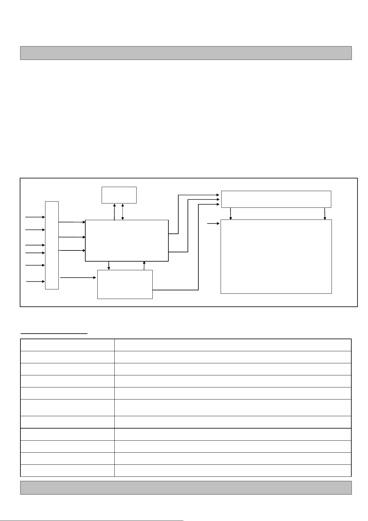
1. General Description
The LC550EQJ is a Color Active Matrix Liquid Crystal Display with an integral the Source PCB and Gate
implanted on Panel (GIP). The matrix employs a-Si Thin Film Transistor as the active element.
It is a transmissive type display operating in the normally black mode. It has a 54.64 inch diagonally measured
active display area with QWUXGA resolution (2160 vertical by 3840 horizontal pixel array).
Each pixel is divided into Red, Green and Blue sub-pixels or dots which are arranged in vertical stripes.
Gray scale or the luminance of the sub-pixel color is determined with a 10-bit gray scale signal for each dot.
Therefore, it can present a palette of more than 1.06Bilion colors.
It has been designed to apply the 10-bit 8 Lane V by One interface.
It is intended to support LCD TV, PCTV where high brightness, super wide viewing angle, high color gamut,
high color depth and fast response time are important.
EPI(RGB)
G1
Control
Signals
G2160
Data
format
Bit
select
HTPDN
LOCKN
Vby1
8lane
+12V
CN1
(51pin)
Vby1
1~8lane
Option
signal
I2C
EEPROM
SCL
SDA
Timing Controller
Vby1 Rx + DGA + ODC
Power Circuit
Block
Power Signals
General Features
Active Screen Size 54.64 inches(1387.8mm) diagonal
Outline Dimension 1225.2 (H) x 696.7 (V) x 1.4 (D) mm(Typ.)
Source Driver Circuit
S1 S3840
TFT - LCD Panel
(3840 ×RGB ×2160 pixels)
Pixel Pitch 0.315 mm x 0.315 mm
Pixel Format 3840 horiz. by 2160 vert. Pixels, RGB stripe arrangement
Color Depth 10bit(D), 1.06Billon colors
Drive IC Data Interface
Source D-IC : 8-bit EPI, gamma reference voltage, and control signals
Gate D-IC : Gate In Panel
4.84 %(Typ.)Transmittance (With POL)
Viewing angle free ( R/L 178 (Min.), U/D 178 (Min.))Viewing Angle (CR>10)
2.6(TBD)Kg (Typ.) Weight
Transmissive mode, Normally blackDisplay Mode
Hard coating(2H), Anti-glare treatment of the front polarizer 1%(Typ)Surface Treatment (Top)
Ver 0.1
3 /40
Page 5
LC550EQJ
Product Specification
2. Absolute Maximum Ratings
The following items are maximum values which, if exceeded, may cause faulty operation or permanent damage
to the LCD module.
Table 1. ABSOLUTE MAXIMUM RATINGS
Value
Parameter Symbol
Min Max
Power Input Voltage LCD Circuit VLCD -0.3 +14.0 VDC
T-Con Option Selection Voltage VLOGIC -0.3 +4.0 VDC
Unit Note
1
Operating Temperature TOP 0 +50
Storage Temperature (without packing) TST -20 +60
Panel Front Temperature TSUR - +68
C
°
C
°
C
°
Operating Ambient Humidity HOP 10 90 %RH
Storage Humidity HST 5 90 %RH
Note
1. Ambient temperature condition (Ta =
25 ± 2
°
C )
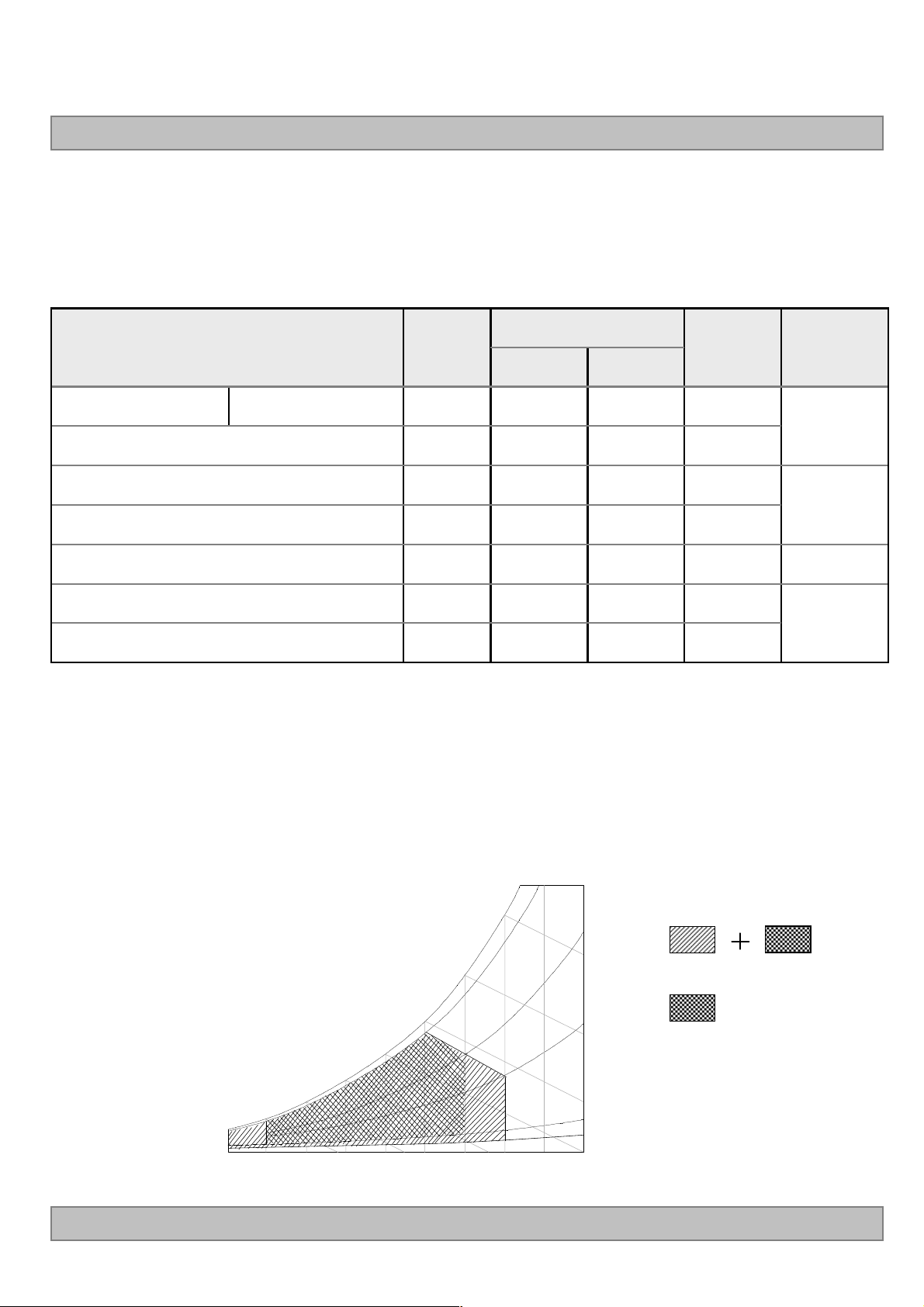
2. Temperature and relative humidity range are shown in the figure below.
Wet bulb temperature should be Max 39°C, and no condensation of water.
3. Gravity mura can be guaranteed below 40°C condition.
4. The maximum operating temperatures is based on the test condition that the surface temperature
of display area is less than or equal to 68°C with LCD module alone in a temperature controlled chamber.
Thermal management should be considered in final product design to prevent the surface temperature of
display area from being over 68℃. The range of operating temperature may be degraded in case of
improper thermal management in final product design.
90%
60
60%
2,3
4
2,3
Ver 0.1
Wet Bulb
Temperature [
10
0
10 20 30 40 50 60 70 800-20
Dry Bulb Temperature [
°
20
50
]
C
30
40
40%
Humidity [(%)RH]
10%
5%
]
C
°
Storage
Operation
4 /40
Page 6
Product Specification
3. Electrical Specifications
3-1. Electrical Characteristics
Table 2. ELECTRICAL CHARACTERISTICS
Value
Parameter Symbol
Min Typ Max
Circuit :
Power Input Voltage VLCD 10.8 12.0 13.2 VDC
Unit Note
LC550EQJ
Power Input Current ILCD
- 1450(TBD) TBD mA 1
- 2260(TBD) TBD mA 2
T-CON Option
Selection Voltage
Input High Voltage V
Input Low Voltage V
IH
IL
2.7 - 3.6 VDC
0-0.7VDC
Power Consumption PLCD - 17.4(TBD) 22.6(TBD) Watt 1
Rush current IRUSH - - TBD A 3
Note
1. The specified current and power consumption are under the V
condition, and mosaic pattern(8 x 6) is displayed and f
is the frame frequency.
V
=12.0V, Ta=25 ± 2
LCD
C, fV=60Hz
°
2. The current is specified at the maximum current pattern.
3. The duration of rush current is about 2ms and rising time of power input is 0.5ms (min.).
4. Ripple voltage level is recommended under ±5% of typical voltage
White : 1023 Gray
Black : 0 Gray
Ver 0.1
Mosaic Pattern(8 x 6)
5 /40
Page 7
LC550EQJ
Product Specification
3-2. Interface Connections
This LCD module employs one kind of interface connection, 51-pin connector is used for the module
electronics.
3-2-1. LCD Module
- LCD Connector(CN1): FI-RE51S-HF(manufactured by JAE) or GT05P-51S-H38(manufactured by LSM)
or IS050-C51B-C39(manufactured by UJU)
- Mating Connector : FI-R51HL(manufactured by JAE) or compatible
Table 3. MODULE CONNECTOR(CN2) PIN CONFIGURATION
No Symbol Description No Symbol Description
1 VLCD Power Supply +12.0V 27 GND Ground
2 VLCD Power Supply +12.0V 28 Rx0n V-by-One HS Data Lane 0
3 VLCD Power Supply +12.0V 29 Rx0p V-by-One HS Data Lane 0
4 VLCD Power Supply +12.0V 30 GND Ground
5 VLCD Power Supply +12.0V 31 Rx1n V-by-One HS Data Lane 1
6 VLCD Power Supply +12.0V 32 Rx1p V-by-One HS Data Lane 1
7 VLCD Power Supply +12.0V 33 GND Ground
8 VLCD Power Supply +12.0V 34 Rx2n V-by-One HS Data Lane 2
9 NC NO CONNECTION 35 Rx2p V-by-One HS Data Lane 2
10 GND Ground 36 GND Ground
11 GND Ground 37 Rx3n V-by-One HS Data Lane 3
12 GND Ground 38 Rx3p V-by-One HS Data Lane 3
13 GND Ground 39 GND Ground
14 NC NO CONNECTION 40 Rx4n V-by-One HS Data Lane 4
15 Data format 0
16 Data format 1 42 GND Ground
17 PCID_EN
18
19
20 NC NO CONNECTION 46 Rx6n V-by-One HS Data Lane 6
21 Bit SEL ‘H’ or NC= 10bit(D) , ‘L’ = 8bit 47 Rx6p V-by-One HS Data Lane 6
22 NC NO CONNECTION 48 GND Ground
23 AGP or NSB
24 GND Ground 50 Rx7p V-by-One HS Data Lane 7
25 HTPDN Hot plug detect 51 GND Ground
26 LOCKN Lock detect - - -
SDA SDA (For I2C)
SCL SCL (For I2C)
Input Data Format [1:0] :
‘00’=Mode1, ’01’=Mode2,
’10’=Mode3, ’11’=Mode4
‘H’ : PCID Enable
‘L’ or ‘NC’ : PCID Disable
‘H’ or NC : AGP
‘L’ : NSB (No signal Black)
41 Rx4p V-by-One HS Data Lane 4
43 Rx5n V-by-One HS Data Lane 5
44 Rx5p V-by-One HS Data Lane 5
45 GND Ground
49 Rx7n V-by-One HS Data Lane 7
Note
Ver 0.1
1. All GND (ground) pins should be connected together to the LCD module’s metal frame.
2. All Input levels of V-by-One signals are based on the V-by-One-HS Standard Version 1.4
3. #14, #20 & #22 NC(No Connection) : These pins are used only for LGD (Do not connect)
4. About specific pin(#15, #16), Please see the Appendix
Ⅷ
.
5. Specific pin No. #23 is used for “No signal detection” of system signal interface.
It should be GND for NSB (No Signal Black) while the system interface signal is not.
If this pin is “H”, LCD Module displays AGP (Auto Generation Pattern).
6 /40
Page 8
LC550EQJ
Product Specification
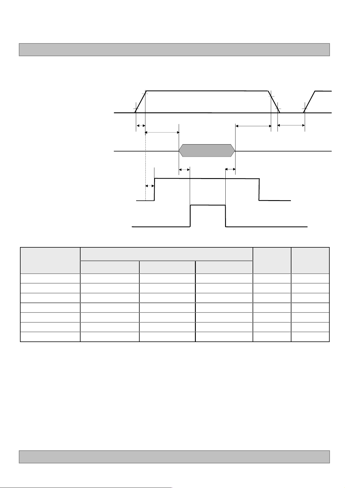
3-3. Signal Timing Specifications
Table 4 shows the signal timing required at the input of the Vx1 transmitter. All of the interface signal timings
should be satisfied with the following specification for normal operation.
Table 4. TIMING TABLE (DE Only Mode)
ITEM Symbol Min Typ Max Unit Note
Horizontal
Vertical
Frequency
Display
Period
Blank
Total
Display
Period
Blank
Total
ITEM Symbol Min Typ Max Unit Note
DCLK
Horizontal
tHV
tHB
tHP
tVV
tVB
tVP
fCLK
fH
480 480 480
50(TBD) 70 120
530(TBD) 550 600
2160 2160 2160
40 90 600
2200 2250 2760
60(TBD) 74.25 78.00
121.8
(TBD)
135 140
tCLK
tCLK
tCLK
Lines
Lines
Lines
MHz
KHz
3840/8
1
1
594/8
2
Vertical
notes: 1. The input of HSYNC & VSYNC signal does not have an effect on normal operation (DE Only Mode).
If you use spread spectrum of EMI, add some additional clock to minimum value for clock margin.
2. The performance of the electro-optical characteristics may be influenced by variance of the vertical
refresh rate and the horizontal frequency
Timing should be set based on clock frequency.
※
Ver 0.1
fV
47 60 63
Hz
2
7 /40
Page 9
Product Specification
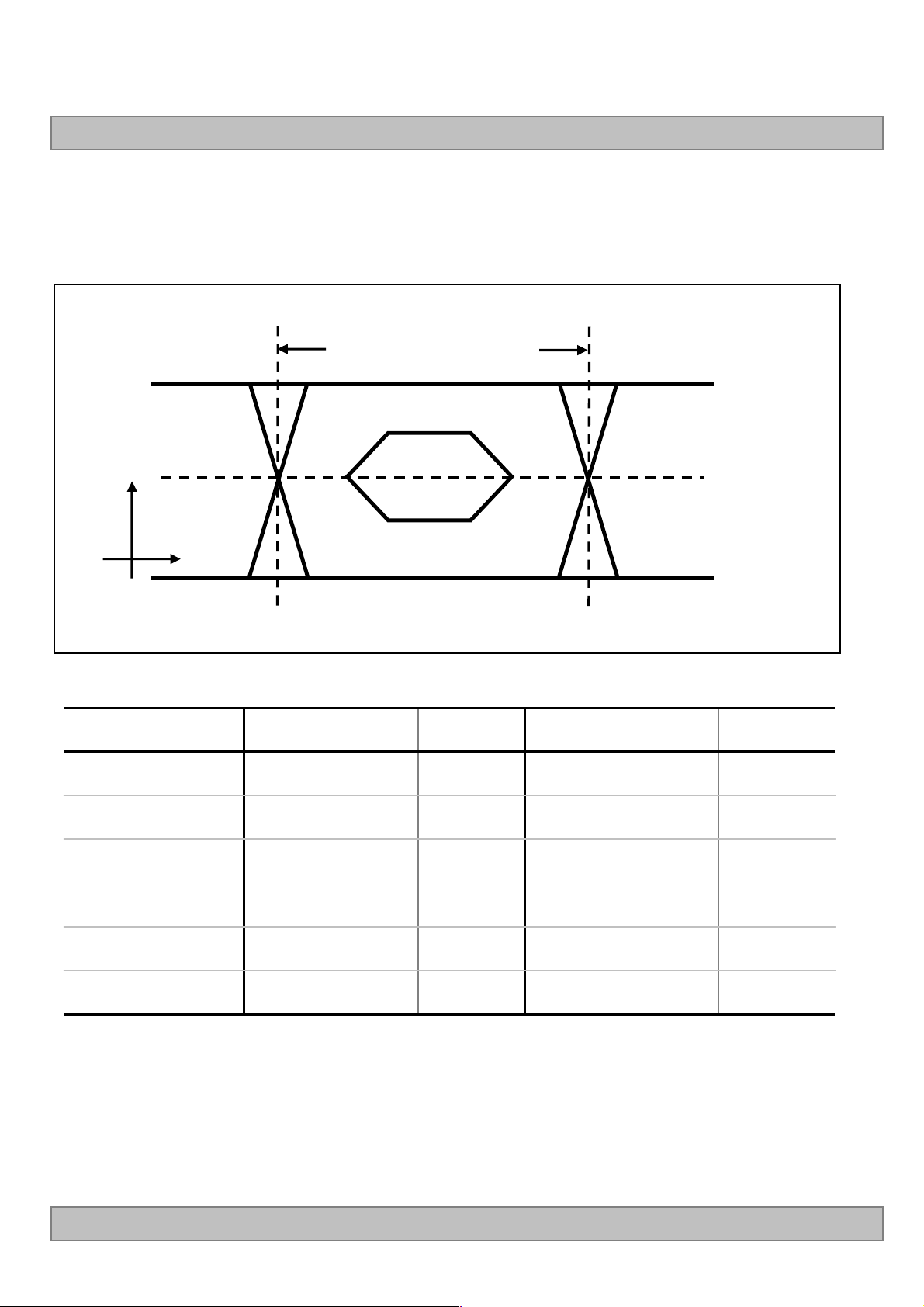
3-4. V by One input signal Characteristics
3-4-1. V by One Input Signal Timing Diagram
1UI = 1/(Serial data rate)
LC550EQJ
Y
X
X=0 UI X=1 UI
Table5. Eye Mask Specification
X[UI] Note Y[mV] Note
A 0.25 (max) 2 0 -
B 0.3 (max) 2 50 3
C 0.7(min) 3 50 3
B
ㆍ
A
ㆍ
ㆍㆍ
FE
C
ㆍ
ㆍ
D
Y=0mV
D 0.75(min) 3 0 -
E 0.7(min) 3 l -50 l 3
F 0.3(max) 2 l -50 l 3
notes 1. All Input levels of V by One signals are based on the V by One HS Standard Ver. 1.4
2. This is allowable maximum value.
3. This is allowable minimum value.
4. The eye diagram is measured by the oscilloscope and receiver CDR characteristic must be
emulated.
- PLL bandwidth : 20 Mhz(TBD)
- Damping Factor : 1.5(TBD)
Ver 0.1
8 /40
Page 10
LC550EQJ
Product Specification
3-4-2. V by One Input Signal Characteristics
1) DC Specification
VRTH
VRCT
VRTL
Description Symbol Min Max Unit
CML Differential input High threshold VRTH - 50 mV
CML common mode Bias Voltage VRCT 0.6(TBD) 0.8(TBD) V
2) AC Specification
mV--50VRTLCML Differential input Low threshold
Rx1
Rx2
Lane0
Vdiff =0
tRISK_INTER
Lane1
Vdiff =0
<Inter-pair Skew between two Lanes>
1H
T-CON
Max 1 DE
V By One Rx IP
Vblank
Hblank
DE
Rx1
(Sub Block)
Rx2
(Sub Block)
Vblank
DE
<Inter-pair Skew between two sub Blocks>
4 Lane
<TCON – VbyOne Brief Diagram >
4 Lane
Description Symbol Min Max Unit notes
Allowable inter-pair skew between lanes tRISK_INTER - 5 UI 1,3
Allowable iner-pair skew between sub-blocks tRISK_BLOCK - 1 DE 1,4
Notes 1.1UI = 1/serial data rate
2. it is the time difference between the true and complementary single-ended signals.
3. it is the time difference of the differential voltage between any two lanes in one sub block.
4. it is the time difference of the differential voltage between any two blocks in one IP.
Ver 0.1
9 /40
Page 11
3-5. Intra interface Signal Specification
3-5-1. EPI Signal Specification
Table 6. ELECTRICAL CHARACTERISTICS
Parameter Symbol Condition MIN TYP MAX Unit notes
LC550EQJ
Product Specification
Logic & EPI Power Voltage VCC - 1.62 1.8 1.98 V
DC
EPI input common voltage VCM LVDS Type 0.8 VCC/2 1.3 V
EPI input differential voltage Vdiff - 150 - 500 mV
EPI Input eye diagram Veye - 90 - - mV
Effective Veye width time B1&B2 0.25 - - UI
EPI +
0 V
Vdiff
Vdiff
(Differential Probe)
EPI -
0 V
Vdiff
Vcm
(Active Probe)
EPI Differential signal characteristics
1 UI
0.5 UI
0 V
(Differential Probe)
Ver 0.1
Veye
Veye
B1 B2
Eye Pattern of EPI Input
*Source PCB
FIG. 3 Measure point
10 /40
Page 12
LC550EQJ
Product Specification
3-6. Color Data Reference
The brightness of each primary color (red, green, blue) is based on the 10bit or 8bit gray scale data input for the color.
The higher binary input, the brighter the color. Table 8 provides a reference for color versus data input.
Table 7. COLOR DATA REFERENCE
Byte0
Byte1
Packer input &
Unpacker output
D[0] R[2] R[0]
D[1] R[3] R[1]
D[2] R[4] R[2]
D[3] R[5] R[3]
D[4] R[6] R[4]
D[5] R[7] R[5]
D[6] R[8] R[6]
D[7] R[9] R[7]
D[8] G[2] G[0]
D[9] G[3] G[1]
D[10] G[4] G[2]
D[11] G[5] G[3]
D[12] G[6] G[4]
D[13] G[7] G[5]
D[14] G[8] G[6]
D[15] G[9] G[7]
30bpp RGB (10bit) 24bpp RGB (8bit)
Byte2
Byte3
Ver 0.1
D[16] B[2] B[0]
D[17] B[3] B[1]
D[18] B[4] B[2]
D[19] B[5] B[3]
D[20] B[6] B[4]
D[21] B[7] B[5]
D[22] B[8] B[6]
D[23] B[9] B[7]
D[24] Don’t care
D[25] Don’t care
D[26] B[0]
D[27] B[1]
D[28] G[0]
D[29] G[1]
D[30] R[0]
D[31] R[1]
11 /40
Page 13
3-7. Power Sequence
3-7-1. LCD Driving circuit
LC550EQJ
Product Specification
Power Supply For LCD
V
LCD
0V
0V
Interface Signal (Tx_data)
User Control Signal
(DATA FORMAT,BIT_SEL, PCID_EN)
Power for LED
Table 8. POWER SEQUENCE
Parameter
Min Typ Max
10%
T
90%
1
T6
T2
100%
Value
Vx1 Data
T3 T4
LED ON
90%
10%
T
7
Unit Notes
10%
T5
Note :
1 0.5 - 20 ms 1
T
2 0--ms2
T
3 400 - - ms 3
T
4 100 --ms3
T
5 1.0 - - s 4
T
6 0-T2ms5
T
T7
1. Even though T1 is over the specified value, there is no problem if I2T spec of fuse is satisfied.
2. If T2 is satisfied with specification after removing V by One Cable, there is no problem.
3. The T3 / T4 is recommended value, the case when failed to meet a minimum specification,
abnormal display would be shown. There is no reliability problem.
4. T5 should be measured after the Module has been fully discharged between power off and on period.
5. If the on time of signals (Interface signal and user control signals) precedes the on time of Power (V
it will be happened abnormal display. When T6 is NC status, T6 doesn’t need to be measured.
6. It is recommendation specification that T7 has to be 0ms as a minimum value.
Please avoid floating state of interface signal at invalid period.
※
When the power supply for LCD (VLCD) is off, be sure to pull down the valid and invalid data to 0V.
※
There is no problem even though LOCKN/HTPDN Signal is on before T1.
※
LCD
6ms--0
),
Ver 0.1
12 /40
Page 14

LC550EQJ
Product Specification
4. Optical Specification
Optical characteristics are determined after the unit has been ‘ON’ and stable in a dark environment at 25±2°C.
The values are specified at distance 50cm from the LCD surface at a viewing angle of and equal to 0 °.
FIG. 1 shows additional information concerning the measurement equipment and method.
Optical Stage(x,y)
LCD Module
Pritchard 880 or
equivalent
50cm
FIG. 1 Optical Characteristic Measurement Equipment and Method
Ta= 25
Table 9. OPTICAL CHARACTERISTICS
±2°
C
, V
=12.0V, fV=60Hz, Dclk=74.25MHz
LCD
EXTVbr-B=100%
Value
Parameter Symbol
Unit notes
Min Typ Max
Contrast Ratio CR 1000(TBD) 1400(TBD) - 1
Response Time
Color Coordinates
[CIE1931]
Viewing
Angle
2D
(CR>10)
Variation G to G
σ
Gray to Gray (BW) G to G BW 8(TBD) 12(TBD)
RED
GREEN
BLUE
right(=0°) r (x axis)
left (=180°) l (x axis)
up (=90°) u (y axis)
down (=270°) d (y axis)
Rx
Ry TBD
Gx TBD
Gy TBD
Bx TBD
By TBD
Typ
-0.03
89 - -
89 - -
89 - -
89 - -
6 9
ms
TBD
Typ
+0.03
degree 4
3
2
3D
(CT≤10%)
Gray Scale - - - 5
up + down
Ver 0.1
u (y axis)
+d (y axis)
11(TBD) - - degree 6
13 /40
Page 15

Product Specification
Note : 1. Contrast Ratio(CR) is defined mathematically as :
CR(Contrast Ratio) = Maximum CRn (n=1, 2, 3, 4, 5)
Surface Luminance at position n with all white pixels
CRn =
Surface Luminance at position n with all black pixels
n = the Position number(1, 2, 3, 4, 5). For more information, see FIG 2.
LC550EQJ
2. Response time is the time required for the display to transit from any gray to white (Rise Time, Tr
and from any gray to black (Decay time, Tr
※
G to G
Spec stands for average value of all measured points.
BW
Photo Detector : RD-80S / Field : 2
3. G to G
is Variation of Gray to Gray response time composing a picture
σ
(Xi- u)
Σ
G to G (σ) =
√
4. Viewing angle is the angle at which the contrast ratio is greater than 10. The angles are
determined for the horizontal or x axis and the vertical or y axis with respect to the z axis which
is normal to the LCD module surface. For more information, see the FIG. 4.
5. Gray scale specification
Gamma Value is approximately 2.2. For more information, see the Table 10.
6. 3D performance specification is expressed by 3D luminance and 3D viewing angle.
Table 10. GRAY SCALE SPECIFICATION
)
). For additional information see the FIG. 3.
D
R
°
2
N
Xi = Individual Data
u = Data average
N : The number of Data
Ver 0.1
Gray Level Luminance [%] (Typ)
L0 0.07(TBD)
L63
L127
L191
L255
L319
L383
L447
L511
L575
L639
L703
L767
L831
L895
L959
L1023
0.27
1.04
2.49
4.68
7.66
11.5
16.1
21.6
28.1
35.4
43.7
53.0
63.2
74.5
86.7
100
14 /40
Page 16

Measuring point for Contrast Ratio
LC550EQJ
Product Specification
H
A
③②
V
①
B
A : H / 4 mm
④
FIG. 2 Points for Contrast Ratio Measure
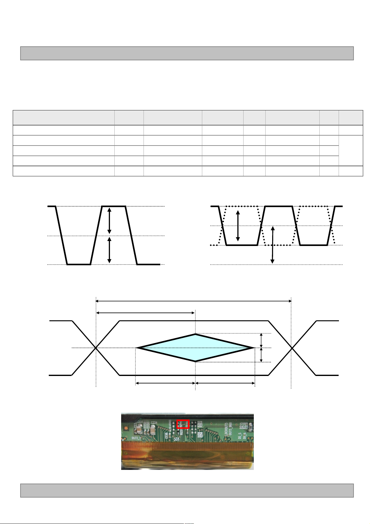
Response time is defined as the following figure and shall be measured by switching the input signal for
“Gray(N)” and “Black or White”.
Tr
100
90
⑤
Tf
B : V / 4 mm
@ H,V : Active Area
Ver 0.1
Optical
Response
10
0
Gray(N)
White
N = 0(Black)~1023(White)
FIG. 3 Response Time
Gray(N)
Black
15 /40
Page 17

imension of viewing angle range
D
= 180°, Left
Product Specification
Normal
E
Y
= 90°, Up
= 0°, Right
LC550EQJ
= 270°, Down
FIG. 4 Viewing Angle
Ver 0.1
16 /40
Page 18

Product Specification
LC550EQJ
LW-RW
LB-RW
LW-RB
LB-RB
(a) Test pattern image
2
6
45
7
1
9
3
8
3D display
(b) Measurement
position
< FIG.5 Measurement configuration>
Luminance
Lum( LE or RE, test pattern, number )
Measurement through
Left or Right eyeglass
LMS
Right or left eyeglass
( Circular polarizer )
(c) Setup
measurement
position
< FIG.6 Positioning eyeglass >
< FIG. 7 notation of luminance measurement >
In order to measure 3D luminance, 3D crosstalk and 3D viewing angle, it need to be prepared as below;
1) Measurement configuration
4-Test pattern images. Refer to FIG 5.
-. LW-RW : White for left and right eye
-. LW-RB : White for left eye and Black for right eye
-. LB-RW : Black for left eye and white for right eye
-. LB-RB : Black for left eye and right eye
Image files where black and white lines are displayed on even or odd lines.
Luminance measurement system (LMS) with narrow FOV (field of view) is used. Refer to FIG 1.
2) Positioning Eyeglass (refer to appendix-V for standard specification of eyeglass)
Find angle of minimum transmittance.
This value would be provided beforehand or measured by the following steps;
(i) Test image (LB-RW) is displayed.
(ii) Left eyeglass are placed in front of LMS and luminance is measured,
rotating right eyeglass such as FIG 6. The notation for luminance measurement is “Lum(LE, LB-RW,1)”.
(iii) Find the angle where luminance is minimum.
* Following measurements should be performed at the angle of minimum transmittance of eyeglass.
Ver 0.1
17 /40
Page 19

Product Specification
3) Measurement of 3D luminance
(i) Test image ( LW-RW ) is displayed.
(ii) Left or right eyeglass are placed in front of LMS successively and
luminance is measured at center 1 point where the notation for luminance measurement is
“Lum(LE, LW-RW,1)” or “Lum(RE, LW-RW,1).
4) Measurement of 3D crosstalk
(i) Test image ( LB-RW, LW-RB and LB-RB ) is displayed.
(ii) Right or left eyeglass are placed in front of LMS successively and
luminance is measured for position 1.
with rotating LMS or sample vertically.
Lum(LE, LB-RW,1) - Lum(LE, LB-RB,1)
Lum(LE, LW-RB,1) - Lum(LE, LB-RB,1)
or
Lum(RE, LW-RB,1) - Lum(RE, LB-RB,1)
Lum(RE, LB-RW,1) - Lum(RE, LB-RB,1)
LC550EQJ
5) Measurement of 3D Viewing Angle
3D viewing angle is the angle at which the 3D crosstalk is under 10%. The angles are
determined for the vertical or y axis with respect to the z axis which is normal to the LCD
module surface and measured for position 1. For more information , see the Fig 8
S
M
L
z axis
L
M
S
LW-RB LB-RW
LCM
y axis
yu(up)
Φ
yd (down)
Φ
LB-RB
LMS
Ver 0.1
(a) Test pattern image
(b) Measurement of 3D viewing angle (up/down)
< FIG.8 Measurement of 3D crosstalk and 3D viewing angle >
18 /40
Page 20
Product Specification
5. Mechanical Characteristics
Table 11 provides general mechanical characteristics.
Table 11. MECHANICAL CHARACTERISTICS
Item Value
Horizontal 1225.2 mm
Outline Dimension
(Only Glass)
Active Display Area
Vertical 696.7 mm
Depth 1.4 mm
Horizontal 1209.6 mm
Vertical 680.4 mm
LC550EQJ
Weight
Surface Treatment
2.6(TBD)Kg (Typ.)
Hard coating(2H),
Anti-glare treatment of the front polarizer : Haze 1%(typ.)
Note : Please refer to a mechanic drawing in terms of tolerance at the next page.
Ver 0.1
19 /40
Page 21

6. Mechanical Dimension
6-1. Board Assembly Dimension
Product Specification
y
r
a
n
i
m
i
l
e
r
P
LC550EQJ
Ver 0.1
20 /40
Page 22

Product Specification
6-2. Control Board Assembly Dimension
P
r
e
l
m
i
i
n
a
r
LC550EQJ
y
Ver 0.1
21 /40
Page 23

Product Specification
7. Reliability
Table 12. ENVIRONMENT TEST CONDITION
No. Test Item Condition
1 High temperature storage test Ta= 60°C 90% 240h
2 Low temperature storage test Ta= -20°C 240h
3 High temperature operation test Ta= 50°C 50%RH 500h
4 Low temperature operation test Ta= 0°C 500h
5 Humidity condition Operation Ta= 40 °C ,90%RH
LC550EQJ
6
Altitude operating
storage / shipment
0 - 16,400 ft
0 - 40,000 ft
Note : Before and after Reliability test, LCM should be operated with normal function.
Ver 0.1
22 /40
Page 24

Product Specification
8. International Standards
8-1. Safety
a) UL 60065, Underwriters Laboratories Inc.
Audio, Video and Similar Electronic Apparatus - Safety Requirements.
b) CAN/CSA C22.2 No.60065:03, Canadian Standards Association.
Audio, Video and Similar Electronic Apparatus - Safety Requirements.
c) IEC 60065, The International Electrotechnical Commission (IEC).
Audio, Video and Similar Electronic Apparatus - Safety Requirements.
8-2. Environment
a) RoHS, Directive 2011/65/EU of the European Parliament and of the council of 8 June 2011
LC550EQJ
Ver 0.1
23 /40
Page 25

Product Specification
9. Packing
9-1. Packing Form
a) Package quantity in one Pallet : 70 pcs
b) Pallet Size : 1390 mm(W) X 890 mm(D) X 980 mm(H)
LC550EQJ
Ver 0.1
24 /40
Page 26

LC550EQJ
Product Specification
10. Precautions
Please pay attention to the followings when you use this TFT LCD module.
10-1. Handling Precautions
(1) Please attach the surface transparent protective film to the surface in order to protect the polarizer.
Transparent protective plate should have sufficient strength in order to the resist external force.
(2) Acetic acid type and chlorine type materials for the cover case are not desirable because the former
generates corrosive gas of attacking the polarizer at high temperature and the latter causes circuit break
by electro-chemical reaction.
(3) Do not touch, push or rub the exposed polarizers with glass, tweezers or anything harder than HB
pencil lead. And please do not rub with dust clothes with chemical treatment.
Do not touch the surface of polarizer for bare hand or greasy cloth.(Some cosmetics are detrimental
to the polarizer.)
(4) After removing the protective film, when the surface becomes dusty, please wipe gently with absorbent
cotton or other soft materials like chamois soaks with petroleum benzine.
Do not use acetone, toluene and alcohol because they cause chemical damage to the polarizer.
(5) Wipe off saliva or water drops as soon as possible. Their long time contact with polarizer causes
deformations and color fading.
(6) Since a module is composed of electronic circuits, it is not strong to electrostatic discharge.
Make certain that treatment persons are connected to ground through wrist band etc. And don’t touch
interface pin directly. Panel ground path should be connected to metal ground.
(7) Please make sure to avoid external forces applied to the Source PCB and D-IC during the process of
handling or assembling the TV set. If not, It causes panel damage or malfunction.
(8) Panel and BLU should be protected from the static electricity. If not, it causes IC damage.
(9) Do not pull or fold the source D-IC which connect the source PCB and the panel.
(10) Panel(board ass’y) should be put on the BLU structure precisely to avoid mechanical impact.
(11) FFC Cable should be connected between System board and Source PCB correctly.
(12) Mechanical structure for backlight system should be designed for sustaining board ass’y safely.
(13) Surface temperature of the Source D-IC should be controlled under 100℃with TV Set status.
If not, problems such as IC damage or decrease of lifetime could occur.
10-2. Operating Precautions
(1) Response time depends on the temperature.(In lower temperature, it becomes longer.)
(2) Brightness depends on the temperature. (In lower temperature, it becomes lower.)
And in lower temperature, Stable time(required time that brightness is stable after turned on)
becomes longer
(3) Be careful for condensation at sudden temperature change. Condensation makes damage to polarizer or
electrical contacted parts. And after fading condensation, smear or spot will occur.
(4) When fixed patterns are displayed for a long time, remnant image is likely to occur.
(5) Module has high frequency circuits. Sufficient suppression to the electromagnetic interference shall be
done by system manufacturers. Grounding and shielding methods may be important to minimized the
interference.
Ver 0.1
25 /40
Page 27

Product Specification
10-3. Protection Film
(1) Please keep attaching the protection film before assembly.
(2) Please peel off the protection film slowly.
(3) Please peel off the protection film just like shown in the Fig.1
(4) Ionized air should be blown over during the peeling.
(5) Source PCB should be connected to the ground when peel off the protection film.
(6) The protection film should not be contacted to the source D-IC during peeling it off.
10-4. Storage Precautions
When storing modules as spares for a long time, the following precautions are necessary.
p
e
e
l
i
n
LC550EQJ
g
d
i
r
e
c
t
i
o
n
< Fig. 1 >
(1) Temperature : 5 ~ 40
℃
(2) Humidity : 35 ~ 75 %RH
(3) Period : 6 months
(4) Control of ventilation and temperature is necessary.
(5) Please make sure to protect the product from strong light exposure, water or moisture. Be careful for
condensation.
(6) Please keep the modules at a circumstance shown below Fig. 2
No Baking 50℃, 10%, 24hr 50℃, 10%, 48hr
2 month
3 month
6 month
< Fig. 2 >
10-5. Packing Precautions
Product assembled into module should be stored in the Al-bag(cover case).
10-6. Operating condition guide
(1) The LCD product should be operated under normal conditions. Normal condition is defined as below;
- Temperature : 5 ~ 40 ℃, normal humidity
- Display pattern : continually changing pattern (Not stationary)
(2) If the product will be used in extreme conditions such as high temperature, display patterns or operation
time etc..,
It is strongly recommended to contact LGD for Qualification engineering advice. Otherwise, its reliability
and function may not be guaranteed. Extreme conditions are commonly found at Airports, Transit Stations,
Banks, Stock market, and Controlling systems. The LCD product should be applied by global standard
environment. (refer ETSI EN 300, IEC 60721)
Ver 0.1
26 /40
Page 28

# APPENDIX-Ⅰ-1
Pallet Ass’y
■
①
LC550EQJ
Product Specification
ⓑ
②
ⓐ
③
Desiccant X4
⑤
Ⓙ
ⓒ
ⓓ
ⓔ
④
No. Description Material
ⓐ
Pallet Plywood
⑥
Ver 0.1
ⓑ
ⓒ
ⓓ
ⓔ
ⓕ
ⓖ
ⓗ
ⓘ
Ⓙ
Carton Plate Single Wall
PE Sheet Carbon
Top Packing EPS
Bottom Packing EPS
Angle Packing Single Wall
Tape OPP
Band PP
Clip Steel
Desiccant Power dry
27 /40
Page 29

Product Specification
# APPENDIX-Ⅰ-2
Control PCB Packing Ass’y
■
a) Control PCB Qty / Box : 70 pcs
b) Tray Qty / Box : 13Tray(Upperst Tray Is empty)
c) Tray Size : 353 X 353 X 16 (TBD)
d) Box size : 368 X 355 X 98 (TBD)
[10pcs/Tray]
LC550EQJ
[7Tray+Empty Tray]
[7Tray]
[Inserting into Box]
NO. DESCRIPTION MATERIAL
1 PCB Packing A,ssy -
2 Tray PET
Ver 0.1
3Box SWR4
28 /40
Page 30

# APPENDIX-Ⅱ-1
LC550EQJ
Product Specification
20±0.2mm
6±0.2mm
LC550EQJ-SGK1
Model Name
Serial Label
Ver 0.1
29 /40
Page 31

# APPENDIX-Ⅱ-2
BOX Label
■
LC550EQJ
Product Specification
LC550EQJ-SGK1
QTY : 10
Pallet Label
■
LC550EQJ
SGK1
70 PCS
MADE IN KOREA
001/01-01
XXXXXXXXXXXXX XXX
RoHS Verified
Ver 0.1
30 /40
Page 32

Product Specification
LC550EQJ
# APPENDIX-
Required signal assignment for Flat Link (Thine : THCV216) Transmitter
■
Ⅲ
TX’s Inner Structure
Packer Scrambler 8/10b Encoder Serializer
8
8
8
8
D[31:24]
D[23:16]
D[15:8]
D[7:0]
PD[7:0]
8
PD[7:0]
H
G
F
E
D
C
B
A
D/K
H
G
F
E
D
C
B
A
D/K
Timing diagram of the Serializer
First
abcde i f ghg
j
h
g
f
i
e
d
c
b
a
j
h
g
f
i
e
d
c
b
a
Tx_n
Tx_p
Last
time
THCV216
FI-RE51(41)S-HF
or Compatible
100nF
8
D[31:24]
8
D[23:16]
Tx’s
8
D[15:8]
Inner
Strucure
Tx_n
100nF
Tx_p
HTPDN
Timing
Controller
Rx_n
Rx_p
HTPDN
8
D[7:0]
LOCKN
LOCKN
VCC
notes: 1. The LCD module uses a 100 nF capacitor on positive and negative lines of each receiver input.
2. Refer to Vx1 Transmitter Data Sheet for detail descriptions. (THCV216 or Compatible)
3. About Module connector pin configuration, Please refer to the Page 7.
Ver 0.1
31 /40
Page 33

Product Specification
# APPENDIX-Ⅳ-1
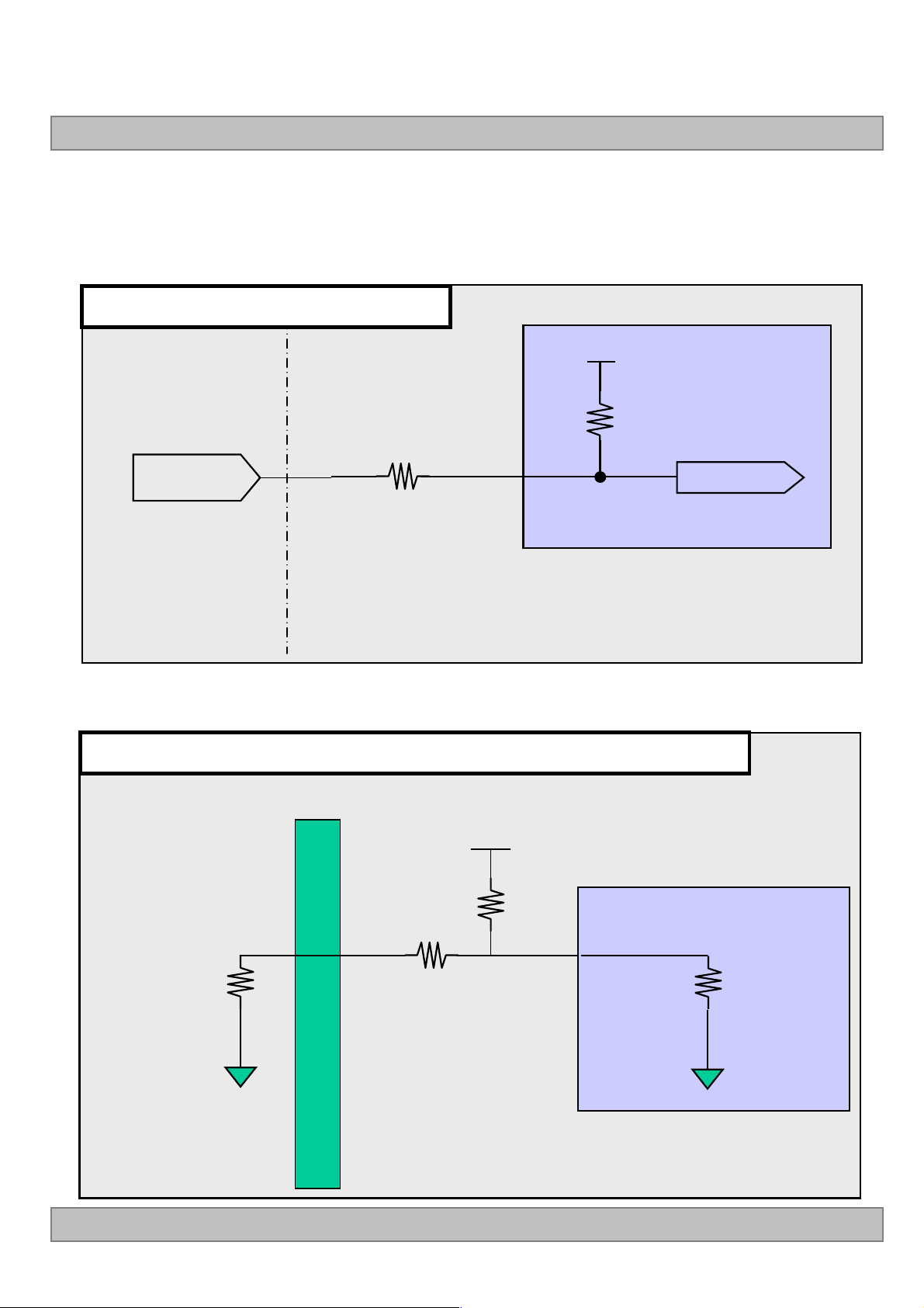
Option Pin Circuit Block Diagram
■
1) Circuit Block Diagram of Data format Selection pin
Data format Select Pin : Pin 15, Pin16
1K
Data format Select
(Pin 15,16)
LC550EQJ
Ω
Data format Select
System Side LCM Side
2) Circuit Block Diagram of PCID Enable pin
PCID Enable Pin : Pin 17
1K
PCID_EN
(Pin 17)
Ω
60k
Ω
(TBD)
ASIC
(TCON)
PCID_EN
Ver 0.1
60k
Ω
(TBD)
System Side LCM Side
ASIC
(TCON)
32 /40
Page 34
# APPENDIX-Ⅳ-2
Option Pin Circuit Block Diagram
■
3) Circuit Block Diagram of Bit Selection pin
Bit Select Pin : Pin 21
Bit Select
(Pin 21)
Product Specification
65k
1K
Ω
(TBD)
LC550EQJ
VCC
Ω
Bit Select
ASIC
(TCON)
System Side LCM Side
4) Circuit Block Diagram of AGP Selection pin
AGP(auto Generation Pattern ) or NSB (no signal black) : Pin 23
FI-RE51S-HF
Vcc : 3.3V
10k
Ω
R1
≤
(0
recommand)
Ω
1k
pin
#23
Ω
1k
Ω
60k
Ω
(TBD)
ASIC
(TCON)
Ver 0.1
System Side
LCM Side
33 /40
Page 35

# APPENDIX-Ⅳ-3
Option Pin Circuit Block Diagram
■
5) I2C (SDA/SCL) Selection Pin
SDA/SCL : Pin 18, 19
LC550EQJ
Product Specification
SDA/SCL
(Pin 18, 19)
100
Ω
4.7k
Ω
(TBD)
VCC
ASIC
(TCON)
EEPROM
Slave Address : 70
EEPROM
Slave Address : A0
PM IC
Slave Address : 40
System Side LCM Side
Note : I2C Line of Set Soc avoid using slave address 40, 70, A0 because LCD module uses those
Ver 0.1
34 /40
Page 36

Product Specification
LC550EQJ
# APPENDIX-
Standard specification of Eyeglasses
■
Ⅴ
This is recommended data of Eyeglasses for LC550EQJ-SGK1 model. (details refer to table 13)
For each item, depending on the eyeglass manufacturer tolerances may occur, this tolerance can
affect 3D performance. (3D Crosstalk, 3D luminance, 3D viewing angle)
<Table 13. Standard specification of Eyeglasses>
Design item of Eyeglasses Left Right Remark
Optical
axis
a) Slow axis of retarder
b) Transmission axis of polarizer
Retardation
value
Recommended polarizer
※
Retarder 125nm @550nm
-45
0
˚
˚
45
0
˚
˚
Refer to
drawing
Polarization efficiency: more than 99.90%
Bottom
Bottom
POL
POL
90
90˚90
˚
Top
Top
POL
POL
˚
Patterned
Patterned
0
0˚0
˚
˚
Cell Patterned
Cell Patterned
-45
retarder
retarder
retarder
retarder
45
45
45
45
135
135
135
135
45˚45
Retarder
Retarder
Polarizer
Polarizer
+λ/4
˚
˚
˚
˚
˚
˚
˚
˚
˚
˚
-λ/4
-λ/4
+λ/4
Left eye
Left eyeLeft eye
Right eye
Right eyeRight eye
Direction from viewer
a) Slow axis of retarder
a) Slow axis of retarder
-45
-45
˚
˚
Left Right
Left Right
45
45
b) Transmission axis of polarizer
b) Transmission axis of polarizer
˚
˚
0
0
˚
˚
Left Right
Left Right
0
0
˚
˚
Ver 0.1
(b) Configuration of Eyeglasses
<Drawing. Information of optical axis>
35 /40
Page 37

Product Specification
LC550EQJ
# APPENDIX-
Flicker Adjustment
■
Parameter Unit Min Typ Max Note
Inversion Method - V2-Dot Inversion
Adjust Pattern /
Gray Level
Position - Center
Voltage range V 4.84(TBD) 5.39(TBD) 5.95(TBD)
Ⅵ
- V2Dot Full Flicker / 511Gray 60Hz
R G
Row 1
Row 1
Row 2
Row 2
R G
B
B
R G
R G
B
B
R G
R G
B
B
R G
R G
B
B
511Gray
SCL
SDA
Adjustment JIG
A
Row 3
Row 3
Row 4
Row 4
B
PMIC
LCD Module
0Gray
A : Pull-up Resistors
(If it is necessary)
B : I2C Connector
(Refer to Appendix IX)
Ver 0.1
36 /40
Page 38

Product Specification
LC550EQJ
# APPENDIX-
The reference method of BL dimming
■
It is recommended to use synchronous V-sync frequency to prevent waterfall
(Vsync * 2 =P-Dim Frequency)
Ⅶ
Ver 0.1
37 /40
Page 39

# APPENDIX-Ⅷ-1
input mode of pixel data
■
LC550EQJ
Product Specification
Mode 2 : 2 DivisionMode 1 : Non-Division
Lane 1stData 2
nd
Data Data#
Lane0 1 9 3833
Lane1 2 10 3834
Lane2 3 11 3835
Lane3 4 12 3836
Lane4 5 13 3837
Lane5 6 14 3838
Lane6 7 15 3839
Lane7 8 16 3840
Lane 1stData 2
nd
Data Data#
Lane0 1 5 1917
Lane1 2 6 1918
Lane2 3 7 1919
Lane3 4 8 1920
Lane4 1921 1925 3837
Lane5 1922 1926 3838
Lane6 1923 1927 3839
Lane7 1924 1928 3840
Ver 0.1
38 /40
Page 40

# APPENDIX-Ⅷ-2
input mode of pixel data
■
LC550EQJ
Product Specification
Mode 4 : 8 DivisionMode 3 : 4 Division
Lane 1stData 2
nd
Data Data#
Lane0 1 3 959
Lane1 2 4 960
Lane2 961 963 1919
Lane3 962 964 1920
Lane4 1921 1923 2879
Lane5 1922 1924 2880
Lane6 2881 2883 3839
Lane7 2882 2884 3840
Lane 1stData 2
nd
Data Data#
Lane0 1 2 480
Lane1 481 482 960
Lane2 961 962 1440
Lane3 1441 1442 1920
Lane4 1921 1922 2400
Lane5 2401 2402 2880
Lane6 2881 2882 3360
Lane7 3361 3362 3840
Ver 0.1
39 /40
Page 41

Product Specification
# 0.31+0.03/
-
0.02
# 0.31+0.03/
-
0.02
LC550EQJ
# APPENDIX-
1.0 ±1.0
±
Ⅸ
Adhesive
Area
Silicone Tape
Area
Adhesive
Area
e
r
P
Adhesive - left Adhesive - right
Adhesive - left Adhesive - right
Conductor Pad
Conductor Pad
m
i
l
(Stiffener)
16.0+0.8/-0.4
(Adhesive)
(Adhesive)
4.5+0.8/-0.4
4.5+0.8/-0.4
Bottom Side
Bottom Side
n
i
a
y
r
(Adhesive)
(Adhesive)
4.5+0.8/-0.4
4.5+0.8/-0.4
# 0.5 +0.07/-0.045
# 0.5 +0.07/-0.045
# 3+0.5/-0.35
# 3+0.5/-0.35
◈
< Pad Detail– 68Pin >
< Pad Detail– 68Pin >
# 34.5 +0.06/-0.035
# 34.5 +0.06/-0.035
## 0.5±0.05
## 0.5±0.05
# 33.5±0.05
# 33.5±0.05
Note
- Pad : GOLD Plating
-
-## ≥Cpk 1.33
- Stiffener color : Sky Blue
#≥
Cpk 1.0
# 0.3 mm Max
# 0.3 mm Max
# 0.3+0.04/-0.02
# 0.3+0.04/-0.02
# 0.31+0.03/-0.02
# 0.31+0.03/-0.02
- Material List
Ver 0.1
-H-F
- Dimensions unit : mm
40 /40
 Loading...