

Page 1
LC470DUS
Product Specification
SPECIFICATION
FOR
APPROVAL
Preliminary Specification
)
(
●
)
(
Final Specification
Title
BUYER AmTRAN
MODEL
APPROVED BY
/
/
SIGNATURE
DATE
47.0” WUXGA TFT LCD
SUPPLIER LG.Display Co., Ltd.
*MODEL LC470DUS
SUFFIX SCM1 (RoHS Verified)
*When you obtain standard approval,
please use the above model name without
suffix
APPROVED BY
P.Y. Kim / Team Leader
REVIEWED BY
Y. J. Heo / Project Leader
SIGNATURE
DATE
/
Please return 1 copy for your confirmation with
your signature and comments.
Ver. 1.1
PREPARED BY
O.S. Yoo / Engineer
TV Products Development Dept.
LG. Display LCD Co., Ltd
0 /340 /34
Page 2
Product Specification
CONTENTS
LC470DUS
Number ITEM
COVER 1
CONTENTS
RECORD OF REVISIONS
1 GENERAL DESCRIPTION
2 ABSOLUTE MAXIMUM RATINGS
3 ELECTRICAL SPECIFICATIONS
3-1 ELECTRICAL CHARACTERISTICS
3-2 INTERFACE CONNECTIONS
3-3 SIGNAL TIMING SPECIFICATIONS
3-4 DATA MAPPING AND TIMING
3-5 PANEL PIXEL STRUCTURE
3-6 POWER SEQUENCE
4 OPTICAL SPECIFICATIONS
5 MECHANICAL CHARACTERISTICS
Page
2
3
4
5
6
6
9
12
15
16
17
18
22
6RELIABILITY
7 INTERNATIONAL STANDARDS
7-1 SAFETY
7-2 Environment
8PACKING
8-1 DESIGNATION OF LOT MARK
8-2 PACKING FORM
9PRECAUTIONS
9-1 MOUNTING PRECAUTIONS
9-2 OPERATING PRECAUTIONS
9-3 ELECTROSTATIC DISCHARGE CONTROL
9-4 PRECAUTIONS FOR STRONG LIGHT EXPOSURE
9-5 STORAGE
9-6 HANDLING PRECAUTIONS FOR PROTECTION FILM
Ver. 1.1
25
26
26
26
27
27
27
28
28
28
29
29
29
29
1 /341 /34
Page 3
Product Specification
RECORD OF REVISIONS
Revision No. Revision Date Page Description
0.1 May, 25, 2010 - Preliminary Specification (First Draft)
LC470DUS
Ver. 1.1
2 /342 /34
Page 4
LC470DUS
Product Specification
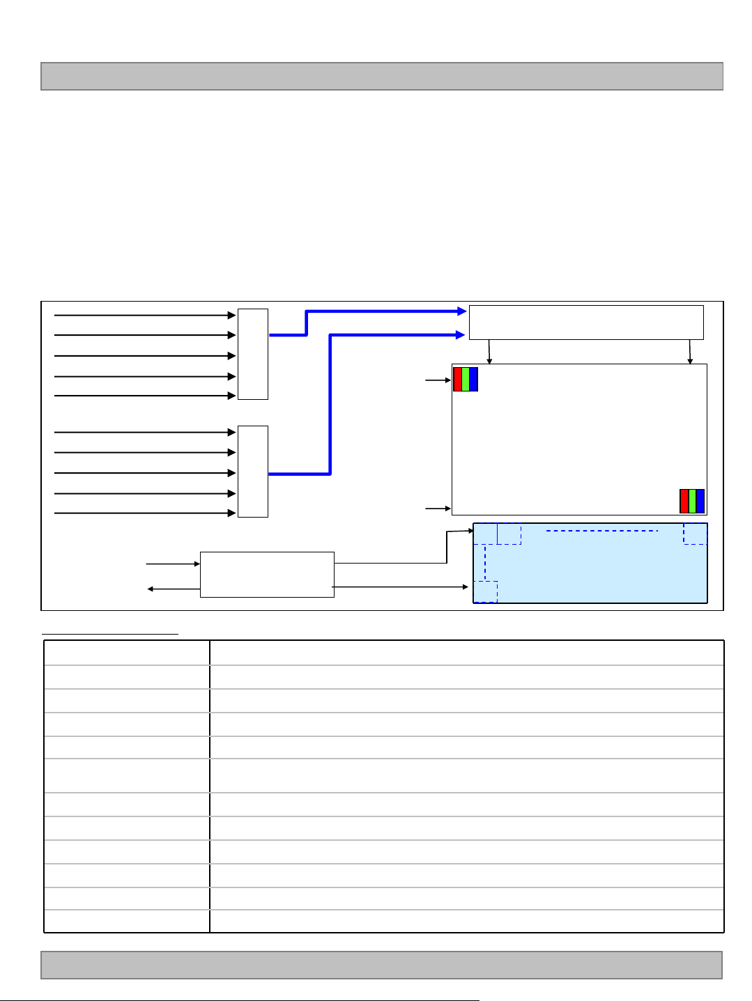
1. General Description
The LC470DUS is a Color Active Matrix Liquid Crystal Display with an integral Light Emitting Diode (LED)
Local Dimming backlight system. The matrix employs a-Si Thin Film Transistor as the active element.
It is a transmissive type display operating in the normally black mode. It has a 46.96 inch diagonally measured
active display area with WUXGA resolution (1080 vertical by 1920 horizontal pixel ar
Each pixel is divided into Red, Green and Blue sub-pixels or dots which are arranged in vertical stripes.
Gray scale or the luminance of the sub-pi xel color is determined with a 10-bit gray scale signal for each dot.
Therefore, it can present a palette of more than 1.06B(FRC) colors.
It is intended to support LCD TV, PCTV where high brightness, super wide viewing angle, high color gamut,
high color depth and fast response time are important.
Power (VCC, VDD, VGH, VGL)
Source Control Signal
Gate Control Signal
Gamma Reference Voltage
mini-LVDS (RGB) for Left drive
CN1
(80pin)
S1 S1920
G1
Source Driver Circuit
ray).
Power (VCC, VDD, VGH, VGL)
Source Control Signal
Gate Control Signal
Gamma Reference Voltage
mini-LVDS (RGB) for Right drive
LED Anode
LED Cathode
CN2
(80pin)
CN1 (100Pin)
CN2 (100pin)
G1080
TFT - LCD Panel
(1920 × RGB × 1080 pixels)
[Gate In Panel]
Local Dimming : 160 Block
H : 10Block
General Features
Active Screen Size 46.96 inches(1192.87mm) diagonal
Outline Dimension 1096.0(H) x 640.0 (V) x 35.5 mm(D) (Typ.)
Pixel Pitch 0.5415 mm x 0.5415 mm
Pixel Format 1920 horiz. by 1080 vert. Pixels, RGB stripe arrangement
Color Depth 8-bit, 16.7M colors ( ※ 1.06B colors @10bit (D) System Output )
Drive IC Data Interface
Luminance, White 500 cd/m2 (Center 1point ,Typ.)
Source D-IC : 8-bit mini-LVDS, gamma reference voltage, and control signals
Gate D-IC : Line on Glass(LOG) Through Source D-IC
V : 16Block
Viewing Angle (CR>10) Viewing angle free ( R/L 178 (Min.), U/D 178 (Min.))
Power Consumption Total TBDW (Typ.) (Logic=8.76 W, LED Backlight =TBDW)
Weight 13Kg (Typ.)
Display Mode Transmissive mode, Normally black
Surface Treatment Hard coating(3H), Anti-reflection treatment of the front polarizer (Reflectance : 2%)
Ver. 1.1
3 /343 /34
Page 5
LC470DUS
Product Specification
2. Absolute Maximum Ratings
The following items are maximum values wh ich, if exceeded, may cause faulty operation or damage to the
LCD module.
Table 1. ABSOLUTE MAXIMUM RATINGS
Parameter Symbol
Logic Power Voltage VCC -0.5 +4.0 VDC
Gate High Voltage VGH +18.0 +30.0 VDC
Gate Low Voltage VGL -8.0 -4.0 VDC
Source D-IC Analog Voltage VDD -0.3 +18.0 VDC
Gamma Ref. Voltage (Upper) VGMH
Gamma Ref. Voltage (Low) VGML -0.3
LED Input Voltage VF - 13.6 VDC
Panel Front Temperature TSUR - +68 °C 4
Operating Temperature TOP 0 +50 °C
Storage Temperature TST -20 +60 °C
Operating Ambient Humidity HOP 10 90 %RH
Storage Humidity HST 10 90 %RH
Note:
1. Ambient temperature condition (Ta = 25 ± 2 °C )
Min Max
½VDD-0.5
Value
VDD+0.5 VDC
½ VDD+0.5
Unit Note
VDC
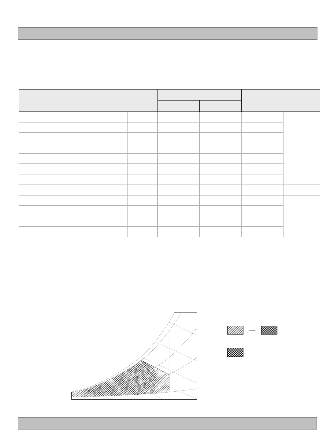
2. Temperature and relative humidity range are shown in the figure below. Wet bulb temperature
should be Max 39 °C and no condensation of water.
3. Gravity mura can be guaranteed below 40℃ condition.
4. The maximum operating temperature is based on the test condition that the surface temperature
of display area is less than or equal to 68 ℃ with LCD module alone in a temperature controlled
chamber. Thermal management should be considered in final product design to prevent the surface
temperature of display area from being over 68 ℃. The range of operating temperature may
degrade in case of improper thermal management in final product design.
90%
60
60%
1
2,3
Ver. 1.1
Wet Bulb
Temperature [
10
0
10 20 30 40 50 60 70 800-20
Dry Bulb Temperature [
°C]
20
30
40
50
°C]
40%
10%
Humidity
[(%)RH]
Storage
Operation
4 /344 /34
Page 6
LC470DUS
Product Specification
3. Electrical Specifications
3-1. Electrical Characteristics
It requires several power inputs. The VCC is the basic power of LCD Driving power sequence, Which is used
to logic power voltage of Source D-IC and GIP.
Table 2. ELECTRICAL CHARACTERISTICS
Parameter Symbol Condition MIN TYP MAX Unit Note
Logic Power Voltage VCC - 3.0 3.3 3.6
Logic High Level Input Voltage VIH 2.3 VCC VDC
Logic Low Level Input Voltage VIL 00.8VDC
Source D-IC Analog Voltage VDD - 16.3 16.5 16.7 VDC
Half Source D-IC Analog
Voltage
Gamma Reference Voltage
Common Voltage Vcom - 5.9 6.2 6.5 V
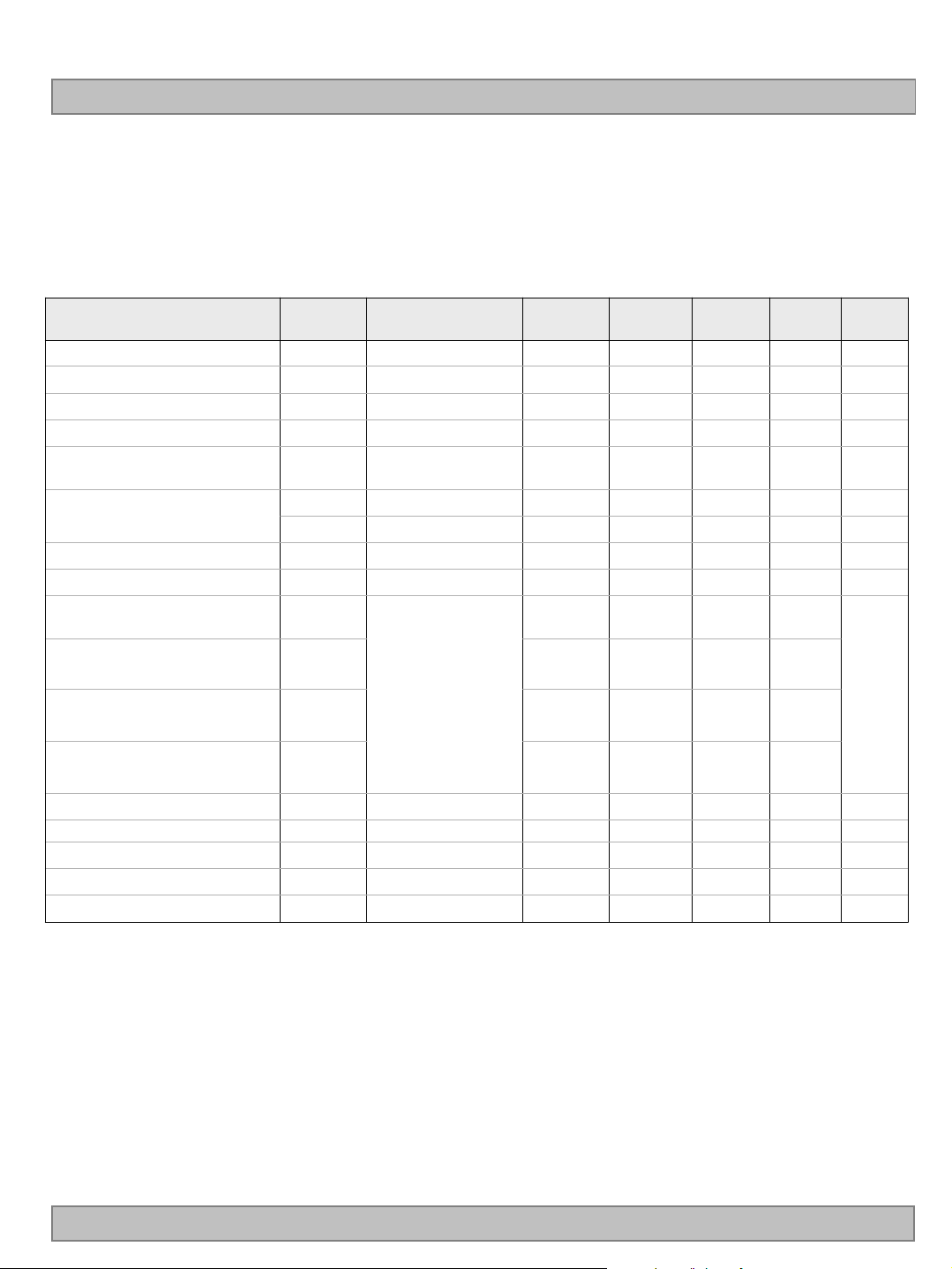
Mini-LVDS Clock frequency CLK 3.0V≤VCC ≤3.6V 312 MHz
mini-LVDS input Voltage
(Center)
mini-LVDS input Voltage
Distortion (Center)
mini-LVDS differential
Voltage range
mini-LVDS differential
Voltage range Dip
Gate High Voltage VGH 26.7 27.0 27.3 VDC
Gate Low Voltage VGL -5.2 -5.0 -4.8 VDC
Gate High Modulation Voltage VGHM - - 19 - VDC Fig.1
Total Power Current
Total Power Consumption
H_VDD - 8.05 8.25 8.45 VDC
V
GMH
V
GML
V
IB
ΔV
IB 0.8 V
VID 150 800 mV
ΔVID
ILCD - - 1010 1315 mA 1,2
PLCD - - 12.1 15.8 Watt
(GMA1 ~ GMA9) ½*VDD VDD-0.2
(GMA10 ~ GMA18) 0.2 ½*VDD
0.7 +
(VID/2)
Mini-LVDS Clock
and Data
25 800 mV
(VCC-1.2)
−VID / 2
VDC
V
5
1. The specified current and power consumption are under the V
Note:
condition whereas mosaic pattern(8 x 6) is displayed and f
2. The above spec is based on the basic model.
3. All of the typical gate voltage should be controlled within 1% voltage level
4. Ripple voltage level is recommended under 10%
5. In case of mini-LVDS signal spec, refer to Fig 2 for the more detail.
Ver. 1.1
LCD=12V., 25 ± 2°C, f
is the frame frequency.
V
= 240Hz
V
5 /345 /34
Page 7
VCM (0V)
LC470DUS
Product Specification
VGH
VGHM
GND
VGL
Without GPM With GPM
FIG. 1 Gate Output Wave form without GPM and with GPM
VID
△VID
△VIB
VIB
VID
* Differential Probe
△VID
* Active Probe
FIG. 2 Description of VID, ΔVIB, ΔVID
* S ource P C B
FIG. 3 Measure point
Ver. 1.1
6 /346 /34
Page 8
Product Specification
Table 3. ELECTRICAL CHARACTERISTICS (Continue)
LC470DUS
Parameter Symbol
Backlight Assembly :
Forward Current
(one array)
Forward Voltage V
Forward Voltage Variation △V
Power Consumption P
Burst Dimming Duty On duty TBD TBD %
Burst Dimming Frequency 1/T TBD TBD Hz 8
LED Array : (APPENDIX-V)
Life Time 30,000 Hrs 7
Notes :
The design of the LED driver must have specifications for the LED array in LCD Assembly.
Anode I
Cathode I
F (anode)
F (cathode)
F
F
BL
Min Typ Max
TBD
12.0 12.8 13.6 Vdc 4
TBD TBD TBD W 6
Values
TBD mAdc
95mA[TBD]
TBD mAdc
1.2 Vdc 5
Unit Note
The electrical characteristics of LED driver are based on Constant Current driving type.
The performance of the LED in LCM, for example life time or brightness, is extremely influenced by the
characteristics of the LED Driver. So, all the parameters of an LED driver should be carefully designed.
When you design or order the LED driver, please make sure unwanted lighting caused by the mismatch of the
LED and the driver (no lighting, flicker, etc) has never been occurred. When you confirm it, the LCD–
Assembly should be operated in the same condition as installed in your instrument.
1. Electrical characteristics are based on LED Array specification.
2. Specified values are defined for a Backlight Assembly. (IBL : 10 LED array, 880mA/LED array)
3. Each LED array has 2 anode terminals and 16 cathode terminals.
The forward current(I
) of 2 anode terminals is 880mA and it supplies 55mA into 16 blocks, respectively
F
4 (LED Pakage / 1string)
±5%
2, 3
Anode
4. The forward voltage(V
5. ΔV
means Max VF-Min VFin one Backlight. So VFvariation in a Backlight isn’t over Max. 1.2V
F
°°°
°°°
°°°
°°°
) of LED array depends on ambient temperature (Appendix-V)
F
Cathode #1
Cathode #2
16 (LED String / 1 Array)
Cathode #16
6. Maximum level of power consumption is measured at initial turn on.
Typical level of power consumption is measured after 1hrs aging at 25 ± 2°C.
7. The life time(MTTF) is determined as the time at which brightness of the LED is 50% compared to that of
initial value at the typical LED current on condition of continuous operating at 25 ± 2°C, based on duty 100%.
8. The reference method of burst dimming duty ratio.
It is recommended to use synchronous V-sync frequency to prevent waterfall
(Vsync x 1 =Burst Frequency)
Though PWM frequency is over 182Hz (max252Hz), function of backlight is not affected.
Ver. 1.1
7 /347 /34
Page 9
LC470DUS
Product Specification
3-2. Interface Connections
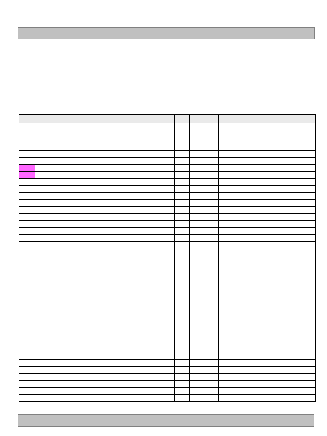
This LCD module employs two kinds of interface connection, two 80-pin FFC connector are used for the
module electronics and two 100-pin FFC connectors are used for the integral backlight system.
3-2-1. LCD Module
-LCD Connector (CN1): TF06L-80S-0.5SH (Manufactured by Hirose) or Equivalent
Table 4-1. MODULE CONNECTOR(CN1) PIN CONFIGURATION
No Symbol Description No Symbol Description
1 VDD Driver Power Supply Voltage 41 GND Ground
2 VDD Driver Power Supply Voltage 42 POL Polarity Output Signal
3 GND Ground 43 GSP Gate Start Pulse
4 VCC Logic Power Supply Voltage 44 H_CONV Horizontal 2 Inversion Signal
“H”
5 VCC Logic Power Supply Voltage 45 OPT_N
6 GND Ground 46 GND Ground
7 HVDD Half Driver Power Supply Voltage 47 LRV5 - Left Right Mini LVDS Receiver Signal(5-)
8 HVDD Half Driver Power Supply voltage 48 LRV5 + Left Right Mini LVDS Receiver Signal(5+)
9 GND Ground 49 LRV4 - Left Right Mini LVDS Receiver Signal(4-)
10 VGL Gate Low Voltage 50 LRV4 + Left Right Mini LVDS Receiver Signal(4+)
11 GND Ground 51 LRV3 - Left Right Mini LVDS Receiver Signal(3-)
12 GOE Gate Output Enable 52 LRV3 + Left Right Mini LVDS Receiver Signal(3+)
13 GSC Gate Shift Clock 53 GND Ground
14 GND Ground 54 LRVCLK - Left Right Mini LVDS Receiver Clock(-)
15 VGH Gate High Voltage 55 LRVCLK + Left Right Mini LVDS Receiver Clock(+)
16 GND Ground 56 GND Ground
17 LVCOM_FB Vcom Feedback 57 LRV2 - Left Right Mini LVDS Receiver Signal(2-)
18 VCOM_L Left Vcom Output 58 LRV2 + Left Right Mini LVDS Receiver Signal(2+)
19 GND Ground 59 LRV1 - Left Right Mini LVDS Receiver Signal(1-)
20 ZOUT LTD Output 60 LRV1 + Left Right Mini LVDS Receiver Signal(1+)
21 GND Ground 61 LRV0 - Left Right Mini LVDS Receiver Signal(0-)
22 GND Ground 62 LRV0 + Left Right Mini LVDS Receiver Signal(0+)
23 GMA18 Gamma Voltage 18 63 GND Ground
24 GMA17 Gamma Voltage 17 64 LLV5 - Left Left Mini LVDS Receiver Signal(5-)
25 GMA16 Gamma Voltage 16 65 LLV5 + Left Left Mini LVDS Receiver Signal(5+)
26 GMA15 Gamma Voltage 15 66 LLV4 - Left Left Mini LVDS Receiver Signal(4-)
27 GMA14 Gamma Voltage 14 67 LLV4 + Left Left Mini LVDS Receiver Signal(4+)
28 GMA13 Gamma Voltage 13 68 LLV3 - Left Left Mini LVDS Receiver Signal(3-)
29 GMA12 Gamma Voltage 12 69 LLV3 + Left Left Mini LVDS Receiver Signal(3+)
30 GMA10 Gamma Voltage 10 70 GND Ground
31 GMA9 Gamma Voltage 9 71 LLVCLK - Left Left Mini LVDS Receiver Clock(-)
32 GMA7 Gamma Voltage 7 72 LLVCLK + Left Left Mini LVDS Receiver Clock(+)
33 GMA6 Gamma Voltage 6 73 GND Ground
34 GMA5 Gamma Voltage 5 74 LLV2 - Left Left Mini LVDS Receiver Signal(2-)
35 GMA4 Gamma Voltage 4 75 LLV2 + Left Left Mini LVDS Receiver Signal(2+)
36 GMA3 Gamma Voltage 3 76 LLV1 - Left Left Mini LVDS Receiver Signal(1-)
37 GMA2 Gamma Voltage 2 77 LLV1 + Left Left Mini LVDS Receiver Signal(1+)
38 GMA1 Gamma Voltage 1 78 LLV0 - Left Left Mini LVDS Receiver Signal(0-)
39 GND Ground 79 LLV0 + Left Left Mini LVDS Receiver Signal(0+)
40 SOE Source Output Enable 80 GND Ground
Normal Display / “L”Rotation Display
Note :
Ver. 1.1
1. Please refer to application note (Half VDD & Gamma Voltage setting) for details.
8 /348 /34
Page 10
Product Specification
-LCD Connector (CN2): TF06L-80S-0.5SH (Manufactured by Hirose) or Equivalent
Table 4-2. MODULE CONNECTOR(CN2) PIN CONFIGURATION
No Symbol Description No Symbol Description
1 GND Ground 41 GSP Gate Start Pulse
2 RRV5 - Right Right Mini LVDS Receiver Signal(5-) 42 GND Ground
3 RRV5 + Right Right Mini LVDS Receiver Signal(5+) 43 GMA 18 Gamma Voltage 18
4 RRV4 - Right Right Mini LVDS Receiver Signal(4-) 44 GMA 17 Gamma Voltage 17
5 RRV4 + Right Right Mini LVDS Receiver Signal(4+) 45 GMA 16 Gamma Voltage 16
6 RRV3 - Right Right Mini LVDS Receiver Signal(3-) 46 GMA 15 Gamma Voltage 15
7 RRV3 + Right Right Mini LVDS Receiver Signal(3+) 47 GMA 14 Gamma Voltage 14
8 GND Ground 48 GMA 13 Gamma Voltage 13
9 RRVCLK - Right Right Mini LVDS Receiver Clock(-) 49 GMA 12 Gamma Voltage 12
10 RRVCLK + Right Right Mini LVDS Receiver Clock(+) 50 GMA 10 Gamma Voltage 10
11 GND Ground 51 GMA 9 Gamma Voltage 9
12 RRV2 - Right Right Mini LVDS Receiver Signal(2-) 52 GMA 7 Gamma Voltage 7
13 RRV2 + Right Right Mini LVDS Receiver Signal(2+) 53 GMA 6 Gamma Voltage 6
14 RRV1 - Right Right Mini LVDS Receiver Signal(1-) 54 GMA 5 Gamma Voltage 5
15 RRV1 + Right Right Mini LVDS Receiver Signal(1+) 55 GMA 4 Gamma Voltage 4
16 RRV0 - Right Right Mini LVDS Receiver Signal(0-) 56 GMA 3 Gamma Voltage 3
17 RRV0 + Right Right Mini LVDS Receiver Signal(0+) 57 GMA 2 Gamma Voltage 2
18 GND Ground 58 GMA 1 Gamma Voltage 1
19 RLV5 - Right Left Mini LVDS Receiver Signal(5-) 59 GND Ground
20 RLV5 + Right Left Mini LVDS Receiver Signal(5+) 60 ZOUT LTD Output
–
21
22 RLV4 + Right Left Mini LVDS Receiver Signal(4+) 62 VCOM_R Right Vcom Output
23 RLV3 - Right Left Mini LVDS Receiver Signal(3-) 63 RVCOM_FB NC(TBD)
24 RLV3 + Right Left Mini LVDS Receiver Signal(3+) 64 GND Ground
25 GND Ground 65 VGH Gate High Voltage
26 RLVCLK - Right Left Mini LVDS Receiver Clock(-) 66 GND Ground
27 RLVCLK + Right Left Mini LVDS Receiver Clock(+) 67 GSC Gate Shift Clock
28 GND Ground 68 GOE Gate Output Enable
29 RLV2 - Right Left Mini LVDS Receiver Signal(2-) 69 GND Ground
30 RLV2 + Right Left Mini LVDS Receiver Signal(2+) 70 VGL Gate Low Voltage
31 RLV1 - Right Left Mini LVDS Receiver Signal(1-) 71 OPT_P
32 RLV1 + Right Left Mini LVDS Receiver Signal(1+) 72 GND Ground
33 RLV0 - Right Left Mini LVDS Receiver Signal(0-)
34 RLV0 + Right Left Mini LVDS Receiver Signal(0+)
35 GND Ground 75 GND Ground
36 OPT_N
37 H_CONV Horizontal 2 Inversion Signal 77 VCC Logic Power Supply Voltage
38 SOE Source Output Enable 78 GND Ground
39 GND Ground 79 VDD Driver Power Supply Voltage
40 POL Polarity Output Signal 80 VDD Driver Power Supply Voltage
RLV4
Right Left Mini LVDS Receiver Signal(4-) 61 GND Ground
“L”
Normal Display / “H”Rotation Display
73 HVDD Half Driver Power Supply Voltage
74 HVDD Half Driver Power Supply voltage
“H”
Normal Display / “L”Rotation Display
76 VCC Logic Power Supply Voltage
LC470DUS
Note :
1. Please refer to application note (Half VDD & Gamma Voltage setting) for details.
Source Right PCB
Ver. 1.1
CN 2
#1 #80
CN 1
Source Left PCB
#1 #80
9/349/34
Page 11
3-2-2. Backlight Module
LC470DUS
Product Specification
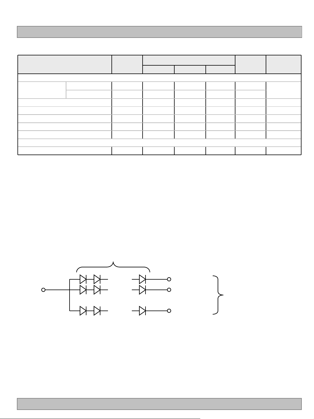
[ CN1 ]
1) LED Array assy Connector (Receptacle)
: 05002HR-100G3 (manufactured by Yeonho) or equivalent
[ CN2 ]
1) LED Array assy Connector (Receptacle)
: 05002HR-100G3 (manufactured by Yeonho) or equivalent
Table 5. BACKLIGHT CONNECTOR PIN CONFIGURATION(CN1,CN2)
No Symbol
1~9
#1 Anode
10
11~90
Cathode
91
92~10
0
#2 Anode
N.C
N.C
Description
LED Input Current
Open
LED Output
Current
Open
LED Input Current
Note
Appendix-
V
No Symbol
1~9
#3 Anode
10
11~90
Cathode
91
92~10
0
#4 Anode
◆ Rear view of LCM
100
99
98
1
2
3
N.C
N.C
Description
LED Input Current
Open
LED Output
Current
Open
LED Input Current
Note
Appendix-
V
Ver. 1.1
.
.
.
3
2
1
[ CN1 ]
98
99
100
[ CN2 ]
.
.
.
10 /3410 /34
Page 12

3-3. Signal Timing Specifications
Table 6. Timing Requirements
Parameter Symbol Condition Min Typ Max Unit Note
LC470DUS
Product Specification
Mini Clock pulse period
Mini Clock pulse low period
Mini Clock pulse high period
Mini Data setup time
Mini Data hold time
Reset low to SOE rising time
SOE to Reset input time
Receiver off to SOE timing
POL signal to SOE setup time
POL signal to SOE hold time
Reset High Period
SOE signal GSP setup time
SOE signal GSP Hold time
SOE signal Pulse Width
Note :
Note :
1. Mini-LVDS timing measure conditions
: 268MHz < Clock Frequency < 312MHz , 150mV < VID < 800mV @
2. Setup time and hold time couldn’t be satisfied at the same time
T1
T2
T3
T6
T7
T8
T9
T10
T11
T12
T13
T14
T15
T16
3.2 3.4 ns
1.6 - - ns
1.6 - - ns
0.6 - - ns
0.6 - - ns
0--ns
200 - - ns
10 - -
-5 - - ns
6--ns
3
100 ns
100 ns
200 ns
CLK
cycle
CLK
cycle
3.0<VCC<3.3
1
Ver. 1.1
CLK-
CLK+
LV0+, -
to
LV5+,-
T1
70%
T7
T2
T5
70%
30%
T5
30%
30%
30%
T4
70%
T4
T6 T7
50%
T3
T6
FIG 4. Source D-IC Input Data Latch Timing Waveform
70%
VDIFF
VDIFF
11 /3411 /34
Page 13

Product Specification
LC470DUS
CLK+
LV0+,LV1+,-
to
LV5+,-
SOE
Read The Reset=H
Read The Reset=L 1
T1
T2
T3
NA
R=H R=H R=H NAR=L R=L NA D D DR=L DD
T13
NA
T8
70%
30%
NA NA NA NANA NA NA D D DNA DD
T9
FIG 5-1. Input Data Timing for 1stSource D-IC Chip
Last DATA
st
DATA
Ver. 1.1
CLK+
LV0+,-
LV1+,-
to
LV5+,-
SOE
(640) (641)
D D D
D D D
FIG 5-2. Last Data Latch to SOE Timing
NA NA NA NA NA R=LNA R=L R=L
NA NA NA NA NA NANA NA NA
T10
T8
70%
30%
12 /3412 /34
Page 14

Product Specification
LC470DUS
SOE
POL
GSP
GSP
70%
T16
T14
T11
70%
30%
30%
70%
T15
T12
70%
30%
70%
30%
70%
Ver. 1.1
SOE
1stline data 1stline output
FIG 6. POL, GSP and SOE Timing Waveform
13 /3413 /34
Page 15

Product Specification
3-4. Data Mapping and Timing
Display data and control signal (RESET) are input to LV0 to LV5.
3-4-1. Control signal input mode
CLK +
LC470DUS
LV0 +
RESET RESET RESET RESET RESET RESET RESET RESET RESET RESET
3-4-2. Display data input mode
CLK+
LV0+
LV1+
LV2+
LV3+
LV4+
LV5+
Note :
1. For data mapping, please refer to panel pixel structure Fig.8
D01 D02 D03 D04 D05 D06D00
D11 D12 D13 D14 D15 D16D10 D17
D21 D22 D23 D24 D25 D26D20 D27
D31 D32 D33 D34 D35 D36D30 D37
D41 D42 D43 D44 D45 D46D40 D47
D51 D52 D53 D54 D55 D56D50 D57
DATA INPUT CYCLE
D07 D00
Fig. 7 Mini-LVDS Data
D10
D20
D30
D40
D50
Ver. 1.1
14 /3414 /34
Page 16

3-5. Panel Pixel Structure
D1 D2 D3 D4 D5 D1918 D1919 D1920 D1921
G1
G2
G3
G4
G5
G6
LC470DUS
Product Specification
G1078
G1079
G1080
FIG. 8 Panel Pixel Structure
Ver. 1.1
15 /3415 /34
Page 17

3-6. Power Sequence
3-6-1. LCD Driving circuit3-6-1. LCD Driving circuit
LC470DUS
Product Specification
Power Supply For LCD VCC
Power Supply For LCD
VDD, HVDD, VGH,
Gamma Ref. Voltage
Power Supply For LCD
VGL
GSC and GOE Signal
Power for Lamp
0V
0V
GSC
GOE
70%
50%
T1
T4
T2
VGH=Vcc
100%
Don’t care
T7
50% 50%
......
......
..
T3
T5
Lamp ON
T5’
50%
30%
30%
T6
Table 7. POWER SEQUENCE
Parameter
T
1 0.5 - ms
2 0.01
T
T
3 20(1~2frame)
T
4 0T2ms
5 / T5’
T
T
6 2-sec
7 0.5 - s
T
20(1~2frame) - ms
Value
Min Typ Max
Ta= 25±2°C, fV=240Hz, Dclk=297MHz
Unit Notes
-
-
ms
ms
Note : 1. Power sequence for Source D-IC must be kept. ※ Please refer to Appendix IV for more details
2. The Gate D-IC power on sequence must be VCC, VGL, logic input & VGH.
4. The 1
st
start of GSC is located between VGL and VGH.
5. GOE rising is before GSC.
6. Power off sequence order is reverse of power on sequence.
Ver. 1.1
16 /3416 /34
Page 18

LC470DUS
Product Specification
4. Optical Specification
Optical characteristics are determined after the unit has been ‘ON’ and stable in a dark environment at
25±2°C. The values are specified at an approximate distance 50cm from the LCD surface at a viewing angle
of Φ and θ equal to 0 °.
It is presented additional information concerning the measurement equipment and method in FIG. 9.
Optical Stage(x,y)
LCD Module
Pritchard 880 or
equivalent
50cm
FIG. 9 Optical Characteristic Measurement Equipment and Method
Ta= 25±2°C, V
=12.0V, fV=240Hz, Dclk=297MHz,
LCD
Table 8. OPTICAL CHARACTERISTICS
Parameter Symbol
Contrast Ratio CR 900 1300 - 1
Surface Luminance, white L
Luminance Variation
Rising Tr -
Response Time
Falling Tf -
RED
Color Coordinates
[CIE1931]
Color Temperature 10,000 K
Color Gamut 72 %
Viewing Angle (CR>10)
x axis, right(φ=0°) θr
x axis, left (φ=180°) θl
y axis, up (φ=90°) θu
y axis, down
(φ=270°)
Gray Scale - - - 6
GREEN
BLUE
WHITE
WH
δ
WHITE
5P - - 1.3 3
Rx 0.652(TBD)
Ry 0.330(TBD)
Gx 0.305(TBD)
Gy 0.597(TBD)
Bx 0.149(TBD)
By 0.060(TBD)
Wx 0.279(TBD)
Wy 0.292(TBD)
θd
Min Typ Max
400 500 - cd/m
Typ
-0.03
89 - 89 - 89 - -
89 - -
Value
4(TBD)
4(TBD)
Unit Note
2
ms 4
Typ
+0.03
degree 5
2
Ver. 1.1
17 /3417 /34
Page 19

Product Specification
Note :
1. Contrast Ratio(CR) is defined mathematically as :
CR =
It is measured at center 1-point
2. Surface luminance is determined after the unit has been ‘ON’ and 1Hour after lighting the
backlight in a dark environment at 25±2°C. Surface luminance is the luminance value at center
1-point across the LCD surface 50cm from the surface with all pixels displaying white.
For more information see the FIG. 10.
3. The variation in surface l umin ance , δ WHITE is defined as :
δ WHITE(5P) = Maximum(L
Where L
For more information, see the FIG. 10.
4. Response time is the time required for the display to transit from G(255) to G(0) (Rise Time, Tr
and from G(0) to G(255) (Decay Time, Tr
5. Viewing angle is the angle at which the contrast ratio is greater than 10. The angles are
determined for the horizontal or x axis and the vertical or y axis with respect to the z axis which
is normal to the LCD module surface. For more information, see the FIG. 12.
Surface Luminance at all white pixels
Surface Luminanc e at all bl ack pix els
on1,Lon2
on1
to L
are the luminance with all pixels displaying white at 5 locations .
on5
, L
on3
LC470DUS
, L
, L
on4
).
D
) / Minimum(L
on5
on1,Lon2
, L
on3
, L
on4
, L
on5
)
)
R
6. Gray scale specification
Gamma Value is approximately 2.2. For more information, see the Table 9.
Table 9. GRAY SCALE SPECIFICATION
Gray Level Luminance [%] (Typ)
L0 0.07
L15 0.24
L31 1.04
L47 2.49
L63 4.68
L79 7.66
L95 11.5
L111 16.1
L127 21.6
L143 28.1
L159 35.4
L175 43.7
L191 53.0
L207 63.2
L223 74.5
L239 86.7
L255 100
Positive
Voltage
Negative
Voltage
Gray Level Gamma Ref.
L0 Gamma9
L1 Gamma8
L31 Gamma7
L63 Gamma6
L127 Gamma5
L191 Gamma4
L223 Gamma3
L255 Gamma1
L255 Gamma18
L223 Gamma16
L191 Gamma15
L127 Gamma14
L63 Gamma13
L31 Gamma12
L1 Gamma11
L0 Gamma10
Ver. 1.1
18 /34
18 /34
Page 20

Product Specification
Measuring point for surface luminance & luminance variation
H
A
LC470DUS
③②
V
①
B
A : H / 4 mm
④
FIG. 10 5 Points for Luminance Measure
Response time is defined as the following figure and shall be measured by switching the input signal for
“Gray(N)” and “Gray(M)”.
TrR
100
90
⑤
TrD
B : V / 4 mm
@ H,V : Active Area
Ver. 1.1
Optical
Response
10
0
Gray(N)
N,M = Black~White, N<M
FIG. 11 Response Time
Gray(M)
Gray(N)
19 /3419 /34
Page 21

Dimension of viewing angle range
LC470DUS
Product Specification
φ
= 180°, Left
φ
= 270°, Down
Normal
θ
φ
FIG.12 Viewing Angle
E
Y
φ
= 90°, Up
φ
= 0°, Right
Ver. 1.1
20 /3420 /34
Page 22

Product Specification
5. Mechanical Characteristics
Table 10 provides general mechanical characteristics.
Table 10. MECHANICAL CHARACTE RISTIC S
Item Value
Horizontal 1096.0 mm
LC470DUS
Outline Dimension
Bezel Area
Active Display Area
Weight 13 Kg (Typ.) , 14Kg (Max.)
Vertical 640.0 mm
Depth 35.5 mm
Horizontal 1049.0 mm
Vertical 593.0 mm
Horizontal 1039.68 mm
Vertical 584.82 mm
Note : Please refer to a mechanical drawing in terms of tolerance at the next page.
Ver. 1.1
21 /3421 /34
Page 23

[ FRONT VIEW ]
LC470DUS
Product Specification
Ver. 1.1
22 /3422 /34
Page 24

[ REAR VIEW ]
LC470DUS
Product Specification
Ver. 1.1
23 /3423 /34
Page 25

Product Specification
6. Reliability
Table 11. ENVIRONMENT TEST CONDITION
No. Test Item Condition
1 High temperature storage test Ta= 60°C 240h
2 Low temperature storage test Ta= -20°C 240h
3 High temperature operation test Ta= 50°C 50%RH 240h
4 Low temperature operation test Ta= 0°C 240h
Wave form : random
Vibration test
5
(non-operating)
Shock test
6
(non-operating)
Vibration level : 1.0Grms
Bandwidth : 10-300Hz
Duration : X,Y,Z, 30 min
Each direction per 10 min
Shock level : 50Grms
Waveform : half sine wave, 11ms
Direction : ±X, ±Y, ±Z
One time each direction
LC470DUS
7 Humidity condition Operation Ta= 40 °C ,90%RH
Altitude operating
8
storage / shipment
0 - 15,000 ft
0 - 40,000 ft
Note : Before and after Reliability test, LCM should be operated with normal function.
Ver. 1.1
24 /3424 /34
Page 26

Product Specification
7. International Standards
7-1. Safety
a) UL 60065, Seventh Edition, Underwriters Laboratories Inc.
Audio, Video and Similar Electronic Apparatus - Safety Requirements.
b) CAN/CSA C22.2 No.60065:03, Canadian Standards Association.
Audio, Video and Similar Electronic Apparatus - Safety Requirements.
c) EN 60065:2002 + A11:2008, European Committee for Electrotechnical Standardization (CENELEC).
Audio, Video and Similar Electronic Apparatus - Safety Requirements.
d) IEC 60065:2005 + A1:2005, The International Electrotechnical Commission (IEC).
Audio, Video and Similar Electronic Apparatus - Safety Requirements.
(Including report of IEC60825-1:2001 clause 8 and clause 9)
Notes
1. Laser (LED Backlight) Informati on
Class 1M LED Product
IEC60825-1 : 2001
Embedded LED Power (Class1M)
Power : 1.8163 mW (Max.)
Wavelength : 279 ~605 (nm)
Width : 0.6 x 0.6 (mm)
LC470DUS
2. Caution
: LED inside.
Class 1M laser (LEDs) radiation when open.
Do not open while operating.
7-2. Environment
a) RoHS, Directive 2002/95/EC of the European Parliament and of the council of 27 January 2003 on the
restriction of the use of certain hazardous substances in electrical and electronic equipment
Ver. 1.1
25 /3425 /34
Page 27

8. Packing
8-1. Information of LCM Label
a) Lot Mark
ABCDEFGHI JKLM
A,B,C : SIZE(INCH) D : YEAR
E : MONTH F ~ M : SERIAL NO.
Note
1. YEAR
Year
Product Specification
200320022001
200452005
2006720078200892009
LC470DUS
2010
Mark
321
4
6
2. MONTH
Month
Mark
Apr5May
4
Jun7Jul8Aug9Sep
6
b) Location of Lot Mark
Serial NO. is printed on the label. The label is attached to the backside of the LCD module.
This is subject to change without prior notice.
8-2. Packing Form
a) Package quantity in one Pallet : 12 pcs
b) Pallet Size : 1300 mm X 1140 mm X 120 mm.
0
Oct
A
Nov
B
DecMarFebJan
C421
Ver. 1.1
26 /3426 /34
Page 28

LC470DUS
Product Specification
9. Precautions
Please pay attention to the followings when you use this TFT LCD module.
9-1. Mounting Precautions
(1) You must mount a module using specified mounting holes (Details refer to the drawings).
(2) You should consider the mounting structure so that uneven force (ex. Twisted stress) is not applied to the
module. And the case on which a module is mounted should have sufficient strength so that external
force is not transmitted directly to the module.
(3) Please attach the surface transparent protective plate to the surface in order to protect the polarizer.
Transparent protective plate should have sufficient strength in order to the resist external force.
(4) You should adopt radiation structure to satisfy the temperature specification.
(5) Acetic acid type and chlor ine type materials for the cover case are not des irable because the former
generates corrosive gas of attacking the polarizer at high tempe rature and the latte r causes ci rcuit br eak
by electro-chemical reaction.
(6) Do not touch, push or rub the exposed polarizers with glass, tweezers or anything harder than HB
pencil lead. And please do not rub with dust clothes with chemical treatment.
Do not touch the surface of polarizer for bare hand or greasy cloth.(Some cosmetics are detrimental
to the polarizer.)
(7) When the surface becomes dusty, please wipe gently with absorbent cotton or other soft mater ials like
chamois soaks with petroleum benzine. Normal-hexane is recommended for cleaning the adhesives
used to attach front / rear polarizers. Do not use acetone, toluene and alcohol because they cause
chemical damage to the polarizer.
(8) Wipe off saliva or water drops as soon as possible. Their long time contact with polarizer causes
deformations and color fading.
(9) Do not open the case because inside circuits do not have sufficient strength.
9-2. Operating Precautions
(1) The spike noise causes the mis-operation of circuits. It should be lower than following voltage :
V=±200mV(Over and under shoot voltage)
(2) Response time depends on the temperature.(In lower temperature, it becomes longer.)
(3) Brightness depends on the temperature. (In lower temperature, it becomes lower.)
And in lower temperature, response time(required time that brightness is stable after turned on)
becomes longer
(4) Be careful for condensation at sudden temperature change.Condensation makes damage to polarizer or
electrical contacted parts. And after fading condensation, smear or spot will occur.
(5) When fixed patterns are displayed for a long time, remnant image is likely to occur.
(6) Module has high frequency circuits. Sufficient suppression to the electromagnetic interference shall be
done by system manufacturers. Grounding and shielding methods may be important to minimized the
interference.
(7) Please do not give any mechanical and/or acoustical impact to LCM. Otherwis e, LCM can’t be operated
its full characteristics perfectly.
(8) A screw which is fastened up the steels should be a machine screw.
(if not, it can causes conductive particles and deal LCM a fatal blow)
(9) Please do not set LCD on its edge.
(10) The conductive material and signal cables are kept away from LED driver inductor to prevent abnormal
display, sound noise and temperature rising.
Ver. 1.1
27 /3427 /34
Page 29

LC470DUS
Product Specification
9-3. Electrostatic Discharge Control
Since a module is composed of electronic circuits, it is not strong to elec trostatic di scharge. Make certain that
treatment persons are connected to ground through wrist band etc. And don’t touch interface pin directly.
9-4. Precautions for Strong Light Exposure
Strong light exposure causes degradation of polarizer and color filter.
9-5. Storage
When storing modules as spares for a long time, the following precautions are necessary.
(1) Store them in a dark place. Do not exp ose t h e mo dul e t o sunli ght or flu oresce nt light. K e ep t h e t emp erat ure
between 5°C and 35°C at normal humidity.
(2) The polarizer surface should not come in contact with any other object.
It is recommended that they be stored in the container in which they were shipped.
9-6. Handling Precautions for Protection Film
(1) The protection film is attached to the bezel with a small masking tape.
When the protection film is peeled off, static electricity is generated between the film and polarizer.
This should be peeled off slowly and care fully by people who are electrically g rounded and with well ionblown equipment or in such a condition, etc.
(2) When the module with protection film a ttached is stored for a long time, sometimes there remains a very
small amount of glue still on the bezel after the protection film is peeled off.
(3) You can remove the glue easily. When the glue remains on the bezel surface or its ves tige is recognized,
please wipe them off with absorbent cotton waste or other soft materia l like chamois soaked with normalhexane.
Ver. 1.1
28 /3428 /34
Page 30

# APPENDIX-I
■ LC470DUS-SCM1 – Pallet Ass’y
LC470DUS
Product Specification
Ver. 1.1
MATERIALDESCRIPTIONNO.
LCD Module1
BAG2
TAPE3
PALLET4
ANGLE PACKING7
ANGLE COVER8
BAND,CLIP9
PACKING
PACKING
BAND10
LABEL11
YUPO PAPER 80G 100X100
5
6
AL
OPP
PLYWOOD
EPS
EPS
PAPER
PAPER
STEEL
PP
29 /3429 /34
Page 31

# APPENDIX- II-1
■ LC470DUS-SCM1-LCM Label
LC470DUS
Product Specification
Model
LC470DUS
(SC)(M1)
UL, TUV Mark
LGD Logo
US PATENT No. Origin
Serial No.
Ver. 1.1
30 /3430 /34
Page 32

# APPENDIX- II-2
■ LC470DUS-SCM1-Pallet Label
LC470DUS
LC470DUS
Product Specification
SCM1
12 PCS
MADE IN KOREA RoHS Verified
XXXXX XXXXXXXX XXX XXX XXXX
001/01-01
Ver. 1.1
31 /3431 /34
Page 33

Product Specification
# APPENDIX-III
■ LED Array Electrical Spec
[TBD]
■ Forward Current vs. Forward Voltage
LC470DUS
Ver. 1.1
32 /3432 /34
Page 34

Product Specification
# APPENDIX- IV
■ Local Dimming Block Pin Matching
[ CN2 ] [ CN1 ]
Pin No
1Vo_351 F8
2Vo_352 F7
3Vo_353 F6
4Vo_354 F5
5Vo_355 F4
6Vo_356 F3
7Vo_357 F2
8Vo_358 F1
9Vo_359 G1
10 N.C 60 G2
11 A1 61 G3
12 A2 62 G4
13 A3 63 G5
14 A4 64 G6
15 A5 65 G7
16 A6 66 G8
17 A7 67 H8
18 A8 68 H7
19 B8 69 H6
20 B7 70 H5
21 B6 71 H4
22 B5 72 H3
23 B4 73 H2
24 B3 74 H1
25 B2 75 I1
26 B1 76 I2
27 C1 77 I3
28 C2 78 I4
29 C3 79 I5
30 C4 80 I6
31 C5 81 I7
32 C6 82 I8
33 C7 83 J8
34 C8 84 J7
35 D8 85 J6
36 D7 86 J5
37 D6 87 J4
38 D5 88 J3
39 D4 89 J2
40 D3 90 J1
41 D2 91 N.C
42 D1 92 Vo_4
43 E1 93 Vo_4
44 E2 94 Vo_4
45 E3 95 Vo_4
46 E4 96 Vo_4
47 E5 97 Vo_4
48 E6 98 Vo_4
49 E7 99 Vo_4
50 E8 100 Vo_4
Block
Pin No
Block
Front
1 2 3 4 5 6 7 8 9 10 11 12 13 14 15 16
A1 A2 A3 A4 A5 A6 A7 A8 A9 A10 A11 A12 A13 A14 A15 A16
A
B1 B2 B3 B4 B5 B6 B7 B8 B9 B10 B11 B12 B13 B14 B1 5 B16
B
C1 C2 C3 C4 C5 C6 C7 C8 C9 C10 C11 C12 C13 C14 C15 C16
C
D1 D2 D3 D4 D5 D6 D7 D8 D9 D10 D11 D12 D13 D14 D15 D16
D
E1 E2 E3 E4 E5 E6 E7 E8 E9 E10 E11 E12 E13 E14 E15 E16
E
F1 F2 F3 F4 F5 F6 F7 F8 F9 F10 F11 F12 F13 F14 F15 F16
F
G1 G2 G3 G4 G5 G6 G7 G8 G9 G10G11 G12G13G14 G15G16
G
H1 H2 H3 H4 H5 H6 H7 H8 H9 H10 H11 H12 H13 H14 H15 H16
H
I1 I2 I3 I4 I5 I6 I7 I8 I9 I10 I11 I12 I13 I14 I15 I16
I
J1 J2 J3 J4 J5 J6 J7 J8 J9 J10 J11 J12 J13 J14 J15 J16
J
Pin No
100
99
98
97
96
95
94
93
92
91
90
89
88
87
86
85
84
83
82
81
80
79
78
77
76
75
74
73
72
71
70
69
68
67
66
65
64
63
62
61
60
59
58
57
56
55
54
53
52
51
LC470DUS
Block
Vo_2
Vo_2
Vo_2
Vo_2
Vo_2
Vo_2
Vo_2
Vo_2
Vo_2
N.C
A16
A15
A14
A13
A12
A11
A10
A9
B9
B10
B11
B12
B13
B14
B15
B16
C16
C15
C14
C13
C12
C11
C10
C9
D9
D10
D11
D12
D13
D14
D15
D16
E16
E15
E14
E13
E12
E11
E10
E9
Pin No
50
49
48
47
46
45
44
43
42
41
40
39
38
37
36
35
34
33
32
31
30
29
28
27
26
25
24
23
22
21
20
19
18
17
16
15
14
13
12
11
10
9
8
7
6
5
4
3
2
1
Block
F9
F10
F11
F12
F13
F14
F15
F16
G16
G15
G14
G13
G12
G11
G10
G9
H9
H10
H11
H12
H13
H14
H15
H16
I16
I15
I14
I13
I12
I11
I10
I9
J9
J10
J11
J12
J13
J14
J15
J16
N.C
Vo_1
Vo_1
Vo_1
Vo_1
Vo_1
Vo_1
Vo_1
Vo_1
Vo_1
Ver. 1.1
33 /3433 /34
Page 35

Product Specification
# APPENDIX- V
■ LC470DUS-SCM1-Source D-IC Power Sequence
LC470DUS
Ver. 1.1
34 /3434 /34
 Loading...