

Page 1
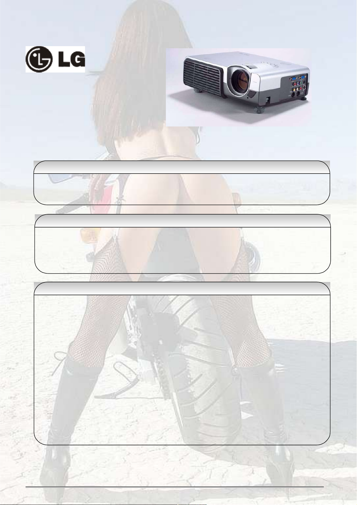
LG RD-JT40/41 Service Manual
RD-JT40/RD-JT41
SERVICE MANUAL
Caution
Be sure to read this manual before servicing. To assure safety from fire, electric shock, injury, harmful
radiation and materials, various measures are provided in this Acer DLP projector. Be sure to read
cautionary items described in the manual to maintain safety before servicing.
Service Warning
1. When replace the lamp, to avoid burns to yor fingers. The lamp becomes too hot.
2. Nevr touch the lamp bulbwith a finger or anything else. Never drop it or give it a shock. They may cause
bursting of the bulb.
3. This projector is provided with a high voltage circuit for the lamp. Do not touch the electric parts of
powrer unit (main), when turn on the pojector.
4. Do not touch the exhaust fan, during operation.
Contents
1. Specifications............................................................................................................................................2
2. Spare Parts List .......................................................................................................................................4
3. Shipping Cntents......................................................................................................................................5
4. Projector Dsription....................................................................................................................................6
5. Rmote Control Desription.........................................................................................................................9
6. Insallation................................................................................................................................................11
7. Operation................................................................................................................................................13
8. Shutdown................................................................................................................................................21
9. Maintenance...........................................................................................................................................22
10. Lamp Replacement..............................................................................................................................23
11. Trouble Shooting..................................................................................................................................25
12. Timing Char..........................................................................................................................................33
13. DMD Image Secification.......................................................................................................................34
14. Electrical nterface Caracter..................................................................................................................37
15. Final Assembly Alignent Procedure......................................................................................................39
16. Pakng Description................................................................................................................................44
17. Appearance Description.......................................................................................................................45
18. Dimension ............................................................................................................................................47
19. Schematics ..........................................................................................................................................48
20. Assy Drawing .......................................................................................................................................85
1
Page 2

LG RD-JT40/41 Service Manual
1. SPECIFICATIONS
Projector Specifications
Technical Specifications
Note: All specifications are subject to change without notice.
General
Product name Personal Projector
Model name RD-JT40 1024*768XGA
RD-JT41 800*600SVGA
Optical
Display system 1-CHIP DMD
Lens F/Number F/2.6
Lamp 210W NSH lamp
Electrical
Power supply AC100 ~ 240V, 3.5A, 50/60 Hz (Automatic)
Power consumption 330 W (Max)
Mechanical
Dimensions 308mm/12in (W) x 95mm/3.7in (H) x 238mm/9.4in (D)
Operating temperature range
10 C ~ 40 C
Weight 6.9 lbs (3.1 Kg)
Input terminal
Computer input
RGB input D-sub 15-pin (female)
Video signal input
S-VIDEO Mini DIN 4-pin port x1
VIDEO RCA jack x1
HDTV signal input YPBPR RCA jack x3
Audio signal input
Audio 1 Mini jack stero port
Audio 2 RCA jack L, R x2
Output
USB mouse connector A/B series x1
Speaker 2 watt x 1
Control
RS-232C 9-pin x1
2
Page 3

LG RD-JT40/41 Service Manual
Service Information
Accessories (included in the Standard Package)
Description of parts Part No.
Power cord (EU)
Power cord (US)
27.82718.281
27.01818.000
Power cord (UK) 27.01018.000
VGA signal cable 50.J0508.502
Video cable 50.73213.501
S-Video cable 50.72920.011
PC audio cable 50.74405.501
Soft carrying case 98.J3402.001
HDTV cable 50.J2401.001
USB mouse cable 50.73213.501
Remote control
98.J3401.001
3-2 converter 22.91007.011
Optional Accessories (not included in the Standard Package)
Description of parts Part No.
Mac adapter (switchable) 20.20118.A15
Spare lamp module 60.J3416.CB1
3
Page 4

LG RD-JT40/41 Service Manual
2. Spare Parts List
Item No:99.J3477.L11Projector LGRD-JT40 spare parts list
Parts No Description
55.J3405.001 PCBA FAN CONTROL/B DX660
55.J3408.001 PCBA DC-DC/B DX660
60.J3419.001 ASSY PFC MODULE DX660
55.J3407.001 PCBA PFC CONTROL/B DX660
60.J3477.L11 ASSY ENGINE DX660-L11
55.J3419.001 PCBA THERMAL/B DX660
60.J3403.021 ASSY LOWER CASE P838 DX660/LG
42.J3415.001 FOOT REAR SILICON BLA. DX660
65.J3406.001 ADJUST FOOT FRONT MARS
55.J3401.001 PCBA DMD/B DX660
55.J3402.031 PCBA MAIN/BD LG DX660
60.J3414.031 ASSY OPTICAL ENG. DX660/LG
55.J3404.001 PCBA CHIP/B DX660
60.J3415.021 ASSY HSG DMD DX660/LG
71.01076.001 IC DIGITA IMAG DMD1076-7LGA11
60.J3404.001 ASSY BALLAST MODULE DX660
60.J3405.002 ASSY REAR FAN HLD MODULE DX66
60.J3407.021 ASSY REAR CVR MODULE DX660/LG
60.J3409.001 ASSY CAP LENS TRANS. DX660
60.J3412.061 ASSY UPPER CASE P896 DX660/LG
55.J3403.001 PCBA KEYPAD BD DX660
60.J3416.001 ASSY LAMP MODULE U DX660
60.J3482.001 ASSY REMOTE+CABLE LG DXS660
27.01018.000 CORD H05VV-F 13A250V 1830MM U
27.01818.000 CORD SVT#18*3C 10A125V 1830US
27.82718.281 CORD H05VV-F 10A250V EUR BLK
50.73213.501 CABLE 4P USB A-B 1800MM BLACK
50.J0508.502 SIGNAL/C 15/15P 2500MM/BLK
50.J7111.501 CABLE A/V (G.B.R)1800 BLK 784
50.72918.001 CABLE A/V RCA(R,W,Y)1500MM
50.72920.011 C.A MIN-DIN 4P S-VIDEO W/S 15
50.74405.501 CABLE AUD PC99PT284C/PT577C B
98.J3403.001 REMOTE CONTROLLER DXS660 LG
98.J3404.001 SOFT CASE DXS660 LG
Item No:99.J3877.L11Projector LGRD-JT41 spare parts list
4
Page 5

LG RD-JT40/41 Service Manual
Parts No Description
55.J3405.001 PCBA FAN CONTROL/B DX660
55.J3408.001 PCBA DC-DC/B DX660
60.J3419.001 ASSY PFC MODULE DX660
55.J3407.001 PCBA PFC CONTROL/B DX660
60.J3877.L11 ASSY ENGINE DS660-L11
55.J3419.001 PCBA THERMAL/B DX660
60.J3403.021 ASSY LOWER CASE P838 DX660/LG
42.J3415.001 FOOT REAR SILICON BLA. DX660
65.J3406.001 ADJUST FOOT FRONT MARS
60.J3406.061 ASSY INTERFACE MODULE DS660/L
55.J3801.001 PCBA DMD/BD FOR DS660
55.J3804.M21PCBA MAIN/BD FOR LG DS660
60.J3410.001 ASSY BOX LAMP DX660
60.J3411.001 ASSY BKT BLOWER DX660
60.J3414.041 ASSY OPTICAL ENG. DS660/LG
55.J3802.001 PCBA DMD CHIP/BD FOR DS660
60.J3415.021 ASSY HSG DMD DX660/LG
71.08460.000 IC DIGITAL IMAG DMD8460 LGA11
60.J3404.001 ASSY BALLAST MODULE DX660
60.J3405.002 ASSY REAR FAN HLD MODULE DX660
60.J3407.021 ASSY REAR CVR MODULE DX660/LG
60.J3409.001 ASSY CAP LENS TRANS. DX660
60.J3412.071 ASSY UPPER CASE P896 DS660/LG
55.J3403.001 PCBA KEYPAD BD DX660
60.J3413.071 ASSY SUB U/C P896 DS660/LG
60.J3416.001 ASSY LAMP MODULE U DX660
60.J3417.021 ASSY DOOR LAMP P838 DX660/LG
60.J3481.001 ASSY MANU+WARRANTY LG
60.J3482.001 ASSY REMOTE+CABLE LG DXS660
98.J3403.001 REMOTE CONTROLLER DXS660 LG
98.J3404.001 SOFT CASE DXS660 LG
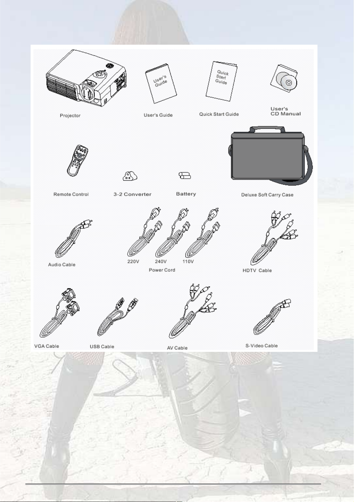
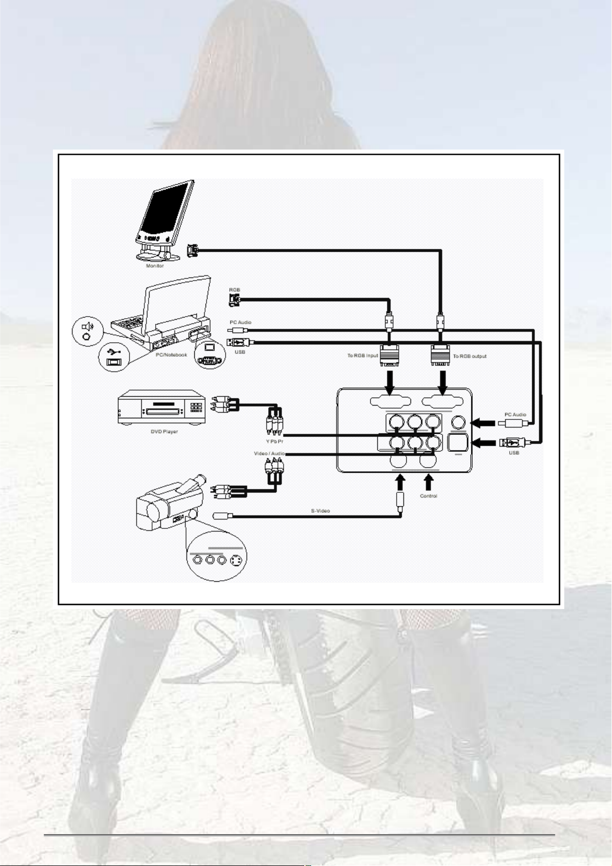
3. Shipping Contents
The Projector is shipped with the cables required for connection to standard PC or laptop
computers. Carefully unpack and verify that you have all the items shown below. If any of
these items are missing, please contact personnel at the place of purchase.
5
Page 6
LG RD-JT40/41 Service Manual
Optional Accessories
1. Macintosh adapter
2. 210W Lamp module
4. Projector Description
Projector
6
Page 7
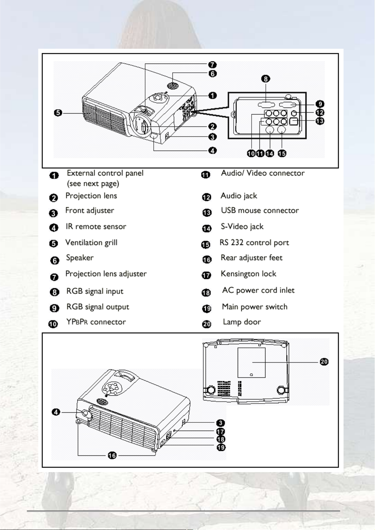
LG RD-JT40/41 Service Manual
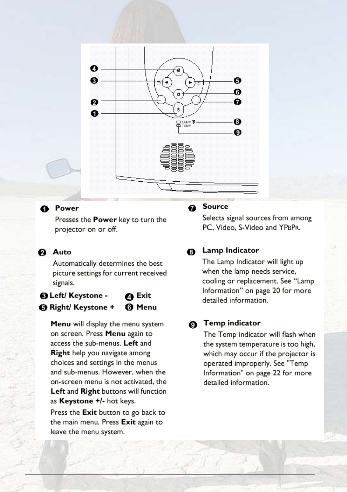
External Control Panel
7
Page 8
LG RD-JT40/41 Service Manual
Adjuster
8
Page 9
LG RD-JT40/41 Service Manual
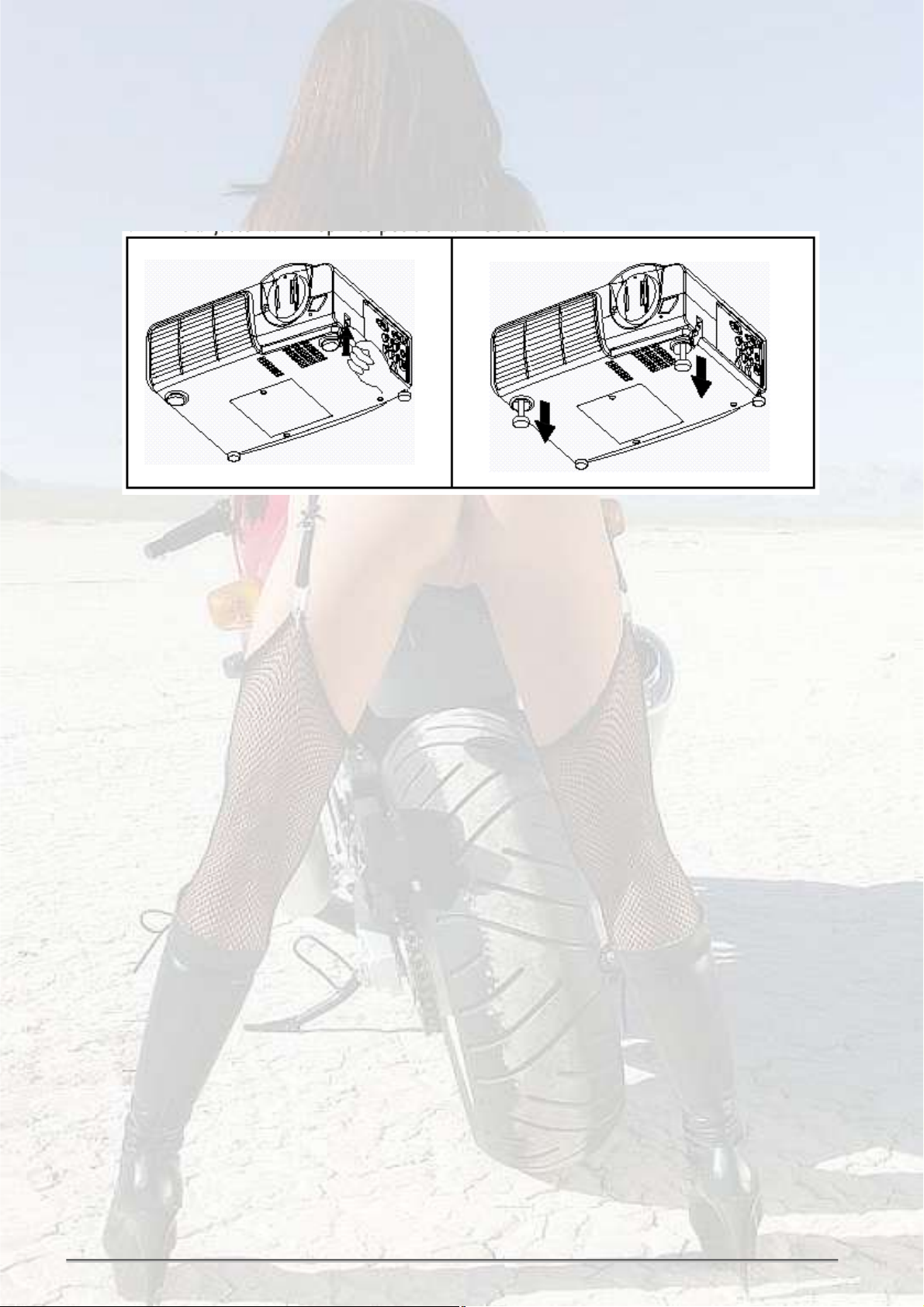
The projector is equipped with 2 quick-release adjuster feet. Push the buttons to adjust its tilt
angle.
1. Lift the projector up and press the adjuster button to release the adjuster.
2. The adjuster will drop into position and be locked.
Projector Features
The projector integrates high-performance optical engine projection and a user-friendly design
to deliver high reliability and ease of use. The projector offers the following features:
Small and light for portability
Full-function remote control with laser pointer/ remote mouse function
Hight quality manual zoom lens
One-key auto-adjustment to display the best picture quality
Easy digital keystone correction through hot keys to correct distorted images
Adjustable color balance control for data/video display
Ultra-high brightness projection lamp
Ability to display 16.7 million colors
On-screen menus in 8 languages: English, French, German, Italian, Spanish, Korean,
Simplified Chinese, and Traditional Chinese.
Switchable Normal/ Video mode for data/ video display
Powerful AV function to provide high quality AV picture
HDTV compatibility (YPBPR)
Note: The brightness of the projected image will vary depending on the
ambient lighting conditions and contrast/brightness settings.
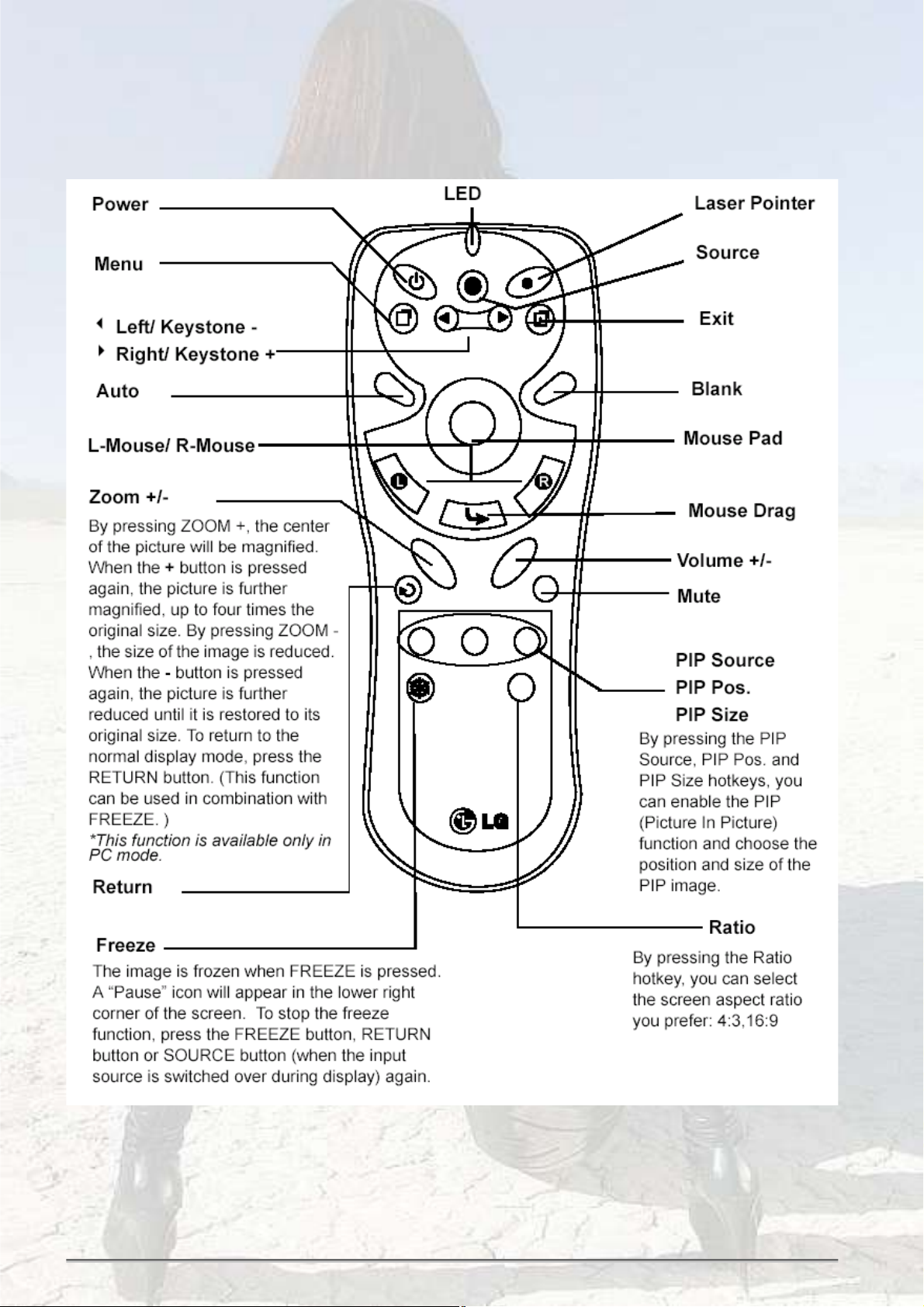
5. Remote Control Description
9
Page 10
LG RD-JT40/41 Service Manual
The remote control sensors are located in the front/ back of the projector. The distance
between the sensor and the remote control should not exceed 6 meters.
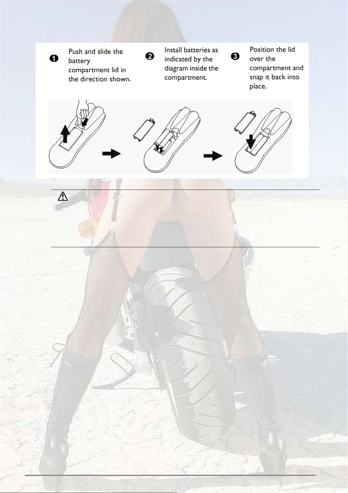
Installing or Replacing Batteries
10
Page 11
LG RD-JT40/41 Service Manual
Caution
Avoid excessive heat and humidity. There may be danger of an explosion if batteries
are incorrectly replaced. Replace only with the same or equivalent type recommended
by the manufacturer. Dispose of used batteries according to the manufacturer!s
instructions.
11
Page 12
LG RD-JT40/41 Service Manual
6. INSTALLATION
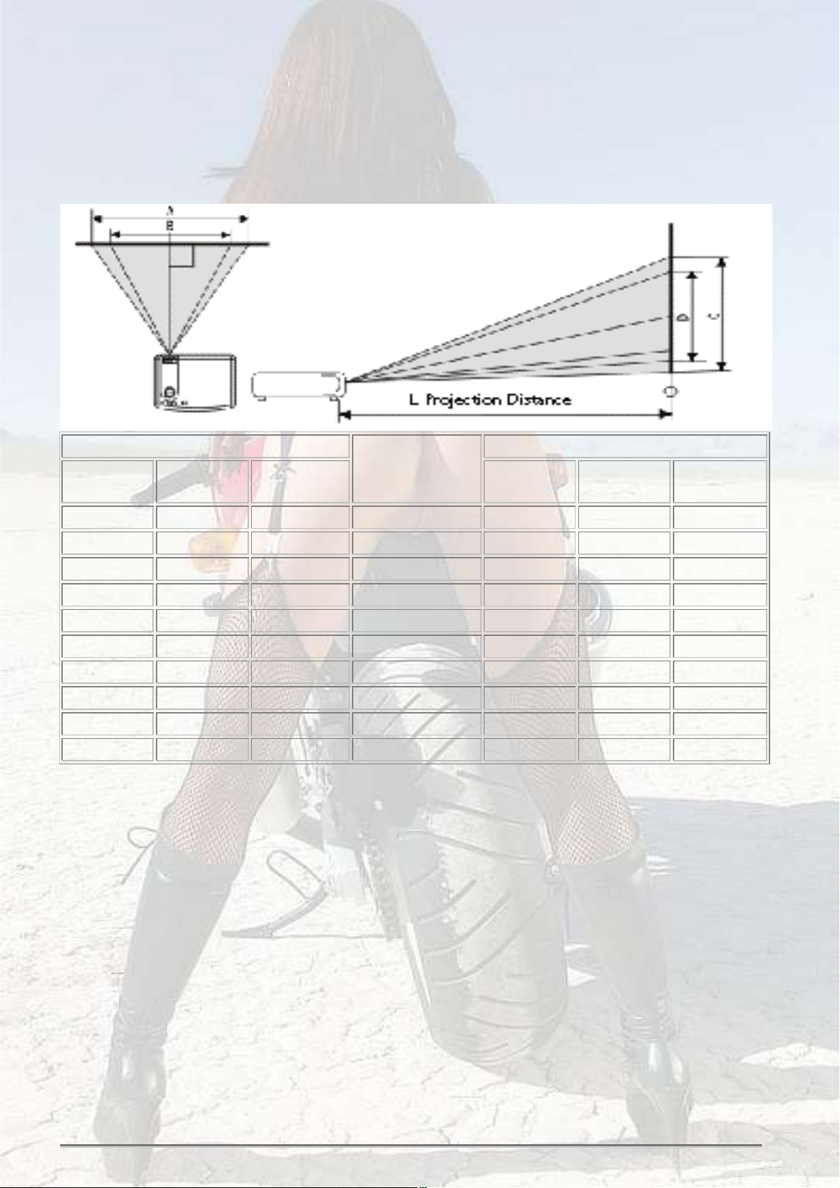
Screen Size
Place the projector at the required distance from the screen according to the desired picture size
(see the table below).
Diagonal
(cm/in)
Screen Size (Max.) Screen Size (Min.)
A. Width
(cm/in)
C. Height
(cm/in)
L. Projection
distance (cm/in)
Diagonal
(cm/in)
B. Width
(cm/in)
D. Height
(cm/in)
77/30.4 61.8/24 46.3/18 100/39 63/24.9 50.7/20 38.0/15
154/60.8 123.65/49 92.7/36 200/79 127/49.9 101.3/40 76.0/30
232/91.2 185.3/73 138.9/55 300/118 190/74.7 151.9/60 113.9/45
309/121.5 247.0/97 185.2/73 400/157 253/99.7 202.5/80 151.9/60
386/151.9 308.7/122 231.6/91 500/197 316/124.6 253.2/100 189.9/75
463/182.3 370.5/146 277.9/109 600/236 380/149.5 303.8/120 227.9/90
541/213.1 432.2/170 324.18/128 700/276 443/174.6 354.4/140 266.2/105
617/243.1 494.0/194 370.5/146 800/315 506/199.4 405.1/160 303.8/120
695/273.5 555.7/219 416.7/164 900/354 570/224.3 455.7/180 341.8/135
772/303.9 617.5/243 463.11/182 1000/394 633/249.2 506.3/200 379.8/150
Connecting to Various Equipment
HDTV description
The projector is capable of displaying various High Definition TV display modes. Some of
these sources are:
Digital-VHS (D-VHS) player DVD player
Satellite Dish HDTV receiver DTV tuners
Most of these sources will provide an analog component video output, a standard VGA
output, or a YPBPR (default) format.
The projector is capable of accepting HDTV data through a YPBPR connector. Use a
HDTV cable that came with your projector to display HDTV images.
The following standards are supported in the HDTV function:
480i 480p
720p 1080i
Please refer to "Menu System" on page 13 for information on the HDTV OSD selections.
12
Page 13
LG RD-JT40/41 Service Manual
Connecting to Various Equipment
It only takes a few seconds to connect your projector to your desktop or notebook computer, VCR,
or other systems. However, a Mac adapter (an optional accessory) is needed for connection to
Macintosh computers.
13
Page 14
LG RD-JT40/41 Service Manual
7. OPERATION
Start Up
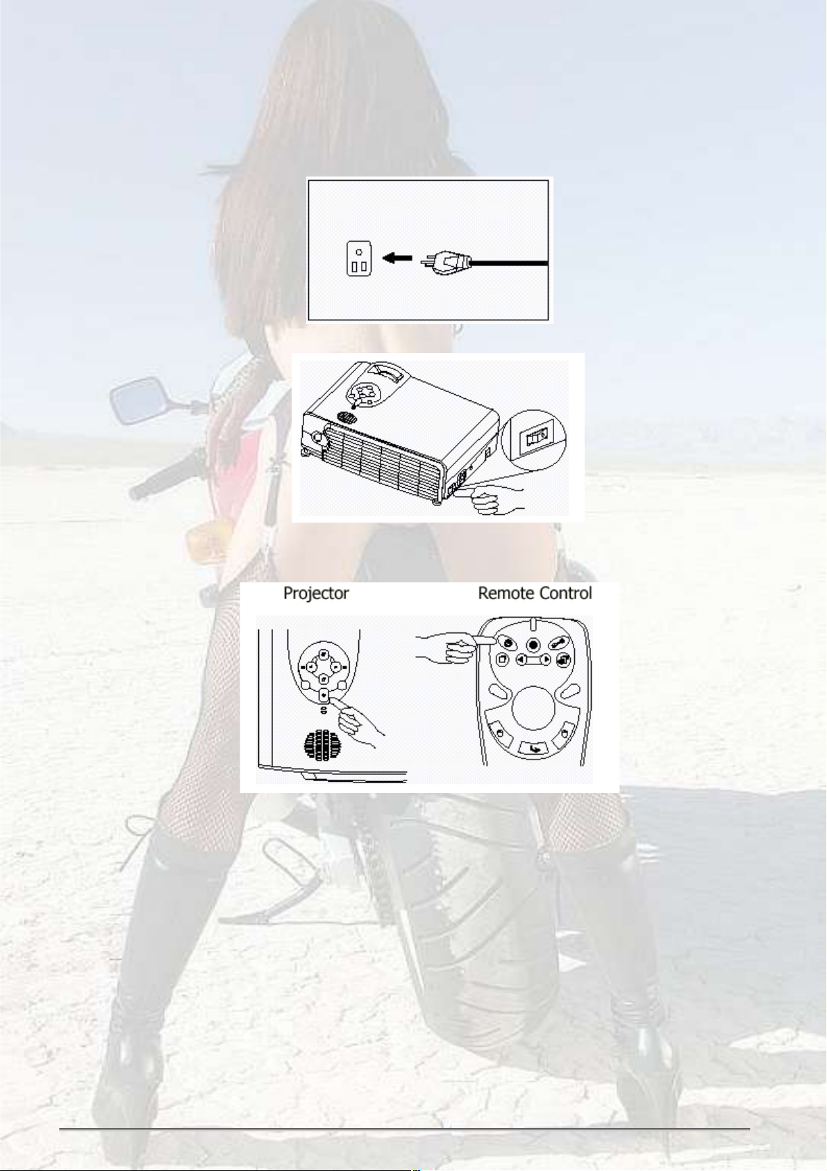
1. Plug the power cord into a wall socket.
2. Turn on the main power switch.
3. Press POWER to start the unit. The back-lit POWER key flashes green and stays green
when the power is turned on
(When the power is turned off, there is a 60-second cooling period before the projector can be
re-started.)
4. Switch on all connected equipment.
14
Page 15
LG RD-JT40/41 Service Manual
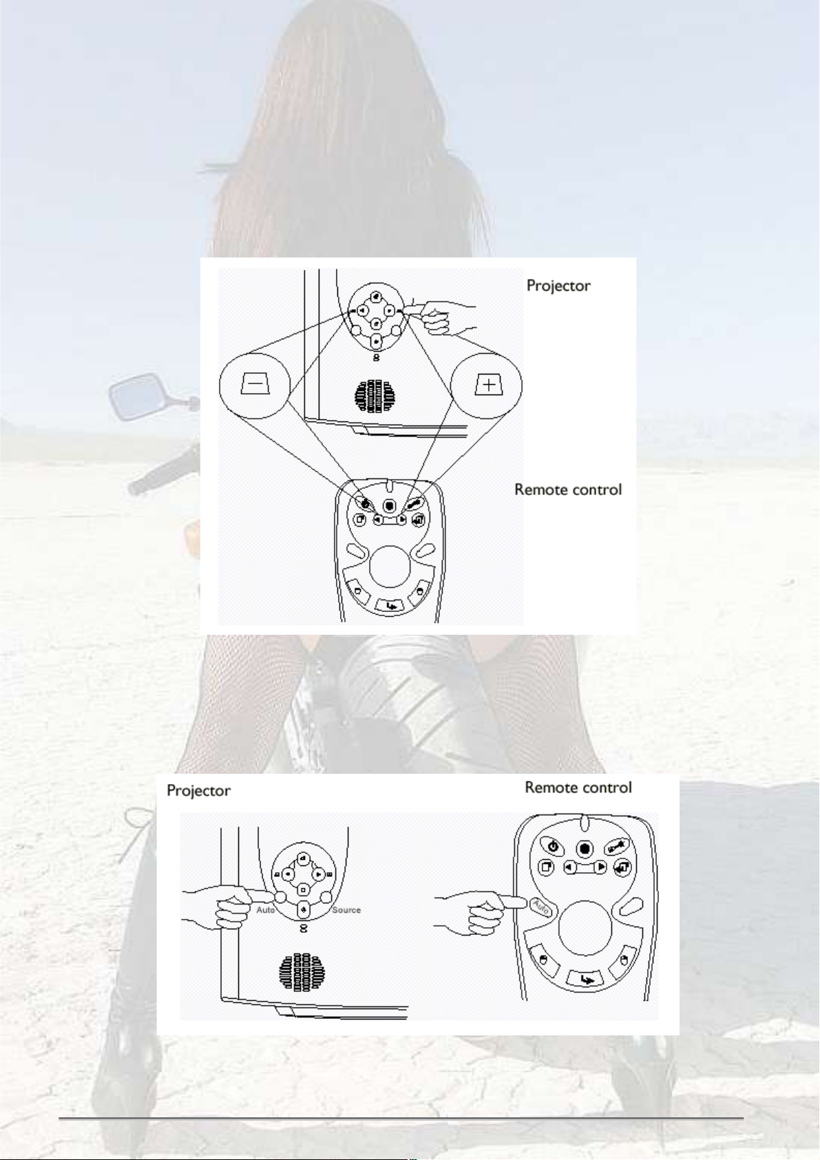
Digital Keystone Correction
Keystoning refers to the situation where the projected image is noticeably wider at either the
top or bottom. To correct this, press KEYSTONE +/- (hot key) on the control panel of the
projector or on the remote control, and then adjust the sliding bar labeled Keystone, as
needed. Press + to correct keystoning at the top of the image. Press - to correct keystoning
at the bottom of the image.
Auto Adjustment
In some cases, you may need to optimize the picture quality. To do this, press the AUTO key
on the control panel of the projector or on the remote control. Within 3 seconds, the built-in
Intelligent Auto Adjustment function will re-adjust settings to provide the best picture quality.
15
Page 16
LG RD-JT40/41 Service Manual
Source Selection
When several input sources are available, press the SOURCE key to make a selection from the
control panel of the projector or the remote control.
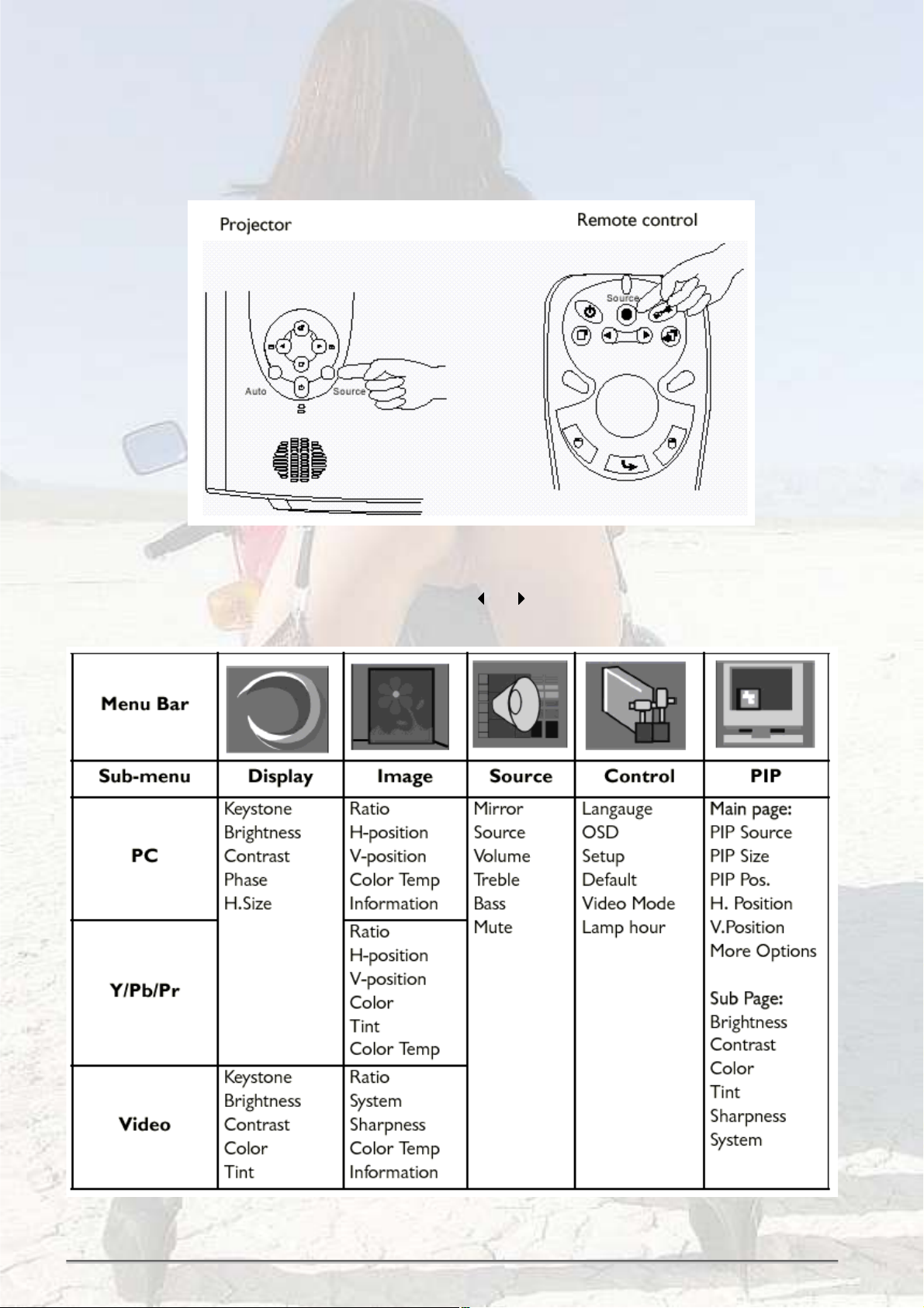
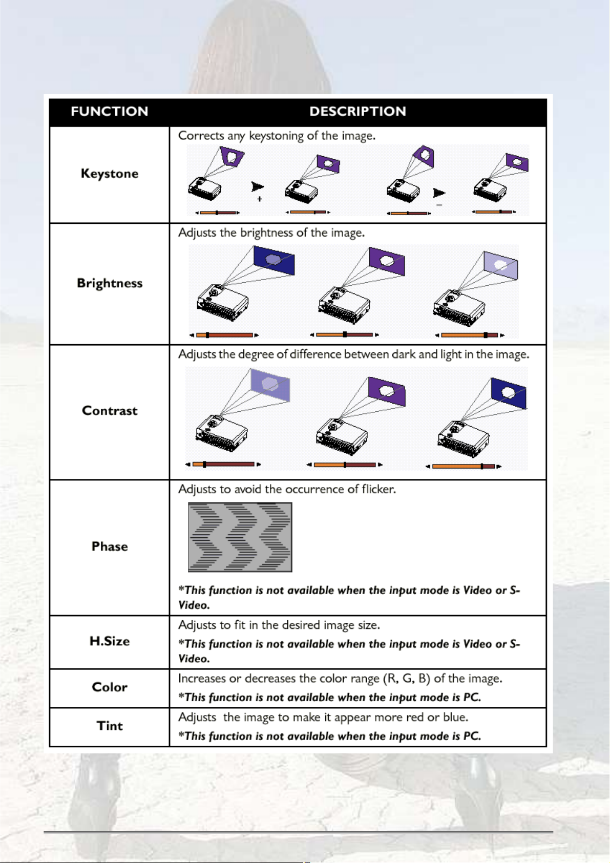
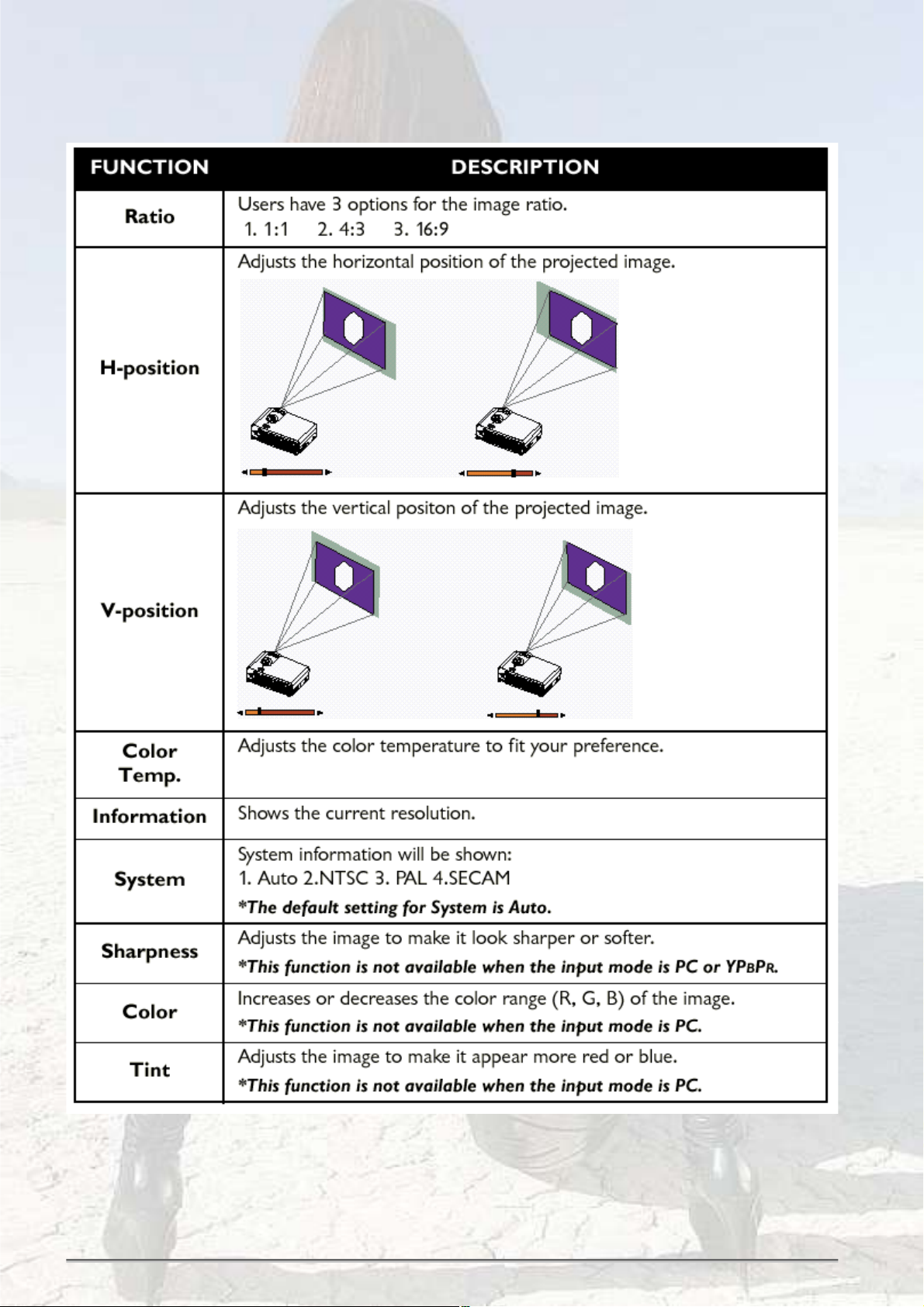
Menu System
Press Menu for the main menu, and then press or to select a sub-menu. Press Menu
again to select items in the sub-menu.
16
Page 17
LG RD-JT40/41 Service Manual
1. Display Menu
17
Page 18
LG RD-JT40/41 Service Manual
2. Image Menu
18
Page 19
LG RD-JT40/41 Service Manual
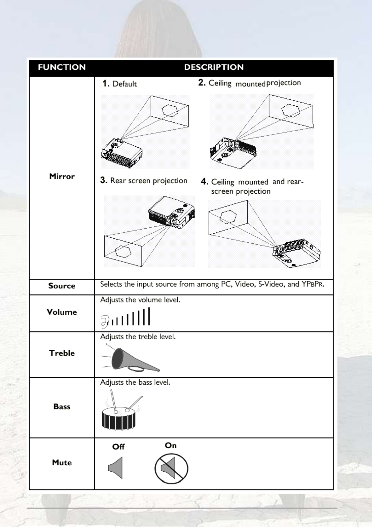
3. Source Menu
19
Page 20

LG RD-JT40/41 Service Manual
4. Control Menu
FUNCTION DESCRIPTION
Language sets the language for the OSD control menus.
Language
Use the 3 / 4 key to select the desired language from among English, French, German,
Italian, Spanish, Korean, Simplified Chinese and Traditional Chinese.
OSD Pos.
Selects a desired OSD position.
OSD
OSD Time
Sets the length of time the OSD will remain active after the last time you pressed the
button. The range is from 5 to 60 seconds in 5-second increments.
Source scan
When selected, activates the Source scan function.
Keystone hold
When selected, preserves the last keystone correction value even when the projector is
restarted.
Setup
Default
Video Mode
Lamp hour
Mirror hold
When selected, preserves the last mirror correction value even when the projector is
restarted.
Blank time
Determines the length of time before the projector is shut off when Blank is activated.
Auto off
Sets the length of time before the system is shut off when no input is detected.
User logo
Enables the user to define the logo screen that will display during start-up. Three modes
are available: Default (BOXLIGHT logo), black screen and blue screen.
Returns all settings to their factory preset values.
Selects video mode.
Shows lamp usage time.
20
Page 21
LG RD-JT40/41 Service Manual
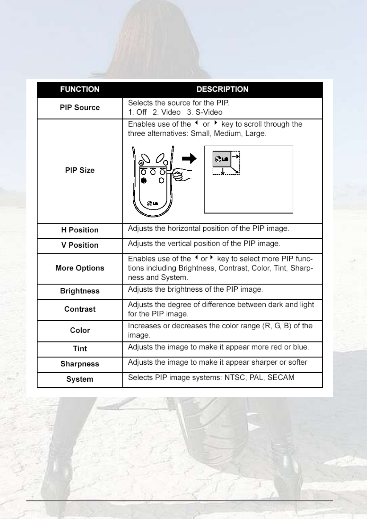
5. PIP Menu
These functions are available only when the input mode is PC and the PIP source is Video or
S-Video
21
Page 22
LG RD-JT40/41 Service Manual
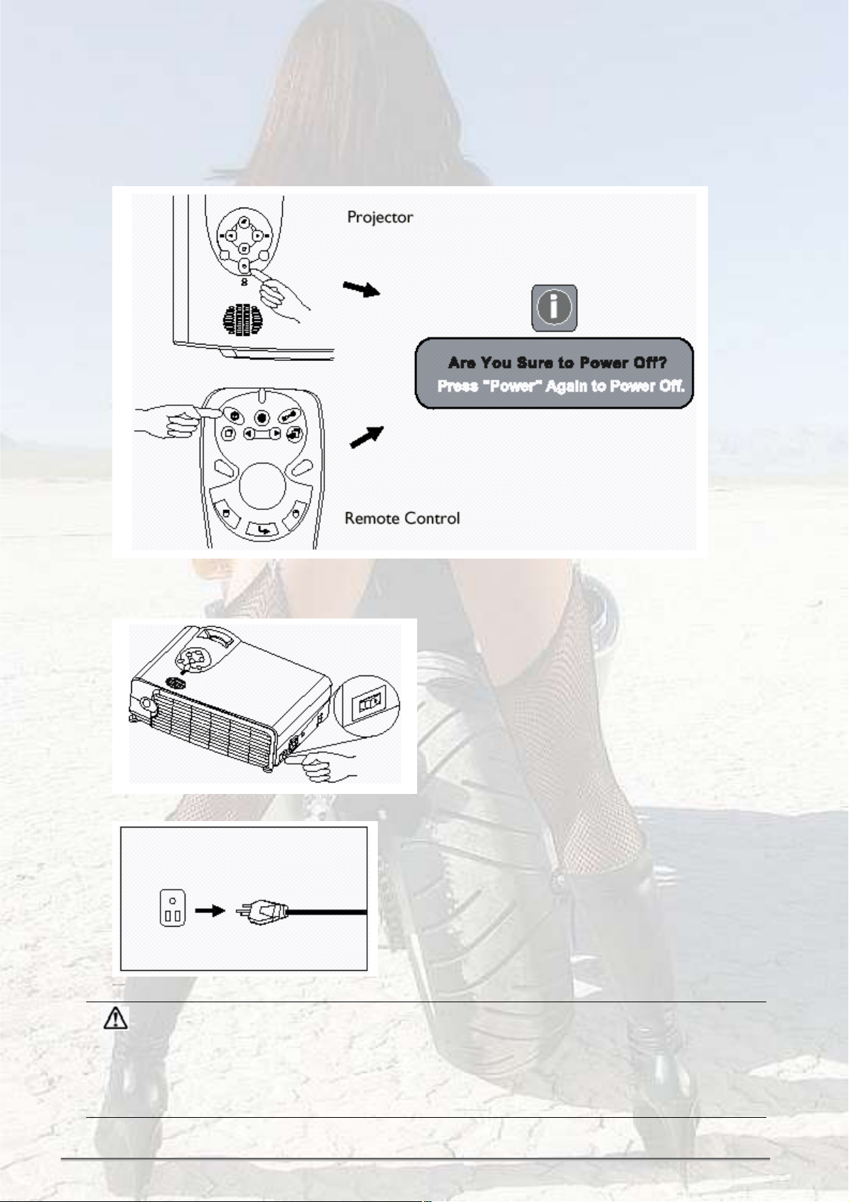
8. Shutdown
1. Press POWER and a warning message will appear. To turn off the projector, press
POWER again.
2. The fan will continue to run for approximately two minutes.
3. Turn off the main power switch.
4. Disconnect the power cord from the wall socket.
Caution
Please do not unplug the power cord before POWER is shut down or during the two-minute cooling
process. If the projector is not properly shut down, to protect the lamp, the system will detect this and
cool the lamp for two minutes automatically before turning on again.
22
Page 23

LG RD-JT40/41 Service Manual
9. MAINTENANCE
Lamp Information
Use and Replacement of the Lamp
When the lamp Indicator lights up red or a message appears suggesting the time of
lamp replacement, please install a new lamp or consult your dealer. An old lamp
could cause a malfunction in the projector and in rare instances may even explode.
Lamp LED Indicators
Lamp Life Indicators When the LED lights up red, it is warning you
The Lamp is not properly
attached
The temperature is too high When the projector!s internal temperature is too
that lamp usage has exceeded 1500 hours.
Replace the projection lamp with a new one
immediately.
LED lights up red.
high for the projector to operate safely, the LED
blinks orange and the lamp turns off
automatically. The LED keeps blinking while
the unit is off. If the LED light is off, the
operation and temperature of the projector!s
lamp are normal.
Caution
The LAMP indicator will light up if the lamp becomes too hot. Turn off the power and let the
projector cool for 45 minutes. If the LAMP indicator is still red when turning the power on, please
contact your dealer.
23
Page 24
LG RD-JT40/41 Service Manual
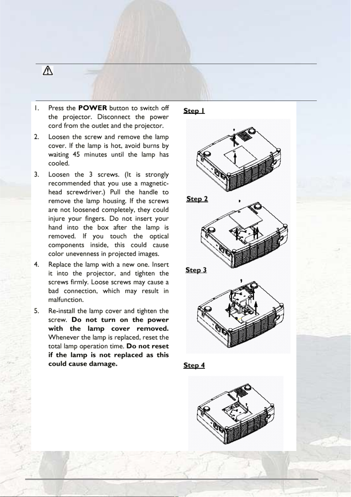
10. Lamp Replacement
Caution
To reduce the risk of electrical shock, always turn off the projector and disconnect the power cord before
changing the lamp
24
Page 25
LG RD-JT40/41 Service Manual
Caution
To reduce the risk of severe burns, allow the projector to cool for at least 45 minutes before replacing
the lamp.
The reduce the risk of injuries to fingers and damage to internal components, use caution when
removing lamp glass that has shattered into sharp pieces.
To reduce the risk of injuries to fingers and/or compromising image quality by touching the lens, do not
touch the empty lamp compartment when the lamp is removed.
This lamp contains mercury. Consult your local hazardous waste regulations to dispose of this lamp in
a proper manner.
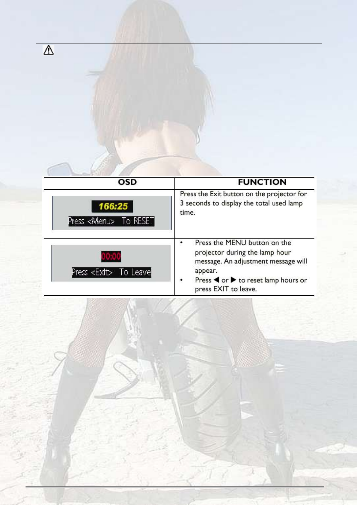
Resetting Lamp Hours
If you replace the lamp after 1500hours of operation, please follow the instructions
below within 10 minutes of powering on.
Temp Information
When the LED lights up, it is warning you of the following possible problems:
1. The internal temperature is too high.
2. The fans are not working.
Turn off the projector and contact qualified service personnel for further help.
25
Page 26

LG RD-JT40/41 Service Manual
11. TROUBLE SHOOTING
Common Problems & Solutions
PROBLEMS TRY THESE SOLUTIONS
NO POWER
NO PICTURE
TRAPEZOID IMAGE ON
THE SCREEN
POOR COLOR
BLURRED IMAGE Press Auto on the control panel of the projector or the
REMOTE CONTROL
DOES NOT WORK
Make sure the power cord is inserted snuged into the AC
adapter socket.
Make sure the power cord is inserted snuged into the power
outlet.
Toggle the power switch to the position "I#
Wait two minutes after the projector is turned off before
turning the projector back on.
Check for the proper input source.
Ensure all cables are connected properly.
Adjust the brightness and contrast.
Remove the lens cap.
Reposition the unit to improve its angle on the screen.
Use the Keystone correction key on the control panel of
the projector or the remote control unit.
Select the correct video system.
Adjust brightness, contrast, or saturation.
remote control unit to get better picture quality.
Adjust the focus.
Reposition the unit to improve its projection angle.
Ensure the distance between the unit and screen is within
the adjustment range of the lens.
Replace the batteries with new ones.
Make sure there is no obstacle between the remote
control and the projector.
Stand within 4 meters (13 feet) of the projector.
Make sure nothing is blocking the front and rear receivers.
Status Messages
On-Screen Messages Description
SEARCHING Projector is searching for input.
ACQUIRING SIGNAL
OUT OF RANGE Input signal frequency exceeds the projector!s range.
LAMP WARNING
CHANGE LAMP AND
RESET LAMP TIMER!
OUT OF LAMP USAGE
TIME. CHANGE THE
LAMP!
OUT OF LAMP USAGE
TIME. YOU HAVE TO
CHANGE THE LAMP!
Projector has identified the input signal and is running the auto
image adjustment function.
The lamp has been in operation for 1400 hours. Install a new
lamp for optimal performance.
The lamp has been in operation for 1480 hours, and the power
will turn off after 20 hours.
The lamp has been in operation for over 1500 hours. The
warning message will display for 30 seconds every 5 minutes
after you turn on the projector and the power will turn off
automatically after 10 minutes.
26
Page 27

LG RD-JT40/41 Service Manual
1. Final Assembly Trouble Shooting Guide
System Trouble Shooting Flow Char
STEP:
Back-LIGHT OK?
No
1.Check power core
2.Check power board and wire
Yes
Power ON OK?
(LAMP ON?)
Yes
No Signal?
No
Auto Power Off?
No
Video NG? Yes
No
Yes
Yes
1.Check lamp door.
2.Check thermal switch and wire
3.Check 12V Fan and wire
4.Check power board and wire
5.Check color wheel FPC
6.Check screws on color wheel
7.Check color wheel motor
8.Check DMD driver board and 120 pins connector
9.Check Translation board and wire and 50 pins connector
10.Check Main board
11.Check AV Box connector (if with this option)
1.Check input cable
2.Check OSD source set up
1.Check OSD lamp hours
2.Check OSD Auto Off setup value
3.Check lamp door
4.Check 12V fan
5.Check thermal status
6.Check AV Box connector(if with this option)
1.Check AV Box
2.Check Video cable
No
Audio NG?
No
IR Remote Control
NG?
No
Pixel Fail?
No
Image NG?
(Raindrops)
No
A
Yes
Yes
Yes
Yes
1.Check AV Box
2.Check audio cable
1.Check Remote module battery
2.Check Remote module
3.Check Translation board
4.Check Main board
1.Check DMD chip
2.Check DMD board
1.Check color wheel and Sensor board
2.Check DMD chip and holder
3.Check DMD conductive elastomers assembling
4.Clean DMD conductive elastomers
27
Page 28

LG RD-JT40/41 Service Manual
2. Engine Assembly Trouble Shooting Guide
A
1.Check DMD board
Image NG?
(Blank)
No
Yes
2.Check color wheel and Sensor board
3.Check DMD conductive elastomers
4.Check Main and Translation boards
Image NG?
(Screen flashing)
No
Image NG?
(Screen dimmish)
No
Image NG?
(Freezing)
No
Yes
Yes
Yes
1.Check color wheel and Sensor board
2.Check DMD board
3.Check Main and Translation boards
1.Check DMD board
2.Check color wheel and Sensor board
1.Check color wheel
2.Check Sensor board color index signal
Image NG?
(Missing column bar)
No
Image NG?
(Screen overlap)
Yes
Yes
1.Check DMD holder
1.Check Main and Translation boards
2.Check DMD board
28
Page 29

LG RD-JT40/41 Service Manual
Start
Power On
OK
NG
1.chk CW
2.chk DMD/b
3.chk Main/b
4.chk TR/b
Image Quality
OK
EE
Performance
OK
Optical
Performance
NG
NG
Dust
No
Blue Edge
Brightness
System
Trouble
shooting
Guide
No
No
Focus NG
No
Pixel Failure
YesNG
1.clean DMD chip
Yes
Yes
Yes
Yes
No
light leakage
1.Reset Factory mode, chk DC offset/Gain setup
2.chk DMD/b
3.clean projection lens
4.cleanTIR
5.clean optical parts
Yes
2.clean TIR(DMD
side)
1.chk lens housing / DMD
housing Assembly
2.chk light pipe assembly
3.chk TIR assembly
4,change light pipe clip
5.change light pipe
change projection
1.change DMD
2.change DMD/b
3.clean elastomer
1.chk DMD baffle
2.chk TIR
lens
Uniformity
No
Contrast
No
Color
No
Color
Uniformity
Yes
Yes
Yes
Yes
1.chk TIR
2.chk projection lens
1.Reset Factory mode, chk DC offset/Gain setup
2.chk DMD baffle
3.change projection lens
1.Reset Factory mode, chk CW delay
2.change CW
3.change projection lens
1.chk TIR
2.chk DMD
3.chk DMD/b
29
Page 30

LG RD-JT40/41 Service Manual
3. Main Board Trouble Shooting Guide
System no work
No
Yes
a . IC201 bad soldiering
b. Flash(IC201) without software inside.
c. IC607(Reset IC) function abnormal
d. IC901 no work.
a. Check IC609 (3.3V) or IC610(2.5V)
b. Check MCLK and DCLK
No data signal
output to DMD BD
No
The image display
"No Signal" when
the input is PC
No
The ghost Image
display output of
Video input
No
Couldn't download
new software to
MianBD
No
Remote mouse
don't work
Yes
Yes
Yes
Yes
Yes
a. IC901 bad soldiering causing IC901 no work.
b. Check IC609(3.3V) or IC610(2.5V).
c. Check IC203, IC202 if there was MCLK and DCLK
output to IC901.
a. Check the voltage of IC502, IC503(3.3V),
IC501(3.3V), BC537(3.3V)
b. if voltage above are OK, then check
IC611(VSYNC) and IC606(HSYNC) if there were
these two signal or not.
c. Replace IC502
a.CN605 bad soldiering
b.IC901 bad soldiering
c.Avbox and MainBD bad connection
a. Replace IC602
b. IC901
a.Check the mouse of PC is still working normally
b.Check the mouse driver of PC is PS2 compatible
mouse
c.Replace IC802
No
Keypad working
abnormally
No
LampLit signal
abnormal
No
IR doesn't work.
No
Gray bar abnormal or
image contour(PC input)
Yes
Yes
Yes
Yes
Check IC613
Check IC612
a.Check soldiering condition of R692.
b.IC901 bad soldiering
Check the resisters between IC502 and IC901
(RP501 RP512)
30
Page 31

LG RD-JT40/41 Service Manual
4. Power Supply Trouble Shooting Guide
YES CHECK SPS B/D.
INPUT
B + B380VDC
WHETHER POOR
SOLDER
LINE
0VACOR
220VAC
NO
B + B-
54VDC
NO
B + B0VDC
NO
CHECK
R663,R662,
R66 ,R659,
R660,ZD65
YES
CHECK PFC B/D.
WHETHER POOR
SOLDER
YES
CHECK L65
L652
WHETHER
POOR SOLDER
F65
OPEN
NO
YES
Q65 DAMAGE
(D.S. SHORT)
NO
Q60 DAMAGE
(D.S. SHORT)
YES
YES
CHECK IC65
R656,D65
BD65 ,R658
R678
CHECK
R6 2,R609
D6 0,IC60
R6 ,Q602
NO
CHECK
POLARITY :
B+ PGND,
B + B-,
C659
31
Page 32

LG RD-JT40/41 Service Manual
5. Translation Board Trouble Shooting Guide
DS660 Translation Board Trouble Shooting Guide
VCCCPU OK
POWERONA
function OK?
Yes
VCC,12V
function OK?
Yes
Abnormal
function
OK?
Yes
LAMPEN-S
function OK?
Yes
LAMP_LIT
function OK?
No
No
No IC806
No
No
1.Q803
2.Q703,Q704
1.Q705
2.Q706
3.Q701
4.Q702
1.Q802
2.IC805
1.Q707
2.Q708
Yes
IR0 function
OK?
Yes
LED_1~3,
FAN_HSO
function OK?
Yes
VPOSRAIL,
VNEGRAIL
function OK?
Yes
END
No
No IC802
No
1.IC802
2.IC803
1. Q15
2. Q9
3. D8
4. D10
5. U2
6. D12
7. D11
8. D9
32
Page 33

LG RD-JT40/41 Service Manual
6. DMD Board Trouble Shooting Guide
Check power voltages.
Check clocks from oscillator (58 MHz), from ASIC (58 MHz and 116 MHz), from FPGA (9.667
MHz and 2.4 MHz), to Hitachi (14 MHz), to motor controller (9.667 MHz)
Verify HSYNC, VSYNC, ACTDATA, SYNCVALID, POWERGOOD, RESETZ from computer or
source at 60 Hz. Verify these signals meet TI specified timing per Hardware ICD.
Verify color wheel index running at 120 Hz
If no color wheel spinning, check data transfer on the following lines: MTRDATA, MTRCLK,
MTRSELZ.
Verify phase lock of color wheel by checking rising edge of Index 275 us after Vsync
If previous steps are verified, microcontroller is OK.
Verify motor_spin line from microcontroller to FPGA is logic high.
Verify hardware LAMPEN to ballast. Lamp type must be set to appropriate type if problems with
getting LAMPLIT appear.
3.5 seconds after LAMPLIT, DMD should become active (unpark) and display an image.
Verify reset (HRESETZ, pin 1) from FPGA to microcontroller only goes low once during the lamp
strike period. LAMPLIT should be stable after microcontroller last reset.
If everything else verified, but still no image, perform the following checks:
Check DMD voltages at output of generation circuits, but also out of SR16 IC (be careful not to
probe on pins or the device could be damaged): VBIAS (22-25v), VRESET (-26V), VCC2 (7.5V).
Please attached file for reset waveform.
Check voltage enables from FPGA are active as appropriate. If not, output drivers may be
blown from previous probing.
Be sure two reset lines are not tied together or the device WILL be damaged.
Verify I2C communication by reading system status and microcontroller version. Verify READY
bit in Status Byte.
Set curtain mode to Full Green and verify green is displayed over entire screen. Repeat for Red
and Blue. This checks for functionality of TI electronics between ASIC and DMD.
If colors are wrong, check color wheel is spinning the correct direction. Put unit in red curtain
mode and use a photosensor to verify that red is displayed 220 uS after color wheel Index.
Use spoke light test register number 0x0E to verify sequence color transitions occur during wheel
spoke interval. See Software ICD for register 0x0E.
Other suggestions:
Be sure front end electronics are sending one pixel per clock.
Elastomer and DMD are aligned properly to pads.
Check data transfer on the following lines: PBCLKZ, PBDAT0, PBDAT1.
If Color wheel has difficulty in starting or is unstable, the timing capacitors may need to be
adjusted to match the motor parameter.
33
Page 34

LG RD-JT40/41 Service Manual
12. Timing Chart
34
Page 35

LG RD-JT40/41 Service Manual
DMD Image Specification
1. SCOPE
This document specifies the image quality requirements applicable to the DLPTM XGA Component Set.
The Component Set provides the DLPTM XGA Projector with digital imaging functionality based on Digital
Micromirror Device (DMD) technology.
2. Definitions
2.1 Blemish
A blemish is an obstruction, reflection, or refraction of light that is visible, but out of focus in the
projected image under specified conditions of inspection (see Table 1). It is caused by a
particle, scratch, or other artifact located in the image illumination path.
2.2 Dark pixel
A single pixel or mirror that is stuck in the OFF position and is visibly darker than the
surrounding pixels.
2.3 Bright pixel
A single pixel or mirror that is stuck in the ON position and is visibly brighter than the
surrounding pixels.
2.4 Unstable pixel
A single pixel or mirror that does not operate in sequence with parameters loaded into memory.
The unstable pixel appears to be flickering asynchronously with the image.
2.5 Adjacent pixel
Two or more stuck pixels sharing a common border or common point, also referred to as a
cluster.
2.6 Streaks
Artifact resulting from locallized variation in mirror tilt angle relative to surrounding mirrors.
They are similar in appearance to window scratches but appear at the mirror level. Streaks
appear as faint diagonal or arcing patterns in the image.
2.7 Sea of Mirrors (SOM)
SOM is a rectangular array of off-state mirrors surrounding the active area.
2.8 Eyecatcher
A small localized light "spot# which has high spatial frequency and high differential brightness.
These are due to various DMD window or window aperture "defects# including: digs, voids,
particles and scratches.
2.9 Border Artifacts
All variations of these artifacts are acceptable under this image quality specification.
Border artifacts are a general category of image artifacts that may show up on screen in the
area outside of the active array. Border artifacts include: Exposed Bond Wires, Exposed Metal
2, and Reflective Edge.
2.9.1 Bond Wires
Bond Wires attach the die to the superstructure. If visible, they will appear as short light
35
Page 36

LG RD-JT40/41 Service Manual
parallel lines outside of the Sea of Mirrors (SOM).
2.9.2 Exposed Metal 2
Exposed Metal 2 is due to a shift in positioning of either the die or the window aperture
which may allow light to be reflected off of the layer of metal 2 that is below the super
structure (mirrors). This defect is located at the outer edge of the SOM.
2.9.3 Reflective Edge
Reflective Edge is light that may reflect from the edge of the DMD!s window aperture
onto the projection screen. It will appear as a thin diffuse line outside of the SOM.
2.10 Two Zone Blue 60 Screen
The Two Zone Blue 60 screen is used to test for major dark blemishes. Refer to Figure 1 for
configuration. All areas of the screen are colored a Microsoft Paintbrush blue 60 (green and red
set at 0, blue set at 60).
NOTE: If linear degamma is not used then the Microsoft Paintbrush values must be adjusted to
match the degamma table being used in order to generate an equivalent blue level on the test
screen image.
2.11 Two Zone Gray 10 Screen
The Two Zone Gray 10 screen is used to test for major light blemishes. Refer to Figure 1 for
configuration. All areas of the screen are colored a Microsoft Paintbrush gray 10 (green, red,
and blue set at 10).
NOTE: If linear degamma is not used then the Microsoft Paintbrush values must be adjusted
to match the degamma table being used in order to generate an equivalent gray level on the
test screen image.
3. ACCEPTANCE REQUIREMENTS
3.1 Conditions of Acceptance
All DMD image quality defects must be determined under the following projected image test
conditions:
a. Projector degamma shall be linear.
b. Projector error diffusion shall be "off#
c. Projector brightness and contrast settings shall be set to nominal.
d. The diagonal size of the projected image shall be a minimum of 60 inches.
e. The projection screen shall be 1X gain.
f. The projected image shall be inspected from an 8 feet minimum viewing distance.
g. The image shall be in focus during all Table 1 tests.
3.2 Test Sequence
Tests shall be run in the sequence listed in Table 1.
36
Page 37

LG RD-JT40/41 Service Manual
TABLE 1. Image Quality Specification
SEQ # TEST SCREEN ACCEPTANCE CRITERIA
1 Major Dark
Blemish
Two Zone Blue 60 1. No blemish will be darker than Microsoft
Blue 60 in the Critical Zone
2.
3. No blemish will be > ½# long/diameter
2 Major Light BlemishTwo Zone Gray 10 1. No blemish will be lighter than Microsoft
Gray 10 in the Critical Zone
2.
3. No blemish will be > ½# long/diameter
3 Eyecatcher Gray 10 1. No eyecatcher will be lighter than
Microsoft Gray 10
Streaks Blue 60
1. No streaks
Gray 10
White
Projected Images Any screen 1. No adjacent pixels
2. No bright pixels (Active Area)
3.
4.
5.
6. No DMD window aperture shadowing on
the Active Area
7. No unstable pixels in Active Area
Notes:
1. Projected blemish numbers include the count for the shadow of the artifact in addition to the
artifact itself, so that the count usually represents a single artifact on the window.
2. No blemish shall be more than 5 inches long or have a total area of more than 5 square inches
3. During all Table 1 tests, projected images shall be inspected in accordance with the conditions
of inspection specified in Section 3.
4. The rejection basis for all cosmetic DMD defects (scratches, nicks, particles) will be the
projected image tests referenced in Table 1.
5. Any other image quality issue not specifically defined in this document shall be acceptable.
6. Black screens shall not be used as a basis for rejecting DMDs for image quality.
37
Page 38

LG RD-JT40/41 Service Manual
14. Electrical Interface Character
Interface Definition
15 pin definition of the mini D-sub male for DDC1/2B protocol
5
6
Pin Definition Pin Definition Pin Definition Pin Definition
1 Red video 2 Green Video 3 Blue Video 4 Monitor ID bit 2
5 Return 6
Red Video
Return
7
+5 Volt Supply
9
(Mandatory
10 Sync. Return 11
Supply)
13 Horizontal Sync 14 Vertical Sync 15
0
5
Green Video
Return
Monitor ID
bit 0
Data clock
(SCL)
8
12
Blue Video
Return
Bi-directional
data (SDA)
Video & Component Input
123
Composite input
456
Component input
PiDefinition PiDefinition Pi
1 Composite
video input
4 Luminance
2 Audio input (left
channel)
5 B-Y Chroma input 6 R-Y Chroma input
video input
3.5 mm phone plug is used for stereo audio signal input.
Definition
3 Audio input (right
channel)
S-Video input
4
3
2
1
Pin Description
1 GND
2 GND
3 Luminance
4 Chroma
38
Page 39

LG RD-JT40/41 Service Manual
Control Port
8 7 6
5 4 3
2
1
Pin Description Pin Description
1 Reserved 2 Reserved
3 TX 4 Reserved
5 Reserved 6 Reserved
7 RX 8 GND
39
Page 40

LG RD-JT40/41 Service Manual
15. Final Assembly Alignment Procedure
Unless other specified, all alignments should meet the following conditions:
1. All power on and power off condition should be last for more than 5 minute. i.e. no power on is
permitted if UUT(Unit under test) had not been power off and last for more than 5 minute since
last power on.
2. Brightness and contrast should be measured only 5 minute or more after lamp is on.
3. UUT should be placed at a distance ranges from 1.5 to 5 meter.
4. Applied timing should be 1024*768 @65Hz (XGA); 800*600@60Hz (SVGA)
Before test, be sure the following configurations are done properly:
1. Turn off light in test chamber.
2. Test chamber condition as per ANSI IT7.215-1992.
3. Connect DSUB cable to Graphics port of UUT.
4. Connect stereo input to stereo input of UUT.
5. Connect RCA terminal to Video input of UUT.
6. Connect S terminal to S-Video input of UUT.
7. Connect AC power cord to UUT.
(A) Video EE Check
Equipment: VG828, DVD Player
Aspect Ratio: 4:3
Channel
Composite
Video
Prime
Mode
* NTSC
PAL
Timing Pattern Item Criteria
PT2
(H: 15.73KHz,
29.96Hz, I)
(H: 15.63KHz,
25Hz, I)
Master Pattern
PT976
64Gray & Color
PT863
Text
Movie Video Essential
PT2
Master Pattern
Gray 0-100%
H&V Res. 1 Line
Color Hue, Sat need correct
Color Noise Acceptable
Smear Not acceptable
Linearity As optical spec
Jitter, Swing,
Snack, Ring,
Cross-talk
Gray & Color
Check
EM Character EM distinguish
Gray 0-100%
H&V Res. 1 Line
Color Hue, Sat need correct
Smear Not acceptable
Linearity As optical spec
Jitter, Swing,
Snack, Ring,
Cross-talk
Only Color Noise
Acceptable
64 Step
Color Noise Acceptable
Color Noise Acceptable
Only Color Noise
Acceptable
40
Page 41

LG RD-JT40/41 Service Manual
Channel Prime
Timing Pattern Item Criteria
Mode
S-Video
* NTSC
(H: 15.73KHz,
29.96Hz, I)
PAL
(H: 15.63KHz,
25Hz, I)
YcbCr
* NTSC
(H: 15.73KHz,
29.96Hz, I)
PAL
(H: 15.63KHz,
25Hz, I)
YPbPr * 480p
(H: 31.54KHz,
60.08Hz, p)
PT2
Master Pattern
Gray 0-100%
H&V Res. 1 Line
Color Hue, Sat need correct
Smear Not acceptable
Linearity As optical spec
Jitter, Swing,
Not Acceptable
Snack, Ring,
Cross-talk
PT976
64Gray & Color
PT863
Gray & Color
64 Step
Check
EM Character EM distinguish
Text
Movie Video Essential
PT2
Master Pattern
Gray 0-100%
H&V Res. 1 Line
Color Hue, Sat need correct
Smear Not acceptable
Linearity As optical spec
Jitter, Swing,
Not Acceptable
Snack, Ring,
Cross-talk
PT2
Master Pattern
Gray 0-100%
H&V Res. 1 Line
Color Hue, Sat need correct
Smear Not acceptable
Linearity As optical spec
Jitter, Swing,
Not Acceptable
Snack, Ring,
Cross-talk
PT976
64Gray & Color
Gray & Color
Check
64 Step
41
Page 42

LG RD-JT40/41 Service Manual
720p
(H: 45.00KHz,
60Hz, p)
1080I
(H: 33.75Khz,
30Hz, I)
(B) PC EE Check:
Equipment: Chroma 2250, CL-100
Aspect Ratio: 4:3
Channel Prime
Timing Pattern Item Criteria
Mode
DSB
* 1024*768@8
5Hz
(68.677KHz,
84.997Hz)
640*400@70
Hz
(31.47KHz,
70.08Hz)
Hz
PT863
EM Character EM Clear
Text
Movie Video Essential
PT2
Master Pattern
Gray 0-100%
H&V Res. 2 Line
Color Hue, Sat need correct
Smear Not acceptable
Linearity As optical spec
Jitter, Swing,
Not Acceptable
Snack, Ring,
Cross-talk
PT2
Master Pattern
Gray 0-100%
H&V Res. 4 Line
Color Hue, Sat need correct
Smear Not acceptable
Linearity As optical spec
Jitter, Swing,
Snack, Ring,
Only interlace jitter
acceptable
Cross-talk
PT5
SMPTE 3
Gray 0-100%
H&V Res. 1 Line
Color Hue, Sat need correct
Smear Not acceptable
Linearity As optical spec
Jitter, Swing,
Not Acceptable
Snack, Ring,
Cross-talk
PT48
Gray Check 32 Step
32 Gray
PT85
Character Clear
Text
PT46
10 Gray
Picture
ColorTemp@80
%Gray
Cool (1)
Standard (2)
Warm (3)
(0.272,0.283) 0.02
(0.281,0.311) 0.02
(0.313,0.329) 0.02
Picture check
Phone Lady
PT2
Master Pattern
Gray 0-100%
H&V Res. 1 Line
Color Hue, Sat need correct
Smear Not acceptable
Linearity As optical spec
Jitter, Swing,
Not Acceptable
Snack, Ring,
Cross-talk
PT2
Master Pattern
Gray 0-100% 640*480@60
H&V Res. 1 Line
42
Page 43

LG RD-JT40/41 Service Manual
(31.469KHz,
59.94Hz)
640*400@85
Hz
(43.269KHz,
85.008Hz)
800*600@60
Hz
(37.879KHz,
60.317Hz)
800*600@75
Hz
(46.875KHz,
75Hz)
800*600
@85Hz
(53.67KHz,
85.06Hz)
1024*768@6
0Hz
(48.4KHz,
60Hz)
1024*768@7
5Hz
(60.023KHz,
75.029Hz)
PT2
Master Pattern
PT2
Master Pattern
PT2
Master Pattern
PT2
Master Pattern
PT2
Master Pattern
PT2
Master Pattern
Color Hue, Sat need correct
Smear Not acceptable
Linearity As optical spec
Jitter, Swing,
Not Acceptable
Snack, Ring,
Cross-talk
Gray 0-100%
H&V Res. 1 Line
Color Hue, Sat need correct
Smear Not acceptable
Linearity As optical spec
Jitter, Swing,
Not Acceptable
Snack, Ring,
Cross-talk
Gray 0-100%
H&V Res. 1 Line
Color Hue, Sat need correct
Smear Not acceptable
Linearity As optical spec
Jitter, Swing,
Not Acceptable
Snack, Ring,
Cross-talk
Gray 0-100%
H&V Res. 1 Line
Color Hue, Sat need correct
Smear Not acceptable
Linearity As optical spec
Jitter, Swing,
Not Acceptable
Snack, Ring,
Cross-talk
Gray 0-100%
H&V Res. 2 Line
Color Hue, Sat need correct
Smear Not acceptable
Linearity As optical spec
Jitter, Swing,
Not Acceptable
Snack, Ring,
Cross-talk
Gray 0-100%
H&V Res. 2 Line
Color Hue, Sat need correct
Smear Not acceptable
Linearity As optical spec
Jitter, Swing,
Not Acceptable
Snack, Ring,
Cross-talk
Gray 0-100%
H&V Res. 2 Line
Color Hue, Sat need correct
Smear Not acceptable
Linearity As optical spec
Jitter, Swing,
Not Acceptable
Snack, Ring,
Cross-talk
43
Page 44

LG RD-JT40/41 Service Manual
(C) Optical Check
Equipment: Chroma 2250, CL-100
Aspect Ratio: 4:3
User OSD setting: (PC), 30 gray
Final Check
Step Screen Check Items Acceptance Criteria Equipment
ANSI Lumens >=450@PC mode 1.Brightness 100% W
Pattern
Uniformity >=70%
2.Contrast Ratio Checker Board ANSI C/R >=130:1
<=0.04
<=0.04
<=0.04
<=0.04
<=0.04
<=0.04
3.Color
R Pattern Chromaticity Coordinate x, y
G Pattern Chromaticity Coordinate x, y
B Pattern Chromaticity Coordinate x, y
100% W
Pattern
Chromaticity Coordinate x, y
Uniformity
Chromaticity Coordinate x, y
50% W Pattern
Uniformity
<=0.04
Dark Blemish <=6 Blue 180
Pattern
Dark pixel <=4
4.DMD
Bright Blemish <=6
Gray 30 Pattern
Bright pixel =0
Inspection
Step Check Items Acceptance Criteria Equipment
1.Apperance CHK Appearance C315
2.Buttom CHK Functionality Shinning and No Stuck
3.Front / Rear Foot CHK Functionality Adjustable
4.Zoom / Focus Ring CHK Functionality Adjustable
5.CFM Measure Air Flow >= TBD CFM
Jitter
6.PC
7.Video
(RCA, S-Video)
SMPTE133 Pattern
Color Ramp Pattern
Phone Lady picture
(SMPTE133 Pattern)
Dynamic movie (Toy
Story/
Video Essential)
Geometry
Focus/Ring
Stuck Bit
Flashing
Tint
General Picture Quality
Flicker Static pattern
Stuck Bit
Tint
Noise
General Picture Quality
PC
DVD Player
8.Audio Input / Output DVD Player
9.OSD/Remote
10.Hi-Pot
High Power Generator
PC input
44
Page 45

LG RD-JT40/41 Service Manual
16. PACKING DESCRIPTION
CTN LBL PRINTING:
45
Page 46

LG RD-JT40/41 Service Manual
46
Page 47

LG RD-JT40/41 Service Manual
17. APPEARANCE DESCRIPTION
47
Page 48

LG RD-JT40/41 Service Manual
SPEC LBL PRINTING
LAMP LBL PRINTING
48
Page 49
LG RD-JT40/41 Service Manual
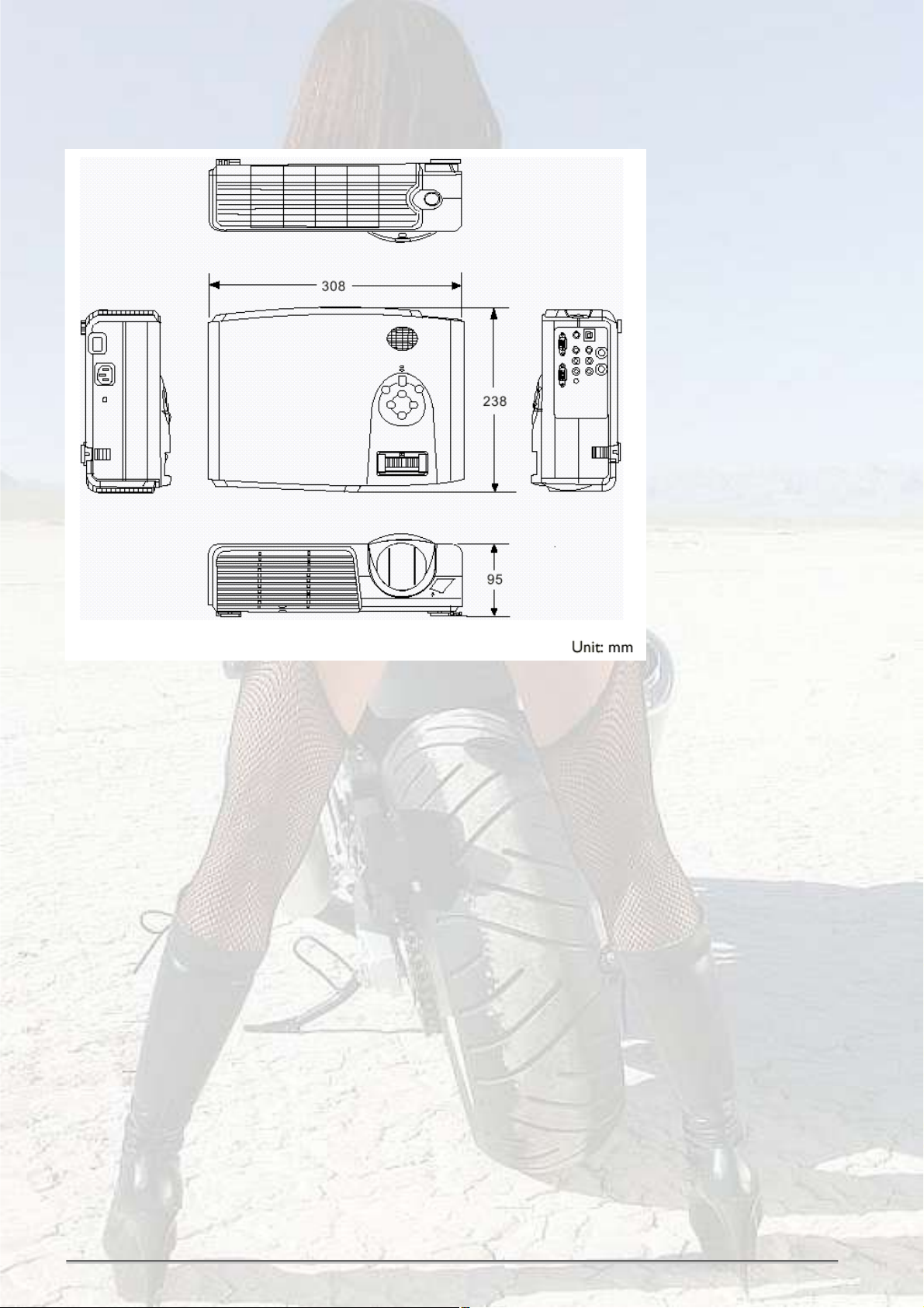
18. Dimensions
49
Page 50

5
D D
4
3
2
1
DMDVCC
VBIAS
VCC2
DMDMODE0
DMDMODE1
COMP
LOADZ
LOAD16
LSET
SCA_BUS
UROWENZ
DMD_DCLK
C C
DMDACLK
CWCTR
CWY3
CWY2
CWY1
OPDIODE
CWSPEED
DD[5:57]
MBRST8
MBRST4
MBRST5
MBRST6
MBRST0
MBRST1
02_80Pin_CONN*2
B B
80Pin_CONN*2
MBRST0
MBR ST1
MBRST7
MBRST2
MBRST3
MBRST2
MBRST3
MBRS T9
MBRS T12
MBR ST11
MBRST14
MBRST13
MBRST10
MBRST7
MBR ST6
MBR ST4
MBRST5
MBRST8
MBRST9
MBRST10
MBRST11
MBRST12
MBRST13
MBRST14
DMDVCC
VBIAS
VCC2
DMDMODE0
DMDMODE1
COMP
LOADZ
LOAD16
LSET
SCA_BUS
UROWENZ
DMD_DCLK
DMDACLK
CWCTR
CWY3
CWY2
CWY1
OPDIODE
CWSPEED
DD[5:57]
MBRST[0:14]
XGA_DMD
DMDVCC
VBIAS
VCC2
DMDMODE0
DMDMODE1
COMP
LOADZ
LOAD16
LSET
SCA_BUS
UROWENZ
DMD_DCLK
DMDACLK
CWCTR
CWY3
CWY2
CWY1
OPDIODE
CWSPEED
DD[5:57]
03_DMD
MBRST[0:14]
A A
Project Code
Title
DS660 DMD CHIP BD
SizeDocument Number Rev
304-C01
A3
Date: Sheet of
5
4
3
2
ANGEL HU
99.J3877.001
48.J3802.S01 FAB:S01
Reviewed By Approved ByPrepared By
BILL WJ CHANG
1
0
14Monday, March 25, 2002
T.S.WU
Page 51

5
D D
4
3
2
1
DD[5:57]
CWY3
CWY2
CWY1
CWCT R
CWCTR
C C
OPDIODE
CWY3
CWY2
CWY1
OPDIODE
1357911131517192123252729313335373941434547495153555759616365676971737577
VCC2
MBRST8
MBRST4
MBRST5
MBRST6
MBRST7
MBRST0
MBRST1
MBRST2
CWSPEE D
VCC2
MBRST5
MBRST8
MBRST6
MBRST7
CWSPEED
MBRST4DMDMODE1
MBRST3
DD27
DD25
DD17
DD19
DD10
DD11
DD6
DD8
MBRST0
MBRST3
MBRST2
MBRST1
DD20
79
DD23
DD22
J9
1357911131517192123252729313335373941434547495153555759616365676971737577
DD39
DD26
DD36
DD42
DD40
DD55
DD52
DD46
DD54
DD53
DD48
DMDVCC
DD57
DD56
DMDVCC
79
J8
24681012141618202224262830323436384042444648505254565860626466687072747678
LOAD16
DMDACLK
VBIAS
B B
VBIAS
LOAD16
DMDACL K
LSET
LOADZ
SCA_BUS
UROWENZ
LOADZ
SCA_BUS
UROW ENZ
DMDMODE0
MBRST14
DMD_DCLK
LSET
MBRST14
DMD_DC LK
DMDMODE 1
DMDMODE 0
MBRST9
MBRST10
COMP
MBRST11
MBRST12
MBRST13
MBRST12
MBRST11
MBRST13
MBRST10
DD5
COMP
MBRST9
80
DD12
DD13
DD7
DD9
24681012141618202224262830323436384042444648505254565860626466687072747678
DD18
DD16
DD15
DD14
DD28
DD30
DD21
DD24
DD33
DD32
DD31
DD29
DD37
DD41
DD34
DD38
DD35
DD50
DD43
DD44
DD49
DD47
DD45
80
DD51
DMDVCC
A A
Project Code
Title
DS660 DMD CHIP BD
SizeDocument Number Rev
304-C01
A3
Date: Sheet of
5
4
3
2
ANGEL HU
99.J3877.001
48.J3802.S01 FAB:S01
Reviewed By Approved ByPrepared By
BILL WJ CHANG
1
0
24Monday, March 25, 2002
T.S.WU
Page 52

5
4
3
2
1
J1
4
D D
3
2
1
CWY3
CWY2
CWY1
CWCTR
CON_4P_S
J2
3
2
1
CON_3P_S
CWSPEED
OPDIODE
DD[5:57]
DD[5:57]
DMDVCC
DD12
DD10
DD13
DD9
DD5
DD8
DD6
DD7
C57
D56
C55
C53
D52
C51
D50
C49
D48
U3
D0D1D2D3D4D5D6D7D8
D52
D51
D50
D49
D48
D2C3D4C5D6C7D8C9D10
DMD_DCLK
COMP
LSET
DMDVCC
LOADZ
SCA_BUS
VBIAS
MBRST[0:14]
MBRST14
MBRST13
MBRST12
MBRST11
MBRST10
MBRST9
MBRST8
MBRST7
MBRST6
MBRST5
MBRST4
MBRST3
MBRST2
MBRST1
MBRST0
DMDDCLK
COMP
LSET
DMDVCC
LOADZ
SCA_BUS
VBIAS
R9610K
c115
4.7U
50V Z
B11
B13
B15
B17
B19
A20
B21
A22
B23
A24
A26
B27
A28
A44
A46
A48
A50-
A52
B45
B57
A56
B51
A54
A40
B29
B7
B9
B1
A4
A2
MBRST14
MBRST13
MBRST12
MBRST11
MBRST10
MBRST9
MBRST8
MBRST7
MBRST6
MBRST5
MBRST4
MBRST3
MBRST2
MBRST1
MBRST0
GND
GND
GND
GND
GND
DCLK
COMP
LSET
DSEL_0
DSEL_1
LOADB
RE_WEB
SAC_BUS
SDOUT
SHIELD
C C
B B
MBRST[0:14]
C47
D9
D47
D46
D45
D44
D43
D42
C11
D12
DD20
DD15
DD17
DD22
DD1 8
DD2 3
DD21
DD16
D46
C45
D44
C43
D42
C41
D40
C39
D38
D10
D11
D12
D13
D14
D15
D16
D17
D18
D41
D40
D39
D38
D37
D36
D35
D34
D33
C13
D14
C15
D16
C17
D18
C19
D20
C21
DD19
DD14
DD11
DD29
DD27
DD26
DD24
DD28
DD30
DD25
C37
D36
C35
D34
C33
D32
C31
D19
D20
D21
D22
D23
D24
D25
A9
A8
A7
A6
A5
A4
A3
A2
A1
A0
LOAD_B
ROWENB
ACLK
MODE0
MODE1
VCC2A
VCC2B
VCC2C
VCC2D
VCC2E
VCC2F
VCCA
VCCB
VCCC
VCCD
GND
GND
GND
GND
GND
GND
D32
D31
D30
D29
D28
D27
D26
D22
C23
D24
C25
C27
C29
D30
A18
B25
B31
B33
A34
B35
A36
B37
A38
B47
B49
B43
B39
A42
A41
B3
B5
B53
B55
C1
D54
A30
A32
D26
D28
A6
A8
A10
A12
A14
A16
R1
560
C111
.047U
50V K
C113
.047U
50V K
C112
.047U
50V K
LOAD16
UROWENZ
DMDACLK
DMDMODE0
DMDMODE1
VCC2
C114
.047U
50V K
DMDVCC
LOAD16
UROWENZ
DMDACLK
DMDMODE0
DMDMODE1
VCC2
DMDVCC
DD57
DD56
DD55
DD54
DD53
DD52
DD51
DD50
DD49
DD48
DD47
DD46
DD45
DD44
DD43
DD42
DD41
DD40
DD39
DD38
DD37
DD36
DD35
DD34
DD33
DD32
DD31
A A
5
4
DD[5:57]
DD[5:57]
Project Code
Title
DS660 DMD CHIP BD
SizeDocument Number Rev
304-C01
A3
Date: Sheet of
3
2
ANGEL HU
99.J3877.001
48.J3802.S01 FAB:S01
Reviewed By Approved ByPrepared By
BILL WJ CHANG
1
0
34Monday, March 25, 2002
T.S.WU
Page 53

5
D D
4
3
2
1
Screw Holes
C C
1
5
4
3
2
9
8
7
6
H1
HOLE-V8
B B
A A
5
5
4
3
2
H2
HOLE-V8
1
9
8
7
6
1
5
4
3
2
9
8
7
6
H3
HOLE-V8
4
5
4
3
2
H4
HOLE-V8
1
9
8
7
6
3
Ñ°¬·½¿´ б·²¬-
OP1
OP
OP8
OP
2
OP3
OP
OP10
OP
OP4
OP
OP11
OP
OP5
OP
OP12OPOP13
OP
OP2
OP
OP9
OP
Project Code
Title
DS660 DMD CHIP BD
SizeDocument Number Rev
304-C01
A3
Date: Sheet of
ANGEL HU
OP7
OP6
OP
OP
OP14
OP
99.J3877.001
48.J3802.S01 FAB:S01
Reviewed By Approved ByPrepared By
BILL WJ CHANG
1
0
44Monday, March 25, 2002
T.S.WU
Page 54

Page 55

Page 56

Page 57

5
4
3
2
1
VDD
VDD
J1
RN1
LED0
LED0
LED1
LED1
LED2
LED2
LED3
KEY[6:0]
LED3
KEY[6:0]
D D
C C
5
6
7
8
KEY0
KEY1
KEY2
KEY3
KEY4
KEY5
KEY6
4
3
2
1
47
VDD
R17150
R19150
B B
R23150
R26150
R28150
R30150
LED1GREEN
1 2
LED3GREEN
1 2
LED5GREEN
1 2
LED7GREEN
1 2
LED9GREEN
1 2
LED11GREEN
1 2
GND
1
2
3
4
5
6
7
8
9
10
11
12
13
14
15
GND
KEY[6:0]
VDD
R18150
R20150
R24150
R27150
R29150
R31150
VDD
R5
2K
KEY0
KEY1
KEY2
KEY3
KEY4
KEY5
KEY6
LED2GREEN
1 2
LED4GREEN
1 2
LED6GREEN
1 2
LED8GREEN
1 2
LED10GREEN
1 2
LED12GREEN
1 2
SW1
LED2
1 3
2 45
C1680P
50V J
50V J
50V J
50V J
SW2
1 3
2 45
C2680P
50V J
12V
SW4
1 3
2 45
C4680P
50V J
12V
SW6
1 3
2 45
C6680P
12V
50V J
LED3
LED0
LED1
12V
R9
R8
R7
R6
2K
2K
2K
2K
R10
2K
R11
2K
SW3
1 3
2 45
C3680P
12V
SW5
1 3
2 45
C5680P
12V
SW7
1 3
2 45
C7680P
12V
VDD
VDD
VDD
R1
R12
R15
10K
R3
2K
10K
R13
2K
10K
R22
R16
2K
10K
R25
2K
LED2A
LED3A
LED0A
LED1A
R2
150
32
Q1
1
2N3904
D1
4 2
3
1
YL/GN
R4
150
32
Q2
1
2N3904
R14
150
D2
1 2
32
RED
Q3
1
2N3904
R21
D3
150
1 2
32
1
Q4
2N3904
RED
GND
A A
Project Code
Title
SizeDocument Number Rev
304-C01
A3
Date: Sheet of
5
4
3
2
ANGEL HU
99.J2077.001
DX660 KEYPAD BD SCHEMAICS
48.J3403.S01
Reviewed By Approved ByPrepared By
BILL WJ CHANG H.C.TSOU
1
12Saturday, March 02, 2002
FAB:S01
0
Page 58

5
4
3
2
1
Ñ°¬·½¿´ б·²¬-
OP1
OP
D D
OP8
OP
OP2
OP
OP9
OP
OP3
OP
OP10
OP
OP4
OP
OP11
OP
OP5
OP
OP12
OP
OP6
OP
OP13
OP
OP7
OP
OP14
OP
Screw Holes
C C
5
4
3
2
9
8
7
6
H1
HOLE-V8
B B
5
4
3
2
H2
HOLE-V8
9
8
7
6
5
4
3
2
9
8
7
6
H3
HOLE-V8
5
4
3
2
H4
HOLE-V8
9
8
7
6
GND
Project Code
Title
A A
Size Document Number Rev
A3
DX660 KEYPAD BD SCHEMAICS
304-C01
Date: Sheet of
99.J2077.001
48.J3403.S01
FAB:S01
22Saturday, March 02, 2002
0
Reviewed By Approved ByPrepared By
5
4
3
2
ANGEL HU
BILL WJ CHANG H.C.TSOU
1
Page 59

A
Page_3 03_DOUT
VDD
VDD
GND
VSYNC_O
GAIN_B
RAIN_B
BAIN_B
HSYNC_O
RAIN_B
4 4
GAIN_B
BAIN_B
VDD
B
VDD
3.3V
VDD
3.3V
SDA_M
SCL_M
ROMW En
ROMO En
VPPEN
EEP_WP
C
Page_6
06_MEMORY
A[19:1]
D[0:15]
A[19:1]
D[0 :15]
D
Page_8
08_MISC
GND
DCKEXT
MCKEXT
WATCHDOG
RESET
DCKEXT
MCKEXT
GND
POWERON
VDD
3.3V
VDD
3.3V
E
3.3V
VDD
V12
HSY NC_ O
VSYN C_O
VVS
VFIELD
VPEN
VHS
VCLK
GRE[7:0]
GGE[7:0]
GBE[7:0]
GHS
GVS
GBLKSPL
GFBK
GCLK
GCOAST
PC_YP_SW
RXD
TXD
REMOTE_IR
VY[7:0]
VUV[7:0]
VDD
VY[7:0]
VUV[7:0]
VVS
VFIELD
VPEN
VHS
VCLK
GPENSOG
GRO[7:0]
GRE[7:0]
GGO[7:0]
GGE[7:0]
GBO[7:0]
GBE[7:0]
GHS
GVS
GBLKSPL
GFBK
GCLK
GCOAST
PC_YP_SW
ROMO En
GND
RXD
TXD
AUDIO_R
AUDIO_L
PC_AUDIO_L
PC_AUDIO_R
Page_10
10_AUDIO_&_DETECT
A[19:1]
VPPEN
ROMWEn
D[0:15]
EEP_WP
WATCHDOG
Page_7
07_PW166
LED[3:0]
LED [3:0]
LED[3:0]
GND
C
A0
HSYNC
VSYNC
Yp/Yc
Pb/Cb
Pr/Cr
CVBS
LUMA
CHROMA
CVBS
LUMA
CHROMA
LLC1
LLC2
GND
Page_4
04_DECODE
RAIN_B
GAIN_B
BAIN_B
HSYNC
VSYNC
Yp/Yc
Pb/Cb
Pr/Cr
GND
Page_5
05_AFE
VY[7:0]
VDD
VUV[7:0]
VVS
VFILD
VPEN
VHS
VCLK
SCL
SDA
V33
V33
GRE[7:0]
V33
SCL
SDA
GGE[7:0]
GBE[7:0]
GHS
GVS
GBLKSPL
GFBK
GCLK
GCOAST
PC_YP_SW
VDD
CVBS
LUMA
BAIN_B
RAIN_B
GAIN_B
CHROMA
VSYN C_O
HSYN C_O
3 3
HSYNC
VSYNC
Yp/Yc
Pb/Cb
Pr/Cr
PC_YP_SW
VDD
2 2
Page_2
02_INPUT
AUDIO_R
AUDIO_L
PC_AUDIO_L
PC_AUDIO_R
GND
1 1
Page1
RXD
VDD
TXD
GND
PAGE1
A
Page_11
11_USB
GND
REMOTE_IR
AUDIO_R
AUDIO_L
PC_AUDIO_L
PC_AUDIO_R
B
RESET
POWERON
TDI
NMI
TCK
TMS
TDO
RESET
BHENn
DCKEXT
MCKEX T
RESETZ
DRO[7:0]
DRE[7:0]
DGO[7:0]
DGE[7:0]
DBO[7:0]
DBE[7:0]
DHS
DVS
DEN
POWERON
RESETZ
DRE[7:0]
DGE[7:0]
DBE[7:0]
DCLK
IRRCVR
VDD 3.3V
VDD
3.3V
SDA
SCL
LAMPLITZ
SDA
ALERT
LOW_P
AUDIO _MUT
CS0n
ALERT
CS0n
LOW_P
AUDIO_MUT
CS0n
ALERT
LOW_ P
AUDIO_MU T
VDD
V12
3.3V
VDD
V12
SCL
SCL
SDA
D[0:7]
3.3V
D
LAMPLITZ
ProjectCode
99.J3477.001
Title
Size Document Number Rev.
PCB P/N
<Size>
48.J3402.S03
Tuesday, May 21, 2002
Date: Sheet of
Model Name
MAIN BD
ANGEL HU
Page_9
09_DISPLAY
RESETZ
DX660
PCBRev.
S03
Reviewed By ApprovedByPrepared By
BILL WJCHANG
POWERON
RESETZ
DRE[7:0]
DGE[7:0]
DBE[7:0]
DHS
DVS
DEN
DCLK
IRRCVR
SDA_M
SCL_M
SDA
SCL
LAMPLITZ
E
V12
3.3V
VDD
CWINDEX
GND
LAMPE NA
LAMPLI T
LAMPLIT
LAMPENA
LAMPLIT
LAMPENA
OEM/ODM Model Name
NA
304-C02
112
T.S.WU
1
Page 60

A
VDD VDD
2
DN2
4 4
L3
1617
11
12
13
14
15
3 3
6
1
7
2
8
3
9
4
10
5
2024012015
RED_GND
RIN_1
GREEN_GND
GIN_1
BLUE_GND
BIN_1
PC_5VIN
VDD
2
VDD
R7
R8
2
3
BAV99
BAV99
1
1
DN6
DN7
BAV99
1
0
0
3
VDD
2
1
DN3
3
BAV99
3
VDD
D5
GSDA
5.1V
1 2
GSCL
B
2
DN4
3
BAV99
1
1 2
D1 1N4148
1 2
D2 1N4148
1 2
D3 5.1V
1 2
D4 5.1V
U2
5
SDA
6
SCL
7
WP
8
VCC
AT24C02A
R9 4.7K
R12 4.7K
4
VSS
3
A2
2
A1
1
A0
DDC5V
C1
0.1U
25V Z
RV1
47
RH1
47
C
1
R1
R2
R3
R4 75
R5 75
R6 75
47
47
47
RAIN_B
GAIN_B
BAIN_B
RAIN_B
GAIN_B
BAIN_B
2
VCC
OE2
OE3
VDD
14
3
O0
6
O1
11
O2
8
O3
13
10
R1447
R1547
HSYNC
HSYNC_O
VSYNC
VSYNC_O
PC_YP_SW
HSYNC
HSYNC_O
VSYNC
VSYNC_O
PC_YP_SW
4
6
U1
7
GND
2
A0
5
A1
12
A2
9
A3
1
OE0
4
OE1
74AHC125
GND
L1
BEAD
334
1
J2
2
4
6
2210019011
J1
556
D
VDD
6
1
3
5
4
2
2
1
3
5
3
2
DN1 BAV99
L2
BEAD
VDD
L4 BEAD
L5 BEAD
L6 BEAD
1
2
3
DN5BAV99
2
DN8
3
3
BAV99
1
2
1
R10 18
R11 18
R13 18
2
DN9
3
BAV99
1
3
1
CV10
0.1U M
25V
2
DN10
BAV99
1
VDD
CV11
0.1U M
25V
R16
56
E
CHROMA
R17
56
R18
56
LUMA
Pr/Cr
Pb/Cb
Yp/Yc
CHROMA
LUMA
Pr/Cr
Pb/Cb
Yp/Yc
DN11BAV99
R19
R21
3
C9
47P
50V J
VDD
CVBS
2
DN15
BAV99
1
CV12
0.1U M
AUDIO_L
0
AUDIO_R
0
2
DN16
3
BAV99
1
J3
J4
1
2 2
3
5
4
2
1
3
5
4
2
L9 BEAD
L11 BEAD
2210185001
25V Z
C30.1U
25V Z
C50.1U
C6
47P
50V J
2
DN12
3
BAV99
C7
47P
1
50V J
R20
0
PC_AUDIO_R
R22
0
PC_AUDIO_L
VDD
2
DN13
3
BAV99
1
VDD
VDD
PC_AUDIO_R
PC_AUDIO_L
2
4
6
2
4
6
2210019011
1
3
5
BEAD
L7
1
BEAD
L8
3
BEAD
L10
5
25V Z
25V Z
C20.1U
C40.1U
2
DN14
3
BAV99
C8
47P
1
50V J
CVBS
25V
AUDIO_L
AUDIO_R
VDD
ProjectCode
1 1
A
B
C
D
99.J3477.001
Title
Size Document Number Rev.
PCB P/N
<Size>
48.J3402.S03
Tuesday,May 21, 2002
Date: Sheet of
ANGEL HU
Model Name
MAIN BD
DX660
PCBRev.
S03
Reviewed By ApprovedByPrepared By
BILL WJCHANG
OEM/ODM Model Name
304-C02
212
E
NA
1
T.S.WU
Page 61

A
B
C
D
E
L13
2024012015
16 17
5
10
4
9
3
8
2
7
1
6
BLUE_OUT
GREEN_OUT
RED_OUT
DN19
BAV99
R26 75
R27 75
2
3
1
DN20
BAV99
2
DN21
3
3
BAV99
1
VDD
2
1
RGBO_BH_OUT
RGBO_G
RGBO_R
RGBO_B
RGBO_G
RGBO_R
4 4
VSYNC_O
HSYNC_O
VSYNC_O
HSYNC_O
R23 47
R24 47 R25 75
V_OUT
14
13
12
VDD
11
2
2
DN18
15
DN17
BAV99
3 3
3
3
BAV99
1
1
VDD
-5V_PIN1
R31 0
U4
1
NC
2
CAP+
3
GND
CAP-4VOUT
ICL7660S 5V
OSC
C13
25V Z
õ
C16
25V
1 2
22U
0.1U
-5V
C18
25V Z
-5V
0.1U
GND
8
V+
7
6
LV
5
C17
0.1U
25V Z
VDD
C14
0.1U
25V Z
RAIN_B
2 2
RGBO_R
RAIN_B
RGBO_R
R34
R35
820
820
IN1- IN3-
1
2
3
4
5
6
7
U3
DIS1
DIS2
DIS3
+VS
+IN1
-IN1
OUT1
AD8013
OUT2
-IN2
+IN2
-VS
+IN3
-IN3
OUT3
14
IN2-
13
R32
R33
820
820
12
11
10
820
9
8
R37
R36
820
GAIN_B
-5V
BAIN_B
RGBO_G
RGBO_B
RGBO_G
GAIN_B
-5V
BAIN_B
RGBO_B
12
C15
10U 25V
CAP+
õ
CAP-
ProjectCode
1 1
A
B
C
D
99.J3477.001
Title
Size Document Number Rev.
PCB P/N
<Size>
48.J3402.S03
Tuesday,May 21, 2002
Date: Sheet of
ANGEL HU
Model Name
MAIN BD
DX660
PCBRev.
S03
Reviewed By ApprovedByPrepared By
BILL WJCHANG
OEM/ODM Model Name
304-C02
312
E
NA
1
T.S.WU
Page 62

A
B
C
D
E
B12
TEST5
VDDD1C5VDDD3C9VDDD5
DECOE
P12
P11
A12
A13
M12
TEST1
TEST2
TEST3B2TEST4
AMCLK
ALRCLK
AMXCLK
VDDD7
VDDD9M4VDDD11M8VDDD13
VSS(xtal)A4VDD(xtal)B3XTOUTA2XTALOA3XTALIB4ADP8P6ADP7M6ADP6L6ADP5N7ADP4P7ADP3L7ADP2M7ADP1
D12
H12
M11
R38
LLC2
LLC1
10K
LLC2
LLC1
XRI
B11
P4
N5
M10
N10
L10
P5CEN4
P9
N9
P10
N11
SCL
SDA
INT_A
ASCLK
LLC
RES
XTRI
LLC2
RTS0
RTS1
RTCO
D8
XRV
C7
XRH
A6
XRDY
B7
XDQ
A7
XCLK
A8
XPD0
B8
XPD1
A9
XPD2
B9
XPD3
A10
XPD4
B10
XPD5
A11
XPD6
C11
XPD7
HPD0
HPD1
HPD2
HPD3
HPD4
HPD5
HPD6
HPD7
IGP1
IGP0
IGPV
IGPH
ITRDY
ICLK
IPD0
IPD1
IPD2
IPD3
IPD4
IPD5
IPD6
IPD7
CLKEXT
ADP0
ITRI
IDQ
D14
E11
E13
E12
E14
F13
F14
G13
L12
K13
L14
K14
K12
N12
L13
M14
G14
G12
H11
H14
H13
J14
J13
K11
N6
N8
VUV0
VUV1
VUV2
VUV3
VUV4
VUV5
VUV6
VUV7
ITRI
VCLK_A
VY0
VY1
VY2
VY3
VY4
VY5
VY6
VY7
VDD VAA
C20
0.1U
25V Z
U6LD1117-3.3V
3
VOUT
VIN
GND
1
2
12
õ
C19
22U
25V
VAA VAA VAA VAA VAA VAA VAA VAA VAA
C32
0.1U
25V Z
VUV[7:0]
C33
0.1U
25V Z
R45 0
C34
0.1U
25V Z
C35
0.1U
25V Z
C36
0.1U
25V Z
VFILD
VVS
VHS
VPEN
VCLK
C37
0.1U
25V Z
C38
0.1U
25V Z
VUV[7:0]
VFILD
VVS
VHS
VPEN
VCLK
C39
0.1U
25V Z
R46
10K
VY[7:0]
GND
LLC2
LLC1
VY[7:0]
LLC2
LLC1
C40
0.1U
25V Z
P8
SCL
SDA
4 4
VDD
CVBS
CHROMA
3 3
LUMA
2 2
SCL
SDA
CVBS
CHROMA
LUMA
VDD
C21
0.1U
25V Z
R3918
R4018
R4118
U5
3
VIN
LD1117-3.3V
VOUT
GND
1
R42
R43
56
56
R44
56
2
V33
C22
0.1U
25V Z
RCVBS
RLUM
RCHR
V33
C23
0.1U
25V Z
C31
.047U
50V K
C24
0.1U
25V Z
C30
C41
C42
C43
C44
C45
C25
0.1U
25V Z
.047U
50V K
.047U
50V K
.047U
50V K
.047U
50V K
.047U
50V K
.047U
50V K
VAA
C26
0.1U
25V Z
X200
AI12
AI1D
AI22
AI2D
AI3D
AI4D
C27
0.1U
25V Z
C28
0.1U
25V Z
C29
0.1U
25V Z
M13
B13
B14
C12
C13
C14
D13
N13
N14
P13
D6
B6
C6
B5
A5
TDI
TCK
TMS
TDO
TRST
FSW
J2
AI11
K1
AI12
K2
AI13
L3
AI14
K3
AI1D
C2
AGND
G4
AI21
G3
AI22
H2
AI23
J3
AI24
H1
AI2D
E3
AI31
F2
AI32
F3
AI33
G1
AI34
F1
AI3D
L2
AGNDA
B1
AI41
D2
AI42
D1
AI43
E1
AI44
D3
AI4D
P3
EXMCLR
M1
AOUT
M2
VSSA0
J4
VSSA1
H3
VSSA2
E4
VSSA3
C1
VSSA4
M3
VDDA0
K4
VDDA1
H4
VDDA2
F4
VDDA3
D4
VDDA4
L1
VDDA1A
J1
VDDA2A
G2
VDDA3A
E2
VDDA4A
VSSD2D7VSSD4
D10
TEST18P2TEST19
VSSD6
VSSD8
VSSD10L5VSSD12L9VDDD2C8VDDD4
J11
F11
TEST12
TEST13N1TEST14N2TEST15N3TEST16
TEST17
VDDD6
VDDD8
VDDD10M5VDDD12M9VSSD1D5VSSD3D9VSSD5
J12
F12
C10
TEST6
TEST7C3TEST8C4TEST9
TEST10
TEST11
U7
SAA7118E
VSSD7
VSSD9L4VSSD11L8VSSD13
L11
D11
G11
V33
V33
XTAL
24.576MHZ
Y1
C47
50V J
18P
XTALI
C48
50V J
18P
ProjectCode
99.J3477.001
Title
Size Document Number Rev.
PCB P/N
<Size>
D
48.J3402.S03
Tuesday, May 21, 2002
Date: Sheet of
ANGEL HU
Model Name
MAIN BD
DX660
PCBRev.
S03
Reviewed By ApprovedByPrepared By
BILL WJCHANG
OEM/ODM Model Name
304-C02
412
E
NA
1
T.S.WU
V33
1 1
A
B
12
C46
22U
25V
õ
C
Page 63

A
V33
R50
1KF
U9
14
VCC16CX1
RCX1
CX2
RCX2
GND
74LV123
8
15
13
4
5
12
6
7
1 2
D61N4148
1 2
D321N4148
C257220P
25V K
1Q
1Q
2Q
2Q
1
4 4
GHS1
C258
R152
1U K
390K
<Spec>
1A
2
1B
3
1R
9
2A
10
2B
11
2R
R47 47K
R48
R150
220K
R151
GND
3 3
BAIN
GAIN
RAIN
SCL
SDA
GAIN
RAIN
SCL
SDA
C18110P J
C18210P J
C18310P J
R52
R53
R55
68
68
68
AVDD
50V K
HDD
AVDD
Pr/Cr_I
12
L14 BEAD
VDD
12
U12
1
10
11
12
2
3
4
5
6
7
8
9
RIN_1
HDdetect
GIN_1
GND
BIN_1
GND
RIN_2
GND
GIN_2
GND
BIN_2
VIN_1
Pb/Cb_I
12
12
GAIN_I
12
BA7657F
12
R57470K
C70470P
2 2
C710.01U
Pr/Cr
Yp/Yc
Pb/Cb
RAIN_B
1 1
GAIN_B
BAIN_B
Pr/Cr
Yp/Yc
Pb/Cb
RAIN_B RAIN_I
GAIN_B
BAIN_B
50V K
C7210U M 20V
C730.01U
50V K
C7410U M 20V
C780.01U
50V K
C8510U M 20V
C860.01U
50V K
C8710U M 20V
C880.01U
50V K
C8910U M 20V
C900.01U
50V K
C9110U M 20V
A
360
1KF
GBIN_A
GGIN_A
C671000P
50V K
GRIN_A
HIN_1
DIN_2
HD_O
R_out
VCC
G_out
CON_IN
CON_O
CTL
B_out
VD_out
VIN_2
B
VSYNC
HSYNC
GCOAST
GBLKSPL
C65
C66
C68.047U
AVDD
24
23
22
21
20
19
18
17
16
15
14
13
B
AVDD
50V K
.047U
AVDD
50V K
.047U
AVDD
50V K
C69
0.1U
25V Z
GVREF
R58
68K
GHS
VSYNC
HSYNC
GCOAST
GBLKSPL
PVDD
AVDD
GBINBAIN
AVDD
GGIN
AVDD
GRIN
AVDD
C75
0.01U
50V K
RAIN
GAIN
PC_YP_SW
BAIN
PVDD
PVDD
3900P
39N
C58
50V K
25V K
REF_A
R49
3.3K
GFILT
AVDD
PVDD
32
35
36
37
38VD39
40
FILT33PVD34PVD
GND
GND
41
GND
CLAMP
42
43
44
45
46
47
48
49
50
51
52
53
54
55
56
57
58
59
60
VD
BAIN
GND
VD
VD
GND
GAIN
SOGIN
GND
VD
VD
GND
RAIN
A0
SCL
SDA
REF BYPASS
VD
GND
MIDSCV
U11
AD9883AKST-140
GND61VD62GND63VSOUT64SOGOU T65HSOUT66DATACK67GND68VDD69R770R671R572R473R374R275R176R077VDD78VDD79GND
ADVS
ADSOG
ADHS
C76
1U
16V Z
RN6
47
ADCK
123
4
876
5
R59
RAIN
47
GAIN
PC_YP_SW
BAIN
CN 6
C
VDD
U8LD1117-3.3V
AVDD
1
VOUT
GND
2
12
C51
õ
C50
22U
0.1U
25V
25V Z
VDD VDD
3
VIN
C49
0.1U
C59
25V ZC57390P K
C52
0.1U
25V Z
D
C53
0.1U
25V Z
C54
0.1U
25V Z
V33
V33
GVMID
AVDD
V33
21
23
25VD26VD27
28
29
30
31
VDD22VDD
GND
GND24GND
GND
GND
VSYNC
COAST
HSYNC
GND
VDD
GND
GND
B0
B1
B2
B3
B4
B5
B6
B7
G0
G1
G2
G3
G4
G5
G6
G7
C61
0.1U
25V Z
20
19
18
17
16
15
14
13
12
11
10
9
8
7
6
5
4
3
2
1
ADBE0
ADBE1
ADBE2
ADBE3
ADBE4
ADBE5
ADBE6
ADBE7
ADGE0
ADGE1
ADGE2
ADGE3
ADGE4
ADGE5
ADGE6
ADGE7
RN1
5
6
7
8
V33
RN3
5
6
7
8
12
C77
õ
C79
C80
22U
0.1U
25V
47
4
3
2
RN2
1
5
6
7
8
47
4
3
2
RN4
1
5
6
7
8
47
0.1U
25V Z
25V Z
6 3
5 4
47
4
3
2
1
4
3
2
1
817263
CN 2
80
ADRE0
ADRE2
ADRE3
ADRE4
ADRE1
ADRE5
ADRE6
ADRE7
V33
817263
V33
RN747
V33
1
2
3
4
GCLK
GFBK
GHS1
GVS
54
22P
C
8
7
6
5
1
2
3
4
GCLK
GFBK
GHS1
GVS
GRE0
GRE1
GRE2
GRE3
RN547
GRE4
8
GRE5
7
GRE6
6
GRE7
5
817263
CN7
54
817263
22P
CN8
D
E
VDD PVDDAVDD
U10LD1117-3.3V
PVDD
3
VIN
C55
0.1U
25V Z
C81
0.1U
25V Z
7 2
8 1
C56
0.1U
25V Z
CN4
22P
54
C82
0.1U
25V Z
22P
C83
0.1U
25V Z
5 4
817263
CN3
C62
0.1U
25V Z
C84
0.1U
25V Z
CN5
22P
8 1
7 2
6 3
GBE0
GBE1
GBE2
GBE3
GBE4
GBE5
GBE6
GBE7
GGE0
GGE1
GGE2
GGE3
GGE4
GGE5
GGE6
GGE7
54
22P
GRE[7:0]
54
22P
ProjectCode
99.J3477.001
Title
Size Document Number Rev.
PCB P/N
<Size>
48.J3402.S03
Tuesday, May 21, 2002
Date: Sheet of
Model Name
MAIN BD
ANGEL HU
2
VOUT
GND
1
GBE[7:0]
GGE[7:0]
GRE[7:0]
DX660
PCBRev.
S03
Reviewed By ApprovedByPrepared By
BILL WJCHANG
12
C60
C63
õ
0.1U
22U
25V Z
25V
GBE[7:0]
GGE[7:0]
OEM/ODM Model Name
304-C02
512
E
NA
C64
0.1U
25V Z
T.S.WU
1
Page 64

A
B
C
D
E
A[19:1]
A16
1
2
3
4
5
6
7
8
9
10
11
12
13
14
15
16
17
18
19
20
21
22
23
24
A15
A14
A13
A12
A11
A10
A9
A8
A19
NC
WE#
RESET#
NC
NC
RY/BY#
A18
A17
MBM29LV400TC
A7
A6
A5
A4
A3
A2
A1
A15
A14
A13
A12
A11
A10
A9
VPP3.3V
A19
A18
A8
A7
A6
A5
A4
A3
A2 A1
U13
A16
BYTE#
VSS
DQ15/A-1
DQ7
DQ14
DQ6
DQ13
DQ5
DQ12
DQ4
VCC
DQ11
DQ3
DQ10
DQ2
DQ9
DQ1
DQ8
DQ0
OE#
VSS
CE#
A0
32
R63
1K
2N3904
R61
3.3K
3.3V
C92
0.1U
25V Z
ROMWPn
3.3V
R62
1K
3.3V
4 4
3.3V
R60 1M
3.3V
ROMWEn
VPPEN
3 3
ROMWEn
3.3V
VPPEN VPPON VP1
R641M Q2
R6510K
R66
3.3K
Q1
2N3906
1
VP3
VP2
32
1
A17
48
47
3.3V
46
D15
45
D7
44
D14
43
D6
42
D13
41
D5
40
D12
39
D4
38
37
3.3V
D11
36
D3
35
D10
34
D2
33
D9
32
D1
31
D8
30
D0
29
28
27
26
25
D[0:15]
ROMOEn
D[0:15]
ROMOEn
R67
3.3K
2 2
VDD
GND
VDD
SCL_M
SDA_M
R68
2K
32
Q3
1
EEP_WP
2N3904
ProjectCode
99.J3477.001
Title
Size Document Number Rev.
PCB P/N
<Size>
C
D
48.J3402.S03
Tuesday, May 21, 2002
Date: Sheet of
ANGEL HU
Model Name
MAIN BD
DX660
PCBRev.
S03
Reviewed By ApprovedByPrepared By
BILL WJCHANG
OEM/ODM Model Name
304-C02
612
E
NA
1
T.S.WU
C93
SCL_M
SDA_M
0.1U
25V Z
U14
1
NC
2
NC
3
NC
GND4SDA
AT24C16 16K
1 1
A
B
VCC
WP
SCL
8
7
6
5
Page 65

A
GFBK
VCC6
GND5
GRE0
GRE1
GRE2
GRE3
GRE4
GRE5
GRE6
GRE7
GGE0
GGE1
GGE2
GGE3
GGE4
GGE5
GGE6
GGE7
GBE0
GBE1
GBE2
GBE3
GBE4
GBE5
GBE6
GBE7
K18
VCC7
GND6
D14
GRO0
GRO1
GRO2
GRO3
GRO4
GRO5
GRO6
GRO7
GGO0
GGO1
GGO2
GGO3
GGO4
GGO5
GGO6
GGO7
GBO0
GBO1
GBO2
GBO3
GBO4
GBO5
GBO6
GBO7
R8227
P18
VCC8
GND7
D17
H19
GCLK
V25P
G20
G19
M20
N19
N18
N17
N20
P20
P19
R20
F18
E19
E20
H20
K19
D16
A18
C17
B18
A19
B19
A20
D18
K20
L17
L18
L19
L20
M18
M17
M19
E17
C19
B20
C20
E18
F17
D19
D20
B15
A16
C15
D15
B16
A17
C16
B17
J17
J18
J19
J20
GPENSOG
GVS
GHS
GRE0
GRE1
GRE2
GRE3
GRE4
GRE5
GRE6
GRE7
GGE0
GGE1
GGE2
GGE3
GGE4
GGE5
GGE6
GGE7
GBE0
GBE1
GBE2
GBE3
GBE4
GBE5
GBE6
GBE7
GRO0
GRO1
GRO2
GRO3
GRO4
GRO5
GRO6
GRO7
GGO0
GGO1
GGO2
GGO3
GGO4
GGO5
GGO6
GGO7
GBO0
GBO1
GBO2
GBO3
GBO4
GBO5
GBO6
GBO7
U15A
PW166-10TK
GraphicsPort
3.3V
GFBK
GREF
GBLKSPL
GCOAST
L15
BEAD
V3P
H17
H18
F19
F20
VCLK
VPEN
VVS
VHS
VFIELD
VY[7:0]
VUV[7:0]
V3P
3.3V
C18
U20
V18
Y17
V12
V3
V14
Y14
V11
G3
VDD1C7VDD2
VDD3
VCC9
VCC10
VCC11
VCC12V7VCC13L3VCC14
U15EPW166-10TK
GND8
GND9
GND10
GND11
GND12
GND13
GND14
T19
K17
P17
U17
G17
U14
W17
VDD4
Power and Ground
GND15
GND16
GND17
GND18U9GND19U7GND20W6GND21W4GND22U4GND23L4GND24K4GND25
U12
U11
W14
K3
VDD5
VDD6
VDD7V9VDD8Y6VDD9
VDD10
G4
V3P
GCLK
GPENSOG
GVS
4 4
GRE[7:0]
GGE[7:0]
GBE[7:0]
3 3
GRO[7:0]
GGO[7:0]
GBO[7:0]
2 2
V25
C14
C10
C11
B12
G18
VCC5
VCC1C3VCC2
VCC3
VCC4
1 1
GND1D4GND2D7GND3
GND4
B11
A12
D10
GND
A
GBLKSPLGHS
GCOAST
12
õ
C96
22U
25V
C102
0.1U
25V Z
C112
0.1U
25V Z
VY0
VY1
VY2
VY3
VY4
VY5
VY6
VY7
VUV0
VUV1
VUV2
VUV3
VUV4
VUV5
VUV6
VUV7
V3P
V3PV3P
B
C103
0.1U
25V Z
C113
0.1U
25V Z
B
V25
X700
X701
D12
VCLK
C13
VPEN
A14
VVS
B14
VHS
A15
VFIELD
D8
VY0
C8
VY1
B7
VY2
A7
VY3
B8
VY4
D9
VY5
C9
VY6
A8
VY7
B9
VUV0
A9
VUV1
B10
VUV2
A10
VUV3
D11
VUV4
A11
VUV5
C12
VUV6
B13
VUV7
V3P V3P
C98
0.1U
25V Z
V3P
C104
0.1U
25V Z
C114
0.1U
25V Z
RX1
1M
RX2
1M
SDA
SCL
AUDIO_MUT
LOW_P
ALERT
LAMPLITZ
PC_YP_SW
WATCHDOG
V3P
V3PV3P
U15B
PW166-10TK
Video Port
C99
0.1U
25V Z
C105
0.1U
25V Z
C115
0.1U
25V Z
3.3V
3.3V
R74
R73
2K
2K
AUDIO_MUT
LOW_P
ALERT
LAMPLITZ
PC_YP_SW
WATCHDOG
POWERON
RESETZ
EEP_WP
VPPEN
V25
C106
0.1U
25V Z
V25 V25
C116
0.1U
25V Z
RESET
MCKEXT
DCKEXT
RXD
TXD
IRRCVR
SDA
SCL
R75 47
R76
POWERON
RESETZ
EEP_WP
VPPEN
LED[3:0]
TMS
TCK
TDI
V3P
TDO
R77 4.7K
R78 4.7K
R79 1M
R81 4.7K
V25
12
õ
C97
22U
25V
V25 V25V25
C107
0.1U
25V Z
C117
0.1U
25V Z
C108
0.1U
25V Z
C118
0.1U
25V Z
2K
RN13
5
6
7
8
V25
RN15
C109
0.1U
25V Z
C119
0.1U
25V Z
C
X700
X701
AUDIO_MUTA
LOW_PA
5
6
7
8
4
3
2
1
47
V25 V25
C100
0.1U
25V Z
V25V25
C110
0.1U
25V Z
V25V25
C120
0.1U
25V Z
C
X702
X703
X704
47
LED0
LED1
LED2
LED3
D
W12
DCLK
DRE0
DRE1
DRE2
DRE3
DRE4
DRE5
DRE6
DRE7
DGE0
DGE1
DGE2
DGE3
DGE4
DGE5
DGE6
DGE7
DRO0
DRO1
DRO2
DRO3
DRO4
DRO5
DRO6
DRO7
DGO0
DGO1
DGO2
DGO3
DGO4
DGO5
DGO6
DGO7
DBO0
DBO1
DBO2
DBO3
DBO4
DBO5
DBO6
DBO7
BC2
4.7U
50V Z
DBE0
DBE1
DBE2
DBE3
DBE4
DBE5
DBE6
DBE7
DVS
DHS
DEN
Model Name
MAIN BD
V13
U13
Y15
R19
T20
R18
R17
T18
U19
T17
V20
U18
V19
W20
W19
Y20
V17
U16
W18
Y19
Y18
V16
U15
Y16
V15
W16
W15
Y12
W11
Y11
U10
V10
W10
Y10
W9
Y9
W8
V8
U8
Y8
Y7
W7
Y5
V6
U6
W5
Y4
V5
Y3
V4
Y2
U16
3
VIN
LM317M
PCBRev.
Reviewed By ApprovedByPrepared By
BILL WJCHANG
P1
A0
U15D
PW166-10TK
Misc
ROMOE
ROMWE
RAMOE
RAMWE
EXTINT
ð
ÒÑ
ÒÑ
ð
ð
мтйХмтйХ
ð
ÒÑÒÑ
A10
A11
A12
A13
A14
A15
A16
A17
A18
A19
D10
D11
D12
D13
D14
D15
WR
BHEN
CS0
CS1
NMI
RD
A1
A2
A3
A4
A5
A6
A7
A8
A9
D0
D1
D2
D3
D4
D5
D6
D7
D8
D9
ìòéÕ
E3
RESET
W13
MCKEXT
Y13
DCKEXT
P3
XTALI
P4
XTALO
C1
RXD
D3
TXD
E4
IRRCVR0
D2
IRRCVR1
C2
PORTA0
B1
PORTA1
B2
PORTA2
A1
PORTA3
C4
4
3
2
1
D13
A13
PORTA4
D5
PORTA5
B3
PORTA6
A2
PORTA7
A3
PORTB0
C5
PORTB1
D6
PORTB2
B4
PORTB3
A4
PORTB4
C6
PORTB5
B5
PORTB6
A5
PORTB7
CPUTMS
A6
CPUTCK
W3
CPUTDO
MODE0
U5
MODE1
B6
MODE2
C101
0.1U
25V Z
C111
0.1U
25V Z
V25
ÒÑ
ÒÑ
ÒÑ
ÒÑ
ìòéÕ
ìòéÕ
мтйХмтйХ
C121
0.1U
25V Z
A1
P2
A2
N3
A3
N4
A4
R1
A5
R2
A6
T1
A7
T2
A8
R3
A9
U1
A10
U2
A11
R4
A12
T3
A13
V1
A14
W1
A15
V2
A16
T4
A17
U3
A18
Y1
A19
W2
D0
F4
D1
F3
D2
E1
D3
F2
D4
F1
D5
G2
D6
G1
D7
H1
D8
H4
D9
H3
D10
H2
D11
J1
D12
J2
D13
J4
D14
J3
D15
K1
M3
WRn
M4
N2
M1
L2
RAMOEn
L1
RAMWEn
K2
CS0n
M2
N1
E2
D1
з¨»´©±®µÐ®±½»--±® Ó±¼»
λ-»®ª»¼ÒÑ
Û²¿¾´» ײ¬»®²¿´ ÐÔÔô
Ñ-½·´´¿¬±®ô ¿²¼ ÖÌßÙ °±®¬
ÒÑìòéÕ
Û²¿¾´» ÖÌß٠ᮬ
λ-»®ª»¼
ÒÑ
λ-»®ª»¼
Û²¿¾´» ײ¬»®²¿´ ÐÔÔ
¿²¼ Ñ-½·´´¿¬±®
ÒÑ
РЙпкм У±¼»
Û²¿¾´» ײ¬»®²¿´ ÐÔÔ
A[19:1]
D[0:15]
U15C
PW166-10TK
Display Port
TP1
BHENn
ROMOEn
ROMWEn
TP2
TP3
CS0n
TP4
NMI
R80
1K
VDD
ProjectCode
99.J3477.001
Title
Size Document Number Rev.
PCB P/N
<Size>
D
48.J3402.S03
Tuesday, May 21, 2002
Date: Sheet of
ANGEL HU
A0
E
8
7
6
5
5
6
7
8
5
6
7
8
5
6
7
8
5
6
7
8
5
6
7
8
5
6
7
8
VOUT
RN9
47
RN11
47
RN14
47
RN847
1
2
3
4
DRE0
4
DRE1
3
DRE2
2
DRE3
1
DRE4
4
DRE5
3
DRE6
2
DRE7
1
RN1047
DGE0
4
DGE1
3
DGE2
2
DGE3
1
DGE4
4
DGE5
3
DGE6
2
DGE7
1
RN1247
DBE0
4
DBE1
3
2
DBE3
1
4
3
2
1
RN1647
2
RDK
RDV
RDH
RDE
RRE0
RRE1
RRE2
RRE3
RRE4
RRE5
RRE6
RRE7
RGE0
RGE1
RGE2
RGE3
RGE4
RGE5
RGE6
RGE7
RBE0
RBE1
RBE2 DBE2
RBE3
RBE4
RBE5
RBE6
RBE7
DRO0
DRO1
DRO2
DRO3
DRO4
DRO5
DRO6
DRO7
DGO0
DGO1
DGO2
DGO3
DGO4
DGO5
DGO6
DGO7
DBO0
DBO1
DBO2
DBO3
DBO4
DBO5
DBO6
DBO7
GND
1
U16_A
R832K
R84
2K
DX660
S03
OEM/ODM Model Name
NA
304-C02
712
E
DBE4
DBE5
DBE6
DBE7
12
V25VDD
BC1
õ
22U
25V
T.S.WU
DCLK
DVS
DHS
DEN
DRE[7:0]
DGE[7:0]
DBE[7:0]
DRO[7:0]
DGO[7:0]
DBO[7:0]
1
Page 66

A
B
C
D
E
3.3V
3.3V
3.3V
RDCK
C128
0.1U
25V Z
R86
22
GND
çèÓئ
DCKEXT
16.257MHZ
CLK
3.3V3.3V
2
5
3
U18
7
OE
S0
S1
X1
X2
ICS501
VDD
GND
6
Y4
U18_X1
U18_X2
4
1
8
R91 820K
C125
10P
50V J
C126
10P
50V J
4 4
3 3
POWERON
16.257MHZ
Y3
U17_X2
R90820K
C124
C127
10P
10P
50V J
50V J
U17
7
OE
6
S0
4
S1
1
X1
8
X2
VDD
CLK
GND
2
5
3
ICS501
C122
0.1U
25V Z
RMCKU17_X1
R87
пнрУШ¦смпУШ¦
MCKEXT
22
VDD
VDD
R85
0
U19
1
NC
2
VSS
3
NC
VDD
RES
5
4
RESET_I
R88270
V6300L
2 2
1 2
D7
1N4148
C123
50V Z
4.7U
R89
510
RESETY
RESETX
RESETY
UR2
1
A
VCC
2
B
3
GND
3.3V
5
4
Y
RESET
74AHC1G32
VDD
1K
RA3
WATCHDOG
WATCHDOG
2N3906
1
QR1
3 2
10K
RA7
3.3V
1 1
RESETX
2N3904
QR2
CA210U Z
RA1
RA2
1K
100K
UR1
1
2
3
4
NE555
1K
RA4
1
8
7
6
5
CA1
0.1U M
RA5
3 2
A
B
C
0
ProjectCode
99.J3477.001
Title
Size Document Number Rev.
PCB P/N
<Size>
D
48.J3402.S03
Tuesday,May 21, 2002
Date: Sheet of
ANGEL HU
Model Name
MAIN BD
DX660
PCBRev.
S03
Reviewed By ApprovedByPrepared By
BILL WJCHANG
OEM/ODM Model Name
304-C02
812
E
NA
1
T.S.WU
Page 67

A
B
C
D
E
DBE[7:0]
3.3V
DRE[7:0]
DGE[7:0]
JR1
60
4 4
DGE6
DGE4
DGE2
DGE0
DRE7
DRE5
DRE3
DRE1
DBE7
DBE5
DBE3
DBE1
10P 50V J
3 3
DCLK
DEN
DVS
CWINDEX
POWERON
RESETZ
C132
DEN
DVS
CWINDEX
R107100
POWERON POW_A
RESETZ
DCLK
3.3V
3.3V
C134
4.7U
2 2
50V Z
59
58
57
56
55
54
53
52
51
50
49
48
47
46
45
44
43
42
41
40
39
38
37
36
35
34
33
32
31
30
29
28
27
26
25
24
23
22
21
20
19
18
17
16
15
14
13
12
11
10
9
8
7
6
5
4
3
2
1
R102
R103
120
119
118
117
116
115
114
113
112
111
110
109
108
107
106
105
104
103
102
101
100
99
98
97
96
95
94
93
DHS
92
91
90
89
88
87
86
85
84
83
82
81
80
79
78
77
76
75
74
73
72
71
70
69
68
67
66
65
64
63
62
61
1M
1M
DGE7
DGE5
DGE3
DGE1
SYNCVALID
LAMPEN
LAMPLITZ
LAMPSYNC
SCL_M
SDA_M
DRE6
FM-6038LM
DRE4
DRE2
DRE0
DBE6
DBE4
DBE2
DBE0
VDD
R99 47
C129
4.7U
16V Z
IRVCC
C130
0.1U
25V Z
3
DHS
VDD
R104 2K
VDD
C135
4.7U
50V Z
3.3V
LAMPEN
LAMPLITZ
LAMPSYNC
SCL_M
SDA_M
IRRCVR2
LAMPSYNC
LAMPEN
RESETZ
R110 510
R111 510
R113 510
V12
C137
4.7U
50V Z R115 510
IRRCVR1
IRRCVR2
U21
OUT1GND2VS
LAMP_S_IIRRCVR2
LAMP_RESET
R116 510
LAMPLITZ
IRRCVR1
MMBT2222A
32
Q6
MMBT2222A
3.3V
U23A
14
1
2
7
74HC08
3
LAMP_OUT
VDD
R114
10K
IR_II
VDD
U24
5
1
2
74AHC1G08
3
U22
1 1
SCL
SDA
3.3V
A
1
2
3
4
C133
0.1U
25V Z
SCL
SDA
VDD
SD0
SC1
SD1
VSS
SC0
PCA9540DP
8
7
6
5
B
SCL_M
SDA_M
C
D
R97
R96
2K
1K
R98
1M
Q4_BQ5_C
32
Q5
D8
1
1N4148
1
Q5_B
12
3 2
MMBT2222A
Q4
Q4_CQ5_E
1
LAMPLITLAMPLITZ
LAMPLIT
12
R101
33K
R100
1M
õ
C131
10U
25V
VDD
R109
R108
270
1K
Q7_C
Q8_C
32
Q7
1
R112
47
Q8_B
C136
470P
16V J
4
ProjectCode
IRRCVR
99.J3477.001
Title
Size Document Number Rev.
PCB P/N
<Size>
48.J3402.S03
Tuesday,May 21, 2002
Date: Sheet of
ANGEL HU
1
Model Name
MAIN BD
32
2N3904
Q8
2N3904
DX660
PCBRev.
S03
Reviewed By ApprovedByPrepared By
BILL WJCHANG
OEM/ODM Model Name
304-C02
912
E
NA
LAMPENA
GND
1
T.S.WU
Page 68

A
B
C
D
E
3.3V
RESETZ
RESETZ
VDD
4 4
R119
VDD
OVERT
OVERT Q10_B
2K
Q10
1
2N3906
3 2
Q10_C
R117
R120
0
32
Q11
2N3904
R118
10K
1
THERMAL_B
3.3K
MUT_OUT
AUDIO_MUT
32
Q9
1
KEY[6:0]
KEY[6:0]
KEY0
KEY1 D1
KEY2 D2
KEY3
KEY4
5
KEY5
6
KEY6
7
8
CS0n
CS0n
RN1747
K0
1
8
7
6
5
4
3
2
1
RN1947
K1
2
K2
3
K3
4
K4 D4
K5
K6
20
U25
2
1A1
4
1A2
6
1A3
8
1A4
11
2A1
13
2A2
15
2A3
17
2A4
1
1G
19
2G
74AHC244
D[0:7]
C138
0.1U
25V Z
D0
18
1Y1
16
1Y2
VCC
14
1Y3
D3
12
1Y4
9
2Y1
D5
7
2Y2
D6
5
2Y3
D7
3
2Y4
GND
10
D[0:7]
LED[3:0]
KEY[6:0]
VDD
KEY[6:0]
LED[3:0]
LED0
LED1
LED2
LED3
KEY0
KEY1
KEY2
KEY3
KEY4
KEY5
KEY6
RN18
4
5
3
6
2
7
1
8
47
LED_A0
LED_A1
LED_A2
LED_A3
VDD
J5
16
1
2
3
4
5
6
7
8
9
10
11
12
13
14
15
17
MMBT2222A
R131
10K
R132
10K
25V Z
GND
C146
0.1U
C1490.1U
25V Z
C1500.1U
25V Z
C1520.1U
25V Z
C1530.1U
25V Z
R123
4.7K
U26_B
IN1_L
IN1_R
IN2_L
IN2_R
C145
0.1U
25V Z
6
5
4
3
2
18
19
C140
2700P
50V K
BOUTL
BINL
IN1-L
IN1-R
MONIN-MUTE
IN2-L
IN2-R
SCL
SDA
C155
25V Z
0.1U
R133
3.9K
TRL_A
11
9
10
TRL
BINL
BOUTL
U26
TDA7433D
BINR8BOUT R7TAR
12
BOUTRBINR
C156
0.1U
25V Z
Q12_E
C139
C141
0.1U
25V Z
47U
25V
20VS17
GND
LEFT-FRONT
RIGHT-FRONT
LEFT-REAR
RIGHT-REAR
CREF
TAR
C157
2700P
50V K
B
õ
Q122N3904
Q12_B
1
1 2
LEFT_F
16
RIGHT_F
15
14
13
1
CREF
C154
õ
10U
25V
32
9.1V
D9
Q12_C
R126
R127
R122 10
R125 470
100
100
C151
1 2
1U
35V
V12
V12
R128
OPEN
C
AUDIO_OUT
VDD
V12
12
õ
12
C147
õ
1U35V
C142
4.7U
35V
12
C148
õ
1U35V
L16 BEAD
L17 BEAD
L20 BEAD
L21 BEAD
SDA
LOW_P
MUT_OUT
ALERT
AUDIO_OUT
VDD_A
3.3V
3.3V_A
L19 BEAD
L18 BEAD
12
12
C143
1U
16V
õ
C144
1U
16V
õ
3.3V
V12_A
J6
1
3
5
7
9
11
13
15
17
19
21
23
25
27
29
D
2
4
6
8
10
12
14
16
18
20
22
24
26
28
30
ProjectCode
THERMAL_B
99.J3477.001
Title
Size Document Number Rev.
PCB P/N
<Size>
48.J3402.S03
Tuesday, May 21, 2002
Date: Sheet of
ANGEL HU
Model Name
MAIN BD
SCL
OVERT
LAMPLIT
LAMPENA
THERMAL_B
DX660
PCBRev.
S03
Reviewed By ApprovedByPrepared By
BILL WJCHANG
OEM/ODM Model Name
304-C02
10 12
E
NA
T.S.WU
1
3 3
2 2
AUDIO_L
AUDIO_R
PC_AUDIO_L
PC_AUDIO_R
1 1
SCL
SDA
AUDIO_L
AUDIO_R
PC_AUDIO_L
PC_AUDIO_R
R129
10K
SCL
SDA
A
R130
10K
Page 69

A
B
C
D
E
VCC
T1IN
T2IN
VDD
C160
12
10U
õ
25V
16
15
14
13
RXD_AC2_A
12
11
10
9
R134
TX.DL
TX.DL
RX.DL
R135
2K
RX.DL
RXD
TXD
1K
J7
8
10
4 4
10
5
5
2
2
2210252001
6
7
9
9
3
3
1
4
1
4
TX.DL_A
RX.DL_A
L22BEAD
L23BEAD
C158
100P
25V K
TX.DL
C159
100P
25V K
RX.DL
TX.DL
RX.DL
232V-
C161
25V Z
V+
232V-
C164
0.1U
25V Z
C1_A
25V Z
C165
0.1U
25V Z
0.1U
C162
0.1U
R2IN
C166
0.1U
25V Z
C1_B
C2_B
U27
1
C1+
2
V+
3
C1-
4
C2+
5
C2-
6
V-
7
T2OUT
R2IN8R2OUT
SP232ECN
GND
T1OUT
R1IN
R1OUT
6
7
8
V+
DN22
2
3 3
2 2
BAV99
1
̸»-» °¿®¬- ±º ¬¸·- °±®¬·±² -¸±«´¼ ¾» ½±²²»½¬»¼ ½´±- »´§ò
̸» ¬®¿½» ©·¼¬¸ ±º ¬¸·- °±®¬·±² -¸±«´¼ ¾»
J8 2210218201
8
8
5
5
112
2
7
7
6
6
334
4
1 1
USB_GND
A
¹®»¿¬»® ¬¸¿² îë ³·´- ò
USB_V
USB_D-A
USB_D+A
D12
5.1V
1 2
D13
5.1V
1 2
3
2
DN23
3
BAV99
1
L24 BEAD
L25 BEAD
L26 BEAD
D14
5.1V
1 2
L27BEAD
B
232V-
C177
47P
50V J
C178
47P
50V J
VUSB
C179
0.1U
25V Z
12
C176
õ
10U
25V
12
C167
õ
10U
25V
VUSB
R142
4.7K
D10
5.1V
1 2
USB_DUSB_D+
VUSB_A
R141
20K
C168
0.1U
25V Z
C180
0.1U
25V Z
VR_A
12
C169
õ
4.7U
VUSB
USB_DUSB_D+
C
25V
C170
0.1U
25V Z
10
VUSB
USB_DUSB_D+
5
4
1
6
7
9
8
VDD
VR
VSS
USBMD
Iclk
Idata
DD+
U29
data
RST
KI0
KI1
KI2
KI3
K01
K02
DSW
X1
2
NC
X2
MC68HC908JB8
3
Y5
6MHZ
R140
USB_X2 USB_X1
10M
C174
20P
50V J
C175
20P
50V J
12
20
19
18
17
16
15
14
13
11
VDD
R136 47
RST_A
C172
0.1U25V Z
GND
74AHCT14DB
U28A
Q13_C
C171
0.1U 25V Z
D
VDD
VUSB_AQ13_B
1N4148
DX660
PCBRev.
S03
Reviewed By ApprovedByPrepared By
BILL WJCHANG
147
34
74AHCT14DB
U28B
D11
12
OEM/ODM Model Name
304-C02
E
11 12
147
U28_1 U28_4
12
32
Q13
1
2N3904
ProjectCode
Title
Size Document Number Rev.
<Size>
Date: Sheet of
R13747
R138 20K
C173
R139
0.1U
20K
25V Z
99.J3477.001
PCB P/N
48.J3402.S03
Tuesday, May 21, 2002
Model Name
MAIN BD
ANGEL HU
REMOTE_IR
VUSB
NA
1
T.S.WU
Page 70

A
4 4
3 3
B
C
D
E
Screw Holes
GND
1
5
4
3
2
2 2
1 1
A
H3
HOLE-V8
9
8
7
6
5
4
3
2
H4
HOLE-V8
1
9
8
7
6
1
5
4
3
2
9
8
7
6
H5
HOLE-V8
B
5
4
3
2
H6
HOLE-V8
1
9
8
7
6
C
D
Ñ°¬·½¿´ б·²¬-
OP3
OP
OP10
OP
OP4
OP
OP11
OP
Model Name
MAIN BD
OP5
OP
OP12OPOP13
OP
DX660
PCBRev.
S03
Reviewed By ApprovedByPrepared By
BILL WJCHANG
OP2
OP1
OP
OP
OP8OPOP9
OP
ProjectCode
99.J3477.001
Title
Size Document Number Rev.
PCB P/N
<Size>
48.J3402.S03
Tuesday, May 21, 2002
Date: Sheet of
ANGEL HU
OP7
OP6
OP
OP
OP14
OP
OEM/ODM Model Name
304-C02
E
NA
12 12
1
T.S.WU
Page 71

Page 72

5
DPF2A
D D
U6
VDDP3P3V
C C
B B
A A
VDD
P3P3V
PBDATA0
PBDATA0
PBDATA1
PBDATA1
PBCLKZ
PBCLKZ
PBIRQ
05_DPF2A
120PIN_Connector&Peripherals
OPDIODE
CWSPEED
PBIRQ
01_120PIN_Connector&Peripherals
5
P12V VDD P3P3V
E1
1
TP16
E1
1
TP17
VDDP12V
VDD
P12V
04_CPU&MotorDriver
4
DD[0:63]
DMD_DCLK
SDDA[0..31]
SDDB[0..31]
SDA_MCLK
SDB_MCLK
SDA_MCSZ
SDB_MCSZ
FPGA_TDO
DWSCBD
SYSRSTZ
PLLRSTZ
MWCMD1
MWCMD0
MRCMD0
MRCMD1
MRSEL12Z
MOENZ
DSTART
MALSYNC
CTMRDY
MSMPLE
WSMPL
FPGADCLK
TFIELD
VSYNCZ
POWERON
SYNCVALID
LAMPEN
LAMPSYNC
LAMPLIT
CWINDEX
4
3
CWSPEED
OPDIODE
DD[0:63] DD[0:63] DD[0:63]
DMD_DCLK DMD_DCLK
SDDA[0..31]
SDDB[0..31]
SDA_MCLK
SDB_MCLK
SDA_MCSZ
SDB_MCSZ
TP9
E1
FPGA_TDO
DWSCBD
SYSRSTZ
PLLRSTZ
MWCMD1
MWCMD0
MRCMD0
MRCMD1
MRSEL12Z
MOENZ
DSTART
MALSYNC
CTMRDY
MSMPLE
WSMPL
FPGADCLK
TFIELD
PBIRQ
PBCLKZ
PBDATA1
PBDATA0
POWERON
SYNCVALID
LAMPEN
LAMPSYNC
LAMPLIT
CWINDEX
RESETZ
TCK
TMS
TP18
E1
E1
E1
TP15
TP13
TP14
CPU&MotorDriver
TCK
TMS
SDRAM
SDDA[0..31]
SDDB[0..31]
SDA_MCLK
SDB_MCLK
SDA_MCSZ
SDB_MCSZ
P3P3V
P3P3V
06_SDRAM
U5_Relateds
FPGA_TDO
DWSCBD
SYSRSTZ
PLLRSTZ
MWCMD1
MWCMD0
MRCMD0
MRCMD1
MRSEL12Z
MOENZ
DSTART
MALSYNC
CTMRDY
MSMPLE
WSMPL
FPGADCLK
TFIELD
TCK
TMS
VSYNCZ
POWERON
SYNCVALID
LAMPEN
LAMPSYNC
LAMPLIT
CWINDEX
RESETZ
02_U5_Relateds
E1
E1
E1
E1
TP11
TP10
TP12
CWY3
CWY2
CWY1
CWCTR
3
DMD_DCLK
1
1
1
PBCLKZ
PBDATA1
PBDATA0
PBIRQ
SR16ADR0
SR16ADR1
SR16ADR2
SR16ADR3
SR16SEL0
SR16SEL1
SR16MOD0
SR16MOD1
SR16STRO
U5
DMDVCCEN
SR16VCCE
VNEGSEN
VPBSEN
VCC2EN
BINBEN
BINCEN
BINDEN
BINEEN
P3P3V
TP19
E1
TP20
E1
TP21
E1
PBCLKZ
PBDATA1
PBDATA0
PBIRQ
Flash
P3P3V
03_Flash
TP8
E1
SR16ADR0
SR16ADR1
SR16ADR2
SR16ADR3
SR16SEL0
SR16SEL1
SR16MOD0
SR16MOD1
SR16STRO
DMDVCCEN
SR16VCCE
VNEGSEN
VPBSEN
VCC2EN
BINBEN
BINCEN
BINDEN
BINEEN
P3P3V
P3P3V
2
LOAD16
UROWENZ
DMDACLK
DMDMODE0
DMDMODE1
COMP
LSET
LOADZ
SAC_BUS
2
80_Pin_Conn*2
DD[0:63]
DMD_DCLK
LOAD16
UROWENZ
DMDACLK
DMDMODE0
DMDMODE1
COMP
LSET
LOADZ
SAC_BUS
CWY3
CWY2
CWY1
CWCTR
11_80_Pin_Conn_2
KSR16C
SR16ADR0
SR16ADR1
SR16ADR2
SR16ADR3
SR16SEL0
SR16SEL1
SR16MOD0
SR16MOD1
SR16STRO
10_KSR16C
RESET_Device_B
DMDVCCEN
SR16VCCE
VNEGSEN
08_RESET_Device
RESET_Device_C
VPBSEN
VCC2EN
BINBEN
BINCEN
BINDEN
BINEEN
09_RESET_Device_C
1
VCC2
VCC2
VBIAS
VBIAS
DMDVCC
DMDVCC
MBRST[0:14]
MBRST[0:14]
VBIAS
VBIAS
VCC2
VCC2
VRST
VRST
SR16CVCC
SR16CVCC
VRST
VRST
DMDVCC
DMDVCC
VNEGRAIL
VNEGRAIL
VDD
VDD
TP2
TP3
TP1
E1
E1
E1
DX660 DMD BD
A3
ANGEL HU
304-C03
VBIAS
VCC2
VBIAS
VCC2
VPOSRAIL
P12V
Project Code
Title
SizeDocument Number Rev
Date: Sheet of
MBRST0
MBRST7
1
E1
1
E1
1
TP4
E1
RESET_Device_A
VNEGRAIL
VPOSRAIL
VPOSRAIL
VDDP12VP12V
VDD
P12V
07_RESET_Device_A
99.J3477.001
48.J3401.S03 FAB:S03
Reviewed By ApprovedByPrepared By
BILL WJ CHANG H.C.TSOU
1
TP22
1
E1
TP23
1
E1
TP7
TP6
TP5E1
112Wednesday, April 17,2002
1
Page 73

5
JR1
60
60
GY7
D D
P3P3V
õ
CLKIN
ACTDATA
VSYNCZ
CWINDEX
POWERON
RESETZ
C120
22U
10V
C3
.047U
50V K
CLKIN
ACTDATA
P3P3V
VSYNCZ
CWINDEX
POWERON
RESETZ
C C
B B
GY5
GY3
GY1
RV7
RV5
RV3
RV1
BU7
BU5
BU3
BU1
59
59
58
58
57
57
56
56
55
55
54
54
53
53
52
52
51
51
50
50
49
49
48
48
47
47
46
46
45
45
44
44
43
43
42
42
41
41
40
40
39
39
38
38
37
37
36
36
35
35
34
34
33
33
32
32
31
31
30
30
29
29
28
28
27
27
26
26
25
25
24
24
23
23
22
22
21
21
20
20
19
19
18
18
17
17
16
16
15
15
14
14
13
13
12
12
11
11
10
10
9
9
8
8
7
7
6
6
5
5
4
4
3
3
2
2
1
1
4
BU[0..7]
RV[0..7]
GY[1..8]
GY8
120
120
119
119
GY6
118
118
117
117
GY4
116
116
115
115
GY2
114
114
113
113
112
112
111
111
RV6
110
110
109
109
RV4
108
108
107
107
RV2
106
106
105
105
RV0
104
104
103
103
BU6
102
102
101
101
BU4
100
100
99
99
BU2
98
98
97
97
BU0
96
96
95
95
94
94
93
93
92
92
91
91
90
90
89
89
88
88
87
87
86
86
85
85
84
84
83
83
82
82
81
81
80
80
79
79
78
78
77
77
76
76
75
75
74
74
73
73
72
72
71
71
70
70
69
69
68
68
67
67
66
66
65
65
64
64
63
63
62
62
61
61
HSYNCZ
SYNCVALID
LAMPEN
LAMPLIT
LAMPSYNC
SCL
SDA
IRRCVR2
IRRCVR2
C50
4.7U Z
C1
õ
3.3U
35V
HSYNCZ
SYNCVALID
LAMPEN
LAMPLIT
LAMPSYNC
SCL
SDA
VDD
P12V
C121
.047U
50V K
C2
.047U
50V K
VDD
P12V
3
5V_SENSOR
C149
0.1U
25V Z
R108
R190
10K
330K
R106
75K
U15
1
OUTPUT
2
V+
3
INPUT+V-INPUT-
LMC7225
VDD
R189 47
C118
4.7U
16V Z
From CW Sensor
20.L2021.003
C151
10P J
5
4
R105
10K
C117
0.1U
25V Z
R104
6.8K
2
IRVCC
FM-6038LM
C150
0.1U
25V Z
U45
R180 180
R107
2K
RX10
47K
IRRCVR2
CX5
1000P J
1
2
3
CWSPEED
OPDIODE
U15A
A
VCC
B
GND
74AHC1G32
1
VSYNCZ
R102
VDD
5
4
Y
1M
CWINDEX
C122
4.7U
16V Z
5V_SENSORVDD
C183
.047U
50V K
Project Code
Title
DX660 DMDBD
SizeDocument Number Rev
A3
304-C03
Date: Sheet of
2
ANGEL HU
99.J3477.001
48.J3401.S03 FAB:S03
Reviewed By Approved ByPrepared By
BILL WJ CHANG H.C.TSOU
1
1
212Wednesday, April 17, 2002
F5
BEAD
C181
.047U
A A
50V K
Power Supply noly for CW Sensor
1 page is modified all
5
4
3
Page 74

5
4
P3P3V
C28
C29
.047U
.047U
50V K
50V K
C30
.047U
50V K
3
C31
.047U
50V K
C32
.047U
50V K
C33
.047U
50V K
C34
.047U
50V K
C35
.047U
50V K
2
C24
.047U
50V K
C25
.047U
50V K
P3P3V
C26
.047U
50V K
1
C27
.047U
50V K
D D
SEQADR[0..17]
SEQDATA[0..7]
TO FLASH
SR16VCCE
DMDVCCEN
VNEGSEN
SEQDATA0
SEQDATA1
SEQDATA2
SEQDATA3
SEQDATA4
SEQDATA5
SEQDATA6
SEQDATA7
MALSYNC
P3P3V
R115
2K
1
Q25
MMBT2222A
CTMRDY
MSMPLE
WSMPL
CWINDEX
LAMPLIT
VSYNCZ
P3P3V
R114
2K
PWRGOOD
Q26
MMBT2222A
R109 2K
R23 10K
R148 10K
R24 10K
R40 1K
P3P3V
POWERGOOD
R111 2K
R110 1M
R112 2K
POWERGOOD
R25 10K
R26 10K
P3P3V
SYNCVAL
FL_RSTZ
XPROGEN
SYSRSTZ
RESETZA
TDI
INIT
CWINDEXA
HWBINSEL
PARK_A
To U6
RESETZ
P3P3V
1
1 4
To U6
POWERON
2 3
SW1
62.40019.001
SYNCVALID
FPGADCLK
From CPU
POWERGOOD
C C
B B
CWSPIN
HTST_PNT
TFIELD
PBDATA1
PBCLKZ
TCK
TMS
R116
2K
BINSEL1
BINSEL0
151
SEQD0
147
SEQD1
138
SEQD2
132
SEQD3
128
SEQD4
122
SEQD5
113
SEQD6
109
SEQD7
60
MALSYNC
59
CTCRDY
31
MSMPLE
42
WSMPLE
141
BINSEL1
140
BINSEL0
126
CWSPIN
163
CWINDEX
167
LAMPLIT
40
VSYNCZ
46
RDY/BSYZ
164
SYNCVAL
47
HTSTPNT
100
SDRCLK
36
TFIELD
120
57
116
133
137
56
48
50
150
152
110
115
114
17
123
77
108
26
55
78
106
130
154
183
205
14
25
37
49
67
79
90
101
119
131
142
160
171
182
194
HWBINSEL
OE
SPARE_INO
RS
HPRSTZ
M2
M1
M0
PBDATA1
PCLKZ
SYSRSTZ
RESETZ
PWRGOOD
9
TCK
8
TDI
TMS
CSO
INIT
PROBRAMZ
VCC1
VCC2
VCC3
VCC4
VCC5
VCC6
VCC7
VCC8
2
GND1
GND2
GND3
GND4
GND5
GND6
GND7
GND8
GND9
GND10
GND11
GND12
GND13
GND14
GND15
GND16
U5
2500911
OE
SR16VCCEN
SR16STROBE
SR16OENZ
SR16MODE1
SR16MODE0
SR16SEL1
SR16SEL0
SR16ADDR3
SR16ADDR2
SR16ADDR1
SR16ADDR0
DMDVCCEN
VCC2SEN
VPBSEN
VNEGSEN
SYSRSTOZ
PLLRSTZ
HVSYNCZ
CWRSTZ
LAMPSYNC
LAMPEN
PBDATA0
CK2M
CK10M
CK14M
FPGATP2
ROM_OEZ
ROM_WEZ
CWINDEXO
MWCMD1
MWCMD0
MRCMD1
MRCMD0
MRSEL12Z
MOENZ
DSTART
DWSCBD
RASAZ
CASAZ
WENAZ
DQMA
RASBZ
CASBZ
WENBZ
DQMB
MODE1
MODE0
LOADZ
LOAD16
COMP
SAC_BUS
SAC_EN
LROWENZ
UROWENZ
SPARE
BINA
BINB
BINC
BIND
HRST
CKE
ACLK
LSET
172
202
201
189
188
193
192
198
197
196
195
170
173
176
177
143
144
145
146
111
44
38
136
135
169
168
149
127
129
134
39
45
41
43
28
27
24
23
29
30
21
22
75
76
80
81
95
96
97
98
99
13
12
7
6
15
16
18
19
20
11
10
139
SR16VCCE
SR16STRO
SR16MOD1
SR16MOD0
SR16SEL1
SR16SEL0
SR16ADR3
SR16ADR2
SR16ADR1
SR16ADR0
DMDVCCEN
VNEGSEN
BINA
BINB
BINC
BIND
SYSRSTZ
LAMPSYNC
R205 2K
R28 1K
DMDMODE1A
DMDMODE0A
DMDACLKA
LOADZA
LOAD16A
SAC_BUSA
UROWENZA
LAMPSYNC
COMPA
LSETA
RP4 47
R202 47
5
6
7
8
(TO INPUT)
RASAZ
CASAZ
WENAZ
DQMA
RASBZ
CASBZ
WENBZ
DQMB
CKE
5
6
7
8
RP3 47
4
3
2
1
SR16STRO
SR16MOD1
SR16MOD0
SR16SEL1
SR16SEL0
SR16ADR3
SR16ADR2
SR16ADR1
SR16ADR0
VCC2EN
VPBSEN
BINBEN
BINCEN
BINDEN
BINEEN
R27 2K
MWCMD1
MWCMD0
MRCMD1
MRCMD0
MRSEL12Z
MOENZ
DSTART
DWSCBD
TO SDRAM
4
3
2
1
P6B5
To Page8
To KSR16C
To Page9
LAMPEN
ROM_OEZ
ROM_WEZ
TO U6
DMDMODE1
DMDMODE0
DMDACLK
LOADZ
LOAD16
COMP
LSET
SAC_BUS
UROWENZ
TO CPU
SYSRSTZ
PLLRSTZ
PBDATA0
H_VSYNCZ
HRSTZ
INDEXOUT
CK2P33M
CK9P33M1
CK14MC1
TO FLASH
TO DMD
TO U6
A A
SDAB[0..11]
SDAA[0..11]
TO SDRAM
5
FPGA_TDO
4
P3P3V
R22 10K
Project Code
Title
DX660 DMDBD
SizeDocument Number Rev
A3
304-C03
Date: Sheet of
3
2
ANGEL HU
99.J3477.001
48.J3401.S03 FAB:S03
Reviewed By Approved ByPrepared By
BILL WJ CHANG H.C.TSOU
1
1
312Wednesday, April 17, 2002
Page 75

5
D D
4
3
2
1
SEQDATA[0..7]
FROM U5
C C
FROM U5
SEQADR[0..17]
ROM_OEZ
ROM_WEZ
P3P3V
R101 10K
SEQADR17
SEQADR16
SEQADR15
SEQADR14
SEQADR13
SEQADR12
SEQADR11
SEQADR10
SEQADR9
SEQADR8
SEQADR7
SEQADR6
SEQADR5
SEQADR4
SEQADR3
SEQADR2
SEQADR1
SEQADR0
FLRESET
U4
6
A17
10
A16
11
A15
5
A14
4
A13
12
A12
1
A11
31
A10
2
A9
3
A8
13
A7
14
A6
15
A5
16
A4
17
A3
18
A2
19
A1
20
A0
32
DE
7
WE
9
RESET
30
CE
AT49LV002NT-12TC
DQ7
DQ6
DQ5
DQ4
DQ3
DQ2
DQ1
DQ0
P3P3V
GND
29
28
27
26
25
23
22
21
8
24
SEQDATA7
SEQDATA6
SEQDATA5
SEQDATA4
SEQDATA3
SEQDATA2
SEQDATA1
SEQDATA0
P3P3V
C36
.047U
50V K
P3P3V
Screw Holes
B B
5
4
3
2
H1
HOLE-V8
A A
5
9
8
7
6
5
4
3
2
H2
HOLE-V8
9
8
7
6
5
4
3
2
9
8
7
6
H3
HOLE-V8
4
5
4
3
2
H4
HOLE-V8
9
8
7
6
Ñ°¬·½¿´ б·²¬-
OP1
OP
OP8
OP
3
OP3
OP2
OP
OP
OP9OPOP10
OP
OP4
OP
OP11
OP
OP5
OP
OP12
OP
OP6
OP
OP13
OP
OP7
OP
OP14
OP
2
Project Code
Title
DX660 DMDBD
SizeDocument Number Rev
A3
304-C03
Date: Sheet of
ANGEL HU
99.J3477.001
48.J3401.S03 FAB:S03
Reviewed By Approved ByPrepared By
BILL WJ CHANG H.C.TSOU
1
412Wednesday, April 17, 2002
1
Page 76

5
4
3
2
1
P12V
C123
õ
3.3U
C12
C11
.047U
.047U
50V K
ALVDD
R13
C10
10K
.047U
50V K
CK9P33M
R11
3M
C19
0.15U
25V K
CK9P33M
P12V
CD2
CWD
CST
BRAKE
CRES
MFILT
CK9P33M
HRESETZ_1
MTRSELZ
MTRCLK
MTRDATA
C17A
5600P K
C17B
5600P K
CD1
C17W
35V
50V K
U17
1
VBB
VDD
CD2
CWD
CST
BRAKEZ
CRES
FILTER
SECDRT
OSC
RESETZ
CSZ
CLOCK
OATAIN
CD1
A8902
OUTA
OUTB
OUTC
CWCTR1
CWTACH
GNDA
GNDB
GNDC
GNDD
VDD
15
2
3
4
11
12
13
14
16
20
21
22
23
24
C164
1U
5
8
9
10
17
6
7
18
19
1
50V Z
R32
2K
OUTA
OUTB
OUTC
CWCTR1
CWTACH
R29
2K
Q1
MMBT2222AWT1
C165
1U
50V Z
HRESETZ
C166
1U
50V Z
R151.5
R201.5
R161.5
R1181.5
HRESETZ
P12V
P12V
D4
BAT54
3
CWY3
CWY2
CWY1
CWCTR
CWY3
CWY2
CWY1
CWCTR
D5
BAT54
3
D7
BAT54
3
D6
BAT54
3
C21
1000P
50V J
R18
C22
C23
1000P
1000P
50V J
50V J
150
150
Т± Ч²-¬¿´´ º±® ЬИккр по °±´»- ³±¬±®
C20
1000P
50V J
R19
150
C4
.047U
50V K
AVCC
VCC2
8
VCC1
VSS3
VSS2
VSS1
AVSS
5
MD0
4
MD1
7
STBYZ/FVPP
P8-5/RDX1
P8-4/TXD1
P3-4/D4
P3-3/D3
P3-2/D2
P3-1/D1
P3-0/D0
P7-7
P7-6
P7-5
P7-4
P7-3
P7-2
P7-1
P7-0
P5-1/RXD0
1
RESZ
6
NMIZ
3
EXTAL
P6-0/FTCI
P6-2/CAPTA
P6-3/CAPTC
P6-4/CAPTC
P9-7/SDA
P8-6/SCL
P9-6
P9-5
P9-4
P9-3
P9-2/IRQ0
P9-1
P9-0
P2-3/A11
VDD
1 2
HD64F3334
U8A
74LVC14A
VDD
U9
P4-3/HIRQ11
P4-5/HIRQ12
C5
.047U
50V K
P3-5/D5
P3-6/D6
P3-7/D7
P8-0/HA0
P8-1/GA20
P8-2/CSIZ
P8-3/IORZ
P1-0/A0
P1-1/A1
P1-2/A2
P1-3/A3
P1-4/A4
P1-5/A5
P1-6/A6
P1-7/A7
P2-0/A8
P2-1/A9
P2-2/A10
P2-4/A12
P2-5/A13
P2-6/A14
P2-7/A15
P5-2/SCK0
P5-0/TXD0
XTAL
P4-0/TMCI0
P4-1/TMD0
P4-2/TMRI0
P4-4/HIRQ
P4-6/PW0
P4-7/PW1
P6-1/FTDA
P6-6/IRQ6
P6-7/IRQ7
P6-5/CAPTD
C143
.047U
50V K
CK14M
C6
.047U
50V K
VDD
F2 BEAD
C9
.047U
70
71
72
74
75
76
77
64
63
62
61
60
59
58
57
55
54
53
51
50
49
48
9
11
2
39
40
41
42
43
44
45
46
22
27
28
26
CWSPINA
R203
560F
MTRDATA
MTRCLK
MTRSELZ
VDD
R100
2K
From U5
CK14M
HTST_PNT
CWSPIN
TO U5
R204
1M
VDD
PBCLKZ
PBDATA1
To U5 U6
P6B5
CK9P33M1 HRSTZ
FROM U5 FROM U5
HRESETZ
RESETZ
3 4
50V K
C152700P K
C84700P K
C131U
50V Z
C160.22U
50V K
C18
5600P
50V K
Ground Guard Protection
HRESETZ
VDD
R217 0
R218 1M
U8B
CK9P33M
74LVC14A
D D
TOP VIEW
3
12
RB717F
BAT54SWT1
D3A
D3
RB717F
2 1
C7
C140
.047U
.047U
50V K
50V K
C C
R98 1K
R99 1K
R510K
Motor Pole R99 Open
From U5 U6
PBDATA0
From U5
From INPUT
B B
R98 R99
YES YES 8POLES
YES NO 12POLES
NO YES 16POLES
CK2P33M
H_VSYNCZ
INDEXOUT
PBIRQ
From U6
SDA
SCL
CK14M
CK14M
R21
R4
560F
VDD
R1
R6
10K
560F
2K R12
VDD
VDD
29
MD0
FL_MODE1
FL_VPP
HRESETZ
NMIZ
CWTACH
VDD
47
73
12
56
38
79
78
69
68
67
66
65
37
36
35
34
33
32
31
30
10
21
23
24
25
13
80
14
15
16
17
18
19
20
52
R8
10K
CFG1
CFG0
VDD
R3
R2
2K
2K
HRESETZ
R7
10K
CK14MC1
FROM U5 TO CPU
A A
Project Code
Title
SizeDocument Number Rev
A3
Date: Sheet of
5
4
3
2
DX660 DMD BD
304-C03
ANGEL HU
99.J3477.001
48.J3401.S03 FAB:S03
Reviewed By ApprovedByPrepared By
BILL WJ CHANG H.C.TSOU
1
512Wednesday, April 17,2002
1
Page 77

5
SDDA[0..31]
SDDB[0..31]
TO SDRAM
D D
MWCMD1
MWCMD0
MRCMD1
TO U5
FROM U5
MRCMD0
MRSEL12Z
MOENZ
D2A_MCSZ
D2AMCKD2
DSTART
DWSCBD
D2A_DCLK
DOZEN
GY[1..8]
RV[0..7]
BU[0..7]]
TFIELD
ACTDATA
HSYNCZ
VSYNCZ
CLKIN
PBDATA1
PBCLKZ
D2ATSENZ
SYSRSTZ
FPGA_TDO
PLLRSTZ
TRSTZ
PLL_VDD
PLLENZ
LF
CK58M
PLLGND
DOENZ
D2ATSENZ
TCK
TMS
TRSTZ
PLL_VDD
PLLENZ
LF
CK58M
PLLGND
D2A_DCLK
R971K
R2002K
R2012K
D2A_MCSZ
D2A_MCLK
D2AMCKD2
GY8
GY7
GY6
GY5
GY4
GY3
GY2
GY1
RV7
RV6
RV5
RV4
RV3
RV2
RV1
RV0
BU7
BU6
BU5
BU4
BU3
BU2
BU1
BU0
OLACT
From U5
D2A_MCLK
C52
From U5
4.7P
50V J
C C
FROMINPUT
From U5 CPU
FROM U5
B B
DIG_PLLEN
R95
1K
AE19
AF20
AF19
AD18
AE20
AD19
AF21
AE13
AD13
AF12
AE12
AF15
AD14
AC14
AD15
AE15
AF18
AC16
AE18
AE17
AC10
AE14
M26
R23
C4
D5
A3
B4
C5
D6
A4
B5
C6
D7
A5
B6
D8
A6
B7
C8
A7
B8
C9
D10
A8
B9
C10
A9
D11
B10
C11
A10
B11
D12
E2
D1
G4
E1
F3
E3
A11
H1
K4
H2
G1
H3
G2
F1
G3
H4
K3
P24
P25
R24
N25
AF8
4
J3
J1
J2
MWCMD1
MWCMD0
MRCMD1
MRCMD0
MRSEL12Z
MOENZ
MCSZ
MCLK
MCLKD2
DSTART
DWSCBD
DCLK
DOENZ
A9
A8
A7
A6
A5
A4
A3
A2
A1
A0
B9
B8
B7
B6
B5
B4
B3
B2
B1
B0
C9
C8
C7
C6
C5
C4
C3
C2
C1
C0
FLDSELOEZ
FLDSYNC
IVALID
OLACT
HSYNC
VSYNC
WCLK
DSDDAT7
DSDDAT6
DSDDAT5
DSDDAT4
DSDDAT3
DSDDAT2
DSDDAT1
DSDDAT0
OVALID
OSDACT
PBPOL
PBLK1
PBLK0
PBDT1
PCLKZ
ICTSENZ
TEST
RSTZ
TD1
TCK
TMS
TRSTZ
PLLRSTZ
VCCA
APLLBNZ
LF
ADSCI
GNDA
TEST2
C44
.047U
50V K
C45
.047U
50V K
C46
.047U
50V K
C47
.047U
50V K
C53
.047U
50V K
C56
.047U
50V K
C55
.047U
50V K
C54
.047U
50V K
3
TO U5
U6
DPF2A
P3P3V VDD
C57
.047U
50V K
C60
.047U
50V K
C59
.047U
50V K
C58
.047U
50V K
C61
.047U
50V K
C64
.047U
50V K
C63
.047U
50V K
C62
.047U
50V K
C68
.047U
50V K
CTMRDY
C65
.047U
50V K
C66
.047U
50V K
2
P3P3V
P3P3V
C67
.047U
50V K
VDD
C72
.047U
50V K
C69
.047U
50V K
AE8
DD63
AF7
DD62
AD8
DD61
AE7
DD60
AF6
DD59
AC8
DD58
AD7
DD57
AE6
DD56
AF5
DD55
AC7
DD54
AD6
DD53
AE5
DD52
AF4
DD51
AC6
DD50
AD5
DD49
AE4
DD48
AC5
DD47
AD4
DD46
AC3
DD45
AB4
DD44
AC2
DD43
AB3
DD42
AA4
DD41
AC1
DD40
AB2
DD39
AA3
DD38
Y4
DD37
AB1
DD36
AA2
DD35
Y3
DD34
W4
DD33
AA1
DD32
Y2
DD31
W3
DD30
Y1
DD29
W2
DD28
V3
DD27
W1
DD26
V2
DD25
U3
DD24
V1
DD23
T4
DD22
U2
DD21
T3
DD20
U1
DD19
T2
DD18
R4
DD17
T1
DD16
R3
DD15
R2
DD14
R1
DD13
P4
DD12
P3
DD11
P2
DD10
N2
DD9
N3
DD8
M1
DD7
M2
DD6
L1
DD5
M4
DD4
L2
DD3
K1
DD2
L3
DD1
K2
DD0
C1
FSD16
D3
PROPTST
AC15
PBINT
AE16
PBDT0
E4
WSMPL
AE21
MALSYNC
AF22
MSMPL
AF17
TDO
L25
MSC03Z
M23
MSC02Z
L26
MSC01Z
K25
ACLK5
L24
ACLK4
U25
ACLK3
U26
ACLK2
T25
ACLK1
AD10
ACLKD2A
AC11
ACLKD2B
AE10
ACLKD2C
AF10
ACLKD2D
M25
ACLKD2E
VDD
C71
.047U
50V K
C51
.047U
50V K
C70
.047U
50V K
5
DD62A
6
DD61A
7
DD60A
8
DD59A
RN147
DD58A
DD57A
DD56A
DD55A
DD54A
DD52A
DD51A
DD50A
DD49A
DD48A
DD47A
DD46A
DD45A
DD44A
DD43A
DD42A
DD41A
DD40A
DD39A
DD38A
DD37A
DD36A
DD35A
DD34A
DD33A
DD32A
DD31A
DD30A
DD29A
DD27A
DD26A
DD25A
DD24A
DD23A
DD22A
DD21A
DD20A
DD19A
DD18A
DD17A
DD16A
DD15A
DD14A
DD13A
DD12A
DD11A
DD10A
DD9A
DD8A
DD7A
DD6A
DD5A
DD3A DD3
DD2A DD2
SDBMCSZ1
SDAMCSZ1
D2AMCSZ1
SDBMCLK1
SDAMCLK1
D2AMCLK1
D2ADCLK1
FPGADCLK1
DMDDCLK1
D2AMKD2A
C48
.047U
50V K
RN1147
RN1347
RN1547
C49
.047U
50V K
5
6
7
8
RN347
5
6
7
8
RN547
5
6
7
8
RN747
5
6
7
8
RN947
5
6
7
8
5
6
7
8
5
6
7
8
R4747
R4847
R4947
R5047
R5147
R4247
R4347
R4447
R4547
R4647
RN247
RN447
RN647
RN847
RN1047
RN1247
RN1447
RN1647
4
3
2
1
5
6
7
8
4
3
2
1
5
6
7
8
4
3
2
1
5
6
7
8
4
3
2
1
5
6
7
8
4
3
2
1
5
6
7
8
4
3
2
1
5
6
7
8
4
3
2
1
5
6
7
8
4
3
2
1
5
6
7
8
D2A_MCSZ
D2A_MCLK
D2A_DCLK
D2AMCKD2
1
TO DMD
DD[0:63]
DD[0:63]
DD63DD63A
DD62
DD61
DD60
DD59
4
DD58
3
DD57
2
DD56
1
DD55
DD54
DD53DD53A
DD52
DD51
4
DD50
3
DD49
2
DD48
1
DD47
DD46
DD45
DD44
DD43
4
DD42
3
DD41
2
DD40
1
DD39
DD38
DD37
DD36
DD35
4
DD34
3
DD33
2
DD32
1
DD31
DD30
DD29
DD28DD28A
DD27
4
DD26
3
DD25
2
DD24
1
DD23
DD22
DD21
DD20
DD19
4
DD18
3
DD17
2
DD16
1
DD15
DD14
DD13
DD12
DD11
4
DD10
3
DD9
2
DD8
1
DD7
DD6
DD5
DD4DD4A
4
3
DD1DD1A
2
DD0DD0A
1
PBIRQ
TO CPU
PBDATA0
From U5 CPU
WSMPL
MALSYNC
TO U5
MSMPLE
TO SDRAM
SDB_MCSZ
SDA_MCSZ
D2A_MCSZ
SDB_MCLK
SDA_MCLK
D2A_MCLK
D2A_DCLK
TO U5
FPGADCLK
DMD_DCLK
TO DMD
D2AMCKD2
PLL_VDD
C41
680P
50V J
PLLGND
PLL_VDD
PLLGND
LF
LF
TRSTZ DOENZ PLLENZ
TRSTZ
R34
1K
DOZEN
R38
1K
R35
1K
CK58M
CK58M
P3P3V
C43
.047U
50V K
F4
BEAD
PLL_VDD
C42
.047U
50V K
C40
0.033U
25V K
LF1
R33
47
R31
CK58MC1VDD58OSC
21
47
A A
F3 BEAD
C37
.047U
50V K
POWERON
C39
.047U
50V K
POWERON
EN58OSC
R30
1K
U3
4 3
VCCOUT
GNDOE
58MHZ
Ground Protection
5
4
3
PLLENZ
P3P3VP3P3V
R39
R36
R37
10K
TMS
10K
10K
D2ATSENZ
TCK
2
D2ATSENZ
TCK
TO U5
TMS
Project Code
Title
SizeDocument Number Rev
A3
Date: Sheet of
DX660 DMD BD
304-C03
ANGEL HU
99.J3477.001
48.J3401.S03 FAB:S03
Reviewed By ApprovedByPrepared By
BILL WJ CHANG H.C.TSOU
1
612Wednesday, April 17,2002
1
Page 78

5
4
3
2
1
DQ0
DQ1
DQ2
DQ3
DQ4
DQ5
DQ6
DQ7
DQ8
DQ9
DQ10
DQ11
DQ12
DQ13
DQ14
DQ15
DQ16
DQ17
DQ18
DQ19
DQ20
DQ21
DQ22
DQ23
DQ24
DQ25
DQ26
DQ27
DQ28
DQ29
DQ30
DQ31
C90
.047U
50V K
2
4
5
7
8
10
11
13
74
76
77
79
80
82
83
85
31
33
34
36
37
39
40
42
45
47
48
50
51
53
54
56
P3P3V
SDDB0
SDDB1
SDDB2
SDDB3
SDDB4
SDDB5
SDDB6
SDDB7
SDDB8
SDDB9
SDDB10
SDDB11
SDDB12
SDDB13
SDDB14
SDDB15
SDDB16
SDDB17
SDDB18
SDDB19
SDDB20
SDDB21
SDDB22
SDDB23
SDDB24
SDDB25
SDDB26
SDDB27
SDDB28
SDDB29
SDDB30
SDDB31
SDDB[0..31]
TO U6
P3P3V
C87
C85
C77
C76
C75
.047U
SDAA0
SDAA1
SDAA4
SDAA5
SDAA6
SDAA7
SDAA8
SDAA9
SDAA10
SDAA11
50V K
D D
SDAA[0..11]
C C
DQMA
TO U5
SDA_MCLK
TO U6
TO U5
TO U6
CKE
RASAZ SDB_MCSZ
SDA_MCSZ
.047U
50V K
P3P3V
25
26
27
60
61
62
63
64
65
66
24
22
23
16
71
28
59
68
67
17
18
19
20
14
21
30
57
69
70
73
A0
A1
A2
A3
A4
A5
A6
A7
A8
A9
A10/AP
BA0
BA1
DQM0
DQM1
DQM2
DQM3
CLK
CKE
WE
CAS
RAS
CS
NC1
NC2
NC3
NC4
NC5
NC6
NC7
.047U
50V K
U22
K4S643232C-70
C78
.047U
50V K
C79
.047U
50V K
DQ0
DQ1
DQ2
DQ3
DQ4
DQ5
DQ6
DQ7
DQ8
DQ9
DQ10
DQ11
DQ12
DQ13
DQ14
DQ15
DQ16
DQ17
DQ18
DQ19
DQ20
DQ21
DQ22
DQ23
DQ24
DQ25
DQ26
DQ27
DQ28
DQ29
DQ30
DQ31
C80
.047U
50V K
P3P3V
SDDA[0..31]
SDDA0
2
SDDA1
4
SDDA2
5
SDDA3
7
SDDA4
8
SDDA5
10
SDDA6
11
SDDA7
13
SDDA8
74
SDDA9
76
SDDA10
77
SDDA11
79
SDDA12
80
SDDA13
82
SDDA14
83
SDDA15
85
SDDA16
31
SDDA17
33
SDDA18
34
SDDA19
36
SDDA20
37
SDDA21
39
SDDA22
40
SDDA23
42
SDDA24
45
SDDA25
47
SDDA26
48
SDDA27
50
SDDA28
51
SDDA29
53
SDDA30
54
SDDA31
56
SDAB[0..11]
TO U6
TO U5
TO U6
TO U5TO U5 TO U6
TO U5
SDB_MCLK
DQMB
WENBZ
CASBZWENAZ
RASBZCASAZ
CKE
SDAB0
SDAB1
SDAB2
SDAB3SDAA2
SDAB4SDAA3
SDAB5
SDAB6
SDAB7
SDAB8
SDAB9
SDAB10
SDAB11
.047U
50V K
P3P3V
C86
.047U
50V K
25
A0
26
A1
27
A2
60
A3
61
A4
62
A5
63
A6
64
A7
65
A8
66
A9
24
A10/AP
22
BA0
23
BA1
16
DQM0
71
DQM1
28
DQM2
59
DQM3
68
CLK
67
CKE
17
WE
18
CAS
19
RAS
20
CS
14
NC1
21
NC2
30
NC3
57
NC4
69
NC5
70
NC6
73
NC7
.047U
50V K
U23
K4S643232C-70
C88
.047U
50V K
C89
.047U
50V K
B B
P3P3V
C96
C84
C74
C73
.047U
.047U
50V K
50V K
A A
5
.047U
50V K
C83
.047U
50V K
4
C82
.047U
50V K
C81
.047U
50V K
3
.047U
50V K
C95
.047U
50V K
2
C94
.047U
50V K
C93
.047U
50V K
C92
.047U
50V K
Project Code
Title
DX660 DMDBD
SizeDocument Number Rev
A3
304-C03
Date: Sheet of
ANGEL HU
P3P3V
C91
.047U
50V K
99.J3477.001
48.J3401.S03 FAB:S03
Reviewed By Approved ByPrepared By
BILL WJ CHANG H.C.TSOU
1
1
712Wednesday, April 17, 2002
Page 79

5
4
3
2
1
R144 40.2KF
D D
C170
4.7P
50V J
R145 1MF
VPOS4
R146 27
VPOS6
Q27
IRFL9014PC
23
VPOSRAIL
TO Page9
R149
27K
D9
MBR0540T1
D10
1 2
12
VNEGRAIL
TO Page8
C175
4.7U Z
R150
27K
1
VPOS7
R147 1K
VPOS8
Q28
UMT2907A
VDD
VDD
C171
õ
P12V
3.3U
35V
C172
õ
3.3U
35V
C C
P12V
B B
5
4
VIN
SHDN
LT1613CS5
L7
BEAD
U24
GND
SW
FB
1
2
3
D8
1 2
MBR0540T1
SW VNEG1
C173
4.7U
50V Z
C174
4.7U Z
MBR0540T1
3 D
1 G 2S
A A
2N2201
5
3 C
1 B2 E
2N2222A
2N2907MQSF1P02LT1
4 D
1 G2D3S
4 C
1 B2 C3 E
IRFL9014_SOT-223 FZT649
FZT849
4
1
2
MBR0540T1
SOD123
3
Project Code
Title
DX660 DMD BD
Size Document Number Rev
A3
304-C03
Date: Sheet of
ANGEL HU
2
99.J3477.001
48.J3401.S03 FAB:S03
Reviewed By Approved ByPrepared By
BILL WJ CHANG H.C.TSOU
1
812Wednesday, April 17, 2002
1
Page 80

5
VDD VDD
VDD
D D
DMDVCCEN
FROM U5
R53 10K
R52 1K
R56
1K
DVCCENC
DVCCENB
4
Q16
32
MGSF1P02LT1
To DMD
C138
4.7U
Q2
1
MMBT2222A
50V Z
3
SR16VCCE
FROM U5
R55 10K
R54 1K
R57
1K
2
SVCCENC
SVCCENB
Q17
MMBF2202PT1
1
32
Q3
MMBT2222A
1
SR16CVCCDMDVCC
To KSR16C
C C
VNEGRAIL
FROMPage7
R63
100KF
B B
VNEGSEN
R68 1K
VNEGSENC VNEGSENB
FROM U5
R67
1K
Q11
32
UMT2907A
3
A A
12
LM4040
R65
27K
VREFN5
D1
LM4040
Q10
1
UMT2907A
3
21
BAV99RET1
C98
3900P
50V K
3
2
VNRSN5
U10
õ
ó
6
TLE2141
R6620KF
R69
4.75KF
VNRSN6
VNRSN7
R6210
1 2
1 2
VNEGRAIL
D13
BAV99
D14
BAV99
VNEGRAIL
SOT-23
5
4
3
Q4
1
MMBT2222A
Q4A
R70
4.7
VRST0
4.7
Q12A
UMT2907A
1
Q12
Project Code
Title
Size Document Number Rev
A3
Date: Sheet of
2
R120
56R64
DX660 DMD BD
304-C03
ANGEL HU
C99
3900P
50V K
99.J3477.001
48.J3401.S03 FAB:S03
BILL WJ CHANG H.C.TSOU
C135
4.7U Z
Reviewed By Approved ByPrepared By
TO KSR16C
C156
1U
50V Z
912Wednesday, April 17, 2002
1
VRST
1
Page 81

5
4
3
2
1
VPOSRAIL
From Page7
D D
R78
27K
R771K
VPBSEN
From U5
C C
BINBEN
From U5
BINCEN
BINDEN
BINEEN
VPBSENB
R84
1K
1
1
R80
866F
MMBF2201NT1
Q24
1
Q6
MMBT2222A
R81
301F
MMBF2201NT1
VPBSENZ
VPBSN20
Q23
P12V
R79
2K
VREF5
R76
D2
27K
LM4040
VPBOPP
Q5
1
MMBT2222A
R74
4.7KB
R82
576F
MMBF2201NT1
1
R83
51.1F
MMBF2201NT1
Q22
Q21
1
3
2
VPBOPN
U11
õ
ó
TLE2141
R7110
VPBSN4
6
VPBSN5
R7320KF
1 2
1
12
1
D11
BAV99
D12
BAV99
Q18
FZT649
R72
4.7
R75
4.7
Q13
UMT2907A
VBIAS0
C101
3900P
50V K
C136
4.7U Z
TO KSR16C
C159
1U
50V Z
VBIAS
R121
56
C100
3900P
50V K
B B
A A
5
P12V
VCC2EN
From U5
P12V
VREF5
R90
27K
C180
R85
.047U
27K
50V K
VCC2ENZ
R86
VCC2NB
Q8
1
1K
R92
1K
MMBT2222A
Q7
1
MMBT2222A
4
VCC2REF
R88
4.02KF
3
2
VCC2N6
U12
õ
ó
TLE2141
R93
VCC2N1
6
10 R87
R89
2KF
VCC2N2
1
1
3
Q19
FZT849
3.3
VCC20
R91
10
Q14
UMT2907A
C103
.047U
50V K
R122
0
C102
.047U
50V K
C161
1U
50V Z
C137
3.3U
35V
õ
C105
4.7U
16V Z
2
TO KSR16C
VCC2
Project Code
Title
SizeDocument Number Rev
A3
Date: Sheet of
DX660 DMD BD
304-C03
ANGEL HU
99.J3477.001
48.J3401.S03 FAB:S03
Reviewed By ApprovedByPrepared By
BILL WJ CHANG H.C.TSOU
1
10 12Wednesday, April 17,2002
1
Page 82

5
4
3
2
1
D D
44
SR16CVCC
VBIAS
C C
From Page8
VRST
From Page9
VCC2
B B
From U5
U21
1
NC
VDD
2
VSS
3
NC
RES
A A
V6300L
SR16STRO
SR16MOD1
SR16MOD0
SR16SEL1
SR16SEL0
SR16ADR3
SR16ADR2
SR16ADR1
SR16ADR0
SR16CVCC
5
SR16OENZ
4
CX1
4.7U Z
CX2
4.7U Z
CX3
4.7U Z
C104
1U
50V Z
C176
1U
50V Z
C177
1U
50V Z
1U
50V Z
SR16CVCC
59
62
75
71
67
34
30
26
15
11
78
77
73
69
64
37
32
28
24
23
17
13
79
66
65
36
35
22
18
54
46
45
48
49
53
52
51
50
55
7
9
5
4
VDD1
VDD2
VDD3
VBIAS8
VBISA7
VBIAS6
VBIAS5
VBIAS4
VBIAS3
VBIAS2
VBIAS1
VBIAS0
VRST13
VRST12
VRST11
VRST10
VRST9
VRST8
VRST7
VRST6
VRST5
VRST4
VRST3
VRST2
VRST1
VRST0
VDFF7
VDFF6
VDFF5
VDFF4
VDFF3
VDFF2
VDFF1
VDFF0
STROBE
MODE1
MODE0
SEL1
SEL0
A3
A2
A1
A0
OEZ
u18
DMDKSR16C
GND
GND
GND
GND
GND
GND
GND
GND
GND
GND
GND
GND
GND
GND
GND
OUT15
OUT14
OUT13
OUT12
OUT11
OUT10
OUT09
OUT08
OUT07
OUT06
OUT05
OUT04
OUT03
OUT02
OUT01
OUT00
NC4
NC3
NC2
NC1
NC0
3
19
21
38
39
41
42
43
47
56
57
58
60
63
80
33
31
29
27
25
16
14
12
10
8
6
76
74
72
70
68
61
40
20
2
1
MBRST14A
MBRST13A
MBRST12A
MBRST11A
MBRST10A
MBRST9A
MBRST8A
MBRST7A
MBRST6A
MBRST5A
MBRST4A
MBRST3A
MBRST2A
MBRST1A
MBRST0A
5
6
7
8
5
6
7
8
RN18
47
RN22
47
MBRST[0:14]
RN17
5
6
7
8
4
3
47
2
1
RN21
5
6
7
8
4
3
47
2
1
Project Code
Title
Size Document Number Rev
A3
MBRST14
4
MBRST13
3
MBRST12
2
MBRST11
1
MBRST10
MBRST9
MBRST8
MBRST7
MBRST6
4
MBRST5
3
MBRST4C178
2
MBRST3
1
MBRST2
MBRST1
MBRST0
DX660 DMD BD
304-C03
99.J3477.001
48.J3401.S03 FAB:S03
TO DMD
1
Date: Sheet of
ANGEL HU
5
4
3
2
Reviewed By Approved ByPrepared By
BILL WJ CHANG H.C.TSOU
11 12Wednesday, April 17, 2002
1
Page 83

5
4
3
2
1
DD[0:63]
D D
C C
B B
A A
J1 J2
Project Code
Title
DX660 DMD BD
Size Document Number Rev
A3
304-C03
99.J3477.001
48.J3401.S03 FAB:S03
1
Date: Sheet of
ANGEL HU
5
4
3
2
Reviewed By Approved ByPrepared By
BILL WJ CHANG H.C.TSOU
12 12Wednesday, April 17, 2002
1
Page 84

5
D D
4
3
2
1
FAN_CONTROL
C C
GND
FAN_CONTROL
B B
Page1
GND
Page1
Project Code
A A
5
4
3
2
99.J3877.001
Title
Size Document Number Rev.
PCB P/N
<Size>
48.J3405.S04
Wednesday, May 01, 2002
Date: Sheet of
ANGEL HU
Model Name
DX660
FAN CONTROL BD
PCB Rev.
S04
Reviewed By Approved ByPrepared By
JOHN LIN
OEM/ODM Model Name
NA
304-C05
13
1
1
H.C.TSOU
Page 85

5
C10.1U
50V Z
V12
FANSPIN3
D D
FAN3_G
FAN3_E
FAN3_B
50V K
2200P
C4
R4
1U50V Z
5.1K
U1
16
TACHIN
5
FAN
3
C7
DXP
4
DXN
8
AGND
MAX6660AEEE
R26 0
1215
VCC
VFAN
ADD1
ADD0
6
10
R1 51
SMBCLK
STBY
SMDATA
ALERT
OVERT
PGND
7
R5
R7
R6
10K
10K
10K
14
12
11
9
3.3V
4
3.3V_F
V12
FANSPIN2
FAN2_G
FAN2_E
FAN2_B
V12
50V K
2200P
C6
R11
5.1K
U3
1U50V Z
16
TACHIN
5
FAN
3
C9
DXP
4
DXN
8
AGND
R8
10K
SCL SCL
SCL
SDA
SDA
ALERT
OVERT
MAX6660AEEE
C30.1U
50V Z
3
1215
VCC
VFAN
ADD1
ADD0
6
10
R3 51
SMBCLK
STBY
SMDATA
ALERT
OVERT
PGND
7
3.3V_F
14
12
11
9
SCL
SDA
SCL
SDA
ALERT
OVERT
2
V12
FANSPIN1
FAN1_G
FAN1_E
FAN1_B
50V K
2200P
V12V12
C5
1U50V Z
C8
R9
5.1K
U2
16
TACHIN
5
FAN
3
DXP
4
DXN
8
AGND
MAX6660AEEE
C20.1U
50V Z
1215
VCC
VFAN
ADD1
ADD0
6
10
R2 51
SMBCLK
STBY
SMDATA
ALERT
OVERT
PGND
7
1
3.3V_F
14
12
11
9
GND
SDA
SCL
SDA
ALERT
OVERT
J1
6
5
4
THERMAL_B
3
2
C C
1
J2
4
3
2
1
J5
5
4
3
2
1
B B
J6
1
2
3
4
5
6
7
8
9
10
FAN2_E
FAN2_B
THERMAL_B
DOOR_LOCK
V12
FAN2_G
FANSPIN2
FAN3_E
FAN3_B
FANSPIN3
V12
FAN3_G
FAN1_E
FAN1_B
V12
FAN1_G
FANSPIN1
V12
FAN1_G
AUDIO_OUT
R13
0
VDD
50V Z
RA1
1K
R15 220K
RA2
20K
U4
IN1
VAOUT1
VOLUME
VAOUT2
IN2NCSVR
123456789101112131415
C13
0.22U
R14
4.3K
C17
470U
<Spec>
CA1
0.1U K
MUT_OUT
VDD
3.3V
12
õ
SGND
STBY
MUTE
PGND
OUT2VSOUT1
PGND
V12
J8
12
õ
SDA
LOW_P
MUT_OUT
FAN_P
AUDIO_OUT
C14
10U
<Spec>
12
V12
õ
C116
12
õ
1 2
C19
470U
<Spec>
1 2
C20
470U
<Spec>
R17
1K
1000U
<Spec>
J4
1
2
V12
VDD_A
3.3V
VDD_A
DOOR_LOCK
1
3
5
7
9
11
13
R273.3K
2
4
6
8
10
12
14
32
Q7
1
2N3904
<Spec>
12
õ
C15
10U
<Spec>
SDA
LOW_P
MUT_OUT
FAN_P
AUDIO_OUT
C10
10U
12
12
õ
C11
õ
C12
10U
10U
SCL
OVERT
LAMPLIT
LAMPENA
THERMAL_B
<Spec>
<Spec>
SCL
OVERT
LAMPLIT
LAMPENA
THERMAL_B
J3
1
3
5
7
9
11
13
15
17
19
21
23
25
27
29
2
4
6
8
10
12
14
16
18
20
22
24
26
28
30
CA2
0.1U K
J7
1
2
3
4
CON4
A A
R20 270
32
Q2
1
2N3904
5
VDD
LAMPENA
LAMPLIT
LOW_P
VDD_A VDD
R28
47K
DOOR_LOCK
R19 47
4
Q6
SI4431DY-T1
3
2
1 6
4
8
7
5
3.3V 3.3V_F
R22
47K
R23 47
FAN_P
3
Q3
SI4431DY-T1
3
2
1 6
4
8
7
5
R24
1K
2
Project Code
99.J3877.001
Title
Size Document Number Rev.
PCB P/N
<Size>
48.J3405.S04
Wednesday, May 01, 2002
Date: Sheet of
ANGEL HU
Model Name
DX660
FAN CONTROL BD
PCB Rev.
S04
Reviewed By Approved ByPrepared By
JOHN LIN
OEM/ODM Model Name
NA
304-C05
23
1
H.C.TSOU
1
Page 86

5
D D
C C
4
3
2
1
Screw Holes
GND
1
5
4
3
2
9
8
7
6
H1
HOLE-V8
B B
A A
5
5
4
3
2
H2
HOLE-V8
1
9
8
7
6
1
5
4
3
2
9
8
7
6
H3
HOLE-V8
4
5
4
3
2
H4
HOLE-V8
1
9
8
7
6
3
2
Ñ°¬·½¿´ б·²¬-
OP2
OP1
OP
OP
OP9
OP8
OP
OP
Project Code
99.J3877.001
Title
Size Document Number Rev.
PCB P/N
<Size>
48.J3405.S04
Wednesday, May 01, 2002
Date: Sheet of
ANGEL HU
OP4
OP3
OP
OP
OP10
OP11
OP
OP
Model Name
FAN CONTROL BD
OP5
OP
OP12OPOP13
OP
DX660
PCB Rev.
S04
Reviewed By Approved ByPrepared By
JOHN LIN
OP7
OP6
OP
OP
OP14
OP
OEM/ODM Model Name
NA
304-C05
33
1
H.C.TSOU
1
Page 87

5
DCCBBAA
D
4
3
2
1
GND
Page1
DMDVCC
VBIAS
GND
GND
VCC2
DMDMODE0
DMDMODE1
COMP
LOADZ
LOAD16
LSET
SCA_BUS
UROWENZ
DMD_DCLK
DMDACLK
CWCTR
CWY3
CWY2
CWY1
OPDIODE
CWSPEED
DD[0:63]
MBRST8
MBRST4
MBRST5
MBRST6
MBRST7
MBRST2
MBRST3
MBR ST3
MBR ST9
MBR ST12
MBR ST11
MBRST14
MBRST13
MBRST10
MBR ST7
MBR ST6
MBR ST4
MBR ST5
PAGE1
02_80Pin_CONN*2
80Pin_CONN*2
MBRST0
MBRST1
MBR ST2
MBR ST0
MBR ST1
DMDVCC
VBIAS
VCC2
DMDMODE0
DMDMODE1
COMP
LOADZ
LOAD16
LSET
SCA_BUS
UROWENZ
DMD_DCLK
DMDACLK
CWCTR
CWY3
CWY2
CWY1
OPDIODE
CWSPEED
DD[0:63]
MBRST[0:7]
XGA_DMD
DMDVCC
VBIAS
VCC2
DMDMODE0
DMDMODE1
COMP
LOADZ
LOAD16
LSET
SCA_BUS
UROWENZ
DMD_DCLK
DMDACLK
CWCTR
CWY3
CWY2
CWY1
OPDIODE
CWSPEED
DD[0:63]
03_DMD
GND
MBRST[0:7]
Project Code
Title
DX660 CHIP BD
SizeDocument Number Rev
A3
304-C06
Date: Sheet of
5
4
3
2
ANGEL HU
99.J3477.001
48.J3404.S02 FAB:S02
Reviewed By Approved ByPrepared By
BILL WJ CHANG T.S.WU
1
0
14Saturday, April 27, 2002
Page 88

5
DCCBBAA
D
4
3
2
1
DD[0:63]
GND
CWY3
CWY2
CWY1
CWCT R
CWCTR
OPDIODE
CWY3
CWY2
CWY1
OPDIODE
VCC2
MBRST8
MBRST4
MBRST5
MBRST6
MBRST7
MBRST0
MBRST1
MBRST2
CWSPEE D
VCC2
MBRST5
MBRST8
MBRST6
MBRST7
CWSPEED
MBRST4
MBRST3
MBRST0
MBRST3
MBRST2
MBRST1
1357911131517192123252729313335373941434547495153555759616365676971737577
24681012141618202224262830323436384042444648505254565860626466687072747678
GND
LOAD16
DMDACLK
VBIAS
VBIAS
LOAD16
DMDACL K
LSET
LOADZ
SCA_BUS
UROWENZ
LOADZ
SCA_BUS
UROW ENZ
DMDMODE0
MBRST14
DMD_DCLK
DMDMODE1
LSET
MBRST14
DMD_DC LK
DMDMODE 1
DMDMODE 0
MBRST9
MBRST10
COMP
MBRST11
MBRST12
MBRST13
COMP
MBRST9
MBRST12
MBRST11
MBRST13
MBRST10
DMDVCC
DD62
DD27
DD25
DD17
DD19
DD10
DD11
DD0
DD6
DD2
DD8
DD20
DD23
DD22
DD39
DD26
DD63
DD36
DD42
DD40
DD59
DD58
DD55
DD61
DD60
DD52
DD46
DD54
DD53
DD57
DD56
DD48
DMDVCC
J9
79
1357911131517192123252729313335373941434547495153555759616365676971737577
79
J8
80
DD12
DD5
DD1
DD3
DD13
DD7
DD9
DD4
24681012141618202224262830323436384042444648505254565860626466687072747678
DD18
DD16
DD15
DD14
DD28
DD30
DD21
DD24
DD33
DD32
DD31
DD29
DD37
DD41
DD34
DD38
DD35
DD50
DD43
DD44
DD49
DD47
DD45
80
DD51
DMDVCC
Project Code
Title
DX660 CHIP BD
SizeDocument Number Rev
A3
304-C06
Date: Sheet of
5
4
3
2
ANGEL HU
99.J3477.001
48.J3404.S02 FAB:S02
Reviewed By Approved ByPrepared By
BILL WJ CHANG T.S.WU
1
0
24Saturday, April 27, 2002
Page 89

5
DCCBBAA
D
4
3
2
1
J1
4
3
2
1
CON_4P_S
J2
3
2
1
CON_3P_S
CWY3
CWY2
CWY1
CWCTR
CWSPEED
OPDIODE
GND
DD[0:63]
VBIAS
MBRST[0:7]
VBIAS
c115
4.7U
MBRST7
MBRST6
MBRST5
MBRST4
MBRST3
MBRST2
MBRST1
MBRST0
DMDACLK
DMDMODE1
DMDMODE0
LOAD16
UROWENZ
SCA_BUS
DMDVCC
LOADZ
LSET
COMP
DMDDCLK
50V Z
R9610K
MBRST[0:7]
DMDACLK DMDVCC
DMDMODE1
DMDMODE0
LOAD16
UROWENZ
SCA_BUS
DMDVCC
LOADZ
LSET
COMP
DMD_DCLK
DD[0:63]
B17
A18
B19
A20
B21
A22
B23
A24
B25
B39
A34
B41
A36
B37
A14
B45
B35
A38
A16
B15
B27
SOM_BIAS
MBRST_7
MBRST_6
MBRST_5
MBRST_4
MBRST_3
MBRST_2
MBRST_1
MBRST_0
ACLK
MODE1
MODE0
LOAD16
ROWENB
SAC_BUS
DSEL0
LOADB
RE_WEB
LSET
COMP
DCLK
DD0
DD5
DD4
DD6
DD1
DD3
DD2
A46
B47
A48
B49
A50
B53
A54
D0D1D2D3D4D5D6D7D8
D32
D33
D34
D35
D36
D37
D38
D28
C27
D26
C25
D24
C23
D22
DD36
DD37
DD33
DD32
DD35
DD38
DD34
DD12
DD10
DD13
DD9
DD8
DD7
B51
A52
C57
C55
C53
D52
C51
D50
D9
D10
D11
D12
D13
D14
DD20
DD15
DD17
DD22
DD1 8
DD2 3
DD21
DD16
C49
D48
C47
D46
C45
D44
C43
D42
C41
D15
D16
D17
D18
D19
D20
D21
D22
D23
DD19
DD14
DD11
U1
DMD1076
D39
D40
D41
D42
D43
D44
D45
D46
D47
D48
D49
D50
D51
D52
D53
D54
D55
C21
D20
C19
D18
C17
D16
C15
D14
C13
D12
C11
D10C9D8C7D6C5B7A6B5A8B9
DD48
DD53
DD51
DD54
DD39
DD42
DD40
DD43
DD41
DD44
DD50
DD52
DD49
DD4 6
DD45
DD47
DD5 5
DD29
DD27
DD26
DD24
DD25
D40
C39
D24
D25
D56
D57
DD56
DD57
DD31
DD28
DD30
D38
C37
D36
C35
D34
C33
A2
D26
D58
DD59
DD58
GND
D27
D28
D29
D30
D31
A56
GND
D2
GND
D30
GND
D54
GND
B13
SDOUT
B29
VCCA
C29
VCCD
B1
VCC2A
B55
VCC2C
C1
VCC2E
A26
EVCC
D59
D60
D61
D62
D63
A10
B11
A12
DD63
DD62
DD60
DD61
DD[0:63]
DD[0:63]
C111
.047U
50V K
C113
.047U
50V K
DMDVCC
C112
.047U
50V K
VCC2
C114
.047U
50V K
VCC2
Project Code
Title
DX660 CHIP BD
SizeDocument Number Rev
A3
304-C06
Date: Sheet of
5
4
3
2
ANGEL HU
99.J3477.001
48.J3404.S02 FAB:S02
Reviewed By Approved ByPrepared By
BILL WJ CHANG T.S.WU
1
0
34Saturday, April 27, 2002
Page 90

5
DCCBBAA
D
4
3
2
1
ScrewHoles
5
5
4
3
2
H1
HOLE-V8
GND
1
9
8
7
6
5
4
3
2
H2
HOLE-V8
1
9
8
7
6
1
5
4
3
2
9
8
7
6
H3
HOLE-V8
4
5
4
3
2
H4
HOLE-V8
1
9
8
7
6
3
Ñ°¬·½¿´ б·²¬-
OP1
OP
OP8
OP
2
OP3
OP
OP10
OP
OP4
OP
OP11
OP
OP5
OP
OP12OPOP13
OP
OP2
OP
OP9
OP
Project Code
Title
DX660 CHIP BD
SizeDocument Number Rev
A3
304-C06
Date: Sheet of
ANGEL HU
OP7
OP6
OP
OP
OP14
OP
99.J3477.001
48.J3404.S02 FAB:S02
Reviewed By Approved ByPrepared By
BILL WJ CHANG T.S.WU
1
0
44Saturday, April 27, 2002
 Loading...