

Page 1

MODEL: RCD406 (RCD406, RCS606F)SERVICE MANUAL
Internal Use Only
Website http://biz.lgservice.com
Mini Hi-Fi System
SERVICE MANUAL
P/NO : AFN74972261 FEBRUARY, 2011
MODEL:
RCD406
(RCD406, RCS606F)
CAUTION
BEFORE SERVICING THE UNIT, READ THE “SAFETY PRECAUTIONS”
IN THIS MANUAL.
Page 2

CONTENTS
SECTION 1 ........ GENERAL
SECTION 2 ........ CABINET & MAIN CHASSIS
SECTION 3 ........ ELECTRICAL
SECTION 4 ........ REPLACEMENT PARTS LIST
1-1
Page 3

SECTION 1
SUMMARY
CONTENTS
SERVICING PRECAUTIONS ................................................................................................................... 1-3
ESD PRECAUTIONS .................................................................................................................................. 1-5
SERVICE INFORMATION FOR EEPROM .......................................................................................... 1-6
PROGRAM DOWNLOAD GUIDE ........................................................................................................... 1-7
SPECIFICATIONS ..................................................................................................................................... 1-10
1-2
Page 4
SERVICING PRECAUTIONS
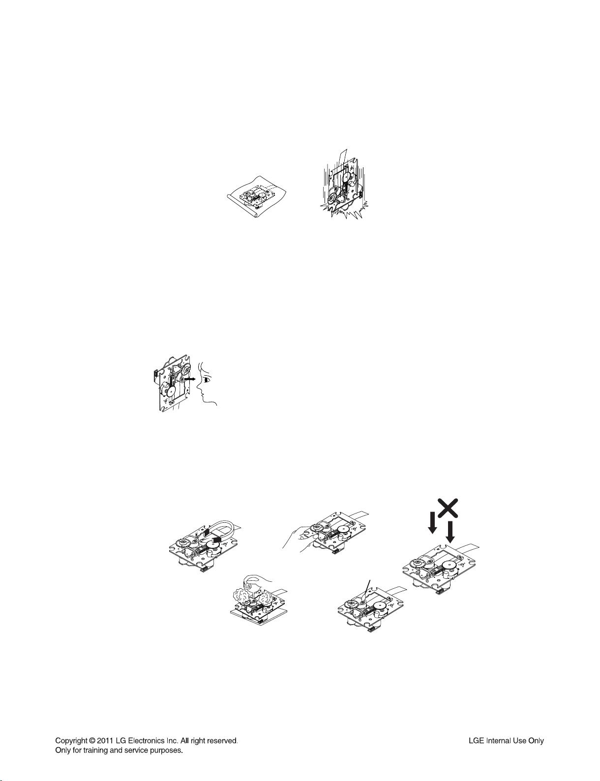
NOTES REGARDING HANDLING OF THE PICK-UP
1. Notes for transport and storage
1) The pick-up should always be left in its conductive bag until immediately prior to use.
2) The pick-up should never be subjected to external pressure or impact.
Storage in conductive bag
Drop impact
2. Repair notes
1) The pick-up incorporates a strong magnet, and so should never be brought close to magnetic materials.
2) The pick-up should always be handled correctly and carefully, taking care to avoid external pressure and
impact. If it is subjected to strong pressure or impact, the result may be an operational malfunction and/or
damage to the printed-circuit board.
3) Each and every pick-up is already individually adjusted to a high degree of precision, and for that reason
the adjustment point and installation screws should absolutely never be touched.
4) Laser beams may damage the eyes!
Absolutely never permit laser beams to enter the eyes!
Also NEVER switch ON the power to the laser output part (lens, etc.) of the pick-up if it is damaged.
NEVER look directly at the laser beam, and don’t allow
contact with fingers or other exposed skin.
5) Cleaning the lens surface
If there is dust on the lens surface, the dust should be cleaned away by using an air bush (such as used
for camera lens). The lens is held by a delicate spring. When cleaning the lens surface, therefore, a cotton
swab should be used, taking care not to distort lens.
Pressure
Magnet
How to hold the pick-up
Cotton swab
Conductive Sheet
6) Never attempt to disassemble the pick-up.
Spring has excess pressure. If the lens is extremely dirty, apply isopropyl alcohol to the cotton swab.
(Do not use any other liquid cleaners, because they will damage the lens.) Take care not to use too much
of this alcohol on the swab, and do not allow the alcohol to get inside the pick-up.
1-3
Pressure
Page 5
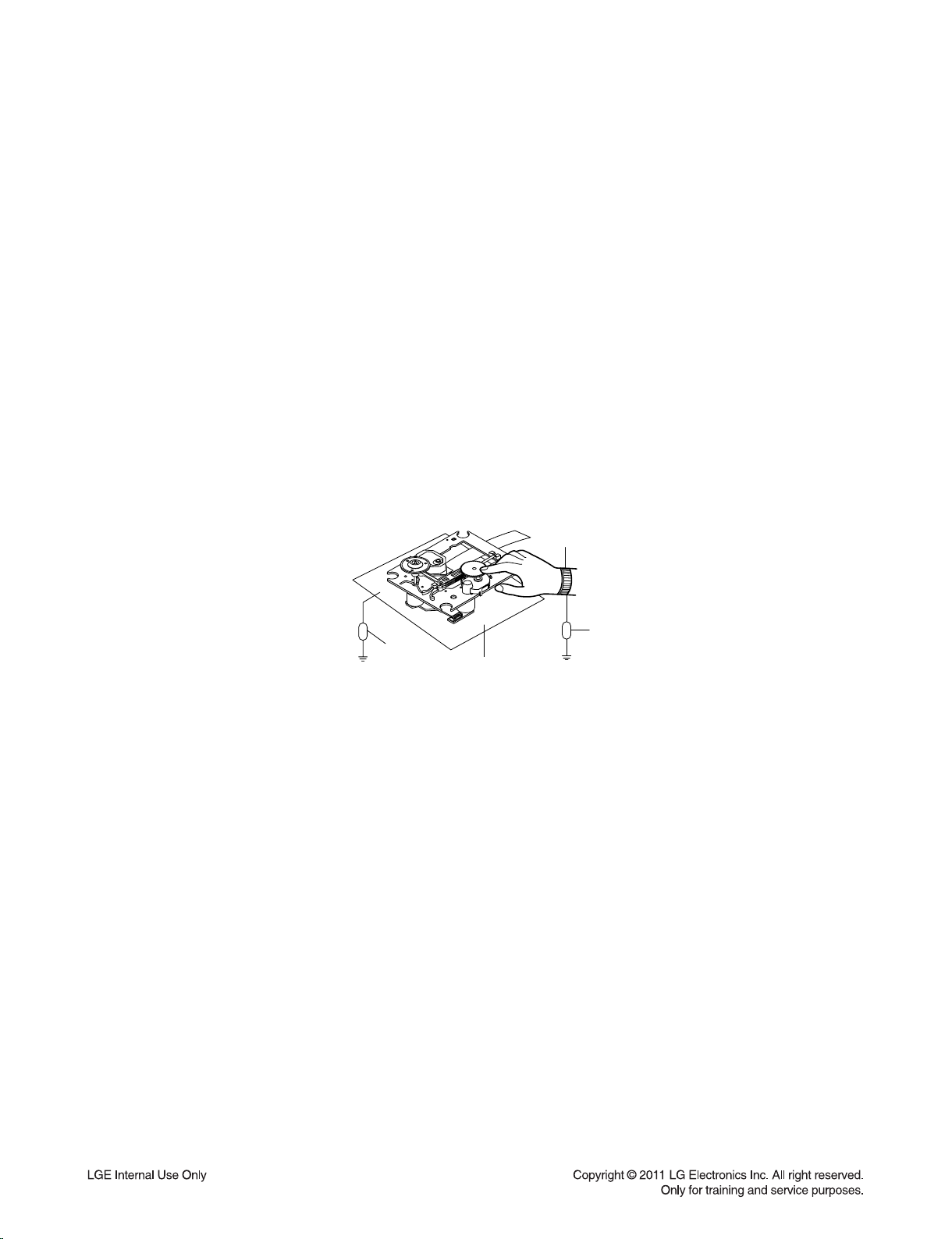
NOTES REGARDING COMPACT DISC PLAYER REPAIRS
1. Preparations
1) Compact disc players incorporate a great many ICs as well as the pick-up (laser diode). These components
are sensitive to, and easily affected by, static electricity. If such static electricity is high voltage, components
can be damaged, and for that reason components should be handled with care.
2) The pick-up is composed of many optical components and other high-precision components. Care must be
taken, therefore, to avoid repair or storage where the temperature or humidity is high, where strong magnetism is present, or where there is excessive dust.
2. Notes for repair
1) Before replacing a component part, first disconnect the power supply lead wire from the unit
2) All equipment, measuring instruments and tools must be grounded.
3) The workbench should be covered with a conductive sheet and grounded.
When removing the laser pick-up from its conductive bag, do not place the pick-up on the bag. (This is
because there is the possibility of damage by static electricity.)
4) To prevent AC leakage, the metal part of the soldering iron should be grounded.
5) Workers should be grounded by an armband (1 MΩ)
6) Care should be taken not to permit the laser pick-up to come in contact with clothing, in order to prevent static electricity changes in the clothing to escape from the armband.
7) The laser beam from the pick-up should NEVER be directly facing the eyes or bare skin.
Armband
Resistor
(1 MΩ)
Resistor
(1 MΩ)
Conductive
Sheet
1-4
Page 6
ESD PRECAUTIONS
Electrostatically Sensitive Devices (ESD)
Some semiconductor (solid state) devices can be damaged easily by static electricity. Such components
commonly are called Electrostatically Sensitive Devices (ESD). Examples of typical ESD devices are integrated
circuits and some field-effect transistors and semiconductor chip components. The following techniques should
be used to help reduce the incidence of component damage caused by static electricity.
1. Immediately before handling any semiconductor component or semiconductor-equipped assembly, drain off
any electrostatic charge on your body by touching a known earth ground. Alternatively, obtain and wear a
commercially available discharging wrist strap device, which should be removed for potential shock reasons
prior to applying power to the unit under test.
2. After removing an electrical assembly equipped with ESD devices, place the assembly on a conductive surface
such as aluminum foil, to prevent electrostatic charge buildup or exposure of the assembly.
3. Use only a grounded-tip soldering iron to solder or unsolder ESD devices.
4. Use only an anti-static solder removal device. Some solder removal devices not classified as "anti-static" can
generate electrical charges sufficient to damage ESD devices.
5. Do not use freon-propelled chemicals. These can generate electrical charges sufficient to damage ESD
devices.
6. Do not remove a replacement ESD device from its protective package until immediately before you are
ready to install it. (Most replacement ESD devices are packaged with leads electrically shorted together by
conductive foam, aluminum foil or comparable conductive materials).
7. Immediately before removing the protective material from the leads of a replacement ESD device, touch the
protective material to the chassis or circuit assembly into which the device will by installed.
CAUTION : BE SURE NO POWER IS APPLIED TO THE CHASSIS OR CIRCUIT, AND OBSERVE ALL OTHER
SAFETY PRECAUTIONS.
8. Minimize bodily motions when handing unpackaged replacement ESD devices. (Otherwise harmless motion
such as the brushing together of your clothes fabric or the lifting of your foot from a carpeted floor can generate
static electricity sufficient to damage an ESD device).
CAUTION. GRAPHIC SYMBOLS
THE LIGHTNING FLASH WITH APROWHEAD SYMBOL. WITHIN AN EQUILATERAL TRIANGLE, IS
INTENDED TO ALERT THE SERVICE PERSONNEL TO THE PRESENCE OF UNINSULATED
“DANGEROUS VOLTAGE” THAT MAY BE OF SUFFICIENT MAGNITUDE TO CONSTITUTE A RISK OF
ELECTRIC SHOCK.
THE EXCLAMATION POINT WITHIN AN EQUILATERAL TRIANGLE IS INTENDED TO ALERT THE
SERVICE PERSONNEL TO THE PRESENCE OF IMPORTANT SAFETY INFORMATION IN SERVICE
LITERATURE.
1-5
Page 7
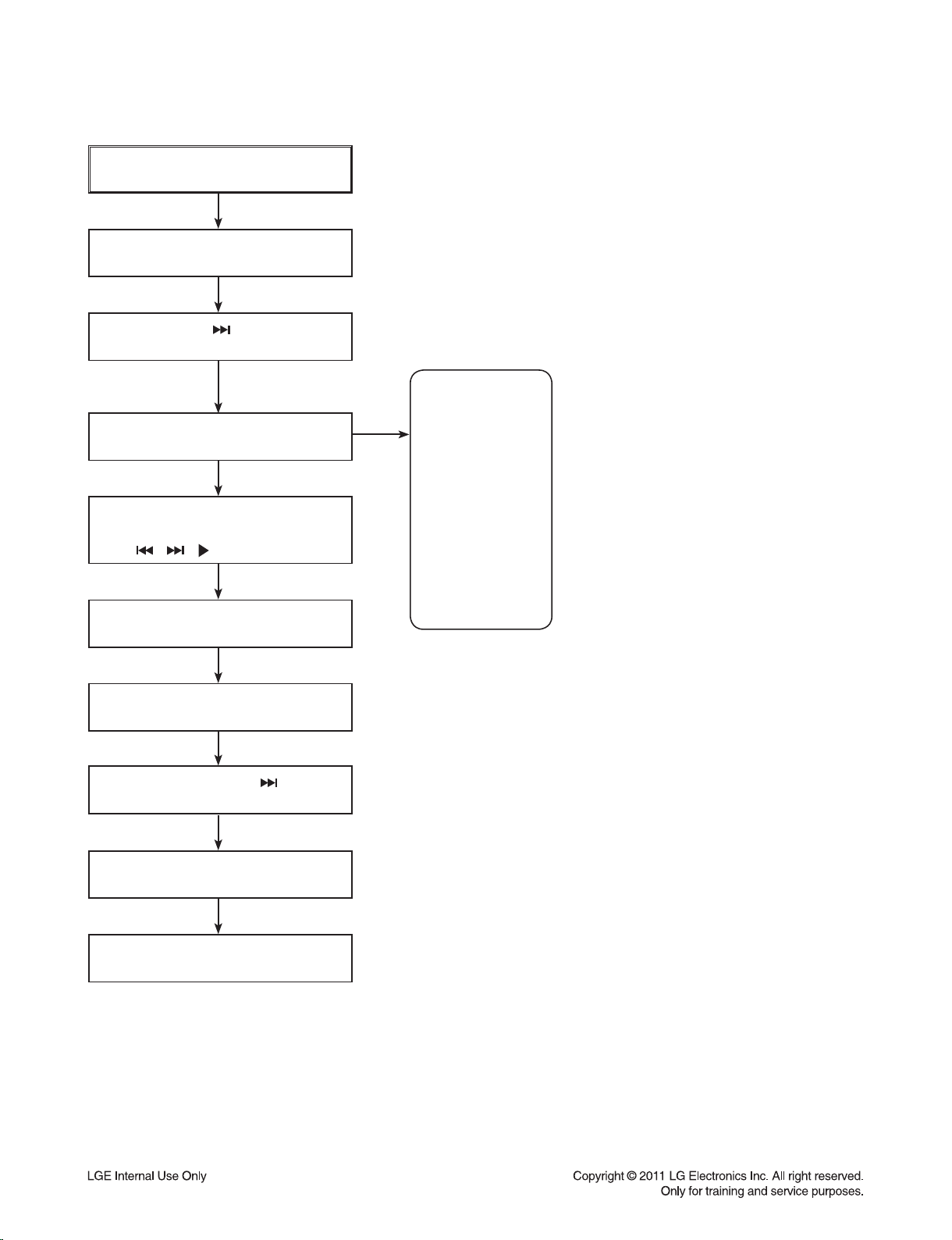
SERVICE INFORMATION FOR EEPROM
POWER ON
FLD no disc status
Remote control ‘
’ + Front ‘STOP’
push same timing during 5s
FLD ‘OP-0….
Move to appropriate position and
make changes with remote control.
( , , /■ , REPEAT )
Press STOP key
FLD ‘write ok’
DETECT NEW EEPROM
(OPTION EDIT SCREEN)
NAME
OP0
OP1
OP2
OP3
OP4
OP5
OP6
OP7
OP8
OP9
HEX
09
00
00
00
00
69
90
05
60
08
Remote control ‘
’ +
Front ‘STOP’ push same timing
FLD ‘E2P CLR’
Completed
1-6
Page 8
PROGRAM DOWNLOAD GUIDE
1. AUDIO PROGRAM
Download program file name must be RCD406_YYMMDDX.HEX
If security program (Water Wall) is activated on your PC, you must save the file to the usb storage
device and disable the security software, then download the file to your set.
Caution: When downloading the file, you should neither unplug the usb device, change to the other
function, nor power off the device. Usb device must be unplugged when the downloading
process is completed.
ON VFD DISPLAY SCREEN
NO USB
↓← Insert usb device at usb function
READ
↓
FIRMWARE
↓
WRITE 00 .. 100
↓
UPDATED
↓
POWER OFF AUTOMATICALLY
←
When completed, remove usb device.
1-7
Page 9
2. CD PROGRAM
Download program file name must be HD003_DATE_00.BIN
If security program (Water Wall) is activated on your PC, you must save the file to the usb storage
device and disable the security software, then download the file to your set.
Caution: When downloading the file, you should neither unplug the usb device, change to the other
function, nor power off the device. Usb device must be unplugged when the downloading
process is completed.
ON VFD DISPLAY SCREEN
NO USB
↓← Insert usb device at usb function
READ
↓
FIRMWARE
↓
FINISH
↓
UPDATED
↓
POWER OFF AUTOMATICALLY
←
When completed, remove usb device
.
1-8
Page 10

3. BEAT BOX PROGRAM
Download program file name must be BEAT_BIN_DATE_00.BIN
If security program (Water Wall) is activated on your PC, you must save the file to the usb storage
device and disable the security software, then download the file to your set.
Caution: When downloading the file, you should neither unplug the usb device, change to the other
function, nor power off the device. Usb device must be unplugged when the downloading
process is completed.
ON VFD DISPLAY SCREEN
NO USB
↓← Insert usb device at usb function
READ
↓
FIRMWARE
↓
FINISH
↓
UPDATED
↓
POWER OFF AUTOMATICALLY
←
When completed, remove usb device
.
1-9
Page 11

SPECIFICATIONS
• GENERAL
Power requirements Refer to main label
Power consumption Refer to main label
Dimensions (W x H x D) 285 x 350 x 380 mm without foot
Net Weight (Approx.) 6.6 kg
Operating temperature 5 °C to 35 °C (41 °F to 95 °F)
Operating humidity 5 % to 90 %
Bus Power Supply USB DC 5 V 500 mA
iPod DC 5 V 1 A
• INPUTS/ OUTPUTS
ANALOG AUDIO IN 1.2 Vrms (1 kHz, 0 dB), 600 Ω, RCA jack (L, R) x 1
PORT. IN 0.5 Vrms (3.5 mm stereo jack)
ANALOG AUDIO OUT 800 mVrms (1 kHz, 0 dB), 600 Ω, RCA jack (L, R) x 1
• TUNER
FM Tuning Range 87.5 to 108.0 MHz or 87.50 to 108.00 MHz
AM Tuning Range 522 to 1 620 kHz, 520 to 1 710 kHz or 522 to 1 710 kHz
• AMPLIFIER
Stereo mode 200 W + 200 W (4 Ω at 1 kHz)
• CD
Frequency Response 40 to 20 000 Hz
Signal-to-noise ratio 75 dB
Dynamic range 80 dB
• SPEAKERS
Front speaker
Type 2 Way 2 speaker
Impedance 4 Ω
Rated Input Power 200 W
Max. Input power 400 W
Net Dimensions (W x H x D) 239 x 400 x 335 mm
Net Weight 5 kg
• Design and specifications are subject to change without notice.
1-10
Page 12

SECTION 2
CABINET & MAIN CHASSIS
CONTENTS
DISASSEMBLY AND ASSEMBLY FOR MECHANISM DECK (CDM-H1803) ........................ 2-2
1. ORDER OF DISASSEMBLY FOR MECHANISM DECK .......................................................................... 2-2
2. ORDER OF ASSEMBLY FOR MECHANISM DECK ................................................................................ 2-6
EXPLODED VIEWS ................................................................................................................................... 2-11
1. CABINET AND MAIN FRAME SECTION (RCD406) .............................................................................. 2-11
2. MECHANISM DECK SECTION (CDM-H1803) ....................................................................................... 2-13
3. PACKING ACCESSORY SECTION ....................................................................................................... 2-15
4. SPEAKER SECTION .............................................................................................................................. 2-16
2-1
Page 13
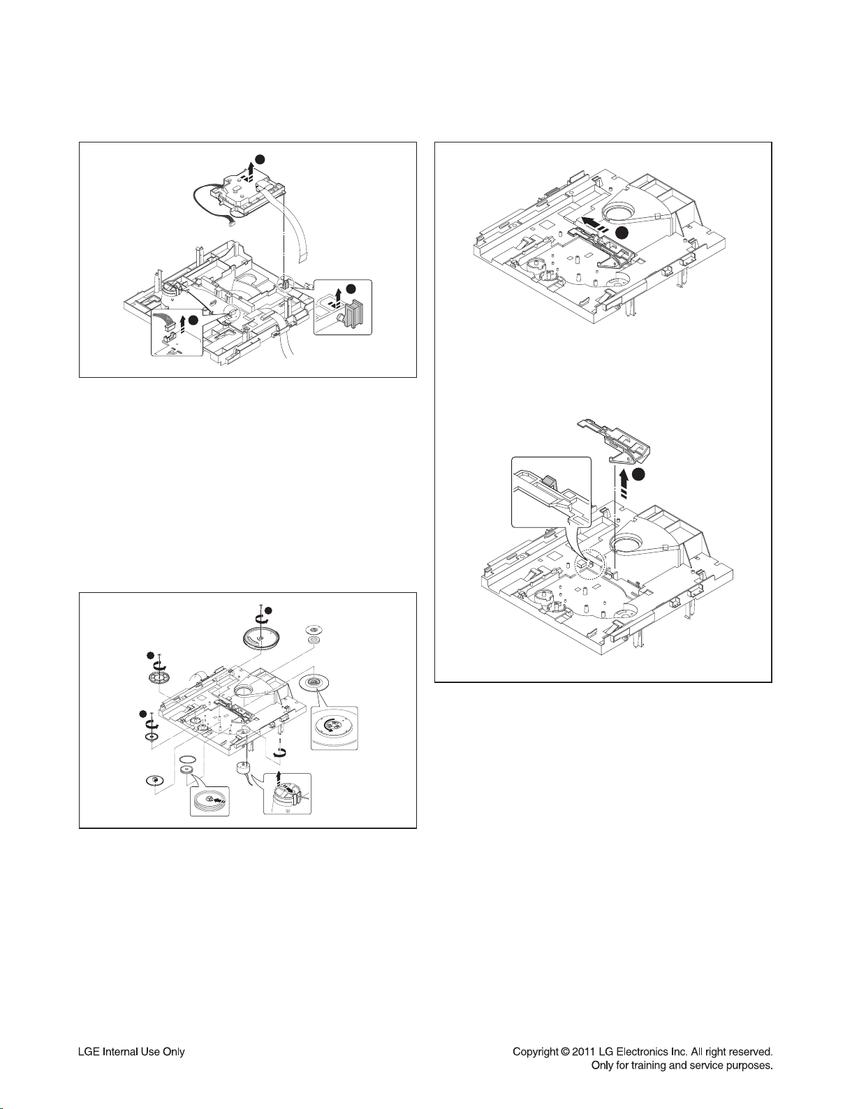
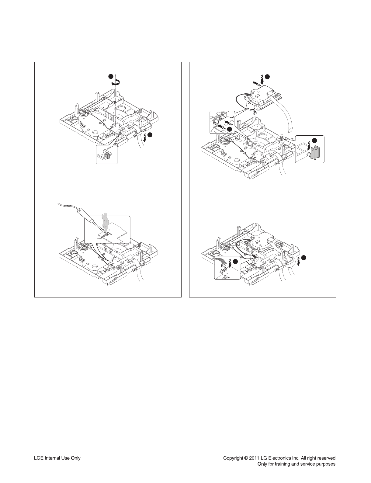
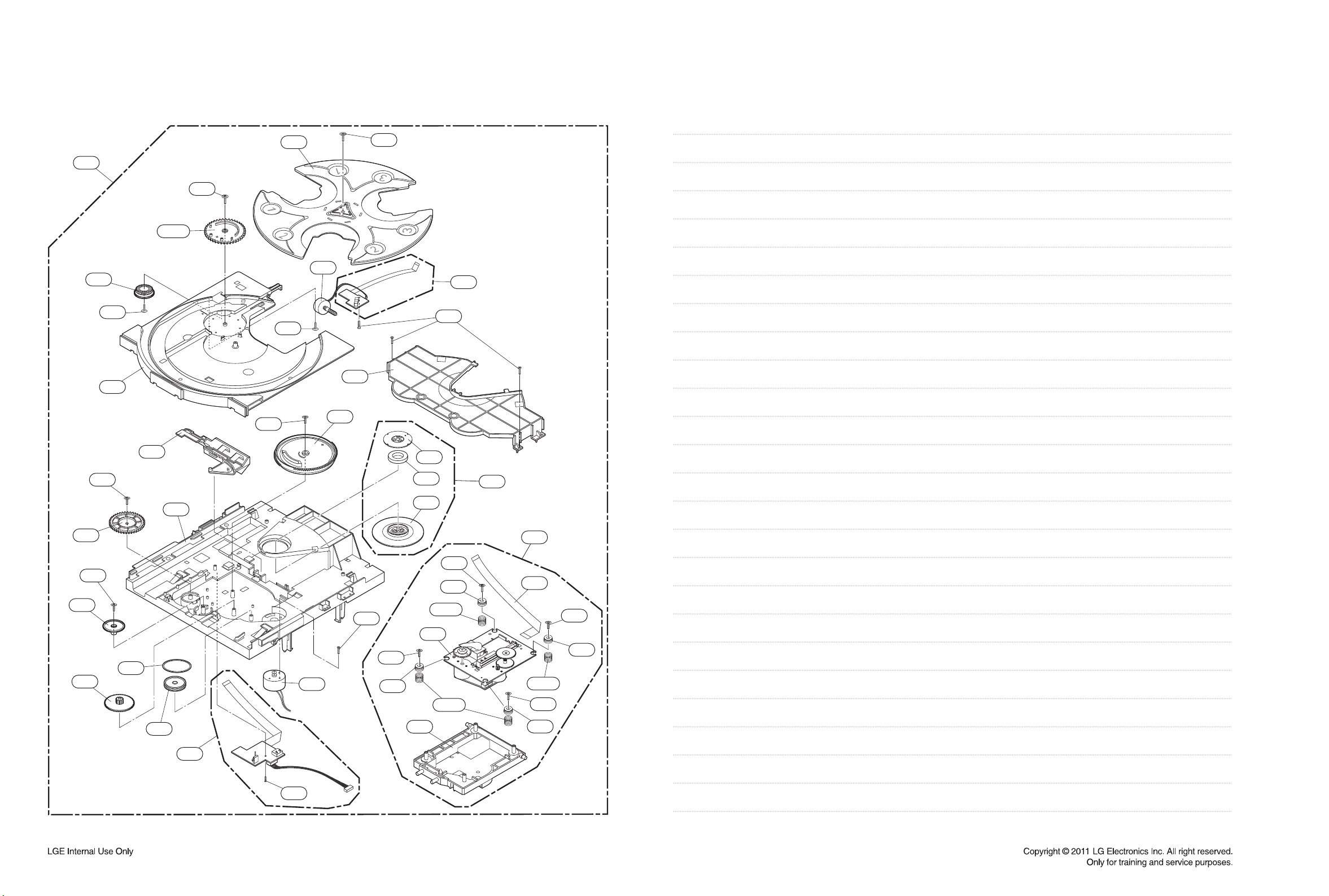
DISASSEMBLY AND ASSEMBLY FOR MECHANISM DECK (CDM-H1803)
1. ORDER OF DISASSEMBLY FOR MECHANISM DECK
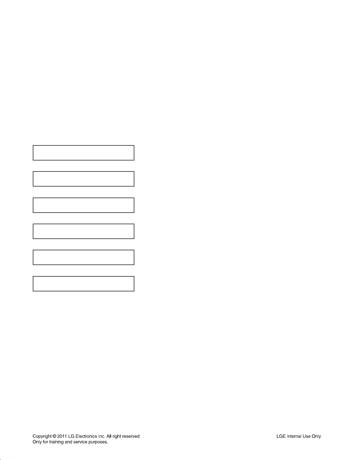
1) Disassemble the Cover Guide Disc.
Figure 1
2) Disassemble the Loading FFC from the Main PCB
Assy.
Turn the Gear in OPEN direction as shown in Figure 2
to take out the Tray Loading Assy in 3 direction.
2
1
3
Figure 2
3) Pull up the Holder 1 to completely disassemble the
1
2
Tray Loading Assy from the Base Main Assy.
Figure 3
2-2
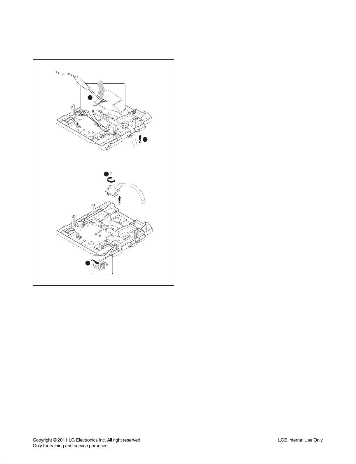
Page 14
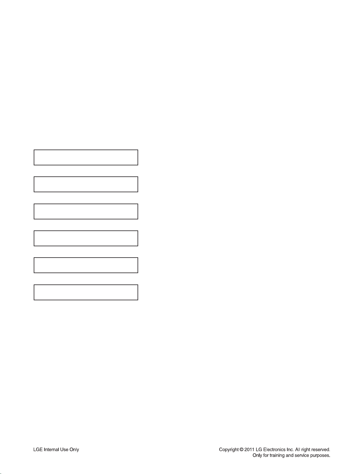
ORDER OF DISASSEMBLY FOR MECHANISM DECK
4) Loosen the screw to pull up and disassemble the
1
2
Figure 4
Tray Disc.
5) Loosen the screw to pull up and disassemble the
Gear Tray CAM.
Figure 5
Figure 6
6) Disassemble the Gear Tray, Tray Motor Assy and
Loading PCB Assy from the Tray Loading.
2-3
Page 15
ORDER OF DISASSEMBLY FOR MECHANISM DECK
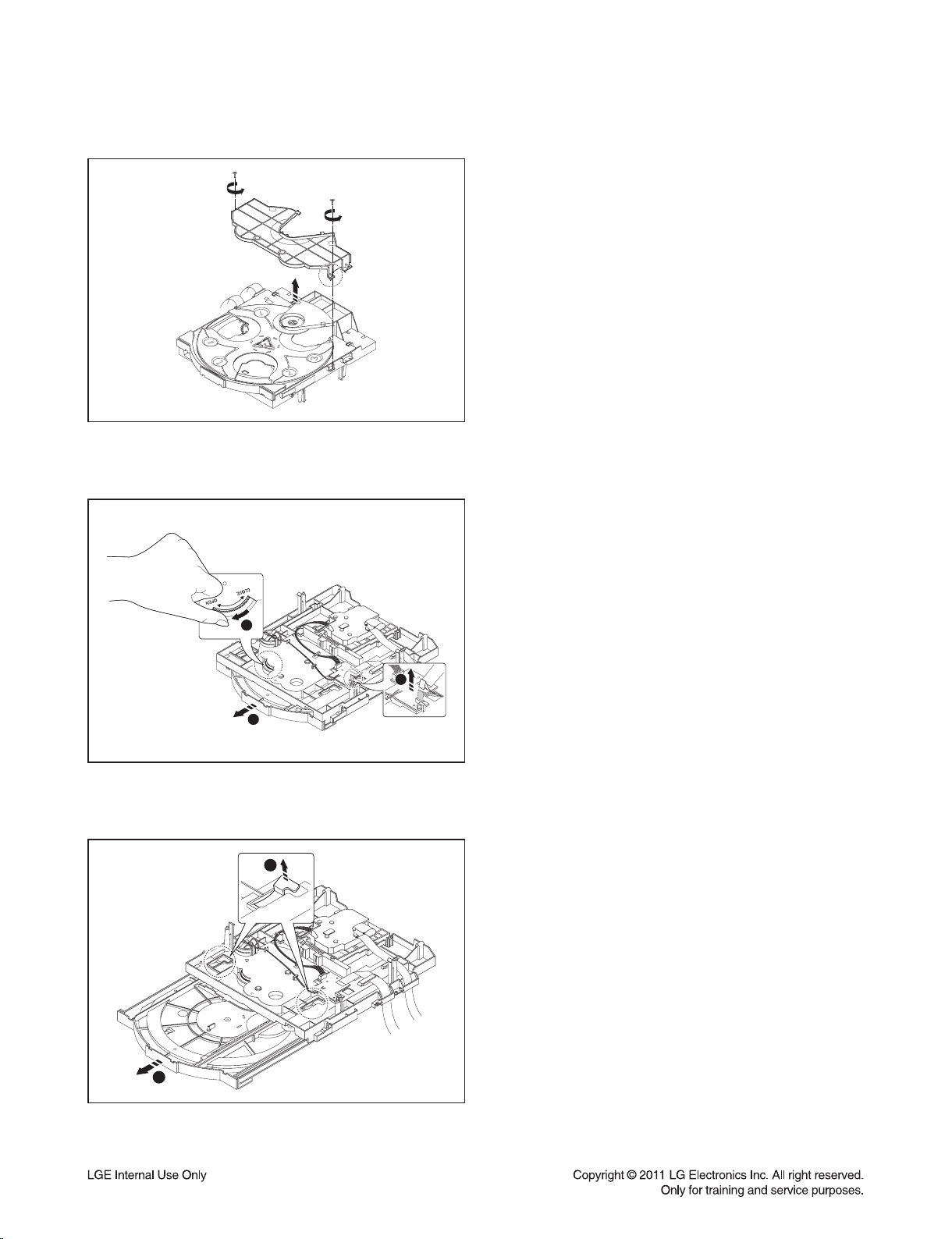
3
2
1
Figure 7
7) Disassemble the Harness Cable from the Base
Main.
Disassemble the Base Sled Assy from the Base Main
by referring to Figure.
1
2
3
1
2
Figure 8
8) Disassemble each gear part, Clamp Disc, Clamp
Magnet and Cover Plate from the Base Main.
Disassemble the Loading Motor Assy by being careful
of the hook on the surface of the Base Main.
Figure 9
9) Push the Guide UD in direction 1 to disassemble it
from the Base Main.
2-4
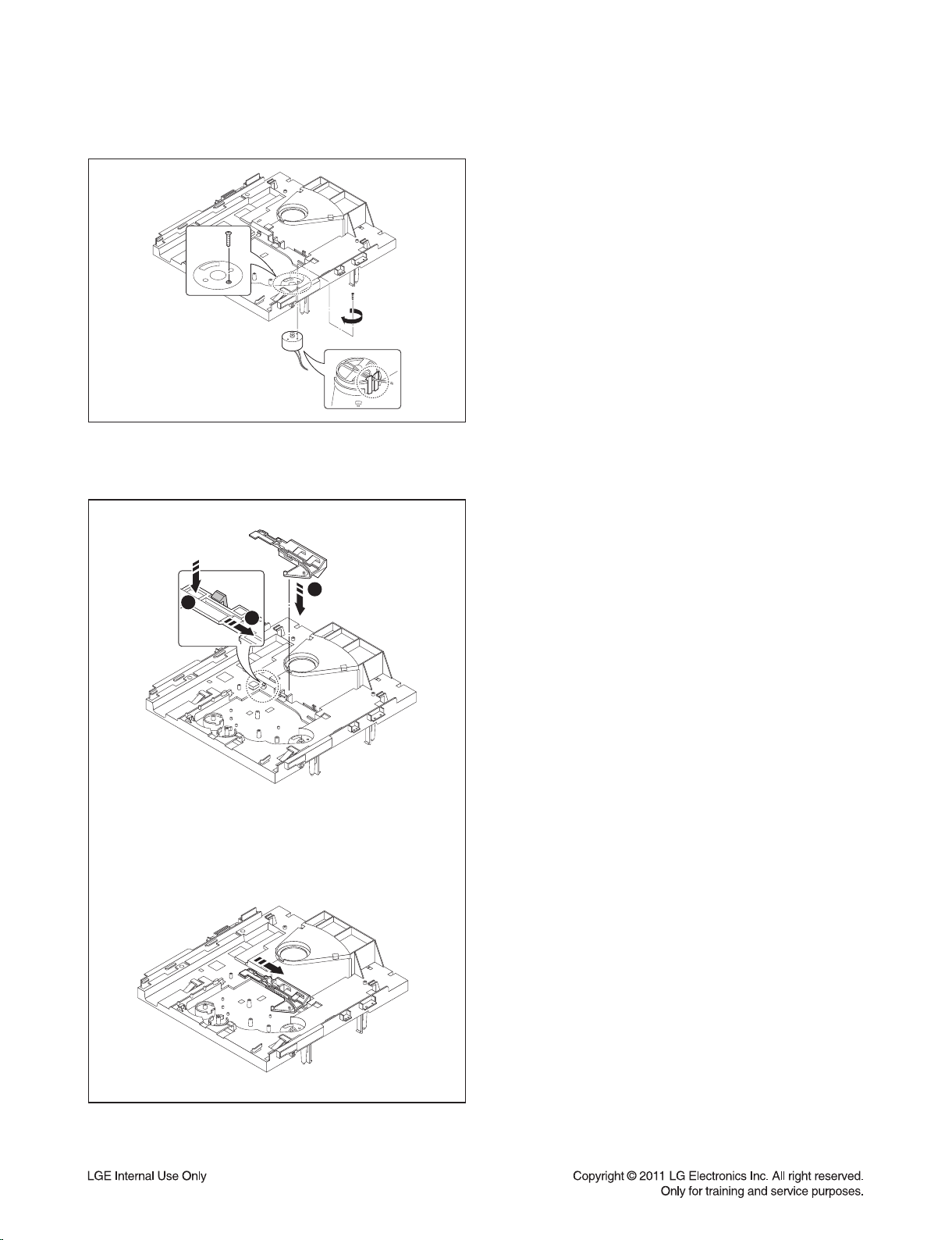
Page 16
ORDER OF DISASSEMBLY FOR MECHANISM DECK
10) Use a solder to remove the Motor Jump Wire from
the Main PCB Assy and then disassemble the FFC
Cable.
Loosen the screw to disassemble the Main PCB Assy.
1
2
4
3
Figure 10
2-5
Page 17
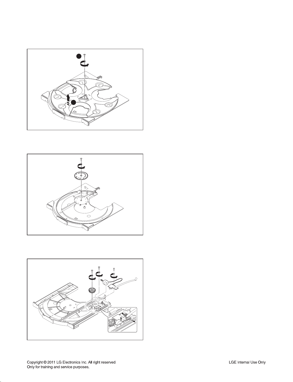
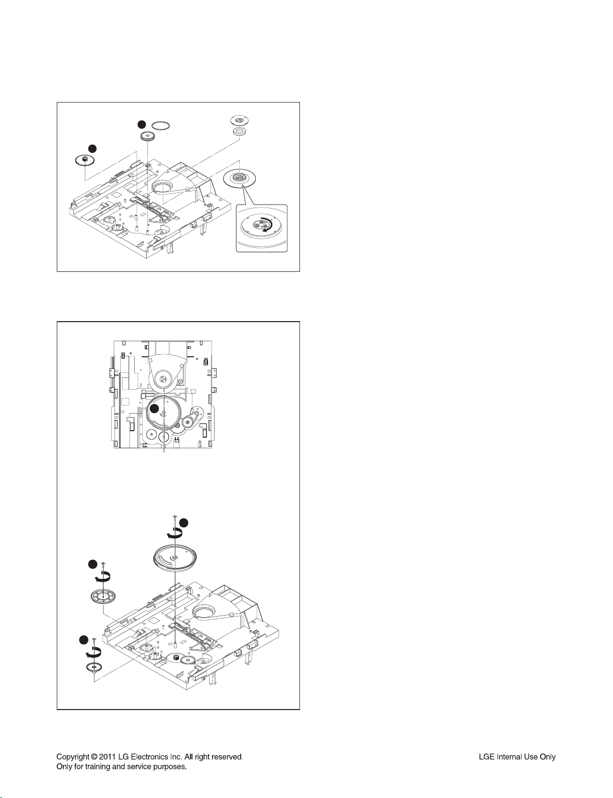
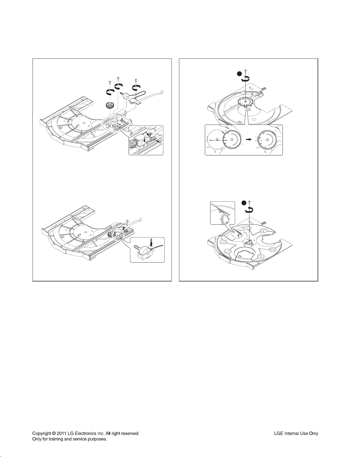
2. ORDER OF ASSEMBLY FOR MECHANISM DECK
1) Assemble the Loading Motor Assy to the Base
Main.
(When assembling the Motor Assy, use the hook on
the surface of the Base Main to preassemble, and then
tighten the screws.)
Figure 1
2) Set the Guide UD on the Base Main.
After setting the part, push it in direction 3.
2
3
1
Figure 2
2-6
Page 18
ORDER OF ASSEMBLY FOR MECHANISM DECK
3) Set the Gear Loading 1 and Gear Pulley 2 on the
2
1
Figure 3
Base Main.
Hang the belt between the Gear Pulley and Motor Pulley.
Assemble the Clamp Disc, Clamp Magnet and Cover
Plate to the Base Main.
4) After setting the Gear Main 2, Gear Pu Up 3 and Gear
Pu Down 4 on the Base Main, tighten the screws.
After assembling the Gear Main, align the location as
shown in Figure.
1
2
4
3
Figure 4
2-7
Page 19
ORDER OF ASSEMBLY FOR MECHANISM DECK
1
1
2
2
3
Figure 5
5) After setting the Main PCB Assy on the Base Main,
tighten the screw.
(Set the part accurately on the hook)
Solder the Motor Jump Wire on the PCB set on the
Base Main.
5
4
Figure 6
6) Set the Base Sled Assy on the Base Main.
(When setting the part, assemble with the CAM part of
the Guide UD inserted in two locations of the Boss of
Frame UD)
Align the FFC to the Guide and connect the Harness
Cable.
2-8
Page 20
ORDER OF ASSEMBLY FOR MECHANISM DECK
1
2
Figure 7
7) After setting the Gear Tray, Tray Motor Assy and
Loading PCB Assy on the Tray Loading, tighten the
screw.
Figure 8
8) Assemble the Gear Tray CAM on the Tray Loading
and set the Tray Disc.
(When assembling, check the location of the Gear Tray
CAM and Tray Disc as shown in the Figure)
2-9
Page 21
ORDER OF ASSEMBLY FOR MECHANISM DECK
1
2
3
Figure 9 Figure 10
9) Assemble the Tray Loading Assy on the Base Main
Assy as shown in the Figure.
After assembling, insert the Loading FFC to the 5 Pin
Wafer of Main PCB Assy.
10) After setting the Cover Guide Disc, tighten the
screw.
2-10
Page 22
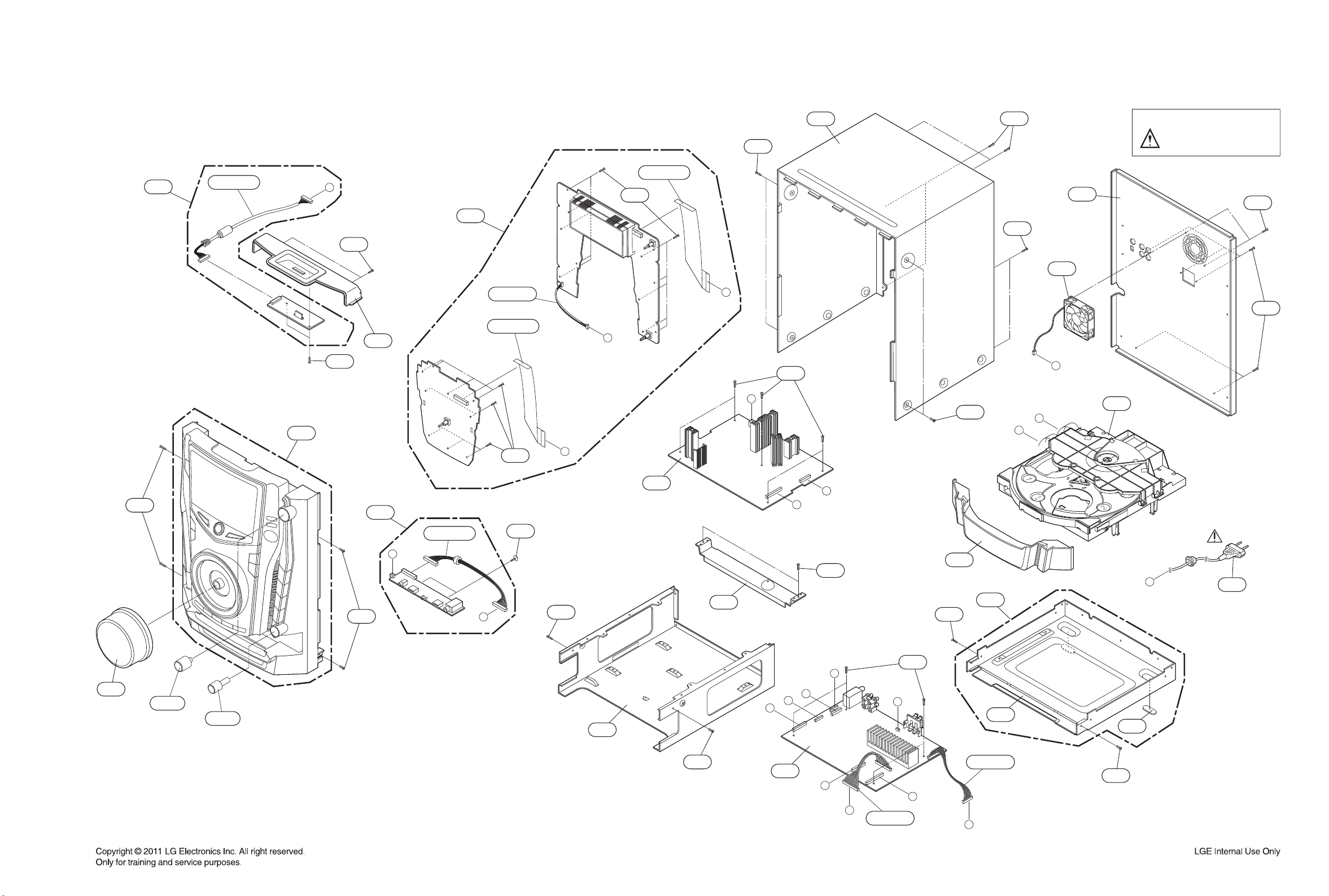
EXPLODED VIEWS
1. CABINET AND MAIN FRAME SECTION (RCD406)
464
A49
CABLE1
A42
E
iPod
464
464
264
A45
A43
VOLUME
CABLE2
CN302
CABLE7
464
480
NOTES) THE EXCLAMATION POINT WITHIN AN
EQUILATERAL TRIANGLE IS INTENDED
TO ALERT THE SERVICE PERSONNEL
TO THE PRESENCE OF IMPORTANT
SAFETY INFORMATION IN SERVICE
LITERATURE.
464
268
464
CABLE6
270
464
VFD
464
464
269
I
464
K
463
C
464
F
H
J
A26
D
SMPS
A47
A
B
251
255A
255C
464
K
USB+MIC
463
267
C
G
464
464
265
A44
300
463
D
E
266
F
G
J
271
272
MAIN
464
A46
H
B
CN102
I
CN101
464
A
2-11 2-12
Page 23
2. MECHANISM DECK SECTION (CDM-H1803)
MEMO
A26
153
443
159
173
153A
443
416
151
443
416
155
156
422
182
177
001
166
167
164
417
417
162
163
172
165
422
175
440
421
012
002
003
180
012B
137
421
012
012A
A02
A01
010
421
012
012B
421
012
2-13 2-14
Page 24
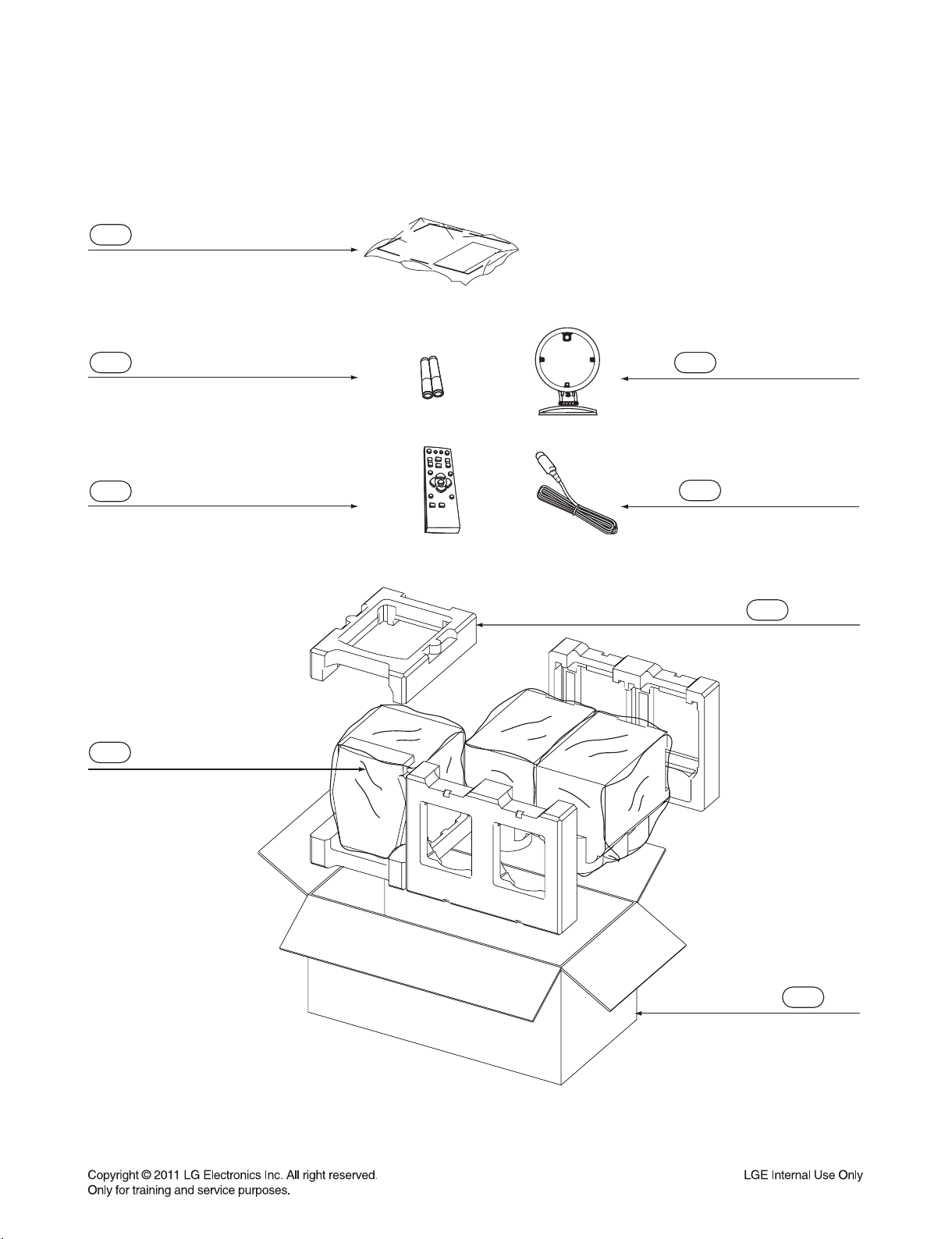
3. PACKING ACCESSORY SECTION
801 Owner’s Manual
AAA
808 Battery
AAA
824 AM Loop Antenna
900 Remote Control
804 Bag
825 FM Wire Antenna
803 Packing
2-15
802 Box
Page 25
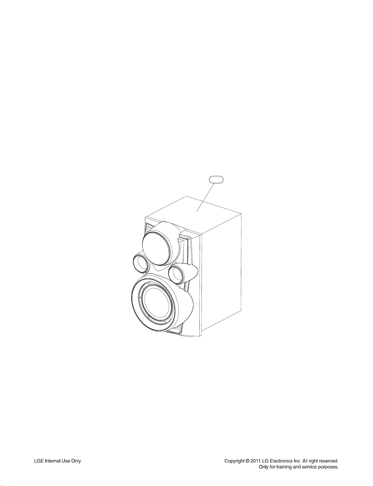
4. SPEAKER SECTION
4-1. FRONT SPEAKER (RCS606F)
A60
2-16
Page 26

SECTION 3 ELECTRICAL
CONTENTS
TRAINING MASTER ................................................................................................................................... 3-2
1. NO SOUND FROM SPEAKERS ............................................................................................................ 3-2
2. NO SOUND IN AUX FUNCTION ............................................................................................................ 3-3
3. NO SOUND IN PORT. IN FUNCTION ................................................................................................... 3-4
4. NO SOUND IN IPOD FUNCTION .......................................................................................................... 3-5
5. NO SOUND IN AM/FM FUNCTION ....................................................................................................... 3-6
6. NO SOUND IN CD FUNCTION .............................................................................................................. 3-7
7. NO SOUND IN USB FUNCTION ............................................................................................................ 3-9
8. NO POWER .......................................................................................................................................... 3-10
ONE POINT REPAIR GUIDE ................................................................................................................. 3-11
1. NO POWER .......................................................................................................................................... 3-11
2. NO BOOTING WHEN POWER ON THE SET ..................................................................................... 3-13
3. VFD IS NOT DISPLAYED WHEN POWER ON THE SET ................................................................... 3-14
4. NO OPERATION OF MD ..................................................................................................................... 3-15
5. NO SOUND .......................................................................................................................................... 3-21
ELECTRICAL TROUBLESHOOTING GUIDE .................................................................................. 3-29
1. POWER SUPPLY ON SMPS BOARD ................................................................................................. 3-29
2. SYSTEM PART .................................................................................................................................... 3-33
3. NO AUDIO PART ................................................................................................................................. 3-34
4. DIGITAL AUDIO AMP CHECK ............................................................................................................. 3-39
WAVEFORMS ............................................................................................................................................. 3-40
WIRING DIAGRAM ................................................................................................................................... 3-43
BLOCK DIAGRAMS ................................................................................................................................. 3-45
1. OVERALL BLOCK DIAGRAM .............................................................................................................. 3-45
2. SMPS BLOCK DIAGRAM..................................................................................................................... 3-47
3. POWER BLOCK DIAGRAM ................................................................................................................. 3-49
CIRCUIT DIAGRAMS ............................................................................................................................... 3-51
1. SMPS CIRCUIT DIAGRAM .................................................................................................................. 3-51
2. MICOM CIRCUIT DIAGRAM ................................................................................................................ 3-53
3. PWM CIRCUIT DIAGRAM .................................................................................................................... 3-55
4. AMP CIRCUIT DIAGRAM ..................................................................................................................... 3-57
5. DSP CIRCUIT DIAGRAM ..................................................................................................................... 3-59
6. RF SERVO CIRCUIT DIAGRAM .......................................................................................................... 3-61
7. ADC CIRCUIT DIAGRAM ..................................................................................................................... 3-63
8. BEAT BOX CIRCUIT DIAGRAM .......................................................................................................... 3-65
9. VFD CIRCUIT DIAGRAM ..................................................................................................................... 3-67
10. VOLUME CIRCUIT DIAGRAM ............................................................................................................. 3-69
11. USB & MIC CIRCUIT DIAGRAM .......................................................................................................... 3-71
12. IPOD CIRCUIT DIAGRAM .................................................................................................................... 3-73
CIRCUIT VOLTAGE CHART ................................................................................................................. 3-75
PRINTED CIRCUIT BOARD DIAGRAMS ......................................................................................... 3-79
1. MAIN P.C.BOARD ................................................................................................................................ 3-79
2. SMPS P.C.BOARD ............................................................................................................................... 3-83
3. VFD P.C.BOARD .................................................................................................................................. 3-85
4. VOLUME P.C.BOARD .......................................................................................................................... 3-87
5. USB & MIC P.C.BOARD ...................................................................................................................... 3-89
6. IPOD P.C.BOARD ................................................................................................................................ 3-89
3-1
Page 27
TRAINING MASTER
1. NO SOUND FROM SPEAKERS
Are the speaker cables connected correctly
between the speaker terminals on the unit
and the speakers?
YES
Does the customer select correctly
the input function he or she wants to listen to?
YES
After pressing FUNCTION,
is “CD, USB, AUX, IPOD, AM or FM” displayed?
YES
Turn the master volume clockwise
for the volume up.
YES
NO
NO
NO
NO
Make sure to connect the cables to each specified
connector tightly on the unit.
Connect the woofer cables to the WOOF SYSTEM
connectors on the rear panel.
Make sure to connect some cables like A/V cables
and FM/AM antenna cables.
Make sure to select the desired input function
pressing FUCTION button.
The volume level LEDs around the master volume
will be turned on more and more
while turning it clockwise for the volume up.
Is there any sound from the selected input source?
(AUX IN, USB, TUNER or CD Disc)
YES
Are the sound spectrum level LEDs
on the left and right side of the front panel
being changed up and down
according to the sound input gain?
YES
The sound is output from the speakers.
YES
Sound OK
NO
NO
Refer to a device’s instruction manual
and then check if there is sound output from it
connecting another audio system.
The sound spectrum level LEDs will be turned on/off
repeatedly at regular intervals. The speakers cables
might be short-circuited with the chassis ground.
Be careful not to be shorted each other.
3-2
Page 28
TRAINING MASTER
2. NO SOUND IN AUX FUNCTION
Does the customer select correctly
the AUX function he or her wants to listen to?
YES
After pressing the FUNCTION,
is “AUX” displayed on VFD?
YES
Turn the master volume clockwise
for the volume up.
YES
Is there any sound
from the selected input source?
YES
NO
NO
NO
NO
Make sure to connect some cables
between the AUX IN jacks of the unit
and the Audio output jacks of a external Audio device.
Make sure to select the AUX IN function
pressing the AUX/IPOD/PORT. IN button.
The volume level LEDs around the master volume
will be turned on more and more
while turning it clockwise for the volume up.
Refer to a device’s instruction manual
and then check if there is sound output
from it connecting another audio system
Are the sound spectrum level LED’s
on the left and right side of the front panel
being changed up and down
according to the sound input gain?
YES
Are the speaker cables connected correctly
between the speaker terminals on the unit
and the speakers?
YES
The sound is output
from the speakers.
YES
Sound OK
NO
NO
The sound spectrum level LED’s will be turned on/off
repeatedly at regular intervals. A speaker cable
might be short-circuited with the chassis ground.
Be careful not to be shorted each other.
Make sure to connect the cables to each specified
connector tightly on the unit.
Connect the woofer cables to the WOOF SYSTEM
connectors on the rear panel.
3-3
Page 29

TRAINING MASTER
3. NO SOUND IN PORT. IN FUNCTION
Does the customer select correctly
the PORT. IN function he or her wants to listen to?
YES
Is “PORT. IN” displayed on VFD?
YES
Turn the master volume clockwise
for the volume up.
YES
Is there any sound
from the selected input source?
YES
NO
NO
NO
NO
Make sure to connect a cable
between the PORT. IN jack of the unit and the Audio
output jack of a portable device like a MP3 player.
Make sure to select the PORT. IN function
pressing the AUX/IPOD/PORT. IN button.
The volume level LEDs around the master volume
will be turned on more and more
while turning it clockwise for the volume up.
Refer to a portable device’s instruction manual
and then check if there is sound output
from it connecting another audio system.
Are the sound spectrum level LED’s
on the left and right side of the front panel
being changed up and down
according to the sound input gain?
YES
Are the speaker cables connected correctly
between the speaker terminals on the unit
and the speakers?
YES
The sound is output
from the speakers.
YES
Sound OK
NO
NO
The sound spectrum level LED’s will be turned on/off
repeatedly at regular intervals. A speaker cable
might be short-circuited with the chassis ground.
Be careful not to be shorted each other.
Make sure to connect the cables to each specified
connector tightly on the unit.
Connect the woofer cables to the WOOF SYSTEM
connectors on the rear panel.
3-4
Page 30

TRAINING MASTER
4. NO SOUND IN IPOD FUNCTION
Does the customer select correctly
the iPod function he or she wants to listen to?
YES
Does the customer use the compatible iPod?
YES
After displaying “Loading”,
is “IPOD” displayed on VFD?
YES
After selecting desired songs
using the user interface of a iPod or a iPhone,
press PALY button and turn the master volume
clockwise for the volume up.
YES
NO
NO
NO
NO
Make sure to put a iPod or a iPhone
on the docking system on the top of the unit.
Make sure that The unit supports the models
as follows/iPod nano 1 G, 2 G, 3 G, 4 G, 5 G, 6 G/
iPod classic/ iPod 4 G, 5 G/
iPod touch 2 G, 3 G, 4 G/ iPhone 3 G, 4 G/.
If “ERROR”message is displayed, make sure firmly to put a
iPod or a iPhone on the docking system on the top of the unit.
When the battery of a iPod or a iPhone is fully discharged, the
unit can not detect IPOD function, Please wait for a moment
and then it will work after charging a little.
The volume level LEDs around the master volume
will be turned on more and more
while turning it clockwise for the volume up.
Refer to a device’s instruction manual
and then check if there is sound output
from it connecting another audio system.
Is there any sound from iPod or iPhone?
NO
YES
Are the sound spectrum level LED’s
on the left and right side of the front panel
being changed up and down
according to the sound input gain?
NO
The sound spectrum level LED’s will be turned on/off
repeatedly at regular intervals. A speaker cable might
be short-circuited with the chassis ground.
Be careful not to be shorted each other.
YES
Are the speaker cables connected correctly
between the speaker terminals on the unit
and the speakers?
NO
Connect the woofer cables to the WOOF SYSTEM
Maker sure to connect the cables
to each specified connector tightly on the unit.
connectors on the rear panel.
YES
The sound is output from the speakers. Sound OK
YES
3-5
Page 31

TRAINING MASTER
5. NO SOUND IN AM/FM FUNCTION
Does the customer select correctly
the AM/FM function he or she wants to listen to?
NO
Make sure to connect AM/FM antennas
on the rear panel of the unit.
YES
Is “AM or FM” displayed on VFD?
NO
Make sure to select AM or FM function
pressing the FUNC button.
YES
After tuning a desired channel
using the TUNING± button,
is the sound quality good to listen to the music?
NO
To prevent noise pickup, keep the AM Loop
antenna away from the unit and other components.
Be sure to fully extend the FM wire antenna. After
connecting the FM wire antenna, keep it horizontal.
YES
Is the signal strength of the radio station too week? Make sure to tune the station manually.
NO
YES
Are the sound spectrum level LED’s
on the left and right side of the front panel
being changed up and down
according to the sound input gain?
YES
Are the speaker cables connected correctly
between the speaker terminals on the unit
and the speakers?
YES
The sound is output
from the speakers.
YES
Sound OK
NO
NO
The sound spectrum level LED’s will be turned on/off
repeatedly at regular intervals. A speaker cable might
be short-circuited with the chassis ground.
Be careful not to be shorted each other.
Make sure to connect the cables to each specified
connector tightly on the unit.
Connect the woofer cables to the WOOF SYSTEM
connectors on the rear panel.
3-6
Page 32

TRAINING MASTER
6. NO SOUND IN CD FUNCTION
Does the customer select correctly
the CD function he or she wants to listen to?
NO
Make sure to put on a CD disc on the tray.
YES
Is a CD disc put on the tray correctly? Make sure to insert the CD disc upside down.
NO
YES
Does the unit display “NO DISC” on VFD
when a disc is inserted on the tray?
NO
Place the disc with the label
or printed side facing upwards.
YES
Does the customer use
the supported mp3 or WMA music files on the disc?
NO
Check the playable disc.
Make sure that the file extensions
are “.mp3” or “.wma”.
YES
When the unit searches music files in a CD disc,
are the following messages displayed on VFD?
“SELECTED” “TRACKING #” and “TIME”
YES
After selecting a track number using the SCAN or
DISC# button, press PLAY button and turn the master
volume clockwise for the volume up.
YES
Is the sound quality good to listen to the music?
YES
Are the sound spectrum level LED’s
on the left and right side of the front panel
changed up and down
according to the sound input gain?
YES
NO
NO
NO
NO
Make sure to check
the supported MP3/WMA music file on the CD disc.
Refer to the owner’s manual.
The volume level LEDs around the master volume
will be turned on more and more
while turning it clockwise for the volume up.
Make sure to clean CD discs with a commercially
available cleaner. If the surface of the disc is polluted
or scratched, the sound quality can become bad
or the customer can not listen to the music.
The sound spectrum level LED’s will be turned on/off
repeatedly at regular intervals. A speaker cable
might be short-circuited with the chassis ground.
Be careful not to be shorted each other.
3-7
Page 33

YES
TRAINING MASTER
Are the speaker cables connected correctly
between the speaker terminals on the unit
and the speakers?
YES
YES
The sound is output from the speakers. Sound OK
NO
NO
NO
NO
Connect the woofer cables to the WOOF SYSTEM
Maker sure to connect the cables
to each specified connector tightly on the unit.
connectors on the rear panel.
3-8
Page 34

TRAINING MASTER
7. NO SOUND IN USB FUNCTION
Does the customer select correctly
the USB function he or she wants to listen to?
YES
Is “USB” displayed on VFD?
YES
Does the unit display “SELECTED” on VFD
when a USB is inserted into the USB port?
YES
Does the customer use the supported
mp3 or WMA music files on the disc?
YES
NO
NO
NO
NO
Make sure to insert a USB on the USB ports
on the bottom of the unit.
Make sure to select the USB function
pressing the CD/USB button.
When “No USB” is displayed,
make sure that the customer uses the recommended
USB which support USB2.0 or USB1.1.
Check if it is the playable disc or not.
Make sure that the file extensions are
“.mp3”or “.wma”.
When the unit searches music files in a USB,
are the following messages displayed on VFD?
“SELECTED” “TRACKING #” and “TIME”
YES
After selecting a track number using the SCAN button,
press PLAY button and turn the master volume
clockwise for the volume up.
YES
Are the sound spectrum level
on the left and right side of the front panel
being changed up and down
according to the sound input gain?
YES
Are the speaker cables connected correctly
between the speaker terminals on the unit
and the speakers?
YES
NO
NO
NO
NO
Make sure to check the compatible USB device
and the supported MP3/WMA music file requirement.
Refer to the owner’s manual.
The volume level LEDs around the master volume
will be turned on more and more
while turning it clockwise for the volume up.
The sound spectrum level will be turned on/off
repeatedly at regular intervals. A speaker cable
might be short-circuited with the chassis ground.
Be careful not to be shorted each other.
Make sure to connect the cables
to each specified connector tightly on the unit.
Connect the woofer cables to the WOOF SYSTEM
connectors on the rear panel.
3-9
Page 35

YES
TRAINING MASTER
The sound is output from the speakers. Sound OK
8. NO POWER
Is the power cord plugged
into a electrical outlet?
Does the Standby LED light
YES
in red color?
YES
NO
NO
NO
Make sure to plug the power cord of the unit
into a electrical outlet.
If the customer can not see the red light
on the front panel, the SMPS might have any problem.
Please solve the problem
referring to the service manual.
Is the Standby LED turned off
after pressing the Power button
on the remote control?
YES
Are the messages displayed
in the following order on VFD?
“HELLOW” “VOLUME 15” “FUNCTION”
YES
Is there any sound
from the speakers each input function?
YES
Power & Sound OK
NO
NO
NO
Replace the batteries with new ones
if the remote control doesn’t work.
The SMPS might be not able to supply the power
to drive the VFD.
Refer to the service manual to fix it.
Make sure to connect speaker cables.
3-10
Page 36

ONE POINT REPAIR GUIDE
1. NO POWER
If the unit doesn’t work by no power problem, repair the set according to the following
guide.
1-1. FUSE & BRIDGE DIODE
1-1-1. Solution
Please check and replace F901, BD901, TH901, TH903 on SMPS board.
1-1-2. How to troubleshoot (Countermeasure)
1) Check if the fuse F901 is open or short-circuit.
2) Check if the bridge diode DB901 is short-circuit by over current with a digital multi meter.
3) Check if the NTC thermistor TH901 and TH902 is normal or open.
1-1-3. Service hint (Any picture / Remark)
< F901 >
If F901 is not short-circuit,
replace it with a same
specifi cations one.
replace it with a new one.
< BD901 >
If BD901 is short-circuit,
< TH901, TH903 >
If TH901 or TH902 is open,
replace it with a new one.
3-11
Page 37

ONE POINT REPAIR GUIDE
NO POWER
If the unit doesn’t work by no power problem, repair the set according to the following
guide.
1-2. D951, ZD951
1-2-1. Solution
Please check and replace D951, ZD951 on SMPS board.
1-2-2. How to troubleshoot (Countermeasure)
1) Check the Anode-Cathod Voltage of D951 with a digital multi-meter, it is normally 0.2 ~ 0.3 V.
If it doesn’t have any voltage, it’s destroyed. Replace it with a new one.
2) Check if ZD951 is short-circuit.
If it is short-circuit, and then replace it with a new one.
1-2-3. Service hint (Any picture / Remark)
< SMPS schematic diagram >
3-12
Page 38

ONE POINT REPAIR GUIDE
2. NO BOOTING WHEN POWER ON THE SET
The set doesn’t work when press the power button on the front board or the remote
control.
2-1. FLASH MEMORY
2-1-1. Solution
Please check and replace IC101 on MAIN board.
2-1-2. How to troubleshoot (Countermeasure)
1) Check the 3.7VA to CN102, CN103, and CN104 in standby mode.
If there is no 3.7 VA, check the SMPS.
2) Check 5.6 V, 12 VA, FL+, FL- and 32 V when power on the set.
- If the set doesn’t work regardless of what the KEY1 changes high to low while pressing the power
button. X100 and X101 work normally but, if you can not power on the set, replace the IC101 with a new
one on the main board.
2-1-3. Service hint (Any picture / Remark)
w~yj{ys
OyX[`P
rlX
OX[P
XWW
O`UZ_ZWto¡P
XWX
OZYU^]_ro¡P
< Signal check point >
3-13
Page 39

ONE POINT REPAIR GUIDE
3. VFD IS NOT DISPLAYED WHEN POWER ON THE SET
When power on the set, any icons or characters on VFD are not displayed.
3-1. VFD
3-1-1. Solution
Please check and replace DIG301 on FRONT board.
3-1-2. How to troubleshoot (Countermeasure)
1) Check if 32 V, FL+ and FL- are output from SMPS to VFD via the MAIN board.
2) Check if the IC101 outputs VFD_RST, VFD_CLK, VFD_STB, and VFD_STB to the FRONT board.
3) Check if the VFD grid current amplifier circuit (Q301, Q303, Q304) on the FRONT board.
Check the drive signal to the transistor’s base.
If the control signals from VFD (TP302, TP303, TP304) isn’t output, replace VFD with a new one.
If the transistor doesn’t work, replace it.
3-1-3. Service hint (Any picture / Remark)
kpn ZWXG} mk
{w ZWYSG
{w ZWZSG
{wZW[
xZWX xZW[xZWZ
yZY^O{w ZW[P
xZWXGl
j G G SGG GGG
GU
j GGGGU
< Waveform of the grid current driver >
G
ZW} T
3-14
Page 40

ONE POINT REPAIR GUIDE
4. NO OPERATION OF MD
When no sound output in the CD function, you can not listen to music reading data
from a CD disc if the servo motors in MD don’t work. This step is for checking the
SPINDLE MOTOR among them.
4-1. SPinDLE MOTOR
4-1-1. Solution
Please check and replace IC407, IC408 on MAIN board.
4-1-2. How to troubleshoot (Countermeasure)
1) Check the SPDO signal from Pin16 of IC407.
If no signal, check 3.3V(RF) and X402.
2) Check the SP- & SP+ from IC408 to CN405 for driving SPinDLE motor. It is about 3.6 Vp-p.
If no signal, check +1.8 V and +5 V for IC408.
3) Check if the FFC cable is solidly connected between CN405 and MD.
4) Check the MD.
If the sPindle motor is sort-circuit or has any trouble, it can not rotate CD discs.
Please check the function after changing another MD.
4-1-3. Service hint (Any picture / Remark)
G
ZU]} T
zwTGju[W\
zwRGGju[W\
< Waveform of SP- & SP+
for driving SPinDLE motor >
zwR
YGGju[W\
zwT
XGGju[W\
< Signal check point >
pj[W_
3-15
Page 41

ONE POINT REPAIR GUIDE
NO OPERATION OF MD
When no sound output in the CD function, you can not listen to music reading data
from a CD disc if the servo motors in MD don’t work. This step is for checking the
SLED MOTOR among them.
4-2. SLED MOTOR
4-2-1. Solution
Please check and replace IC407, IC408 on MAIN board.
4-2-2. How to troubleshoot (Countermeasure)
1) Check the SLDO signal from Pin15 of IC407.
If no signal, check 3.3V(RF) and X402.
2) Check the SLED+ & SLED-from IC408 to CN405 for driving SPinDLE motor. It is about 2.9 Vp-p.
If no signal, check +1.8V and +5V for IC408.
3) Check if the FFC cable is solidly connected between CN405 and MD.
4) Check the MD.
If the sled motor is sort-circuit or has any trouble, it can not move the pickup module.
Please check the function after changing another MD.
4-2-3. Service hint (Any picture / Remark)
hG
YU`} T
zsTGju[W\
zwT G ju[W\
z sRGGju[W\
zwRGGju[W\
< Waveform of SLED- & SLED+
for driving SLED motor >
zsR
[GGju[W\
zsT
ZGGju[W\
< Signal check point >
pj[W_
3-16
Page 42

ONE POINT REPAIR GUIDE
NO OPERATION OF MD
When no sound output in the CD function, you can not listen to music reading data
from a CD disc if the servo motors in MD don’t work. This step is for checking the
TRAY MOTOR among them.
4-3. TRAY MOTOR
4-3-1. Solution
Please check and replace IC407, IC408 on MAIN board.
4-3-2. How to troubleshoot (Countermeasure)
1) Check TUR+ & TUR-signals from Pin56 & 57 of IC501 to IC406.
If no signal, check +5 V to IC406.
2) Check TUR_M+ & TUR_M- from IC406 to CN405 for driving TRAY motor. It is about 3.8 Vp-p.
If no signal, check +5 V to IC406. If it has any trouble, replace it with a new one.
3) Check if the FFC cable is solidly connected between CN405 and MD.
4) Check the MD.
If the tray motor is sort-circuit or has any trouble, it can not rotate the tray.
Please check the function after changing another MD.
4-3-3. Service hint (Any picture / Remark)
hG
ZU_} T
{| ytRG Gju[W\
{| ytTGju[W\
< Waveform of TUR_M±
for driving TRAY motor >
{|ytT
_GGju[W\
{|ytR
^GGju[W\
< Signal check point >
pj[W_
3-17
Page 43

ONE POINT REPAIR GUIDE
NO OPERATION OF MD
When no sound output in the CD function, you can not listen to music reading data
from a CD disc if the servo motors in MD don’t work. This step is for checking the
TRAY OPEN/CLOSE MOTOR among them.
4-4. TRAY OPEN / CLOSE MOTOR
4-4-1. Solution
Please check and replace IC407, IC408 on MAIN board.
4-4-2. How to troubleshoot (Countermeasure)
1) Check MOT_OPEN & MOT_CLOSE signals from Pin104 & 105 of IC501 to IC408.
If no signal, check +1.8 V & + 5 V to IC408.
2) Check LOAD± from IC406 to CN405 for driving the tray open / close motor. It is about 3.85 Vp-p.
If no signal, check +5 V to IC406. If it has any trouble, replace it with a new one.
3) Check if the FFC cable is solidly connected between CN405 and MD.
4) Check the MD.
If the tray motor is sort-circuit or has any trouble, it can not open or close the tray.
Please check the function after changing another MD.
4-4-3. Service hint (Any picture / Remark)
hG
ZU_\} T
tv{ vwlu
tv{ jsvzl
svT Gju[W[
svRGGju[W[
< Waveform
for driving TRAY open / close motor >
ju[W\
svR
XZGGju[W\
tv{vwlu
^GGpj[W_
tv{jsvzl
]GGpj[W_
svT
XYGGju[W\
< Signal check point >
pj[W_
3-18
Page 44

ONE POINT REPAIR GUIDE
NO OPERATION OF MD
When no sound output in the CD function, you can not listen to music reading data
from a CD disc if the pickup module in MD doesn’t work. This step is for checking the
LASER TRACKING ACTUATOR.
4-5. LASER TRACKING ACTUATOR
4-5-1. Solution
Please check and replace IC407, IC408 on MAIN board.
4-5-2. How to troubleshoot (Countermeasure)
The tracking actuator makes the laser beam be positioned in the center of a track on CD disc.
1) Check the TRD signal from Pin14 of IC407.
If no signal, check 3.3 V(RF) and X402.
2) Check T- & T+ from IC408 to CN404 for driving the tracking actuator.
If no signal, check +1.8 V and +5 V for IC408.
3) Check if the FFC cable is solidly connected between CN404 and MD.
4) Check the MD.
If the pickup module has any trouble, it can not move the laser beam on the left or right side.
Please check the function after changing another MD.
4-5-3. Service hint (Any picture / Remark)
{TGju[W[
{RGGju[W[
< Waveform of T±
for driving TRACKING actuator >
ju[W[
{R
ZG Gju[W[
{T
YG Gju[W[
< Signal check point >
3-19
Page 45

ONE POINT REPAIR GUIDE
NO OPERATION OF MD
When no sound output in the CD function, you can not listen to music reading data
from a CD disc if the pickup module in MD doesn’t work. This step is for checking the
LASER FOCUSING ACTUATOR.
4-6. LASER FOCUSING ACTUATOR
4-6-1. Solution
Please check and replace IC407, IC408 on MAIN board.
4-6-2. How to troubleshoot (Countermeasure)
The focusing actuator makes the laser beam keep a regular interval with the surface of a CD disc.
1) Check the FOD signal from Pin13 of IC407.
If no signal, check 3.3 V(RF) and X402.
2) Check F- & F+ from IC408 to CN404 for driving the focusing actuator.
If no signal, check +1.8 V and +5 V for IC408.
3) Check if the FFC cable is solidly connected between CN404 and MD.
4) Check the MD.
If the pickup module has any trouble, it can not move the laser beam on the top or bottom side.
Please check the function after changing another MD.
4-6-3. Service hint (Any picture / Remark)
{T
mRGGju[W[
mT Gju[W[
< Waveform of TR±
for driving FOCUSING actuator >
ju[W[
mR
[G Gju[W[
mT
XG Gju[W[
< Signal check point >
3-20
Page 46

ONE POINT REPAIR GUIDE
5. NO SOUND
There is no sound output in the CD FUNCTION, repair the set according to the following guide.
5-1. IN THE CD FUNCTION
5-1-1. Solution
Please check and replace IC501, IC602, IC801 on MAIN board.
5-1-2. How to troubleshoot (Countermeasure)
1) Check CD_BCK, CD_LRCK, & CD_DATA signals from IC407 to IC501.
If no signal, check if the RF & servo signals from MD is entered to IC407.
Refer to the “No operation of MD” guide on Item 4.
2) Check the following I2S signal flow. < I2S audio signal Interface >
- DAC_BCK: IC501_87Pin --> IC507_16Pin --> IC602_4Pin
- DAC_LRCK : IC501_88Pin --> IC507_5Pin --> IC602_4Pin (44.1 kHz)
- DAC_DATA : IC501_83Pin --> R817 next to IC01 --> IC602_6/9Pin
- DAC_MCLK : IC501_86Pin --> R818 next to IC801
If there is any trouble, check the power for each IC. The power is normal but, if the signal waveform to
the IC is distorted or no signal, replace it with a new one.
3) Check if “Digital audio AMP block” on Item 5-2 is normal.
5-1-3. Service hint (Any picture / Remark)
{T
IC407
BU9543KV
IC501
MLC9800
BEAT_ DATA DAC_MCLK
IC801
FS502B
BEAT BOX
DAC_BCK
DAC_LRCK
IC602
PS9850
PWM
< I2S Signal Flow >
AMP IC
TAS5631
khjtjsrGOX]U`Zto¡P
khjijrGOXU[to¡ P
khjkh{h
khjsyjrGO[[UXro¡ P
< Waveform of I2S audio interface signals >
3-21
Page 47

ONE POINT REPAIR GUIDE
NO SOUND
There is no sound output by DIGITAL AUDIO AMP DAMAGE, repair the set according
to the following guide.
5-2. BY DIGITAL AUDIO AMP DAMAGE (IN ALL FUNCTIONS)
5-2-1. Solution
Please check and replace IC701, IC702, IC703 on MAIN board.
5-2-2. How to troubleshoot (Countermeasure)
1) Check FL±, FR±, RL±, RR±, SW1±, & SW2± signals from IC602 to IC701, 702 & 703 each input
function.
If no signal, check if I2S audio signals are entered to IC602.
Refer to “I2S audio signal interface” on Item 5-1.
2) Check PVDD_48V.
If 48 V is abnormal, check the SMPS.
3) Check +12 for driving the gate of AMP IC.
a. All the powers are normal, but if +12 V is low, there is possible for AMP IC to be damaged.
b. Remove a ferrite bead among FB703, FB707 and FB713 one by one.
When removed a ferrite bead, if +12 V is recovered, the IC connected to it was damaged.
c. Replace the IC with a new one.
4) Check the impedance between SPK+ & GND and SPK- & GND.
a. If the impedance is 0 Ω, the IC must be damaged.
b. After removing the heat sink, replace it with a new one.
Comments !!
If a AMP IC among three is damaged, “AMP_PDN” to R103 changes HIGH to LOW at regular intervals.
The sound is not output by AMP power down function.
5-2-3. Service hint (Any picture / Remark)
pj^WX pj^WY pj^WZ
ilh k
< Signal check point >
yXWZOhtwwkuP
khjkh{h
pjXWX
3-22
Page 48

ONE POINT REPAIR GUIDE
NO SOUND
There is no sound output in the USB FUNCTION, repair the set according to the following guide.
5-3. IN THE USB FUNCTION
5-3-1. Solution
Please check and replace IC501, IC504 on MAIN board & IC3U01 on USB board.
5-3-2. How to troubleshoot (Countermeasure)
1) Check +5VU to USB board.
If the USB LEDs are turned on, the voltage is okay, if so not, check +5.6 V to Pin8 of CN602.
2) Check USB D± from main board to USB board.
a. Check USB_HUB_DN/DP signals to IC501(Pin116, 117)
b. Check USB1/2_DN/DP signals from IC504 to CN602 (Pin10, 11, 13, & 14)
If there is any trouble, check the power for each IC. The power is normal but , if the signal waveform to
the IC is distorted or no signal, replace it with a new one.
3) Check if “Digital audio AMP block” on item 5-2 is normal.
5-3-3. Service hint (Any picture / Remark)
{T
IC504
USB2512B
ADC_D ATADA C_MCLK
IC501
MLC9800
DAC_DAT A DAC_MCLK
IC801
FS502B
BEAT BOX
< USB function signal fl ow >
USB_D
DAC_BCK
DAC_L RCK
BEAT_ DATA
USB
Board
IC602
PS9850
USB
AMP IC
TAS5631
PWM
kT G XWG Gju]WY
kRGGGXXGGju]WY
< Waveform of USB D± signal >
3-23
Page 49

ONE POINT REPAIR GUIDE
NO SOUND
There is no sound output in the AUX FUNCTION, repair the set according to the following guide.
5-4. IN THE AUX FUNCTION
5-4-1. Solution
Please check and replace IC202 on MAIN board.
5-4-2. How to troubleshoot (Countermeasure)
1) Check AUX_L/R signals to IC202 (Pin7, 8).
2) Check if ADC_BCK, ADC_LRCK, & DAC_MCLK are entered from IC501 to IC202.
3) Check if ADC_DATA is entered from IC202 to IC501.
If no signal, check +5 V & +3.3 V(ADC) for IC202. If is NG, replace it a new one.
4) Check the following I2S signal flow from IC501 to IC602. (Refer to Item 5-1.)
If there is any trouble, check the power for each IC. The power is normal but, if the signal waveform to
the IC is distorted or no signal, replace it with a new one.
5) Check if the digital audio AMP block is okay. Refer to “Digital Audio AMP” guide on Item 5-2.
If AMP is damaged, replace it with a new one.
5-4-3. Service hint (Any picture / Remark)
{T
IC202
CS5346
ADC_D ATADAC_MCLK
IC501
MLC9800
DAC_DAT A DAC_MCLK
IC801
FS502B
BEAT BOX
< AUX function signal fl ow >
AUX_ L/R
DAC_BC K
DAC_L RCK
BEAT_ DATA
AUX
IC602
PS9850
PWM
AMP IC
TAS5631
pjYWY
h kj k h{hGG GyYX\
hkjijrGGyYX]
kRGGGXXGGju]WY
< Signal check point >
h| sGGyYWYh|yGGyYWZ
hkjtjsrGGyYYX
hkjsyjrGGyYX`
3-24
Page 50

ONE POINT REPAIR GUIDE
Y
y
`
NO SOUND
There is no sound output in the IPOD FUNCTION, repair the set according to the following guide.
5-5. IN THE IPOD FUNCTION
5-5-1. Solution
Please check and replace IC201, IC202, IC203 on MAIN board.
5-5-2. How to troubleshoot (Countermeasure)
1) Check USB VBUS_+5V to Pin3 of CN201 after inserting the iPod to IPOD Docking System.
If no power, check if IPOD_P_CTRL to Pin3 of IC203 change Low to High.
2) Check if IPOD Audio L/R signals are entered from Pin11 & 12 of CN201 to Pin10 & 6 of IC201.
3) Check if the IPOD Audio L/R that some noise is removed to IC201 are output from Pin1 & 5 of IC201.
If no signal, replace the IC with a new one.
4) Check IPOD_L/R signals from 1 & 5 of IC201 to IC202(Pin26, 27).
5) Check if ADC_BCK, ADC_LRCK & DAC_MCLK are entered from IC501 to IC202.
6) Check if ADC_DATA is entered from IC202 to IC501.
If there is no signal, check +5 V & +3.3 V(ADC) for IC202. If is NG, replace it a new one.
7) Check the following I2S signal flow from IC501 to IC602. (Refer to Item 5-1.)
If there is any trouble, check the power for each IC. The power is normal but , if the signal waveform to
the IC is distorted or no signal, replace it with a new one.
8) Check if the digital audio AMP block is okay. Refer to “Digital Audio AMP” guide on Item 5-2.
If an AMP is damaged, replace it with a new one
5-5-3. Service hint (Any picture / Remark)
{T
IC202
CS5346
IC501
MLC9800
DAC_DAT A DAC_MCLK
IC801
FS502B
BEAT BOX
IPOD_ L/R
ADC_D ATADAC_MCLK
DAC_BC K
DAC_L RCK
BEAT_ DATA
iPod
IC602
PS9850
PWM
< iPod function signal fl ow >
AMP IC
TAS5631
hkjtjsrGGyYYX
pjYWY
hkjs
GyYX
pw vksGGy YY]X hkjijrGGy
< Signal check point >
3-25
Page 51

ONE POINT REPAIR GUIDE
NO SOUND
There is no sound output in the PORT. IN FUNCTION, repair the set according to the
following guide.
5-6. IN THE PORT. IN FUNCTION
5-6-1. Solution
Please check and replace IC202 on MAIN board.
5-6-2. How to troubleshoot (Countermeasure)
1) Check PT_L/R signal from Main board to USB board.
2) Check if PT_LR is entered from Pin1 & 3 of CN3U01 to Pin1 & 3 to CN502.
3) Check POT_L/R signals to IC202(Pin21, 22).
4) Check if ADC_BCK, ADC_LRCK, & DAC_MCLK are entered from IC501 to IC202.
5) Check if ADC_DATA is entered from IC202 to IC501.
If no signal, check +5 V & +3.3 V(ADC) for IC202. If is NG, replace it a new one.
6) Check the following I2S signal flow from IC501 to IC602. (Refer to Item 5-1.)
If there is any trouble, check the power for each IC. The power is normal but , if the signal waveform to
the IC is distorted or no signal, replace it with a new one.
7) Check if the digital audio AMP block is okay. Refer to “Digital Audio AMP” guide on Item 5-2.
If AMP is damaged, replace it with a new one
5-6-3. Service hint (Any picture / Remark)
{T
IC202
CS5346
IC501
MLC9800
DAC_DAT A DAC_MCLK
IC801
FS502B
BEAT BOX
< PORT. IN function signal fl ow >
ADC_D ATADAC_MCLK
POT_L/R
DAC_BC K
DAC_L RCK
BEAT_ DATA
USB
Board
IC602
PS9850
PWM
POT . IN
AMP IC
TAS5631
w{sGGYX
w{yGGYY
kRGGGXXGGju]WY
h| sGGyYWY
hkjtjsrGGyYYX
pjYWY
h kj k h{hGG GyYX\
hkjijrGGyYX]
hkjsyjrGGyYX`
< Signal check point >
3-26
Page 52

ONE POINT REPAIR GUIDE
NO SOUND
There is no sound output in the TUNER FUNCTION, repair the set according to the
following guide.
5-7. IN THE TUNER FUNCTION
5-7-1. Solution
Please check and replace IC202, TU101 on MAIN board.
5-7-2. How to troubleshoot (Countermeasure)
1) Check if TUNER_LR is entered from Pin1 & 3 of T1U01 to IC202(Pin23, 24).
If no signals, Check +3.3 V for Tuner power.
Check if the Tuner control signals (CLK, DAT, CE, RST, GPO2) are entered from IC101 to TU101.
If it doesn’t work, replace TUNER with a new one.
2) Check if ADC_BCK, ADC_LRCK, & DAC_MCLK are entered from IC501 to IC202.
3) Check if ADC_DATA is entered from IC202 to IC501.
If no signal, check +5 V & +3.3 V(ADC) for IC202. If is NG, replace it a new one.
4) Check the following I2S audio signal flow from IC501 to IC602. (Refer to Item 5-1.)
If there is any trouble, check the power for each IC. The power is normal but, if the signal waveform to
the IC is distorted or no signal, replace it with a new one.
5) Check if the digital audio AMP block is okay. Refer to “Digital Audio AMP” guide on Item 5-2.
If AMP is damaged, replace it with a new one.
5-7-3. Service hint (Any picture / Remark)
{T
IC202
CS5346
IC501
MLC9800
DAC_DAT A DAC_MCLK
IC801
FS502B
BEAT BOX
< TUNER function signal fl ow >
ADC_D ATADAC_MCLK
TUNER _L/R
DAC_BC K
DAC_L RCK
BEAT_ DATA
IC602
PS9850
PWM
TUNER
AMP IC
TAS5631
{|ulysG
GYZ
{|ulyyG
GY[
h kj k h{hGG GyYX\
hkjijrGGyYX]
kRGGGXXGGju]WY
< Signal check point >
h| sGGyYWY
hkjtjsrGGyYYX
pjYWY
hkjsyjrGGyYX`
3-27
Page 53

ONE POINT REPAIR GUIDE
NO SOUND
There is no sound output in the MIC IN FUNCTION, repair the set according to the
following guide.
5-8. IN THE MIC IN FUNCTION
5-8-1. Solution
Please check and replace IC603, IC605 on MAIN board.
5-8-2. How to troubleshoot (Countermeasure)
1) Check MIC_SIG signal to Pin 27 of CN104.
If no signal, Check the signal to Pin 5 of CN3M01 on the MIC board. Check it from Pin5 of CN302 on
the VOLUME board. Check if the signal is entered from Pin3 of CN301 to MAIN board.
2) Check if MIC_SIG is entered from Pin27 of CN104 to Pin3 to IC605 (MIC AMP).
3) Check if the amplified signal is entered from Pin4 of IC605.
If no signal output, check +12 V for IC605, replace IC605 with a new one if it has a problem.
4) Check if MIC_BCK & MIC_LRCK is entered from IC507 to IC603 and DAC_MLCK from IC501 to IC603.
Check if MIC_DATA is entered from Pin 9 of IC603I to Pin 7 of IC602.
If no signal, check +5 V & +3.3 V for IC603. If it is abnormal, change replace it a new one.
6) Check the following I2S signal flow from IC603 to IC602.
If there is any trouble, check the power for each IC. If the signals are abnormal, replace it a new one.
7) Check if the digital audio AMP block is okay. Refer to “Digital Audio AMP” guide on Item 5-2.
If AMP is damaged, replace it with a new one.
5-8-3. Service hint (Any picture / Remark)
IC603
AK5358
MLC9800
DAC_DAT A DAC_MCLK
BEAT BOX
MIG_SIG
MIC_DATADAC_MCLK
IC501
IC801
FS502B
< MIC IN function signal fl ow >
IC605
S4308
DAC_BC K
DAC_L RCK
BEAT_ DATA
Board
IC602
PS9850
PWM
MIC
AMP IC
TAS5631
MIC IN
zkv|{X
Gy][\
tpjsyjrGGy][[
< Signal check point >
tpjz pnGGGXMYG
hkjtjsrGGy]_Y
tpjijrGGy][Z
3-28
Page 54

ELECTRICAL TROUBLESHOOTING GUIDE
1. POWER SUPPLY ON SMPS BOARD
No output 3.7 / 5.6 VA
F901 normal?
YES
BD901 normal?
YES
D904 normal?
YES
IC934 normal?
YES
D933, D937 normal?
YES
NO
NO
NO
NO
NO
Replace F901 (same fuse).
Replace BD901.
Replace D904.
Replace IC934.
Replace D933, D937.
Power line of MAIN PCB is short.
3-29
Page 55

ELECTRICAL TROUBLESHOOTING GUIDE
No output 12 V
F901 normal?
YES
BD901 normal?
YES
D904 normal?
YES
D934, D935 normal?
YES
IC931 normal?
YES
NO
NO
NO
NO
NO
Replace F901 (same fuse).
Replace BD901.
Replace D904.
Replace D934, D935.
Replace IC931.
Power Line of Main PCB is short.
3-30
Page 56

ELECTRICAL TROUBLESHOOTING GUIDE
No output FL+/FL-
P-CTRL OK?
YES
D931, D932
OK?
YES
ZD931 OK?
YES
FR931 short?
YES
Check soldering of PN901.
NO
NO
NO
NO
Check 3.3 V Output & P-CTRL.
Replace D931, D932.
Replace ZD931.
Replace FR931.
3-31
Page 57

ELECTRICAL TROUBLESHOOTING GUIDE
No AMP Output
Is the
VCC supplied to
IC911 Pin7?
YES
ZD912, ZD913
OK ?
YES
D951, D952
OK ?
YES
Check soldering of CN902.
NO
NO
NO
P-CTRL OK?
YES
Q901,D904
OK?
YES
Replace ZD912, ZD913.
Replace D951, D952.
NO
NO
Check 3.3V & P-CTRL.
Replace D914/ Q900/ PC901.
3-32
Page 58

ELECTRICAL TROUBLESHOOTING GUIDE
2. SYSTEM PART
Power on.
“HELO”
Display on FLD
OK?
YES
Volume LED
(LD302~LD322)
Turn on?
NO
NO
CN301
cable connection
OK?
YES
CN301
Pin27, 28, 29 power
OK?
YES
Pin20, 21, 22 data signal
CN301
OK?
YES
Q301, 303, 304
grid voltage OK?
CN301 Pin18
+12 V OK?
NO
NO
NO
NO
NO
Check FFC cable (Pin29).
Check SMPS board.
Check MAIN board.
Replace DIG301.
Check SMPS board.
YES
When turn
the volume, count is
change?
YES
FRONT board OK.
NO
YES
CN301 Pin7, 9, 12
I2C data OK?
YES
Replace LED
(LD302 ~ LD322).
CN301 Pin13, 14
signal OK?
YES
Check MAIN board.
3-33
NO
NO
Check MAIN board.
Check FFC cable.
Page 59

ELECTRICAL TROUBLESHOOTING GUIDE
3. NO AUDIO PART
CD FUNCTION
Can
disc insert?
YES
Disc reading OK?
YES
Pin100,101,102 I2S input
IC501
signal OK?
NO
NO
LOAD +- ok ?
YES
Is motor impedance
about 12 Ω?
OPU driving
(Focusing & Tracking) OK?
Check OPU.
(Pick-up module)
NO
NO
NO
NO
Is motor_open/ close OK?
(IC408 Pin9,10)
YES
Check IC301.
Check Loading motor.
Check IC408.
NO
Focusing/
Tracking/ Sled Signal
OK?
YES
PD(CN404 Pin5)
about 180 mV?
YES
Pin34,35,36 I2S output
IC407
signal OK?
YES
Pin100,101,102 I2S input
IC501
signal OK?
YES
A
NO
NO
IC407
RF & Servo signal
OK?
YES
Check IC501.
3-34
NO
Check FFC cable
to CN404, CN405.
Page 60

ELECTRICAL TROUBLESHOOTING GUIDE
USB play
Pin116,117 USB_D output
IC501
signal OK?
YES
USB,IC502 Pin1,2,3,4 USB_D
When insert
signal OK?
YES
A
AUX
NO
NO
Check IC501.
IC3U01
USB power +5 V
OK?
YES
NO
Replace IC3U01.
Pin7,8 AUX input signal
IC202
OK?
YES
IC202
Pin42,43,44 I2S input signal
OK?
YES
IC202
Pin41 ADC data output signal
OK?
YES
A
NO
NO
NO
Check audio cable.
Check IC501.
Replace IC202.
3-35
Page 61

ELECTRICAL TROUBLESHOOTING GUIDE
POT. IN
Pin21,22 POT. IN input signal
IC202
OK?
YES
IC202
Pin42,43,44 I2S input signal
OK?
YES
IC202
Pin41 ADC data output signal
OK?
YES
A
iPod
NO
NO
NO
Check USB board.
Check IC501.
Replace IC202.
Pin25,26 iPod input signal
IC202
OK?
YES
Pin42,43,44 I2S input signal
IC202
OK?
YES
Pin41 ADC data output
IC202
signal OK?
YES
A
NO
NO
NO
Pin4 USB_VBUS 5 V
IC203
OK?
YES
Check IC501.
Replace IC202.
3-36
NO
Check USB_VBUS of IC203.
Page 62

ELECTRICAL TROUBLESHOOTING GUIDE
TUNER
Pin21,22 TUNER_L/R input
IC202
signal OK?
YES
Pin42,43,44 I2S input
IC202
signal OK?
YES
Pin41 ADC data output
IC202
signal OK?
YES
A
NO
NO
NO
TU101
TUNER_L/R output
signal OK?
YES
Check IC501.
Replace IC202.
NO
Check +3.3 V of TU101.
3-37
Page 63

ELECTRICAL TROUBLESHOOTING GUIDE
A
Pin83,87,88 I2S data output
IC501
signal OK?
YES
Pin2,17 DAC_BCK/LRCK input
IC507
signal OK?
YES
Pin7,14 BEAT_LRCK/BCK output
IC507
signal OK?
YES
Pin83 BEAT_DAC_DATA output
IC501
signal OK?
YES
Pin83 BEAT_DAC_DATA output
IC501
signal OK?
YES
NO
NO
NO
NO
NO
Replace IC501.
Check IC507.
Replace IC507.
Check IC501.
Check IC501.
IC801
I2S input signal
OK?
YES
BEAT_DATA output signal
IC801
OK?
YES
B
NO
NO
Check IC501.
Check IC801.
3-38
Page 64

ELECTRICAL TROUBLESHOOTING GUIDE
4. DIGITAL AUDIO AMP CHECK
B
IC602
I2S input signal
OK?
YES
PWM data output signal
IC602
OK?
YES
IC701
FL±/FR± input signal
OK?
YES
+12 VA, +48 V
Power voltage OK?
NO
NO
NO NO
Check IC602.
NO
Check IC801 & IC501.
Replace IC602.
SW1±/SW2± input signal
IC702
OK?
YES
Check SMPS.
Check IC602.
RL±/RR± input signal
IC703
OK?
YES
YES
SPK_FL±/FR± output
Check L701, L702, L704, L705. Check L708, L709, L710. Check L711, L714, L715, L717.
IC701
OK?
YES YES YES
Replace IC701. Replace IC702. Replace IC703.
NO NO
IC702
SPK_SW output
OK?
SPK_RL±/RR± output
IC703
OK?
NO
YES YES YES
Check speaker cable connection.
OK
3-39
Page 65

WAVEFORMS
1. WAVEFORM OF SP- & SP+ FOR
DRIVING SPINDLE MOTOR
zwT
zwR
2. WAVEFORM OF SL- / SL+ FOR
DRIVING SLED MOTOR
zsT
zsR
3. WAVEFORM OF TUR_M+ & TUR_
M- FOR DRIVING TRAY MOTOR
{|ytR
ZUY}
{|ytT
4. WAVEFORM OF LO- & LO+ FOR DRIVING PICKUP MODULE UP/DOWN MOTOR
svT
tv{jsvzl
svR
tv{vwlu
3-40
Page 66

5. WAVEFORM OF RF SERVO 6. WAVEFORM OF VFD GRID CURRENT DRIVER
joXa yZY^O {wZW[P
joYa xZWXGl
7. WAVEFORM OF USB_D±
kT
kR
3-41
Page 67

MEMO
3-42
Page 68

WIRING DIAGRAM
tkGtljoh
tkGwpjr|w
16P
tkGz~p{jo
18P
pwvkVpwovul
ju`WY
ju[W[
ju[W\
juYWX
{|uly
ju\WY
spulGv|{
h
pu
mVs mVy
juXWX
juXWY
thpuGwji
10P15P
juZtWX
|ziGwji
14P
juZ|WX
3P
15P
juZWY
19P
juZ}WX
juXWZ
29P
juZWX
juXW[
ju`WX
ju`WY
myvu{Gwji ztwzGwji
3-43 3-44
Page 69

BLOCK DIAGRAMS
pwvk
k
k
l
jrG
G
tljohupz
t
1. OVERALL BLOCK DIAGRAM
P/UP
M
A,B,C,D,E,F
PD
LD
m·V{y·
SLED
SPINs
s
LOAD
TUR_Ms
s
IC408
S3053
Motor
Drive
OPEN/CLOSE/LIMIT/UPDN/D_SENSE
IC502 SDRAM
IC503 FLASH
SPDO/SLDO/FOD/TRD
MOT_MUTE/CLOSE/OPEN
IC406
TUR ·
S8082
DRM_WEN/CAS/RAS/SEL/CLK/CKE
M00_15/A00_16
SF_DI/DO
SF_CS/SCK
MICOM_CS/DO/DI/
CLK/MAIN_RESET
IC407
BU9543KV
RF+ SERVO DSP
CD_RST
CD_DIN_DOUT
SUBSYQ;
IC501
MLC9800
MCS LOGIC
CD_R/W
BUSY; CD_16M
/LRCK/DATA
CD_MCK/BCK
USB_Ds
USB_RESET/SCL/SDA
CP_RESET/SCL/SDA
IPOD_PCTRL/RX/TX/DET/READAY
USB1
USB2
USB HUB
USB2512B
ADC_EDID_PWM_DATA/CLK
DAC_MCLK
ADC_DATA
DAC_BCK/LRCK
TUNER_SCLK/SDIO/RST/GPIO2/SEN
IC504
CP for
IPOD
IC200
CS5346
IPO L/R
POT_L/R
AUX_L/R
TUNER_L/R
iPod
p
IPO
AUDIO L/R
IC251
NJM2794
POT. IN
AUX
TU101
TUNER
VFD
DIG301
MIC
AUDIO
OUT
REMOCON/KEY/
IC100
EEPROM
VFD_STB/CLK/DO/RST
CLK/DATA
IC501
S4308
IC101
MICOM
LC87F085
LBT_RX/TX/RST
SPEANA
MIC_SIG
AUDIO OUT_L/R
LBT_DATA
LBT_CLK
IC801
FS503B
BEAT BOX
LBT_DATA
LBT_BCK
/LBT_LRCK
IC603
AK5358
DRV603
SDOUT1
AMP_OTW/SD/CLIP/READY
AMP_PDN
FL·
FR ·
IC602
RL·
PS9850
PWM
RR ·
SW1·
SW2
·
IC701
AMP IC
TAS5631
IC702
AMP IC
TAS5631
IC702
AMP IC
TAS5631
F/L
F/R
R/L
R/R
SW1
SW2
300Wx2
150Wx2
300Wx2
3-45 3-46
Page 70

2. SMPS BLOCK DIAGRAM
Rectifier Circuit
(Bridge,
CAPACITOR)
STR-A6252 for
Main Power
MAIN
TRANS
}mk
vwhtwVmhu
p w v kGV G|z iGV Gtw lnV Gk j kj
}mk
|Tj
ZY
XY}
\U]}
[U\}
ZU^}h
wTj{ys
}rr
msORVTP
Filter
Section
(Varistor,
Resistor,
Line Filter
Thermistor)
AC
Snubber
AMP Power &
UC3844 for
Main Power
FET
TRANS
MAIN
&
AMP
[_}
Digital
Power
AMP
FL
FR
SW
C
SL
SR
3-47 3-48
Page 71

3. POWER BLOCK DIAGRAM
SMPS
+12V
+3.7VA
+5.6V
IC605
MIC AMP
S4308
D102
D104
D101
TJ3965D
278P33
IPOD PWR
LM39102D
KIA7027
IC601
LDO
IC505
IC203
IC201
IPOD AMP
NJM2794
IC100
EEPROM
24CS16
IC102
RESET
+5V
SPEANA
Q601
IC101
U_COM
LC87F085
IC603
ADC(MIC)
AK5358A
+3.3V
IC5058
TJ3965D
IC701/702/703
POW AMP
TAS5631
12VA
IC604
DRV603
TU101
TUNER
YST996
+3.3V(CD)
FRONT LED
IC103
PWR SENS
KIA7027AF
VCC33
9EA x 2
IC602
PWM
PS9850
VOLUME LED
9EA
DIG301
VFD
D301
WOOFER
EXTENDERx2
RMC301
REMOCON
D302
+3.3V(CD)
+3.3V(RF)
+3.3V(USB)
FAN
Q701
IC509
KIA1112F
IC501
MCS
MLC9800
IC502
SDRAM
EM638165
IC506
CP2.0B
Q405
IC407
RF
BU9543KV
Q406
IC504
USB HUB
USB2512A
VCC12
IC503
FLASH
MX25L8005
IC507
74AHC244
IC401
TJ3965D
+1.8V
FL·
+48V
LM39102D
DIG301
IC3U01
USB PWR
IC701/702/703
AUDIO AMP
TAS5631
ADC
IC202
CS5346
IC408
MOTOR
AM3053S
IC406
MOTOR
S8082
+3.3V(ADC)
IC806
74AHC244
IC807
74AHC244
3-49 3-50
+3.3V(BEAT)
IC801
BEAT BOX
FS-503B
IC803
BOOT
FLASH 16MB
IC805
BEAT SOURCE
FLASH 32MB
VCC12A
IC802
TJ3965D
k’G
Page 72

CIRCUIT DIAGRAMS
1. SMPS CIRCUIT DIAGRAM
12
11
10
9
8
IMPORTANT SAFETY NOTICE
WHEN SERVICING THIS CHASSIS, UNDER NO
CIRCUMSTANCES SHOULD THE ORIGINAL DESIGN BE
MODIFIED OR ALTERED WITHOUT PERMISSION
FROM THE LG CORPORATION. ALL COMPONENTS
SHOULD BE REPLACED ONLY WITH TYPES IDENTICAL
TO THOSE IN THE ORIGINAL CIRCUIT. SPECIAL
COMPONENTS ARE SHADED ON THE SCHEMATIC
FOR EASY IDENTIFICATION.
THIS CIRCUIT DIAGRAM MAY OCCASIONALLY DIFFER
FROM THE ACTUAL CIRCUIT USED. THIS WAY,
IMPLEMENTATION OF THE LATEST SAFETY AND
PERFORMANCE IMPROVEMENT CHANGES INTO
THE SET IS NOT DELAYED UNTIL THE NEW SERVICE
LITERATURE IS PRINTED.
NOTE :
1. Shaded(
2. Voltages are DC-measured with a digital voltmeter
) parts are critical for safety.
Replace only with specified part number.
during Play mode.
7
6
5
4
3
2
Warning
CAUTION:
1
A
Danger if fuse is incorrectly replaced.
Replace only with the type identical to fuse rating
and(or) model name described in main label.
B C D E F G H I J K L M N O P Q R ST
Parts that are shaded are critical with
respect to risk of fire or electrical shock.
EBY32630704 Rev 2.1
SMPS
2011.01.25
3-51 3-52
Page 73

2. MICOM CIRCUIT DIAGRAM
12
11
10
9
8
7
6
5
4
3
2
1
EBY60990001(#1) Rev 7.2
A
B C D E F G H I J K L M N O P Q R ST
µ-COM
2011.01.25
3-53 3-54
Page 74

3. PWM CIRCUIT DIAGRAM
12
11
10
9
8
7
6
5
4
3
2
1
EBY60990001(#2) Rev 7.2
A
B C D E F G H I J K L M N O P Q R ST
PWM
2011.01.25
3-55 3-56
Page 75

4. AMP CIRCUIT DIAGRAM
12
11
10
9
8
7
6
5
4
3
2
1
EBY60990001(#3) Rev 7.2
A
B C D E F G H I J K L M N O P Q R ST
AMP
2011.01.25
3-57 3-58
Page 76

5. DSP CIRCUIT DIAGRAM
12
11
10
9
8
7
6
5
4
3
2
1
EBY60990001(#4) Rev 7.2
A
B C D E F G H I J K L M N O P Q R ST
DSP
2011.01.25
3-59 3-60
Page 77

6. RF SERVO CIRCUIT DIAGRAM
12
11
10
9
8
7
6
5
4
3
2
1
EBY60990001(#5) Rev 7.2
A
B C D E F G H I J K L M N O P Q R ST
RF SERVO
2011.01.25
3-61 3-62
Page 78

7. ADC CIRCUIT DIAGRAM
12
11
10
9
8
7
6
5
4
3
2
1
EBY60990001(#6) Rev 7.2
A
B C D E F G H I J K L M N O P Q R ST
ADC
2011.01.25
3-63 3-64
Page 79

8. BEAT BOX CIRCUIT DIAGRAM
12
11
10
9
8
7
6
5
4
3
2
1
EBY60990001(#7) Rev 7.2
A
B C D E F G H I J K L M N O P Q R ST
BEAT BOX
2011.01.25
3-65 3-66
Page 80

9. VFD CIRCUIT DIAGRAM
12
11
10
9
8
7
6
5
4
3
2
1
EBY61050801 Rev 1.13
A
B C D E F G H I J K L M N O P Q R ST
VFD
2011.01.27
3-67 3-68
Page 81

10. VOLUME CIRCUIT DIAGRAM
12
11
10
9
8
7
6
5
4
3
2
1
EBY61050901 Rev 1.10
A
B C D E F G H I J K L M N O P Q R ST
VOLUME
2011.01.27
3-69 3-70
Page 82

11. USB & MIC CIRCUIT DIAGRAM
12
11
10
9
8
7
6
5
4
3
2
1
EBY61051001 Rev 1.16
A
B C D E F G H I J K L M N O P Q R ST
USB & MIC
2011.01.27
3-71 3-72
Page 83

12. IPOD CIRCUIT DIAGRAM
12
11
10
9
8
7
6
5
4
3
2
1
EBY60990101 Rev 3.2
A
B C D E F G H I J K L M N O P Q R ST
IPOD
2010.11.09
3-73 3-74
Page 84

CIRCUIT VOLTAGE CHART
1. HOW TO CHECK THE VOLTAGE
2. MAJOR ICs
IC Supply Voltage Source Spec/Rating Result
IC100
S-24CS16
IC101
LC87F085NC8A
IC201
NJM2794RB2
IC202
CS5346
IC203
LM39102D
IC204
LM39102D
IC301
BU2090
IC302
BU2090
IC3U01
LM3912D
IC406
S8082
IC407
BU9543KV
IC408
S3053
IC501
MLC9800
Turn the SMPS board over with cable connected
and check the voltage.
VCC 3.3 V 2.7~5.5 V 3.37 V
VDD1,VDD2,VDD3,VDD4 3.3 V 2.8~5.5 V 3.37 V
VCC 12 V 4.3~13 V 11.93 V
VA 5 V 4.75~5.25 V 5.11 V
VD 3.3 V 3.13~3.47 V 3.27 V
VLS 3.3 V 3.13~3.47 V 3.27 V
VLC 3.3 V 3.13~3.47 V 3.27 V
VOUT 5 V - 5.12 V
VOUT 5 V - 5.13 V
VDD 3.3 V 7.0 V MAX 3.66 V
VDD 3.3 V 7.0 V MAX 3.66 V
VOUT 5 V - 5.12 V
SVCC, PVCC 5 V 4.3~13.2 V 5.10 V
VDD 3.3 V 2.7~3.6 V 3.27 V
VCORE 1.5 V 1.4~1.65 V 1.58 V
VCC1, VCC2 5 V 4.3~13.2 V 5.10 V
13,47,94-VDD12 1.2 V 1.08~1.32 V 1.18 V
30,51,84,113-IOVDD33 3.3 V 3.0~3.6 V 3.26 V
120-PLL1VDD12 1.2 V 1.08~1.32 V 1.18 V
124-PLL2VDD12 1.2 V 1.08~1.32 V 1.18 V
122-PLL3VDD12 1.2 V 1.08~1.32 V 1.18 V
115-USBVDD33 3.3 V 3.0~3.6 V 3.26 V
14,48,95-VSS12 3.3 V 3.0~3.6 V 3.26 V
3,52,85,109,114-IOVSS33 1.2 V 1.08~1.32 V 1.18 V
119-PLL1VSS12 3.3 V 3.0~3.6 V 3.26 V
123-PLL2VSS12 1.2 V 1.08~1.32 V 1.18 V
121-PLL3VSS12 1.2 V 1.08~1.32 V 1.18 V
3-AVSS33 3.3 V 3.0~3.6 V 3.26 V
118- USBVSS33 3.3 V 3.0~3.6 V 3.26 V
IC Supply Voltage Source Spec/Rating Result
IC502
EM638165TS-6G
IC503
M25L1605D2I-12G
IC504
USB2512A
IC505
278R33
IC506
CP Chip
IC507
TC74VHC244FT
IC602
PS9850
IC603
AK5358
IC604
DRV603
IC605
S4308
IC701
TAS5631
IC801
FS-503B
IC803
M25L1605D2I-12G
IC806
TC74VHC244FT
IC807
KIA1112F
IC807
M25L1605D2I-12G
IC807
TC74VHC244FT
VDD,VDDQ 3.3 V 3.0~3.6 V 3.27 V
VDD 3.3 V 4.6 V MAX 3.27 V
VDD33 3.3 V 3.0~3.6 V 3.26 V
VOUT 3.3 V - 3.28 V
VCC 3.3 V 7.0 V MAX 3.27 V
VCC 3.3 V 2.0~5.5 V 3.27 V
VDD_IO 3.3 V 2.97~3.63 V 3.31 V
VDD_CORE 1.2 V 1.08~1.32 V 1.25 V
VDD_VIN1 3.3 V 2.20~3.30 V 3.30 V
VDD_VIN2 3.3 V 2.20~3.30 V 3.30 V
VDD_A 1.2 V 1.08~1.32 1.25 V
VA 5 V 6.0 V MAX 5.11 V
VD 3.3 V 4.6 V MAX 3.31 V
VDD 5 V 3~5.5 V 5.1 V
VCC 12 V 4.5~12 V 11.25 V
PVDD_X 48 V 25~52.5 V 47.7 V
GVDD_X 12 V 10.8~13.2 V 11.91 V
VDD 12 V 10.8~13.2 V 11.91 V
VDDK 1.2 V 1.4 V MAX 1.19 V
VDDE 3.3 V 4.0 V MAX 3.27 V
VDD 3.3 V 4.6 V MAX 3.27 V
VCC 3.3 V 2.0~5.5 V 3.27 V
VOUT 1.2 V - 1.19 V
VDD 3.3 V 4.6 V MAX 3.27 V
VCC 5 V 2.0~5.5 V 5.12 V
3-75 3-76
Page 85

3. CAPACITORS ON MAIN BOARD 4. CAPACITORS ON SMPS BOARD
Loca No. Capacity
C109 1000 uF 6.3 V 3.38 V
C111 47 uF 16 V 3.37 V
C122 100 uF 16 V 3.31 V
C124 1000 uF 6.3 V 3.38 V
C145 2.2 uF 16 V 3.37 V
C210 10 uF 16 V 2.55 V
C221 100 uF 16 V 3.28 V
C221 100 uF 16 V 5.1 V
C231 47 uF 16 V 5.1 V
C235 10 uF 16 V 5.7 V
C3U25 100 uF 16 V 5.1 V
C405 470 uF 16 V 1.57 V
C406 100 uF 6.3 V 3.27 V
C462 47 uF 16 V 3.27 V
C467 3.3 uF 50 V 1.65 V
C482 100 uF 16 V 1.65 V
C485 220 uF 16 V 5.11 V
C492 47 uF 16 V 3.27 V
C4H6 100 uF 6.3 V 1.57 V
C525 47 uF 16 V 3.27 V
C527 47 uF 16 V 1.19 V
C529 100 uF 16 V 3.30 V
C530 470 uF 16 V 5.66 V
C531 470 uF 16 V 5.65 V
C533 470 uF 16 V 3.28 V
C550 47 uF 16 V 1.19 V
C570 10 uF 16 V 3.27 V
C601 100 uF 16 V 3.31 V
C620 100 uF 6.3 V 1.25 V
C621 1000 uF 6.3 V 3.30 V
C628 220 uF 16 V 0 V
C655 10 uF 16 V 2.56 V
C657 47 uF 16 V 5.12 V
C660 47 uF 16 V 3.31 V
C671 220 uF 16 V 0 V
C676 22 uF 16 V 1.96 V
C679 100 uF 16 V 11.25 V
C681 1 uF 50 V 0.3 V
C682 1000 uF 6.3 V 3.30 V
C706 10 uF 16 V 11.92 V
C713 470 uF 100 V 47.7 V
C734 470 uF 100 V 47.7 V
C746 10 uF 16 V 11.92 V
C753 470 uF 100 V 47.7 V
C774 470 uF 100 V 47.7 V
C784 470 uF 100 V 47.7 V
C786 10 uF 16 V 11.92 V
C793 470 uF 100 V 47.7 V
C808 47 uF 16 V 1.19 V
Specifi cation 240V/50Hz+10%
Voltage Voltage
Loca No. Capacity Specifi cation
C900 1000 pF 400 V 0 V 0.2 V
C901 1000 pF 400 V 28.9 V 129.4 V
C902 1000 pF 400 V 58.6 V 136.2 V
C903 680 uF 315 V 120.0 V 199.0 V
C904 680 uF 315 V 122.1 V 167.0 V
C905 47 uF 450 V 240.0 V 367.0 V
C906 0.01 uF 630 V 137.9 V 140.2 V
C907 - pF - kV - V - V
C908 47 uF 50 V 15.5 V 15.5 V
C909 1 nF 100 V 15.3 V 15.3 V
C910 1 nF 100 V 1.9 V 1.9 V
C912 47 uF 50 V 18.4 V 18.5 V
C914 47 uF 50 V 15.6 V 15.8 V
C915 0.01 uF 100 V 15.5 V 15.8 V
C916 0.1 uF 100 V 4.9 V 4.9 V
C917 10 uF 50 V 2.8 V 2.8 V
C918 0.047 uF 100 V - V - V
C919 1000 pF 100 V 0 V 0 V
C920 1500 pF 100 V 2 V 2 V
C921 390 pF 100 V 2 V 2 V
C922 470 pF 1 kV 149 V 129.8 V
C931 330 uF 10 V 4.7 V 4.7 V
C932 100 uF 50 V 31.7 V 31.6 V
C933 1000 uF 16 V 5.6 V 5.7 V
C934 1000 uF 16 V 5.6 V 5.6 V
C935 1000 uF 25 V 12.5 V 12.4 V
C936 100 uF 16 V -0.6 V -0.6 V
C942 100 uF 16 V 11.8 V 11.8 V
C944 100 uF 16 V 3.6 V 3.6 V
C947 1 uF 50 V 2 V 2 V
C951 680 pF 1 kV 39.8 V 40 V
C952 680 pF 1 kV 39.80 V 40.00 V
C953 2200 uF 80 V 39.9 V 39.9 V
C954 2200 uF 80 V - V - V
C955 4.7 uF 50 V 13.2 V 12.8 V
C956 680 pF 1 kV 38.40 V 38.70 V
C957 680 pF 1 kV 38.50 V 38.70 V
C961 4.7 uF 50 V 33.5 V 24.6 V
C962 6.8 nF 100 V 29.1 V 24.5 V
C963 0.01 uF 630 V 0.2 V 76.5 V
100V-10% 240V/50Hz+10%
Voltage Voltage
3-77 3-78
Page 86

PRINTED CIRCUIT BOARD DIAGRAMS
1. MAIN P.C.BOARD
(TOP VIEW)
3-79 3-80
Page 87

MAIN P.C.BOARD
(BOTTOM VIEW)
3-81 3-82
Page 88

2. SMPS P.C.BOARD
NOTE) Warning
Parts that are critical with respect to risk
of fire or electrical shock.
3-83 3-84
Page 89

3. VFD P.C.BOARD
(BOTTOM VIEW)
3-85 3-86
Page 90

4. VOLUME P.C.BOARD
3-87 3-88
Page 91

5. USB & MIC P.C.BOARD
(TOP VIEW) (BOTTOM VIEW)
6. IPOD P.C.BOARD
(TOP VIEW) (BOTTOM VIEW)
3-89 3-90
 Loading...