

Page 1

LG inverter modification “II”
Ref. nr. SCC_73709
Doc. version 1.2
October 30, 2009
Page 2

SCC_73709
COMPONENT KIT (996500095005)
The Component Kit includes the following components (for Master & Slave) :
• TVS zener diode (33 V) x 2
• MLCC capacitor (100 pF) x 2
• Resistor (DIP type or SMD) 4.7 Ω x 4
2
Page 3
SCC_73709
STEP 1
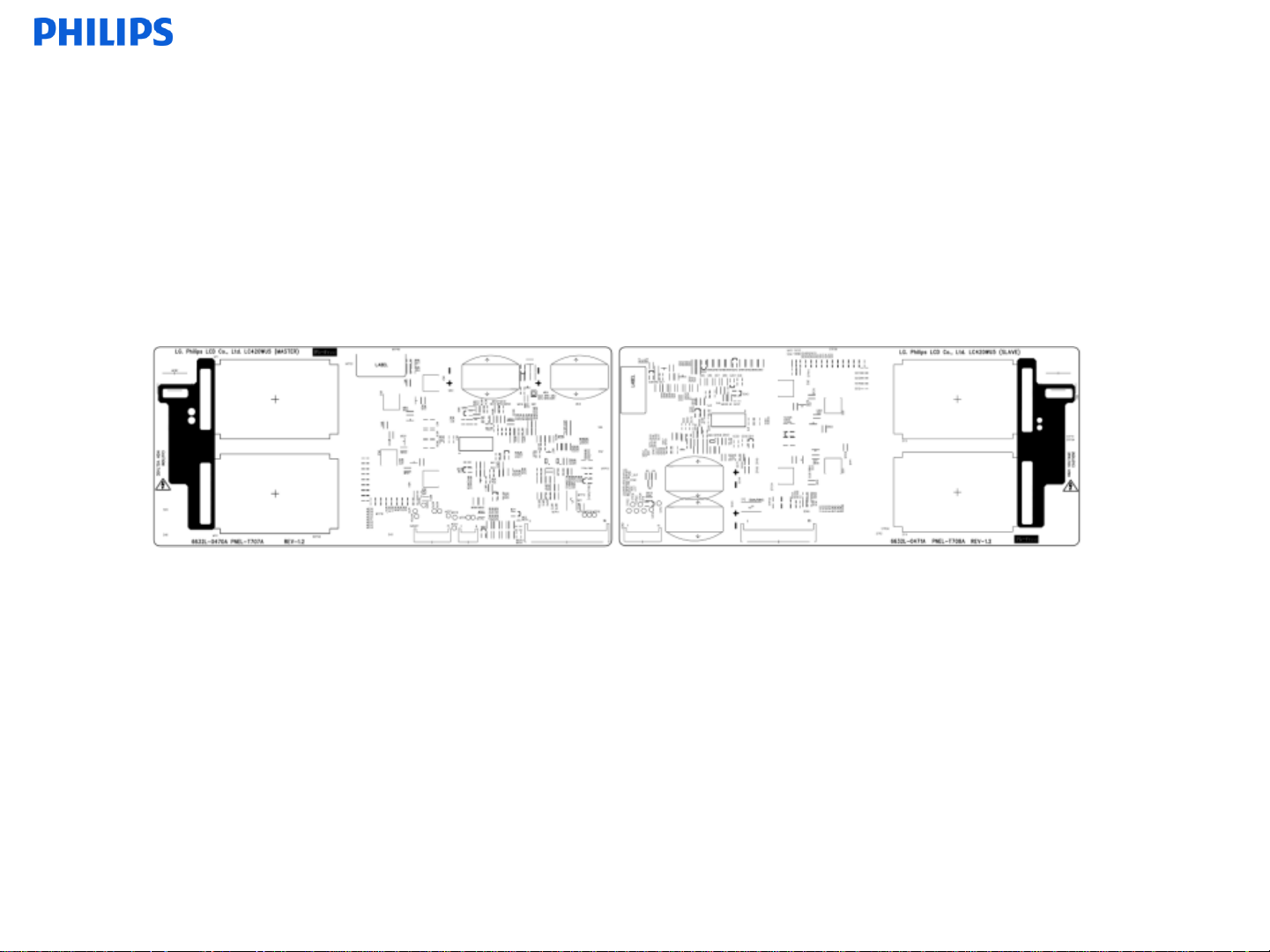
Confirm Inverter model name:
•PNEL-T707A(MASTER),
•PNEL-T708A(SLAVE).
REMARK 1
• It does not matter if the zener diode (modification “I”) exists or not for
inverter modification “II”.
3
Page 4
SCC_73709
STEP 2.1
Cut tracks:
- Cut the SW1 & SW2 tracks on both inverters.
- Confirm that there are no short circuits with metal
pieces of tracks, and there is no damage to other tracks !
PNEL-T707A
PNEL-T708A
4
Page 5
SCC_73709
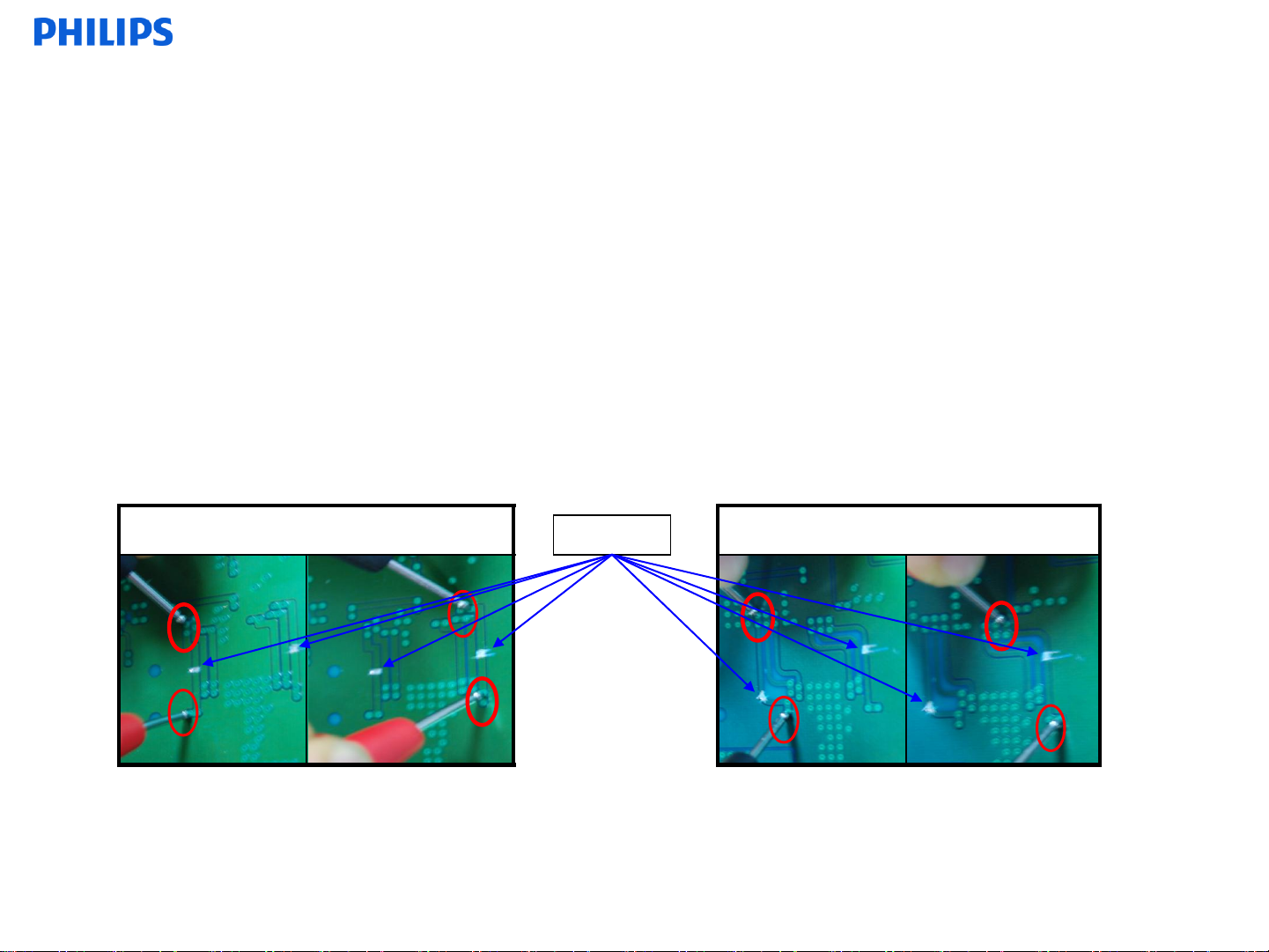
STEP 2.2
1. Check the secure cut line (SW1 & SW2) by visual inspection first:
Visual inspection to verify if cut well and not damaged.
2. Check the resistance between two ‘via’ holes of the cut SW line:
Measure the resistance of the cutted SW1 & SW2 line through „via‟ holes
with a DVM (Digital Volt Meter).
Measure Point (Master) Measure Point (Slave)
Case 1 > Several tens of kΩ: Line cut well.
Case 2 > under 1 Ω: Line short.
※ After attaching the resistor, the resistance should be 4.2 ~ 5.2 Ω.
Cut Mark
5
Page 6

SCC_73709
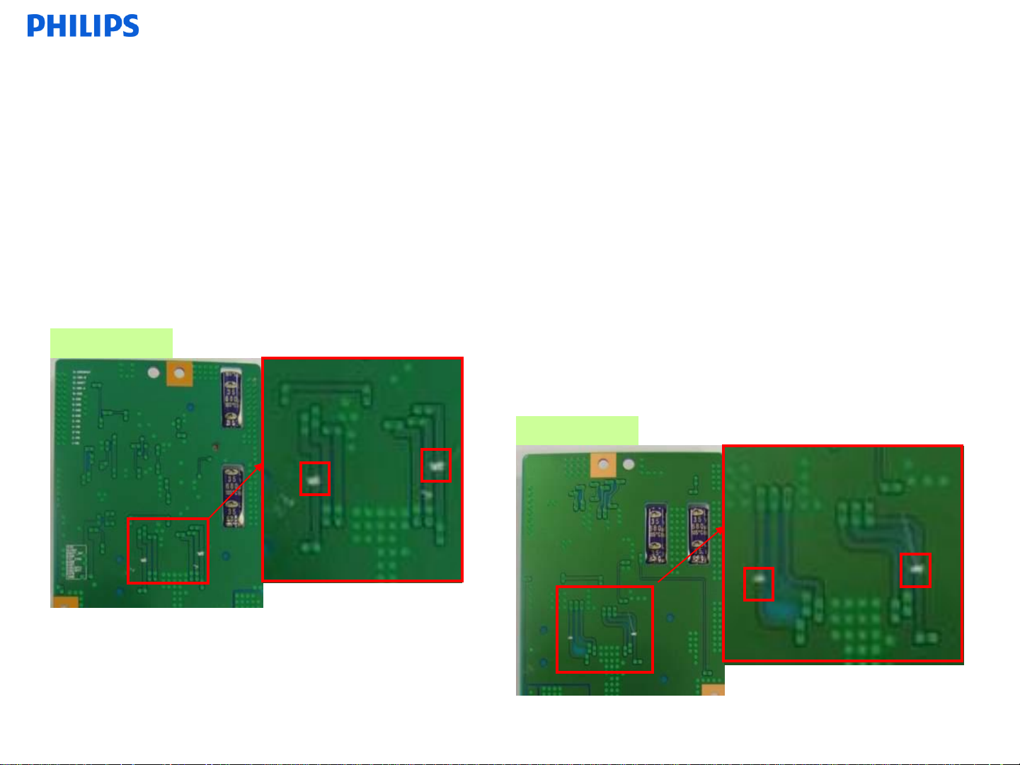
STEP 2.3
Check pattern damage of parallel tracks
Cut Mark
PNEL-T707A PNEL-T708A
GND
Cut mark
GND
GND
SW2 Pattern
HN2 Pattern
SW1 Pattern
HN1 Pattern
GND
SW1 Pattern
HN1 Pattern
Case study for pattern damage of parallel tracks
Parallel tracks of SW line are HN1, HN2 and GND tracks.
- Case1> If cut the HN track by mistake Cause of Inverter malfunction.
Check : HN line‟s resistance should be under 0.5Ω when measured with DVM (resistance b.t.w. via holes of HN line).
- Case2> Damage on GND track by mistake No affect to Inverter function.
No damage on GND function because GND track is spread widely.
SW2 Pattern
HN2 Pattern
6
Page 7

SCC_73709
REMARK 2
• The kit of components can include the following resistors:
4 x DIP type resistors (4.7 Ω) with shrink tube (20 mm)
then go to step 3.1 and 3.2
OR
20mm
4 x SMD type resistors (4.7 Ω)
then go to step 3.3
7
Page 8

SCC_73709
STEP 3.1
Solder resistors on board PNEL-T708A:
- Remove the coating/varnish on solder point to reveal the copper pad.
- Solder resistor (DIP type resistors (4.7 Ω) with shrink tube (20 mm)) on solder points (red marks).
PNEL-T708A PNEL-T708A
8
Page 9

SCC_73709
STEP 3.2
Solder resistors on board PNEL-T707A:
- Remove the coating/varnish on solder point to reveal the copper pad.
- Solder resistor (DIP type resistors (4.7 Ω) with shrink tube (20 mm)) on solder points (red marks).
PNEL-T707A PNEL-T707A
9
Page 10

SCC_73709
REMARK 3
Front side of reworked inverter (DIP type resistor):
DIP type resistor (Front)
Side view dimension of implemented inverter
Take care that the height of the DIP type resistor is below the height of the transformer
because of the metal shielding on the inverter boards.
Shield Cover
3.5mm
Cover Bottom
11mm
Cap.
8mm
Resistor
1mm
Trans.
10.1mm
3.5mm
10
Page 11

SCC_73709
STEP 3.3
Solder SMD resistors on board PNEL-T707A and PNEL-T708A:
- Remove the coating/varnish on solder points to reveal the copper.
- Solder SMD resistor on created solder pads (red marks).
11
Page 12

SCC_73709
STEP 3.4
Solder capacitor (MLCC) on PNEL-T707A and PNEL-T708A:
-Solder capacitor MLCC (100 pF) on blue indicated position.
MLCC position
PNEL-T707A PNEL-T708A
PNEL-T707A PNEL-T708A
12
Page 13

SCC_73709
STEP 3.5
Solder zener diode (TVS) on PNEL-T707A and PNEL-T708A:
- Solder zener diode TVS (33 V) on red indicated position.
Classification Indication Attachment
Polarity Band mark on body Place band mark on assigned position
TVS position
PNEL-T707A PNEL-T708A
Non polarity No mark No need to distinguish the TVS direction
Polarity : Band mark position
Non-Polarity: No placing direction
PNEL-T707A PNEL-T708A
13
Page 14

14
 Loading...