

Page 1

SERVICE MANUAL
SERVICE MANUAL
CAUTION
BEFORE SERVICING THE UNIT, READ THE “SAFETY PRECAUTIONS”
IN THIS MANUAL.
Internal Use Only
Mini Hi-Fi AUDIO
APRIL, 2016P/NO : AFN77483239
MODEL: OM7560
MODEL: OM7560
Page 2

CONTENTS
SECTION 1 ........ GENERAL
SECTION 2 ........ CABINET & MAIN CHASSIS
SECTION 3 ........ ELECTRICAL
SECTION 4 ........ MECHANISM (DM19AC)
SECTION 5 ........ REPLACEMENT PARTS LIST
1-1
Page 3

SECTION 1
SUMMARY
CONTENTS
SERVICING PRECAUTIONS ............................................................................................................................ 1-3
ESD PRECAUTIONS ......................................................................................................................................... 1-5
HIDDEN KEY MODE ......................................................................................................................................... 1-6
SERVICE INFORMATION FOR EEPROM ........................................................................................................ 1-7
PROGRAM DOWNLOAD GUIDE ...................................................................................................................... 1-8
SPECIFICATIONS ........................................................................................................................................... 1-11
1-2
Page 4
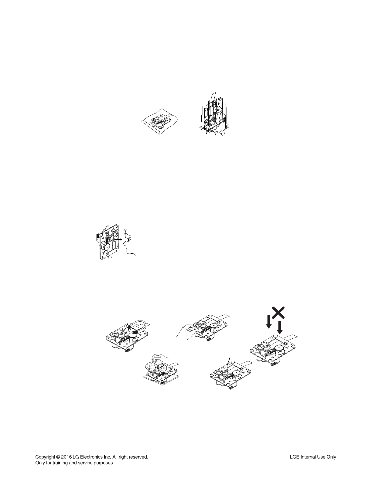
1-3
NOTES REGARDING HANDLING OF THE PICK-UP
1. Notes for transport and storage
1) The pick-up should always be left in its conductive bag until immediately prior to use.
2) The pick-up should never be subjected to external pressure or impact.
2. Repair notes
1) The pick-up incorporates a strong magnet, and so should never be brought close to magnetic materials.
2) The pick-up should always be handled correctly and carefully, taking care to avoid external pressure and
impact. If it is subjected to strong pressure or impact, the result may be an operational malfunction and/or
damage to the printed-circuit board.
3) Each and every pick-up is already individually adjusted to a high degree of precision, and for that reason
the adjustment point and installation screws should absolutely never be touched.
4) Laser beams may damage the eyes!
Absolutely never permit laser beams to enter the eyes!
Also NEVER switch ON the power to the laser output part (lens, etc.) of the pick-up if it is damaged.
5) Cleaning the lens surface
If there is dust on the lens surface, the dust should be cleaned away by using an air bush (such as used
for camera lens). The lens is held by a delicate spring. When cleaning the lens surface, therefore, a cotton swab should be used, taking care not to distort lens.
6) Never attempt to disassemble the pick-up.
Spring has excess pressure. If the lens is extremely dirty, apply isopropyl alcohol to the cotton swab.
(Do not use any other liquid cleaners, because they will damage the lens.) Take care not to use too much
of this alcohol on the swab, and do not allow the alcohol to get inside the pick-up.
Storage in conductive bag
Drop impact
NEVER look directly at the laser beam, and don’t allow
contact with fingers or other exposed skin.
Magnet
How to hold the pick-up
Conductive Sheet
Cotton swab
Pressure
Pressure
SERVICING PRECAUTIONS
Page 5
NOTES REGARDING COMPACT DISC PLAYER REPAIRS
1. Preparations
1) Compact disc players incorporate a great many ICs as well as the pick-up (laser diode). These components
are sensitive to, and easily affected by, static electricity. If such static electricity is high voltage, components
can be damaged, and for that reason components should be handled with care.
2) The pick-up is composed of many optical components and other high-precision components. Care must be
taken, therefore, to avoid repair or storage where the temperature or humidity is high, where strong magnetism is present, or where there is excessive dust.
2. Notes for repair
1) Before replacing a component part, first disconnect the power supply lead wire from the unit
2) All equipment, measuring instruments and tools must be grounded.
3) The workbench should be covered with a conductive sheet and grounded.
When removing the laser pick-up from its conductive bag, do not place the pick-up on the bag. (This is
because there is the possibility of damage by static electricity.)
4) To prevent AC leakage, the metal part of the soldering iron should be grounded.
5) Workers should be grounded by an armband (1 M)
6) Care should be taken not to permit the laser pick-up to come in contact with clothing, in order to prevent
static electricity changes in the clothing to escape from the armband.
7) The laser beam from the pick-up should NEVER be directly facing the eyes or bare skin.
Resistor
(1 M)
Conductive
Sheet
Resistor
(1 M)
Armband
1-4
Page 6
1-5
Electrostatically Sensitive Devices (ESD)
Some semiconductor (solid state) devices can be damaged easily by static electricity. Such components
commonly are called Electrostatically Sensitive Devices (ESD). Examples of typical ESD devices are integrated
circuits and some field-effect transistors and semiconductor chip components. The following techniques should
be used to help reduce the incidence of component damage caused by static electricity.
1. Immediately before handling any semiconductor component or semiconductor-equipped assembly, drain off
any electrostatic charge on your body by touching a known earth ground. Alternatively, obtain and wear a
commercially available discharging wrist strap device, which should be removed for potential shock reasons
prior to applying power to the unit under test.
2. After removing an electrical assembly equipped with ESD devices, place the assembly on a conductive surface
such as aluminum foil, to prevent electrostatic charge buildup or exposure of the assembly.
3. Use only a grounded-tip soldering iron to solder or unsolder ESD devices.
4. Use only an anti-static solder removal device. Some solder removal devices not classified as "anti-static" can
generate electrical charges sufficient to damage ESD devices.
5. Do not use freon-propelled chemicals. These can generate electrical charges sufficient to damage ESD
devices.
6. Do not remove a replacement ESD device from its protective package until immediately before you are
ready to install it. (Most replacement ESD devices are packaged with leads electrically shorted together by
conductive foam, aluminum foil or comparable conductive materials).
7. Immediately before removing the protective material from the leads of a replacement ESD device, touch the
protective material to the chassis or circuit assembly into which the device will by installed.
CAUTION : BE SURE NO POWER IS APPLIED TO THE CHASSIS OR CIRCUIT, AND OBSERVE ALL OTHER
SAFETY PRECAUTIONS.
8. Minimize bodily motions when handing unpackaged replacement ESD devices. (Otherwise harmless motion
such as the brushing together of your clothes fabric or the lifting of your foot from a carpeted floor can generate
static electricity sufficient to damage an ESD device).
CAUTION. GRAPHIC SYMBOLS
THE LIGHTNING FLASH WITH APROWHEAD SYMBOL. WITHIN AN EQUILATERAL TRIANGLE, IS
INTENDED TO ALERT THE SERVICE PERSONNEL TO THE PRESENCE OF UNINSULATED
“DANGEROUS VOLTAGE” THAT MAY BE OF SUFFICIENT MAGNITUDE TO CONSTITUTE A RISK OF
ELECTRIC SHOCK.
THE EXCLAMATION POINT WITHIN AN EQUILATERAL TRIANGLE IS INTENDED TO ALERT THE
SERVICE PERSONNEL TO THE PRESENCE OF IMPORTANT SAFETY INFORMATION IN SERVICE
LITERATURE.
ESD PRECAUTIONS
Page 7

1-6
HIDDEN KEY MODE
Push both Front key and RCU key to activate it for 5 seconds.
1. Disc Lock On/Off (CD Function Only Active)
Front Key : STOP
RCU Key :STOP
2. Check Version and Option code
Front Key : STOP
RCU Key : PLAY/PAUSE
You can change [Audio MCU Version <-> CD Controller Version <-> EEPROM Option] by SKIP+/-.
3. Clear EEPROM
Front Key : STOP
RCU Key : SKIP- (CD Model), 0 (DVD Model)
4. Edit EEPROM
Front Key : STOP
RCU Key : SKIP+
You can change the digit of option by SKIP+/-.
You can edit 0~f by REPEAT or PLAY/PAUSE key.
5. Measure Mode (Bypass)
Front Key : STOP
RCU Key : 8
HW output measure
Page 8
POWER ON
VFD “NO DISC” status
It is possible at any function.
(ex. It is possible at VFD “NO USB” status, too.)
This is an example.
Front ‘Stop’ + Remote control ‘ ’
push same timing during 5 s
FLD “OP00-…..”
Move to appropriate position
And make changes with remote control
“ , , , REPEAT” key.
Press ‘Stop’ Key
VFD “WRITE OK”
Front ‘Stop’ + Remote control ‘ ’
push same timing during 5 s
VFD “E2P CLR”
Completed
1-7
SERVICE INFORMATION FOR EEPROM
/
Page 9

1. AUDIO PROGRAM
Download program file name must be MICOM_OM7560_YYMMDDX.HEX
If security program(Water Wall) is activated on PC, you must save the file to the USB storage device
and disable the security software, then download the file to your set.
Downloading file proceeds in the same way at USB1 function and USB2 function.
Caution:
When downloading the file, you should neither unplug the USB device, change to the other function,
nor power off the device. USB device must be unplugged when the downloading process is completed.
ON VFD DISPLAY SCREEN
1) (Fast) Format USB device.
2) Copy Firmware file to USB device.
NO USB
Insert USB device at USB function.
SEARCH
MICOM UP
FINISH
AUTO POWER OFF
1-8
PROGRAM DOWNLOAD GUIDE
Page 10
2. CD PROGRAM
Download program file name must be HG690_OM7560_YYMMDDX.bin
If security program(Water Wall) is activated on PC, you must save the file to the USB storage device
and disable the security software, then download the file to your set.
Downloading file proceeds in the same way at USB1 function and USB2 function.
Caution:
When downloading the file, you should neither unplug the USB device, change to the other function,
nor power off the device. USB device must be unplugged when the downloading process is completed.
ON VFD DISPLAY SCREEN
1) (Fast) Format USB device.
2) Copy Firmware file to USB device.
NO USB
Insert USB device at USB function.
SEARCH
FIRMWARE
FINISH
AUTO POWER OFF
1-9
Page 11
3. EQ PROGRAM
Download program file name must be EQ_PRG.BIN
If security program(Water Wall) is activated on PC, you must save the file to the USB storage device
and disable the security software, then download the file to your set.
Downloading file proceeds in the same way at USB1 function and USB2 function.
Caution:
When downloading the file, you should neither unplug the USB device, change to the other function,
nor power off the device. USB device must be unplugged when the downloading process is completed.
ON VFD DISPLAY SCREEN
1) (Fast) Format USB device.
2) Copy Firmware file to USB device.
NO USB
Insert USB device at USB function.
SEARCH
EQ UP
FINISH
AUTO POWER OFF
1-10
Page 12

SPECIFICATIONS
1-11
• GENERAL
Power requirements Refer to the main label.
Power consumption Refer to the main label.
Dimensions (W x H x D) 330 x 815 x 302 mm
Net Weight (Approx.) 16.8 kg
Operating temperature 5 °C to 35 °C (41 °F to 95 °F)
Operating humidity 5 % to 90 %
Bus Power Supply (USB) 5 V 500 mA x 2
• INPUTS
AUX IN 2.0 Vrms (1 kHz, 0 dB), 75 Ω, RCA jack (L, R) x 1
PORT IN 1.2 Vrms (3.5 mm stereo jack)
• TUNER
FM Tuning Range 87.5 to 108.0 MHz or 87.50 to 108.00 MHz
• AMPLIFIER
Stereo mode 300 W + 300 W (4 Ω at 1 kHz, THD 10 %)
Front 300 W + 300 W (4 Ω at 1 kHz, THD 10 %)
Woofer 400 W (3 Ω at 200 Hz, THD 10 %)
• CD
Frequency Response 100 to 20 000 Hz
Signal-to-noise ratio 75 dB
Dynamic range 75 dB
• Design and specifications are subject to change without notice.
Page 13

1-12
Page 14

SECTION 2
CABINET & MAIN CHASSIS
CONTENTS
DISASSEMBLY INSTRUCTIONS ..................................................................................................................... 2-2
EXPLODED VIEWS ........................................................................................................................................... 2-3
1. CABINET AND MAIN FRAME SECTION ................................................................................................. 2-3
2. MECHANISM DECK SECTION (DM19AC) .............................................................................................. 2-5
3. PACKING ACCESSORY SECTION ......................................................................................................... 2-7
2-1
Page 15

2-2
DISASSEMBLY INSTRUCTIONS
Figure 2
Figure 1
2) To disassemble the Front Panel, remove the two screws and disassemble.
1) When disassembling the Frame Top, do not rotate and disassemble by pulling upwards.
Page 16
RMC
TOP
E
D
M
H
P
J
M
A
C
O
I
K
L
G
F
K
L
B
E
D
J
I
F
G
N
N
P
H
C
A
B
O
MAIN
SMPS
260L
476
475
251
255
254
464
252
464
253
256
258
259
464
475
256
A50
475
270
475
A51
464
271
272
273
A41
475
475
A47
475
475
263
475
475
A46
275
264
476
475
260R
265
476
476
267
521
475
475
521
521
262
475
269
266
266
266
475
274
A42
475
475
270
257
CABLE4
CABLE1
CABLE3
CABLE2
A44
A43
464
A60
EXPLODED VIEWS
1. CABINET AND MAIN FRAME SECTION
NOTES) THE EXCLAMATION POINT WITHIN AN
EQUILATERAL TRIANGLE IS INTENDED
TO ALERT THE SERVICE PERSONNEL
TO THE PRESENCE OF IMPORTANT
SAFETY INFORMATION IN SERVICE
LITERATURE.
Page 17

1439
A001
1002
1005
1001
1003
1004
1026
1043
A005
1016
1013
1015
1020
1439
1018
1019
1012
A006
1045
1049
1437
1437
1024
1024
1024
1024
1437
1011
1030
2. MECHANISM DECK SECTION (DM19AC)
Page 18
3. PACKING ACCESSORY SECTION
801 Owner’s manual
803 Packing
803 Packing
802 Box
804 Bag
808 Batteries
825 FM antenna
900 Remote control
300 Power Cord
Optional Part
Page 19
2-8
Page 20

SECTION 3 ELECTRICAL
CONTENTS
ONE POINT REPAIR GUIDE ............................................................................................................................ 3-2
1. NO POWER ............................................................................................................................................ 3-2
2. NO BOOTING WHEN POWER ON THE SET........................................................................................ 3-3
3. VFD IS NOT DISPLAYED WHEN POWER ON THE SET ..................................................................... 3-4
4. NO BOOTING (IN CD/USB FUNCTION) ................................................................................................ 3-5
5. NO OPERATION OF MD ........................................................................................................................ 3-9
6. NO SOUND ........................................................................................................................................... 3-14
ELECTRICAL TROUBLESHOOTING GUIDE ................................................................................................. 3-22
1. POWER (SMPS) ................................................................................................................................... 3-22
2. MCS PART CHECK .............................................................................................................................. 3-25
3. FLD DISPLAY CHECK ......................................................................................................................... 3-26
4. PWM MODULATION CHECK ............................................................................................................... 3-27
5. POWER AMP PART CHECK ............................................................................................................... 3-28
6. TUNER / AUX FUNCTION CHECK ...................................................................................................... 3-29
7. TUNER FUNCTION CHECK................................................................................................................. 3-30
8. CD FUNCTION CHECK ........................................................................................................................ 3-31
9. DOUBLE USB FUNCTION ................................................................................................................... 3-32
WAVEFORMS OF MAJOR CHECK POINT .................................................................................................... 3-33
1. DSP (IC501) .......................................................................................................................................... 3-33
2. SDRAM (IC502) .................................................................................................................................... 3-34
3. SERVO (IC401) ..................................................................................................................................... 3-35
4. MOTOR DRIVER (IC400) ..................................................................................................................... 3-36
5. ADC (IC201) .......................................................................................................................................... 3-37
6. USB (CN502) ........................................................................................................................................ 3-37
7. BLUETOOTH (CN504) .......................................................................................................................... 3-38
WIRING DIAGRAM .......................................................................................................................................... 3-39
BLOCK DIAGRAMS ........................................................................................................................................ 3-41
1. SYSTEM BLOCK DIAGRAM ................................................................................................................ 3-41
2. POWER BLOCK DIAGRAM ................................................................................................................. 3-43
3. AUDIO PATH BLOCK DIAGRAM ......................................................................................................... 3-45
CIRCUIT DIAGRAMS ...................................................................................................................................... 3-47
1. SMPS CIRCUIT DIAGRAM .................................................................................................................. 3-47
2. MAIN - CD DSP CIRCUIT DIAGRAM ................................................................................................... 3-49
3. MAIN - SUB MICOM CIRCUIT DIAGRAM ........................................................................................... 3-51
4. MAIN - POWER PART CIRCUIT DIAGRAM ........................................................................................ 3-53
5. MAIN - ADC/ DAC/ PWM CIRCUIT DIAGRAM .................................................................................... 3-55
6. MAIN - RF SERVO CIRCUIT DIAGRAM .............................................................................................. 3-57
7. MAIN - PWM/ AMP CIRCUIT DIAGRAM .............................................................................................. 3-59
8. MAIN - FAN & LED LIGHTING CIRCUIT DIAGRAM ........................................................................... 3-61
9. TOP FRONT CIRCUIT DIAGRAM ........................................................................................................ 3-63
10. JACK/ RMC CIRCUIT DIAGRAM ......................................................................................................... 3-65
11. FRONT LED CIRCUIT DIAGRAM ........................................................................................................ 3-67
CIRCUIT VOLTAGE CHART ........................................................................................................................... 3-69
1. IC INPUT VOLTAGE ............................................................................................................................. 3-69
2. CAPACITOR VOLTAGE ....................................................................................................................... 3-70
3. CONNECTOR VOLTAGE ..................................................................................................................... 3-71
PRINTED CIRCUIT BOARD DIAGRAMS
....................................................................................................... 3-75
1. SMPS P.C.BOARD ............................................................................................................................... 3-75
2. MAIN P.C.BOARD ................................................................................................................................ 3-77
3. TOP FRONT P.C.BOARD .................................................................................................................... 3-81
4. JACK/ RMC P.C.BOARD ...................................................................................................................... 3-85
5. FRONT LED P.C.BOARD ..................................................................................................................... 3-85
3-1
Page 21
3-2
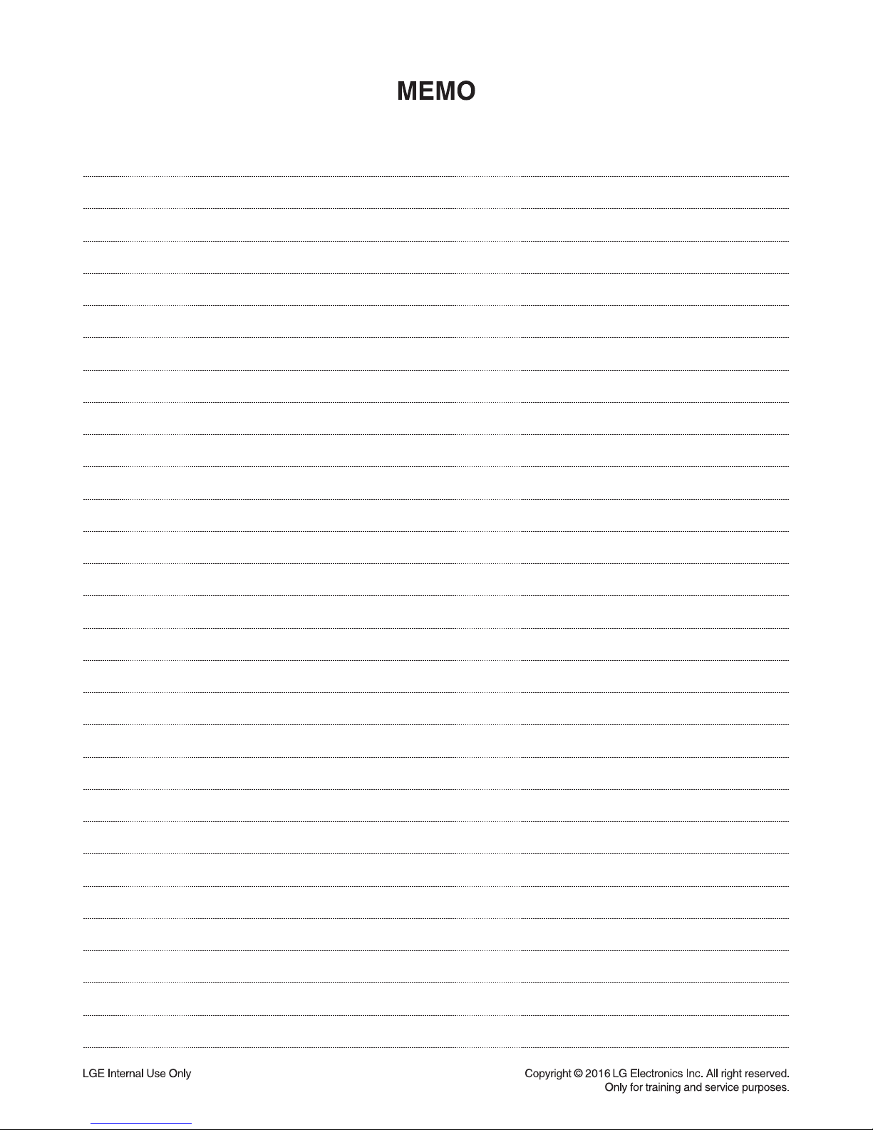
ONE POINT REPAIR GUIDE
1. NO POWER
If the unit doesn’t work by no power problem, repair the set according to the following guide.
1-1. FUSE/ THERMISTOR/ BRIDGE DIODE
1-1-1. Solution
Please check and replace F901, TH901 or TH903, BD901 on SMPS board.
1-1-2. How to troubleshoot (Countermeasure)
1) Check if the fuse F901 is open or short-circuit.
2) Check if the NTC thermistor TH900 or TH903 is normal or open.
3) Check if the bridge diode BD901 is short-circuit by over current with a digital multi-meter.
1-1-3. Service hint (Any picture/ Remark)
< F901 >
If F901 is not short-circuit,
replace it with a same
specifi cations one.
< BD901 >
If BD901 is short-circuit,
replace it with a new one.
<TH901 or TH903 >
If TH901 or TH903 is open,
replace it with a new one.
Page 22
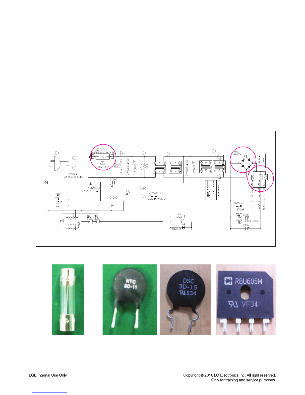
3-3
ONE POINT REPAIR GUIDE
NO POWER
If the unit doesn’t work by no PVDD problem, repair the set according to the following guide.
1-2. FUSE/ FET
1-2-1. Solution
Please check and replace F901, Q901 on SMPS board.
1-2-2. How to troubleshoot (Countermeasure)
1) Check if the fuse F901 is open or short-circuit.
2) Check the anode-cathod voltage of D951 with a digital multi-meter, it is normally 0.2 ~ 0.3 V.
If it doesn’t have any voltage, it’s destroyed. Replace it with a new one.
1-2-3. Service hint (Any picture/ Remark)
< SMPS circuit >
Page 23
3-4
ONE POINT REPAIR GUIDE
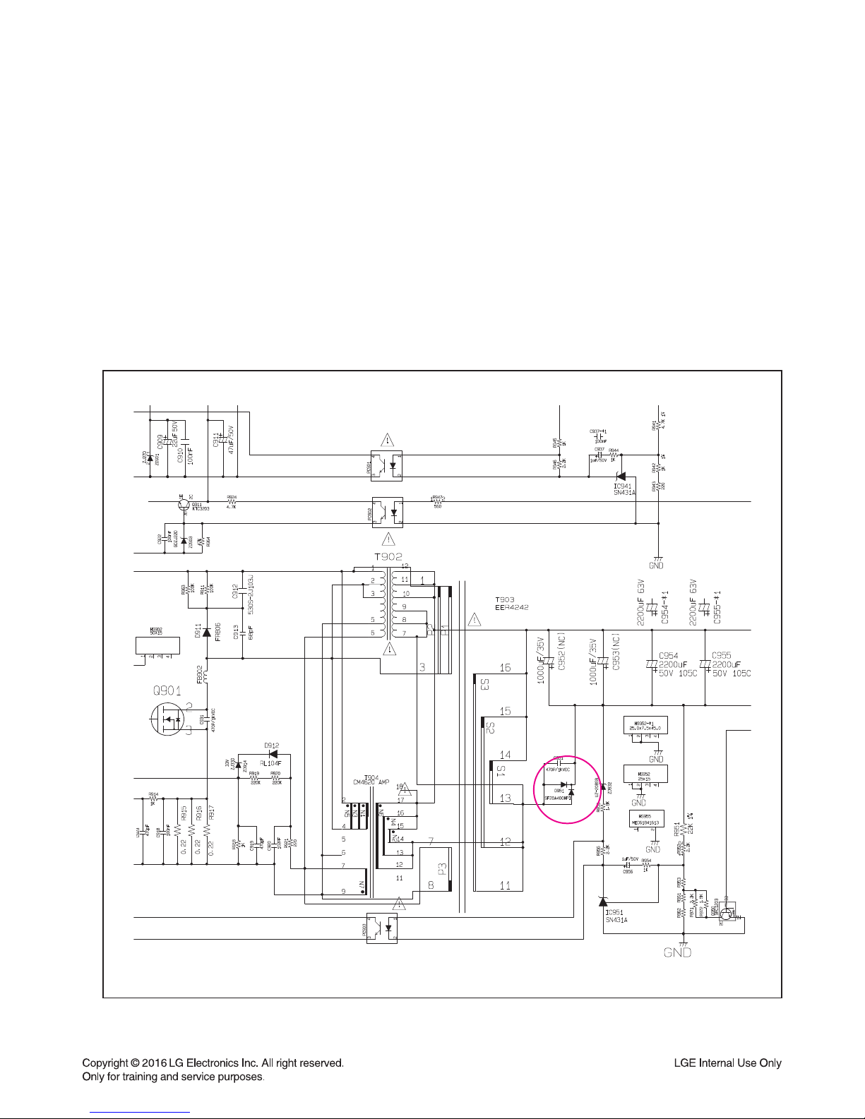
2. NO BOOTING WHEN POWER ON THE SET
The set doesn’t work when press the power button on the top board or the remote control.
2-1. IC501
2-1-1. Solution
Replace IC501 on MAIN board.
2-1-2. How to troubleshoot (Countermeasure)
1) Check the +12 VA (CN202) and 3.3VA (IC503) in standby mode.
If there is no 12 VA, check the SMPS and if doesn’t appear 3.3 VA, check IC503.
2) Check +12 VA, +5.1 VA, 3.3 VA, DVCC_5V and DVCC_3.3V when power on the set.
-
If the set doesn’t work regardless of what the KEY1 changes high to low while pressing the power button.
X500 and X501 work normally but, if you can not power on the set, replace the IC501 with a new one
on the main board.
2-1-3. Service hint (Any picture/ Remark)
< MAIN board top view >
< MAIN board bottom view >
X500
X500
(24 MHz)
(24 MHz)
X501
X501
(32.768 kHz)
(32.768 kHz)
KEY1
KEY1
(R518)
(R518)
PWR_CTRL
PWR_CTRL
R559
R559
Page 24

3-5
ONE POINT REPAIR GUIDE
3. VFD IS NOT DISPLAYED WHEN POWER ON THE SET
When power on the set, any icons or characters on VFD are not displayed.
3-1. VFD (VFD301)
3-1-1. Solution
Please check and replace VFD301 on TOP FRONT board.
3-1-2. How to troubleshoot (Countermeasure)
1) Check if VFD_12V, DVCC_3.3V and VCC_5V are output from SMPS to VFD via the main board.
2) Check if the IC501 outputs VFD_CLK, VFD_STB, and VFD_DAT to the top board.
3) Check if the VFD grid current amplifier circuit on the top board.
Check the drive signal to the transistor’s(Q801,2) base.
If the control signals from VFD (DGND, VDD) isn’t output, replace VFD with a new one.
3-1-3. Service hint (Any picture/ Remark)
R812(TP 841)
Q801 Emitte r
about
30 Vp-p
< TOP FRONT circuit >
< Waveform of the grid current driver>
Page 25

3-6
ONE POINT REPAIR GUIDE
4. NO BOOTING (IN CD/USB FUNCTION)
After you turn on power key and displayed message in the following order (HELLO VOL XX
CD or USB) on VFD, it will not display other message on VFD, and it will not boot-up normally.
4-1. NO DVCC_3.3V, 1.2 VA
4-1-1. Solution
Please check and replace IC202, IC205 on MAIN board.
4-1-2. How to troubleshoot (Countermeasure)
1) Check Voltage of IC202 pin3 on MAIN board.
If IC202 pin3 (about 5.1 V) & pin1 Input 12 VA doesn’t come out, check +12 VA from SMPS board.
2) If IC202 pin3 (about 5.1 V) is normal, check voltage of IC205 pin3 (about 1.2 VA), pin6 (about 3.3 VA).
If IC205 pin3 (about 1.2 VA), pin6 (about 3.3 VA) doesn’t come out, check R253, R254, R256 and R260, R261, R262.
If there’s no defective component then replace IC205.
3) PWR_CTRL is high, check R512 and if there’s no defective component then replace IC505.
PWR_CTRL (IC505 pin3) is high (about 3.2 V)
If PWR_CTRL isn’t high, check pin D11 of IC501 & R512, R513
4) If PWR_CTRL is high, check R559 and if there’s no defective component then replace IC505.
4-1-3. Service hint (Any picture/ Remark)
< MAIN board top view >
< MAIN board bottom view >
IC505
IC505
IC202
IC202
IC205
IC205
Page 26

3-7
ONE POINT REPAIR GUIDE
NO BOOTING (IN CD/USB FUNCTION)
After you turn on power key and displayed message in the following order (HELLO VOL XX
CD or USB) on VFD, it will not display other message on VFD, and it will not boot-up normally.
4-2. CRYSTAL (X500)
4-2-1. Solution
Replace X500 on MAIN board.
4-2-2. How to troubleshoot (Countermeasure)
1) If 3.3 VA & 1.2 VA is normal, check reset ‘High’ of IC501 pin T12 on MAIN board.
If MAIN_RESET isn’t high, check MICOM (IC101) pin40.
2) If MAIN_RESET is high, check the soldering status of 24 MHz crystal (X500).
3) If the crystal (X500) doesn’t oscillate, check R508, C502, C503 around crystal (X500).
If there’s no defective component, then replace X500.
4-2-3. Service hint (Any picture/ Remark)
X
XI
XO
X500
< Signal waveform >
< MAIN board top view >
IC501
IC501
X500
X500
Page 27

3-8
ONE POINT REPAIR GUIDE
NO BOOTING (IN CD/USB FUNCTION)
After you turn on power key and displayed message in the following order (HELLO VOL XX
CD or USB) on VFD, it will not display other message on VFD, and it will not boot-up normally.
4-3. SERIAL FLASH (IC503)
4-3-1. Solution
Please check and replace IC503 on MAIN board.
4-3-2. How to troubleshoot (Countermeasure)
1) If the crystal (X500) does oscillate, check serial flash (IC503) on MAIN board.
Check pin8 (VCC), pin6 (CLK), pin1 (CS), pin2 (DO), pin5 (DI) of below waveform.
2) If pin1, 2, 5, 6 doesn’t come out, check registers (R563, R564, R534, R535, R536, R5E4) of IC503.
If registers of IC503 is OK, then replace IC503. (it need to download program.)
3) After change IC503, if It is still not below waveform, check IC501 (DSP IC).
4-3-3. Service hint (Any picture/ Remark)
VCC
CLK
DO
CS#
< Signal waveform >
< MAIN board bottom view >
IC503
IC503
Page 28

3-9
ONE POINT REPAIR GUIDE
5. NO OPERATION OF MD
When no sound output in the CD function, you can not listen to music reading data from a CD
disc if the servo motors in MD don’t work. This step is for checking the SPINDLE MOTOR among
them.
5-1. SPINDLE MOTOR
5-1-1. Solution
Replace IC400 on MAIN board.
5-1-2. How to troubleshoot (Countermeasure)
1) Check the SPDO signal from pin16 of IC401.
If no signal, check DVCC_3.3V and DV 3.3V (RF) and X400.
2) Check the SPIN+ & SPIN- from IC400 to CN401 for driving SPINDLE motor. It is about 3.6 Vp-p.
If no signal, check M_5 V for IC400.
3) Check if the FFC cable is solidly connected between CN401 and MD.
4) Check the MD.
If the spindle motor is sort-circuit or has any trouble, it can not rotate CD discs.
Please check the function after changing another MD.
5-1-3. Service hint (Any picture/ Remark)
< Waveform of SP- & SP+
for driving SPINDLE motor >
< MAIN board top view >
SP+: pin18
SP+: pin18
SP-: pin19
SP-: pin19
IC400
IC400
Page 29

3-10
ONE POINT REPAIR GUIDE
NO OPERATION OF MD
When no sound output in the CD function, you can not listen to music reading data from a CD
disc if the servo motors in MD don’t work. This step is for checking the SLED MOTOR among
them.
5-2. SLED MOTOR
5-2-1. Solution
Replace IC400 on MAIN board.
5-2-2. How to troubleshoot (Countermeasure)
1) Check the SLDO signal from pin15 of IC401.
If no signal, check DVCC_3.3V and DV 3.3V(RF) and X400.
2) Check the SPED+ & SLED- from IC400 to CN401 for driving SPINDLE motor. It is about 2.9 Vp-p.
If no signal, check M_5 V for IC400.
3) Check if the FFC cable is solidly connected between CN401 and MD.
4) Check the MD.
If the spindle motor is sort-circuit or has any trouble, it can not rotate CD discs.
Please check the function after changing another MD.
5-2-3. Service hint (Any picture/ Remark)
< Waveform of SLED- & SLED+
for driving SLED motor >
SP-
SP+
< MAIN board top view >
SLED+: pin11
SLED+: pin11
SLED-: pin12
SLED-: pin12
IC400
IC400
Page 30

3-11
< Waveform
for driving tray open/ close motor >
MOT_ CL OSE
MOT_OP EN
LO+(RED)
LO-
ONE POINT REPAIR GUIDE
NO OPERATION OF MD
When no sound output in the CD function, you can not listen to music reading data from a CD
disc if the servo motors in MD don’t work. This step is for checking the TRAY OPEN / CLOSE
MOTOR among them.
5-3. TRAY OPEN/ CLOSE MOTOR
5-3-1. Solution
Replace IC400 on MAIN board.
5-3-2. How to troubleshoot (Countermeasure)
1) Check MOT_OPEN & MOT_CLOSE signals from pin P5, L4 of IC501 to IC400.
If no signal, check M_5V to IC400.
2) Check LOAD± from IC400 to CN401 for driving the tray open / close motor. It is about 3.85 Vp-p.
If no signal, check M_5V to IC400. If it has any trouble, replace it with a new one.
3) Check if the FFC cable is solidly connected between CN401 and MD.
4) Check the MD.
If the tray motor is sort-circuit or has any trouble, it can not open or close the tray.
Please check the function after changing another MD.
5-3-3. Service hint (Any picture/ Remark)
< MAIN board top view >
MOT_CLOSE: pin6
MOT_CLOSE: pin6
MOT_OPEN: pin7
MOT_OPEN: pin7
LOAD+: pin9
LOAD+: pin9
LOAD-: pin10
LOAD-: pin10
IC400
IC400
Page 31

3-12
ONE POINT REPAIR GUIDE
NO OPERATION OF MD
When no sound output in the CD function, you can not listen to music reading data from a CD
disc if the pickup module in MD doesn’t work. This step is for checking the LASER TRACKING
ACTUATOR.
5-4. LASER TRACKING ACTUATOR
5-4-1. Solution
Replace IC400 on MAIN board.
5-4-2. How to troubleshoot (Countermeasure)
The tracking actuator makes the laser beam be positioned in the center of a track on CD disc.
1) Check the TRD signal from pin14 of IC401.
If no signal, check DVCC_3.3V & DV_3.3V (RF) and X400.
2) Check TR- & TR+ from IC400 to CN400 for driving the tracking actuator.
If no signal, check M_5V for IC400.
3) Check if the FFC cable is solidly connected between CN400 and MD.
4) Check the MD.
If the pickup module has any trouble, it can not move the laser beam on the left or right side.
Please check the function after changing another MD.
5-4-3. Service hint (Any picture/ Remark)
< Waveform of TR±
for driving tracking actuator >
< MAIN board top view >
TR+: pin16
TR+: pin16
TR-: pin15
TR-: pin15
IC400
IC400
Page 32

3-13
ONE POINT REPAIR GUIDE
NO OPERATION OF MD
When no sound output in the CD function, you can not listen to music reading data from a CD
disc if the pickup module in MD doesn’t work. This step is for checking the LASER FOCUSING
ACTUATOR.
5-5. LASER FOCUSING ACTUATOR
5-5-1. Solution
Replace IC400 on MAIN board.
5-5-2. How to troubleshoot (Countermeasure)
The focusing actuator makes the laser beam keep a regular interval with the surface of a CD disc.
1) Check the FDO signal from pin13 of IC401.
If no signal, check DVCC_3.3 & DV_3.3V(RF) and X400.
2) Check F- & F+ from IC400 to CN400 for driving the focusing actuator.
If no signal, check M_5V for IC400.
3) Check if the FFC cable is solidly connected between CN400 and MD.
4) Check the MD.
If the pickup module has any trouble, it can not move the laser beam on the top or bottom side.
Please check the function after changing another MD.
5-5-3. Service hint (Any picture/ Remark)
< Waveform of F±
for driving focusing actuator >
< MAIN board top view >
F+: pin14
F+: pin14
F-: pin13
F-: pin13
IC400
IC400
Page 33

3-14
ONE POINT REPAIR GUIDE
6. NO SOUND
There is no sound output by DIGITAL AUDIO AMP DAMAGE, repair the set according to the
following guide.
6-1. DIGITAL AUDIO AMP DAMAGE
6-1-1. Solution
Replace IC701, IC702 on MAIN board.
6-1-2. How to troubleshoot (Countermeasure)
1) Check PWM_FL±, PWM_FR± & PWM_SW± signals from IC601 to IC701 & 702 each input function.
If no signal, check if I2S audio signals are entered to IC601.
2) Check PVDD.
If PVDD is abnormal, check the SMPS.
3) Check AMP_12V for driving the gate of AMP IC.
a. All the powers are normal, but if AMP_12V is low, there is possible for AMP IC to be damaged.
b. Remove L701, L702, L703 and L704 one by one.
When removed a inductance, if AMP_12V is recovered, the IC connected to it was damaged.
c. Replace the IC with a new one.
4) Check the impedance between IC701/IC702_OUT_A/OUT_B & GND.
a. If the impedance is 0 Ω, the IC must be damaged.
b. After removing the heat sink, replace it with a new one.
6-1-3. Service hint (Any picture/ Remark)
< MAIN board top view >
IC701
IC701
L703
L703
L702
L702
L701
L701
L704
L704
IC702
IC702
IC601
IC601
Page 34

3-15
ONE POINT REPAIR GUIDE
NO SOUND
There is no sound output in the CD FUNCTION, repair the set according to the following guide.
6-2. CD FUNCTION
6-2-1. Solution
Replace IC501 on MAIN board.
6-2-2. How to troubleshoot (Countermeasure)
1) Check CD_BCK, CD_LRCK, & CD_DATA signals from IC501 to IC401.
If no signal, check if the RF & servo signals from MD is entered to IC401.
Refer to the “No operation of MD” guide on Item 5.
2) Check the following I2S signal flow. < I2S audio signal Interface >
- MCS_BCK : IC501_pin E1 --> IC601_pin23
- MCS_LRCK : IC501_pin D1 --> IC601_pin22 (44.1 kHz)
- MIX_DATA0_OUT : IC501_pin E2 --> IC601_pin24
- MCS_MCLK : IC501_pin D2 --> IC201_pin44
If there is any trouble, check the power for each IC.
The power is normal but, if the signal waveform to the IC is distorted or no signal,
replace it with a new one.
6-2-3. Service hint (Any picture/ Remark)
< Waveform of I2S audio interface signals >
< MAIN - CD DSP circuit >
< MAIN board top view >
IC501
IC501
R503
R503
Page 35

3-16
ONE POINT REPAIR GUIDE
NO SOUND
There is no sound output in the USB Function, repair the set according to the following guide.
6-3. USB FUNCTION
6-3-1. Solution
Replace IC204 on MAIN board.
6-3-2. How to troubleshoot (Countermeasure)
1) Check +5V_USB to USB board.
If the USB LED are turned on, the voltage is okay, if so not, check USB_5V to pin5, 6 of CN803.
2) Check USB D1± or USB D2± from MAIN board to TOP board.
a. Check 2.0_D1±signals(pin U7, U8 ) or 1.1_D1± signals(pin A7, A8 ) to IC501.
b. Check USB± signals to CN502(pin1, 2, 8, 9).
If there is any trouble, check the power for IC204.
The power is normal but, if the signal waveform to the IC is distorted or no signal,
replace it with a new one.
3) Check if “Digital audio AMP block” on item 6-1 is normal.
6-3-3. Service hint (Any picture/ Remark)
USB D-/D+ (CN502 pin1, 2 & pin8, 9)
< Waveform of USB D± signal >
D
D+
D-
< MAIN board top view >
CN502
CN502
Page 36

3-17
ONE POINT REPAIR GUIDE
NO SOUND
There is no sound output in the AUX Function, repair the set according to the following guide.
6-4. AUX FUNCTION
6-4-1. Solution
Replace IC201 on MAIN board.
6-4-2. How to troubleshoot (Countermeasure)
1) Check AUX_L/R signals to IC201 (pin23, 24).
2) Check if MCS_BCK, MCS_LRCK & MCS_MCLK are entered from IC501 to IC201.
3) Check if ADC_DATA is entered from IC201 to IC501.
If no signal, check DVCC_5V & DVCC_3.3V (ADC) for IC201. If is NG, replace it a new one.
4) Check the following I2S signal flow from IC501 to IC601. (Refer to Item 6-2.)
If there is any trouble, check the power for each IC. The power is normal but, if the signal waveform
to the IC is distorted or no signal, replace it with a new one.
5) Check if the digital audio AMP block is okay. Refer to “Digital Audio AMP” guide on Item 6-1.
If AMP is damaged, replace it with a new one.
6-4-3. Service hint (Any picture/ Remark)
< AUX function signal fl ow >
< MAIN board bottom view >
MCS_BCK: pin42
MCS_BCK: pin42
MCS_LRCK: pin43
MCS_LRCK: pin43
MCS_MLCK: pin44
MCS_MLCK: pin44
IC201
IC201
Page 37

3-18
ONE POINT REPAIR GUIDE
NO SOUND
There is no sound output in the TUNER function, repair the set according to the following guide.
6-5. TUNER FUNCTION
6-5-1. Solution
Replace IC201 on MAIN board.
6-5-2. How to troubleshoot (Countermeasure)
1) Check if TUNER_LR is entered from pin1, 3 of TU500 to IC201 (pin26, 27).
If no signals, check DVCC_3.3V for tuner power.
Check if the tuner control signals (CLK, DAT, CE, RST, SLT) are entered from IC501 to TU500.
If it doesn’t work, replace TUNER with a new one.
2) Check if MCS_BCK, MCS_LRCK, & MCS_MCLK are entered from IC501 to IC201.
3) Check if ADC_DATA is entered from IC201 to IC501.
If no signal, check DVCC_5V & DVCC_3.3V (ADC) for IC201. If is NG, replace it with a new one.
4) Check the following I2S audio signal flow from IC501 to IC601. (Refer to Item 6-2.)
If there is any trouble, check the power for each IC.
The power is normal but, if the signal waveform to the IC is distorted or no signal,
replace it with a new one.
5) Check if the digital audio AMP block is okay. Refer to “Digital Audio AMP” guide on Item 6-1.
If AMP is damaged, replace it with a new one.
6-5-3. Service hint (Any picture/ Remark)
< TUNER function signal fl ow >
< MAIN board bottom view >
TUNER_L: pin26
TUNER_L: pin26
TUNER_R: pin27
TUNER_R: pin27
IC201
IC201
Page 38

3-19
NO SOUND
There is no sound output in the PORTABLE Function, repair the set according to the following guide.
6-6. PORTABLE FUNCTION,
6-6-1. Solution
Replace IC201 on MAIN board.
6-6-2. How to troubleshoot (Countermeasure)
1) Check if PT_LR signals to IC201 (pin9, 10).
2) Check if MCS_BCK, MCS_LRCK, & MCS_MCLK are entered from IC501 to IC201.
3) Check if ADC_DATA is entered from IC201 to IC501.
If no signal, check DVCC_5V & DVCC_3.3V (ADC) for IC201. If is NG, replace it with a new one.
4) Check the following I2S audio signal flow from IC501 to IC601. (Refer to Item 6-2.)
If there is any trouble, check the power for each IC.
The power is normal but, if the signal waveform to the IC is distorted or no signal,
replace it with a new one.
5) Check if the digital audio AMP block is okay. Refer to “Digital Audio AMP” guide on Item 6-1.
If AMP is damaged, replace it with a new one.
6-6-3. Service hint (Any picture/ Remark)
< PORT. IN function signal fl ow >
ONE POINT REPAIR GUIDE
< MAIN board bottom view >
PT_L: pin9
PT_L: pin9
PT_R: pin10
PT_R: pin10
IC201
IC201
Page 39

3-20
ONE POINT REPAIR GUIDE
NO SOUND
There is no sound output in the MIC IN function, repair the set according to the following guide.
6-7. MIC IN function
6-7-1. Solution
Replace IC206 on MAIN board, ICA301 on TOP FRONT board.
6-7-2. How to troubleshoot (Countermeasure)
1) Check MIC_SI & MIC_S2 signal to pin5 & 6 of CN201.
If no signal, Check the signals to pin6 & 8 of CNA301 on the FRONT board.
Check if the signal is entered from pin 6 & 8 of CNA301 to pin 5 & 6 of CN201.
2) Check if MIC_SIG is entered from pin 6 of JK302 & JKA303 to pin2, 13 to ICA301 (PRE AMP).
3) Check if the amplified signal comes out from pin3 &12 of ICA301.
If no signal output, check DVCC_3.3V for ICA301, replace ICA301 with a new one if it has a problem.
4) Check if MCS_BCK, MCS_MLCK & MCS_LRCK is entered from IC501 to IC206.
Check if MIC_DATA_IN is entered from pin9 of IC206 to pin T1of IC501.
If no signal, check DVCC_5V & DVCC_3.3V for IC206.
If it is abnormal, change replace it a new one.
5) Check the following I2S signal flow from IC206 to IC501.
If there is any trouble, check the power for each IC.
If the signals are abnormal, replace it a new one.
6) Check if the digital audio AMP block is okay. Refer to “Digital Audio AMP” guide on item 6-1.
If AMP is damaged, replace it with a new one.
6-7-3. Service hint (Any picture/ Remark)
IC206
IC206
ADC/ MIC_DATA: pin9
ADC/ MIC_DATA: pin9
MCS_BCK: pin8
MCS_BCK: pin8
MCS_LRCK: pin7
MCS_LRCK: pin7
MCS_MCLK: pin6
MCS_MCLK: pin6
< MAIN board bottom view >
Page 40

3-21
ONE POINT REPAIR GUIDE
NO SOUND
There is no sound output in the Bluetooth function, repair the set according to the following guide.
6-8. BLUETOOTH FUNCTION
6-8-1. Solution
Replace IC501 on the MAIN board or bluetooth module on the FRONT Panel.
6-8-2. How to troubleshoot (Countermeasure)
1) Check BT_RX, BT_TX signal to pin6, 4 of CN504.
If no signal, check the signal to pin4, 6 and pin10 (BT_3.3V) of on the Bluetooth module
and cable connection state.
If there are no signal out from module, replace new module.
2) Check if BT_RX/TX is entered from pin6, 4 of CN504 to pin L1,K1 to IC501 (DSP).
3) Check if MCS_BCK, MCS_LRCK & MIX_DATA IN is entered from IC501 to IC601.
If no signal, check +3.3 VA & +1.2 VA for IC501.
If it is abnormal, change replace it a new one.
4) Check the following I2S signal flow from IC501 to IC601.
If there is any trouble, check the power for each IC.
If the signals are abnormal, replace it a new one.
5) Check if the digital audio AMP block is okay. Refer to “Digital Audio AMP” guide on item 6-1.
If AMP is damaged, replace it with a new one.
6-8-3. Service hint (Any picture/ Remark)
IC501
MLC3730
IC601
TPS5548DGG
PWM
MCS_BCK
MCS_LRCK
MIX_DATA0_OUT
TPS5631B
AMP
B/T Module
BT_RX,
BT_TX
< Bluetooth function signal fl ow >
< MAIN board bottom view >
Page 41

1. POWER (SMPS)
No 12 VA
YES
F901 normal?
Replace F901 (Use the same fuse).
YES
NO
BD901 normal?
Replace BD901.
YES
NO
TH901(TH903) normal?
Replace TH901.
YES
NO
Is Vcc
(10 V ~ 18 V) supplied to
IC901 pin7?
D902 normal?
YES
NO
Check or replace D902.
Is there
about 2.5 V at
IC941 pin1?
Replace IC941.
YES
YES
NO
D951 normal?
ZD932 normal?
Replace D951.
Replace ZD932.
YES
NO
NO
D933 normal?
Replace D933.
YES
NO
Power line of main PCB is short.
NO
3-22
ELECTRICAL TROUBLESHOOTING GUIDE
Page 42

No PVDD
YES
F901 normal?
Replace F901 (Use the same fuse).
YES
NO
BD901 normal? Replace BD901.
YES
YES
NO
TH901(TH903) normal?
Replace TH901.
YES
YES
NO
Is Vcc
(10 V ~ 18 V) supplied to
IC911 pin4?
D903 normal?
YES
NO
Check or replace D903.
•
Check P_CTRL HIGH signal from MCS.
• Check PC902.
Q901 normal? Replace Q901.
Check or replace Q911.
YES
NO
D951 normal?
Replace D951.
YES
NO
Is there about 2.5 V
at IC951 pin1?
Replace IC951.
YES
NO
Q911 base HIGH?
Power line of main PCB is short.
NO
NO
3-23
ELECTRICAL TROUBLESHOOTING GUIDE
Page 43

No LED
Is Vcc (DVCC_3.3V)
supplied to IC103?
Check or replace IC505
YES
YES
NO
Is LED_5V & F_LED_12V is normal?
Check or replace IC207, Q210 & Q209.
YES
NO
Check or replace IC931.
No VFD
YES
VFD_12V is normal?
DVCC_5V & 3.3V is normal?
VFD_CLK, STB, DO is normal?
Check or replace Q209, Q210.
Check or replace Q204 & Q205, IC505.
Check or replace R808, R811, R814.
YES
YES
YES
NO
NO
NO
Check or replace VFD.
3-24
ELECTRICAL TROUBLESHOOTING GUIDE
Page 44

3-25
ELECTRICAL TROUBLESHOOTING GUIDE
2. MCS PART CHECK
YES
YES
YES
YES
YES
MCS PART CHECK
OK
Refer to SMPS troubleshooting.
Check and change IC505.
X501: 32.768 kHz, X500: 24 MHz
Check the operation.
Check and change IC205.
NO
NO
NO
Check if voltage
of CN202 pin1, 2: 12 V.
Check if IC505
have DVCC_3.3V output.
Check if IC205
have 3.3 VA & 1.2 VA output.
Page 45

3-26
3. FLD DISPLAY CHECK
ELECTRICAL TROUBLESHOOTING GUIDE
FLD DISPLAY CHECK
OK
Check
DVCC_5V(Q205 & Q204)
VH : Q801, Q802, D801~D804.
Check CN804 connection.
Check data
IC501 pin C2, B3, B1.
Check each pin voltage.
FLD light on?
Refer to SMPS/MPEG
troubleshooting.
Check
CN202 pin1, 2: 12 V input
voltage.
Check
if both end voltage
of FL+, FL- are over 1.85 V
VH : over 29 V.
Check CN804
connection and DVCC_3.3V of
VDD(C806+).
Check
IC501 -> VFD801
data communication
STB/ DATA/ CLK.
NO
NO
NO
NO
NO
YES
YES
YES
YES
YES
YES
Page 46

3-27
ELECTRICAL TROUBLESHOOTING GUIDE
4. PWM MODULATION CHECK
PWM MODULATION PART
CHECK
• Check IC601(TAS5548) 3.3 V - pin9, 14, 35, 50.
• Check X601 (12.288 MHz).
Replace X601(12.288 MHz).
Check each line resistor output.
Replace IC601.
Refer to
CD troubleshooting.
Replace R5T1, R559, R550.
OK
OK
OK
OK
Check IC601 pin21 CLK input.
Refer to
SMPS troubleshooting.
Check CN202
pin1, 2: 12 V.
Check
X601(12.288 MHz)
operation.
Check IC501 (MLC3730)
pin U13: RESET, pin L14: SDA
pin L13: SCL output.
Check X601
(12.288 MHz).
Check IC601
input data.
Check IC601.
Check
CD Assy communication
Pin22, 23, 24.
Check
IC601(TAS5548) input data
pin24 PWM wave.
Check
PWM modulator output
FL: Pin48(-),49(+). FR: Pin46(-),47(+).
Other output
check.
Check line resistor output
RST: R5T1, SCL: R550,
SDA: R595.
NO
NO
NO
NO
NO
NO
NONO
NO
NO
YES
YES
YES
YES
YES
YES
YESYES
YES
YES
YES
YES
YES
OK
Page 47

3-28
ELECTRICAL TROUBLESHOOTING GUIDE
5. POWER AMP PART CHECK
YES
YES
YES
YES
YES
YES
YES
POWER AMP PART CHECK
OK
Refer to SMPS troubleshooting.
Check each line resistor output voltage.
Replace the coil.
Check IC701, IC702
Pin51, 52, 42, 43, 38, 39, 30, 31 input voltage.
Check PWM modulator input
IC701 pin4, 5/ IC702 pin4, 5, 10, 11.
Check IC701, IC702
pin28, 29, 36, 37, 44, 45, 52, 53.
NO
NO
NO
Check CN202 pin1, 2: 12 V,
pin8, 9, 10: 48.5 V (35.5 V).
Check IC701, IC702
pin64: AMP_12V input.
Check output line coil.
Page 48

3-29
ELECTRICAL TROUBLESHOOTING GUIDE
6. TUNER / AUX FUNCTION CHECK
FUNCTION CHECK
Check CN202 pin1, 2: 12 V.
Check IC201
pin41: SDOUT, pin42: SLCK,
pin43: LRCK, pin44: MCLK.
Replace IC201.
Check IC201
Pin5: DVCC_3.3V,
Pin6: High, Pin14: DVCC_5V.
IC501(MLC3730)
output data.
Check JK200, TU500.
Check
IC201 (CS5346)
pin23, 24, 26, 27
input.
Check IC201
(CS5346) pin41 output
data.
Check
IC501(MLC3730)
input data.
Check IC201
Pin5: DVCC_3.3V
Pin14: DVCC_5V.
NO
NO
NO
NO
NO
YES
YES
YES
YES
YES
YES
YES
OK
Page 49

3-30
ELECTRICAL TROUBLESHOOTING GUIDE
7. TUNER FUNCTION CHECK
TUNER FUNCTION CHECK
Check tuner module data.Check IC501 Pin P7, P8, P10, P11.
Check tuner module voltage (pin4: DVCC_3.3V).
Check
tuner module (TU500)
operation.
NO
NO
YES
YES
YES
Refer to function check.
Page 50

3-31
ELECTRICAL TROUBLESHOOTING GUIDE
8. CD FUNCTION CHECK
CD FUNCTION
Is motor_open/close ok?
(IC400 pin6, 7)
Replace cristal (X400).
Check loading motor.
Check IC400.
Check IC400 (Motor drive IC).
Is the MD (PN401 pin22)
about 190 mV?
Check MD (pick-up).
IM driving
(Focus and tracking) is ok?
Check Vcc of IC401.
Replace IC501.
Check cristal (X400).
Is motor ok? (about 12 Ω)
Is no signal at speaker?
Can the
disc insert?
Disc reading
is ok?
Check
the signal of IC401.
Check IC501
input/output and
control line.
Check
the signal (16.9344 MHz)
at IC401 pin49.
Focus,
tracking, sled signal
is ok?
Is load +,- ok?
NO
NO
NO
NO
NO
NO
NO
NO
NO
YES
YES
YES
YES
YES
YES
YES
YES
YES
NO
YES
NO
Refer to function check.
Page 51

3-32
ELECTRICAL TROUBLESHOOTING GUIDE
9. DOUBLE USB FUNCTION
USB FUNCTION
Check USB jack
(CN801, CN802).
Replace IC501.
Check CN502.
Check IC501
(pin U7, U8/ A7, A8).
Display “NO FILE”.
Check USB_5V.
Display “READ”.
Plug-in USB device.
Display “NO USB”.
Check USB_D+, D-
(R573, R574, C573, C574
D501, D502).
NO
NO
NO
NO
YES
YES
YES
YES
YES
YES
YES
Check USB audio file in USB device
(MP3, WMA file is playable)
Page 52

3-33
WAVEFORMS OF MAJOR CHECK POINT
1. DSP (IC501)
X
XI
XO
X
XI
XO
Fig 1-2. X500: Crystal of system 24 MHz
( MAIN DSP : R508, C503 )
Fig 1-1. X501: Crystal of RTC 32.768 MHz
(R5D6 both side)
2
1
3
4
2
3 4
1
Page 53

3-34
2. SDRAM (IC502)
Fig 2. SDRAM
7
6
8
5
8
6
7
5
Page 54

3-35
3. SERVO (IC401)
X
XI
XO
Fig 3-2. CD-16M
(IC401 pin31)
Fig 3-1. X400: Crystal 16.9344 MHz
10
9
11
10
9
11
Page 55

3-36
4. MOTOR DRIVER (IC400)
Fig 4-1.
LO- & LO+ / MOT_OPEN &MOT_CLOSE
for Driving TRAY Motor
(IC400 Pin6, 7, 9, 10)
15
14
13
12
Fig 4-3. SP- & SP+ for Driving SPINDLE Motor
(IC400 Pin17, 18)
19
18
Fig 4-2. SL- & SL+ for Driving SPINDLE Motor
(IC400 Pin11, 12)
17
16
13
15
18
19
16
17
14
12
Page 56

3-37
5. ADC (IC201) 6. USB (CN502)
Fig 6. USB D+/D-
(CN502 Pin1, 2, 8, 9)
Fig 5. ADC I2S
(IC201 Pin42, 43,44)
22
20
21
23
24
23
24
22
21
20
Page 57

3-38
7. BLUETOOTH (CN504)
B
BT_TX
BT_RX
BT_RST
BT_TX
BT_RX
BT_RST
BT_TX
BT_RX
BT_RST
Fig 7. BT_TX / BT_RX / BT_RST
27
25
26
25
26
27
Page 58

3-39 3-40
IC501
MLC3730
IC401
RF IC
BU9546
IC601
PWM
TAS5548
IC101
MICOM
R5F100G
IC201
ADC
CS5346
IC206
ADC
PCM1808
IC503
F/S 16M
W25Q18
IC502
SDRAM
W9825G6KH
ICA301
MIC AMP
DRV632
IC400
Motor DR
AM5890
IC103
EXPENDER
TLC5928
IC602
DRV632
Tuner
MIC
2
MIC
1
PTB
33pin
33pin
10pin
10pin
10pin 23pin
23pin
USB1 USB2
TOP
Control
Board
MAIN Board
Front Board
10pin
BT
module
AUX IN/OUT
BB Light
LED
IC701
TAS5631B
12pin
12pin
5pin
SMPS
Harness
FFC
FL/FR
W1
L707
L718 L705
L706
MD
RMC
12pin
12pin
10pin
SPK
LED
6
pin
77560 Only
TOP
BOTTOM
IC504
F/S 1M
W25Q80
IC702
TAS5631B
3pin
F
A
N
WIRING DIAGRAM
Page 59

3-41 3-42
BLOCK DIAGRAMS
1. SYSTEM BLOCK DIAGRAM
ڤڤڞڐڋڌٻ
ڨڧڞڎڒڎڋٻ
ڨڼۄۉٻڟڮګٻ
ٻ
ٻٻ
ڃچڎډڎڱںڞڟڇٻڱڞڞڌډڍڄٻ
ڟڠڞڦٻٻٻ
ڨڠڞڣڜکڤڮڨٻ
ڨٻ
ګڊڰګٻ
ڃڱڞڞڐڋڄٻ
ٻ
ٻ
گڪګٻ
ڝڧڪڞڦٻ
ڱۊۇېۈۀڊٻ
ڦۀ۔ڊێےۄۏھۃٻ
ڃچڎډڎڱڜڇڐڱڇچڌڍڱڄٻ
ڎڍڨڝٻ
ڮڟڭڜڨٻٻ
ڌڑڨڝٻ
ڡۇڼێۃٻ
ڤڞڏڋڌٻ
ڜڨڐړڔڋٻ
ڨۊۏۊۍٻڟۍۄۑۀٻ
ڰڮڝڌٻ
ڰڮڝڍٻ
ڤڞڏڋڋٻٻ
ڮڠڭڱڪٻڝڰڔڐڏڑٻ
ڃڏⵤ㋁ڄٻ
ڤڞڍڋڌٻ
ڜڟڞٻ
ڞڮڐڎڏڑٻ
ڟڭڨںڲڠکڊڞڜڮڊٻ
ڭڜڮڊڮڠڧڊڞڧڦڊڞڦڠٻ
ڲۊۊہۀۍٻڮۋۀڼۆۀۍٻ
ڧۄۂۃۏۄۉۂٻ
ڜڟڞںڟڜگڜٻ
ڨڞڮںڝڞڦڊڧڭڞڦڊڨڞڧڦٻ
ڡڭڪکگڃڝگڧڄٻ
ڨڋڋںڌڐٻ
ڜڋڋںڌڑٻ
ڮڡںڟڤڊڟڪٻ
ڮڡںڞڮڊڮڞڦٻ
ڱڡڟںڮگڝڊڞڧڦڊڟڪڊڭڮگڇٻ
ڨڜڤکٻڱڪڧںڜڊڝڇٻ
ڦڠڴٻڌڊڍٻ
ڎڍڋڲٻ
ڪګںڮڲڇڞڧںڮڲڇڰګںڮڲڇڟکںڮڲڇڟںڮڠکڮڠٻ
ڨڪگںڨڰگڠڇڞڧڪڮڠڇڪګڠکٻ
ڜڇڝڇڞڇڟڇڠڇڡڇګڟٻٻٻ
ڧڟٻ
ڮګڟڪڊڮڧڟڪٻ
ڊڡڪڟڊگڭڟٻ
ڧڪڜڟڇڮڧڠڟڇٻ
ڮګڤکڇگڭڇڡٻ
ڟڍڮچڊڈٻ
ګڲڨںڧڭڞڦڊڝڞڦڊڟڜگڜٻ
ڞڟںڭڲڊڨڞڧڦڊڧڭڞڦڊڝڞڦڇٻ
ڞڟںڟڜگٻ
ڞڟںڭڮگٻ
ڰڜڭگںڭڳڊگڳٻ
[OM7560 : Total 1000W]
WOOFER : 360W X 1CH
FRONT : 320W X 2CH
ڡۊۍٻڜڰڳٻ
ڡۊۍٻڨڤڞٻ
ڌډڌٻڍډڋٻ
ڤڞڌڋڌٻ
ڮېڽٻڨۄھۊۈٻ
ڃٻڭڠکڠڮڜڮٻڄٻ
ګڞڨڌړڋړٻ
ڮڞڭڜگڞڣٻڜڊڝڇٻٻ
ڨںڱڪڧںڜڊڝڇٻ
ڡڜکںڞگڭڧٻڊڍڇٻ
ڟڥٻڠہہۀھۏٻڮھۍڼۏھۃڊڧۀۑۀۇٻ
ڮڲڃګڝگڧڄٻ
ڎڍڋڲٻ
ڎڑڋڲٻ
ڌڨڝٻ
ڮڊڡۇڼێۃٻ
ڮڡںڟڤڊڟڪٻ
ڮڡڍںڞڮڊڮڞڦٻ
ڜڰڳٻڤکٻ
گڰکڠڭٻ
ڃڡڨڊڜڨڄٻ
ګگڝٻ
ڨڤڞٻڌٻ
ڨڤڞٻڍٻ
ڧګڡٻ
ڜڨګٻ
گڜڮڐڑڎڌٻ
ڝګڣڟٻ
ګڲڨٻ
گڜڮڐڐڏړٻ
ڡڭڪکگڃڝگڧڄٻ
ڪګٻڜڨګٻ
ڟڭڱڑڎڍٻ
ࣽࣜࣜࣜࣜࣾࣜ
ګڲڨںڧڊڭٻٻٻ
ڟڌچڊڈٻ
ڡڨڊڜڨٻ
ڝڪڪڨٻڝڪڪڨٻ
ڧۄۂۃۏۄۉۂٻ
ڠڳګںڟڜگڜٻڊٻڠڳګٻڞڧڦٻ
ڟڭڱڑڎڍٻ
ڤڭٻٻ
ڭۀھۀۄۑۀۍٻٻ
ࣜࣧࣜࣽࣜࣜࣾࣜ
ࣜ
ࣾࣜ
ڠڳګںڟڜگڜٻڊٻڠڳګٻڞڧڦٻ
ڭڨڞٻٻڤکٻ
ڧڠڟٻ
ڧۄۂۃۏۄۉۂٻ
ڱڡڟٻ
ࣽࣽࣜࣜࣾࣜ
ࣜࣾࣜ
ڞکڏڋڋٻ
ڞکڏڋڌٻ
ڞکڐڋڏٻ
ڞکڐڋڍٻ
گڰڐڋڋٻ
ڞکڑڋڐٻ
Page 60

3-43 3-44
2. POWER BLOCK DIAGRAM
SMPS
+12VA
PVDD_46V
SN1501019
[3A]
TR Switching
12V
TR Switching
12V
TR Switching
12V
VFD
FAN
TR Switching
VCC_5V
MOTO DRIVE
AM5890
CD PICK UP
+5.1VA
DVCC_5V
USB1
USB2
MP2122
[Dual 2A]
MAIN DSP
MLC3730
1.2VA
3.3VA
BD2242G
CS5346
VFD
CS5346
MIC ADC
PCM1808
MIC AMP
DRV632
MIC ADC
PCM1808
TUNER
TAS5548
VCC3.3
BT MODULE
3.3VA
TAS5631B
TAS5631B
12V
12V
RMC
150mA
20mA
VCC3.3
163mA
500mA
500mA
28mA
40mA
50mA
300mA
80mA
350mA
11mA
25mA
RF IC BU9546
5mA
10mA
45mA
MICOM R5F100G
EXPENDER
SPK LED
11mA
60mA
EXPENDER
Space LED
11mA
LINE OUT
DRV632
25mA
10mA
SPK LED
135mA
BOOM B LED
300mA
F/S + SDRAM
105mA
32mA
0.7mA
RESET IC
1mA
70mA
VFD F+/ -
150mA
25mA
IC203
SN1501019
[3A]
P-SENSE
46V
12V
LED_5V
+12V
USB_5V
BD2242G
[2.1]
351mA
395mA
553.7mA
1000mA
785mA
330mA
491mA
351mA
1842mA
979mA
70mA
200mA
300mA
1964mA
EXPENDER
Front LED
25mA
54mA
TR Switching
12V
110mA
LED
110mA
200mA
46V
12V
12V
Page 61

3-45 3-46
3. AUDIO PATH BLOCK DIAGRAM
MLC3730
Main DSP
SERVO
BU9546KV
(4-speed)
IC201
ADC
CS5346
LINE
OUT
DRV632
TAS5548
PWM
MCLK
BCK
LRCK
ADC_DATA_IN
147
100
100
33
33
33
33
100
MIC_DATA_IN
33
BCK
LRCK
33
33
PWM_ R_IN
33
MIX_DATA0
MIX_SDIN1
33
330
470
470
470
CD_16M
CD_BCK
CD_LRCK
CD_DATA
22pF
33pF
MIC
PRE,AMP
DRV632
PCM1808
33
100
100
PWM – RCH
PWM – LCH
PWM_ L_IN
33
AMP
TAS5631
PWM – FLCH
PWM –FRLCH
PWM –WCH
47
47
47
47
47
47
AUX_DATA
AUX_SDIN2
33
33
Page 62

CIRCUIT VOLTAGE CHART
1. IC INPUT VOLTAGE 2. CAPACITOR VOLTAGE
3-69 3-70
Locaton/ Parts Parts Name Specifi cation (V, mV)
110V/60Hz-10% 230V/50Hz+10%
Voltage (V) Voltage (V)
IC101
Microcontrollers
R5F100GEAFB#30 VDD : -0.5~+6.5V VDD : 3.3V VDD : 3.3V
IC102
Voltage Detector
APX809-29SR VIN:1.1~5.5V Vin : 3.3V Vin : 3.3V
IC103
LED Driver
TLC5928PW VIN : 3.0 ~ 5.5V VDD : 3.3V VDD : 3.3V
IC201
Stereo Audio ADC
CS5346-CQZR
VA : 4.75~5.25V
VD : 3.13~3.47V
VLS : 3.13~5.25V
VLC : 3.13~5.25V
VA : 5.04V
VD : 3.36V
VLS :3.36V
VLC :3.36V
VA : 5.04V
VD : 3.36V
VLS : 3.36V
VLC : 3.36V
IC202
DC,DC Converter
SN1501019 VIN : 4.5~17V Vin : 12V, Vout : 5.1V Vin : 12V, Vout : 5.1V
IC203
DC,DC Converter
SN1501019 VIN : 4.5~17V Vin : 12V, Vout : 5V Vin : 12V, Vout : 5V
IC204
Analog Switch
BD2242G Vin : 2.8~5.5V Vin : 5.1V Vin : 5.1V
IC205
Dual, SYNC Buck
Regulator
MP2122 VIN:2.7~6V
Vin : 5.1V
Vout : 3.3V, 1.2V
Vin : 5.1V
Vout : 3.3V, 1.2V
IC206
A/D Converter
PCM1808
Vcc : 4.5~5.5V (Analog)
Vdd : 2.7~3.6V (Digital)
Vcc : 5V (Analog)
Vdd : 3.3V (Digital)
Vcc : 5V (Analog)
Vdd : 3.3V (Digital)
IC400
Motor Driver
AM5890 5ch dvd-p
VCC1 : 4.3~13.2V
VCC2 : 4.3~VCC1
VCC1 : 4.96V
VCC2 : 4.96V
VCC1 : 4.96V
VCC2 : 4.96V
IC401
digital servo signal
processing
BU9546KV
VDD1 : 2.7~3.6V (Analog)
VDD_CORE : 1.4~1.65V
Vcc : 3.3V Vcc : 3.3V
IC501
IC,Digital Signal
Processors
MLC3730SL
Digital Power 3.3V or 1.2V
3.3V, 1.2VA 3.3V, 1.2VA
IC502
SDRAM
W9825G6KH-6 VDD : 3.0~3.6V VCC : 3.3V VCC : 3.3V
IC503
Serial Flash Memory
W25Q128FVSIG VCC : -0.6~VCC+0.4V VCC : 3.3V VCC : 3.3V
IC504
Serial Flash Memory
W25Q80DVSSIG VCC : -0.6~VCC+0.6V VCC : 3.3V VCC : 3.3V
IC505
Analog Switch
BD2242G Vin : 2.8~5.5V Vin : 3.3V Vin : 3.3V
IC601
Sound/Audio Processor
TAS5548DGG
DVDD : 3~3.6V(Digital)
AVDD_PLL : ~3.6V(Analog)
VCC : 3.3V VCC : 3.3V
IC602
Line Driver
DRV632 VDD:3~3.6V VDD : 3.31V VDD : 3.31V
IC701
Audio Amplifi er
TAS5631BPHD
PVDD : 25~52.5V
VDD : 10.8~13.2V
PVDD : 46V
VDD : 12V
PVDD : 46V
VDD : 12V
IC702
Audio Amplifi er
TAS5631BPHD
PVDD : 25~52.5V
VDD : 10.8~13.2V
PVDD : 46V
VDD : 12V
PVDD : 46V
VDD : 12V
IC851
LED Driver
TLC5928PW VIN : 3.0 ~ 5.5V VDD : 3.3V VDD : 3.3V
ICA301
Line Driver
DRV632 VDD:3~3.6V VDD:3.31V VDD:3.31V
Location
88 V, 60 Hz 288 V, 60 Hz
Voltage (V) Current (mV) Voltage (V) Current (mV)
C231 4.95 0.00 4.95 0.00
C242 11.82 0.00 11.82 0.00
C272 1.22 0.00 1.22 0.00
C288 3.39 0.00 3.39 0.00
C293 12.02 0.00 12.02 0.00
C402 5.06 0.00 5.06 0.00
C404 3.28 0.00 3.28 0.00
C409 3.28 2.88 3.28 2.88
C416 1.63 0.00 1.63 0.00
C418 1.63 1.63 1.63 1.63
C427 5.07 0.00 5.07 0.00
C501 2.97 0.00 2.97 0.00
C5E4 5.11 0.00 5.11 0.00
C614 3.26 0.00 3.26 0.00
C713 11.87 0.00 11.87 0.00
C714 11.87 0.00 11.87 0.00
C748 43.60 0.00 43.60 0.00
C749 43.60 0.00 43.60 0.00
C752 43.60 0.00 43.60 0.00
C753 43.60 0.00 43.60 0.00
Page 63

3. CONNECTOR VOLTAGE
3-71 3-72
Location
Connector
Name
Pin No. Pin Name Voltage(V)
CN109 MICOM DEBUG1
1 3.3VA 3.29
2 GND 0.00
3 NC 0.00
4 NC 0.00
5 UART_RX 0.12
6 UART_TX 3.29
CN201
MAIN MIC
SMW200-H12G
1 DVCC_3.3V 3.26
2 3.3VA 3.29
3 DGND 0.00
4 RMC_SIG 3.17
5 MIC_DET 3.24
6 MIC_SIG1 0.00
7 DGND 0.00
8 MIC_SIG2 0.00
9 PT_DET 3.26
10 PT-RCH 0.00
11 PTGND 0.00
12 PT-LCH 0.00
CN202
MAIN SMPS
1 12V 12.01
2 12V 12.01
3 DGND 0.00
4 P_CTRL 2.84
5 DGND 0.00
6 DGND 0.00
7 DGND 0.00
8 PVDD 43.80
9 PVDD 43.80
10 PVDD 43.80
11 GND 0.00
12 PVDD CTRL 0.00
CN400
MAIN MD
1 NC/FHM-VCC 4.92
2 RF 2.28
3 DVD_LD 0.01
4 MON(COM)/5V 0.00
5 DVD_VR 0.20
6 GND 0.00
7 VREF/VC 1.62
8 VCC 4.92
9 F 1.85
10 E 1.85
11 A 1.78
12 D 1.82
13 C 1.71
14 B 1.68
15 F(+) 2.69
16 T(+) 2.45
17 T(-) 2.50
18 F(-) 2.26
19 SW_PDIC 4.57
20 GND 0.00
21 CD_LD 1.77
22 MON_MPD 0.21
23 CD_VR 0.00
Location
Connector
Name
Pin No. Pin Name Voltage(V)
CN601 NC_PWM JIG
1
CLK_FORM UCOM
3.29
2
DAT_FORM UCOM
3.29
3 CLK_TO PWM 3.29
4 DAT_TO PWM 3.29
5 DGND 0.00
CN602
MAIN
WOOFER
SPK LED
1 WHITE 4.94
2 GND 0.00
3 WOOFER_R 5.01
4 WOOFER_G 2.04
5 WOOFER_B 0.77
CN604
MAIN FAN
CONTROL
1 VCC 11.98
2 GND 0.00
3 FG 0.32
4 PWM 0.74
CN605
MAIN FRONT
12511HS-25SS-K
1 OUT4 0.18
2 OUT5 0.18
3 OUT3 0.18
4 OUT6 0.18
5 OUT2 0.18
6 OUT7 0.18
7 OUT1 0.18
8 OUT8 0.19
9 OUT0 0.18
10 OUT9 0.19
11 GND 0.00
12 VFD_12V 11.95
13 3.3VA 3.31
14 DVCC_5V 4.90
15 DVCC_3.3V 3.26
16 DVCC_5V 4.91
17 VFD_CLK 3.26
18 VFD_STB 3.10
19 VFD_DO 3.09
20 GND 0.00
21 LANDING_GEAR 1.96
22 KEY2 3.29
23 KEY1 3.29
24 MIC_VOL_A 3.26
25 MIC_VOL_B 3.26
26 SCRATCH_A 3.25
27 SCRATCH_B 0.00
28 FILE_S_B 3.26
29 FILE_S_A 0.00
30 MAIN_VOL_B 3.29
31 MAIN_VOL_A 3.29
32 F_LED_12V 11.80
33 GND 0.00
CN701
MAIN SPK
1 FL+ 22.15
2 FL- 22.15
3 FR+ 22.08
4 FR- 22.10
CN704
MAIN SPK
1 SW+ 22.19
2 GND 0.00
3 SW- 22.17
Location
Connector
Name
Pin No. Pin Name Voltage(V)
CN401
MAIN MD
1 OPEN_SW 3.25
2 LO- 0.01
3 CLOSE_SW 3.25
4 LO+ 0.01
5 GND 0.00
6 SP+ 3.40
7 SL+ 2.59
8 SP- 1.56
9 SL- 0.00
10 NC 0.00
CN501 Debug_MCS
1 VDD 3.29
2 NTRST 2.55
3 TDI 3.28
4 TMS 3.28
5 TCK 3.28
6 TDO 0.83
7 RESET 2.89
8 GND 0.00
9 RTCK 3.29
CN502
VOLUME(USB)
MAIN
1 D2- 0.01
2 D2+ 0.07
3 DGND 0.00
4 USB_5V 5.07
5 USB_5V 5.07
6 USB_5V 5.07
7 DGND 0.00
8 D1- 0.03
9 D1+ 0.03
10 DGND 0.00
CN503 6630R-FB02D
1 RESET 3.28
2 VSS 0.00
3 DOWNLOAD 0.36
4 VDD 3.26
CN504
BT Moudle
MAIN
1 SDA 0.12
2 SCL 3.29
3 GND 0.00
4 TXD 3.29
5 GND 0.00
6 RXD 3.28
7 RTS 3.09
8 CTS 0.00
9 RESET 3.29
10 VDD 3.29
CN505
MAIN
SPACE
LIGHTING
1
SPACE_EXP_DAT
3.11
2
SPACE_EXP_CLK
0.00
3
SPACE_EXP_LAT
0.00
4 DVCC_3.3V 3.25
5 DGND 0.00
6 LED_5V_M 5.09
Page 64

CONNECTOR VOLTAGE
3-73 3-74
Location
Connector
Name
Pin No. Pin Name Voltage(V)
CN801 USB1 (2.0)
1 GND 0.00
2 D+ 0.07
3 D- 0.07
4 USB 5V 5.07
5 GND 0.00
6 GND 0.00
CN802 USB2 (1.1)
1 GND 0.00
2 D+ 0.22
3 D- 0.23
4 USB 5V 5.07
5 GND 0.00
6 GND 0.00
CN803
FROM TOP
MAIN
1 D2- 0.01
2 D2+ 0.07
3 DGND 0.00
4 USB_5V 5.07
5 USB_5V 5.07
6 USB_5V 5.07
7 DGND 0.00
8 D1- 0.03
9 D1+ 0.03
10 DGND 0.00
CN804
MAIN FRONT
1 OUT4 0.18
2 OUT5 0.18
3 OUT3 0.18
4 OUT6 0.18
5 OUT2 0.18
6 OUT7 0.18
7 OUT1 0.18
8 OUT8 0.19
9 OUT0 0.18
10 OUT9 0.19
11 GND 0.00
12 VFD_12V 11.95
13 3.3VA 3.31
14 DVCC_5V 4.90
15 DVCC_3.3V 3.26
16 DVCC_5V 4.91
17 VFD_CLK 3.26
18 VFD_STB 3.10
19 VFD_DO 3.09
20 GND 0.00
21 LANDING_GEAR 1.96
22 KEY2 3.29
23 KEY1 3.29
24 MIC_VOL_A 3.26
25 MIC_VOL_B 3.26
26 SCRATCH_A 3.25
27 SCRATCH_B 0.00
28 FILE_S_B 3.26
29 FILE_S_A 0.00
30 MAIN_VOL_B 3.29
31 MAIN_VOL_A 3.29
32 F_LED_12V 11.80
33 GND 0.00
Location
Connector
Name
Pin No. Pin Name Voltage(V)
CN851
MAIN
SPACE
LIGHTING
1
SPACE_EXP_DAT
3.11
2
SPACE_EXP_CLK
0.00
3 LAT 0.00
4 DVCC_3.3V 3.25
5 DGND 0.00
6 LED_5V_M 5.09
CNA301
MAIN FRONT
1 DVCC_3.3V 3.26
2 3.3VA 3.29
3 DGND 0.00
4 RMC_SIG 3.17
5 MIC_DET 3.24
6 MIC_SIG1 0.00
7 DGND 0.00
8 MIC_SIG2 0.00
9 PT-DET 3.26
10 PT-RCH 0.00
11 PTGND 0.00
12 PT-LCH 0.00
CNS501
MAIN
SPAKER
LIGHTING
1 WHITE 4.94
2 GND 0.00
3 WOOFER_R 5.01
4 WOOFER_G 2.04
5 WOOFER_B 0.77
Page 65

3-75 3-76
PRINTED CIRCUIT BOARD DIAGRAMS
1. SMPS P.C.BOARD
(TOP VIEW) (BOTTOM VIEW)
NOTE) Warning
Parts that are critical with respect to risk
of fire or electrical shock.
Page 66

3-77 3-78
2. MAIN P.C.BOARD
(TOP VIEW)
Page 67

3-79 3-80
MAIN P.C.BOARD
(BOTTOM VIEW)
Page 68

3-81 3-82
3. TOP FRONT P.C.BOARD
(TOP VIEW)
Page 69

3-83 3-84
TOP FRONT P.C.BOARD
(BOTTOM VIEW)
Page 70

3-85 3-86
4. JACK/ RMC P.C.BOARD
(TOP VIEW)
(BOTTOM VIEW)
5. FRONT LED P.C.BOARD
(TOP VIEW)
(BOTTOM VIEW)
Page 71

4-1
SECTION 4
MECHANISM (DM19AC)
CONTENTS
DECK MECHANISM PARTS LOCATIONS
• Top View ................................................................................................................................................... 4-2
• Top View(without Tray Disc) ..................................................................................................................... 4-2
• Bottom View .............................................................................................................................................. 4-2
DECK MECHANISM PARTS LOCATIONS
1. Main Base ............................................................................................................................................... 4-3
1-1. Clamp Assembly Disc ........................................................................................................................ 4-3
1-1-1. Plate Clamp .................................................................................................................................. 4-3
1-1-2. Magnet Clamp .............................................................................................................................. 4-3
1-1-3. Clamp Upper................................................................................................................................. 4-3
2. Tray Disc ................................................................................................................................................. 4-3
3. Base Assembly Sled ............................................................................................................................... 4-4
3-1. Gear Feed .......................................................................................................................................... 4-4
3-2. Gear Middle ....................................................................................................................................... 4-4
3-3. Gear Rack .......................................................................................................................................... 4-4
4. Rubber Rear ............................................................................................................................................ 4-4
5. Frame Assembly Up/Down ..................................................................................................................... 4-5
6. Belt Loading ............................................................................................................................................ 4-5
7. Gear Pulley ............................................................................................................................................. 4-5
8. Gear Loading .......................................................................................................................................... 4-5
9. Guide Up/Down ....................................................................................................................................... 4-5
10. PWB Assembly Loading.......................................................................................................................... 4-5
11. Base Main ............................................................................................................................................... 4-5
DECK MECHANISM EXPLODED VIEW (DM19AC) ......................................................................................... 4-6
Page 72

4-2
DECK MECHANISM PARTS LOCATIONS
Note
When reassembling, perform the procedure in
reverse order.
The “Bottom” on Disassembly column of above
Table indicates the part should be disassembled
at the Bottom side.
• Top View(without Tray Disc)
• Bottom View
• Top View
Starting No.
1
1, 2
1, 2, 3
1, 2, 3, 4
1
1, 6
1, 2, 6
1, 2, 6, 8
1, 2, 6, 8, 9
1, 2, 7
1, 2, 7
1, 2
1, 2 ,13
1, 2, 13, 14
1, 2, 7, 12, 13, 14
1, 2, 13
1, 2, 7, 12, 13,
14, 15, 16, 17
1
2
3
4
5
6
7
8
9
10
11
12
13
14
15
16
17
18
Main Base
Clamp Assembly
Disc
Plate Clamp
Magnet Clamp
Clamp Upper
Tray Disc
Base Assembly Sled
Gear Feed
Gear
Middle
Gear Rack
Rubber Rear
Frame Assembly
Up/Down
Belt Loading
Gear Pulley
Gear Loading
Guide Up/Down
PWB Assembly
Loading
Base Main
4 Screws,
1 Connector
1 Locking Tabs
1 Screw
1 Screw
1 Locking Tab
1 Locking Tab
1 Locking Tab
1 Hook
2 Screw
2 Locking Tabs
4-1
4-1
4-1
4-1
4-1
4-2
4-3
4-3
4-3
4-3
4-3
4-4
4-4
4-4
4-4
4-4
4-4
4-4
Bottom
Bottom
Procedure
Parts Fixing Type Fig.
Disassembly
Page 73

4-3
DECK MECHANISM DISASSEMBLY
1. Main Base (Fig. 4-1)
1-1. Clamp Assembly Disc
1) Place the Clamp Assembly Disc as Fig. (A)
2) Lift up the Clamp Assembly Disc in direction of
arrow(A).
3) Separate the Clamp Assembly Disc from the
Holder Clamp.
1-1-1. Plate Clamp
1) Turn the Plate Clamp to counterclockwise
direction and then lift up the Plate Clamp.
1-1-2. Magnet Clamp
1-1-3. Clamp Upper
2. Tray Disc (Fig. 4-2)
1) Insert and push a Driver in the emergency eject
hole(A) at the right side, or put the Driver on the
Lever(B) of the Gear Emergency and pull the
Lever(B) in direction of arrow so that the Tray
Disc is ejected about 15~20mm.
2) Pull the Tray Disc until it is separated from the
Base Main completely.
Fig. 4-2
TRAY DISC
BASE MAIN
LEVER
BASE MAIN
BOTTOM SIDE VIEW
HOLDER
BASE MAIN
Fig. 4-2Fig. 4-1
(Fig. A)
DISC CLAMP
ASSEMBLY
MAIN BASE
PLATE CLAMP
MAGNET CLAMP
CLAMP UPPER
Page 74

4-4
3. Base Assembly Sled (Fig. 4-3)
1) Release 4 Screw(S2).
2) Disconnect the FFC Connector(C1)
3-1. Gear Feed
3-2. Gear Middle
3-3. Gear Rack
4. Rubber Rear (Fig. 4-3)
BASE PU
RUBBER DAMPER
RUBBER DAMPER
RUBBER DAMPER
Distinguish upper and
lower sides
(Assemble with care)
Distinguish upper and
lower sides
(Assemble with care)
RUBBER DAMPER
Fig. 4-3
(S2)
(S2)
(S2)
(S2)
GEAR RACK
GENERAL PICK UP ASSEMBLY
SPINDLE MOTOR ASSEMBLY
Page 75

4-5
5.
Frame Assembly Up/Down (Fig. 4-4)
Note
Put the Base Main face down(Bottom Side)
1) Release the screw(S4)
2) Unlock the Locking Tab(L3) in direction of arrow
and then lift up the Frame Assembly Up/Down
to separate it from the Base Main.
Note
• When reassembling move the Guide Up/Down
in direction of arrow(C) until it is positioned as
Fig.(C).
• When reassembling insert (A) portion of the
Frame Assembly Up/Down in the (B) portion of
the Guide Up/Down as Fig.(B)
6. Belt Loading(Fig. 4-4)
Note
Put the Base Main on original position(Top Side)
7. Gear pulley (Fig. 4-4)
1) Unlock the Locking Tab(L4) in direction of arrow(B) and
then separate the Gear Pulley from the Base Main.
8. Gear Loading (Fig. 4-4)
9. Guide Up/Down (Fig. 4-4)
1) Move the Guide Up/Down in direction of arrow(A) as
Fig.(A)
2) Push the Locking Tab(L5) down and then lift up the
Guide Up/Down to separate it from the Base Main.
Note
When reassembling place the Guide Up/Down as Fig.(C)
and move it in direction arrow(B) until it is locked by the
Locking Tab(L5). And confirm the Guide Up/Down as
Fig.(A)
10. PWB Assembly Loading(Fig. 4-4)
Note
Put the Base Main face down(Bottom Side)
1) Release 1 Screws(S5)
2) Unlock the Loading Motor (C2) from the Hook (H1) on
the Base Main.
3) Unlock 2 Locking Tabs(L6) and separate the PWB
Assembly Loading from the Base Main.
11. Base Main(Fig. 4-4)
GEAR PULLEY
BELT LOADING
PWB ASSEMBLY LOADING
BASE MAIN
(C2)
(S5)
Fig. 4-4
(L4)
GEAR LOADING
GUIDE UP/DOWN
(B)
(L5)
FIG. (A)
UP/DOWN FRAME ASSEMBLY
(A)
(A)
GUIDE UP/DOWN
BASE MAIN
(B)
(C)
GUIDE UP/DOWN
(A)
(B)
Page 76

4-6
DECK MECHANISM EXPLODED VIEW (DM19AC)
1439
A001
1002
1005
1001
1003
1004
1026
1043
A005
1016
1013
1015
1020
1439
1018
1019
1012
A006
1045
1049
1437
1437
1024
1024
1024
1024
1437
1011
1030
 Loading...