

Page 1

SERVICE MANUAL
SERVICE MANUAL
CAUTION
BEFORE SERVICING THE UNIT, READ THE “SAFETY PRECAUTIONS”
IN THIS MANUAL.
Internal Use Only
Mini Hi-Fi AUDIO
MAY, 2016P/NO : AFN77483264
MODEL: OM5560
MODEL: OM5560
Page 2

ÍNDICE
SECCIÓN 1 ........RESUMEN
SECCIÓN 2 ........
SECCIÓN 3 ........COMPONENTES ELÉCTRICOS
SECCIÓN 4 ........MECANISMO (DM19AC)
SECCIÓN 5 ........LISTA DE RECAMBIOS
CARCASA Y ARMAZÓN PRINCIPAL
1-1
Page 3

SECCIÓN 1
RESUMEN
ÍNDICE
MEDIDAS DE PRECAUCIÓN DURANTE LAS TAREAS DE CUIDADO Y MANTENIMIENTO ...................... 1-3
MEDIDAS DE PRECAUCIÓN ESD ................................................................................................................... 1-5
MODO TECLA OCULTA ................................................................................................................................... 1-6
GUÍA DE DESCARGA DE PROGRAMAS ........................................................................................................ 1-7
ESPECIFICACIONES ...................................................................................................................................... 1-10
1-2
Page 4

MEDIDAS DE PRECAUCIÓN DURANTE
LAS TAREAS DE CUIDADO Y MANTENIMIENTO
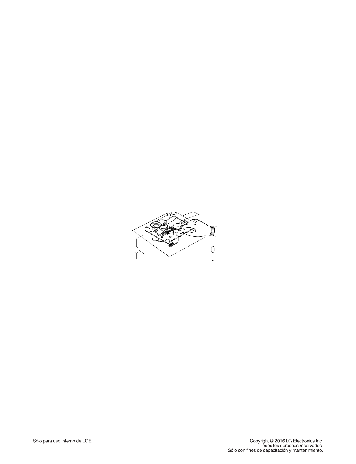
NOTAS RELACIONADAS CON LA MANIPULACIÓN DEL LECTOR
1. Notas de transporte y almacenamiento
1) El lector deberá permanecer en su bolsa conductora hasta el momento inmediatamente previo al uso.
2) El lector no debe ser expuesto a presiones externas o golpes.
Almacenamiento en bolsa conductora
2. Notas de reparación
1) El lector incluye un imán de gran tamaño, y no debe acercarse nunca a materiales magnéticos.
2) El lector debe ser manipulado correctamente y con cuidado, teniendo cuidado de evitar
presiones externas y golpes. Si así fuera, el resultado podría ser una avería operativa o daños
en la placa de circuito impreso.
3) Cada uno de los captadores ha sido ya ajustado individualmente a un alto nivel de precisión,
motivo por el que el punto de ajuste y los tornillos de instalación no deben tocarse nunca.
4) ¡El haz del láser puede dañar los ojos!
¡No mire nunca directamente al haz del láser! Igualmente, no encienda NUNCA
la alimentación de la pieza de salida láser (lente, etc.) del lector si estuviera dañado.
No mire NUNCA directamente al haz del láser, y no lo toque con
los dedos u otras partes expuestas de su cuerpo.
5) Limpieza de la superficie de la lente
Si hubiera polvo en la superficie de la lente, límpielo mediante un pulverizador (como los
empleados para limpiar las lentes de las cámaras). La lente está sujeta por un delicado soporte.
Por lo tanto, al limpiar la superficie de la lente, utilice un bastoncillo de algodón con cuidado de
Impacto por caída
Presión
Imán
Cómo sujetar el lector
Lámina
conductora
Bastoncillo de algodón
6) Nunca intente desmontar el resorte del lector ejerciendo una presión excesiva. Si la lente
estuviera extremadamente sucia, aplique alcohol isopropílico al bastoncillo de algodón. (No
utilice ningún otro limpiador líquido, ya que podría dañar la lente.) Tenga cuidado de no aplicar
demasiado alcohol en el bastoncillo, y no permita que el líquido entre en el interior del lector.
1-3
Presión
Page 5
NOTAS RELACIONADAS CON LA REPARACIÓN DE REPRODUCTORES DE CD
1. Preparación
1) Los reproductores de CD incorporan un gran número de CIs, así como un lector (diodo láser).
Estos componentes son muy sensibles y se ven fácilmente afectados por la electricidad estática. En el
caso de electricidad estática de alta tensión los componentes podrían resultar dañados, motivo por el que
deben manipularse con cuidado.
2) El lector está compuesto de numerosos componentes ópticos y otros de gran precisión.
Por lo tanto, tenga cuidado de evitar realizar labores de reparación o almacenamiento cuando la
temperatura o humedad son altas, en presencia de fuerte magnetismo o grandes cantidades de polvo.
2. Notas de reparación
1) Antes de reemplazar una pieza o componente, desconecte primero el cable de alimentación de la unidad.
2) Todo el equipamiento, instrumentos de medición y herramientas deben estar correctamente puestos a
tierra.
3) Debe cubrir su mesa de trabajo con una lámina conductora puesta a tierra. Al extraer el
lector láser de su bolsa conductora, no lo coloque sobre ésta. (El motivo es la posibilidad
de daños a causa de la electricidad estática.)
4) Para evitar la fuga de CA, la parte metálica del soldador deberá estar puesta a tierra.
5) Todos los trabajadores deberán tener conexión a tierra por medio de un brazalete especial (1 M)
6) Tenga cuidado de no permitir que el lector láser entre en contacto con la ropa, a fin de
evitar que la electricidad estática de sus prendas escape por el brazalete.
7) El haz láser del lector NUNCA debe ser dirigido hacia los ojos o la piel desnuda.
Brazalete
Resistencia
(1 M)
Resistencia
(1 M)
Lámina
conductora
1-4
Page 6
MEDIDAS DE PRECAUCIÓN ESD
Dispositivos electrostáticamente sensibles (ESD)
Ciertos dispositivos semiconductores (estado sólido) pueden resultar fácilmente dañados por la electricidad
estática. Normalmente tales componentes son conocidos comúnmente como Dispositivos electrostáticamente
sensibles (ES) Ejemplos de dispositivos ESD
típicos son los circuitos integrados y algunos transistores de efecto campo y componentes de chips semiconductores. Debe utilizar las siguientes técnicas para ayudarle a reducir las incidencias de daños en los componentes
causados por la electricidad estática.
1. Inmediatamente antes de manipular cualquier componente semiconductor o montaje equipado a tal efecto,
elimine cualquier carga electroestática presente en su cuerpo tocando una puesta a tierra segura.
Opcionalmente, obtenga y vista un dispositivo de muñequera de descarga disponible en el mercado, que
deberá retirar antes de aplicar potencia a la unidad bajo prueba a fin de evitar riesgos potenciales de descarga
eléctrica.
2. Después de retirar un montaje eléctrico equipado con dispositivos ESD, coloque el montaje sobre una superfi-
cie conductora, como papel de aluminio, para evitar la acumulación de cargas electroestáticas o la exposición
del montaje.
3. Utilice únicamente un soldador con puesta a tierra para soldar o eliminar soldaduras en los dispositivos ESD.
4. Utilice únicamente un dispositivo de eliminación de soldaduras antiestático. Ciertos dispositivos de eliminación
de soldaduras, no clasificados como “antiestáticos” pueden generar cargas eléctricas suficientes como para
dañar los dispositivos ESD.
5. No utilice productos químicos que incluya freón. Estos pueden generar cargas eléctricas suficientes como
para dañar los dispositivos ESD.
6. No saque un dispositivo ESD de repuesto de su embalaje protector hasta inmediatamente antes de su
instalación. (La mayor parte de los dispositivos ESD de repuesto están embalados con cables cortocircuitados
eléctricamente entre sí mediante espuma conductora, papel de aluminio o materiales conductores similares).
7. Inmediatamente antes de retirar el material protector de los cables de un dispositivo ESD de repuesto,
ponga en contacto el material protector y el armazón o montaje decir cuitos en los que se instalará el dispositivo.
PRECAUCIÓN: ASEGÚRESE DE QUE EL CHASIS O CIRCUITO NO RECIBE ALIMENTACIÓN LÉCTRICA,
Y RESPETE TODAS LAS PRECAUCIONES DE SEGURIDAD.
8. Minimice los movimientos corporales durante el manejo de dispositivos ESD de repuesto ya desempaqueta-
dos. (De lo contrario el movimiento inofensivo de, por ejemplo, el roce de su ropa o levantar los pies de un
suelo enmoquetado, puede generar la electricidad estática suficiente para dañar un dispositivo ESD).
PRECAUCIÓN. SÍMBOLOS GRÁFICOS
EL SÍMBOLO DEL RELÁMPAGO CON FLECHAS DENTRO DE UN TRIÁNGULO EQUILÁTERO
ESTÁ PENSADO PARA ALERTAR AL PERSONAL DE SERVICIO DE LA PRESENCIA DE
“TENSIONES PELIGROSAS” NO AISLADAS, Y QUE PUEDEN TENER LA MAGNITUD
SUFICIENTE COMO PARA CONSTITUIR UN RIESGO DE DESCARGA ELÉCTRICA.
EL SIGNO DE EXCLAMACIÓN DENTRO DE UN TRIÁNGULO EQUILÁTERO ESTÁ PENSADO
PARA ALERTAR AL PERSONAL DE SERVICIO DE LA PRESENCIA DE INFORMACIÓN
IMPORTANTE DE SEGURIDAD EN LA DOCUMENTACIÓN DE SERVICIO.
1-5
Page 7

MODO TECLA OCULTA
Presione a la vez durante 5 segundos la tecla frontal y RCU a fi n de activarlo.
1. Compruebe el código de versión y opción
Tecla frontal: PARAR
Tecla RCU: REPRODUCIR/PAUSA
Puede cambiar [Versión MCU audio <-> Versión controlador CD <-> opción EEPROM] mediante SALTAR+/-.
2. Borrar EEPROM
Tecla frontal: PARAR
Tecla RCU: SALTAR- (modelo CD), 0 (modelo DVD)
1-6
Page 8

GUÍA DE DESCARGA DE PROGRAMAS
1. PROGRAMA DE AUDIO
El nombre del archivo del programa a descargar debe ser MICOM_OM5560_YYMMDDX.HEX
Si el programa de seguridad (Water Wall) está activado en la PC, debe guardar el archivo en el dispositivo de
almacenamiento USB y desactivar el software de seguridad; A continuación, descargue el archivo al aparato.
La descarga del archivo procede en la misma forma para la función USB1 y USB2.
Precaución:
Durante la descarga del archivo, no desconecte el dispositivo USB, no cambie a otra función y no
apague el aparato. El dispositivo USB debe desconectarse cuando haya finalizado el proceso de
descarga.
EN LA PANTALLA VFD
NO USB
Conectar un dispositivo USB en función USB.
SEARCH
MICOM UP
FINISH
1) Formato (Rápido) de la memoria USB.
2) Copia el archivo de firmware a la memoria USB.
AUTO POWER OFF
1-7
Page 9
2. PROGRAMA DE CD
El nombre del archivo del programa a descargar debe ser HG690_OM5560_YYMMDDX.bin
Si el programa de seguridad (Water Wall) está activado en la PC, debe guardar el archivo en el dispositivo de
almacenamiento USB y desactivar el software de seguridad; A continuación, descargue el archivo al aparato.
La descarga del archivo procede en la misma forma para la función USB1 y USB2.
Precaución:
Durante la descarga del archivo, no desconecte el dispositivo USB, no cambie a otra función y no
apague el aparato. El dispositivo USB debe desconectarse cuando haya finalizado el proceso de
descarga.
EN LA PANTALLA VFD
NO USB
Conectar un dispositivo USB en función USB.
SEARCH
FIRMWARE
FINISH
1) Formato (Rápido) de la memoria USB.
2) Copia el archivo de firmware a la memoria USB.
AUTO POWER OFF
1-8
Page 10
3. PROGRAMA DE EQ
El nombre del archivo del programa a descargar debe ser EQ_PRG.BIN
Si el programa de seguridad (Water Wall) está activado en la PC, debe guardar el archivo en el dispositivo de
almacenamiento USB y desactivar el software de seguridad; A continuación, descargue el archivo al aparato.
La descarga del archivo procede en la misma forma para la función USB1 y USB2.
Precaución:
Durante la descarga del archivo, no desconecte el dispositivo USB, no cambie a otra función y no
apague el aparato. El dispositivo USB debe desconectarse cuando haya finalizado el proceso de
descarga.
EN LA PANTALLA VFD
NO USB
Conectar un dispositivo USB en función USB.
SEARCH
EQ UP
FINISH
1) Formato (Rápido) de la memoria USB.
2) Copia el archivo de firmware a la memoria USB.
AUTO POWER OFF
1-9
Page 11

ESPECIFICACIONES
GENERAL
Requerimientos de energía Consulte la etiqueta principal de la unidad
Consumo de Energía Consulte la etiqueta principal de la unidad
Red en espera: 0,5 W (Si todos los puertos de red están activos.)
Dimensiones (An x Alt x P) Aprox. 330 mm x 715 mm x 302 mm
Peso neto Aprox. 13 kg
Temperatura de Operación 5 °C a 35 °C (41 °F a 95 °F)
Humedad de Operación 60 %
Suministro de energía del puerto 5 V 500 mA
ENTRADAS
Entrada de audio analógica (AUX IN)
Salida de audio analógica (AUX OUT)
Entrada portátil (PORT. IN) 1,4 Vrms (toma estéreo de 3,5 mm) x 1
Micrófono (MIC 1/2) Sensibilidad 20 mV (1 kHz), 2 tomas de 6,3 mm
SINTONIZADOR
Rango de sintonización FM 87,5 a 108,0 MHz u 87,50 a 108,00 MHz
Rango de sintonización AM 522 a 1,620 kHz, 520 a 1,710 kHz u 522 a 1,710 kHz
SISTEMA
Respuesta de frecuencia Response 40 a 20 000 Hz
Relación señal-ruido Más de 75 dB
Rango dinámico Más de 80 dB
Suministro de energía del puerto (USB) 5 V 500 mA
2,0 V raíz cuadrático medio (1 kHz 0 dB), 600 Ω conector RCA (L, R)
2,0 V raíz cuadrático medio (1 kHz 0 dB), 600 Ω conector RCA (L, R)
AMPLIFICADOR (potencia de salida valor cuadrático medio total)
Salida total RMS 500 W
ALTA 160 W × 2 (4Ω a 1KHz, 10% THD)
BAJA 180 W × 1 (4Ω a 200Hz, 10% THD)
El diseño y especificaciones están sujetos a cambios sin previo aviso.
1-10
Page 12

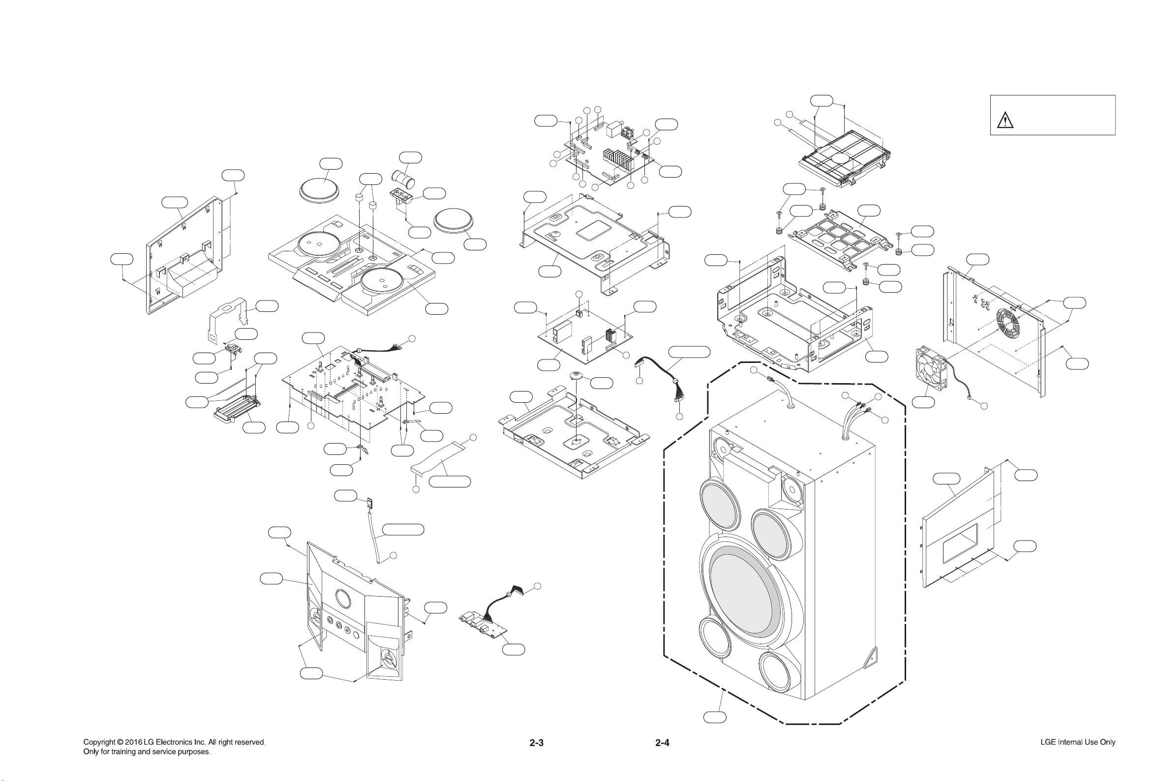
SECCIÓN 2
CARCASA Y ARMAZÓN PRINCIPAL
ÍNDICE
INSTRUCCIONES DE DESEMSAMBLE ........................................................................................................... 2-2
VISTAS AMPLIADAS ........................................................................................................................................ 2-3
1. SECCIÓN DEL GABINETE Y LA ESTRUCTURA PRINCIPAL ................................................................ 2-3
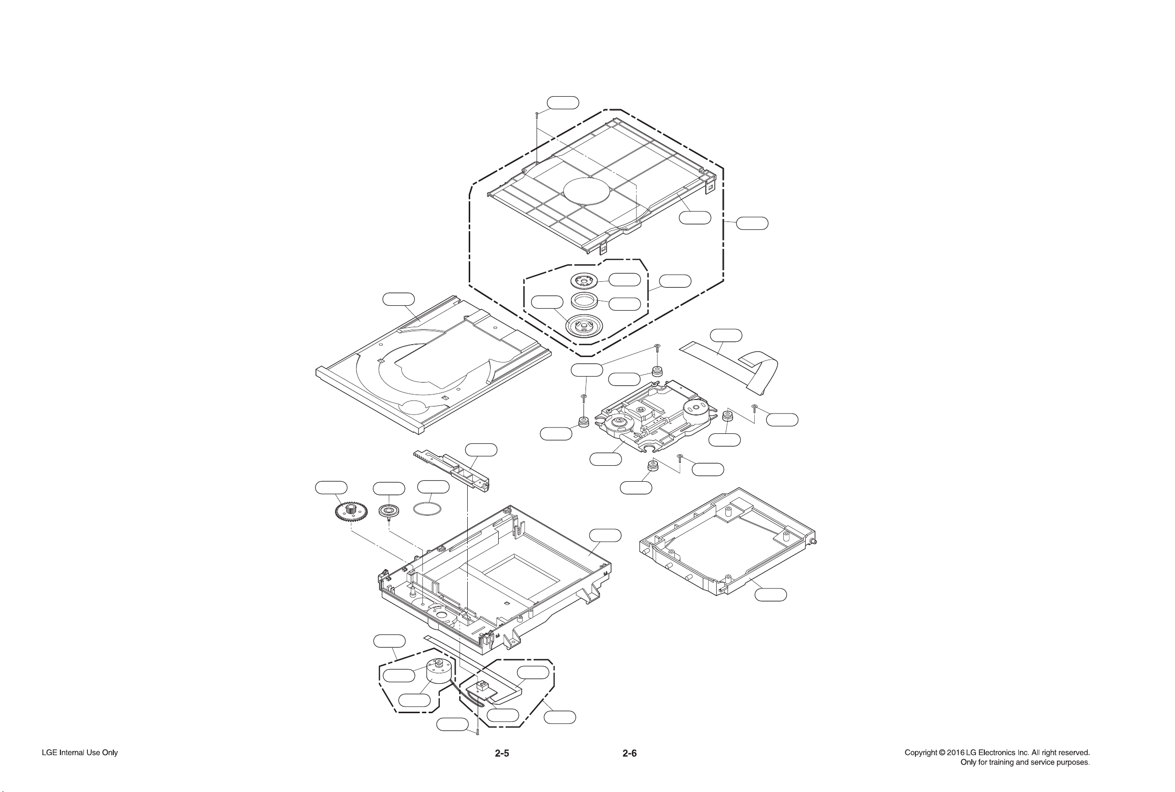
2. SECCIÓN DEL MECANISMO DE LA UNIDAD (DM19AC) ...................................................................... 2-5
3. SECCIÓN DE ACCESORIOS DE EMBALAJE ......................................................................................... 2-7
2-1
Page 13
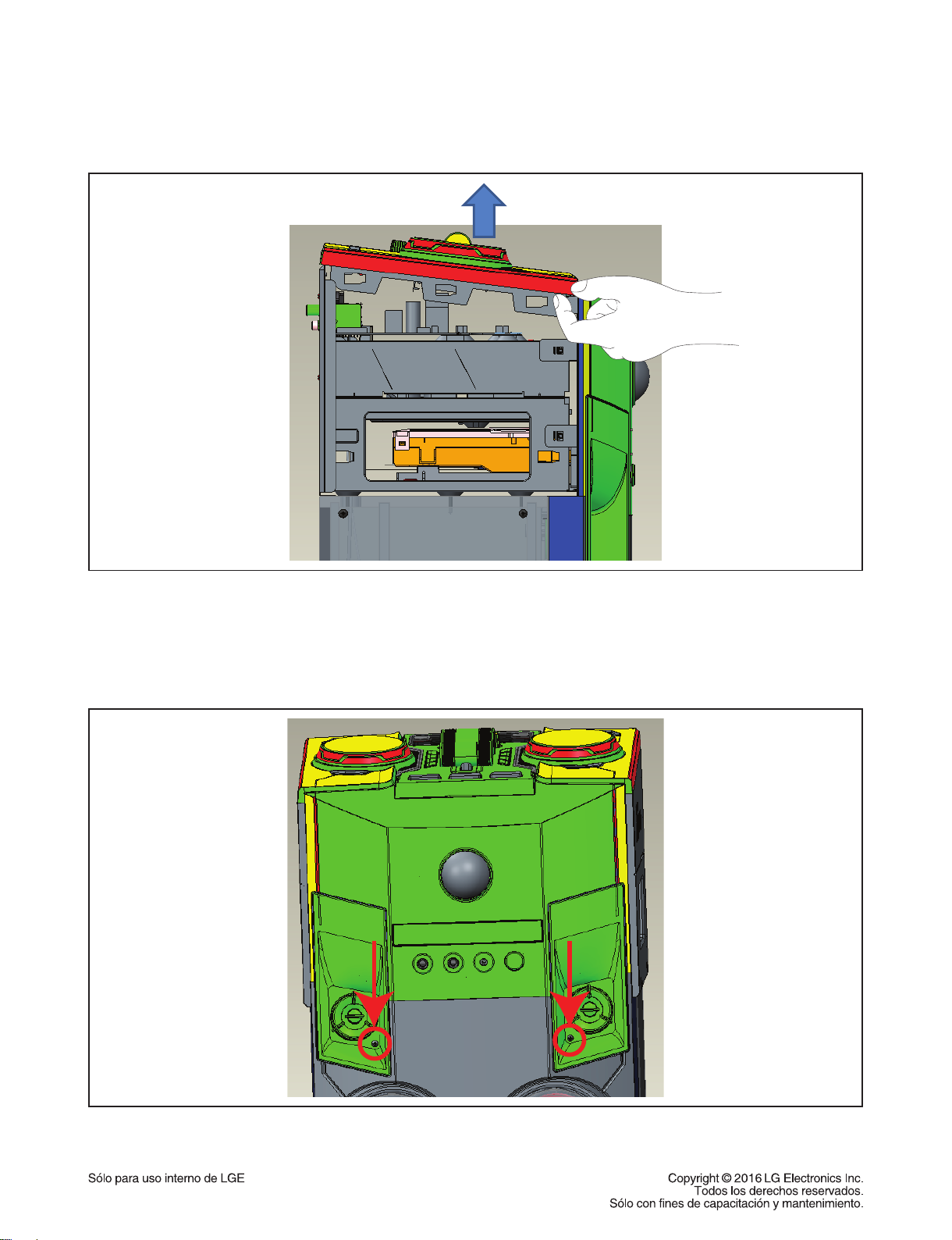
INSTRUCCIONES DE DESEMSAMBLE
1) Para desmontar la parte superior no gire y desmonte tirando hacia arriba.
Figura 1
2) Para desmontar el panel frontal, suelte los dos tornillos y proceda.
Figura 2
2-2
Page 14
RMC
TOP
E
D
H
P
J
A
C
O
I
K
L
G
K
L
B
E
D
J
I
F
G
N
N
P
H
C
A
B
O
260L
476
475
251
255
254
464
252
464
253
256
258
259
464
475
256
A50
475
270
475
A51
A41
475
475
475
475
263
475
475
275
264
476
475
260R
265
476
476
267
521
475
475
521
521
262
475
269
266
266
266
475
475
270
257
CABLE4
CABLE1
CABLE3
A44
A43
464
A60
464
464
EXPLODED VIEWS
1. CABINET AND MAIN FRAME SECTION
NOTES) THE EXCLAMATION POINT WITHIN AN
EQUILATERAL TRIANGLE IS INTENDED
TO ALERT THE SERVICE PERSONNEL
TO THE PRESENCE OF IMPORTANT
SAFETY INFORMATION IN SERVICE
LITERATURE.
MAIN
A46
SMPS
A47
Page 15
1439
A001
1002
1005
1001
1003
1004
1026
1043
A005
1016
1013
1015
1020
1439
1018
1019
1012
A006
1045
1049
1437
1437
1024
1024
1024
1024
1437
1011
1030
2. MECHANISM DECK SECTION (DM19AC)
Page 16
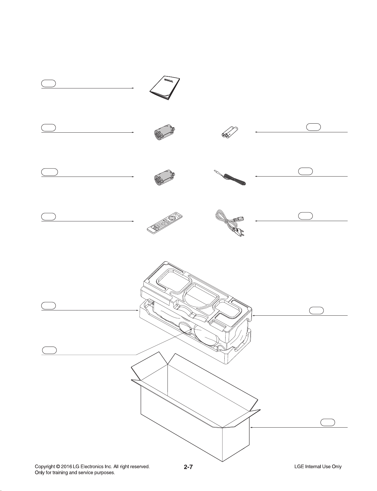
3.3. PACKING ACCESSORY SECT
801 Owner’s manual
826 Filter, Ferrite core
826A Filter, Ferrite core
900 Remote control
803 Packing
808 Batteries
825 FM antenna
300 Power Cord
803 Packing
804 Bag
802 Box
Page 17
2-8
Page 18

SECTION 3 ELECTRICAL
ONE POINT REPAIR GUIDE ............................................................................................................................ 3-2
CONTENTS
1. NO POWER ............................................................................................................................................ 3-2
2. NO BOOTING WHEN POWER ON THE SET........................................................................................ 3-3
3. VFD IS NOT DISPLAYED WHEN POWER ON THE SET ..................................................................... 3-4
4. NO BOOTING (IN CD/USB FUNCTION) ................................................................................................ 3-5
5. NO OPERATION OF MD ........................................................................................................................ 3-9
6. NO SOUND ........................................................................................................................................... 3-14
ELECTRICAL TROUBLESHOOTING GUIDE ................................................................................................. 3-22
1. POWER (SMPS) ................................................................................................................................... 3-22
2. MCS PART CHECK .............................................................................................................................. 3-25
3. FLD DISPLAY CHECK ......................................................................................................................... 3-26
4. PWM MODULATION CHECK ............................................................................................................... 3-27
5. POWER AMP PART CHECK ............................................................................................................... 3-28
6. TUNER / AUX FUNCTION CHECK ...................................................................................................... 3-29
7. TUNER FUNCTION CHECK................................................................................................................. 3-30
8. CD FUNCTION CHECK ........................................................................................................................ 3-31
9. DOUBLE USB FUNCTION ................................................................................................................... 3-32
WAVEFORMS OF MAJOR CHECK POINT .................................................................................................... 3-33
1. DSP (IC501) .......................................................................................................................................... 3-33
2. SDRAM (IC502) .................................................................................................................................... 3-34
3. SERVO (IC401) ..................................................................................................................................... 3-35
4. MOTOR DRIVER (IC400) ..................................................................................................................... 3-36
5. ADC (IC201) .......................................................................................................................................... 3-37
6. USB (CN502) ........................................................................................................................................ 3-37
7. BLUETOOTH (CN504) .......................................................................................................................... 3-38
WIRING DIAGRAM .......................................................................................................................................... 3-39
BLOCK DIAGRAMS ........................................................................................................................................ 3-41
1. SYSTEM BLOCK DIAGRAM ................................................................................................................ 3-41
2. POWER BLOCK DIAGRAM ................................................................................................................. 3-43
3. AUDIO PATH BLOCK DIAGRAM ......................................................................................................... 3-45
CIRCUIT DIAGRAMS ...................................................................................................................................... 3-47
1. SMPS CIRCUIT DIAGRAM .................................................................................................................. 3-47
2. MAIN - CD DSP CIRCUIT DIAGRAM ................................................................................................... 3-49
3. MAIN - SUB MICOM CIRCUIT DIAGRAM ...........................................................................................3-51
4. MAIN - POWER PART CIRCUIT DIAGRAM ........................................................................................ 3-53
5. MAIN - ADC/ DAC/ PWM CIRCUIT DIAGRAM .................................................................................... 3-55
6. MAIN - RF SERVO CIRCUIT DIAGRAM .............................................................................................. 3-57
7. MAIN - PWM/ AMP CIRCUIT DIAGRAM .............................................................................................. 3-59
8. MAIN - FAN & LED LIGHTING CIRCUIT DIAGRAM ........................................................................... 3-61
9. TOP FRONT CIRCUIT DIAGRAM ........................................................................................................ 3-63
10. JACK/ RMC CIRCUIT DIAGRAM ......................................................................................................... 3-65
CIRCUIT VOLTAGE CHART ........................................................................................................................... 3-67
1. IC INPUT VOLTAGE ............................................................................................................................. 3-67
2. CAPACITOR VOLTAGE ....................................................................................................................... 3-68
3. CONNECTOR VOLTAGE ..................................................................................................................... 3-69
PRINTED CIRCUIT BOARD DIAGRAMS ....................................................................................................... 3-73
1. SMPS P.C.BOARD ............................................................................................................................... 3-73
2. MAIN P.C.BOARD ................................................................................................................................ 3-75
3. TOP FRONT P.C.BOARD .................................................................................................................... 3-79
4. JACK/ RMC P.C.BOARD ...................................................................................................................... 3-83
3-1
Page 19
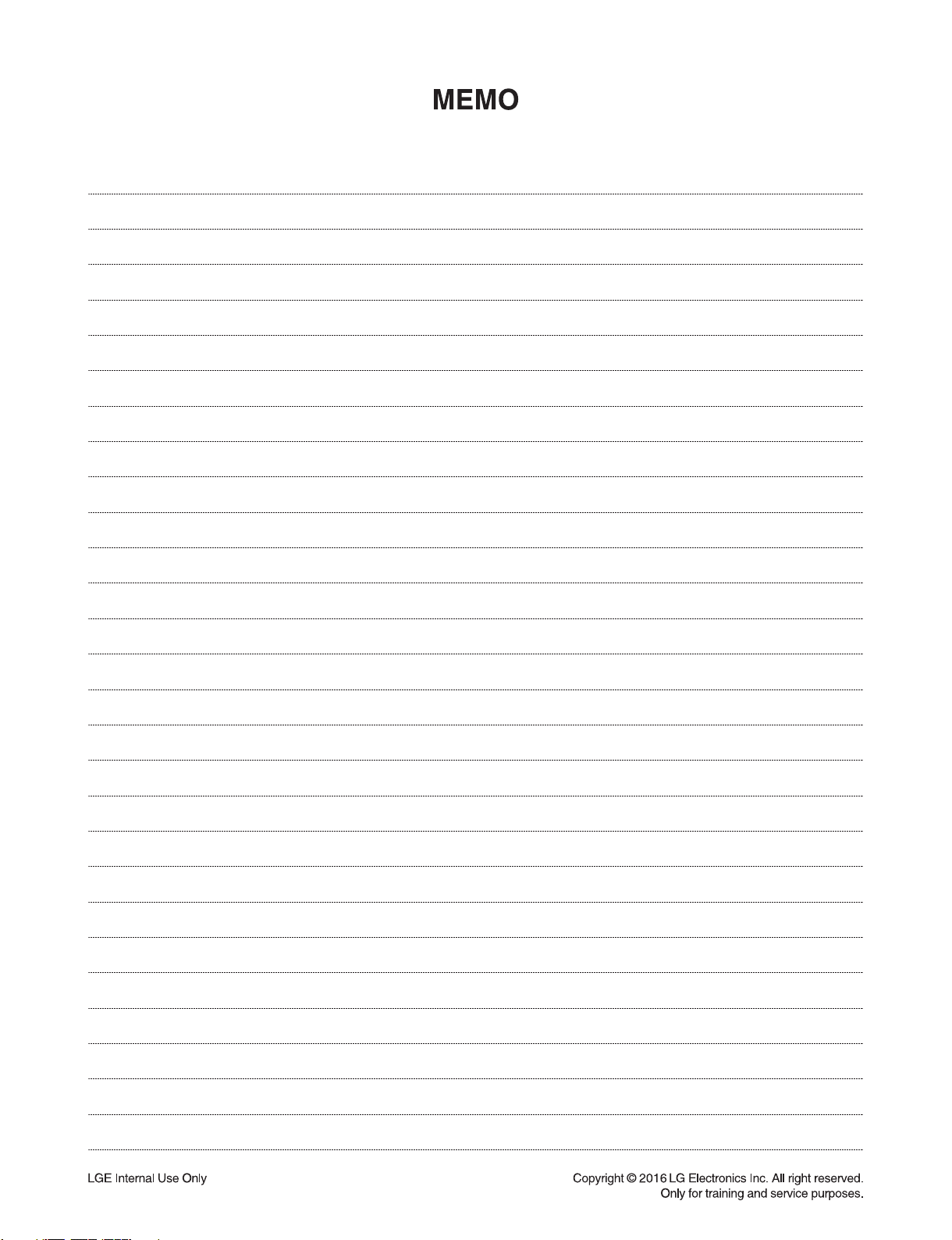
ONE POINT REPAIR GUIDE
1. NO POWER
If the unit doesn’t work by no power problem, repair the set according to the following guide.
1-1. FUSE/ THERMISTOR/ BRIDGE DIODE
1-1-1. Solution
Please check and replace F901, TH901 or TH903, BD901 on SMPS board.
1-1-2. How to troubleshoot (Countermeasure)
1) Check if the fuse F901 is open or short-circuit.
2) Check if the NTC thermistor TH900 or TH903 is normal or open.
3) Check if the bridge diode BD901 is short-circuit by over current with a digital multi-meter.
1-1-3. Service hint (Any picture/ Remark)
< F901 >
If F901 is not short-circuit,
replace it with a same
specifi cations one.
<TH901 or TH903 >
If TH901 or TH903 is open,
replace it with a new one.
3-2
< BD901 >
If BD901 is short-circuit,
replace it with a new one.
Page 20
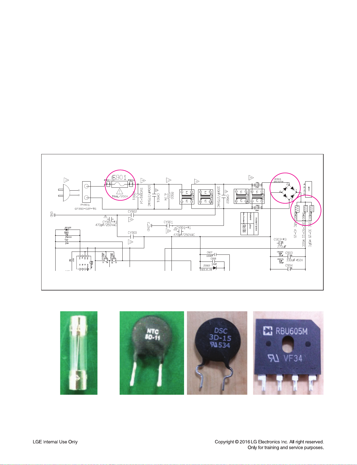
ONE POINT REPAIR GUIDE
NO POWER
If the unit doesn’t work by no PVDD problem, repair the set according to the following guide.
1-2. FUSE/ FET
1-2-1. Solution
Please check and replace F901, Q901 on SMPS board.
1-2-2. How to troubleshoot (Countermeasure)
1) Check if the fuse F901 is open or short-circuit.
2) Check the anode-cathod voltage of D951 with a digital multi-meter, it is normally 0.2 ~ 0.3 V.
If it doesn’t have any voltage, it’s destroyed. Replace it with a new one.
1-2-3. Service hint (Any picture/ Remark)
< SMPS circuit >
3-3
Page 21
ONE POINT REPAIR GUIDE
X500
(24 MHz)
X501
(32.768 kHz)
KEY1
(R518)
PWR_CTRL
R559
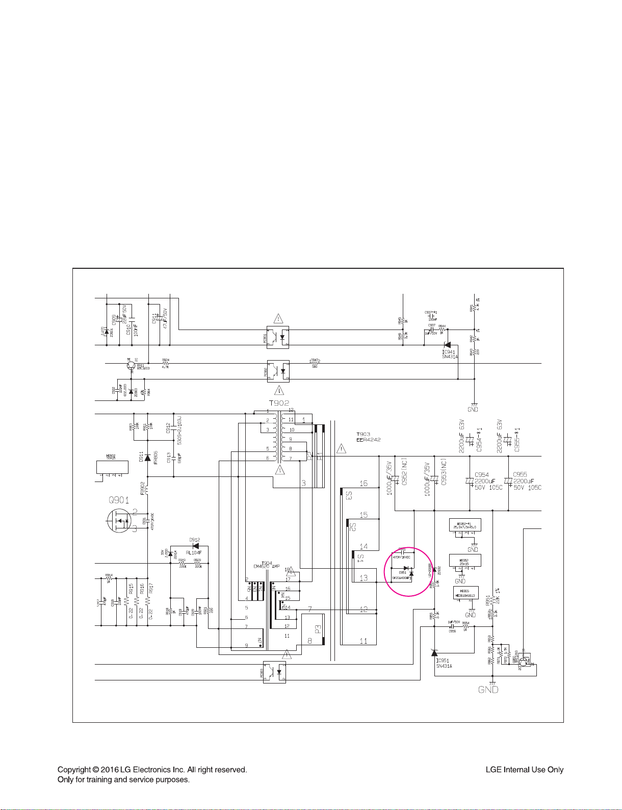
2. NO BOOTING WHEN POWER ON THE SET
The set doesn’t work when press the power button on the top board or the remote control.
2-1. IC501
2-1-1. Solution
Replace IC501 on MAIN board.
2-1-2. How to troubleshoot (Countermeasure)
1) Check the +12 VA (CN202) and 3.3VA (IC503) in standby mode.
If there is no 12 VA, check the SMPS and if doesn’t appear 3.3 VA, check IC503.
2) Check +12 VA, +5.1 VA, 3.3 VA, DVCC_5V and DVCC_3.3V when power on the set.
If the set doesn’t work regardless of what the KEY1 changes high to low while pressing the power button.
-
X500 and X501 work normally but, if you can not power on the set, replace the IC501 with a new one
on the main board.
2-1-3. Service hint (Any picture/ Remark)
X501
(32.768 kHz)
KEY1
(R518)
X500
(24 MHz)
< MAIN board top view >
PWR_CTRL
R559
< MAIN board bottom view >
3-4
Page 22
ONE POINT REPAIR GUIDE
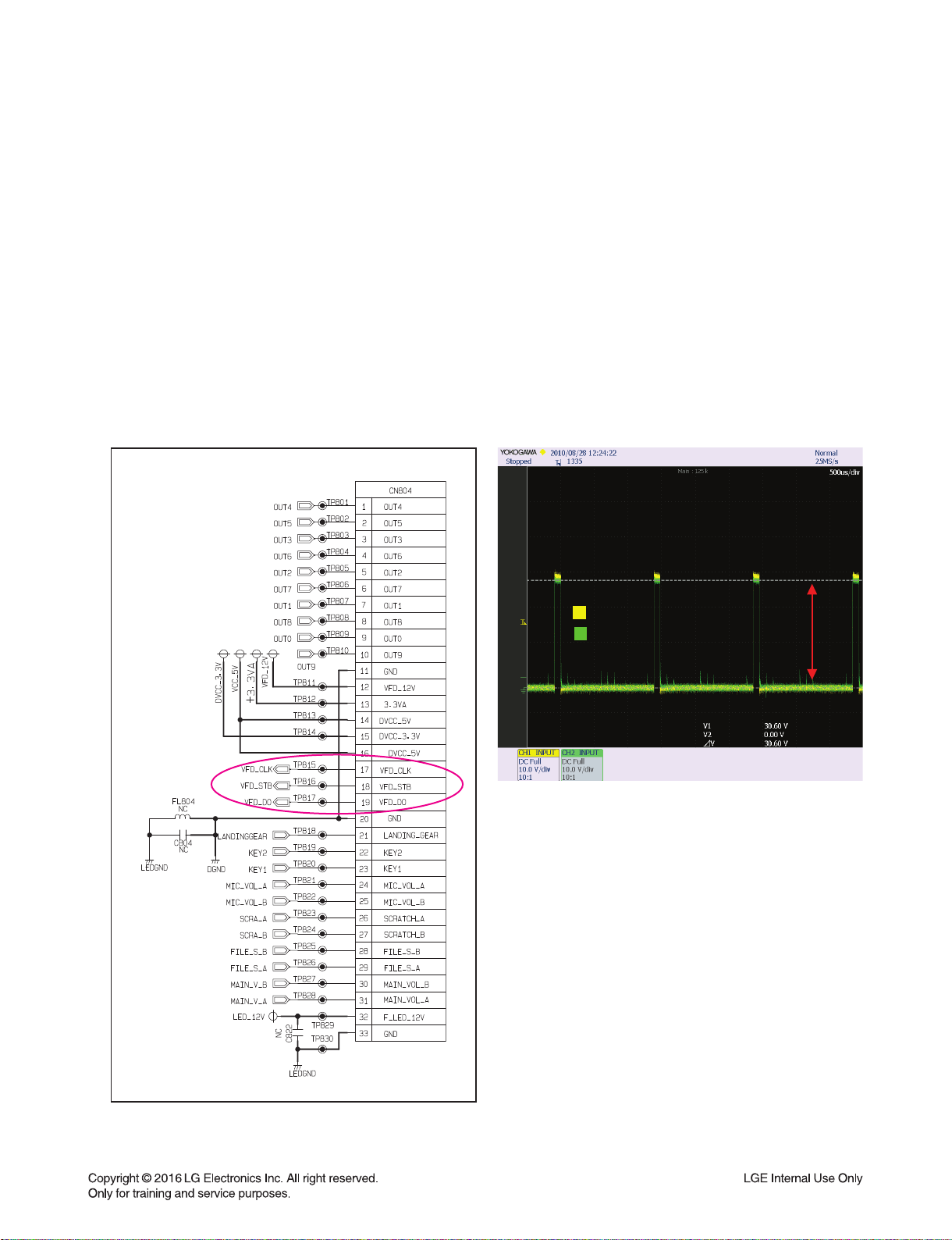
3. VFD IS NOT DISPLAYED WHEN POWER ON THE SET
When power on the set, any icons or characters on VFD are not displayed.
3-1. VFD (VFD301)
3-1-1. Solution
Please check and replace VFD301 on TOP FRONT board.
3-1-2. How to troubleshoot (Countermeasure)
1) Check if VFD_12V, DVCC_3.3V and VCC_5V are output from SMPS to VFD via the main board.
2) Check if the IC501 outputs VFD_CLK, VFD_STB, and VFD_DAT to the top board.
3) Check if the VFD grid current amplifier circuit on the top board.
Check the drive signal to the transistor’s(Q801,2) base.
If the control signals from VFD (DGND, VDD) isn’t output, replace VFD with a new one.
3-1-3. Service hint (Any picture/ Remark)
R812(TP 841)
Q801 Emitte r
< Waveform of the grid current driver>
about
30 Vp-p
< TOP FRONT circuit >
3-5
Page 23
ONE POINT REPAIR GUIDE
IC505
IC202
IC205
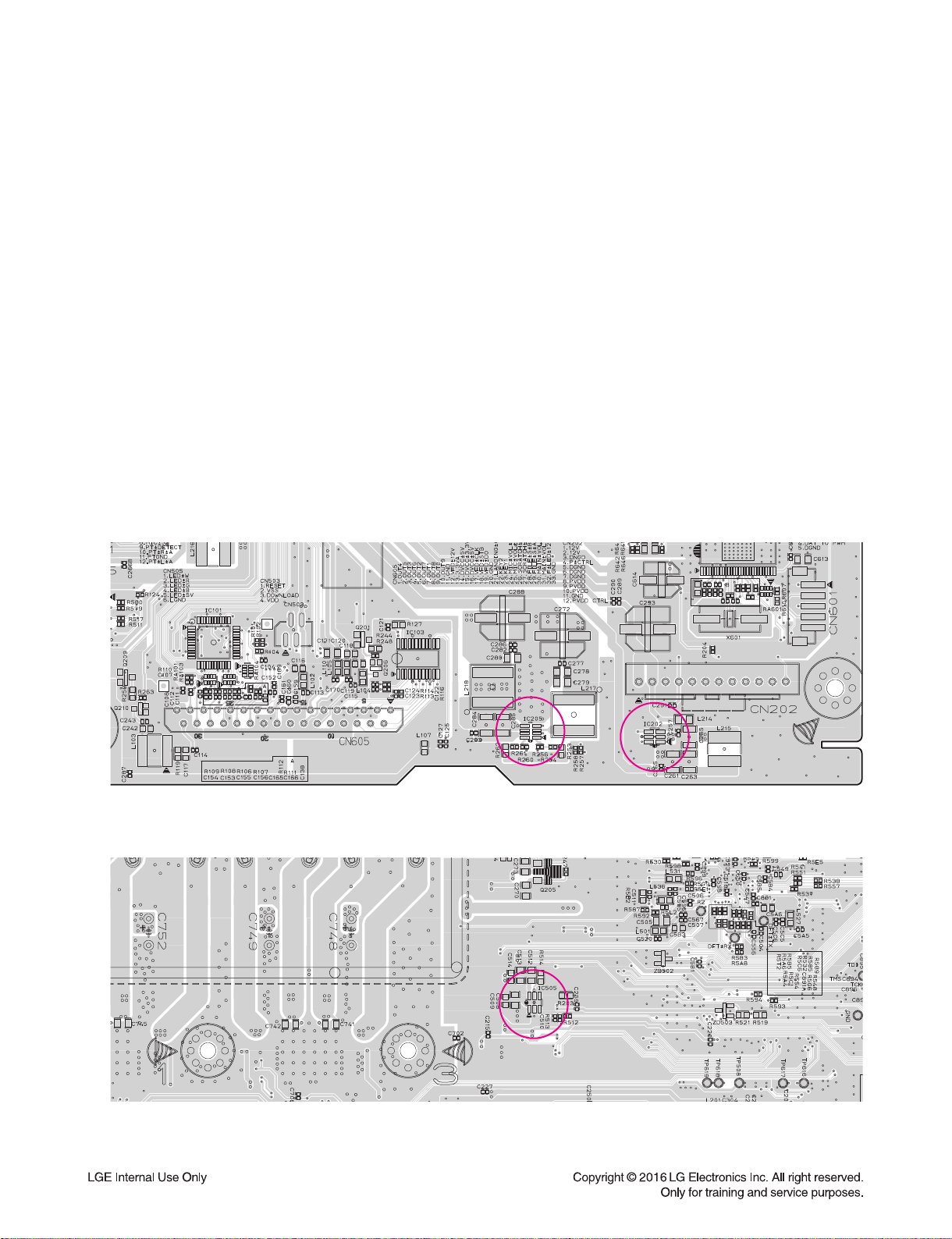
4. NO BOOTING (IN CD/USB FUNCTION)
After you turn on power key and displayed message in the following order (HELLO VOL XX
CD or USB) on VFD, it will not display other message on VFD, and it will not boot-up normally.
4-1. NO DVCC_3.3V, 1.2 VA
4-1-1. Solution
Please check and replace IC202, IC205 on MAIN board.
4-1-2. How to troubleshoot (Countermeasure)
1) Check Voltage of IC202 pin3 on MAIN board.
If IC202 pin3 (about 5.1 V) & pin1 Input 12 VA doesn’t come out, check +12 VA from SMPS board.
2) If IC202 pin3 (about 5.1 V) is normal, check voltage of IC205 pin3 (about 1.2 VA), pin6 (about 3.3 VA).
If IC205 pin3 (about 1.2 VA), pin6 (about 3.3 VA) doesn’t come out, check R253, R254, R256 and R260, R261, R262.
If there’s no defective component then replace IC205.
3) PWR_CTRL is high, check R512 and if there’s no defective component then replace IC505.
PWR_CTRL (IC505 pin3) is high (about 3.2 V)
If PWR_CTRL isn’t high, check pin D11 of IC501 & R512, R513
4) If PWR_CTRL is high, check R559 and if there’s no defective component then replace IC505.
4-1-3. Service hint (Any picture/ Remark)
IC205
< MAIN board top view >
IC505
< MAIN board bottom view >
IC202
3-6
Page 24

ONE POINT REPAIR GUIDE
XI
XO
IC501
X500
NO BOOTING (IN CD/USB FUNCTION)
After you turn on power key and displayed message in the following order (HELLO VOL XX
CD or USB) on VFD, it will not display other message on VFD, and it will not boot-up normally.
4-2. CRYSTAL (X500)
4-2-1. Solution
Replace X500 on MAIN board.
4-2-2. How to troubleshoot (Countermeasure)
1) If 3.3 VA & 1.2 VA is normal, check reset ‘High’ of IC501 pin T12 on MAIN board.
If MAIN_RESET isn’t high, check MICOM (IC101) pin40.
2) If MAIN_RESET is high, check the soldering status of 24 MHz crystal (X500).
3) If the crystal (X500) doesn’t oscillate, check R508, C502, C503 around crystal (X500).
If there’s no defective component, then replace X500.
4-2-3. Service hint (Any picture/ Remark)
IC501
X500
< MAIN board top view >
X
X500
< Signal waveform >
3-7
Page 25

ONE POINT REPAIR GUIDE
VCC
CLK
DO
CS#
IC503
NO BOOTING (IN CD/USB FUNCTION)
After you turn on power key and displayed message in the following order (HELLO VOL XX
CD or USB) on VFD, it will not display other message on VFD, and it will not boot-up normally.
4-3. SERIAL FLASH (IC503)
4-3-1. Solution
Please check and replace IC503 on MAIN board.
4-3-2. How to troubleshoot (Countermeasure)
1) If the crystal (X500) does oscillate, check serial flash (IC503) on MAIN board.
Check pin8 (VCC), pin6 (CLK), pin1 (CS), pin2 (DO), pin5 (DI) of below waveform.
2) If pin1, 2, 5, 6 doesn’t come out, check registers (R563, R564, R534, R535, R536, R5E4) of IC503.
If registers of IC503 is OK, then replace IC503. (it need to download program.)
3) After change IC503, if It is still not below waveform, check IC501 (DSP IC).
4-3-3. Service hint (Any picture/ Remark)
IC503
< MAIN board bottom view >
< Signal waveform >
3-8
Page 26

ONE POINT REPAIR GUIDE
SP+: pin18
SP-: pin19
IC400
5. NO OPERATION OF MD
When no sound output in the CD function, you can not listen to music reading data from a CD
disc if the servo motors in MD don’t work. This step is for checking the SPINDLE MOTOR among
them.
5-1. SPINDLE MOTOR
5-1-1. Solution
Replace IC400 on MAIN board.
5-1-2. How to troubleshoot (Countermeasure)
1) Check the SPDO signal from pin16 of IC401.
If no signal, check DVCC_3.3V and DV 3.3V (RF) and X400.
2) Check the SPIN+ & SPIN- from IC400 to CN401 for driving SPINDLE motor. It is about 3.6 Vp-p.
If no signal, check M_5 V for IC400.
3) Check if the FFC cable is solidly connected between CN401 and MD.
4) Check the MD.
If the spindle motor is sort-circuit or has any trouble, it can not rotate CD discs.
Please check the function after changing another MD.
5-1-3. Service hint (Any picture/ Remark)
< Waveform of SP- & SP+
for driving SPINDLE motor >
SP+: pin18
SP-: pin19
< MAIN board top view >
IC400
3-9
Page 27

ONE POINT REPAIR GUIDE
SLED+: pin11
SLED-: pin12
IC400
NO OPERATION OF MD
When no sound output in the CD function, you can not listen to music reading data from a CD
disc if the servo motors in MD don’t work. This step is for checking the SLED MOTOR among
them.
5-2. SLED MOTOR
5-2-1. Solution
Replace IC400 on MAIN board.
5-2-2. How to troubleshoot (Countermeasure)
1) Check the SLDO signal from pin15 of IC401.
If no signal, check DVCC_3.3V and DV 3.3V(RF) and X400.
2) Check the SPED+ & SLED- from IC400 to CN401 for driving SPINDLE motor. It is about 2.9 Vp-p.
If no signal, check M_5 V for IC400.
3) Check if the FFC cable is solidly connected between CN401 and MD.
4) Check the MD.
If the spindle motor is sort-circuit or has any trouble, it can not rotate CD discs.
Please check the function after changing another MD.
5-2-3. Service hint (Any picture/ Remark)
SP+
SP-
< Waveform of SLED- & SLED+
for driving SLED motor >
SLED+: pin11
SLED-: pin12
< MAIN board top view >
IC400
3-10
Page 28

ONE POINT REPAIR GUIDE
MOT_CLOSE: pin6
MOT_OPEN: pin7
LOAD+: pin9
LOAD-: pin10
IC400
NO OPERATION OF MD
When no sound output in the CD function, you can not listen to music reading data from a CD
disc if the servo motors in MD don’t work. This step is for checking the TRAY OPEN / CLOSE
MOTOR among them.
5-3. TRAY OPEN/ CLOSE MOTOR
5-3-1. Solution
Replace IC400 on MAIN board.
5-3-2. How to troubleshoot (Countermeasure)
1) Check MOT_OPEN & MOT_CLOSE signals from pin P5, L4 of IC501 to IC400.
If no signal, check M_5V to IC400.
2) Check LOAD± from IC400 to CN401 for driving the tray open / close motor. It is about 3.85 Vp-p.
If no signal, check M_5V to IC400. If it has any trouble, replace it with a new one.
3) Check if the FFC cable is solidly connected between CN401 and MD.
4) Check the MD.
If the tray motor is sort-circuit or has any trouble, it can not open or close the tray.
Please check the function after changing another MD.
5-3-3. Service hint (Any picture/ Remark)
LO-
LO+(RED)
MOT_OP EN
MOT_ CL OSE
< Waveform
for driving tray open/ close motor >
MOT_CLOSE: pin6
MOT_OPEN: pin7
LOAD+: pin9
LOAD-: pin10
< MAIN board top view >
IC400
3-11
Page 29

ONE POINT REPAIR GUIDE
TR+: pin16
TR-: pin15
IC400
NO OPERATION OF MD
When no sound output in the CD function, you can not listen to music reading data from a CD
disc if the pickup module in MD doesn’t work. This step is for checking the LASER TRACKING
ACTUATOR.
5-4. LASER TRACKING ACTUATOR
5-4-1. Solution
Replace IC400 on MAIN board.
5-4-2. How to troubleshoot (Countermeasure)
The tracking actuator makes the laser beam be positioned in the center of a track on CD disc.
1) Check the TRD signal from pin14 of IC401.
If no signal, check DVCC_3.3V & DV_3.3V (RF) and X400.
2) Check TR- & TR+ from IC400 to CN400 for driving the tracking actuator.
If no signal, check M_5V for IC400.
3) Check if the FFC cable is solidly connected between CN400 and MD.
4) Check the MD.
If the pickup module has any trouble, it can not move the laser beam on the left or right side.
Please check the function after changing another MD.
5-4-3. Service hint (Any picture/ Remark)
< Waveform of TR±
for driving tracking actuator >
TR+: pin16
TR-: pin15
< MAIN board top view >
IC400
3-12
Page 30

ONE POINT REPAIR GUIDE
F+: pin14
F-: pin13
IC400
NO OPERATION OF MD
When no sound output in the CD function, you can not listen to music reading data from a CD
disc if the pickup module in MD doesn’t work. This step is for checking the LASER FOCUSING
ACTUATOR.
5-5. LASER FOCUSING ACTUATOR
5-5-1. Solution
Replace IC400 on MAIN board.
5-5-2. How to troubleshoot (Countermeasure)
The focusing actuator makes the laser beam keep a regular interval with the surface of a CD disc.
1) Check the FDO signal from pin13 of IC401.
If no signal, check DVCC_3.3 & DV_3.3V(RF) and X400.
2) Check F- & F+ from IC400 to CN400 for driving the focusing actuator.
If no signal, check M_5V for IC400.
3) Check if the FFC cable is solidly connected between CN400 and MD.
4) Check the MD.
If the pickup module has any trouble, it can not move the laser beam on the top or bottom side.
Please check the function after changing another MD.
5-5-3. Service hint (Any picture/ Remark)
< Waveform of F±
for driving focusing actuator >
F+: pin14
F-: pin13
< MAIN board top view >
IC400
3-13
Page 31

ONE POINT REPAIR GUIDE
IC701
L703
L702
L701
L704
IC702
IC601
6. NO SOUND
There is no sound output by DIGITAL AUDIO AMP DAMAGE, repair the set according to the
following guide.
6-1. DIGITAL AUDIO AMP DAMAGE
6-1-1. Solution
Replace IC701, IC702 on MAIN board.
6-1-2. How to troubleshoot (Countermeasure)
1) Check PWM_FL±, PWM_FR± & PWM_SW± signals from IC601 to IC701 & 702 each input function.
If no signal, check if I2S audio signals are entered to IC601.
2) Check PVDD.
If PVDD is abnormal, check the SMPS.
3) Check AMP_12V for driving the gate of AMP IC.
a. All the powers are normal, but if AMP_12V is low, there is possible for AMP IC to be damaged.
b. Remove L701, L702, L703 and L704 one by one.
When removed a inductance, if AMP_12V is recovered, the IC connected to it was damaged.
c. Replace the IC with a new one.
4) Check the impedance between IC701/IC702_OUT_A/OUT_B & GND.
a. If the impedance is 0 Ω, the IC must be damaged.
b. After removing the heat sink, replace it with a new one.
6-1-3. Service hint (Any picture/ Remark)
L703
IC701
L701
L704
IC702
IC601
L702
< MAIN board top view >
3-14
Page 32

ONE POINT REPAIR GUIDE
IC501
R503
NO SOUND
There is no sound output in the CD FUNCTION, repair the set according to the following guide.
6-2. CD FUNCTION
6-2-1. Solution
Replace IC501 on MAIN board.
6-2-2. How to troubleshoot (Countermeasure)
1) Check CD_BCK, CD_LRCK, & CD_DATA signals from IC501 to IC401.
If no signal, check if the RF & servo signals from MD is entered to IC401.
Refer to the “No operation of MD” guide on Item 5.
2) Check the following I2S signal flow. < I2S audio signal Interface >
- MCS_BCK : IC501_pin E1 --> IC601_pin23
- MCS_LRCK : IC501_pin D1 --> IC601_pin22 (44.1 kHz)
- MIX_DATA0_OUT : IC501_pin E2 --> IC601_pin24
- MCS_MCLK : IC501_pin D2 --> IC201_pin44
If there is any trouble, check the power for each IC.
The power is normal but, if the signal waveform to the IC is distorted or no signal,
replace it with a new one.
6-2-3. Service hint (Any picture/ Remark)
< Waveform of I2S audio interface signals >
< MAIN - CD DSP circuit >
IC501
R503
< MAIN board top view >
3-15
Page 33

ONE POINT REPAIR GUIDE
D+
D-
CN502
NO SOUND
There is no sound output in the USB Function, repair the set according to the following guide.
6-3. USB FUNCTION
6-3-1. Solution
Replace IC204 on MAIN board.
6-3-2. How to troubleshoot (Countermeasure)
1) Check +5V_USB to USB board.
If the USB LED are turned on, the voltage is okay, if so not, check USB_5V to pin5, 6 of CN803.
2) Check USB D1± or USB D2± from MAIN board to TOP board.
a. Check 2.0_D1±signals(pin U7, U8 ) or 1.1_D1± signals(pin A7, A8 ) to IC501.
b. Check USB± signals to CN502(pin1, 2, 8, 9).
If there is any trouble, check the power for IC204.
The power is normal but, if the signal waveform to the IC is distorted or no signal,
replace it with a new one.
3) Check if “Digital audio AMP block” on item 6-1 is normal.
6-3-3. Service hint (Any picture/ Remark)
D
USB D-/D+ (CN502 pin1, 2 & pin8, 9)
< Waveform of USB D± signal >
CN502
< MAIN board top view >
3-16
Page 34

ONE POINT REPAIR GUIDE
MCS_BCK: pin42
MCS_LRCK: pin43
MCS_MLCK: pin44
IC201
NO SOUND
There is no sound output in the AUX Function, repair the set according to the following guide.
6-4. AUX FUNCTION
6-4-1. Solution
Replace IC201 on MAIN board.
6-4-2. How to troubleshoot (Countermeasure)
1) Check AUX_L/R signals to IC201 (pin23, 24).
2) Check if MCS_BCK, MCS_LRCK & MCS_MCLK are entered from IC501 to IC201.
3) Check if ADC_DATA is entered from IC201 to IC501.
If no signal, check DVCC_5V & DVCC_3.3V (ADC) for IC201. If is NG, replace it a new one.
4) Check the following I2S signal flow from IC501 to IC601. (Refer to Item 6-2.)
If there is any trouble, check the power for each IC. The power is normal but, if the signal waveform
to the IC is distorted or no signal, replace it with a new one.
5) Check if the digital audio AMP block is okay. Refer to “Digital Audio AMP” guide on Item 6-1.
If AMP is damaged, replace it with a new one.
6-4-3. Service hint (Any picture/ Remark)
MCS_BCK: pin42
MCS_LRCK: pin43
MCS_MLCK: pin44
IC201
< AUX function signal fl ow >
< MAIN board bottom view >
3-17
Page 35

ONE POINT REPAIR GUIDE
TUNER_L: pin26
TUNER_R: pin27
IC201
NO SOUND
There is no sound output in the TUNER function, repair the set according to the following guide.
6-5. TUNER FUNCTION
6-5-1. Solution
Replace IC201 on MAIN board.
6-5-2. How to troubleshoot (Countermeasure)
1) Check if TUNER_LR is entered from pin1, 3 of TU500 to IC201 (pin26, 27).
If no signals, check DVCC_3.3V for tuner power.
Check if the tuner control signals (CLK, DAT, CE, RST, SLT) are entered from IC501 to TU500.
If it doesn’t work, replace TUNER with a new one.
2) Check if MCS_BCK, MCS_LRCK, & MCS_MCLK are entered from IC501 to IC201.
3) Check if ADC_DATA is entered from IC201 to IC501.
If no signal, check DVCC_5V & DVCC_3.3V (ADC) for IC201. If is NG, replace it with a new one.
4) Check the following I2S audio signal flow from IC501 to IC601. (Refer to Item 6-2.)
If there is any trouble, check the power for each IC.
The power is normal but, if the signal waveform to the IC is distorted or no signal,
replace it with a new one.
5) Check if the digital audio AMP block is okay. Refer to “Digital Audio AMP” guide on Item 6-1.
If AMP is damaged, replace it with a new one.
6-5-3. Service hint (Any picture/ Remark)
TUNER_L: pin26
TUNER_R: pin27
IC201
< TUNER function signal fl ow >
< MAIN board bottom view >
3-18
Page 36

ONE POINT REPAIR GUIDE
PT_L: pin9
PT_R: pin10
IC201
NO SOUND
There is no sound output in the PORTABLE Function, repair the set according to the following guide.
6-6. PORTABLE FUNCTION,
6-6-1. Solution
Replace IC201 on MAIN board.
6-6-2. How to troubleshoot (Countermeasure)
1) Check if PT_LR signals to IC201 (pin9, 10).
2) Check if MCS_BCK, MCS_LRCK, & MCS_MCLK are entered from IC501 to IC201.
3) Check if ADC_DATA is entered from IC201 to IC501.
If no signal, check DVCC_5V & DVCC_3.3V (ADC) for IC201. If is NG, replace it with a new one.
4) Check the following I2S audio signal flow from IC501 to IC601. (Refer to Item 6-2.)
If there is any trouble, check the power for each IC.
The power is normal but, if the signal waveform to the IC is distorted or no signal,
replace it with a new one.
5) Check if the digital audio AMP block is okay. Refer to “Digital Audio AMP” guide on Item 6-1.
If AMP is damaged, replace it with a new one.
6-6-3. Service hint (Any picture/ Remark)
IC201
PT_L: pin9
PT_R: pin10
< PORT. IN function signal fl ow >
< MAIN board bottom view >
3-19
Page 37

ONE POINT REPAIR GUIDE
IC206
ADC/ MIC_DATA: pin9
MCS_BCK: pin8
MCS_LRCK: pin7
MCS_MCLK: pin6
NO SOUND
There is no sound output in the MIC IN function, repair the set according to the following guide.
6-7. MIC IN function
6-7-1. Solution
Replace IC206 on MAIN board, ICA301 on TOP FRONT board.
6-7-2. How to troubleshoot (Countermeasure)
1) Check MIC_SI & MIC_S2 signal to pin5 & 6 of CN201.
If no signal, Check the signals to pin6 & 8 of CNA301 on the FRONT board.
Check if the signal is entered from pin 6 & 8 of CNA301 to pin 5 & 6 of CN201.
2) Check if MIC_SIG is entered from pin 6 of JK302 & JKA303 to pin2, 13 to ICA301 (PRE AMP).
3) Check if the amplified signal comes out from pin3 &12 of ICA301.
If no signal output, check DVCC_3.3V for ICA301, replace ICA301 with a new one if it has a problem.
4) Check if MCS_BCK, MCS_MLCK & MCS_LRCK is entered from IC501 to IC206.
Check if MIC_DATA_IN is entered from pin9 of IC206 to pin T1of IC501.
If no signal, check DVCC_5V & DVCC_3.3V for IC206.
If it is abnormal, change replace it a new one.
5) Check the following I2S signal flow from IC206 to IC501.
If there is any trouble, check the power for each IC.
If the signals are abnormal, replace it a new one.
6) Check if the digital audio AMP block is okay. Refer to “Digital Audio AMP” guide on item 6-1.
If AMP is damaged, replace it with a new one.
6-7-3. Service hint (Any picture/ Remark)
ADC/ MIC_DATA: pin9
MCS_BCK: pin8
MCS_LRCK: pin7
MCS_MCLK: pin6
IC206
< MAIN board bottom view >
3-20
Page 38

ONE POINT REPAIR GUIDE
NO SOUND
There is no sound output in the Bluetooth function, repair the set according to the following guide.
6-8. BLUETOOTH FUNCTION
6-8-1. Solution
Replace IC501 on the MAIN board or bluetooth module on the FRONT Panel.
6-8-2. How to troubleshoot (Countermeasure)
1) Check BT_RX, BT_TX signal to pin6, 4 of CN504.
If no signal, check the signal to pin4, 6 and pin10 (BT_3.3V) of on the Bluetooth module
and cable connection state.
If there are no signal out from module, replace new module.
2) Check if BT_RX/TX is entered from pin6, 4 of CN504 to pin L1,K1 to IC501 (DSP).
3) Check if MCS_BCK, MCS_LRCK & MIX_DATA IN is entered from IC501 to IC601.
If no signal, check +3.3 VA & +1.2 VA for IC501.
If it is abnormal, change replace it a new one.
4) Check the following I2S signal flow from IC501 to IC601.
If there is any trouble, check the power for each IC.
If the signals are abnormal, replace it a new one.
5) Check if the digital audio AMP block is okay. Refer to “Digital Audio AMP” guide on item 6-1.
If AMP is damaged, replace it with a new one.
6-8-3. Service hint (Any picture/ Remark)
B/T Module
BT_RX,
BT_TX
IC501
MLC3730
IC601
TPS5548DGG
MCS_BCK
MCS_LRCK
MIX_DATA0_OUT
PWM
TPS5631B
AMP
< Bluetooth function signal fl ow >
< MAIN board bottom view >
3-21
Page 39

ELECTRICAL TROUBLESHOOTING GUIDE
1. POWER (SMPS)
No 12 VA
YES
F901 normal?
YES
BD901 normal?
YES
TH901(TH903) normal?
YES
Is Vcc
(10 V ~ 18 V) supplied to
IC901 pin7?
YES
D933 normal?
NO
Replace F901 (Use the same fuse).
NO
Replace BD901.
NO
Replace TH901.
NO
D902 normal?
NO
Check or replace D902.
NO
Replace D933.
YES
Is there
about 2.5 V at
IC941 pin1?
YES
D951 normal?
YES
ZD932 normal?
YES
Power line of main PCB is short.
NO
Replace IC941.
NO
Replace D951.
NO
Replace ZD932.
3-22
Page 40

ELECTRICAL TROUBLESHOOTING GUIDE
No PVDD
YES
F901 normal?
YES
BD901 normal? Replace BD901.
YES
TH901(TH903) normal?
YES
NO
NO
NO
Replace F901 (Use the same fuse).
Replace TH901.
(10 V ~ 18 V) supplied to
Is Vcc
IC911 pin4?
YES
Q901 normal? Replace Q901.
YES
D951 normal?
NO
NO
NO
D903 normal?
YES
Q911 base HIGH?
YES
Check or replace Q911.
Replace D951.
NO
Check or replace D903.
NO
•
Check P_CTRL HIGH signal from MCS.
• Check PC902.
YES
Is there about 2.5 V
at IC951 pin1?
YES
Power line of main PCB is short.
NO
Replace IC951.
3-23
Page 41

ELECTRICAL TROUBLESHOOTING GUIDE
No LED
YES
Is Vcc (DVCC_3.3V)
supplied to IC103?
YES
Is LED_5V & F_LED_12V is normal?
YES
Check or replace IC931.
No VFD
YES
VFD_12V is normal?
NO
NO
NO
Check or replace IC505
Check or replace IC207, Q210 & Q209.
Check or replace Q209, Q210.
YES
DVCC_5V & 3.3V is normal?
YES
VFD_CLK, STB, DO is normal?
YES
Check or replace VFD.
NO
NO
3-24
Check or replace Q204 & Q205, IC505.
Check or replace R808, R811, R814.
Page 42

ELECTRICAL TROUBLESHOOTING GUIDE
2. MCS PART CHECK
MCS PART CHECK
YES
Check if voltage
of CN202 pin1, 2: 12 V.
YES
Check if IC205
have 3.3 VA & 1.2 VA output.
YES
Check if IC505
have DVCC_3.3V output.
YES
X501: 32.768 kHz, X500: 24 MHz
Check the operation.
YES
NO
Refer to SMPS troubleshooting.
NO
Check and change IC205.
NO
Check and change IC505.
OK
3-25
Page 43

ELECTRICAL TROUBLESHOOTING GUIDE
3. FLD DISPLAY CHECK
FLD DISPLAY CHECK
YES
CN202 pin1, 2: 12 V input
of FL+, FL- are over 1.85 V
connection and DVCC_3.3V of
Check
voltage.
YES
Check
if both end voltage
VH : over 29 V.
YES
Check CN804
VDD(C806+).
YES
Check
IC501 -> VFD801
data communication
STB/ DATA/ CLK.
YES
FLD light on?
NO
NO
NO
NO
Refer to SMPS/MPEG
troubleshooting.
Check
DVCC_5V(Q205 & Q204)
VH : Q801, Q802, D801~D804.
Check CN804 connection.
Check data
IC501 pin C2, B3, B1.
NO
Check each pin voltage.
OK
YES
3-26
Page 44

ELECTRICAL TROUBLESHOOTING GUIDE
4. PWM MODULATION CHECK
PWM MODULATION PART
CHECK
YES
Check CN202
pin1, 2: 12 V.
YES
• Check IC601(TAS5548) 3.3 V - pin9, 14, 35, 50.
• Check X601 (12.288 MHz).
YES
Check
X601(12.288 MHz)
operation.
YES
Check IC601 pin21 CLK input.
YES
Check IC501 (MLC3730)
pin U13: RESET, pin L14: SDA
pin L13: SCL output.
NO
NO
NO
SMPS troubleshooting.
Refer to
Check X601
(12.288 MHz).
YES
OK
Check line resistor output
RST: R5T1, SCL: R550,
SDA: R595.
NO
NO
Replace X601(12.288 MHz).
Replace R5T1, R559, R550.
YES
IC601(TAS5548) input data
FL: Pin48(-),49(+). FR: Pin46(-),47(+).
Check
pin24 PWM wave.
Check
PWM modulator output
Other output
check.
YES
NO
YES
OK
Check
CD Assy communication
Pin22, 23, 24.
YESYES
Check IC601
input data.
YES
OK
Check IC601.
YES
NONO
NO
NO
Refer to
CD troubleshooting.
Check each line resistor output.
Replace IC601.
OK
OK
3-27
Page 45

ELECTRICAL TROUBLESHOOTING GUIDE
5. POWER AMP PART CHECK
POWER AMP PART CHECK
YES
Check CN202 pin1, 2: 12 V,
pin8, 9, 10: 48.5 V (35.5 V).
YES
Check IC701, IC702
Pin51, 52, 42, 43, 38, 39, 30, 31 input voltage.
YES
Check IC701, IC702
pin64: AMP_12V input.
YES
Check PWM modulator input
IC701 pin4, 5/ IC702 pin4, 5, 10, 11.
YES
Check IC701, IC702
pin28, 29, 36, 37, 44, 45, 52, 53.
NO
Refer to SMPS troubleshooting.
NO
Check each line resistor output voltage.
YES
Check output line coil.
YES
OK
NO
Replace the coil.
3-28
Page 46

ELECTRICAL TROUBLESHOOTING GUIDE
6. TUNER / AUX FUNCTION CHECK
FUNCTION CHECK
YES
Check
IC201 (CS5346)
pin23, 24, 26, 27
input.
YES
Check IC201
(CS5346) pin41 output
data.
YES
Check
IC501(MLC3730)
input data.
YES
IC501(MLC3730)
output data.
YES
OK
NO
NO
NO
Check JK200, TU500.
Check IC201
Pin5: DVCC_3.3V
Pin14: DVCC_5V.
YES
Check IC201
Pin5: DVCC_3.3V,
Pin6: High, Pin14: DVCC_5V.
NO
NO
Check CN202 pin1, 2: 12 V.
Check IC201
pin41: SDOUT, pin42: SLCK,
pin43: LRCK, pin44: MCLK.
YES
Replace IC201.
3-29
Page 47

ELECTRICAL TROUBLESHOOTING GUIDE
7. TUNER FUNCTION CHECK
TUNER FUNCTION CHECK
YES
tuner module (TU500)
Check
operation.
YES
YES
Refer to function check.
NO
Check tuner module voltage (pin4: DVCC_3.3V).
NO
Check tuner module data.Check IC501 Pin P7, P8, P10, P11.
3-30
Page 48

ELECTRICAL TROUBLESHOOTING GUIDE
8. CD FUNCTION CHECK
CD FUNCTION
YES
Can the
disc insert?
YES
Disc reading
is ok?
YES
Is no signal at speaker?
NO
NO
Is load +,- ok?
YES
Is motor ok? (about 12 Ω)
IM driving
(Focus and tracking) is ok?
NO
NO
NO
Is motor_open/close ok?
(IC400 pin6, 7)
YES
Check IC400.
Check loading motor.
Check IC400 (Motor drive IC).
NO
Focus,
tracking, sled signal
is ok?
YES
Is the MD (PN401 pin22)
about 190 mV?
YES
Check
the signal of IC401.
YES
Check
the signal (16.9344 MHz)
at IC401 pin49.
YES
Check IC501
input/output and
control line.
YES
Refer to function check.
NO
NO
NO
Check Vcc of IC401.
Check cristal (X400).
Replace IC501.
3-31
NO
NO
Check MD (pick-up).
Replace cristal (X400).
Page 49

ELECTRICAL TROUBLESHOOTING GUIDE
9. DOUBLE USB FUNCTION
USB FUNCTION
YES
Plug-in USB device.
YES
Display “NO USB”.
YES
Display “READ”.
YES
Display “NO FILE”.
YES
Check USB audio file in USB device
(MP3, WMA file is playable)
NO
Check USB_5V.
YES
Check USB_D+, D-
(R573, R574, C573, C574
D501, D502).
YES
Check IC501
(pin U7, U8/ A7, A8).
NO
NO
NO
Check CN502.
Check USB jack
(CN801, CN802).
Replace IC501.
3-32
Page 50

WAVEFORMS OF MAJOR CHECK POINT
XI
XO
XI
XO
1. DSP (IC501)
X
1
2
Fig 1-1. X501: Crystal of RTC 32.768 MHz
(R5D6 both side)
X
3
4
Fig 1-2. X500: Crystal of system 24 MHz
( MAIN DSP : R508, C503 )
3 4
1
2
3-33
Page 51

2. SDRAM (IC502)
5
6
7
8
Fig 2. SDRAM
8
6
5
7
3-34
Page 52

3. SERVO (IC401)
XI
XO
X
9
10
11
Fig 3-1. X400: Crystal 16.9344 MHz
Fig 3-2. CD-16M
(IC401 pin31)
10
9
11
3-35
Page 53

4. MOTOR DRIVER (IC400)
12
16
13
14
15
18
19
Fig 4-1.
LO- & LO+ / MOT_OPEN &MOT_CLOSE
for Driving TRAY Motor
(IC400 Pin6, 7, 9, 10)
17
Fig 4-2. SL- & SL+ for Driving SPINDLE Motor
(IC400 Pin11, 12)
Fig 4-3. SP- & SP+ for Driving SPINDLE Motor
(IC400 Pin17, 18)
15
13
14
12
16
17
19
18
3-36
Page 54

5. ADC (IC201) 6. USB (CN502)
20
21
23
22
24
Fig 5. ADC I2S
(IC201 Pin42, 43,44)
Fig 6. USB D+/D-
(CN502 Pin1, 2, 8, 9)
23
20
21
24
22
3-37
Page 55

7. BLUETOOTH (CN504)
BT_TX
BT_RX
BT_RST
BT_TX
BT_RX
BT_RST
BT_TX
BT_RX
BT_RST
25
26
27
B
Fig 7. BT_TX / BT_RX / BT_RST
26
27
25
3-38
Page 56

3-39 3-40
IC501
MLC3730
IC401
RF IC
BU9546
IC601
PWM
TAS5548
IC101
MICOM
R5F100G
IC201
ADC
CS5346
IC206
ADC
PCM1808
IC503
F/S 16M
W25Q18
IC502
SDRAM
W9825G6KH
ICA301
MIC AMP
DRV632
IC400
Motor DR
AM5890
IC103
EXPENDER
TLC5928
IC602
DRV632
Tuner
MIC
2
MIC
1
PTB
33pin
33pin
10pin
10pin
10pin 23pin
23pin
USB1 USB2
TOP
Control
Board
MAIN Board
Front Board
10pin
BT
module
AUX IN/OUT
BB Light
LED
IC701
TAS5631B
12pin
12pin
5pin
SMPS
Harness
FFC
FL/FR
W1
L707
L718 L705
L706
MD
RMC
12pin
12pin
10pin
SPK
LED
6
pin
77560 Only
TOP
BOTTOM
IC504
F/S 1M
W25Q80
IC702
TAS5631B
3pin
F
A
N
WIRING DIAGRAM
Page 57

3-41 3-42
BLOCK DIAGRAMS
1. SYSTEM BLOCK DIAGRAM
ڤڤڞڐڋڌٻ
ڨڧڞڎڒڎڋٻ
ڨڼۄۉٻڟڮګٻ
ٻ
ٻٻ
ڃچڎډڎڱںڞڟڇٻڱڞڞڌډڍڄٻ
ڟڠڞڦٻٻٻ
ڨڠڞڣڜکڤڮڨٻ
ڨٻ
ګڊڰګٻ
ڃڱڞڞڐڋڄٻ
ٻ
ٻ
گڪګٻ
ڝڧڪڞڦٻ
ڱۊۇېۈۀڊٻ
ڦۀ۔ڊێےۄۏھۃٻ
ڃچڎډڎڱڜڇڐڱڇچڌڍڱڄٻ
ڎڍڨڝٻ
ڮڟڭڜڨٻٻ
ڌڑڨڝٻ
ڡۇڼێۃٻ
ڤڞڏڋڌٻ
ڜڨڐړڔڋٻ
ڨۊۏۊۍٻڟۍۄۑۀٻ
ڰڮڝڌٻ
ڰڮڝڍٻ
ڤڞڏڋڋٻٻ
ڮڠڭڱڪٻڝڰڔڐڏڑٻ
ڃڏⵤ㋁ڄٻ
ڤڞڍڋڌٻ
ڜڟڞٻ
ڞڮڐڎڏڑٻ
ڟڭڨںڲڠکڊڞڜڮڊٻ
ڭڜڮڊڮڠڧڊڞڧڦڊڞڦڠٻ
ڲۊۊہۀۍٻڮۋۀڼۆۀۍٻ
ڧۄۂۃۏۄۉۂٻ
ڜڟڞںڟڜگڜٻ
ڨڞڮںڝڞڦڊڧڭڞڦڊڨڞڧڦٻ
ڡڭڪکگڃڝگڧڄٻ
ڨڋڋںڌڐٻ
ڜڋڋںڌڑٻ
ڮڡںڟڤڊڟڪٻ
ڮڡںڞڮڊڮڞڦٻ
ڱڡڟںڮگڝڊڞڧڦڊڟڪڊڭڮگڇٻ
ڨڜڤکٻڱڪڧںڜڊڝڇٻ
ڦڠڴٻڌڊڍٻ
ڎڍڋڲٻ
ڪګںڮڲڇڞڧںڮڲڇڰګںڮڲڇڟکںڮڲڇڟںڮڠکڮڠٻ
ڨڪگںڨڰگڠڇڞڧڪڮڠڇڪګڠکٻ
ڜڇڝڇڞڇڟڇڠڇڡڇګڟٻٻٻ
ڧڟٻ
ڮګڟڪڊڮڧڟڪٻ
ڊڡڪڟڊگڭڟٻ
ڧڪڜڟڇڮڧڠڟڇٻ
ڮګڤکڇگڭڇڡٻ
ڟڍڮچڊڈٻ
ګڲڨںڧڭڞڦڊڝڞڦڊڟڜگڜٻ
ڞڟںڭڲڊڨڞڧڦڊڧڭڞڦڊڝڞڦڇٻ
ڞڟںڟڜگٻ
ڞڟںڭڮگٻ
ڰڜڭگںڭڳڊگڳٻ
[OM7560 : Total 1000W]
WOOFER : 360W X 1CH
FRONT : 320W X 2CH
ڡۊۍٻڜڰڳٻ
ڡۊۍٻڨڤڞٻ
ڌډڌٻڍډڋٻ
ڤڞڌڋڌٻ
ڮېڽٻڨۄھۊۈٻ
ڃٻڭڠکڠڮڜڮٻڄٻ
ګڞڨڌړڋړٻ
ڮڞڭڜگڞڣٻڜڊڝڇٻٻ
ڨںڱڪڧںڜڊڝڇٻ
ڡڜکںڞگڭڧٻڊڍڇٻ
ڟڥٻڠہہۀھۏٻڮھۍڼۏھۃڊڧۀۑۀۇٻ
ڮڲڃګڝگڧڄٻ
ڎڍڋڲٻ
ڎڑڋڲٻ
ڌڨڝٻ
ڮڊڡۇڼێۃٻ
ڮڡںڟڤڊڟڪٻ
ڮڡڍںڞڮڊڮڞڦٻ
ڜڰڳٻڤکٻ
گڰکڠڭٻ
ڃڡڨڊڜڨڄٻ
ګگڝٻ
ڨڤڞٻڌٻ
ڨڤڞٻڍٻ
ڧګڡٻ
ڜڨګٻ
گڜڮڐڑڎڌٻ
ڝګڣڟٻ
ګڲڨٻ
گڜڮڐڐڏړٻ
ڡڭڪکگڃڝگڧڄٻ
ڪګٻڜڨګٻ
ڟڭڱڑڎڍٻ
ࣽࣜࣜࣜࣜࣾࣜ
ګڲڨںڧڊڭٻٻٻ
ڟڌچڊڈٻ
ڡڨڊڜڨٻ
ڝڪڪڨٻڝڪڪڨٻ
ڧۄۂۃۏۄۉۂٻ
ڠڳګںڟڜگڜٻڊٻڠڳګٻڞڧڦٻ
ڟڭڱڑڎڍٻ
ڤڭٻٻ
ڭۀھۀۄۑۀۍٻٻ
ࣜࣧࣜࣽࣜࣜࣾࣜ
ࣜ
ࣾࣜ
ڠڳګںڟڜگڜٻڊٻڠڳګٻڞڧڦٻ
ڭڨڞٻٻڤکٻ
ڧڠڟٻ
ڧۄۂۃۏۄۉۂٻ
ڱڡڟٻ
ࣽࣽࣜࣜࣾࣜ
ࣜࣾࣜ
ڞکڏڋڋٻ
ڞکڏڋڌٻ
ڞکڐڋڏٻ
ڞکڐڋڍٻ
گڰڐڋڋٻ
ڞکڑڋڐٻ
Page 58

3-43 3-44
2. POWER BLOCK DIAGRAM
SMPS
+12VA
PVDD_46V
SN1501019
[3A]
TR Switching
12V
TR Switching
12V
TR Switching
12V
VFD
FAN
TR Switching
VCC_5V
MOTO DRIVE
AM5890
CD PICK UP
+5.1VA
DVCC_5V
USB1
USB2
MP2122
[Dual 2A]
MAIN DSP
MLC3730
1.2VA
3.3VA
BD2242G
CS5346
VFD
CS5346
MIC ADC
PCM1808
MIC AMP
DRV632
MIC ADC
PCM1808
TUNER
TAS5548
VCC3.3
BT MODULE
3.3VA
TAS5631B
TAS5631B
12V
12V
RMC
150mA
20mA
VCC3.3
163mA
500mA
500mA
28mA
40mA
50mA
300mA
80mA
350mA
11mA
25mA
RF IC BU9546
5mA
10mA
45mA
MICOM R5F100G
EXPENDER
SPK LED
11mA
60mA
EXPENDER
Space LED
11mA
LINE OUT
DRV632
25mA
10mA
SPK LED
135mA
BOOM B LED
300mA
F/S + SDRAM
105mA
32mA
0.7mA
RESET IC
1mA
70mA
VFD F+/ -
150mA
25mA
IC203
SN1501019
[3A]
P-SENSE
46V
12V
LED_5V
+12V
USB_5V
BD2242G
[2.1]
351mA
395mA
553.7mA
1000mA
785mA
330mA
491mA
351mA
1842mA
979mA
70mA
200mA
300mA
1964mA
EXPENDER
Front LED
25mA
54mA
TR Switching
12V
110mA
LED
110mA
200mA
46V
12V
12V
Page 59

3-45 3-46
3. AUDIO PATH BLOCK DIAGRAM
MLC3730
Main DSP
SERVO
BU9546KV
(4-speed)
IC201
ADC
CS5346
LINE
OUT
DRV632
TAS5548
PWM
MCLK
BCK
LRCK
ADC_DATA_IN
147
100
100
33
33
33
33
100
MIC_DATA_IN
33
BCK
LRCK
33
33
PWM_ R_IN
33
MIX_DATA0
MIX_SDIN1
33
330
470
470
470
CD_16M
CD_BCK
CD_LRCK
CD_DATA
22pF
33pF
MIC
PRE,AMP
DRV632
PCM1808
33
100
100
PWM – RCH
PWM – LCH
PWM_ L_IN
33
AMP
TAS5631
PWM – FLCH
PWM –FRLCH
PWM –WCH
47
47
47
47
47
47
AUX_DATA
AUX_SDIN2
33
33
Page 60

CIRCUIT VOLTAGE CHART
1. IC INPUT VOLTAGE 2. CAPACITOR VOLTAGE
3-67 3-68
Locaton/ Parts Parts Name Specifi cation (V, mV)
110V/60Hz-10% 230V/50Hz+10%
Voltage (V) Voltage (V)
IC101
Microcontrollers
R5F100GEAFB#30 VDD : -0.5~+6.5V VDD : 3.3V VDD : 3.3V
IC102
Voltage Detector
APX809-29SR VIN:1.1~5.5V Vin : 3.3V Vin : 3.3V
IC103
LED Driver
TLC5928PW VIN : 3.0 ~ 5.5V VDD : 3.3V VDD : 3.3V
IC201
Stereo Audio ADC
CS5346-CQZR
VA : 4.75~5.25V
VD : 3.13~3.47V
VLS : 3.13~5.25V
VLC : 3.13~5.25V
VA : 5.04V
VD : 3.36V
VLS :3.36V
VLC :3.36V
VA : 5.04V
VD : 3.36V
VLS : 3.36V
VLC : 3.36V
IC202
DC,DC Converter
SN1501019 VIN : 4.5~17V Vin : 12V, Vout : 5.1V Vin : 12V, Vout : 5.1V
IC203
DC,DC Converter
SN1501019 VIN : 4.5~17V Vin : 12V, Vout : 5V Vin : 12V, Vout : 5V
IC204
Analog Switch
BD2242G Vin : 2.8~5.5V Vin : 5.1V Vin : 5.1V
IC205
Dual, SYNC Buck
Regulator
MP2122 VIN:2.7~6V
Vin : 5.1V
Vout : 3.3V, 1.2V
Vin : 5.1V
Vout : 3.3V, 1.2V
IC206
A/D Converter
PCM1808
Vcc : 4.5~5.5V (Analog)
Vdd : 2.7~3.6V (Digital)
Vcc : 5V (Analog)
Vdd : 3.3V (Digital)
Vcc : 5V (Analog)
Vdd : 3.3V (Digital)
IC400
Motor Driver
AM5890 5ch dvd-p
VCC1 : 4.3~13.2V
VCC2 : 4.3~VCC1
VCC1 : 4.96V
VCC2 : 4.96V
VCC1 : 4.96V
VCC2 : 4.96V
IC401
digital servo signal
processing
BU9546KV
VDD1 : 2.7~3.6V (Analog)
VDD_CORE : 1.4~1.65V
Vcc : 3.3V Vcc : 3.3V
IC501
IC,Digital Signal
Processors
MLC3730SL
Digital Power 3.3V or 1.2V
3.3V, 1.2VA 3.3V, 1.2VA
IC502
SDRAM
W9825G6KH-6 VDD : 3.0~3.6V VCC : 3.3V VCC : 3.3V
IC503
Serial Flash Memory
W25Q128FVSIG VCC : -0.6~VCC+0.4V VCC : 3.3V VCC : 3.3V
IC504
Serial Flash Memory
W25Q80DVSSIG VCC : -0.6~VCC+0.6V VCC : 3.3V VCC : 3.3V
IC505
Analog Switch
BD2242G Vin : 2.8~5.5V Vin : 3.3V Vin : 3.3V
IC601
Sound/Audio Processor
TAS5548DGG
DVDD : 3~3.6V(Digital)
AVDD_PLL : ~3.6V(Analog)
VCC : 3.3V VCC : 3.3V
IC602
Line Driver
DRV632 VDD:3~3.6V VDD : 3.31V VDD : 3.31V
IC701
Audio Amplifi er
TAS5631BPHD
PVDD : 25~52.5V
VDD : 10.8~13.2V
PVDD : 46V
VDD : 12V
PVDD : 46V
VDD : 12V
IC702
Audio Amplifi er
TAS5631BPHD
PVDD : 25~52.5V
VDD : 10.8~13.2V
PVDD : 46V
VDD : 12V
PVDD : 46V
VDD : 12V
IC851
LED Driver
TLC5928PW VIN : 3.0 ~ 5.5V VDD : 3.3V VDD : 3.3V
ICA301
Line Driver
DRV632 VDD:3~3.6V VDD:3.31V VDD:3.31V
Location
88 V, 60 Hz 288 V, 60 Hz
Voltage (V) Current (mV) Voltage (V) Current (mV)
C231 4.95 0.00 4.95 0.00
C242 11.82 0.00 11.82 0.00
C272 1.22 0.00 1.22 0.00
C288 3.39 0.00 3.39 0.00
C293 12.02 0.00 12.02 0.00
C402 5.06 0.00 5.06 0.00
C404 3.28 0.00 3.28 0.00
C409 3.28 2.88 3.28 2.88
C416 1.63 0.00 1.63 0.00
C418 1.63 1.63 1.63 1.63
C427 5.07 0.00 5.07 0.00
C501 2.97 0.00 2.97 0.00
C5E4 5.11 0.00 5.11 0.00
C614 3.26 0.00 3.26 0.00
C713 11.87 0.00 11.87 0.00
C714 11.87 0.00 11.87 0.00
C748 43.60 0.00 43.60 0.00
C749 43.60 0.00 43.60 0.00
C752 43.60 0.00 43.60 0.00
C753 43.60 0.00 43.60 0.00
Page 61

3. CONNECTOR VOLTAGE
3-69 3-70
Location
Connector
Name
Pin No. Pin Name Voltage(V)
CN109 MICOM DEBUG1
1 3.3VA 3.29
2 GND 0.00
3 NC 0.00
4 NC 0.00
5 UART_RX 0.12
6 UART_TX 3.29
CN201
MAIN MIC
SMW200-H12G
1 DVCC_3.3V 3.26
2 3.3VA 3.29
3 DGND 0.00
4 RMC_SIG 3.17
5 MIC_DET 3.24
6 MIC_SIG1 0.00
7 DGND 0.00
8 MIC_SIG2 0.00
9 PT_DET 3.26
10 PT-RCH 0.00
11 PTGND 0.00
12 PT-LCH 0.00
CN202
MAIN SMPS
1 12V 12.01
2 12V 12.01
3 DGND 0.00
4 P_CTRL 2.84
5 DGND 0.00
6 DGND 0.00
7 DGND 0.00
8 PVDD 43.80
9 PVDD 43.80
10 PVDD 43.80
11 GND 0.00
12 PVDD CTRL 0.00
CN400
MAIN MD
1 NC/FHM-VCC 4.92
2 RF 2.28
3 DVD_LD 0.01
4 MON(COM)/5V 0.00
5 DVD_VR 0.20
6 GND 0.00
7 VREF/VC 1.62
8 VCC 4.92
9 F 1.85
10 E 1.85
11 A 1.78
12 D 1.82
13 C 1.71
14 B 1.68
15 F(+) 2.69
16 T(+) 2.45
17 T(-) 2.50
18 F(-) 2.26
19 SW_PDIC 4.57
20 GND 0.00
21 CD_LD 1.77
22 MON_MPD 0.21
23 CD_VR 0.00
Location
Connector
Name
Pin No. Pin Name Voltage(V)
CN601 NC_PWM JIG
1
CLK_FORM UCOM
3.29
2
DAT_FORM UCOM
3.29
3 CLK_TO PWM 3.29
4 DAT_TO PWM 3.29
5 DGND 0.00
CN602
MAIN
WOOFER
SPK LED
1 WHITE 4.94
2 GND 0.00
3 WOOFER_R 5.01
4 WOOFER_G 2.04
5 WOOFER_B 0.77
CN604
MAIN FAN
CONTROL
1 VCC 11.98
2 GND 0.00
3 FG 0.32
4 PWM 0.74
CN605
MAIN FRONT
12511HS-25SS-K
1 OUT4 0.18
2 OUT5 0.18
3 OUT3 0.18
4 OUT6 0.18
5 OUT2 0.18
6 OUT7 0.18
7 OUT1 0.18
8 OUT8 0.19
9 OUT0 0.18
10 OUT9 0.19
11 GND 0.00
12 VFD_12V 11.95
13 3.3VA 3.31
14 DVCC_5V 4.90
15 DVCC_3.3V 3.26
16 DVCC_5V 4.91
17 VFD_CLK 3.26
18 VFD_STB 3.10
19 VFD_DO 3.09
20 GND 0.00
21 LANDING_GEAR 1.96
22 KEY2 3.29
23 KEY1 3.29
24 MIC_VOL_A 3.26
25 MIC_VOL_B 3.26
26 SCRATCH_A 3.25
27 SCRATCH_B 0.00
28 FILE_S_B 3.26
29 FILE_S_A 0.00
30 MAIN_VOL_B 3.29
31 MAIN_VOL_A 3.29
32 F_LED_12V 11.80
33 GND 0.00
CN701
MAIN SPK
1 FL+ 22.15
2 FL- 22.15
3 FR+ 22.08
4 FR- 22.10
CN704
MAIN SPK
1 SW+ 22.19
2 GND 0.00
3 SW- 22.17
Location
Connector
Name
Pin No. Pin Name Voltage(V)
CN401
MAIN MD
1 OPEN_SW 3.25
2 LO- 0.01
3 CLOSE_SW 3.25
4 LO+ 0.01
5 GND 0.00
6 SP+ 3.40
7 SL+ 2.59
8 SP- 1.56
9 SL- 0.00
10 NC 0.00
CN501 Debug_MCS
1 VDD 3.29
2 NTRST 2.55
3 TDI 3.28
4 TMS 3.28
5 TCK 3.28
6 TDO 0.83
7 RESET 2.89
8 GND 0.00
9 RTCK 3.29
CN502
VOLUME(USB)
MAIN
1 D2- 0.01
2 D2+ 0.07
3 DGND 0.00
4 USB_5V 5.07
5 USB_5V 5.07
6 USB_5V 5.07
7 DGND 0.00
8 D1- 0.03
9 D1+ 0.03
10 DGND 0.00
CN503 6630R-FB02D
1 RESET 3.28
2 VSS 0.00
3 DOWNLOAD 0.36
4 VDD 3.26
CN504
BT Moudle
MAIN
1 SDA 0.12
2 SCL 3.29
3 GND 0.00
4 TXD 3.29
5 GND 0.00
6 RXD 3.28
7 RTS 3.09
8 CTS 0.00
9 RESET 3.29
10 VDD 3.29
CN505
MAIN
SPACE
LIGHTING
1
SPACE_EXP_DAT
3.11
2
SPACE_EXP_CLK
0.00
3
SPACE_EXP_LAT
0.00
4 DVCC_3.3V 3.25
5 DGND 0.00
6 LED_5V_M 5.09
Page 62

CONNECTOR VOLTAGE
3-71 3-72
Location
Connector
Name
Pin No. Pin Name Voltage(V)
CN801 USB1 (2.0)
1 GND 0.00
2 D+ 0.07
3 D- 0.07
4 USB 5V 5.07
5 GND 0.00
6 GND 0.00
CN802 USB2 (1.1)
1 GND 0.00
2 D+ 0.22
3 D- 0.23
4 USB 5V 5.07
5 GND 0.00
6 GND 0.00
CN803
FROM TOP
MAIN
1 D2- 0.01
2 D2+ 0.07
3 DGND 0.00
4 USB_5V 5.07
5 USB_5V 5.07
6 USB_5V 5.07
7 DGND 0.00
8 D1- 0.03
9 D1+ 0.03
10 DGND 0.00
CN804
MAIN FRONT
1 OUT4 0.18
2 OUT5 0.18
3 OUT3 0.18
4 OUT6 0.18
5 OUT2 0.18
6 OUT7 0.18
7 OUT1 0.18
8 OUT8 0.19
9 OUT0 0.18
10 OUT9 0.19
11 GND 0.00
12 VFD_12V 11.95
13 3.3VA 3.31
14 DVCC_5V 4.90
15 DVCC_3.3V 3.26
16 DVCC_5V 4.91
17 VFD_CLK 3.26
18 VFD_STB 3.10
19 VFD_DO 3.09
20 GND 0.00
21 LANDING_GEAR 1.96
22 KEY2 3.29
23 KEY1 3.29
24 MIC_VOL_A 3.26
25 MIC_VOL_B 3.26
26 SCRATCH_A 3.25
27 SCRATCH_B 0.00
28 FILE_S_B 3.26
29 FILE_S_A 0.00
30 MAIN_VOL_B 3.29
31 MAIN_VOL_A 3.29
32 F_LED_12V 11.80
33 GND 0.00
Location
Connector
Name
Pin No. Pin Name Voltage(V)
CN851
MAIN
SPACE
LIGHTING
1
SPACE_EXP_DAT
3.11
2
SPACE_EXP_CLK
0.00
3 LAT 0.00
4 DVCC_3.3V 3.25
5 DGND 0.00
6 LED_5V_M 5.09
CNA301
MAIN FRONT
1 DVCC_3.3V 3.26
2 3.3VA 3.29
3 DGND 0.00
4 RMC_SIG 3.17
5 MIC_DET 3.24
6 MIC_SIG1 0.00
7 DGND 0.00
8 MIC_SIG2 0.00
9 PT-DET 3.26
10 PT-RCH 0.00
11 PTGND 0.00
12 PT-LCH 0.00
CNS501
MAIN
SPAKER
LIGHTING
1 WHITE 4.94
2 GND 0.00
3 WOOFER_R 5.01
4 WOOFER_G 2.04
5 WOOFER_B 0.77
Page 63

3-73 3-74
PRINTED CIRCUIT BOARD DIAGRAMS
1. SMPS P.C.BOARD
(TOP VIEW) (BOTTOM VIEW)
NOTE) Warning
Parts that are critical with respect to risk
of fire or electrical shock.
Page 64

3-75 3-76
2. MAIN P.C.BOARD
(TOP VIEW)
Page 65

3-77 3-78
MAIN P.C.BOARD
(BOTTOM VIEW)
Page 66

3-79 3-80
3. TOP FRONT P.C.BOARD
(TOP VIEW)
Page 67

3-81 3-82
TOP FRONT P.C.BOARD
(BOTTOM VIEW)
Page 68

3-83 3-84
4. JACK/ RMC P.C.BOARD
(TOP VIEW)
(BOTTOM VIEW)
Page 69

3-85 3-86
Page 70

SECTION 4
MECHANISM (DM19AC)
CONTENTS
DECK MECHANISM PARTS LOCATIONS
• Top View ................................................................................................................................................... 4-2
• Top View(without Tray Disc) ..................................................................................................................... 4-2
• Bottom View .............................................................................................................................................. 4-2
DECK MECHANISM PARTS LOCATIONS
1. Main Base ............................................................................................................................................... 4-3
1-1. Clamp Assembly Disc ........................................................................................................................ 4-3
1-1-1. Plate Clamp .................................................................................................................................. 4-3
1-1-2. Magnet Clamp .............................................................................................................................. 4-3
1-1-3. Clamp Upper................................................................................................................................. 4-3
2. Tray Disc ................................................................................................................................................. 4-3
3. Base Assembly Sled ............................................................................................................................... 4-4
3-1. Gear Feed .......................................................................................................................................... 4-4
3-2. Gear Middle ....................................................................................................................................... 4-4
3-3. Gear Rack .......................................................................................................................................... 4-4
4. Rubber Rear ............................................................................................................................................ 4-4
5. Frame Assembly Up/Down ..................................................................................................................... 4-5
6. Belt Loading ............................................................................................................................................ 4-5
7. Gear Pulley ............................................................................................................................................. 4-5
8. Gear Loading .......................................................................................................................................... 4-5
9. Guide Up/Down ....................................................................................................................................... 4-5
10. PWB Assembly Loading.......................................................................................................................... 4-5
11. Base Main ............................................................................................................................................... 4-5
DECK MECHANISM EXPLODED VIEW (DM19AC) ......................................................................................... 4-6
4-1
Page 71

DECK MECHANISM PARTS LOCATIONS
• Top View
• Top View(without Tray Disc)
Procedure
Starting No.
1
Main Base
2
1
1, 2
1, 2, 3
1, 2, 3, 4
1
1, 6
1, 2, 6
1, 2, 6, 8
1, 2, 6, 8, 9
1, 2, 7
1, 2, 7
1, 2
1, 2 ,13
1, 2, 13, 14
1, 2, 7, 12, 13, 14
1, 2, 13
1, 2, 7, 12, 13,
14, 15, 16, 17
Clamp Assembly
Disc
3
Plate Clamp
4
Magnet Clamp
5
Clamp Upper
6
Tray Disc
7
Base Assembly Sled
8
Gear Feed
9
Gear
Middle
10
Gear Rack
11
Rubber Rear
12
Frame Assembly
Up/Down
13
Belt Loading
14
Gear Pulley
15
Gear Loading
16
Guide Up/Down
17
PWB Assembly
Loading
18
Base Main
Parts Fixing Type Fig.
4 Screws,
1 Connector
1 Locking Tabs
1 Screw
1 Screw
1 Locking Tab
1 Locking Tab
1 Locking Tab
1 Hook
2 Screw
2 Locking Tabs
Disassembly
Bottom
Bottom
4-1
4-1
4-1
4-1
4-1
4-2
4-3
4-3
4-3
4-3
4-3
4-4
4-4
4-4
4-4
4-4
4-4
4-4
• Bottom View
Note
When reassembling, perform the procedure in
reverse order.
The “Bottom” on Disassembly column of above
Table indicates the part should be disassembled
at the Bottom side.
4-2
Page 72

PLATE CLAMP
DECK MECHANISM DISASSEMBLY
TRAY DISC
MAIN BASE
MAGNET CLAMP
CLAMP UPPER
DISC CLAMP
ASSEMBLY
(Fig. A)
HOLDER
BASE MAIN
1. Main Base (Fig. 4-1)
1-1. Clamp Assembly Disc
1) Place the Clamp Assembly Disc as Fig. (A)
2) Lift up the Clamp Assembly Disc in direction of
arrow(A).
3) Separate the Clamp Assembly Disc from the
Holder Clamp.
1-1-1. Plate Clamp
1) Turn the Plate Clamp to counterclockwise
direction and then lift up the Plate Clamp.
1-1-2. Magnet Clamp
1-1-3. Clamp Upper
BASE MAIN
LEVER
BASE MAIN
BOTTOM SIDE VIEW
Fig. 4-2
Fig. 4-2Fig. 4-1
2. Tray Disc (Fig. 4-2)
1) Insert and push a Driver in the emergency eject
hole(A) at the right side, or put the Driver on the
Lever(B) of the Gear Emergency and pull the
Lever(B) in direction of arrow so that the Tray
Disc is ejected about 15~20mm.
2) Pull the Tray Disc until it is separated from the
Base Main completely.
4-3
Page 73

(S2)
RUBBER DAMPER
Distinguish upper and
lower sides
(Assemble with care)
RUBBER DAMPER
(S2)
GENERAL PICK UP ASSEMBLY
GEAR RACK
(S2)
RUBBER DAMPER
(S2)
BASE PU
RUBBER DAMPER
Distinguish upper and
lower sides
(Assemble with care)
SPINDLE MOTOR ASSEMBLY
3. Base Assembly Sled (Fig. 4-3)
1) Release 4 Screw(S2).
2) Disconnect the FFC Connector(C1)
3-1. Gear Feed
3-2. Gear Middle
3-3. Gear Rack
Fig. 4-3
4. Rubber Rear (Fig. 4-3)
4-4
Page 74

BASE MAIN
UP/DOWN FRAME ASSEMBLY
GUIDE UP/DOWN
GUIDE UP/DOWN
GEAR LOADING
GEAR PULLEY
(L4)
BELT LOADING
(A)
(L5)
FIG. (A)
GUIDE UP/DOWN
(C)
(B)
PWB ASSEMBLY LOADING
(A)
(B)
(A)
(B)
BASE MAIN
(C2)
(S5)
Fig. 4-4
5.
Frame Assembly Up/Down (Fig. 4-4)
Note
Put the Base Main face down(Bottom Side)
1) Release the screw(S4)
2) Unlock the Locking Tab(L3) in direction of arrow
and then lift up the Frame Assembly Up/Down
to separate it from the Base Main.
Note
• When reassembling move the Guide Up/Down
in direction of arrow(C) until it is positioned as
Fig.(C).
• When reassembling insert (A) portion of the
Frame Assembly Up/Down in the (B) portion of
the Guide Up/Down as Fig.(B)
6. Belt Loading(Fig. 4-4)
Note
Put the Base Main on original position(Top Side)
7. Gear pulley (Fig. 4-4)
1) Unlock the Locking Tab(L4) in direction of arrow(B) and
then separate the Gear Pulley from the Base Main.
8. Gear Loading (Fig. 4-4)
9. Guide Up/Down (Fig. 4-4)
1) Move the Guide Up/Down in direction of arrow(A) as
Fig.(A)
2) Push the Locking Tab(L5) down and then lift up the
Guide Up/Down to separate it from the Base Main.
Note
When reassembling place the Guide Up/Down as Fig.(C)
and move it in direction arrow(B) until it is locked by the
Locking Tab(L5). And confirm the Guide Up/Down as
Fig.(A)
10. PWB Assembly Loading(Fig. 4-4)
Note
Put the Base Main face down(Bottom Side)
1) Release 1 Screws(S5)
2) Unlock the Loading Motor (C2) from the Hook (H1) on
the Base Main.
3) Unlock 2 Locking Tabs(L6) and separate the PWB
Assembly Loading from the Base Main.
11. Base Main(Fig. 4-4)
4-5
Page 75

DECK MECHANISM EXPLODED VIEW (DM19AC)
1439
1013
1026
1016
1015
1012
1003
1024
1437
1049
1020
1005
1004
1024
1024
1001
1002
1437
A001
1030
1437
1024
A006
1019
1018
1439
1043
1011
1045
A005
4-6
 Loading...