

Page 1

Mini Hi-Fi System
SERVICE MANUAL
MODEL:
OM5540
CAUTION
BEFORE SERVICING THE UNIT, READ THE “SAFETY PRECAUTIONS”
IN THIS MANUAL.
MODEL: OM5540SERVICE MANUAL
Internal Use Only
Website http://biz.lgservice.com
4102 ,LIRPAP/NO : AFN76592163
Page 2

CONTENTS
SECTION 1 ........ GENERAL
SECTION 2 ........ CABINET & MAIN CHASSIS
SECTION 3 ........ ELECTRICAL
SECTION 4 ........ REPLACEMENT PARTS LIST
1-1
Page 3

SECTION 1
SUMMARY
CONTENTS
ESD PRECAUTIONS .................................................................................................................................. 1-3
HIDDEN KEY MODE................................................................................................................................... 1-4
SERVICE INFORMATION FOR EEPROM .......................................................................................... 1-5
PROGRAM DOWNLOAD & UPDATE GUIDE ................................................................................... 1-6
1. MICOM PROGRAM .................................................................................................................................. 1-6
2. MCS PROGRAM ....................................................................................................................................... 1-7
3. EQ PROGRAM ......................................................................................................................................... 1-8
SPECIFICATIONS ....................................................................................................................................... 1-9
1-2
Page 4
ESD PRECAUTIONS
Electrostatically Sensitive Devices (ESD)
Some semiconductor (solid state) devices can be damaged easily by static electricity. Such components
commonly are called Electrostatically Sensitive Devices (ESD). Examples of typical ESD devices are integrated
circuits and some field-effect transistors and semiconductor chip components. The following techniques should
be used to help reduce the incidence of component damage caused by static electricity.
1. Immediately before handling any semiconductor component or semiconductor-equipped assembly, drain off
any electrostatic charge on your body by touching a known earth ground. Alternatively, obtain and wear a
commercially available discharging wrist strap device, which should be removed for potential shock reasons
prior to applying power to the unit under test.
2. After removing an electrical assembly equipped with ESD devices, place the assembly on a conductive surface
such as aluminum foil, to prevent electrostatic charge buildup or exposure of the assembly.
3. Use only a grounded-tip soldering iron to solder or unsolder ESD devices.
4. Use only an anti-static solder removal device. Some solder removal devices not classified as "anti-static" can
generate electrical charges sufficient to damage ESD devices.
5. Do not use freon-propelled chemicals. These can generate electrical charges sufficient to damage ESD
devices.
6. Do not remove a replacement ESD device from its protective package until immediately before you are
ready to install it. (Most replacement ESD devices are packaged with leads electrically shorted together by
conductive foam, aluminum foil or comparable conductive materials).
7. Immediately before removing the protective material from the leads of a replacement ESD device, touch the
protective material to the chassis or circuit assembly into which the device will by installed.
CAUTION : BE SURE NO POWER IS APPLIED TO THE CHASSIS OR CIRCUIT, AND OBSERVE ALL OTHER
SAFETY PRECAUTIONS.
8. Minimize bodily motions when handing unpackaged replacement ESD devices. (Otherwise harmless motion
such as the brushing together of your clothes fabric or the lifting of your foot from a carpeted floor can generate
static electricity sufficient to damage an ESD device).
CAUTION. GRAPHIC SYMBOLS
THE LIGHTNING FLASH WITH APROWHEAD SYMBOL. WITHIN AN EQUILATERAL TRIANGLE, IS
INTENDED TO ALERT THE SERVICE PERSONNEL TO THE PRESENCE OF UNINSULATED
“DANGEROUS VOLTAGE” THAT MAY BE OF SUFFICIENT MAGNITUDE TO CONSTITUTE A RISK OF
ELECTRIC SHOCK.
THE EXCLAMATION POINT WITHIN AN EQUILATERAL TRIANGLE IS INTENDED TO ALERT THE
SERVICE PERSONNEL TO THE PRESENCE OF IMPORTANT SAFETY INFORMATION IN SERVICE
LITERATURE.
1-3
Page 5

HIDDEN KEY MODE
Push both Front key and RCU key to activate it for 5 seconds.
1. Disc Lock On/Off (CD Function Only Active)
Front Key : STOP
RCU Key : STOP
2. Check Version and Option code
Front Key : STOP
RCU Key : PLAY/PAUSE
You can change [Audio MCU Version <-> CD Controller Version <-> EEPROM Option] by SKIP+/-.
3. Clear EEPROM
Front Key : STOP
RCU Key : SKIP-
4. Edit EEPROM
Front Key : STOP
RCU Key : SKIP+
You can change the digit of option by SKIP+/-.
You can edit 0~f by REPEAT or PLAY/PAUSE key.
5. Bluetooth DUT
Front Key : STOP
RCU Key : PROGRAM
Bluetooth model only
6. Power Disc Lock On/Off (CD Function Only Active)
Front Key : STOP
RCU Key : EQ
7. Amp Clip On/Off
Front Key : STOP
RCU Key : Mute
Amp Clip Mode Change (Amp Clip On --> Amp Clip Off --> Level Down display).
1-4
Page 6
SERVICE INFORMATION FOR EEPROM
POWER ON
FLD “BT READY” status
It is possible at any function.
(ex. It is possible at FLD “NO USB” status, too.)
This is an example.
Front “STOP” + Remote control “ ”
push same timing during 5s
FLD “op0-…..”
Move to appropriate position
And make changes
with Rmc “ REPEAT” key.
Press STOP Key
FLD “WRITE OK”
DETECT NEW EEPROM
(OPTION EDIT SCREEN)
NAME
OPT0
OPT1
OPT2
OPT3
OPT4
OPT5
OPT6
OPT7
OPT8
OPT9
HEX
09
00
00
01
00
11
81
50
00
00
Front ‘STOP’ + Remote control “ ”
push same timing during 5s
FLD “E2P CLR”
Completed
1-5
Page 7

PROGRAM DOWNLOAD & UPDATE GUIDE
1. MICOM PROGRAM
Download program file name must be MICOM_OM5540_YYMMDDX.HEX
If security program (Water Wall) is activated on your PC, you must save the file to the USB storage device and
disable the security software, then download the file to your set. Downloading file proceeds in the same way at
USB1 function and USB2 function.
Caution: When downloading the file, you should neither unplug the USB device, change to the other function,
nor power off the device.
ON VFD DISPLAY SCREEN
NO USB
↓← Insert USB device at USB function.
SEARCH
↓
MICOM UP
USB device must be unplugged when the downloading process is completed.
↓
FINISH
↓
Auto POWER OFF
1-6
Page 8
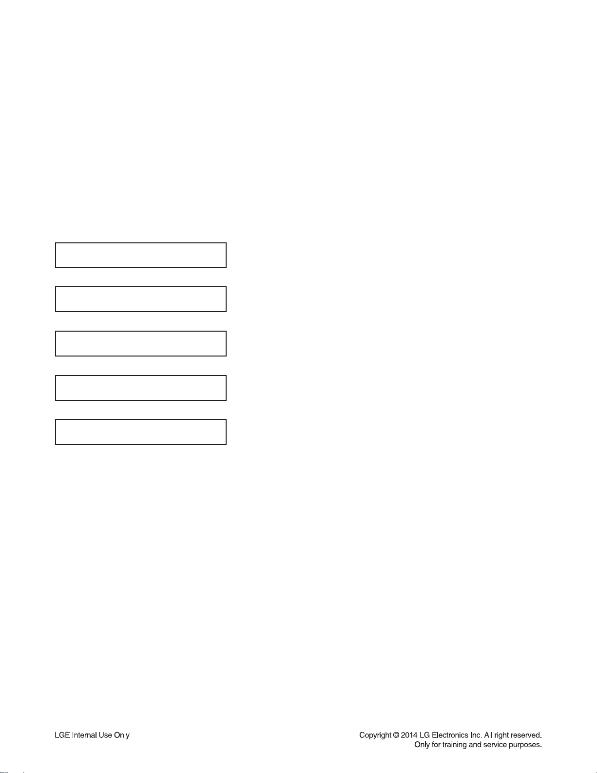
2. MCS PROGRAM
Download program file name must be HG440_OM5540_YYMMDDX.bin
If security program (Water Wall) is activated on your PC, you must save the file to the USB storage device and
disable the security software, then download the file to your set. Downloading file proceeds in the same way at
USB1 function and USB2 function.
Caution: When downloading the file, you should neither unplug the USB device, change to the other function,
nor power off the device.
USB device must be unplugged when the downloading process is completed.
ON VFD DISPLAY SCREEN
NO USB
↓← Insert USB device at USB function.
SEARCH
↓
FIRMWARE
↓
FINISH
↓
Auto POWER OFF
1-7
Page 9
3. EQ PROGRAM
Download program file name must be EQ_PRG.BIN
If security program (Water Wall) is activated on your PC, you must save the file to the USB storage device and
disable the security software, then download the file to your set. Downloading file proceeds in the same way at
USB1 function and USB2 function.
Caution: When downloading the file, you should neither unplug the USB device, change to the other function,
nor power off the device.
USB device must be unplugged when the downloading process is completed.
ON VFD DISPLAY SCREEN
NO USB
↓← Insert USB device at USB function.
SEARCH
↓
EQ UP
↓
FINISH
↓
Auto POWER OFF
1-8
Page 10

SPECIFICATIONS
• GENERAL
Power requirements Refer to the main label.
Power consumption Refer to the main label.
Dimensions (W x H x D) 395.5 mm x 548 mm x 446 mm
Net Weight (Approx.) 16.5 kg
Operating temperature 5 °C to 35 °C (41 °F to 95 °F)
% 09 ot % 5 ytidimuh gnitarepO
Bus Power Supply (USB) 5 V 500 mA
• INPUTS
006 ,zHk 1( smrV 1.2 NI XUA Ω, RCA jack, L/R)
)R/L ,kcaj ø 5.3( smrV 8.0 NI .TROP
Vm 52 NI .CIM
• TUNER
• AMPLIFIER
W 033 latoT
4 ,zHk 1 ta( W 033 onoM tnorF Ω)
% 02 DHT
zHM 00.801 ot 05.78 ro zHM 0.801 ot 5.78 egnaR gninuT MF
Design and specifications are subject to change without notice.
1-9
Page 11

1-10
Page 12

SECTION 2
CABINET & MAIN CHASSIS
CONTENTS
EXPLODED VIEWS ..................................................................................................................................... 2-3
1. CABINET AND MAIN FRAME SECTION (OM5540) ................................................................................ 2-3
2. PACKING ACCESSORY SECTION ......................................................................................................... 2-5
2-1
Page 13
2-2
Page 14
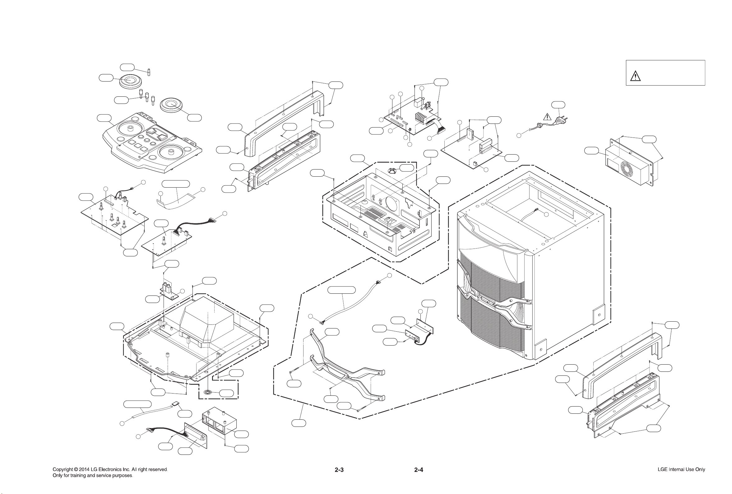
EXPLODED VIEWS
1. CABINET AND MAIN FRAME SECTION (OM5540)
D
L
LED/RCU2
LED
A50
300
I
A
B
I
L
K
K
G
A
D
C
J
J
H
G
E
F
E
H
C
NFC Tag
Bluetooth Module
VFD
MIC
KEY/PTB
KEY/USB
MAIN
SMPS
B
250
250
260
261
264
255
270
262
263
265
A47
A46
251
253
291
513
513
A51
A51
464
464
464
464
464
512
514
512
512
512
512
514
512
464
512
512
A43
A48
A49
A44
A42
254
A53
252
CABLE3
CABLE1
CABLE2
464
464
464
464
464
464
464
464
464
464
NOTES) THE EXCLAMATION POINT WITHIN AN
EQUILATERAL TRIANGLE IS INTENDED
TO ALERT THE SERVICE PERSONNEL
TO THE PRESENCE OF IMPORTANT
SAFETY INFORMATION IN SERVICE
LITERATURE.
Page 15
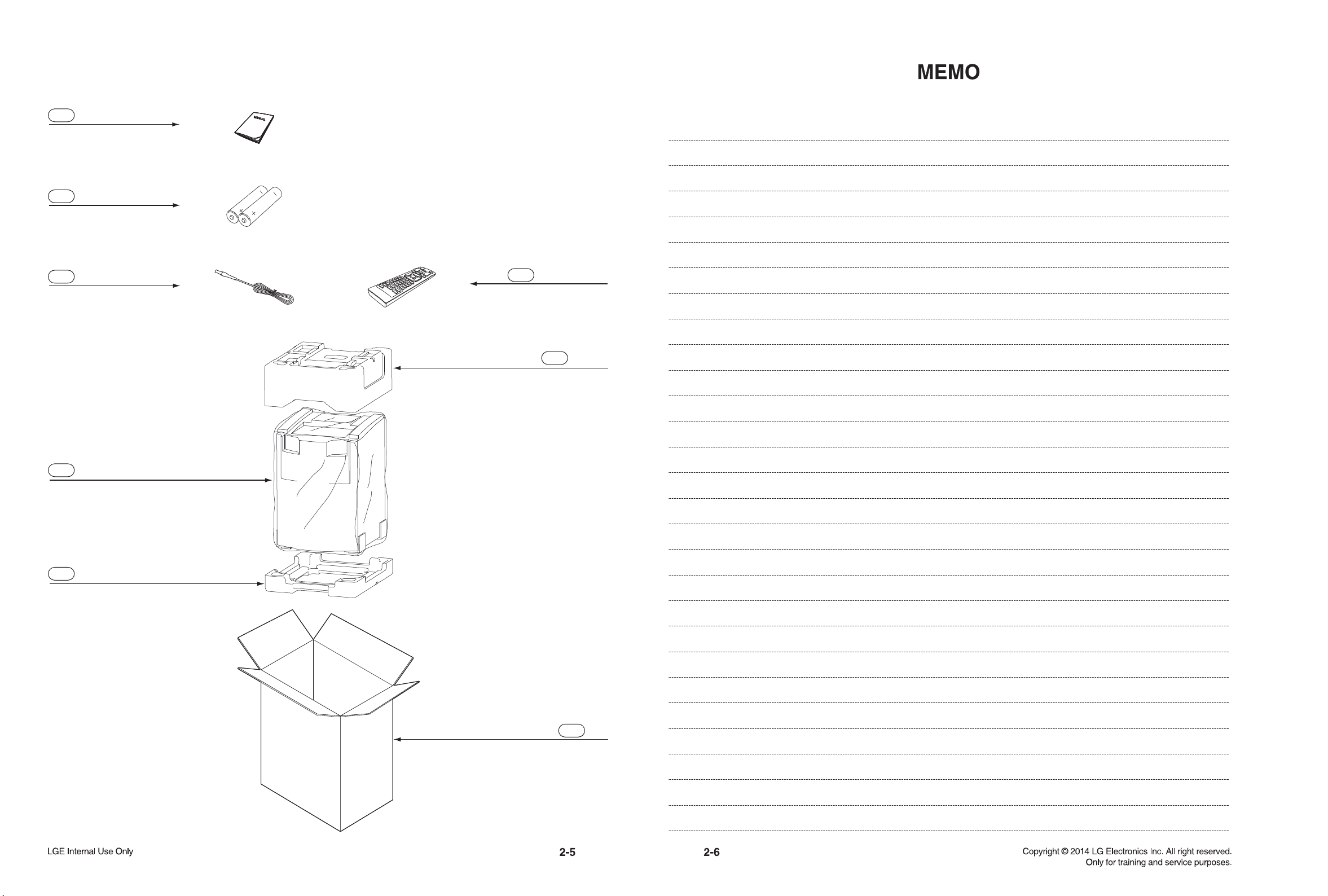
2. PACKING ACCESSORY SECTION
801 Instruction Ass'y
808 Battery
825 FM Wire Antenna
804 Bag
803 Packing
900 Remote Control
803 Packing
802 Box
Page 16

SECTION 3 ELECTRICAL
CONTENTS
ONE POINT REPAIR GUIDE ................................................................................................................... 3-2
1. NO POWER ............................................................................................................................................ 3-2
2. NO BOOTING WHEN POWER ON THE SET ....................................................................................... 3-4
3. VFD IS NOT DISPLAYED WHEN POWER ON THE SET ..................................................................... 3-5
4. NO SOUND ............................................................................................................................................ 3-6
ELECTRICAL TROUBLESHOOTING GUIDE .................................................................................. 3-12
1. POWER (SMPS) ................................................................................................................................... 3-12
2. MCS PART CHECK.............................................................................................................................. 3-15
3. IC504(M24C16) CHECK ....................................................................................................................... 3-15
4. DOUBLE USB FUNCTION ................................................................................................................... 3-16
5. FLD DISPLAY CHECK ......................................................................................................................... 3-17
6. PWM MODULATION CHECK .............................................................................................................. 3-18
7. POWER AMP PART CHECK ............................................................................................................... 3-20
8. TUNER / AUX FUNCTION CHECK ...................................................................................................... 3-21
9. MIC FUNCTION CHECK ...................................................................................................................... 3-22
WAVEFORMS OF MAJOR CHECK POINT ..................................................................................... 3-23
1. SDRAM ................................................................................................................................................. 3-23
2. AUDIO PATH ........................................................................................................................................ 3-23
3. USB....................................................................................................................................................... 3-23
WIRING DIAGRAM ................................................................................................................................... 3-25
BLOCK DIAGRAMS ................................................................................................................................. 3-27
1. SYSTEM BLOCK DIAGRAM_1 ............................................................................................................ 3-27
2. SYSTEM BLOCK DIAGRAM_2 ............................................................................................................ 3-29
3. SMPS BLOCK DIAGRAM_1................................................................................................................. 3-31
4. SMPS BLOCK DIAGRAM_2................................................................................................................. 3-33
CIRCUIT DIAGRAMS ............................................................................................................................... 3-35
1. SMPS CIRCUIT DIAGRAM .................................................................................................................. 3-35
2. MAIN_DSP CIRCUIT DIAGRAM .......................................................................................................... 3-37
3. MAIN_ADC/PWM CIRCUIT DIAGRAM ................................................................................................ 3-39
4. MAIN_AMP CIRCUIT DIAGRAM .......................................................................................................... 3-41
5. FRONT_KEY/USB CIRCUIT DIAGRAM .............................................................................................. 3-43
6. FRONT_VFD CIRCUIT DIAGRAM ....................................................................................................... 3-45
7. FRONT_KEY/PTB CIRCUIT DIAGRAM ............................................................................................... 3-47
8. FRONT_MIC CIRCUIT DIAGRAM ....................................................................................................... 3-49
9. SPK_LED CIRCUIT DIAGRAM ............................................................................................................ 3-51
10. X_LED/RCU2 CIRCUIT DIAGRAM ...................................................................................................... 3-53
CIRCUIT VOLTAGE CHART ................................................................................................................. 3-55
1. ICs......................................................................................................................................................... 3-55
2. CAPACITORS....................................................................................................................................... 3-56
3. CONNECTORS .................................................................................................................................... 3-57
PRINTED CIRCUIT BOARD DIAGRAMS ......................................................................................... 3-59
1. SMPS P.C.BOARD ............................................................................................................................... 3-59
2. MAIN P.C.BOARD ................................................................................................................................ 3-61
3. FRONT_KEY/USB P.C.BOARD ........................................................................................................... 3-63
4. FRONT_VFD P.C.BOARD ................................................................................................................... 3-63
5. FRONT_KEY/PTB P.C.BOARD ........................................................................................................... 3-65
6. FRONT_MIC P.C.BOARD .................................................................................................................... 3-65
7. SPK_LED P.C.BOARD ......................................................................................................................... 3-67
8. X_LED/RCU2 P.C.BOARD ................................................................................................................... 3-67
3-1
Page 17
ONE POINT REPAIR GUIDE
1. NO POWER
If the unit doesn’t work by no power problem, repair the set according to the following
guide.
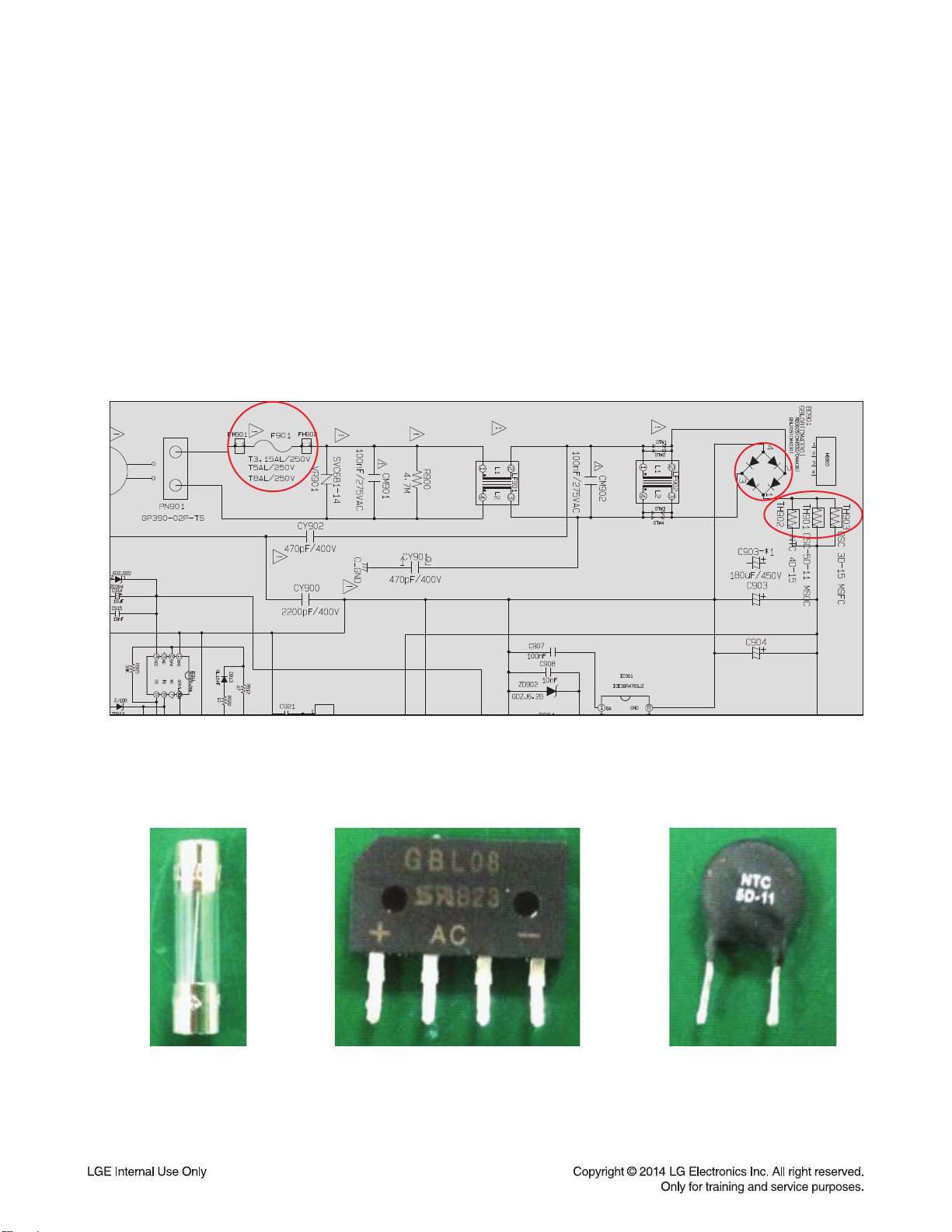
(1) FUSE & BRIDGE DIODE
[ Solution ]
Please check and replace F901, BD901, TH901 or TH903 on SMPS board.
[ How to troubleshoot (Countermeasure) ]
1) Check if the fuse F901 is open or short-circuit.
2) Check if the bridge diode BD901 is short-circuit by over current with a digital multi meter.
3) Check if the NTC thermistor TH901 or TH903 is normal or open.
< SMPS circuit diagram >
[ Service hint (Any picture / Remark) ]
< F901 >
If F901 is not short-circuit,
replace it with a same
specifi cations one.
If BD901 is short-circuit,
replace it with a new one.
< BD901 >
3-2
< TH901 >
If TH901 is open,
replace it with a new one.
Page 18
ONE POINT REPAIR GUIDE
(2) D951
[ Solution ]
Please check and replace D951 on SMPS board.
[ How to troubleshoot (Countermeasure) ]
1) Check the anode-cathod voltage of D951 with a digital multi-meter, it is normally 0.2 ~ 0.3 V.
If it doesn’t have any voltage, it’s destroyed. Replace it with a new one.
[ Service hint (Any picture / Remark) ]
< SMPS circuit diagram >
3-3
Page 19
ONE POINT REPAIR GUIDE
2. NO BOOTING WHEN POWER ON THE SET
The set doesn’t work when press the power button on the front board or the remote
control.
(1) FLASH MEMORY
[ Solution ]
Please check and replace IC503 on MAIN board.
[ How to troubleshoot (Countermeasure) ]
1) Check 5.6 V to CN501 in standby mode.
If there is no 5.6 V, check the SMPS.
2) Check 12 V, F+, F- and PVDD when power on the set.
- If the set doesn’t work regardless of what the KEY1 changes high to low while pressing the power button
X500 and X501 work normally but, if you can not power on the set, replace IC501 with a new one on
the MAIN board.
[ Service hint (Any picture / Remark) ]
PWR_CTRL(R53D)
.
< Main Board Top view >
KEY1(R542)
3-4
Page 20

ONE POINT REPAIR GUIDE
3. VFD IS NOT DISPLAYED WHEN POWER ON THE SET
When power on the set, any icons or characters on VFD are not displayed.
(1) VFD
[ Solution ]
Please check and replace DIG400 on FRONT board.
[ How to troubleshoot (Countermeasure) ]
1) Check if VKK, FL+ and FL- are output from SMPS to VFD via the MAIN board.
2) Check if IC501 outputs VFD_D0, VFD_CLK and VFD_STB to the FRONT board.
3) Check the GR signal(pulse signal) of IC301 on the FRONT board.
Check the SG signal(pulse signal) of IC301 on the FRONT board.
If the GR and SG signal isn’t output, replace IC301 with a new one.
If the GR and SG signal is output, replace DIG302 with a new one.
[ Service hint (Any picture / Remark) ]
GR signal
SG signal
Click the picture,
and then drag to enlarge it.
Check the waveform on details.
GR SIGNAL
ABOUT 30V
SG SIGNAL
ABOUT 30V
3-5
< Waveform of GR and SG signal >
Page 21

ONE POINT REPAIR GUIDE
4. NO SOUND
There is no sound output by DIGITAL AUDIO AMP DAMAGE, repair the set according
to the following guide.
(1) BY DIGITAL AUDIO AMP DAMAGE (IN ALL FUNCTIONS)
[ Solution ]
Please check and replace IC700 on MAIN board.
[ How to troubleshoot (Countermeasure) ]
1) Check PWM_FL± signals from IC601 to IC700 each input function.
If no signal, check if I2S audio signals are entered to IC601.
2) Check the following I2S signal flow. < I2S audio signal Interface >
- MCS_BCK: IC501_Pin E1 --> IC601_Pin23
- MCS_LRCK : IC501_Pin D1 --> IC601_Pin22 (44.1 kHz)
- MCS_DATA_OUT : IC501_Pin E2 --> IC601_Pin24
- MCS_MCLK : IC501_Pin D2 --> IC201_Pin44
If there is any trouble, check the power for each IC. The power is normal but, if the signal waveform to
the IC is distorted or no signal, replace it with a new one.
3) Check PVDD.
If PVDD is abnormal, check the SMPS.
4) Check +12 V for driving the gate of AMP IC.
a. All the powers are normal, but if +12 V is low, there is possible for AMP IC to be damaged.
b. Remove L702, L706 one by one.
When removed a inductance, if +12 V is recovered, the IC connected to it was damaged.
c. Replace the IC with a new one.
5) Check the impedance between IC700_OUT_A/OUT_D & GND.
a. If the impedance is 0 Ω, the IC must be damaged.
b. After removing the heat sink, replace it with a new one.
[ Service hint (Any picture / Remark) ]
DSP IC501
MLC3730
176PIN BGA
< Waveform of I2S audio
interface signals>
FL ±
12.288 MHz
PWM
TAS5548
< I2S signal fl ow >
TAS5631BPHD
< Main Board Top view >
MCS_MCLK (16.93MHz)
MCS_BCK(1.4MHz)
MCS_DATA_OUT
MCS_LRCK(44.1KHz)
L706
L702
3-6
Page 22

ONE POINT REPAIR GUIDE
There is no sound output in the USB FUNCTION, repair the set according to the
following guide.
(2) IN THE USB FUNCTION
[ Solution ]
Please check and replace IC501 on MAIN board & IC460 on USB board.
[ How to troubleshoot (Countermeasure) ]
1) Check +5 V_USB to USB board.
If the USB LED are turned on, the voltage is okay, if so not, check +5.6 V to pin3 of CN460.
2) Check USB D1± or USB D2± from MAIN board to USB board.
a. Check 2.0_D1± signals(pin U7, U8) or 1.1_D1± signals(pin A7, A8) to IC501on MAIN board.
b. Check USB± signals to CN421 (pin 2, 3, 5, 6).
If there is any trouble, check the power for each IC. The power is normal but , if the signal waveform to
the IC is distorted or no signal, replace it with a new one.
3) Check if “Digital audio AMP block” on item 4-(1) is normal.
[ Service hint (Any picture / Remark) ]
DSP IC501
MLC3730
176PIN BGA
12.288 MHz
PWM
TAS5548
FL ±
USB1_D±
USB2_D±
TAS5631BPHD
D- to pin 3&6 of CN421
D+ to pin 2&5 of CN421
< Waveform of USB D± signal >
< USB function signal fl ow >
3-7
Page 23

ONE POINT REPAIR GUIDE
There is no sound output in the AUX FUNCTION, repair the set according to the
following guide.
(3) IN THE AUX FUNCTION
[ Solution ]
Please check and replace IC201 on MAIN board.
[ How to troubleshoot (Countermeasure) ]
1) Check AUX_L/R signals to IC201 (Pin23, 24).
2) Check if MCS_BCK, MCS_LRCK & MCS_MCLK are entered from IC501 to IC201.
3) Check if ADC_DATA is entered from IC201 to IC501.
If no signal, check +5 V & +3.3 V(ADC) for IC201. If is NG, replace it a new one.
4) Check the following I2S signal flow from IC501 to IC601. (Refer to item 4-(1).)
If there is any trouble, check the power for each IC. The power is normal but, if the signal waveform to
the IC is distorted or no signal, replace it with a new one.
5) Check if the digital audio AMP block is okay. Refer to “Digital Audio AMP” guide on Item 4-(1).
If AMP is damaged, replace it with a new one.
[ Service hint (Any picture / Remark) ]
DSP IC501
MLC3730
176PIN BGA
IC201
PWM
CS5346
FL ±
TAS5631BPHD
AUX
AUX_L/R
12.288 MHz
TAS5548
< AUX function signal fl ow >
MCS_LRCK to R219
MCS_MCLK to R220
AUX_R to R227
< Main Board Top view >
MCS_ADC DATA to R215
MCS_BCK to R216
AUX_L to R226
3-8
Page 24

ONE POINT REPAIR GUIDE
There is no sound output in the TUNER FUNCTION, repair the set according to the
following guide.
(4) IN THE TUNER FUNCTION
[ Solution ]
Please check and replace IC201, TU500 on MAIN board.
[ How to troubleshoot (Countermeasure) ]
1) Check if TUNER_LR is entered from Pin1, 3 of TU500 to IC201(Pin26, 27).
If no signals, check +3.3 V for tuner power.
Check if the tuner control signals (CLK, DAT, CE, RST, SLT) are entered from IC501 to TU500.
If it doesn’t work, replace TUNER with a new one.
2) Check if MCS_BCK, MCS_LRCK, & MCS_MCLK are entered from IC501 to IC201.
3) Check if ADC_DATA is entered from IC201 to IC501.
If no signal, check +5 V & +3.3 V(ADC) for IC201. If is NG, replace it with a new one.
4) Check the following I2S audio signal flow from IC501 to IC601. (Refer to item 4-(1).)
If there is any trouble, check the power for each IC. The power is normal but, if the signal waveform to
the IC is distorted or no signal, replace it with a new one.
5) Check if the digital audio AMP block is okay. Refer to “Digital Audio AMP” guide on item 4-(1).
If AMP is damaged, replace it with a new one.
[ Service hint (Any picture / Remark) ]
DSP IC501
MLC3730
176PIN BGA
TUN ER
TUNER_L/R
A
12.288 MHz
TAS5548
< AUX function signal fl ow >
PWM
IC201
CS5346
FL ±
TAS5631BPHD
TUNER_L to C214
< Main Board Top view >
TUNER_R to C215
3-9
Page 25

ONE POINT REPAIR GUIDE
There is no sound output in the PORTABLE FUNCTION, repair the set according to
the following guide.
(5) IN THE PORTABLE FUNCTION
[ Solution ]
Please check and replace IC201 on MAIN board.
[ How to troubleshoot (Countermeasure) ]
1) Check PT_L/R signals to IC201 (Pin9, 10).
2) Check if MCS_BCK, MCS_LRCK, & MCS_MCLK are entered from IC501 to IC201.
3) Check if ADC_DATA is entered from IC201 to IC501.
If no signal, check +5 V & +3.3 V(ADC) for IC201. If NG, replace it a new one.
4) Check the following I2S signal flow from IC501 to IC601. (Refer to item 4-(1).)
If there is any trouble, check the power for each IC. The power is normal but, if the signal waveform to
the IC is distorted or no signal, replace it with a new one.
5) Check if the digital audio AMP block is okay. Refer to “Digital Audio AMP” guide on Item 4-(1).
If AMP is damaged, replace it with a new one.
[ Service hint (Any picture / Remark) ]
DSP IC501
MLC3730
176PIN BGA
PTB_L/R
Porta ble
12.288 MHz
TAS5548
PWM
IC201
CS5346
FL ±
TAS5631BPHD
< PORTABLE function signal fl ow >
PTB_L to R229
PTB_R to R228
< Main Board Top view >
3-10
Page 26

ONE POINT REPAIR GUIDE
There is no sound output in the MIC FUNCTION, repair the set according to the
following guide.
(6) IN THE MIC FUNCTION
[ Solution ]
Please check and replace IC203 on MAIN board and IC420 on front MIC board.
[ How to troubleshoot (Countermeasure) ]
1) Check MIC_SIG signal, from JACK421, JACK422 to IC420 (Pin3) on front MIC board.
2) Check MIC_SIG signal from IC420 (Pin4) to CN423.
If no signal, check +5 V for IC420. If NG, replace it a new one.
3) Check MIC_SIG signal from CN423 (Pin4) to CN420.
4) Check if MCS_BCK, MCS_LRCK, & MCS_MCLK are entered from IC501 to IC203.
5) Check if ADC_DATA is entered from IC203 to IC501.
If no signal, check +5 V & +3.3 V(ADC) for IC203. If NG, replace it a new one.
6) Check the following I2S signal flow from IC501 to IC601.(Refer to item 4-(1).)
If there is any trouble, check the power for each IC. The power is normal but, if the signal waveform to
the IC is distorted or no signal, replace it with a new one.
7) Check if the digital audio AMP block is okay. Refer to “Digital Audio AMP” guide on item 4-(1).
If AMP is damaged, replace it with a new one.
[ Service hint (Any picture / Remark) ]
DSP IC501
MLC3730
mic1
MIC SIG
mic2
IC420
S4308
12.288 MHz
PWM
TAS5548
MIC SIG
IC203
AK5358
FL ±
176PIN BGA
TAS5631BPHD
3.3V to L240
MCS_SIG to R218
5V to L241
MCS_ADC DATA to R243
< Main Board Top view >< MIC function signal fl ow >
MCS_LRCK to R241
MCS_MCLK to R240
MIC_SIG to R217
MCS_BCK to R242
3-11
Page 27

ELECTRICAL TROUBLESHOOTIHG GUIDE
1. POWER (SMPS)
No 5.6 VA
F901 normal? Replace F901 (Use the same fuse).
BD901 normal? Replace BD901.
TH901(TH903) normal? Replace TH901.
YES
NO
YES
NO
YES
NO
YES
Is Vcc
(10 V ~ 18 V) supplied to
IC901 Pin7?
YES
NO
D902 normal?
NO
Check or replace D902.
NO
D933 / D934 normal? Replace D933 / D934.
YES
Is there
about 2.5 V at
NO
Replace IC941.
IC941 Pin1?
YES
NO
D935 normal? Replace D935.
YES
NO
D932 normal? Replace D932.
YES
D931 normal? Replace D931.
YES
Power line of main PCB is short.
NO
3-12
Page 28

ELECTRICAL TROUBLESHOOTIHG GUIDE
No PVDD
YES
F901 normal? Replace F901 (Use the same fuse).
YES
BD901 normal? Replace BD901.
YES
TH901(TH903) normal? Replace TH901.
YES
NO
NO
NO
Is Vcc
(10 V ~ 18 V) supplied to
IC911 Pin4?
YES
NO
D903 normal?
YES
Q911 base "H"?
YES
•
Check P-CTRL "H" signal from MCS.
• Check PC902.
Check or replace Q911.
Q901 normal? Replace Q901.
YES
D951 normal? Replace D951.
NO
NO
NO
Check or replace D903.
NO
YES
Is there about 2.5 V
at IC951 Pin1?
YES
Power line of main PCB is short.
NO
Replace IC951.
3-13
Page 29

ELECTRICAL TROUBLESHOOTIHG GUIDE
No 12 V
YES
Is Vcc (15 V)
supplied to IC931?
YES
IC931 Pin4 “H”?
YES
Check or replace IC931.
No VFD
YES
D931 normal?
NO
NO
NO
Check or replace D935.
Check the ‘P.CTL “H”’ signal from μ-com
Check or replace D931.
YES
ZD931 normal?
YES
Q501 / Q502 normal?
YES
Check or replace VFD.
NO
NO
3-14
Check or replace ZD931.
Check or replace Q501 / Q502.
Page 30

ELECTRICAL TROUBLESHOOTIHG GUIDE
2. MCS PART CHECK
MCS PART CHECK
YES
Check if
voltage of CN501 Pin7, 8
is 5.6 VA.
YES
Check if IC510
have 3.3 V output.
YES
Check if IC508
have 1.2 V output.
YES
X500: 32.768 kHz,
X501: 24 MHz,
Check the operation.
NO
NO
NO
Refer to
SMPS troubleshooting.
Check and change IC510.
Check and change IC508.
YES
OK
3. IC504(M24C16) CHECK
CHECK IC501 PIN.
YES
Check pinC2, pinB1
DATA : CLK
YES
OK OK
NO
Check MCS
voltage 3.3 VA.
YES
Check MCS.
YES
3-15
NO
Refer to MCS troubleshooting.
NO
Replace MCS.
Page 31

ELECTRICAL TROUBLESHOOTIHG GUIDE
4. DOUBLE USB FUNCTION
USB FUNCTION
YES
Plug-in usb device.
YES
Display “NO USB”.
YES
Display “READ”.
YES
Display “NO FILE”.
YES
Check usb audio fi le in usb device
(MP3, WMA fi le is playable)
Check USB_5 V.
YES
Check USB
D+/D-
YES
Check IC501
(Pin U7, U8, A7, A8).
NONO
NO
NO
Check CN421.
Check USB jack
(CN461/ CN462).
Replace IC501.
3-16
Page 32

ELECTRICAL TROUBLESHOOTIHG GUIDE
5. FLD DISPLAY CHECK
FLD DISPLAY CHECK
YES
Check
CN501 Pin13,14,15 input
voltage.
YES
Check if both end voltage
of FL+, FL- are over 2.9 V
VKK : over 25.6 V.
YES
Check CN400
connection and power
Pin1, 2, 3(FL+, FL-, VKK),
Pin9(3.3 V).
YES
Check
IC400(MC3401) voltage
Pin30 VKK: -25.8 V
Pin13, 43: 3.3 V.
NO
Refer to SMPS troubleshooting.
NO
Check CN400 connection.
YES
Check each
Pin voltage.
YES
OK
NO
If voltage is not 3.3 V.
YES
YES
Check
IC501->IC400
data communication
STB/ DATA/ CLK
YES
FLD light on?
YES
OK
Check IC400.
YES
OK
NO
Check input data
IC501 Pin F1, F2, G1.
YES
Check output data IC501 Pin D2.
YES
Check IC501.
YES
OK
3-17
NO
Replace IC400.
NO
Replace IC501.
Page 33

ELECTRICAL TROUBLESHOOTIHG GUIDE
6. PWM MODULATION CHECK
PWM MODULATION PART CHECK
YES
Check
CN501 Pin7,8
(5.6 V)
YES
• Check IC601(TAS5548)
VDD 3.3 V - Pin9, 14, 35, 50.
• Check X601 (12.288 MHz).
YES
Check
X601(12.288 MHz)
operation.
YES
Check
IC601 Pin21 CLK
input.
NO
NO
Refer to
SMPS troubleshooting.
Check X601
(12.288 MHz).
YES
OK
NO
Replace X601(12.288 MHz).
YES
Check IC501
(MLC3730)
Pin B3: RESET
Pin A1: SDA
Pin A2: SCL
output.
YES
A
NO
Check line
resistor output
RST: R53E / SCL: R53C /
SDA: R53B.
YES
OK
3-18
NO
Replace R53E,R53C,R53B.
Page 34

ELECTRICAL TROUBLESHOOTIHG GUIDE
A
YES
Check
IC601(TAS5548)
input data
Pin24
PWM wave.
YES
Check PWM
modulator output
FL: Pin48(-), 49(+)
FR: Pin46(-), 47(+).
Other output
check.
NO
NO
Check
IC601 DATA
input.
YES
OK
Check IC601.
YES
NO
Check each line resistor output.
NO
Replace
IC601.
OK
YES
OK
3-19
Page 35

ELECTRICAL TROUBLESHOOTIHG GUIDE
7. POWER AMP PART CHECK
POWER AMP PART CHECK
YES
Check CN501
Pin10: 12 V
Pin1,2,3: 48 V.
YES
Check IC701
Pin25, 26, 55, 56 input voltage.
YES
Check IC700
Pin2, 6, 55: 12 V.
YES
Check IC700 Pin4, 5 input voltage.
YES
Check IC700 Pin28, 29, 52, 53 input voltage.
NO
Refer to SMPS troubleshooting.
NO
Check each line resistor output voltage.
YES
Check output
line coil.
YES
OK
NO
Replace the coil.
3-20
Page 36

ELECTRICAL TROUBLESHOOTIHG GUIDE
8. TUNER / AUX FUNCTION CHECK
FUNCTION CHECK
YES
Check IC201
(CS5346) Pin23, 24,
26, 27 input.
YES
Check IC201
(CS5346) Pin41 output
data.
YES
Check
IC501(MLC3700)
input data.
YES
IC501(MLC3730)
output data.
NO
Check JK200, TU500.
Check IC201
Pin5: +3.3 V
Pin14: +5 V.
YES
Check IC201
Pin5: +3.3 V,
Pin6: High,
Pin14: +5 V.
NONO
Check CN501 Pin7, 8: +5.6 V.
Check IC201
NONO
Pin41: SDOUT,
Pin42: SLCK,
Pin43: LRCK,
Pin44: MCLK.
Replace IC201.
YES
OK
YES
3-21
Page 37

ELECTRICAL TROUBLESHOOTIHG GUIDE
9. MIC FUNCTION CHECK
MIC FUNCTION
CHECK
YES
Check
IC420(S4308) pin3
input.
YES
Check
IC420(S4308) pin4
data output.
YES
Check
IC203(AK5358) pin1, 2
data input.
NO
NO
NO
Check JK421, JK422.
Check IC420
pin6: +5 V
YES
Check
IC203 pin5: +5 V
pin5: +3.3 V
NO
NO
Check CN501 pin7, 8: +5.6 V.
NO
Check IC423
pin1: +5 V.
YES
Replace IC201.
NO
Check IC203
PIN9: SCLK PIN10: MLCK
PIN11: LRCK
PIN12: ADC_DATA
YES
IC501(MLC3730) data output.
YES
OK
3-22
YES
YES
Page 38

1. SDRAM
WAVEFORMS OF MAJOR CHECK POINT
1
2
3
4
2. AUDIO PATH
5
6
CLK
DATA
ADDRESS
CS
DAC_MCLK
DAC_BCK
IC502 Pin38
IC502 Pin53
IC502 Pin35
IC203 Pin19
IC501 Pin D2
IC501 Pin E1
3. USB
7
8
9
10
USB_5V
D+
D-
DAC_LRCK
DAC_DATA
IC501 Pin D1
IC501 Pin E2
IC501 Pin A8
IC501 Pin A7
3-23
Page 39

3-24
Page 40

3-25 3-26
VFD
FR-1
MAIN
(FR-4 EPOXY 2LAYER)
Wire Harness 15P
SMPS
(CEM-3 )
BT
FFC 10P
Wire Harness 15P
Front & KEY 1
FR-1
FFC 29P
FFC 10P
Wire Harness 12P
Wire
Harness
7P
Front & KEY 2
FR-1
FFC 29P
FCC 10P
FCC 10P
USB
Wire Harness 12P
VFD&IR
MIC & PTB
LED
AMP 2P
MIC
IR,X_LED
Wire Harness 7P
Wire Harness 4P
Wire Harness 4P
Wire Harness 5P
Wire Harness 5P
WIRING DIAGRAM
Page 41

3-27 3-28
BLOCK DIAGRAMS
1. SYSTEM BLOCK DIAGRAM_1
MLC3730
1.2/3.3V
PWM
TAS5548DGG
PWM_MUTE
PWM_RST
MCS_LRCK/BCK/
DATA_OUT
AMP
TAS5631BPHD
12.288M
AMP_PDN
AMP_SD/OTW / PROTECT/ CLIP0(FRONT_AGL)
24M
32.768K
S4308
Mic 1
Mic 2
ADC
CS5346
PORTABLE
TUNER
AUX1
PTB_SENSE
MCS_MCLK/LRCK/BCK
ADC_DATA
MIC_SENSE
BT_TX/RX/RTS/
CTS/RST
BT
Module
MB8811C0
EAT61876201
PNZ-EAJ58881201CN039533-AP01
MC3401
u-COM
MCS_TX/RX/CS
VFD_CS/CLK/DO
VFD
Jog 4ea
SPK_LED
KEY1,2 / VOL_A/B
FRONT1
SPK LED
FRONT2
KST-MWOO4MV0-S71W
EBL60720702
KEY3/DRV_VBUS2.0
LM37102D
USB1.1
USB2.0 OTG
2.0_D+/D-
1.1_D+/D-
IR
VFD
REMOCON
Debug_Console_IN/OUT
JTAG
NTRST/TDI/TMS/TCK/TDO/CHIP_RESET/RTCK
Console (TP)
3.7VA
AZ7027RTRE1
CHIP_RESET
MCS_RTC_3.0A
AZ7027RTRE1
P_SENSE
VFD_PWR_CTRL
PWR_CTRL
SMPS/
LDO’S
R5F100GEAFB
MICOM_RESET
SEARCH_A/B
Jog 1ea
MIC_VOL_A/B
BASS_VOL_A/B
TRAB_VOL_A/B
MEAS_VOL_A/B
ADC_RST
BT_CLK/DAT
Jog 1ea
REMOCON
AMP_READY
PWM_DAT/CLK
SDRAM
8MB
M12L64164A
M0 0~15
A 00~11
S.FLASH
4MB
W25Q64F
Main : 0IMMREB004H(M12L64164A)
SF_CS/SCK/MISO/
MOSI
Sub : EAN60700802(W9864G6JH)
W BT : EAN62459301 (4MB)
W/O BT : EAN55718402 (1MB)
EEPROM
2KB
M24C16
EEPROM
SCL/SDA
ADC_CLK/DAT
Page 42

2. SYSTEM BLOCK DIAGRAM_2
3-29 3-30
SDRAM
(8MB)
Serial Flash
(4MB)
DB[0-15]
DMA[0-10]
2.0 D+, D-
TUNER L/R
PORT L/R
BT
PORTABLE
MLC3730
(176PIN)
24 MHz
3.3/5V
3.3V/1.2V
3.3V
SPI
I2C,RESET
I2C
3.3V
3.3V
VFD Driver
MC3501
IR
3.3V
FL+,FL-
Vkk
Key_1
FUNCTION KEY * 10 EA
LPF
PWM
TAS5548
AMP
TAS5631B
3.3V
CTL
I2C
12.288 MHz
PVDD(48V)/GVDD(12V)
TUNER
(AM/FM)
DAC_MCLK / BCK
/ LRCK / DAC_DATA
AUX L/R
AUX
Mic
Mic L/R
Mic AMP
S4308
Tuner
1.1 D+, D-
I2C
EEPROM
(2KByte)
3.3V
AMP_SD/OTW / PROTECT/ CLIP0
32.768 KHz
BT_SCL/SDA/TX/RX/RTS/CTS/RST
FRONT1 PCB
I/O U-COM
LC87FC096AVU
Volume * 3 EA
3.3V/5V
Main
VR
VFD PCB
USB 1
USB 2
MAIN + AMP PCB
SPK LED PCB
IR
Key_2
KEY cont
3.3V/12V
SPI
Key_3
USB REC KEY * 1 EA
FRONT2 PCB
3.3V/5V
Search
VR
3.3V
MIC JACK PCB
SPI
PORTABLE
Mic
M.Vol Jack 1
Jack 2
DRV_VBUS
LED
RED LED
Volume cont
USB 1
USB 2
Key_3
12V
ADC
(CS5346)
Page 43

3. SMPS BLOCK DIAGRAM_1
3-31 3-32
++12
V
SMPS
+5
.6V
A
FAN X 1
TU50
0
TUNER
YST996
IC504
EEPROM
24C
S16
IC601
TAS5548
IC50
1
MCS
MLC3730
IC502
SDRAM
6
4
M
b
RF IC
I
C509
AZ1117
US
B
HUB
SMSC
IC400
MC3
4
0
1
VFD DRV
RMC
1.2VA
IC51
0
FLASH
32Mb
IC
510
LDO
AZ111
7
FRONT B’
d
U
SB
P
W
R
LM3710
2D
MOTOR
AM3
053
S
DV
CC_5V
+3.7VA
V
F
D
5m
A
3m
A
160mA
25mA
40mA
+5V
3
70m
A
LE
D
STBY
20mA
2
mA
2.2
~ 2
.
6A
1
00m
A
45
0mA
Pi
ck u
p
8
0mA
80m
A
1
0mA??
130mA
-> 0
mA
2
0mA
2
0mA??
160mA??
A
D
C
IC201
CS534
6
41m
A
VKK
FL
±
51mA
1A
273m
A
Bluetoot
h
O
ption
25mA
CP Chip
O
ption
7m
A
IC700
AMP
TA
S5631BPH
D
IC202
LDO
LM37102D
IC507
LDO
TJ3965
IC506
RESET
AZ
702
7
IC50
5
PWR SE
NS
AZ702
7
2m
A
2mA
23m
A
DVCC_3.3
V
8
0
m
A?
U
SB HUB
IC509
AZ11
17
USB HUB
M
CS
_
1.2V
50m
A?
37
4
mA
P
WR_CTRL
3
8mA?
UBS2.0_OTG_V
BUS
(MLC37
3
0)
DRV_VBUS2.0
3.3V
A
MCS_RTC_3.0A
V
D
D30
RTC
(MLC3730)
120m
A
2mA?
IC5
01
u
- COM
2
3mA
283m
A
P
WR_CTRL
25mA
SPK
LED B’d
(16ea)
160mA
360mA
5
6m
A
368mA
1
.4
A
65
%
60
%
65
%
50
%
MIC AMP
IC
42
0
S43
08
10m
A
VFD
FRONT1
FRONT2
SPK
LED
Page 44

4. SMPS BLOCK DIAGRAM_2
3-33 3-34
PVDD
+
Noise
Filter
Block
(X-cap
Line Filter)
Snubber
Block
Main
SMPS IC
Block
T
R
A
N
S
Snubber
Block
Photo coupler
Photo coupler
Photo coupler
FL+
FL-
Vkk
On/Off
12V LDO
12 V
5.6 VA
P.CTL
On/Off
AMP
SMPS IC
With FET
Block
F
U
S
E
Y-Cap
Y-Cap
T
R
A
N
S
CN901
Feedback
Feedback
Page 45

3-35 3-36
CIRCUIT DIAGRAMS
1. SMPS CIRCUIT DIAGRAM
IMPORTANT SAFETY NOTICE
WHEN SERVICING THIS CHASSIS, UNDER NO
CIRCUMSTANCES SHOULD THE ORIGINAL DESIGN BE
MODIFIED OR ALTERED WITHOUT PERMISSION
FROM THE LG CORPORATION. ALL COMPONENTS
SHOULD BE REPLACED ONLY WITH TYPES IDENTICAL
TO THOSE IN THE ORIGINAL CIRCUIT. SPECIAL
COMPONENTS ARE SHADED ON THE SCHEMATIC
FOR EASY IDENTIFICATION.
THIS CIRCUIT DIAGRAM MAY OCCASIONALLY DIFFER
FROM THE ACTUAL CIRCUIT USED. THIS WAY,
IMPLEMENTATION OF THE LATEST SAFETY AND
PERFORMANCE IMPROVEMENT CHANGES INTO
THE SET IS NOT DELAYED UNTIL THE NEW SERVICE
LITERATURE IS PRINTED.
NOTE :
1. Shaded(
) parts are critical for safety.
Replace only with specified part number.
2. Voltages are DC-measured with a digital voltmeter
during Play mode.
A
1
2
3
4
5
6
7
8
9
10
11
12
B C D E F G H I J K L M N O P Q R ST
CAUTION:
Danger if fuse is incorrectly replaced.
Replace only with the type identical to fuse rating
and(or) model name described in main label.
Warning
Parts that are shaded are critical with
respect to risk of fire or electrical shock.
SMPS
EAX65422801-SD_Rev0_1.0_Working
2014. 02. 21
Page 46

3-37 3-38
2. MAIN_DSP CIRCUIT DIAGRAM
A
1
2
3
4
5
6
7
8
9
10
11
12
B C D E F G H I J K L M N O P Q R ST
MAIN_DSP
EAX65685801-SD(#01)_Rev7_1.6
2014. 02. 21
Page 47

3-39 3-40
3. MAIN_ADC/PWM CIRCUIT DIAGRAM
A
1
2
3
4
5
6
7
8
9
10
11
12
B C D E F G H I J K L M N O P Q R ST
MAIN_ADC/PWM
EAX65685801-SD(#02)_Rev7_1.6
2014. 02. 21
Page 48

3-41 3-42
4. MAIN_AMP CIRCUIT DIAGRAM
A
1
2
3
4
5
6
7
8
9
10
11
12
B C D E F G H I J K L M N O P Q R ST
MAIN_AMP
EAX65685801-SD(#03)_Rev7_1.6
2014. 02. 21
Page 49

3-43 3-44
5. FRONT_KEY/USB CIRCUIT DIAGRAM
A
1
2
3
4
5
6
7
8
9
10
11
12
B C D E F G H I J K L M N O P Q R ST
FRONT_KEY/USB
EAX65667301-SD_Rev14_1.5
2014. 02. 21
Page 50

3-45 3-46
6. FRONT_VFD CIRCUIT DIAGRAM
A
1
2
3
4
5
6
7
8
9
10
11
12
B C D E F G H I J K L M N O P Q R ST
FRONT_VFD
EAX65668701-SD_Rev14_1.5
2014. 02. 21
Page 51

3-47 3-48
7. FRONT_KEY/PTB CIRCUIT DIAGRAM
A
1
2
3
4
5
6
7
8
9
10
11
12
B C D E F G H I J K L M N O P Q R ST
FRONT_KEY/PTB
EAX65689401-SD_Rev14_1.6
2014. 02. 21
Page 52

3-49 3-50
8. FRONT_MIC CIRCUIT DIAGRAM
A
1
2
3
4
5
6
7
8
9
10
11
12
B C D E F G H I J K L M N O P Q R ST
FRONT_MIC
EAX65689601-SD_Rev14_1.5
2014. 02. 21
Page 53

3-51 3-52
9. SPK_LED CIRCUIT DIAGRAM
A
1
2
3
4
5
6
7
8
9
10
11
12
B C D E F G H I J K L M N O P Q R ST
SPK_LED
EAX65690301-SD_Rev9_1.5
2014. 02. 21
Page 54

3-53 3-54
10. X_LED/RCU2 CIRCUIT DIAGRAM
A
1
2
3
4
5
6
7
8
9
10
11
12
B C D E F G H I J K L M N O P Q R ST
X_LED/RCU2
EAX65632101-SD_Rev4_1.3
2014. 02. 21
Page 55

3-55 3-56
CIRCUIT VOLTAGE CHART
1. ICs 2. CAPACITORS
Designator Description Polarity (+) Polarity (-)
OM5540 FRONT
C460 Capacitor,Ceramic,Chip 5.57 0
C462 Capacitor,Ceramic,Chip 5.11 0
OM5540 MIC
C429 Capacitor,AL,Radial 5.03 0
C430 Capacitor,AL,Radial 2.02 0
OM5540 VFD
C401 Capacitor,AL,Radial 3.28 0
C410 Capacitor,AL,Radial 3.19 0
OM5540 SPK LED
C483 Capacitor,AL,Radial 3.18 0
OM5540 MAIN
C501 Capacitor,AL,Chip 3.28 0
C508 Capacitor,AL,Chip 3.28 0
C526 Capacitor,AL,Chip 1.19 0
C591 Capacitor,AL,Chip 3.23 0
C706 Capacitor,AL,Chip 12.19 0
C714 Capacitor,AL,Radial 48.7 0
C731 Capacitor,AL,Radial 48.7 0
C244 Capacitor,AL,Chip 5.03 0
C618 Capacitor,AL,Chip 3.28 0
C624 Capacitor,AL,Chip 12.18 0
C643 Capacitor,AL,Chip 5.03 0
Designator PIN Number Description Part Site Specifi cation SPEC
REAL
VALUE
CHECK
LOC.
IC101 48
IC,Microcontrollers
R5F100GHAFB
Supply Voltage(VDD) 3.10~3.50 3.28 L108
IC201
6,35,46
IC,A/D Converter
CS5346
Core Supply Voltage(VDD) 3.13~3.46 3.27 C231
14 PLL Supply Voltage(VDDA) 4.8~5.2 5.03 C229
IC202
IN 5.6VA
IC,LDO Voltage Regulator
TJ4220GDP-ADJ 6.5V ADJ 0W SOP R/TP 8P
- TAEJIN TECHNOLOGY CO., LTD.
5.6V±0.2 5.65
-
OUT 5VU 5V±0.2 5.03
IC203
6
IC,A/D Converter
AK5358
Supply Voltage(VDD) 4.8~5.2 5.03 C242
5 PLL Supply Voltage(VDDA) 3.13~3.46 3.28 C241
IC501
J4
IC, DIGITAL SIGNAL PROCESSORS
MLC3730
Core Supply Voltage(VDD12INT) 1.08~1.32 1.18 C517
A9,E9,J14,U4 Core Supply Voltage(VDD12CORE) 1.08~1.32 1.18 C535
T10 Core Supply Voltage(VDD12ALIVE) 1.08~1.32 1.18 C542
P12 Core Supply Voltage(VDD12PLL) 1.08~1.32 1.19 C548
P9 Core Supply Voltage(VDD12USB20) 1.08~1.32 1.19 C538
A10,D4,D14,P4,P14 IO Supply Voltage(VDD33IO) 3.00~3.60 3.28 C524
U9 IO Supply Voltage(VDD33OSC) 3.00~3.60 3.28 C539
A4 IO Supply Voltage(VDD33ADC) 3.00~3.60 3.28 C527
B7 IO Supply Voltage(VDD33USB11) 3.00~3.60 3.28 C531
U5,U6 IO Supply Voltage(VDD33xUDB20) 3.00~3.60 3.28 C532
T16 VDD30RTC 2.75~3.30 3.23 C545
IC502 1,3,9,14,27,43,49,
IC,SDRAM
M12L64164A-5TG2Y 64MBIT
Core Supply Voltage(VDD) 3.13~3.46 3.29 -
IC503 8
IC,Serial Flash Memory
Supply Voltage(VDD) 3.13~3.46 3.29 C554
IC505 -- - -
3.63
-
3.00
IC507
IN 5.6VA
IC,LDO Voltage Regulator
AZ1117BH-1.2TRE1 15V 1.2V 0W S OT-223 R/TP 3P
- BCD
5.6V±0.2 4.86
-
OUT VCC_5V 5V±0.2 3.28
IC508
IN 3.3VA
IC,LDO Voltage Regulator
LM37102D 2.25V TO 16V ADJ 770m W SOP R/TP 8P
- TAEJIN TECHNO LOGY CO., LTD.
3.3V±0.15 3.29
-
OUT VDD12 1.2V±0.1 1.20
IC510
IN 5.0VA
IC,LDO Voltage Regulator
AZ1117BH-ADJTRE1 15V ADJ 0W SOT223 R/TP 3P
- BCD
4.8V±0.3 4.87
-
OUT 3.3VA 3.3V±0.15 3.29
IC601
14,35,50
IC,Sound/Audio Processor
TAS5548
Core Supply Voltage(VDD) 1.71~1.89 3.27 C612
9 PLL Supply Voltage(VDDA) 3.13~3.46 3.28 C611
IC700
25,26,55,56,64
IC,Audio Amplifi er
TAS5631
Supply Voltage(VDD) 11.8~13.3 12.0 L706
30,31,38,39,42,43,50,51 PVDD Supply Voltage(VDDA) 45.6~50.4 48.7 C734
Page 56

3-57 3-58
3. CONNECTORS
No. PIN NAME Output Voltage SPEC
CN400
1 FL+ -18.11
2 FL- -20.77
3 Vkk -23.42
4 DGND 0
5 VFD_DO
6 VFD_CLK
7 VFD_CS
8 DGND 0
9 3.3VA 3.28
10 REMOCON
CN421
1 DGND 0
2 D1_P
3 D1_M
4 DGND 0
5 D2_P
6 D2_M
7 5.6VA 5.65
8 KEY3 3.28
9 USB_P_CTRL 3
10 SEARCH_A 3.27
11 SEARCH_B 3.27
12 DGND 0
CN422
1 DVCC_5V 5.03
2 MIC SENSE
3 MIC SIG
4 AGND
CN482
1 3.3VA 3.29
2 REMOCON
3 DGND
4 W LED
5 12V 12.05
CN501
1 PVDD 46.7 43.7 ~ 48.3
2 PVDD 46.7 43.7 ~ 48.3
3 PVDD 46.7 43.7 ~ 48.3
4 DGND 0
5 DGND 0
6 DGND 0
7 5.6VA 5.69 5.4 ~ 5.8
8 5.6VA 5.69 5.4 ~ 5.8
9 DGND 0
No. PIN NAME Output Voltage SPEC
10 12V 12.19 11.4 ~ 12.6
11 PWR-CTRL 2.23 3.1 ~ 3.4
12 DGND 0
13 VKK -23.54 -23 ~ -29
14 FL- -20.84 -20.1 ~ -24.4
15 FL+ -18 -17.5 ~ -22.1
CN502
1 DGND 0 0
2 KEY2 3.28 2.5 ~ 2.75
3 DGND 0 0
4 TRAB_VOL A 3.28 2.8 ~ 3.3
5 TRAB_VOL B 3.28 2.8 ~ 3.4
6 DGND 0 0
7 MEAS_VOL A 3.28 3.1 ~ 3.5
8 MEAS_VOL B 3.28 3.1 ~ 3.5
9 BASS_VOL A 3.28 3.1 ~ 3.5
10 BASS_VOL B 3.28 3.1 ~ 3.5
11 DGND 0 0
12 KEY1 3.28 3.1 ~ 3.5
13 DGND 0 0
14 MIC_VOL_A 3.28 3.1 ~ 3.5
15 MIC_VOL_B 3.28 3.1 ~ 3.5
16 DGND 0 0
17 MAIN_VOL A 3.28 3.1 ~ 3.5
18 DGND 0 0
19 MAIN_VOL B 3.28 3.1 ~ 3.5
20 AGND 0 0
21 MIC SIG 3.28 3.1 ~ 3.5
22 MIC SENSE 3.28 3.1 ~ 3.5
23 AGND 0 0
24 PTB_R
25 AGND 0 0
26 PTB_L
27 PTB SENSE 3.3 3.1 ~ 3.5
28 DVCC_5V 5 4.8 ~ 5.2
29 AGND 0 0
CN504
1 VDD 3.27
2 RESET 3.28
3 CTS
4 RTS
5 RXD
6 GND 0
7 TXD
8 GND 0
No. PIN NAME Output Voltage SPEC
9 SCL
10 SDA
CN507
1 12V 12,19
2 DGND 0
3 W LED
4 SPK LED
5 IR2
6 DGND 0
7 3.3VA 3.28
Page 57

3-59 3-60
PRINTED CIRCUIT BOARD DIAGRAMS
1. SMPS P.C.BOARD
(TOP VIEW)
(BOTTOM VIEW)
NOTE) Warning
Parts that are critical with respect to risk
of fire or electrical shock.
Page 58

3-61 3-62
2. MAIN P.C.BOARD
(TOP VIEW)
(BOTTOM VIEW)
Page 59

3-63 3-64
3. FRONT_KEY/USB P.C.BOARD
(TOP VIEW)
4. FRONT_VFD P.C.BOARD
(TOP VIEW)
(BOTTOM VIEW)
(BOTTOM VIEW)
Page 60

3-65 3-66
5. FRONT_KEY/PTB P.C.BOARD
(TOP VIEW)
6. FRONT_MIC P.C.BOARD
(TOP VIEW)
(BOTTOM VIEW)
(BOTTOM VIEW)
Page 61

3-67 3-68
7. SPK_LED P.C.BOARD
(TOP VIEW)
8. X_LED/RCU2 P.C.BOARD
(TOP VIEW)
(BOTTOM VIEW)
(BOTTOM VIEW)
 Loading...