

Page 1

LCD Projection Monitor
SERVICE MANUAL
CAUTION
BEFORE SERVICING THE CHASSIS,
READ THE SAFETY PRECAUTIONS IN THIS MANUAL.
CHASSIS : RE-01JB
MODEL : MW-60SZ12
website:http://biz.LGservice.com
e-mail:http://www.LGEservice.com/techsup.html
Page 2

Contents . . . . . . . . . . . . . . . . . . . . . . . . . . . . . . . . . . . . . . . . . . . . . . . . . . . . . . . . 2
Safety Precautions . . . . . . . . . . . . . . . . . . . . . . . . . . . . . . . . . . . . . . . . . . . . . . . . 3
Servicing Precautions. . . . . . . . . . . . . . . . . . . . . . . . . . . . . . . . . . . . . . . . . . . . . . 4
Electrostatically Sensitive (ES) Devices. . . . . . . . . . . . . . . . . . . . . . . . . . . . . . . . 4
Description of Controls. . . . . . . . . . . . . . . . . . . . . . . . . . . . . . . . . . . . . . . . . . . . . 5
Adjustment Instructions . . . . . . . . . . . . . . . . . . . . . . . . . . . . . . . . . . . . . . . . . . . . 9
Correction of Screen Tilt & Keystone. . . . . . . . . . . . . . . . . . . . . . . . . . . . . . . . . 13
Replacing the Lamp. . . . . . . . . . . . . . . . . . . . . . . . . . . . . . . . . . . . . . . . . . . . . . . 16
Description of each Block Circuits. . . . . . . . . . . . . . . . . . . . . . . . . . . . . . . . . . . 17
Description of Micom . . . . . . . . . . . . . . . . . . . . . . . . . . . . . . . . . . . . . . . . . . . . . 25
Block Diagram . . . . . . . . . . . . . . . . . . . . . . . . . . . . . . . . . . . . . . . . . . . . . . . . . . . 33
Exploded View. . . . . . . . . . . . . . . . . . . . . . . . . . . . . . . . . . . . . . . . . . . . . . . . . . . 34
Exploded View Parts List . . . . . . . . . . . . . . . . . . . . . . . . . . . . . . . . . . . . . . . . . . 35
Replacement Parts List . . . . . . . . . . . . . . . . . . . . . . . . . . . . . . . . . . . . . . . . . . . . 36
Schematic Diagram . . . . . . . . . . . . . . . . . . . . . . . . . . . . . . . . . . . . . . . . . . . . . . . . .
- 2 -
Contents
Page 3

Safety Precautions
- 3 -
1. Before returning an instrument to the customer, always make a safety check
of the entire instrument, including, but not limited to, the following items:
a. Be sure that no built-in protective devices are defective and/or have been
defeated during servicing. (1) Protective shields are provided on this chassis to protect both the technician and the customer. Correctly replace all
missing protective shields, including any removed for servicing convenience. (2) When reinstalling the chassis and/or other assemblies in the
cabinet, be sure to put back in place all protective devices, including, but
not limited to, nonmetallic control knobs, insulating fishpapers, adjustment
and compartment covers/shields, and isolation resistor/capacitor networks.
Do not operate this instrument or permit it to be operated without all
protective devices correctly installed and functioning.
b. Be sure that there are no cabinet openings through which an adult or child
might be able to insert their fingers and contact a hazardous voltage. Such
openings include, but are not limited to, (1) spacing between the picture
tube and the cabinet back, (2) excessively wide cabinet ventilation slots,
and (3) an improperly fitted and/or incorrectly secured cabinet back cover.
c. Antenna Cold Check-With the instrument AC plug removed from any AC
source, connect an electrical jumper across the two AC plug prongs. Place
the instrument AC switch in the on position. Connect one lead of an ohmmeter to the AC plug prongs tied together and touch the other ohmmeter
lead in turn to each tuner antenna input exposed terminal screw and, if
applicable, to the coaxial connector. If the measured resistance is less than
1.0 megohm or greater than 5.2 megohm, an abnormality exists that must
be corrected before the instrument is returned to the customer. Repeat this
test with the instrument AC switch in the off position.
d. Leakage Current Hot Check-With the instrument completely reassembled,
plug the AC line cord directly into a 120 V AC outlet.
(Do not use an isolation transformer during this test.) Use a leakage current
tester or a metering system that complies with American National Standards
Institute (ANSI) C101.1 Leakage Current for Appliances and Underwriters
Laboratories (UL) 1410, (50.7). With the instrument AC switch first in the on
position and then in the off position, measure from a known earth ground
(metal waterpipe, conduit, etc.) to all exposed metal parts of the instrument
(antennas, handle bracket, metal cabinet, screwheads, metallic overlays,
control shafts, etc.), especially any exposed metal parts that offer an electrical return path to the chassis. Any current measured must not exceed 0.5
milliamp. Reverse the instrument power cord plug in the outlet and repeat
the test.
ANY MEASUREMENTS NOT WITHIN THE LIMITS SPECIFIED HEREIN
INDICATE A POTENTIAL SHOCK HAZARD THAT MUST BE ELIMINATED BEFORE RETURNING THE INSTRUMENT TO THE CUSTOMER.
e. X-Radiation and High Voltage Limits-Because the picture tube is the pri-
mary potential source of X-radiation in solid-state TV receivers, it is specially constructed to prohibit X-radiation emissions. For continued X-radiation
protection, the replacement picture tube must be the same type as the original. Also, because the picture tube shields and mounting hardware perform
an X-radiation protection function, they must be correctly in place.
High voltage must be measured each time servicing is done that involves
B+, horizontal deflection, or high voltage. Correct operation of the X-radiation protection circuits also must be reconfirmed each time they are serviced. (X-radiation protection circuits also may be called “horizontal disable”
or “hold-down.”) Read and apply the high voltage limits and, if the chassis is
so equipped, the X-radiation protection circuit specifications given on instrument labels and in the Product Safety & X-radiation Warning note on the
service data chassis schematic.
High voltage is maintained within specified limits by close-tolerance safetyrelated components/adjustments in the high-voltage circuit.
If high voltage exceeds specified limits, check each component specified on
the chassis schematic and take corrective action.
2. Read and comply with all caution and safety-related notes on or inside the
receiver cabinet, on the receiver chassis, or on the picture tube.
3. Design Alteration Warning- Do not alter or add to the mechanical or electrical design of this TV receiver. Design alterations and additions, including,
but not limited to, circuit modifications and the addition of items such as
auxiliary audio and/or video output connections, might alter the safety characteristics of this receiver and create a hazard to the user. Any design alterations or additions will void the manufacturer’s warranty and will make you,
the servicer responsible for personal injury or property damage resulting
therefrom.
4. Picture Tube Implosion Protection Warning-The picture tube in this
receiver employs integral implosion protection. For continued implosion protection, replace the picture tube only with one of the same type and number. Do not remove, install, or otherwise handle the picture tube in any
manner without first putting on shatterproof goggles equipped with side
shields. People not so equipped must be kept safely away while picture
tubes are handled. Keep the picture tube away from your body. Do not handle the picture tube by its neck. Some “in-line” picture tubes are equipped
with a permanently attached deflection yoke; because of potential hazard,
do not try to remove such “permanently attached” yokes from the picture
tube.
5. Hot Chassis Warning-a. Some TV receiver chassis are electrically connected directly to one conductor of the AC power cord and may be safely
serviced without an isolation transformer only if the AC power plug is inserted so that the chassis is connected to the ground side of the AC power
source. To confirm that the AC power plug is inserted correctly, with an AC
voltmeter measure between the chassis and a known earth ground. If a
voltage reading in excess of 1.0 V is obtained, remove and reinsert the AC
power plug in the opposite polarity and again measure the voltage potential
between the chassis and a known earth ground. b. Some TV receiver chassis normally have 85 V AC (RMS) between chassis and earth ground
regardless of the AC plug polarity. These chassis can be safely serviced
only with an isolation transformer inserted in the power line between the
receiver and the AC power source, for both personnel and test equipment
protection. c. Some TV receiver chassis have a secondary ground system
in addition to the main chassis ground. This secondary ground system is
isolated from the AC power line. The two ground systems are electrically
separated by insulating material that must not be defeated or altered.
6. Observe original lead dress. Take extra care to assure correct lead dress in
the following areas: a. near sharp edges, b. near thermally hot parts- be
sure that leads and components do not touch, c. the AC supply, d. high
voltage, and e. antenna wiring. Always inspect in all areas for pinched, outof-place, or frayed wiring. Do not change spacing between components,
and between components and the printed circuit board. Check the AC
power cord for damage.
7. Components, parts, and/or wiring that appear to have overheated or are
otherwise damaged should be replaced with components, parts, or wiring
that meet original specifications. Additionally, determine the cause of overheating and/or damage and, if necessary, take corrective action to remove
any potential safety hazard.
8. PRODUCT SAFETY NOTICE
Some electrical and mechanical parts have special safety related characteristics which are often not evident from visual inspection, nor can the protection they give necessarily be obtained by replacing them with components
rated for higher voltage, wattage, etc. Parts that have special safety characteristics are identified by shading, by a
*
, or by on schematics and
parts lists. Use of a substitute replacement that does not have the same
safety characteristics as the recommended replacement parts might create
shock, fire, and/or other hazards. Product safety is under review continuously and new instructions are issued whenever appropriate.
AC Leakage Test
DEVICE
UNDER
TEST
TEST ALL
EXPOSED MET AL
SURFA CES
2-WIRE CORD
ALSO TEST WITH
PLUG REVERSED
(USING AC ADAPTER
PLUG AS REQUIRED)
LEAKAGE
CURRENT
TESTER
+ -
(READING SHOULD
NO T BE ABOVE
0.5mA)
EAR TH
GROUND
Page 4

Servicing Precautions
- 4 -
CAUTION: Before servicing instruments covered by this service manual and
its supplements, read and follow the SAFETY PRECAUTIONS section of this
manual. Note: If unforeseen circumstances create conflict between the following servicing precautions and any of the safety precautions, always follow the
safety precautions. Remember: Safety First.
General Servicing Precautions
1. a. Always unplug the instrument AC power cord from the AC power source
before: (1) removing or reinstalling any component, circuit board, module,
or any other instrument assembly. (2) disconnecting or reconnecting any
instrument electrical plug or other electrical connections. (3) connecting a
test substitute in parallel with an electrolytic capacitor in the instrument.
Caution: Awrong part substitution or incorrect polar-ity installation of
electrolytic capacitors may result in an explosion hazard.
b. Do not defeat any plug/socket B+ voltage interlocks with which instru-
ments covered by this service manual might be equipped.
c. Do not apply AC power to this instrument and/or any of its electrical
assemblies unless all solid-state device heat sinks are correctly installed.
d. Always connect a test instrument’s ground lead to the instrument chassis
ground before connecting the test instrument positive lead.
Always remove the test instrument ground lead last.
Note: Refer to the Safety Precautions section of this manual.
2. The service precautions are indicated or printed on the cabinet, chassis, or
components. When servicing, follow the printed or indicated service precautions and service materials.
3. The components used in the unit have a specified flame resistance and
dielectric strength. When replacing any components, use components
which have the same ratings. Components identified by shading, by
*
, or
by in the circuit diagram are important for safety or for the characteristics
of the unit. Always replace with the exact replacement components.
4. An insulation tube or tape is sometimes used and some components are
raised above the printed wiring board for safety. The internal wiring is sometimes clamped to prevent contact with heating components. Install them as
they were.
5. After servicing, always check that the removed screws, components, and
wiring have been installed correctly and that the portion around the service
part have not been damaged. Further, check the insulation between the
blades of the attachment plug and accessible conductive parts.
INSULATION CHECKING PROCEDURE
Disconnect the attachment plug from the AC outlet and turn the power on.
Connect the insulation resistance meter (500 V) to the blades of the attachment plug. The insulation resistance between each blade of the attachment
plug and accessible conductive parts (Note 1) should be more than 1 Mohm.
Note: Accessible conductive parts include metal panels, input terminals, earphone jacks, etc.
Electrostatically Sensitive (ES) Devices
Some semiconductor (solid-state) devices can be damaged easily by static electricity. Such components commonly are called
Electrostatically Sensitive (ES) Devices. Examples of typical ES
devices are integrated circuits and some field-effect transistors
and semiconductor “chip” components. The following techniques
should be used to help reduce the incidence of component damage caused by static electricity.
1. Immediately before handling any semiconductor component
or semiconductor-equipped assembly, drain off any electrostatic charge on the body by touching a known earth ground.
Alternatively, obtain and wear a commercially available discharging wrist strap device, which should be removed for
potential shock reasons prior to applying power to the unit
under test.
2. After removing an electrical assembly equipped with ES
devices, place the assembly on a conductive surface such as
aluminum foil, to prevent electrostatic charge buildup or exposure of the assembly.
3. Use only a grounded-tip soldering iron to solder or unsolder
ES devices.
4. Use only an anti-static solder removal device. Some solder
removal devices not classified as “anti-static” can generate
electrical charges sufficient to damage ES devices.
5. Do not use freon-propelled chemicals. These can generate
electrical charge sufficient to damage ES devices.
6. Do not remove a replacement ES device from its protective
package until immediately before you are ready to install
t.(Most replacement ES devices are packaged with leads electrically shorted together by conductive foam, aluminum foil, or
comparable conductive material.)
7. Immediately before removing the protective material from the
leads of a replacement ES device, touch the protective material to the chassis or circuit assembly into which the device will
be installed.
Caution: Be sure no power is applied to the chassis or circuit,
and observe all other safety precautions.
8. Minimize bodily motions when handling unpackaged replace
ment ES devices. (Otherwise, seemingly harmless motion,
such as the brushing together of your clothing or the lifting of
your foot from a carpeted floor, can generate static electricity
sufficient to damage an ES device.)
Page 5

- 5 -
Description of Controls
Main Body
Main Body
ON/OFF
ON/OFF
ON/OFF Button
SOURCE MENU VOLENTER
MENU Button
SOURCE Button ENTERA / Button
/
VOL
F, G Button
Indicators
E, D Button
* Temperature indicator, lamp Indicator and operation indicator at the front of the monitor show the user the
operating status of the monitor.
Orange Standby.
Green(flashing) Lamp cooling untill the lamp turn on.
Operation Indicator
Lamp Indicator
Temperature Indicator
“ ”
is the warning message on screen.
Green On operation.(Turn on the lamp)
Orange(flashing) Monitor lamp is cooling as power out(1 minutes)
Off Power off.
Red to be replaced with a new lamp.(over 10000 hours)
Red(flashing)
Green(flashing) The lamp cover is not closed.
Red
Red(flashing) Power has turned off due to problem with the
Green(flashing) internal cooling fans. Contact your service center.
(for 25 seconds)(Refer to P.18)
Monitor lamp is reaching the end of its life and needs
“Replace the Lamp”
The monitor has trouble in the lamp or around it.
Contact the service center.
The monitor is turned off due to its high temperature.
Contact your service center.
Page 6

- 6 -
Rear Connecting Part
Rear Connecting Part
RGB IN3(DVI-I)
(12V/0.5A)
RGB IN1 RGB IN2 RGB OUT
DC OUT
RGB IN3
(DVI-I)
VIDEOS-VIDEO
RS-232C
RS-232C
PONENT
COM-
YPBPR
RL
MOUSE
MIC
RGB IN1
RGB IN2
RGB OUT
MOUSE
RS-232C
RGB IN1 RGB IN2 RGB OUT
RGB IN3(DVI-I)
(12V/0.5A)
VIDEOS-VIDEO
RS-232CRGB IN3(DVI-I)
PONENT
MOUSE
MIC
DC OUT
COM
R L
MIC
DC OUT(12V/0.5A)
*Use this jack when
connecting the
wireless receiver to
the monitor.
S-VIDEO
VIDEO
YPBPR
COMPONENT
B, PR)
(Y, P
R, L
Page 7

- 7 -
POWER
SOURCE
MENU
L
R
ZOOM
MUTE
LASER
Remote Control
MOUSE DRAG
VOL.
STILL
ARC
AUTO
AVL
DASP
APC
MIC
Remote Control
POWER Button
SOURCE Button
MENU Button
MOUSE DRAG
L MOUSE Button
(Zoom-out Button)
ENTERA Button
ZOOM Button
LASER Button
R MOUSE Button
(Zoom-in Button)
POINTER Button
MUTE Button
* Switches the sound
on or off.
Button
VOL. +, - Button
STILL Button
ARC Button
AUTO Button
AVLButton
DASP Button
APC Button
MIC Button
Button
Button
Function
Function
POWER Button Selects ON/OFF of power.
SOURCE Button Switches to RGB1/2/3, Video, S-Video, Component mode.
MENU Button Displays or hides the menu.
L MOUSE Button * Corresponds to the Left - Click of PC Mouse.
(Zoom-out Button) * Downsizes the screen on the zoom function.
R MOUSE Button * Corresponds to the Right - Click of PC Mouse.
(Zoom-in Button) * Enlarges the screen size on zoom function.
POINTER Button * After selecting menus, controls selecting and adjusting
functions with the direction of up, down, left, right.
* Moves the screen with the direction of up, down, left, right
on zoom function.
* Moves and releases the selected icon on PC screen.
MOUSE DRAG Button Uses to select and drag an icon in PC mode.
ENTERA Button Checks the present mode and sets the change of functions.
ZOOM Button Refer to page 34.
MUTE Button Cuts off audio.
VOL.(+, -) Button Adjusts volume level.
STILL Button
ARC Button
AUTO Button
AVL Button
DASP Button
APC Button
MIC Button
LASER Button Projects a bright red laser point on to the screen for indication
purposes.
(Don’t look at laser beam directly as it will cause eye
damage.)
Page 8

- 8 -
Accessories
Accessories
POWER
MENU
SOURCE
L
R
ZOOM
MUTE
LASER
Remote Control
1.5V
1.5V
Batteries 2 (size AA)
Audio/Video Cable
DVI cable
Computer Cable
Mouse Connecting Cables
PS/2 Mouse Cable
(IBM PC or Compatible)
Optional Extras
* Contact your dealer for buying these items.
* Contact your dealer for replacing a new lamp.
S-Video Cable
Lamp
Operating guide
MAC Serial Mouse Cable
Page 9

1. Application Object
This instruction is for the application to the LCD projection Monitor.
2. Notes
(1) The power source insulation of this LCD Projection TV is
not charging type and you may not use the transformer for
insulation. But you better adjust the set after operating it
with insulation transformer between power supply cable
and input part of the set for protecting the adjusting equipment.
(2) The adjustment must be performed under the correct
sequence.
(3) The adjustment must be performed in the circumstance of
25!5°C of temperature and 65!10% of relative humidity if
there is no specific designation.
(4) The input voltage of the receiver must keep 220V, 60Hz in
adjusting.
(5) The set must be operated for 5 minuets preliminarily
before adjustment if there is no specific designation.
The preliminary operation must be performed after receiving 100% white pattern, but reception of the moving picture may also be possible in unavoidable case.
3. DRIVER Voltage Adjustment
All adjustment mode are entered by pressing the IN-START
key on the remote control, after adjustment press the ENTER
key to come out.
(1) Required Test Equipment
1) Output voltage measurement Jig : 1EA
2) PC Patteren generator : 1EA
3) Aremote control for adjustment
(2) Setting of Devices
(3) Preparation for Adjustment
1) Connect the PC pattern Generator with the RE-01JB set
as Fig.1
2) Adjust the PC pattern generator to XGA60Hz.
3) Press the INPUT SELECTION key(TV/AV) to select the
RGB1 input.
4) Install the Main Board of RE-01JB to the set JIG.
(4) Sequence of Adjustment (VREF&VMID)
1) Turn the set on.
2) Use the IN-START key on the R/C for adjustment to select
'Drive LCCOM Adjust' in adjustment menu.
3) Adjust voltage of VREF and VMID for each R,G,B. ( SEE a
Table below)
4) Press the ENTER key on the R/C for adjustment to store
the adjustment value when adjustment is finished.
4. EPLD Programming
(1) Required Test Equipment
1) Byteblaster
2) PC (or Notebook): 1EA
3) EPLD Program
(2) Sequence of Adjustment
1) Connect one port of Byteblaster to the Parallel Port and
connect another port of Byteblaster to P1201 of Sound
Board.
2) Turn the SET and PC on.
3) Operate an EPLD program of PC(or Notebook).
5. Signal adjustment of LCD control
5-1. LCCOM ADJUSTMENT
(1) Required Test Equipment
1) Pattern generator which can generate each R,G,B signal
of fined horizontal bar pattern.
2) Aremote control for adjustment : 1EA
(2) Sequence of Adjustment
1) Turn on the power supply of JIG for adjustment.
2) Adjust the PC pattern generator to XGA60Hz and fined
horizontal bar pattern and then connect to the SET.
3) Press the INPUT SELECTION key on the R/C to select
RGB.
4) Press IN-START key on the R/C for adjustment to enter
adjustmet mode.
5) Select LCCOM adjustment menu.
6) Use the VOLUME key to make the fewest screen FLICKER with watching screen. (Adjust individually after
inputting each RGB input signal.)
7) Press the ENTER key to come out of adjustment mode
when adjustment is finished.
5-2. NRS ADJUSTMENT
(1) Required Test Equipment
1) PC Pattern generator : 1EA
2) Aremote control for adjustment : 1EA
(2) Sequence of Adjustment
1) Turn the Power supply on.
2) Adjust the PC pattern generator to XGA60Hz and 16Gray
pattern and then connect the PC pattern generator to SET.
3) Press the INPUT SELECTION key on the R/C to select
RGB.
Adj.Value
The minimum value which is over 9.5V
7.0V
VREF
VMID
IC1808 PIn 14
IC1808 PIn1
- 9 -
Adjustment Instructions
R G B
(fig. 1) Voltage adjustment Set
MONITOR
Voltage
measurement
JIG
RGB
Board
SET JIG
PC Pattern
Generator
Page 10

4) Press the IN-START key on the R/C for adjustment to
enter adjustment mode.
5) Select NRS adjustment menu.
6) Use the VOLUME key to make the fewest vertical lines on
the screen with watching screen.
7) Press the ENTER key to come out of adjustment mode
when adjustment is finished.
6. Factory Default&RGB Gain/Offset
Adjustment
(1) Required Test Equipment
1) Pattern generator : 1EA
2) Aremote control for adjustment : 1EA
(2) Sequence of Adjustment
1) Adjust the pattern generator to white/black window as Fig.
Below and connect to RGB1 Input terminal of the set.
2) Select RGB1 as Input signal.
3)Press the IN-START key on the R/C for adjustment to enter
adjustment mode and select Factory Default in adjustment
mode.
4) Press the ENTER key to operate Factory Default and enter
adjustment mode again and then select AutoGain in
adjustment menu.
5) Press the ENTER key to operate AutoGain and press the
Enter key to store AutoGain when adjustment is finished.
7. Screen Position Adjustment
(1) Required Test Equipment
1) Pattern generator : 1EA
2) Aremote control for adjustment : 1EA
(2) Sequence of Adjustment
1) Connect a power source with TV Set and turn TV Set on.
2) Do heat run for 5 min and over before adjustment.
3) Input the farthest outer pattern signal into pattern genera-
tor except DTV signal (Hat or Hatch pattern which has the
farthest line) and connect to RGB1 and then select Input
signal of set to RGB1.
4) Press IN-START key on the remote control to enter the
adjustment mode.
5) Select POSITION CONTROL of adjustment menu and
then select the H POSITION in SUB Menu.
6) Adjust H-Position so that the farthest line is shown and to
be symmetrical on the end of right/left screen.
7) Select the V POSITION in Menu.
8) Adjust V POSITION so that the farthest line is shown and
to be symmetrical on the end of top/bottom screen.
9) When finishing the adjustment, get out of adjustment mode
by pressing ENTER button on Remote Control.
7. White Balance &Gamma Adjustment
(1) Required Test Equipments
1) Illuminometer (name of model : CA-100) : 1EA —>
Measure color of projecting screen center
2) Pattern Generator : 1EA —> 16 step Gray Pattern, 64 step
Gray Pattern
3) Aremote control for adjustment : 1EA
(2) Setting of Devices
7-1 Sequence of Gamma manually adjustment
1) Prepare the PC Pattern Generator which is possible to output R/G/B of 16 step and 64 step Gray Pattern.
2) Equipment composition : Follow Fig. 3.
3) Turn on the Jig for adjustment.
4) Select the RGB 1 by pressing the input select button on
Remote Control.
5) Output the 16 Gray Pattern in PC Pattern Generator.
Check it with the naked eye whether Screen Gamma and
W/B is right about each Gray.
If it’s not, press the IN-START button on Remote Control
and then adjust the level data of each step manually in
sub menu of Gamma RGB.
6) Output the 64 Gray Pattern in PC Pattern Generator.
Check it with the naked eye whether Screen Gamma and
W/B is right about each Gray or whether there is Gamma
noise.
If there’s any problem, press the IN-START button on
Remote Control and then adjust the level data of each
step manually in sub menu of Gamma RGB.
7) After finishing adjustment, exit adjustment mode by using
ENTER button on Remote Control.
7-2 Sequence of Gamma Auto Adjustment
1) Display the biggest WHITE PATTERN on screen and
change the 7050 R/G/B CONTRAST ( or 16th Gamma 1
R/G/B) data value of adjustment mode so that the white
balance of illumination system or illuminometer to be
x:283, y: 297(D9300K).
2) Measure the luminance value with changed data value in
clause 1.
3) Seek the luminance of each step so that each Gamma
value of 16 step to be 2.5 curve on a basis of luminance
value measured in clause 2. ( Maximum luminance *
(n1/16)** Maximum luminance : luminance measured
in clause 2)
N 1 : Each step unit (1.2.3.4,------15) when classify the signal level to 16 step.
4) Input the Gray pattern corresponding to the first luminance
and change the first adjustment mode R/G/B data value so
that the R/G/B data value to be same white balance with
1) above and luminance with 3) above.
- 10 -
PC Pattern
Generator
MW-60SZ12
Page 11

- 11 -
5) Input the Gray pattern corresponding to the second luminance and change the second adjustment mode R/G/B
data value of Gamma adjustment item so that the R/G/B
data value to be same white balance with 1) and right to
the second luminance (measured in clause 3)
6) Input pattern signal with same method above and change
the Gamma R/G/B data value of corresponding level and
make same luminance with 3) and white balance with 1).
9. Uniformity Adjustment
(1) Required Test Equipments
1) Uniformity measurement equipment
2) ARemote Control for Adjustment
3) PC Pattern Generator : 1EA
(2) Setting of Devices
(3) Sequence of Adjustment
1) Adjust the screen coordinates as shown below.
2) Output the 17th VDP Test Pattern signal(7050 MAX 640) of
No. 4 sub adjustment item maximum adjustment.
Read the white coordinates and communicate 3 line with
ET7050 IC through measurement equipment of optics.
Adjust screen coordinates data to adjust the color uniformity of max point.
At this time, make sure that deviation is +5~-5% and standard is color coordinate of center.
3) Output the 16th VDP Test Pattern signal(7050 MID 570) of
No. 4 sub adjustment item(middle adjustment).
Read the white coordinates and communicate 3 line with
ET7050 IC through measurement equipment of optics.
Adjust screen coordinates data to adjust the color uniformity of mid point.
At this time, make sure that deviation is +5~-5% and standard is color coordinate of center.
4) Output the 15th VDP Test Pattern signal(7050 MIN 360) of
No. 4 sub adjustment item(min adjustment).
Read the white coordinate and communicate with ET7050
IC through measurement equipment of optics.
Adjust screen coordinates data to adjust the color unifor-
mity of miner point.
At this time, make sure that deviation is +5~-5% and standard is color coordinate of center.
5) White the miner, middle, maximum data for each point to
confront to each MICOM address.
10. Video Gain Adjustment
(1) Required Test Equipments
1) TV
2) ARemote Control for Adjustment
(2) Sequence of Adjustment
1) Press the INPUT SELECTION key on the R/C to select
VIDEO input.
2) Input the NTSC 13CH signal into Video input.
3) Set the set input to video (AV input).
4) Press the IN-START key on R/C for adjustment to select
'2101 Color Control1' in adjustment menu.
5) Raise the 2101 picture value to the maximum(63).
6) Use the 2101 subbright value and adjust upper 3 gradation
of Gray bar not to be distinguished.
7) Set the video channel to NTSC 6CH.
8) Press the IN-START key on R/C for adjustment again to
select '2101 Color Control1' in adjustment menu.
9) Raise the Driver G Gain to the maximum(63) and then
stop the Driver G Gain when the US 6CH is visible.
10) Make the Driver B value same with Driver G value and
make the Driver R value higher(2) than Driver G.
11) Press the ENTER key on R/C for adjustment to store the
adjustment value when the adjustment is finished.
0 1 2 3 ............xx..........15 16
1
.
yy
.
11
12
Adj.Jig
Camera
MW-60SZ12
PC Pattern
Generator
Adjust 3 gradations
not to be
distinguished.
Color Bar
Gray Bar
Adjust the these
letters not to
be saturated.
US 6CH
Page 12

11. Component Gain Adjustment
(1) Required Test Equipments
1) Signal(DTV Signal 31-3)
2) SET-TOP box( or an equipment which can generate YPbPr
output receiving DTV signal)
3) ARemote Control for Adjustment
(2) Sequence of Adjustment
1) Press the TV/AV key on the R/C for adjustment to select
component input.
2) Input DTV signal 31-3 into component input.
3) Press the IN-START key on the R/C for adjustment to
select '2101 color control1' in menu.
4) Raise the 2101 picture value to the maximum.
5) Use the 2101 subbright value and adjust lower 2 gradation
of Gray bar not to be distinguished.
6) Press the IN-START key on R/C for adjustment again to
select '2101 color control2' in adjustment menu.
7) Use the Driver G Gain and adjust 2101 G Gain so that all
gradation(11gradation) of upper Gray bar are distinguished.
8) Make the Driver B value same with Driver G value and
make the Driver R value higher(2) than Driver G.
9) Press the ENTER key on R/C for adjustment to store the
adjustment value when the adjustment is finished.
12. EDID Data INput
(1) Required Test Equipments
1) AJIg for adjusting PC,DDC.(PC serial to D-sub.connection
equipment)
2) SW for writing DDC(EDID data write & read)
3) D-sub terminal
4) D-sub /DVI conversion connector
(2) Setting of Devices
(3) Preparation for Adjustment
1) Set devices as above and turn the PC,jig on.
2) Put the S/W for writing DDC(EDID datawrite&read)into
operation.(Operated in DOS mode.)
(4) Sequence of Adjustment
1) Turn the set on and set the input to RGB1 and then connect D-sub to RGB1 input terminal.
2) nput the product code, production week/year, serial number (if it is not input, write "01") to the S/W for writing DDC.
3) Select '60RPM_A' out of DDC file.
4) Operate the EDID write command and check the
60RPM_A is writed well through the Read command.
5) Connect the DVI conversion connector to D-sub and
RGB3(DVI) input terminal of set.
6) Set the Input selection to RGB3.
7) Select '60RPM_D' out of DDC file.
8) Operate the EDID Write command and check the
60RPM_D is writed well through the Read command.
- 12 -
Adjust 2101 G Gain
so that all lumination
are distinguished.
Adjust subbright
so that 2 lumination
are not to be
distinguished.
PC
JIG
Page 13
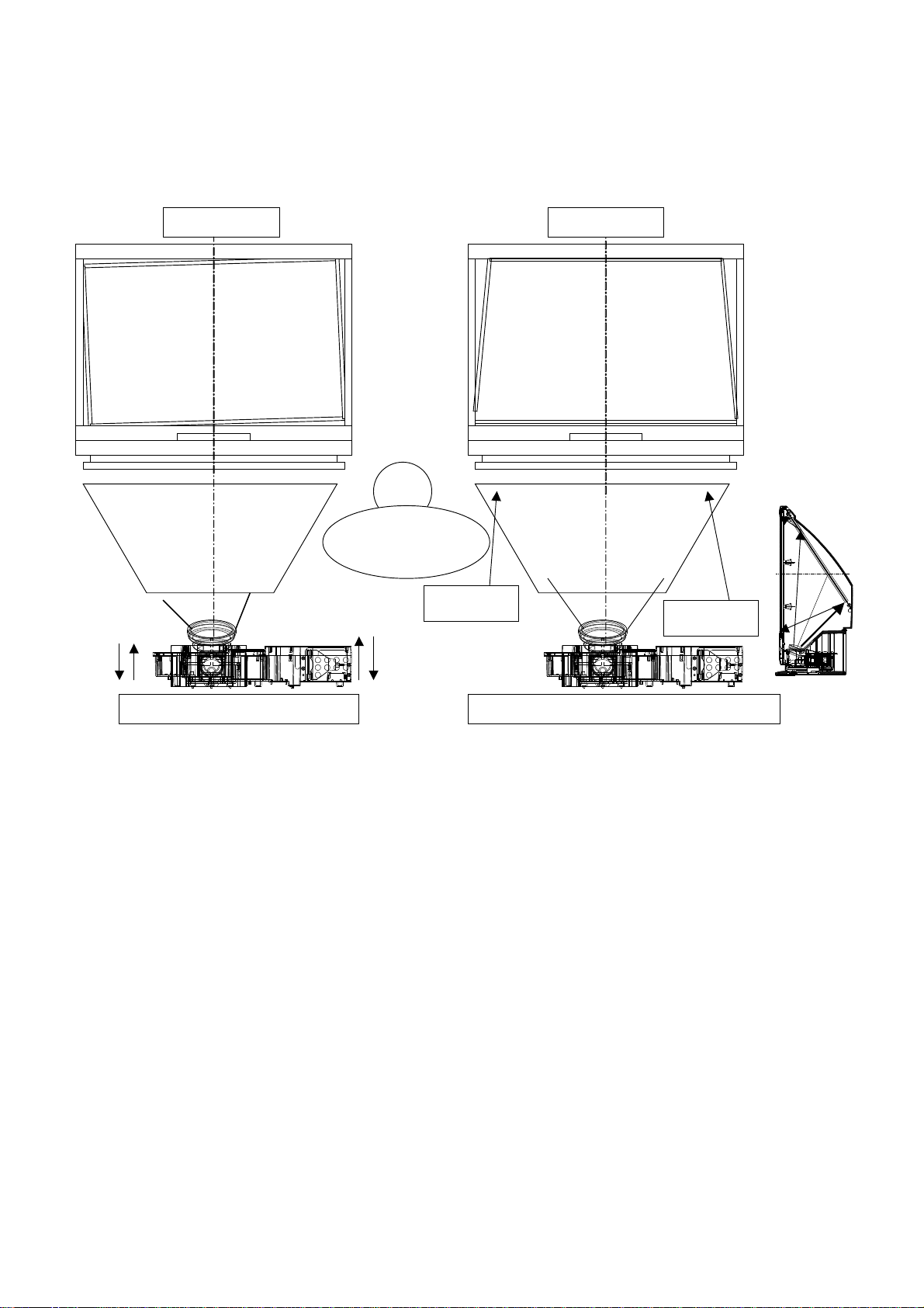
1. Screen Tilt and Keystone cause of occurrence
When the whole engin is leaned, Tilt occur and Keystone occur because of changing TCL
when projection angle of engine is different or Mirror angle is different.
- 13 -
Correction of Screen Tilt & Keystone
TILT-Up and down operation necessity
of the whole engine
Rotation and side angle operation necessity
of the whole engine
KEYSTONE-TLC is
shorter than down
KEYSTONE-TLC is
shorter than down
Mirror angle
Engine projection angle
Comm
-onness
TILT KEYSTONE
Page 14

2. New Mechanism for Adjustment
The axis of rotation of engine sets back and the whole engine enable left and right rotation, up and down, left and right angle
movement.
When turning adjustment Knob of left/right in front, engine will move.
When moving the engine base with left and right direction in front, engine will rotate.
- 14 -
Rota
-tion
Fixing Boss
Adjustment Knob
Adjustment Knob
Locking Knob
engine
engine
supporter
engine base
engine base For calculation : When
projection lens 0.2c leans,
Keystone occurs 5mm.
engine base
The axis of rotation
The axis of rotation
Side angle
Left/Right
angle
pole
Page 15

3. Working Method and Improvement for Correction Mechanism of Tilt and Keystone
3.1 Working Method
(1) Put the 3t spacer on back of down parts of Mirror to correcting the Mirror angle of down parts
- To correct difference between Mirror angle of C/Aand JIG angle of lighting parts.
(2) Looking at the screen, push the engine base for left/right direction in front of engine. At this time,
check the screen Keystone condition.
(3) Adjust engine angle by turning the adjustment Knob on the down part.
(4) If Tilt and Keystone is [MAX-MIN] # 4mm, lock the locking Knob of left/right in front part and then fix
the fixing boss with screw.
3.2 Improvement
When turning left and right rotation, because an engine construction structure is tuched a construction
structure of cabinet, shield case will be correction. When turning adjustment Knob, operation is bad
because you cann’t input a hand to turning or adjustment Knob is tight.
Continously consult with the production department for improving adjustment operation. (A special
Driber for adjustment and so on)
- 15 -
3t spacer
engine base
engine
Fixing Boss
Adjustment Knob Adjustment Knob
Page 16

* Connect your dealer or LG service center for replacing of new lamp.
You must replace the lamp when:
¯ The projector image get darker or start to be deteriorated.
¯ The lamp indicator is red(red, flashing alternately).
¯ The massage “LAMP REPLACE“ appears on the screen when turning the projec-
tor lamp on.
* Replace the lamp as below sequence
1. Turn off the projector and unplug the power cable.
(Cool the lamp for more than 1 hour.)
2. Remove the four retaing screws on the lamp cover with a screwdriver of “+“ type
and then lift off the lamp cover.
3. After lifting the lamp cover off, remove the two retaing screw on lamp case with
screwdriver of “-“ type. (refer to fig.2)
4. Lift up the fixed wire handle of the lamp. (refer to fig.3)
5. Pull out the handle slowly and remove the lamp case.
6. Insert the new lamp gently into the correct position. Make sure it is inserted correctly.
7. Tighten the screw you removed in step 3.
8. Replace the lamp cover and tighten the cover screws.(Make sure the almp cover
is securely fastend. If lamp cover is open, the lamp indicator flashes green and
the projector is not turn on.)
* Resetting the lamp time
After pressing the “?“ key on the remote control in Stand-By mode, press the “9876“
and press the “OK“ button.
And then three LED in the front is stop after flashing for a moment.
* Lamp Life Time Confirmation
1. Method1 : Enter ADJ mode with using the remote control. You can be confirmed
because “ Lamp Life Time XX hr“ is appeared.
2. Method2 : With using the remote control offerd to consumer if you press the
menu button continuously, OSD menus will disappear then press the “9876“ and
press the “OK“ button to enter ADJ mode you can see “Lamp Life Time XX hr“
- 16 -
Replacing the Lamp
< Fig. 1>
< Fig. 2>
< Fig. 3>
Page 17

1. Power Block
Circuit is to use the FLYBACK CONVERTER way for insulation basically and composed of HYBRID IC STR F6658B for
switching power, which has a POWER MOSFET within, and
STR G6153 as the circuit for stand-by. And it is operated by
the ERROR AMP (IC802, SE105) which transfers electric signal in output part to the primary part with insulating primary
and secondary part.
1.1 Block Diagram (STR F6668B)
1.2 Pin Description
1.3 Others
1.4 Function & Description of each terminals
(1) Vin terminal (4 PIN), Start circuit
The Start circuit performs the operation start and stop of control IC by voltage of Vin terminal (4 PIN).
In power start, C2 is charged through the start resistor Rs.
If the Vin terminal voltage reaches 16V (TYP), control IC
starts operating and current increases by the operation of
Start circuit. If this voltage decreases and reaches lower than
10V (TYP), the control IC stops and returns initial states by
the operation of UVLO (operation stop circuit).
The control circuit gains power by rectifying the trans wire
wound D after operation.
As the voltage of trans wire wound doesn’t go up to the set
voltage just after operation, the Vin terminal voltage begins to
decrease. But as the voltage of operation stop is set to 11V
(Max), the voltage of trans wire wound reaches the set value
and control IC keeps operating while the Vin terminal voltage
decreases to the voltage of operation stop.
The Vin Start voltage (Terminal 4) is 16V (TYP), the voltage
of operation stop is 10V (TYP) and the Vovp voltage is 22.5V
(TYP).
(2) OCP / FB terminal (Terminal 1), Oscillator
and Constant voltage control circuit
The oscillator is to use charge or discharge of internal condensor C1 and to select PRC (Pulse Ratio Control) which
fixes off time of MOSFET and changes on time of it.
The voltage regulator Vr4, which is generated when the FB
current through Photo Coupler flows in R4, is approved by
Vr5. Because of this, Comp. 1 reverses and needed voltage
value of Vr5 (peak value of Id) is supplied from Vr4(FB current). Like this Output control is current mode control.
(3) OCP / FB terminal (Terminal 1) and OCP circuit
OCP circuit is the Protection circuit against over-current
which selects the pulse by pulse way. This way is to reverse
oscillator output by detecting peak value of MOSFET drain
current every pulse.
Detecting MOSFET drain current is done by connecting R5
with MOSFET source terminal (Terminal 2) and GND terminal
(Terminal 3) and by inputting regulated voltage to OCP/FB
terminal. The threshold voltage Vth (1) of OCP terminal is
about 0.73V compared with GND. External components R4
and R5 are Filter circuit to protect malfunction by surge current which is generated in MOSFET On.
- 17 -
Description of each Block Circuits
1
2
3
4
5
O.C.P/F.B
S
D
Vin
GND
No.
Symbol Name Function
Input signal of detecting
over-current & to input
signal for controlling constant voltage.
Over-current
/Feed-Back
terminal
MOSFET sourceSource
terminal
MOSFET drainDrain
terminal
Input control circuit powerVoltage input
terminal
GroundGround
terminal
Symbol Function
O.V.P Internal Protect circuit against over-voltage
T.S.D Internal Protect circuit against overheat
Start Circuit Vin terminal voltage waveform
Vcc
5
START
Internal Bias
Reg1 (9.4V)
Reg2 (7.2V)
Reg3 (7.2V)
TSD
Internal Bias
Internal Bias
Counter
OVP
OSC
Mirror
FB Current
Detector
4
FB
Latch
S
R
Q
FB OCP
Drive
Buffer
Amp.
1
D
2
OCP
3
GND
Vcc
5pin)
Internal Bias
Reg.
Icc
15mA(TYP)
13mA(TYP)
70µA(MAX)
20VVcc(ON)Vcc(OFF) 15V
Vcc
Page 18

In light load, if output voltage decreases, the trans wire
wound voltage in primary part also decreases proportionately
and the Vin terminal voltage in primary part reaches lower
than operation stop volate so that OCP circuit stops operating. In this case, the circuit current decreases so that the Vin
terminal voltage increases in proportion to charge current by
start resistance Rs again and intermittent operation occurres
which restarts in operation start voltage.
The advantage of adding the Protection circut against overcurrent is as follows. When input voltage is high, the surge
voltage becomes low by controlling MOSFET drain current
low and stress of voltage in MOSFET becomes less in start
and overload.
And stress of current in secondary Diode can be also less by
controlling output voltage regular.
(4) Latch circuit
Latch circuit is to stop power circuit operating by keeping the
output of oscillator low in operating of two circuits (OVP &
TSD) which protect Over-voltage and overheat.
Latch circuit is to protect malfunction caused by noise etc..
And this circuit starts to function when OVP and TSD operates for more than 8 seconds. In this case, delay time is set
by timer circuit in control IC.
Though Latch circuit operates, Constant voltage power (Reg)
circuit in control IC is also operating and the circuit current is
high. So the Vin terminal voltage decreases rapidly.
If the Vin terminal voltage becomes lower than operation stop
voltage 10V (TYP), circuit current becomes below 400uA and
the Vin terminal voltage begins to increase. On the contrary, if
the Vin terminal voltage reaches operation start voltage 16V
(TYP), circuit current begins to increase and the Vin terminal
voltage begins to decrease.
In other words, the Vin terminal voltage rises and falls
between 10V (TYP) and 16V (TYP).
Like this, the latch circuit protects the Vin terminal voltage
from increasing abnormally.
Releasing latch circuit is done by making the Vin terminal
voltage lower than 6.5V and generally latch circuit is restarted
after cutting AC input.
(5) Protect circuit against overheat
This circuit lets latch circuit operate when the frame temperature of Hybrid IC is above 140°C(Min).
Actual temperature is detected by control circuit element. This
is to protect MOSFET from overheat which is caused by the
system that MOSFET and control circuit element are on the
same frame.
(6) Protect circuit against over-voltage
This circuit lets latch circuit operate when the Vin terminal
voltage exceeds 22.5V (TYP) and this is used to protect the
Vin terminal in control circuit from over-voltage.
Commonly the Vin terminal is supplied with subsidiary wire
wound of Trans and this voltage is in proportion to output
voltage so that this Protect circuit against over-voltage operates in over-voltage output in secondary part when the circuit
of detecing voltage is open.
1.5 STR G6153T(ST-BY STR)
(1) Description of each terminals
Others
(2) Operation stop circuit (UVLO)
This begins operation control if voltage is supplied to low subsidiary current terminal (Vcc) 5PIN.
If the supplied voltage in the same terminal reaches operation
start current voltage (Vcc), 17.5V (TYP), current is supplied to
circuits within IC and then the operation stop circuit (UVLO)
begins operaiton control and high impedence is sustained
until the supplied voltage reaches the same voltage. In this
time, the supplied current is circuit current (Icc) in not operating and it is 70Ua (Max).
If the operation stop circuit begins operation control, circuit
current (Icc) in operation, about 15mA flows in the same terminal. In controlling operation, if the supplied voltage in this
terminal goes below operation stop current voltage (Vcc),
11.5V (TYP), IC stops functioning.
Like this, this terminal plays a roll to detect supplied voltage
and to control operation start in low voltage input.
(3) Internal Oscillator (OSC)
Condernsor to determine oscillation frequency : Ct
If IC begins operating, Ct is charged from internal power by
constant current I1. At this moment, both SW1 and SW2
become open.
If electric potential of charge reaches about 4V, comparator
reverses, and SW1 and SW2 are on simultaneously.
If setting the state that I1 is lower than I2, SW1 becomes on,
Ct gets discharged and Vt decreases.
Oscillation is made by these operations.
Maximum Duty cycle of oscillator is set to 80% (TYP) and frequency is set to 100KHz (TYP). Globular shaped wave output
of Comparator is used as timing clock in internal circuit and
triangle shaped wave output is used as standard signal for
transforming pulse width which will be mentioned later.
- 18 -
1
2
3
4
5
D
OCP
GND
FB
Vcc
No.
Symbol Name Function
MOSFET drainDrain
terminal
Input signal of detecting
over-current in primary
part
Over-current
terminal
Ground
Ground
terminal
Input signal of controlling
constant voltage
Feed-Back
terminal
Input control circuit power
Power
terminal
Symbol Function
OVP Protect circuit against over-voltage
OLP Protect circuit against overload
TSD Protect circuit against overheat
SS Soft start function
Page 19

(4) Control mode (PWM Latch / Feed Back)
Control mode of IC uses MIX Mode which is switched to the
voltage control mode in lightload and and current control
mode in heavyload linearly according to load.
MIX control mode operates PWM control comparing standard
triangle shaped wave with current waveform piled up on DC
FB voltage. So input voltage difference of PWM Comparator
in waveform cross becomes bigger and as a result, stable
PWM signal is gained.
In MIX control mode, enough noise margin can be obtained
with changing voltage PWM of standard triangle shaped
wave. Also,even in continuation inductor mode in which On
Duty is over 50%, Sub-harmonic phenomenon is suppressed
and every essential part of internal oscillator becomes optimum.
(5) Protect circuit, Protect circuit against over-voltage,
Protect circuit against overheat (OLP/OVP/TSD)
1) Protect circuit against overload
This IC has protect circuit against over-current which
detects over-current every pulse.
In over-current, FB system cuts Photo Coupler for FB off
because output voltage doesn’t reach set voltage.
If detecting “Over-current Detector” signal and the “FB
Current Mirror Detector” signal, internal timer count starts
operating 655ms later after detection.
Just after overflow, the “Count Out” signal is output and at
the same time previous operation is stopped. In this state,
main switch is fixed to off and latch circuit starts operating.
Also, in latch operation, latch circuit needs 400uA (Max)
for maintenance and this current is influenced by the electric potential of Vcc terminal.
If the supplied voltage in Vcc terminal goes below power
voltage for releasing latch circuit, 8.7V (TYP), latch operation can be released. When this latch operation is
released, this IC begins start operation from Soft Start.
2) Protect circuit against over-voltage
If the supplied voltage in subsidiary power terminal (Vcc)
of this IC exceedes 22.2V (TYP), oscillation operation is
stopped by the protect circuit against over-voltage, and in
this state, main switch is fixed to off and latch operation
begins.
* power voltage Vcc(ovp) for OVP operation = 22.2V (TYP)
3) Protect circuit against overheat
When the temperature of internal chip reaches 150°C
(TYP), oscillation operation stops. In this state, main
switch is fixed to off and latch operation begins.
(6) Soft Start, Protect circuit against over-current
1) Protect circuit against over-current
In main switch’s on, drain current is monitored. If drain current over standard value is detected, main switch is
switched to off immediately. This drain current detection is
performed every time main switch is on. The standard voltage in OCP terminal is 0.75V (TYP).
2) Soft Start function
Aa this IC has Soft Start function which is Timer way,
external condensor for Soft Start is unnecessary.
Soft Start function is performed by increasing standard
voltage for detecting over-current step by step and by controlling current in main switch.
There are 4 steps and voltage level and continuant time of
each steps are fixed inside. Table SS(1) ~ SS(4) shows
this.
- 19 -
Symbol
Vss(1)
Vss(2)
Vss(3)
Vss(4)
MIN
0.16
0.35
0.51
0.63
TYP
- -
- -
- -
- -
MAX
0.35
0.54
0.68
0.75
Page 20

2 MSP3410G : Sound Block
(1) Introduction
The MSP 3410G family of single-chip Multistandard Sound
Processors covers the sound processing of all analog TVStandards worldwide. The full TV sound processing, starting
with analog sound IF signal-in, down to pro-cessed analog
AF-out, is performed on a single chip.
Figure shows a simplified functional block diagram of the
MSP 3410G.
Surround sound can be reproduced to a certain extent with
two loudspeakers.
These TV sound processing ICs include versions for processing the multichannel television sound (MTS) signal conforming to the standard recommended by the Broadcast
Television Systems Committee (BTSC).
The DBX noise reduction, or alternatively, MICRONAS Noise
Reduction (MNR) is performed alignment free.
The MSP 3410G has built-in automatic functions: The IC is
able to detect the actual sound standard automat-ically
(Automatic Standard Detection). Furthermore, pilot levels and
identification signals can be evaluated internally with subsequent switching between mono/stereo/bilingual; no I
2
C inter-
action is necessary (Auto-matic Sound Selection).
(Fig Simplified functional block diagram of the MSP 3410G)
(2) Features
• Automatic Standard Detection of terrestrial TV standards
• All NICAM standards
• All Analog FM-Srereo A2 standards
• Simultaneous demodulation of high-deviation FM-Mono and
NICAM (China)
• Very high-deviation FM-Mono mode(China,Eutelast,etc.)
• FM demodulation of all analog satellite standards.
• ADAPTIVE deemphasis for satellite(According to ASTRA
specification)
• ASTRADigital Radio(ADR) together with DRP3510A.
(3) Sound IF Processing
1) Analog Sound IF Input
The input pins ANA_IN1+, ANA_IN2+, and ANA_IN-offer
the possibility to connect two different sound IF(SIF)
sources to the MSP 3440G. The analog-to-digital conversion of the preselected sound IF signal is done by an A/Dconverter. An analog automatic gain circuit(AGC) allows a
wide range of input levels. The high-pass filters formed by
the coupling capacitors at pins ANA_IN1+ and ANA_IN2+.
2) Demodulator: Standards and Features
The MSP 3440G is able to demodulate all TV-sound standards worldwide including the digital NICAM system.
Very high deviation FM-Mono: Detection and robust
demodulation of one FM carrier with a maximum devi-ation
of 540 kHz.
- 20 -
Page 21

(3) Block Diagram
- 21 -
Fig Signal flow block diagram of the MSP 3410G(input and output names correspond to pin names)
Page 22

3. LCD Driver Part
3.1 E07050K0A : Video Signal Processor IC for TFT-LCD
(1) Scope
These specifications apply to the E07050K0A CMOS IC.
<Feature>
1) Operation clock frequency Max. 85 MHz
2) RGB swap function (RGB three-system set's video signals can be swapped via external settings)
3) Contrast and brightness adjustment functions
4) Ten-bit digital gamma correction function (look-up table type with interpolation process)
5) Image quality improvement function
(Vertical stripes correction, ghost image correction, horizontal crosstalk correction)
6) Built-in OSD function (2 bits • 3 systems, 1 control pin)
7) Output masking of video signals is enabled
8) Color uniformity correction function (look-up table type with interpolation process)
Enables setting of correction data for three brightness levels or four brightness levels.
Two types of screen correction segments (32 horizontal segments • 24 vertical segments or 16
horizontal segments • 12 vertical segments).
9) Enables insertion of reference signal in video signal.
10) Outputs drive signal for panel
11) Data is set via three-wire serial interface
12) Built-in boundary scan function
13) 176-pin (24 mm • 24 mm) QFP package
(2) Block Diagram
- 22 -
rect
ROUT(9:0)
GOUT(9:0)
BOUT(9:0)
HPLL
HRESETO
VRESETO
ENBY1 - 2
DXOUT(R:G:B)
ENBX3(R:G:B)
ENBX4(R:G:B)
ENBX1(R:G:B)
ENBX2(R:G:B)
DYOUT
CLXOUT(R:G:B)
CLYOUT
FRP(R:G:B)
SHCLK(R:G:B)
XFR(R:G:B)
STSQE(R:G:B)
STSQO(R:G:B)
NRG
CLP 1~2
10bit
RIN[9:0]
Reference
voltage
Color
Uniformit y
correct
correct
Picture
quality
V. line cor
H. crosstalk
Ghost
Video
mask
Gamma
cor-
Contrast
Bright
OSD
10bit
10bit
BIN[9:0]
GIN[9:0]
OSDBIN[1:0]
OSDRIN[1:0]
OSDGIN[1:0]
OSDSW
Timing
generator
Range of Video p rocessingUnitdescribed in Chapter8.
Serial
interface
SCS
SCLK
SDATA
HSYNC
VSYNC
DCLK
SELECT
Page 23

3-2 E06070D0A : Video signal conversion IC
for TFT-LCD
(1) Scope
The E06070D0A provides a fast, 10bit latched decimating
digital input, which drives 6
channel high voltage drive outputs. Flexible digital input formats, allow several
L3E06070D0As to be used in parallel for higher resolution
displays.
<Feature>
(1) Operation clock frequency :85 MHz
(2) 10-bit digital video signal input
(3) Digital serial parallel conversion (6-ch output)
(4) Built-in D/A converter (10 bit)
(5) Built-in amplifier for video signal polarity inversion
(6) High slew rate output: Typ. 265 V/µs (can drive a TFT
panel directly)
(7) Wide output dynamic range of 1.5 to 13.5 V
(8) Built-in function for switching scan direction
(9) Low power consumption
(10) 48-pin (7x7 mm 2 ) QFP package
(2) Pin Layout
(3) Block Diagram
- 23 -
DB0
DB1
DB2
DB3
DB4
DB5
DB6
DB7
DB8
DB9(MSB)
CLK
47
48
1
2
3
4
5
6
7
8
9
10
11
12
141516171819202122
13
E/O
XFR
46
R/L
STSQ
45
INV
DGND
43
44
DVCC
AVCC(DAC
41
42
VREF
AGND(DAC
40
BYP
STBY
VMID
VMID
38
39
23
AGND1
37
36
35
34
33
32
31
30
29
28
27
26
25
24
VID1
AVCC1,2
VID2
AGND2,3
VID3
AVCC3,4
VID4
AGND4,5
VID5
AVCC5,6
VID6
AGND6
CLK
STSQ
XFR
E/O
R/L
STBY
BYP
VREF
VMID
10
CHANNEL
SELECTOR
BIAS
SCALING
CONTROL
DB[0:9]
2-Stage
Latch
10 10
2-Stage
Latch
10 10
2-Stage
Latch
10 10
2-Stage
Latch
10 10
2-Stage
Latch
10 10
2-Stage
Latch
1010
DAC
DAC
DAC
DAC
DAC
DAC
VMIDINV
VID1
VID2
VID3
VID4
VID5
VID6
AGND(BIAS)
AVCC(BIAS)
Page 24

3.3 E01031F0A : TFT-LCD Level Shifter IC
(1) Scope
The L3E01031F0A is an interface IC for driving TFT active
matrix panels with built-in drivers. Its high
voltage circuit acts as an interface between the control IC
and the drivers on the LCD panel.
<Feature>
(1) Clock Frequency Max. 4.2 MHz
(Care is required to avoid exceeding the allowable power
dissipation for the package, which is 280mW.)
(2) Internal level shift circuit converts input to a signal capable
of driving a TFT panel.
(3) Built-in multiplex function to switch the panel auxiliary signal.
(4) CMOS Si-Gate process.
(5) 48-pin plastic flat package (lead pitch 0.5mm QFP).
(6) Does not feature radiation resistant or light and noise
resistant design.
(2) Pin Layout
- 24 -
(3) Block Diagram
Page 25

- 25 -
DESCRIPTION OF MICOM
1. Feature of MICOM Function
1-1. Signal Selection
(1) Input signal selection : RGB1(Analog)/RGB2(Analog)/RGB3(Analog/Digital)/Video/S-Video/Component
(2) A/V color standard automatic signal selection : NTSC/PAL/SECAM/NTSC 4.43/PAL M/PAL N/PAL 60
-> Automatic system detection
(3) Specification of PC input signal : Refer to “PC Input Specification Table”.
(4) Specification of Component input signal : 480I,480P,DVD 625Line,576P,720P,1080I 50Hz,1080I 60Hz
1-2. Video Interpolation Extension, Compression Support
You can control the correspondent IC like scaler after discrimination of input signal. If the resolution is lower than
XGA, you can extend it to the XGA scale. Or if it is higher than XGA, you can compress it to XGA scale.
* Resolution : Set the resolution lower than 1280x720 in order to adjust the picture of panel (resolution:1280x720) to the screen.
1-3. Judging No Signal
OSD,SOUND Mute
1-4. Video Signal Adjustment
(1) Analog RGB(PC) input : Contrast, Brightness, Color(R, G, B)
Clock, Phase, H Position, V Position
(2) Digital RGB (DVI) input : Contrast, Brightness, Colorr(R, G, B)
Clock, Phase, etc. are automatically adjusted on auto tracking mode, but noise can be included in the signal
owing to the IC specification and also they can’t be adjusted precisely according to the signal pattern.
So the manual to adjust Clock, phase, etc. manually.
1-5. Sound Signal Adjustment
Volume, Mute,DASP,AVL,MIC
1-6. Other Functions
Item
ARC(Aspect Ratio Control)
ZOOM
Checking Lamp Time
OSD Language Selection
Auto Tracking
Set ID
APC(Auto Picture Control)
Audio Input
Analog/Digital RGB :4:3,16:9 mode Toggle funtion
Video/S-Video/Component :4:3,16:9 ,zoom 1,zoom 2,zoom 3 mode Toggle funtion
Adjusting the magnification of zoom by shortened key.(+/- 25 level)
Checks used time to now and displayes the fact when replacing time gets.
Korean, English, French, German, Italian, Spanish, Chinese,Japanese
Automatically controlling CLOCK, PHASE
Characteristic number of set which is used to adjust the funtions of set with PC by
connecting RS-232C terminal(1~99).
When the Set ID specified in PC P/G accords with the set ID specified in the
set,the funtions of set can be controlled by using the menu of PC P/G.
By using this menu,you can select “clear”,”soft”,”comfortable” or “off” in Video,SVideo,Component.
By using this menu,make speaker output by selecting audio input R/L or Mic.
And you can use R/L by connecting the stereo output from DVDP or STB.
REF
1-7. Controlling Power
(1) ST-BY -> Power On key in -> Main Power On -> Fan Off -> Blue Background -> Lamp On
-> LOGO ON -> Video output or No signal
(2) Power Off key in -> Lamp Off -> Audio mute -> Fan Off -> Main Power Off -> ST-BY
1-8. Data Saving
EEPROM(24C256), EEPROM IIC BUS
Page 26

- 26 -
1-9. Warning OSD and Controlling LED
Operation indicator LED Orange 7 Stand-By
Orange(flashing)
Green 7 Run
Green(flashing)
Off
Lamp Indicator LED Red
Red(flashing)
Green(flashing)
Temperature indicator Red
LED Red(flashing)
Green(flashing)
7 lamp is cooling as power out(1 minutes),Ignore the power on input.
7 7 Sec. : Cooled for a minute before turning off the lamp.
7 25 Sec. : Didn’t cool the lamp for a minute while turning off the lamp.
7 Off (the state that AC S/W is off or the Power cable isn’t connected)
7 Warning the life of lamp, Needing to replace the lamp ( over 10000H)
7 Displaying OSD for lamp warning when power on.
7 Lamp on error. ( case of lamp isn’t on when power on )
7 Turn on the lamp and start the detect after 5 seconds.
When occuring error,turn off the lamp at once.
7 Warning of lamp case open
7 Power off forcedly, Not Power on
7 High temperature.Power off
7 Warning of fan1 malfunction. (Perceived after 20 ~ 60 seconds because it takes a
little time to check internally. )
7 Warning of fan2 malfunction. (Perceived after 20 ~ 60 seconds because it takes a
little time to check internally. )
1-10. Checking and Initiating the Lamp Time
Used lamp time is displayed on the menu.
(1) Over 10000 hours : Informs warning.(Red LED), Displaying warning OSD when power on.
If you don’t initializing the lamp,it is always display warning OSD on screen when turning on the lamp.
(2) Initiation : Used time must be initiated by the user after replacing the lamp.
You can move to the next service menu by pressing the “MENU” key,and when you press the “MENU” key
continuously,you can move to “LAMP TIME RESET” menu.
If you press the “+” key (VOL+) in this menu,the user lamp time is reset.And then press the “ENTER” key to come out
of service menu.
Caution : Changing the set value in other menus besides “LAMP TIME RESET” or input other keys besides “MENU” key can cause
serious problem to the lamp.Always use the “ENTER” key to cancel the service menu in “LAMP TIME RESET” menu.
1-11. Remote Mouse Control
(1) Funtion the mouse of PC.
(2) Apply the 16 directions and left,right click/drag.
(3) Apply the function of the PS/2,MAC Mouse.
1-12. DDC1/2B
Use the specified IC-24LC21 for DDC1/2B to write EDID table data on 24C21 through adjustment Zig.
Page 27

- 27 -
1-13. Micom Controlled IC’s
Chip Name
24LC256
MSM82C55
PW164
VPC3230D
FLI2200
ET7050
M62320
AD9884
M62352
AT24LC21
EEPROM
PORT EXPANSION IC
MICOM EMBEDDED
SCALER IC
VIDEO DECODER
VIDEO DEINTERLACE IC
TIMING GENERATOR
GAMMA/COLOR UNIFORMITY
I2C Controlled OUTPUT PORT
ADC
DA CONVERTER
DDC 1/2B
1-14. PC Input Specification Table
O HD sigal(D-Sub 15pin input)
(1) 280X720,60Hz/59.94Hz
(2) 1920X1080,Interface 60Hz/59.94Hz
Function
VGAEGA
PC98
(VGA Text)
VGA
Resolution
640 x 350
640 x 350
640 x 400
720 x 400
720 x 400
640 x 480
640 x 480
640 x 480
640 x 480
640 x 480
Vertical Frequency
70.090Hz
85.080Hz
85.080Hz
70.082Hz
85.039Hz
59.940Hz
72.800Hz
75.00Hz
85.008Hz
100.040Hz
Horizontal Frequency
31.468KHz
37.861KHz
37.861KHz
31.469KHz
37.927KHz
31.469KHz
37.861KHz
37.500KHz
43.269KHz
53.011KHz
Page 28

- 28 -
Resolution
Vertical Frequency
Horizontal Frequency
SVGA
XGA
SXGA
800 x 600
800 x 600
800 x 600
800 x 600
800 x 600
800 x 600
1024 x 768
1024 x 768
1024 x 768
1024 x 768
1024 x 768
1152 x 864
1152 x 864
1152 x 864
1152 x 864 *
56.250Hz
60.317Hz
72.188Hz
75.00Hz
85.061Hz
100.00Hz
43.479Hz
60.004Hz
70.069Hz
75.029Hz
84.997Hz
60.053Hz
70.016Hz
75.00Hz
85.057Hz
35.156KHz
37.879KHz
48.077KHz
46.875KHz
53.674KHz
64.016KHz
35.522KHz
48.363KHz
56.476KHz
60.023KHz
68.677KHz
54.348KHz
63.995KHz
67.500KHz
77.487KHz
1280 x 960
1280 x 960
1280 x 1024
MAC
HD
“*” : Only available to RGB1,2 mode.Not applied to RGB3 mode.
16¡–
19¡–
21¡–
1024 x 768
1024 x 768
1152 x 870
1920 x 1080i *
1280 x 720 *
1-15. AV Input Specification
Item
Video Input applicable
System
832 x 624
Specification
NTSC M
NTSC 4.43
PAL B,G,H,I
PAL M
PAL N
SECAM
PAL 60
60.00Hz
75.00Hz
60.020Hz
74.550Hz
60.004Hz
75.029Hz
75.062Hz
60.00Hz
60.00Hz
3.579545 / 60 Hz
4.433618 / 60 Hz
4.433618 / 50 Hz
3.575611 / 60 Hz
3.582056 / 50 Hz
4.286 / 50 Hz
4.433618 / 60 Hz
60.00KHz
75.00KHz
63.981KHz
49.725KHz
48.363KHz
60.023KHz
68.681KHz
33.750KHz
45.00KHz
Remark
Page 29

- 29 -
1-16. S-VIDEO Input Specification
: NTSC/PAL
Item
Video Input applicable
System
Specification
NTSC M
PAL B,G,H,I
3.579545 / 60 Hz
4.433618 / 50 Hz
1-17. Component(DVD/HD STB) Input Specification
Specification
No.
Resolution
1
2
3
4
5
6
7
8
640 x 480
640 x 480
704 x 480
720 x 576
720 x 576
1280 x 720
1280 x 720
1920 x 1080
H-Freq(KHz)
15.73
15.63
31.47
15.625
31.25
45.00
44.96
31.25
V-Freq(KHz)
60
59.94
59.94
50.00
50.00
60.00
59.94
50.00
Remark
Proposed
SDTV,DVD 480I
SDTV,DVD 480I
EDTV 480P
SD 576I(625 Line)
HDTV 576P
HDTV 720P
HDTV 720P
HDTV 1080 50I
10
9
1920 x 1080
1920 x 1080
33.75
33.72
60.00
59.94
HDTV 1080 60I
HDTV 1080 59.94I
Page 30

- 30 -
2. Block Diagram
IRRCVR0
IRRCVR1
PORTA0
PORTA1
PORTA2
PORTA3
PORTA4
PORTA5
PORTA6
PORTA7
EXTINT0
PW164
8255A
Parallel
Controller
EEPROM
24LC256
A2~A1
D15~D0
WE
RD
PORTB0
PORTB1
PORTB2
PORTB3
PORTB4
PORTB5
PORTB6
PORTB7
CS0
CS1
VPC3230D
FLI2200(Faroudja)
ET7050
M62352
1 st
CS
A1~A0
D7~D0
WE
RD
CS
PC
0
PC1
PC2
PC3
PC4
PC5
PC6
PC7
PA0
PA1
PA2
PA3
PA4
PA5
PA6
PA7
PB0
PB1
PB2
PB3
PB4
PB5
PB6
PB7
P11
P12
P13
P14
P15
P16
VREF
VMID
RLCCOM
RNRSH
RNRSL
GLCCOM
GNRSH
GNRSL
BLCCOM
BNRSH
BNRSL
N.C
P1
7
P18
P19
P110
P111
P112
KEY_OUT1
KEY_OUT2
KEY_OUT3
SDAT
SCLK
ET7050_CSEL
M62352_CS
M62352_CS2
SCDT
N.C
TEMP_DET
LAMP_ON_DET
CASE_DET
PC_SEL2
WP
N.C
SDA
SCL
N.C
E_SDA
E_SCL
SDA_2
SCL_2
N.C
N.C
M62352
2nd
CS
P2
1
P22
P23
P24
P25
P26
N.C
MOUSE_RESET
UDI
LRI
COR_CON
N.C
N.C
MUTE
N.C
TEMP_REF
N.C
N.C
P2
7
P28
P29
P210
P211
P212
3503_CS
62352_CS1
SDAT5
SCLK5
N.C.
CASE_DET
POWER_KEY
LAMP_DET
FAN2-DET
KEY_IN1
V_480IP_DET
LAMP_DET
KEY_IN2
FAN_DET
N.C
KEY_IN3
2
16 8
M62320
(LED Control)
Page 31

- 31 -
2-1. Description of Control Part
No.
A19~A0
D15~D0
/RD
/WE
IRRCVR0
IRRCVR1
PORTA0
PORTA1
PORTA2
PORTA3
PORTA4
PORTA5
PORTA6
PORTA7
PORTB0
PORTB1
PORTB2
PORTB3
PORTB4
PORTB5
PORTB6
PORTB7
CS0
CS1
EXTINT0
EXTINT1
PA
0
PA1
PA2
PA3
PA4
PA5
PA6
PA7
PB0
PB1
PB2
PB3
PB4
PB5
Symbol I/O Active Reset Function
IRRCVR0
IRRCVR1
SDA
SCL
NC
E_SDA
E_SCL
SDA_2
SCL_2
N.C
SCDT
N.C
TEMP_DET
LAMP_ON_DET
CASE_DET
PC_SEL2
WP
N.C
8255_CS
N.C
N.C
N.C
N.C
LAMP_ON
FAN_ON
POWER_ON
PC-VIDEO-SEL
PC_SEL1
ADDOWN
TMDSOE
FAN2_DET
KEY_IN1
V_480IP_DET
LAMP_DET
KEY_IN2
FAN_DET
O
I/O
O
O
O
O
I/O
O
O
O
O
I/O
I/O
O
I/O
I/O
O
I/O
I/O
I/O
I/O
O
O
O
O
O
O
O
L
L
I
I
H/L
H/L
H/L
H/L
H/L
H/L
H/L
H/L
H
I
H/L
H
I
H
I
H
I
H/L
H/L
H/L
L
H
H/L
H/L
H/L
H/L
H
H
L
L
L
H
L
H
I
I
I
I
I
I
7 Address Bus
7 Data Bus
7 Read Enable
7 Write Enable
7 Remote Control IR Signal : IR is NEC Format
Not Used
2
7 I
C Bus Clock & Data Line
7 AD9884, FLI2200, VPC3230D, CXA2101
Not Used
7 EEPROM I
7 EEPROM I
7 LED Control I
7 LED Control I
2
C Bus Data Line (EEPROM,24LC256)
2
C Bus Clock Line (EEPROM,24LC256)
2
C Bus Data Line (M62320)
2
C Bus Clock Line (M62320)
Not Connection
7 Sync detection from TFP401.
Not Connection
7 Temperature detect
7 Lamp On/Off status detect.
7 Lamp case open error detect.
7 Selection between RGB3 and RGB1,2 selection result.
7 EEPROM(24LC256)Write protection
Not Connection
7 MSM82C55A Chip Select(for IC Control using data bus)
Not Connection
Not Connection
Not Connection
Not Connection
7 Lamp ON/OFF (HIGH/LOW)
7 Fan ON/OFF (HIGH/LOW)
7 Main Power ON/OFF (HIGH/LOW)
7 Select PC or AV(From CXA1201) for AD9884 input.
7 Select between RGB1 or RGB2.
7 ADC(AD9884) power down for digital RGB3.
7 TFP401 digital RGB output enable for digital RGB3.
7 Fan2 operation error detect(High:fan error)
7 Inputs for KEY Scanning
7
Detect component input(480i or higher resolution->low:480i)
7 Lamp on/off status detect.(High:lamp error)
7 Inputs for KEY Scanning
7 FAN1 operation error detect.
Page 32

- 32 -
No.
Symbol I/O Active Reset Function
PB
PB7
PC0
PC1
PC2
PC3
PC4
PC5
PC6
PC7
P11
P12
P13
P14
P15
P16
P17
P18
P19
P110
P111
P112
P21
P22
P23
P24
P25
P26
P27
P28
P29
P210
P211
P212
PL0
PL1
PL2
PL3
PL4
PL5
PL6
PL7
6
N.C.
KEY_IN3
KEY_OUT1
KEY_OUT2
KEY_OUT3
SDAT
SCLK
ET7050-CSEL
M62352_CS
M62352_CS2
VREF
VMID
RLCCOM
RNRSH
RNRSL
GLCCOM
GNRSH
GNRSL
BLCCOM
BNRSH
BNRSL
N.C.
I
I
H/L
O
H/L
O
H/L
O
H/L
O
H/L
O
H/L
O
H/L
O
H/L
O
Analog
O
Analog
O
Analog
O
Analog
O
Analog
O
Analog
O
Analog
O
Analog
O
Analog
O
Analog
O
Analog
O
Analog
O
N.C.
N.C.
H/L
MOUSE_RESET
UDI
LRI
COR_CON
O
H/L
O
H/L
O
H
O
N.C.
N.C.
MUTE
O
N.C.
Analog
TEMP_REF
O
N.C
H/L
LAMP_LED1
LAMP_LED2
TEMP_LED1
TEMP_LED2
OPER_LED1
OPER_LED2
O
H/L
O
H/L
O
H/L
O
H/L
O
H/L
O
N.C
N.C
No connection
7 Inputs for KEY Scanning
7 KEYPAD polling output 1
7 KEYPAD polling output 2
7 KEYPAD polling output 3
7 ET7050,M62352 data line
7 ET7050,M62352 clock line
7 ET7050 chip selection (enable) line
7 M62352 selection (enable) line
7 M62352 selection (enable) line
7 Full-scale setting voltage
7 Center video signal setting voltage
7 Potential of opposing electrode of liquid crystal panel(red)
7 TFT panel auxiliary signal input A(red)
7 TFT panel auxiliary signal input B(red)
7
Potential of opposing electrode of liquid crystal panel(green)
7 TFT panel auxiliary signal input A(green)
7 TFT panel auxiliary signal input B(green)
7
Potential of opposing electrode of liquid crystal panel(blue)
7 TFT panel auxiliary signal input A(
7 TFT panel auxiliary signal input B(
blue
blue
)
)
No connection
No connection
No connection
7 Mouse IC(AT89C51) reset signal out
7 TFT panel Y direction select
7 TFT panel X direction select/scan direction switch
7 Uniformity on/off
No connection
No connection
7 Sound IC mute port on
No connection
7
Reference voltage for high temperature detect of thermist.
No connection
7 Lamp indicator
7 Temp indicator
7 Operating indicator
No connection
No connection
Page 33

Block Diagram
- 33 -
Page 34

EXPLODED VIEW
- 34 -
301
121
305
430
640
300
650
310
410
420
520
123
122
120
600
630
303
620
610
501
550
560
530
570
503
580
540
502
174
306
307
302
304
330
660
125
124
590
Page 35

EXPLODED VIEW PARTS LIST
- 35 -
120 120-D38E SPEAKER,MID-RANGE LG FOSTER 8 OHM 15/25W 87DB 12
121 6400VG0001B SPEAKER,TWEETER NO FOSTER 8 OHM 20W/30W XX D77
122 3110V00123A CASE,SPEAKER BOX LEFT
123 3550V00159A COVER,SPEAKER BOX LEFT
124 3110V00124A CASE,SPEAKER BOX RIGHT
125 3550V00160A COVER,SPEAKER BOX RIGHT
174 174-222P POWER CORD ASSY,SAA L=2200MM 219A(305-002H)
300 3091V00328C CABINET ASSY,MW-60SZ12 3090V00259 LG NO .
301 3790V00280A WINDOW FILTER 60” LCD PJTV ACR
302 3350V00015A SCREEN 60”W LCD PJTV.AS,IMPROVED .
303 3211V00047B FRAME ASSY 3210V00074B.BASE U
304 3211V00048E FRAME ASSY BASE MW-60SZ12 LOWER
305 3508V00226E DECORATION,FRONT AL ANODIZING MW-60SZ12
306 3508V00244E DECORATION,FRONT ABS SPRAY MW-60SZ12
307 3508V00228E DECORATION,FRONT AL ANODIZING MW-60SZ12
310 4870V00004E DRAWER
330 5020V00490A BUTTON
410 3809V00252C BACK COVER ASSY,UPPER, 3808V00225A
420 3809V00253C BACK COVER ASSY,LOWER, 3808V00226A
430 5018V00025C MIRROR ASSY,MIRROR
501 3210V00072B FRAME,CHASSIS(DIGITAL)
502 3210V00073A FRAME,CHASSIS(SMPS)
503 4811V00027A BRACKET ASSY,BOARD A/V
520 6871VMMB77A PWB ASSY,MAIN RE-01JB MAIN PCB ASSY
530 6871VPMA02A PWB ASSY,POWER SMPS RE-01JB
540 6871VPMA03A PWB ASSY,POWER SMPS RE-01JB ST-BY
550 6871VSMD42A PWB ASSY,S/AMP RE-01JB SOUND B/D ASSY
560 6871VSMD43A PWB ASSY,A/V RE-01JB ASSY
570 6871VSMD45A PWB ASSY,DIGIT RE-01JB DVI B/D ASSY
580 6871VSMD44A PWB ASSY,RGB RE-01JB PC B/D ASSY
590 6871VSMD54A PWB ASSY,INTER RE-01JB BALLAST
600 3141VSN200B CHASSIS ASSY,ILLUMINATION+COMBIN
610 3110V00139A CASE ASSY,LAMP RN-60SZ10 . .
620 4980V00284A SUPPORTER ASSY,DC FAN . RN-60SZ10
630 6913V00002A LAMP ASSEMBLY,EUC-100L/100V PHILIPS FOR LAMP
640 6871VSN198B PWB ASSY,P/AMP RE01JB ASSY WITH EMI COR
650 6871VSN200A PWB ASSY,INTER RE-01JB INTERFACE B/D AS
660 6871VSN199A PWB ASSY,PSW RE-01JB ASSY
NO.
PART NO.
DESCRIPTION
Page 36

- 36 -
REPLACEMENT PARTS LIST
LOCA. NO PART NO DESCRIPTION
IC1810
IC1870
IC1871
IC2001
IC2003
IC2005
IC2006
IC2101
IC2103
IC2105
IC2110
IC2120
IC2129
IC2130
IC2180
IC2201
IC2203
IC2205
IC2210
IC2220
IC2301
IC2303
IC2305
IC2310
IC2320
IC3002
IC3005
IC3006
IC3200
IC3201
IC3202
IC3203
IC3204
IC3206
IC3210
IC3280
IC3301
IC3302
IC3361
IC3501
D650
D651
D801
D810
D820
D821
D822
D832
D833
D834
D841
0IMCRKE004A
0IMCRSH001A
0IPH740400G
0IMCRSB010A
0IKE702700D
0IMCRKE008A
0ISJ111725A
0IMCRSB008A
0IMCRET001A
0IMO324000C
0IMCRSB009A
0IMCRSB009A
0IMCRSH001A
0IMCRKE008A
0IPRPSH001A
0IMCRSB008A
0IMCRET001A
0IMO324000C
0IMCRSB009A
0IMCRSB009A
0IMCRSB008A
0IMCRET001A
0IMO324000C
0IMCRSB009A
0IMCRSB009A
0ISA715100D
0ISJ111733A
0IFA741230A
0IAL242110A
0IRH765700B
0IRH765700B
0IAD802300A
0IPH740400G
0IAL242110A
0IMCRPH018A
0IAL895112B
0IMCRMN002A
0IFA754207A
0IKE455800E
0IMI623200B
0DD247109AA
0DD247109AA
0DD606000AA
0DD100009AM
0DD100009AM
0DD100009AM
0DD100009AM
0DR010009AA
0DD100009AM
0DD260000BB
0DD120000BB
IC,KIA7427F, KEC SOT89-3P R/TP HI
IC,PQ05DZ1U SHARP 5, SMD TYPE R/T
IC,74HC04D HEX INVERTER 14P,SOP T
IC,L3E07050K0A SEIKO EPSON 176QFP
IC,KIA7027AF 3, SOT-89 TP RESET I
IC,KIA78D33F KEC 3P DPAK R/TP 3.3
IC,EZ1117ACST-2.5 3P SOT ST REGUL
IC,L3E01031F0A SEIKO EPSON 48QFP
IC,EL2244CS ELANTEC 8P SO R/TP VI
IC,LM324D SO-14 TP OP AMP
IC,L3E06070D0A SEIKO EPSON 48QFP
IC,L3E06070D0A SEIKO EPSON 48QFP
IC,PQ05DZ1U SHARP 5, SMD TYPE R/T
IC,KIA78D33F KEC 3P DPAK R/TP 3.3
IC,PQ20WZ1U SHARP 5P SC63 R/TP LO
IC,L3E01031F0A SEIKO EPSON 48QFP
IC,EL2244CS ELANTEC 8P SO R/TP VI
IC,LM324D SO-14 TP OP AMP
IC,L3E06070D0A SEIKO EPSON 48QFP
IC,L3E06070D0A SEIKO EPSON 48QFP
IC,L3E01031F0A SEIKO EPSON 48QFP
IC,EL2244CS ELANTEC 8P SO R/TP VI
IC,LM324D SO-14 TP OP AMP
IC,L3E06070D0A SEIKO EPSON 48QFP
IC,L3E06070D0A SEIKO EPSON 48QFP
IC,LA7151M 10SOP R/TP AUDIO SW FD
IC,EZ1117CST-3.3 3P,SOT-223 TP 3.
IC,DM74LS123MX 16SOP TP DUAL RETR
IC,AT24C21-10SI-2.5 8P,SOP TP 1K
IC,BA7657F 24P,SOP TP INPUT SIG.
IC,BA7657F 24P,SOP TP INPUT SIG.
IC,AD8023AR 14P,SOP TP TRIPLE VID
IC,74HC04D HEX INVERTER 14P,SOP T
IC,AT24C21-10SI-2.5 8P,SOP TP 1K
IC,74LVC126AD PHILIPS 14P SO R/TP
IC,COPY AT89C51-24AC 40PIN TQFO T
IC,MSP3400G QA B6 MICRONAS 80 QFP
IC,KA75420ZTA(KA7542ZTA) 3P,TO-92
IC,KIA4558 8DIP DUAL OP AMP
IC,M62320FP,I/O EXPANDER 16P SOP
DIODE,DETACTOR 1S2471DETECT SW TP
DIODE,DETACTOR 1S2471DETECT SW TP
DIODE,RECTIFIERS RBV606 NA 600V 6A 1
DIODE,RECTIFIERS EU1ZV(1) TP SANKEN
DIODE,RECTIFIERS EU1ZV(1) TP SANKEN
DIODE,RECTIFIERS EU1ZV(1) TP SANKEN
DIODE,RECTIFIERS EU1ZV(1) TP SANKEN
DIODE,RECTIFIERS EG01C TP 1000V 0.5A 1
DIODE,RECTIFIERS EU1ZV(1) TP SANKEN
DIODE,RECTIFIERS BRIDGE D2SBA60(STK)
DIODE,RECTIFIERS FML-G12S
LOCA. NO PART NO DESCRIPTION
IC801B
IC802B
IC604
IC703
IC708
IC811
IC820
IC831
IC832
IC841
IC845
IC851
IC1001
IC1003
IC1004
IC1101
IC1102
IC1103
IC1104
IC1106
IC1108
IC1109
IC1110
IC1201
IC1202
IC1203
IC1504
IC1507
IC1530
IC1600
IC1601
IC1602
IC1603
IC1604
IC1650
IC1660
IC1665
IC1700
IC1704
IC1705
IC1706
IC1707
IC1708
IC1709
IC1710
IC1800
IC1802
IC1803
IC1805
IC1806
IC1808
0ISH817300B
0ISH817300B
0ISA428200A
0ISH052100C
0ISH092100B
0IMCRON002A
0ISK666813A
0ISK615311B
0ISH817300B
0ISH817300B
0ISH122100B
0IMO257633A
0IIT323000C
0IKE704200J
0ISJ111733A
0ISS464323A
0IMCRG2001A
0IMCRAD001A
0IPH740800F
0ISJ111733A
0ISJ111725A
0IKE702700D
0ISJ111733A
0IMCRFA010A
0ISO210100B
0IMCRAT003A
0IRH765700B
0IMCRSH001A
0IDS232000A
0IAD988414A
0IMCRPH018A
0IPRPTI001A
0IPH747400F
0IMCRPH018A
0IMCRKE008A
0IMCRKE008A
0IMCRKE008A
0IPW164200A
0IIC502000A
0IIC501000A
0IMP242560A
0IDS170800A
0IPH743200A
0ISJ111725A
0IMCRKE008A
0IIN298003A
0ISS616100C
0IOK825522A
0IMI623520B
0IMI623520B
0IMO324000C
IC,PC817XF3 4D PHOTO COUPLER
IC,PC817XF3 4D PHOTO COUPLER
IC,LA4282 12S 2CHX10W AUDIO AMP
IC,PQ05RD21 4SIP ST REGULATOR
IC,PQ09RD21 4SIP ST REGULATOR
IC,MC33262P ON SEMI 8P DIP ST PO
IC,STR-F6668B(LF1352) 5PIN BK STR
IC,STR-G6153T(LF1101) 5PIN BK STR
IC,PC817XF3 4D PHOTO COUPLER
IC,PC817XF3 4D PHOTO COUPLER
IC,PQ12RD21 4SIP ST REGULATOR
IC,LM2576TV-3.3 5PIN ST REGULATOR
IC,VPC3230D -QA-B3 80P PQFP BK CO
IC,KIA7042AF SOT-89 TP 4.2V VOLTA
IC,EZ1117CST-3.3 3P,SOT-223 TP 3.
IC,K4S643232E(C)-TC/L60(70) (KM43
IC,FLI2200 SAGE 176P,QFP TRAY VID
IC,ADV7123KSTC140 ANALOG DEVICE 4
IC,74HC08D SO-14 TP QUAD 2-INPUT
IC,EZ1117CST-3.3 3P,SOT-223 TP 3.
IC,EZ1117ACST-2.5 3P SOT ST REGUL
IC,KIA7027AF 3, SOT-89 TP RESET I
IC,EZ1117CST-3.3 3P,SOT-223 TP 3.
IC,KA7809R, FAIRCHILD 2P D-PAK, R
IC,CXA2101AQ 80P,QFP BK VIDEO SIG
IC,EPM7064STC44-100 ALTERA 44P,QF
IC,BA7657F 24P,SOP TP INPUT SIG.
IC,PQ05DZ1U SHARP 5, SMD TYPE R/T
IC,DS232AS 16P,SOP TP RS-232 DRIV
IC,AD9884AKS-140 128P MQFP ST ANA
IC,74LVC126AD PHILIPS 14P SO R/TP
IC,TFP401PZP TEXAS INSTRUMENT 100
IC,74HC74D SO-14 TP DUAL D-TYPE F
IC,74LVC126AD PHILIPS 14P SO R/TP
IC,KIA78D33F KEC 3P DPAK R/TP 3.3
IC,KIA78D33F KEC 3P DPAK R/TP 3.3
IC,KIA78D33F KEC 3P DPAK R/TP 3.3
IC,PW164-20W 352P TBGA ST SCALER
IC,ICS502MIT 8P SOIC ST PLL CLOCK
IC,ICS 501MT 8P,SOP TP PLL CLOCK
IC,24LC256-I/SM 8P,SOP TP 256K II
IC,DS1708S 8P SOIC ST MICROMONITO
IC,74HC32D 14SOP TP QUAD 2-INPUT
IC,EZ1117ACST-2.5 3P SOT ST REGUL
IC,KIA78D33F KEC 3P DPAK R/TP 3.3
IC,COPY TE28F800B3TA90 48TSOP BK
IC,KM616V 1000BLT-7L 44, TSOP BK
IC,MSM82C55A-2GS-2K 44P QFP ST CM
IC,M62352GP 20P SSOP TP 8BITS 12C
IC,M62352GP 20P SSOP TP 8BITS 12C
IC,LM324D SO-14 TP OP AMP
IC
DIODE
Page 37

- 37 -
LOCA. NO PART NO DESCRIPTION
D845
D851
D852
D861
D871
D881
D1201
D1520
D1521
D1522
D1523
D1524
D3100
D3101
D3102
D3103
D3104
D3105
D3106
D3107
D3108
D3109
D3110
D3111
D3112
D3113
D3114
D3115
D3116
D3130
D3131
D3163
D3164
D3165
D3280
D3281
D3282
D3283
D3284
D3285
D3301
D3302
D3371
D3501
D3502
D3503
D3504
D3505
D3506
LD3501
LD3502
LD3503
0DD414809ED
0DR290000AA
0DR460009AA
0DR290000AA
0DD120000BB
0DD120000BB
0DD184009AA
0DZRM00178A
0DZRM00178A
0DZRM00178A
0DZRM00178A
0DZRM00178A
0DZRM00178A
0DZRM00178A
0DZRM00178A
0DZRM00178A
0DZRM00178A
0DZRM00178A
0DZRM00178A
0DZRM00178A
0DZRM00178A
0DZRM00178A
0DZRM00178A
0DZRM00178A
0DZRM00178A
0DZRM00178A
0DZRM00178A
0DZRM00178A
0DZRM00178A
0DZRM00178A
0DZRM00178A
0DZRM00178A
0DZRM00178A
0DZRM00178A
0DD184009AA
0DD184009AA
0DD226239AA
0DD226239AA
0DD184009AA
0DD184009AA
0DZ620009BB
0DZ620009BB
0DZ820009AH
0DZRM00178A
0DZRM00178A
0DZRM00178A
0DZRM00178A
0DZRM00178A
0DZRM00178A
0DLLT0110AA
0DLLT0110AA
0DLLT0110AA
DIODE,1N4148 TA
DIODE,RECTIFIERS FMB-29L TO220 90V 8A
DIODE,RECTIFIERS RK46 TP DO-214AC 60V 3.
DIODE,RECTIFIERS FMB-29L TO220 90V 8A
DIODE,RECTIFIERS FML-G12S
DIODE,RECTIFIERS FML-G12S
DIODE,SWITCHING KDS184S 85V 300MA
DIODE,ZENERS UDZS TE-17 5.1B ROHM
DIODE,ZENERS UDZS TE-17 5.1B ROHM
DIODE,ZENERS UDZS TE-17 5.1B ROHM
DIODE,ZENERS UDZS TE-17 5.1B ROHM
DIODE,ZENERS UDZS TE-17 5.1B ROHM
DIODE,ZENERS UDZS TE-17 5.1B ROHM
DIODE,ZENERS UDZS TE-17 5.1B ROHM
DIODE,ZENERS UDZS TE-17 5.1B ROHM
DIODE,ZENERS UDZS TE-17 5.1B ROHM
DIODE,ZENERS UDZS TE-17 5.1B ROHM
DIODE,ZENERS UDZS TE-17 5.1B ROHM
DIODE,ZENERS UDZS TE-17 5.1B ROHM
DIODE,ZENERS UDZS TE-17 5.1B ROHM
DIODE,ZENERS UDZS TE-17 5.1B ROHM
DIODE,ZENERS UDZS TE-17 5.1B ROHM
DIODE,ZENERS UDZS TE-17 5.1B ROHM
DIODE,ZENERS UDZS TE-17 5.1B ROHM
DIODE,ZENERS UDZS TE-17 5.1B ROHM
DIODE,ZENERS UDZS TE-17 5.1B ROHM
DIODE,ZENERS UDZS TE-17 5.1B ROHM
DIODE,ZENERS UDZS TE-17 5.1B ROHM
DIODE,ZENERS UDZS TE-17 5.1B ROHM
DIODE,ZENERS UDZS TE-17 5.1B ROHM
DIODE,ZENERS UDZS TE-17 5.1B ROHM
DIODE,ZENERS UDZS TE-17 5.1B ROHM
DIODE,ZENERS UDZS TE-17 5.1B ROHM
DIODE,ZENERS UDZS TE-17 5.1B ROHM
DIODE,SWITCHING KDS184S CHIP 85V 300MA
DIODE,SWITCHING KDS184S CHIP 85V 300MA
DIODE,SWITCHING CHIP KDS226 SOT-23
DIODE,SWITCHING CHIP KDS226 SOT-23
DIODE,SWITCHING KDS184S CHIP 85V 300MA
DIODE,SWITCHING KDS184S CHIP 85V 300MA
DIODE,ZENERS MTZJ6.2B TP ROHM-K DO34 0.5W
DIODE,ZENERS MTZJ6.2B TP ROHM-K DO34 0.5W
DIODE,ZENERS MTZJ8.2B TP ROHM-K DO34 - 8.2V
DIODE,ZENERS UDZS TE-17 5.1B ROHM
DIODE,ZENERS UDZS TE-17 5.1B ROHM
DIODE,ZENERS UDZS TE-17 5.1B ROHM
DIODE,ZENERS UDZS TE-17 5.1B ROHM
DIODE,ZENERS UDZS TE-17 5.1B ROHM
DIODE,ZENERS UDZS TE-17 5.1B ROHM
LED,LITEON LTL-1BEHJ-1 BK ORANGE/G
LED,LITEON LTL-1BEHJ-1 BK ORANGE/G
LED,LITEON LTL-1BEHJ-1 BK ORANGE/G
LOCA. NO PART NO DESCRIPTION
Q810
ZD841
ZD851
IC3181
Q650
Q841
Q842
Q851
Q910
Q1600
Q1601
Q3018
Q3019
Q3020
Q3181
Q3280
Q3281
Q3282
Q3301
Q3302
Q3401
Q3402
Q3403
Q3404
Q3405
Q3406
Q3407
Q3408
Q3409
Q3410
Q3411
Q3412
Q3501
Q3502
Q3503
Q3504
Q3505
Q3506
C1
C2
C650
C651
C652
C653
C656
C657
C658
C659
0DR260001AA
0DZ620009BB
0DZ620009BB
0TF492509AA
0TR150400BA
0TR945009AA
0TR322709AA
0TR945009AA
0TF283700AA
0TR387500AA
0TR387500AA
0TR387500AA
0TR387500AA
0TR102009AG
0TR150400BA
0TR150400BA
0TR387500AA
0TR387500AA
0TR387500AA
0TR387500AA
0TR102009AG
0TR387500AA
0TR387500AA
0TR150400BA
0TR387500AA
0TR387500AA
0TR387500AA
0TR387500AA
0TR387500AA
0TR387500AA
0TR387500AA
0TR387500AA
0TR387500AA
0TR387500AA
0TR387500AA
0TR387500AA
0TR387500AA
0TR387500AA
0CE476DF618
0CN1030F679
0CE107DH618
0CE106DF618
0CE106DF618
0CE106DF618
0CE107DH618
0CE106DF618
0CE107DH618
0CQ1042K439
DIODE,RECTIFIERS FMG-26S ST SANKEN TO220 600V 6
DIODE,ZENERS MTZJ6.2B TP ROHM-K DO34 0.5W 6
DIODE,ZENERS MTZJ6.2B TP ROHM-K DO34 0.5W 6
FET,SI4925DY TP TEMIC 30V 6.1A SO
TR,CHIP 2SA1504S(ASY) KEC
TR,KSC945C-Y TP SAMSUNG
TR,KTC3227-Y,TP(KTC1627A),KEC
TR,KSC945C-Y TP SAMSUNG
TR,FETS 2SK2837 BK TOSHIBA 500V 20A TO
TR,CHIP 2SC3875S(ALY) KEC
TR,CHIP 2SC3875S(ALY) KEC
TR,CHIP 2SC3875S(ALY) KEC
TR,CHIP 2SC3875S(ALY) KEC
TR,CHIP KRC102S KEC TP SOT-23 NA
TR,CHIP 2SA1504S(ASY) KEC
TR,CHIP 2SA1504S(ASY) KEC
TR,CHIP 2SC3875S(ALY) KEC
TR,CHIP 2SC3875S(ALY) KEC
TR,CHIP 2SC3875S(ALY) KEC
TR,CHIP 2SC3875S(ALY) KEC
TR,CHIP KRC102S KEC TP SOT-23 NA
TR,CHIP 2SC3875S(ALY) KEC
TR,CHIP 2SC3875S(ALY) KEC
TR,CHIP 2SA1504S(ASY) KEC
TR,CHIP 2SC3875S(ALY) KEC
TR,CHIP 2SC3875S(ALY) KEC
TR,CHIP 2SC3875S(ALY) KEC
TR,CHIP 2SC3875S(ALY) KEC
TR,CHIP 2SC3875S(ALY) KEC
TR,CHIP 2SC3875S(ALY) KEC
TR,CHIP 2SC3875S(ALY) KEC
TR,CHIP 2SC3875S(ALY) KEC
TR,CHIP 2SC3875S(ALY) KEC
TR,CHIP 2SC3875S(ALY) KEC
TR,CHIP 2SC3875S(ALY) KEC
TR,CHIP 2SC3875S(ALY) KEC
TR,CHIP 2SC3875S(ALY) KEC
TR,CHIP 2SC3875S(ALY) KEC
47UF STD 16V M FL TP5
10000P 16V M Y TA52
100UF STD 25V M FL TP5
10UF STD 16V M FL TP5
10UF STD 16V M FL TP5
10UF STD 16V M FL TP5
100UF STD 25V M FL TP5
10UF STD 16V M FL TP5
100UF STD 25V M FL TP5
0.1UF S 50V 5% M/PE NI TP5
For Capacitor & Resistors,
the charactors at 2nd and 3rd
digit in the P/No. means as
follows;
CC, CX, CK, CN : Ceramic
CQ : Polyestor
CE : Electrolytic
RD : Carbon Film
RS : Metal Oxide Film
RN : Metal Film
RF : Fusible
CAPACITOR
TRANSISTOR
Page 38

- 38 -
LOCA. NO PART NO DESCRIPTION
C661
C663
C664
C665
C666
C667
C702
C704
C721
C723
C801B
C801
C802
C804
C805
C806
C806
C807
C808
C809
C814
C818
C819
C820
C821
C822
C823
C824
C825
C829
C831
C833
C834
C835
C836
C837
C841
C842
C843
C845
C852
C853
C855
C856
C862
C863
C871
C873
C876
C881
C883
C1003
0CQ1042K439
0CE108DK61A
0CE108BJ618
0CE108BJ618
0CE106DF618
0CE337DF618
0CE477DF618
0CE108BF618
0CE477DF618
0CE108BF618
0CE106BK618
0CQZVBK002B
0CQZVBK002A
0CF1050W470
0CK10202510
0CK10202510
0CQZVBK002C
0CK1020K515
0CQ1021N519
181-007J
0CE107BK618
181-091R
181-091Q
181-001K
181-014Y
181-091R
181-091R
0CE227BK618
0CE476BK618
181-120K
181-035N
0CE476BK618
0CE476BK618
181-010K
0CE3366U650
0CK1030K945
0CE108BF618
0CE107BF618
0CK1040K945
0CE476BK618
0CE228BK650
0CE108BF618
0CE228BF618
0CK1040K945
0CE228BK650
0CE108BF618
181-091Q
0CE228BK650
0CE477BK618
0CE477BJ618
0CE227BK618
0CE476SF6DC
0.1UF S 50V 5% M/PE NI TP5
1000UF STD 50V M FL TP7.5
1000UF KME 35V M FL TP5
1000UF KME 35V M FL TP5
10UF STD 16V M FL TP5
330UF STD 16V M FL TP5
470UF STD 16V 20% FL TP 5
1000UF KME 16V M FL TP5
470UF STD 16V 20% FL TP 5
1000UF KME 16V M FL TP5
10UF KME 50V M FL TP5
A.C 275V 0.15UF K (S=22.5)
A.C 275V 0.1UF M (S=15)
1UF 0 500V 5% BULK M/PP NI
1000P 2KV K B S
1000P 2KV K B S
A.C 275V 0.22UF K (S=22.5)
1000P 50V K B TS
0.001U 100V K POLY NI TP
MPE ECQ-V1H564JL3(TR), 50V 0.5
100UF KME 50V M FL TP5
R 1000PF 1KV 10%,-10% R/TP TP5
R 470PF 1KV 10%,-10% R/TP TP5
CE 450V 220UF M LUG(105)
MPP 1.6KV 0.0015UF J
R 1000PF 1KV 10%,-10% R/TP TP5
R 1000PF 1KV 10%,-10% R/TP TP5
220UF KME 50V M FL TP5
47UF KME 50V M FL TP5
2200PF 4KV M E FMTW LEAD 4.5
DE1010 B KD 471M
47UF KME 50V M FL TP5
47UF KME 50V M FL TP5
PP 0.01UF 630V 5% FM 7.5MM
33M SMS 400V M FM7.5
0.01UF 50V Z F TR
1000UF KME 16V M FL TP5
100UF KME 16V M FL TP5
0.1UF 50V Z F TR
47UF KME 50V M FL TP5
2200UF KME TYPE 50V 20% FM7.5
1000UF KME 16V M FL TP5
2200UF KME 16V M FL TP5
0.1UF 50V Z F TR
2200UF KME TYPE 50V 20% FM7.5
1000UF KME 16V M FL TP5
R 470PF 1KV 10%,-10% R/TP TP5
2200UF KME TYPE 50V 20% FM7.5
470UF KME TYPE 50V 20% FL TP 5
470UF KME TYPE 35V 20% FL TP 5
220UF KME 50V M FL TP5
47UF MVG 16V M SMD R/TP
LOCA. NO PART NO DESCRIPTION
C1005
C1016
C1017
C1018
C1022
C1032
C1033
C1046
C1048
C1064
C1066
C1072
C1074
C1116
C1119
C1130
C1136
C1148
C1151
C1155
C1170
C1172
C1175
C1201
C1202
C1205
C1207
C1221
C1223
C1240
C1247
C1500
C1520
C1533
C1535
C1537
C1539
C1541
C1543
C1545
C1557
C1568
C1569
C1580
C1581
C1583
C1585
C1586
C1587
C1589
C1590
C1591
0CK224DF56A
0CE106SH6DC
0CK224DF56A
0CE476SF6DC
0CE107SF6DC
0CE107SF6DC
0CE106SH6DC
0CK224DF56A
0CK224DF56A
0CE476SF6DC
0CE476SF6DC
0CE476SF6DC
0CE476SF6DC
0CE107SF6DC
0CE107SF6DC
0CK224DF56A
0CE476SF6DC
0CK224DF56A
0CK224DF56A
0CE107SF6DC
0CE476SF6DC
0CE476SF6DC
0CE476SF6DC
0CE107SF6DC
0CE107SF6DC
0CE106SH6DC
0CE106SH6DC
0CE107SF6DC
0CE107SF6DC
0CE107SF6DC
0CE106SH6DC
0CE336SH6DC
0CE336SH6DC
0CN106KH67A
0CN106KH67A
0CN106KH67A
0CN106KH67A
0CN106KH67A
0CN106KH67A
0CE476SF6DC
0CE336SH6DC
0CE476VH6DC
0CE107SF6DC
0CE476VH6DC
0CE476VH6DC
0CE107SF6DC
0CE107SF6DC
0CE336SH6DC
0CE336SH6DC
0CE336SH6DC
0CE336SH6DC
0CE336SH6DC
220000PF 2012 16V 10% R/TP X7R
10UF MVG 25V M SMD R/TP
220000PF 2012 16V 10% R/TP X7R
47UF MVG 16V M SMD R/TP
100UF MVG 16V M SMD R/TP
100UF MVG 16V M SMD R/TP
10UF MVG 25V M SMD R/TP
220000PF 2012 16V 10% R/TP X7R
220000PF 2012 16V 10% R/TP X7R
47UF MVG 16V M SMD R/TP
47UF MVG 16V M SMD R/TP
47UF MVG 16V M SMD R/TP
47UF MVG 16V M SMD R/TP
100UF MVG 16V M SMD R/TP
100UF MVG 16V M SMD R/TP
220000PF 2012 16V 10% R/TP X7R
47UF MVG 16V M SMD R/TP
220000PF 2012 16V 10% R/TP X7R
220000PF 2012 16V 10% R/TP X7R
100UF MVG 16V M SMD R/TP
47UF MVG 16V M SMD R/TP
47UF MVG 16V M SMD R/TP
47UF MVG 16V M SMD R/TP
100UF MVG 16V M SMD R/TP
100UF MVG 16V M SMD R/TP
10UF MVG 25V M SMD R/TP
10UF MVG 25V M SMD R/TP
100UF MVG 16V M SMD R/TP
100UF MVG 16V M SMD R/TP
100UF MVG 16V M SMD R/TP
10UF MVG 25V M SMD R/TP
33UF MVG 25V M SMD R/TP
33UF MVG 25V M SMD R/TP
10UF 4532 25V 20% R/TP X5R
10UF 4532 25V 20% R/TP X5R
10UF 4532 25V 20% R/TP X5R
10UF 4532 25V 20% R/TP X5R
10UF 4532 25V 20% R/TP X5R
10UF 4532 25V 20% R/TP X5R
47UF MVG 16V M SMD R/TP
33UF MVG 25V M SMD R/TP
47UF MV 25V 20% R/TP(SMD) SMD
100UF MVG 16V M SMD R/TP
47UF MV 25V 20% R/TP(SMD) SMD
47UF MV 25V 20% R/TP(SMD) SMD
100UF MVG 16V M SMD R/TP
100UF MVG 16V M SMD R/TP
33UF MVG 25V M SMD R/TP
33UF MVG 25V M SMD R/TP
33UF MVG 25V M SMD R/TP
33UF MVG 25V M SMD R/TP
33UF MVG 25V M SMD R/TP
For Capacitor & Resistors,
the charactors at 2nd and 3rd
digit in the P/No. means as
follows;
CC, CX, CK, CN : Ceramic
CQ : Polyestor
CE : Electrolytic
RD : Carbon Film
RS : Metal Oxide Film
RN : Metal Film
RF : Fusible
Page 39

- 39 -
LOCA. NO PART NO DESCRIPTION
C1593
C1594
C1601
C1602
C1609
C1616
C1631
C1632
C1633
C1635
C1648
C1681
C1683
C1691
C1693
C1695
C1697
C1709
C1710
C1711
C1715
C1716
C1718
C1719
C1747
C1750
C1760
C1815
C1822
C1823
C1824
C1851
C1861
C1880
C1882
C1884
C2005
C2015
C2090
C2091
C2092
C2101
C2102
C2103
C2104
C2111
C2113
C2122
C2127
C2146
C2167
C2175
0CE336SH6DC
0CE336SH6DC
0CE476SF6DC
0CE476SF6DC
0CE476SF6DC
0CE476SF6DC
0CE476SF6DC
0CE476SF6DC
0CE476SF6DC
0CE476SF6DC
0CE476SF6DC
0CE476SF6DC
0CE476SF6DC
0CE476SF6DC
0CE476SF6DC
0CE476SF6DC
0CE476SF6DC
0CE476SF6DC
0CK224DF56A
0CK224DF56A
0CE476SF6DC
0CE476SF6DC
0CE476SF6DC
0CE476SF6DC
0CE476SF6DC
0CE336SH6DC
0CE476SF6DC
0CE336SH6DC
0CE476SF6DC
0CE476SF6DC
0CE336SH6DC
0CE336SH6DC
0CE476SF6DC
0CE336SH6DC
0CE476SF6DC
0CE336SH6DC
0CE476SF6DC
0CE476SF6DC
0CE476SF6DC
0CE476SF6DC
0CE476SF6DC
0CE106SF6DC
0CE106SF6DC
0CE106SF6DC
0CE106SF6DC
0CE476VH6DC
0CE106SH6DC
0CE476VH6DC
0CE476VH6DC
0CE476VH6DC
0CE476VH6DC
0CE476VH6DC
33UF MVG 25V M SMD R/TP
33UF MVG 25V M SMD R/TP
47UF MVG 16V M SMD R/TP
47UF MVG 16V M SMD R/TP
47UF MVG 16V M SMD R/TP
47UF MVG 16V M SMD R/TP
47UF MVG 16V M SMD R/TP
47UF MVG 16V M SMD R/TP
47UF MVG 16V M SMD R/TP
47UF MVG 16V M SMD R/TP
47UF MVG 16V M SMD R/TP
47UF MVG 16V M SMD R/TP
47UF MVG 16V M SMD R/TP
47UF MVG 16V M SMD R/TP
47UF MVG 16V M SMD R/TP
47UF MVG 16V M SMD R/TP
47UF MVG 16V M SMD R/TP
47UF MVG 16V M SMD R/TP
220000PF 2012 16V 10% R/TP X7R
220000PF 2012 16V 10% R/TP X7R
47UF MVG 16V M SMD R/TP
47UF MVG 16V M SMD R/TP
47UF MVG 16V M SMD R/TP
47UF MVG 16V M SMD R/TP
47UF MVG 16V M SMD R/TP
33UF MVG 25V M SMD R/TP
47UF MVG 16V M SMD R/TP
33UF MVG 25V M SMD R/TP
47UF MVG 16V M SMD R/TP
47UF MVG 16V M SMD R/TP
33UF MVG 25V M SMD R/TP
33UF MVG 25V M SMD R/TP
47UF MVG 16V M SMD R/TP
33UF MVG 25V M SMD R/TP
47UF MVG 16V M SMD R/TP
33UF MVG 25V M SMD R/TP
47UF MVG 16V M SMD R/TP
47UF MVG 16V M SMD R/TP
47UF MVG 16V M SMD R/TP
47UF MVG 16V M SMD R/TP
47UF MVG 16V M SMD R/TP
10UF MVG 16V 20% R/TP(SMD) SMD
10UF MVG 16V 20% R/TP(SMD) SMD
10UF MVG 16V 20% R/TP(SMD) SMD
10UF MVG 16V 20% R/TP(SMD) SMD
47UF MV 25V 20% R/TP(SMD) SMD
10UF MVG 25V M SMD R/TP
47UF MV 25V 20% R/TP(SMD) SMD
47UF MV 25V 20% R/TP(SMD) SMD
47UF MV 25V 20% R/TP(SMD) SMD
47UF MV 25V 20% R/TP(SMD) SMD
47UF MV 25V 20% R/TP(SMD) SMD
LOCA. NO PART NO DESCRIPTION
C2184
C2186
C2188
C2192
C2193
C2194
C2195
C2198
C2201
C2202
C2203
C2204
C2211
C2216
C2222
C2226
C2234
C2248
C2260
C2267
C2311
C2319
C2322
C2332
C2343
C2363
C2380
C2386
C2390
C2391
C2392
C2393
C3047
C3048
C3049
C3050
C3053
C3054
C3061
C3063
C3066
C3100
C3101
C3102
C3183
C3200
C3206
C3208
C3210
C3212
C3214
C3216
0CE476VH6DC
0CE476SF6DC
0CE476SF6DC
0CE336SH6DC
0CE336SH6DC
0CE336SH6DC
0CE336SH6DC
0CE476SF6DC
0CE106SF6DC
0CE106SF6DC
0CE106SF6DC
0CE106SF6DC
0CE476VH6DC
0CE106SH6DC
0CE476VH6DC
0CE476VH6DC
0CE476VH6DC
0CE476VH6DC
0CE476VH6DC
0CE476VH6DC
0CE476VH6DC
0CE476VH6DC
0CE106SH6DC
0CE476VH6DC
0CE476VH6DC
0CE476VH6DC
0CE476VH6DC
0CE476VH6DC
0CE106SF6DC
0CE106SF6DC
0CE106SF6DC
0CE106SF6DC
0CE106SF6DC
0CE106SF6DC
0CE106SF6DC
0CE106SF6DC
0CE106SF6DC
0CE106SF6DC
0CE476SF6DC
0CE476SF6DC
0CE476SF6DC
0CE107SF6DC
0CE107SF6DC
0CE107SF6DC
0CE107SF6DC
0CE476SF6DC
0CE476SF6DC
0CE106SH6DC
0CE106SH6DC
0CE106SH6DC
0CE106SH6DC
0CE106SH6DC
47UF MV 25V 20% R/TP(SMD) SMD
47UF MVG 16V M SMD R/TP
47UF MVG 16V M SMD R/TP
33UF MVG 25V M SMD R/TP
33UF MVG 25V M SMD R/TP
33UF MVG 25V M SMD R/TP
33UF MVG 25V M SMD R/TP
47UF MVG 16V M SMD R/TP
10UF MVG 16V 20% R/TP(SMD) SMD
10UF MVG 16V 20% R/TP(SMD) SMD
10UF MVG 16V 20% R/TP(SMD) SMD
10UF MVG 16V 20% R/TP(SMD) SMD
47UF MV 25V 20% R/TP(SMD) SMD
10UF MVG 25V M SMD R/TP
47UF MV 25V 20% R/TP(SMD) SMD
47UF MV 25V 20% R/TP(SMD) SMD
47UF MV 25V 20% R/TP(SMD) SMD
47UF MV 25V 20% R/TP(SMD) SMD
47UF MV 25V 20% R/TP(SMD) SMD
47UF MV 25V 20% R/TP(SMD) SMD
47UF MV 25V 20% R/TP(SMD) SMD
47UF MV 25V 20% R/TP(SMD) SMD
10UF MVG 25V M SMD R/TP
47UF MV 25V 20% R/TP(SMD) SMD
47UF MV 25V 20% R/TP(SMD) SMD
47UF MV 25V 20% R/TP(SMD) SMD
47UF MV 25V 20% R/TP(SMD) SMD
47UF MV 25V 20% R/TP(SMD) SMD
10UF MVG 16V 20% R/TP(SMD) SMD
10UF MVG 16V 20% R/TP(SMD) SMD
10UF MVG 16V 20% R/TP(SMD) SMD
10UF MVG 16V 20% R/TP(SMD) SMD
10UF MVG 16V 20% R/TP(SMD) SMD
10UF MVG 16V 20% R/TP(SMD) SMD
10UF MVG 16V 20% R/TP(SMD) SMD
10UF MVG 16V 20% R/TP(SMD) SMD
10UF MVG 16V 20% R/TP(SMD) SMD
10UF MVG 16V 20% R/TP(SMD) SMD
47UF MVG 16V M SMD R/TP
47UF MVG 16V M SMD R/TP
47UF MVG 16V M SMD R/TP
100UF MVG 16V M SMD R/TP
100UF MVG 16V M SMD R/TP
100UF MVG 16V M SMD R/TP
100UF MVG 16V M SMD R/TP
47UF MVG 16V M SMD R/TP
47UF MVG 16V M SMD R/TP
10UF MVG 25V M SMD R/TP
10UF MVG 25V M SMD R/TP
10UF MVG 25V M SMD R/TP
10UF MVG 25V M SMD R/TP
10UF MVG 25V M SMD R/TP
For Capacitor & Resistors,
the charactors at 2nd and 3rd
digit in the P/No. means as
follows;
CC, CX, CK, CN : Ceramic
CQ : Polyestor
CE : Electrolytic
RD : Carbon Film
RS : Metal Oxide Film
RN : Metal Film
RF : Fusible
Page 40

- 40 -
LOCA. NO PART NO DESCRIPTION
C3218
C3221
C3223
C3226
C3234
C3250
C3252
C3254
C3256
C3258
C3260
C3282
C3305
C3310
C3316
C3318
C3321
C3324
C3326
C3331
C3332
C3333
C3351
C3353
C3355
C3357
C3358
C3361
C3366
C3369
C3372
C3374
C3375
C3404
C3408
C3411
C3414
C3418
C3420
C3501
L1
L841
L851
L852
L861
L871
L881
L1010
L1101
L1208
0CE106SH6DC
0CE476SF6DC
0CE336SH6DC
0CE476SF6DC
0CE476SF6DC
0CN106KH67A
0CN106KH67A
0CN106KH67A
0CN106KH67A
0CN106KH67A
0CN106KH67A
0CE476SF6DC
0CE335SK6DC
0CE335SK6DC
0CE335SK6DC
0CE106SF6DC
0CE106SF6DC
0CE106SF6DC
0CE106SF6DC
0CE106SF6DC
0CE106SF6DC
0CE106SF6DC
0CE476SF6DC
0CE476SF6DC
0CE106SF6DC
0CE106SF6DC
0CE106SF6DC
0CE476SF6DC
0CE476SF6DC
0CE107SF6DC
0CE107SF6DC
0CE107SF6DC
0CE107SF6DC
0CE106SF6DC
0CE476SF6DC
0CE476SF6DC
0CE476SF6DC
0CE107SF6DC
0CE105SK6DC
0CE476SF6DC
0LA0102K119
150-C02F
150-C02F
6170VZ0005A
150-C02F
150-C02F
150-C02F
6140VB0003A
6140VB0003A
6140VB0003A
10UF MVG 25V M SMD R/TP
47UF MVG 16V M SMD R/TP
33UF MVG 25V M SMD R/TP
47UF MVG 16V M SMD R/TP
47UF MVG 16V M SMD R/TP
10UF 4532 25V 20% R/TP X5R
10UF 4532 25V 20% R/TP X5R
10UF 4532 25V 20% R/TP X5R
10UF 4532 25V 20% R/TP X5R
10UF 4532 25V 20% R/TP X5R
10UF 4532 25V 20% R/TP X5R
47UF MVG 16V M SMD R/TP
3.3UF MVG 50V 20% SMD R/TP
3.3UF MVG 50V 20% SMD R/TP
3.3UF MVG 50V 20% SMD R/TP
10UF MVG 16V 20% R/TP(SMD) SMD
10UF MVG 16V 20% R/TP(SMD) SMD
10UF MVG 16V 20% R/TP(SMD) SMD
10UF MVG 16V 20% R/TP(SMD) SMD
10UF MVG 16V 20% R/TP(SMD) SMD
10UF MVG 16V 20% R/TP(SMD) SMD
10UF MVG 16V 20% R/TP(SMD) SMD
47UF MVG 16V M SMD R/TP
47UF MVG 16V M SMD R/TP
10UF MVG 16V 20% R/TP(SMD) SMD
10UF MVG 16V 20% R/TP(SMD) SMD
10UF MVG 16V 20% R/TP(SMD) SMD
47UF MVG 16V M SMD R/TP
47UF MVG 16V M SMD R/TP
100UF MVG 16V M SMD R/TP
100UF MVG 16V M SMD R/TP
100UF MVG 16V M SMD R/TP
100UF MVG 16V M SMD R/TP
10UF MVG 16V 20% R/TP(SMD) SMD
47UF MVG 16V M SMD R/TP
47UF MVG 16V M SMD R/TP
47UF MVG 16V M SMD R/TP
100UF MVG 16V M SMD R/TP
1UF MVG 50V M SMD R/TP
47UF MVG 16V M SMD R/TP
INDUCTOR,10UH K 2.3*3.4 TP
COIL,82UH
COIL,82UH
TRANSFORMER,H-DRIVER IRON-15 120UH LM2576
COIL,CHOKE 82UH PHY TURN
COIL,CHOKE 82UH PHY TURN
COIL,CHOKE 82UH PHY TURN
COIL,CHOKE LQH31CN4R7M01L 4.7UH
COIL,CHOKE LQH31CN4R7M01L 4.7UH
COIL,CHOKE LQH31CN4R7M01L 4.7UH
LOCA. NO PART NO DESCRIPTION
L1555
L1603
L1604
L1630
L1690
L1691
L1703
L1704
L1750
L1751
L1752
L1753
L1800
L1820
L2011
L2107
L2150
L2203
L2205
L2207
L2302
L2305
L2306
L2350
L3200
L3203
L3206
L3280
L3401
L3406
T801
T810
T830
P1501A
P3104A
P3132A
P3133
P3134
P3161
P3162
P3163
P3165
P3166
P005A
P100
P601
P602
P701B
6140VB0003A
6140VB0003A
6140VB0003A
6140VB0003A
6140VB0003A
6140VB0003A
6140VB0003A
6140VB0003A
6140VB0003A
6140VB0003A
6140VB0003A
6140VB0003A
6140VB0003A
6140VB0003A
6140VB0003A
6140VB0003A
6140VB0003A
6140VB0003A
6140VB0003A
6140VB0003A
6140VB0003A
6140VB0003A
6140VB0003A
6140VB0003A
6140VB0003A
6140VB0003A
6140VB0003A
6140VB0003A
6140VB0003A
6140VB0003A
6170VMCA03B
6170VMCA37B
6170VS0001B
6612BBBHN6A
6612VMH003A
6612VMH003A
6612BBBHN6A
6612BBBHN6A
380-342B
380-336G
380-363J
6613V00015C
6612TAH002A
387-A03E
366-009D
366-932B
366-932C
366-932D
COIL,CHOKE LQH31CN4R7M01L 4.7UH
COIL,CHOKE LQH31CN4R7M01L 4.7UH
COIL,CHOKE LQH31CN4R7M01L 4.7UH
COIL,CHOKE LQH31CN4R7M01L 4.7UH
COIL,CHOKE LQH31CN4R7M01L 4.7UH
COIL,CHOKE LQH31CN4R7M01L 4.7UH
COIL,CHOKE LQH31CN4R7M01L 4.7UH
COIL,CHOKE LQH31CN4R7M01L 4.7UH
COIL,CHOKE LQH31CN4R7M01L 4.7UH
COIL,CHOKE LQH31CN4R7M01L 4.7UH
COIL,CHOKE LQH31CN4R7M01L 4.7UH
COIL,CHOKE LQH31CN4R7M01L 4.7UH
COIL,CHOKE LQH31CN4R7M01L 4.7UH
COIL,CHOKE LQH31CN4R7M01L 4.7UH
COIL,CHOKE LQH31CN4R7M01L 4.7UH
COIL,CHOKE LQH31CN4R7M01L 4.7UH
COIL,CHOKE LQH31CN4R7M01L 4.7UH
COIL,CHOKE LQH31CN4R7M01L 4.7UH
COIL,CHOKE LQH31CN4R7M01L 4.7UH
COIL,CHOKE LQH31CN4R7M01L 4.7UH
COIL,CHOKE LQH31CN4R7M01L 4.7UH
COIL,CHOKE LQH31CN4R7M01L 4.7UH
COIL,CHOKE LQH31CN4R7M01L 4.7UH
COIL,CHOKE LQH31CN4R7M01L 4.7UH
COIL,CHOKE LQH31CN4R7M01L 4.7UH
COIL,CHOKE LQH31CN4R7M01L 4.7UH
COIL,CHOKE LQH31CN4R7M01L 4.7UH
COIL,CHOKE LQH31CN4R7M01L 4.7UH
COIL,CHOKE LQH31CN4R7M01L 4.7UH
COIL,CHOKE LQH31CN4R7M01L 4.7UH
TRANSFORMER,SMPS EER4942 1200UH STR-F6668
TRANSFORMER,SMPS PQ3535 310UH MC33262
TRANSFORMER,STAND-BY EE1927 2200UH
JACK,DIN 440062-1 AMP DVI INTERACED RIG
JACK,SCART 36510-0032 MOLEX 48PIN PITCH2.
JACK,SCART 36510-0032 MOLEX 48PIN PITCH2.
JACK,DIN 440062-1 AMP DVI INTERACED RIG
JACK,DIN 440062-1 AMP DVI INTERACED RIG
JACK,PHONE HTJ-064-04A KUNMING STEREO MW6
JACK,RCA WA6013-32-40 PARK ELEC. A/V 1P
JACK,DIN PJ6046F PARKELEC H=8.0 W/O S/W
JACK ASSY,S457G IT:2200KA0007A GOLD 3*2(
JACK,PHONE DC-001 UNITOP DC-001 2.0MM
CONNECTOR ASSY,3P (L=300)
CONNECTOR (CIRC),2.36PAI 1P
CONNECTOR (CIRC),2.5MM 3P GIL-G
CONNECTOR (CIRC),2.5MM 4P GIL-G
CONNECTOR (CIRC),2.5MM 5P GIL-G
For Capacitor & Resistors,
the charactors at 2nd and 3rd
digit in the P/No. means as
follows;
CC, CX, CK, CN : Ceramic
CQ : Polyestor
CE : Electrolytic
RD : Carbon Film
RS : Metal Oxide Film
RN : Metal Film
RF : Fusible
CONNECTOR
COIL & TRANSFORMER
JACK
Page 41

P801B
P801C
P801B
P802A
P802B
P802C
P802B
P803A
P803B
P803B
P804A
P804B
P805A
P805B
P806A
P806B
P810
P815
P820A
P821
P821A
P822
P822A
P841
P845
P846
P1201
P1500A
P1500B
P1504
P1506
P1507A
P1508
P1509
P1510
P1511
P1512
P1520
P1521
P1522
P1550A
P1550B
P1802
P2001
P2101
P2201
P2301
P3100
P3101
P3102
P3104
P3130
P3132B
P3160B
P3160A
P3171
P3341
P3381
P3501
P3511
P3512
P3513
D812
R656
R658
R705
R706
R801B
R801
R802B
R803B
R803
R805B
R805
R806
R807
R808
R809
R810
R811
R812
R813
R814
R815
R816
R817
R818
R819
R820
R821
R822
R823
R825
R826
R827
R829
R830
R832
R833
R834
R835
R836
- 41 -
LOCA. NO PART NO DESCRIPTION
366-009D
366-009D
366-932C
366-009D
366-009D
366-009D
366-932B
366-009D
366-009D
366-932B
366-009D
366-009D
366-009D
366-009D
366-009D
366-009D
6602V39002A
366-932C
366-932E
366-009D
366-921L
366-009D
366-932D
366-921F
366-009D
366-009D
366-932E
6602V12002B
6602V12002B
366-921L
366-921F
6602V12001H
6602V12001B
6602V12001D
6602V12001B
6602V12001A
6602V12001B
6602V12001A
366-921E
366-921B
6602V12002B
6602V12002B
6602T10002D
6602T10002D
6630VZS001C
6630VZS001C
6630VZS001C
6630VGA001C
6630VGA001C
6630VGA001C
6932V25004A
6630VGA004A
CONNECTOR (CIRC),2.36PAI 1P
CONNECTOR (CIRC),2.36PAI 1P
CONNECTOR (CIRC),2.5MM 4P G
CONNECTOR (CIRC),2.36PAI 1P
CONNECTOR (CIRC),2.36PAI 1P
CONNECTOR (CIRC),2.36PAI 1P
CONNECTOR (CIRC),2.5MM 3P G
CONNECTOR (CIRC),2.36PAI 1P
CONNECTOR (CIRC),2.36PAI 1P
CONNECTOR (CIRC),2.5MM 3P G
CONNECTOR (CIRC),2.36PAI 1P
CONNECTOR (CIRC),2.36PAI 1P
CONNECTOR (CIRC),2.36PAI 1P
CONNECTOR (CIRC),2.36PAI 1P
CONNECTOR (CIRC),2.36PAI 1P
CONNECTOR (CIRC),2.36PAI 1P
CONNECTOR (CIRC),3.96MM 2P YW396-03AV
CONNECTOR (CIRC),2.5MM 4P G
CONNECTOR (CIRC),2.5MM 6P G
CONNECTOR (CIRC),2.36PAI 1P
CONNECTOR (CIRC),2.5MM 12P
CONNECTOR (CIRC),2.36PAI 1P
CONNECTOR (CIRC),2.5MM 5P G
CONNECTOR (CIRC),2.5MM 7P G
CONNECTOR (CIRC),2.36PAI 1P
CONNECTOR (CIRC),2.36PAI 1P
CONNECTOR (CIRC),2.5MM 6P G
CONNECTOR (CIRC),1.25MM 21P
CONNECTOR (CIRC),1.25MM 21P
CONNECTOR (CIRC),2.5MM 12P
CONNECTOR (CIRC),2.5MM 7P
CONNECTOR (CIRC),1.25MM 12PINP
CONNECTOR (CIRC),1.25MM 3P 53261-0390
CONNECTOR (CIRC),1.25MM 10P 53261-1090
CONNECTOR (CIRC),1.25MM 3P 53261-0390
CONNECTOR (CIRC),1.25MM 2P 53261-0290
CONNECTOR (CIRC),1.25MM 3P 53261-0390
CONNECTOR (CIRC),1.25MM 2P 53261-0290
CONNECTOR (CIRC),2.5MM 6P GIL-G
CONNECTOR (CIRC),2.5MM 3P GIL-G
CONNECTOR (CIRC),1.25MM 21P GT121
CONNECTOR (CIRC),1.25MM 21P GT121
CONNECTOR (CIRC),ETC 50P FH12-50S-0.5H
CONNECTOR (CIRC),ETC 50P FH12-50S-0.5H
CONNECTOR(CIRC),DRAWING 54104-3692 36PIN
CONNECTOR(CIRC),DRAWING 54104-3692 36PIN
CONNECTOR(CIRC),DRAWING 54104-3692 36PIN
CONNECTOR,D-SUB 68114-1521 15PIN 2.29MM
CONNECTOR,D-SUB 68114-1521 15PIN 2.29MM
CONNECTOR,D-SUB 68114-1521 15PIN 2.29MM
CONNECTOR,HOUSING 36512-0098 48 2.54
CONNECTOR,D-SUB 68107-0922 9PIN 2.77MM A
LOCA. NO PART NO DESCRIPTION
6932V25004A
6602V12001H
6602V12001H
6602V12001G
366-932B
6602V12001G
6630VA00512
6602V20005L
6630VA00512
366-932B
0RD0302F609
0RD0221H609
0RD0221H609
0RS3301K607
0RS3301K607
0RD1801F609
0RD4703H609
0RD3301F609
0RD0562H609
0RN3903F409
0RD4700F609
0RN3303F409
0RN3903F409
0RN3903F409
0RS1802K607
0RD0302F609
0RD0562H609
180-A01B
0RN3903F409
0RN3903F409
0RN3903F409
0RD1203F609
0RD2202F609
0RD1202F609
0RD2200F609
0RN1002F409
0RN1002F409
180-A01M
0RD1001F609
0RD2701F609
0RD4701F609
0RS2202K607
0RS2202K607
0RKZVTA001D
0RS1802K607
0RS4702K607
0RS0161K607
0RS1203K607
0RF0221H609
0RD1502F609
CONNECTOR,HOUSING 36512-0098 48 2.54
CONNECTOR,1.25MM 12PINP 53261-1290 JPN-M
CONNECTOR,1.25MM 12PINP 53261-1290 JPN-M
CONNECTOR,1.25MM 8PINP 53261-0890 JPN-MO
CONNECTOR,2.5MM 3P GIL-G LG CABLE S (STI
CONNECTOR,1.25MM 8PINP 53261-0890 JPN-MO
CONNECTOR,52745-1290 MOLEX 12P 0.5MM FPC
CONNECTOR,2.0MM 12P GIL-S LG CABLE STRAI
CONNECTOR,52745-1290 MOLEX 12P 0.5MM FPC
CONNECTOR,2.5MM 3P GIL-G LG CABLE S
30 OHM 1/6 W 5.00% TA52
2.2 OHM 1/2 W 5.00% TA52
2.2 OHM 1/2 W 5.00% TA52
3.3K OHM 2 W 5.00% TA62
3.3K OHM 2 W 5.00% TA62
1.8K OHM 1/6 W 5.00% TA52
470K OHM 1/2 W 5.00% TA52
3.3K OHM 1/6 W 5.00% TA52
56 OHM 1/2 W 5.00% TA52
390K 1/6W 1% TA52
470 OHM 1/6 W 5.00% TA52
330K OHM 1/6 W 1.00% TA52
390K 1/6W 1% TA52
390K 1/6W 1% TA52
18K OHM 2 W 5.00% TA62
30 OHM 1/6 W 5.00% TA52
56 OHM 1/2 W 5.00% TA52
RW ROUND G 2W 0.11 K TA31(63)
390K 1/6W 1% TA52
390K 1/6W 1% TA52
390K 1/6W 1% TA52
120K OHM 1/6 W 5.00% TA52
22K OHM 1/6 W 5.00% TA52
12K OHM 1/6 W 5.00% TA52
220 OHM 1/6 W 5.00% TA52
10K OHM 1/6 W 1.00% TA52
10K OHM 1/6 W 1.00% TA52
0.22 OHM 2 W 5% TA62 RW ROUND
1K OHM 1/6 W 5.00% TA52
2.7K OHM 1/6 W 5.00% TA52
4.7K OHM 1/6 W 5.00% TA52
22K OHM 2 W 5.00% TA62
22K OHM 2 W 5.00% TA62
10M OHM 1/2 W 5% TA52 UL PILKO
18K OHM 2 W 5.00% TA62
47K OHM 2 W 5.00% TA62
1.6 OHM 2 W 5.00% TA62
120K OHM 2 W 5.00% TA62
2.2 OHM 1/2 W 5.00% TA52
15K OHM 1/6 W 5.00% TA52
For Capacitor & Resistors,
the charactors at 2nd and 3rd
digit in the P/No. means as
follows;
CC, CX, CK, CN : Ceramic
CQ : Polyestor
CE : Electrolytic
RD : Carbon Film
RS : Metal Oxide Film
RN : Metal Film
RF : Fusible
RESISTOR
Page 42

- 42 -
LOCA. NO PART NO DESCRIPTION
R840
R841
R842
R843
R844
R845
R851
R852
R853
R854
R855
R857
R871
RA1101
RA1102
RA1103
RA1104
RA1105
RA1106
RA1107
RA1108
RA1109
RA1110
RA1600
RA1601
RA1611
RA1612
RA1613
RA1614
RA1615
RA1616
RA1617
RA1618
RA1619
RA1620
RA1621
RA1622
RA1631
RA1632
RA1633
RA1634
RA1635
RA1636
RA1637
RA1638
RA1639
RA1640
RA1641
RA1642
RA1700
RA1701
RA1702
0RD1601F609
0RD1501F609
0RD3001F609
0RD2701F609
0RD3601F609
0RD4701F609
0RD2401F609
0RD1501F609
0RD3601F609
0RD2701F609
0RD1601F609
0RD8200F609
0RD1002H609
0RRZVTA001D
0RRZVTA001D
0RRZVTA001D
0RRZVTA001D
0RRZVTA001D
0RRZVTA001D
0RRZVTA001D
0RRZVTA001D
0RRZVTA001D
0RRZVTA001D
0RR0472C62A
0RR0472C62A
0RRZVTA001A
0RRZVTA001A
0RRZVTA001A
0RRZVTA001A
0RRZVTA001A
0RRZVTA001A
0RRZVTA001A
0RRZVTA001A
0RRZVTA001A
0RRZVTA001A
0RRZVTA001A
0RRZVTA001A
0RRZVTA001A
0RRZVTA001A
0RRZVTA001A
0RRZVTA001A
0RRZVTA001A
0RRZVTA001A
0RRZVTA001A
0RRZVTA001A
0RRZVTA001A
0RRZVTA001A
0RRZVTA001A
0RRZVTA001A
0RR0472C62A
0RRZVTA001D
0RRZVTA001D
1.6K OHM 1/6 W 5.00% TA52
1.5K OHM 1/6 W 5.00% TA52
3K OHM 1/6 W 5.00% TA52
2.7K OHM 1/6 W 5.00% TA52
3.6K OHM 1/6 W 5.00% TA52
4.7K OHM 1/6 W 5.00% TA52
2.4K OHM 1/6 W 5.00% TA52
1.5K OHM 1/6 W 5.00% TA52
3.6K OHM 1/6 W 5.00% TA52
2.7K OHM 1/6 W 5.00% TA52
1.6K OHM 1/6 W 5.00% TA52
820 OHM 1/6 W 5.00% TA52
10K OHM 1/2 W 5.00% TA52
22 OHM 1 / 16 W 1608 5% R/TP 4
22 OHM 1 / 16 W 1608 5% R/TP 4
22 OHM 1 / 16 W 1608 5% R/TP 4
22 OHM 1 / 16 W 1608 5% R/TP 4
22 OHM 1 / 16 W 1608 5% R/TP 4
22 OHM 1 / 16 W 1608 5% R/TP 4
22 OHM 1 / 16 W 1608 5% R/TP 4
22 OHM 1 / 16 W 1608 5% R/TP 4
22 OHM 1 / 16 W 1608 5% R/TP 4
22 OHM 1 / 16 W 1608 5% R/TP 4
47 OHM 1 / 16 W 1608 5.00% R/T
47 OHM 1 / 16 W 1608 5.00% R/T
MNR-14-E0A-J-101 R OHM 100 OH
MNR-14-E0A-J-101 R OHM 100 OH
MNR-14-E0A-J-101 R OHM 100 OH
MNR-14-E0A-J-101 R OHM 100 OH
MNR-14-E0A-J-101 R OHM 100 OH
MNR-14-E0A-J-101 R OHM 100 OH
MNR-14-E0A-J-101 R OHM 100 OH
MNR-14-E0A-J-101 R OHM 100 OH
MNR-14-E0A-J-101 R OHM 100 OH
MNR-14-E0A-J-101 R OHM 100 OH
MNR-14-E0A-J-101 R OHM 100 OH
MNR-14-E0A-J-101 R OHM 100 OH
MNR-14-E0A-J-101 R OHM 100 OH
MNR-14-E0A-J-101 R OHM 100 OH
MNR-14-E0A-J-101 R OHM 100 OH
MNR-14-E0A-J-101 R OHM 100 OH
MNR-14-E0A-J-101 R OHM 100 OH
MNR-14-E0A-J-101 R OHM 100 OH
MNR-14-E0A-J-101 R OHM 100 OH
MNR-14-E0A-J-101 R OHM 100 OH
MNR-14-E0A-J-101 R OHM 100 OH
MNR-14-E0A-J-101 R OHM 100 OH
MNR-14-E0A-J-101 R OHM 100 OH
MNR-14-E0A-J-101 R OHM 100 OH
47 OHM 1 / 16 W 1608 5.00% R/T
22 OHM 1 / 16 W 1608 5% R/TP 4
22 OHM 1 / 16 W 1608 5% R/TP 4
LOCA. NO PART NO DESCRIPTION
RA1703
RA1704
RA1705
RA1706
RA1707
RA1708
RA1709
RA1710
RA1711
RA1712
RA1713
RA1714
RA1715
RA1800
RA1801
RA1802
RA1803
RA1804
RA1805
RA1806
RA1807
RA2001
RA2003
RA2004
RA2006
RA2007
RA2010
RA2011
RA2013
RA2014
RA2016
RA2017
RA2018
RA2019
RA2020
RA2025
RA2030
RA2031
RA2032
SW801
SW1700
SW1701
SW3501
SW3502
SW3503
SW3504
SW3505
SW3506
SW3507
0RRZVTA001D
0RRZVTA001D
0RR0472C62A
0RR0472C62A
0RR0472C62A
0RR0472C62A
0RR0472C62A
0RR0472C62A
0RR0472C62A
0RR0472C62A
0RR0472C62A
0RR0472C62A
0RR0472C62A
0RR0472C62A
0RR0472C62A
0RR0472C62A
0RR0472C62A
0RR0472C62A
0RR0472C62A
0RR0472C62A
0RR0472C62A
0RR0472C62A
0RR0472C62A
0RR0472C62A
0RR0472C62A
0RR0472C62A
0RR0472C62A
0RR0472C62A
0RR0472C62A
0RR0472C62A
0RR0472C62A
0RR0472C62A
0RR0472C62A
0RR0472C62A
0RR0472C62A
0RR0472C62A
0RR0472C62A
0RR0472C62A
0RR0472C62A
140-289A
6600VR1004A
6600VR1004A
140-313B
140-313B
140-313B
140-313B
140-313B
140-313B
140-313B
22 OHM 1 / 16 W 1608 5% R/TP 4
22 OHM 1 / 16 W 1608 5% R/TP 4
47 OHM 1 / 16 W 1608 5.00% R/T
47 OHM 1 / 16 W 1608 5.00% R/T
47 OHM 1 / 16 W 1608 5.00% R/T
47 OHM 1 / 16 W 1608 5.00% R/T
47 OHM 1 / 16 W 1608 5.00% R/T
47 OHM 1 / 16 W 1608 5.00% R/T
47 OHM 1 / 16 W 1608 5.00% R/T
47 OHM 1 / 16 W 1608 5.00% R/T
47 OHM 1 / 16 W 1608 5.00% R/T
47 OHM 1 / 16 W 1608 5.00% R/T
47 OHM 1 / 16 W 1608 5.00% R/T
47 OHM 1 / 16 W 1608 5.00% R/T
47 OHM 1 / 16 W 1608 5.00% R/T
47 OHM 1 / 16 W 1608 5.00% R/T
47 OHM 1 / 16 W 1608 5.00% R/T
47 OHM 1 / 16 W 1608 5.00% R/T
47 OHM 1 / 16 W 1608 5.00% R/T
47 OHM 1 / 16 W 1608 5.00% R/T
47 OHM 1 / 16 W 1608 5.00% R/T
47 OHM 1 / 16 W 1608 5.00% R/T
47 OHM 1 / 16 W 1608 5.00% R/T
47 OHM 1 / 16 W 1608 5.00% R/T
47 OHM 1 / 16 W 1608 5.00% R/T
47 OHM 1 / 16 W 1608 5.00% R/T
47 OHM 1 / 16 W 1608 5.00% R/T
47 OHM 1 / 16 W 1608 5.00% R/T
47 OHM 1 / 16 W 1608 5.00% R/T
47 OHM 1 / 16 W 1608 5.00% R/T
47 OHM 1 / 16 W 1608 5.00% R/T
47 OHM 1 / 16 W 1608 5.00% R/T
47 OHM 1 / 16 W 1608 5.00% R/T
47 OHM 1 / 16 W 1608 5.00% R/T
47 OHM 1 / 16 W 1608 5.00% R/T
47 OHM 1 / 16 W 1608 5.00% R/T
47 OHM 1 / 16 W 1608 5.00% R/T
47 OHM 1 / 16 W 1608 5.00% R/T
47 OHM 1 / 16 W 1608 5.00% R/T
SWITCH,PUSH POWER SDDF3PASP013
SWITCH,TACT SKHMPW 5P CHIP J-ALPS NON
SWITCH,TACT SKHMPW 5P CHIP J-ALPS NON
SWITCH,TACT 2LEAD 160G(TA) LG C&D NON
SWITCH,TACT 2LEAD 160G(TA) LG C&D NON
SWITCH,TACT 2LEAD 160G(TA) LG C&D NON
SWITCH,TACT 2LEAD 160G(TA) LG C&D NON
SWITCH,TACT 2LEAD 160G(TA) LG C&D NON
SWITCH,TACT 2LEAD 160G(TA) LG C&D NON
SWITCH,TACT 2LEAD 160G(TA) LG C&D NON
SWITCH
Page 43

- 43 -
LOCA. NO PART NO DESCRIPTION
FB820
FB821
FB822
FB861
FB871
FB872
L801
L802
L803
L804
L1011
L1109
L1110
L1111
L1112
L1201
L1202
L1505
L1521
L1522
L1523
L1524
L1525
L1526
L1527
L1528
L1529
L1530
L1550
L1551
L1552
L1553
L1554
L1556
L1560
L1561
L1562
L1563
L1564
L1565
L1566
L1567
L1568
L1569
L1570
L1571
L1572
L1573
L1574
L1575
125-022K
125-022K
125-022K
125-022K
125-123A
125-022K
150-F06T
150-F06T
150-F06T
150-F06T
6210TCE001G
6210TCE001G
6210TCE001G
6210TCE001G
6200VJT001B
6210TCE001G
6210TCE001G
6210TCE001G
6200VJT001C
6200VJT001C
6200VJT001C
6200VJT001C
6200VJT001C
6200VJT001C
6200VJT001C
6200VJT001C
6200VJT001C
6200VJT001C
6200VJT004B
6200VJT004B
6200VJT004B
6200VJT004B
6200VJT004B
6200VJT004B
6200VJT001C
6200VJT001C
6200VJT001C
6200VJT001C
6200VJT001C
6200VJT001C
6200VJT001C
6200VJT001C
6200VJT001C
6200VJT001B
6200VJT001C
6200VJT001C
6200VJT001C
6200VJT001C
6200VJT001C
6200VJT001C
FILTER,FERRITE 1UH TAPING
FILTER,FERRITE 1UH TAPING
FILTER,FERRITE 1UH TAPING
FILTER,FERRITE 1UH TAPING
FILTER,FERRITE BFD3565R2F(TAPING)
FILTER,FERRITE 1UH TAPING
FILTER,SQE3535 20MH PHY TURN
FILTER,SQE3535 20MH PHY TURN
FILTER,SQE3535 20MH PHY TURN
FILTER,SQE3535 20MH PHY TURN
FILTER,HH-1M3216-501 CERATEC 3216MM R
FILTER,HH-1M3216-501 CERATEC 3216MM R
FILTER,HH-1M3216-501 CERATEC 3216MM R
FILTER,HH-1M3216-501 CERATEC 3216MM R
FILTER,BMK800 NIIGATA 50VOLT 1A REEL
FILTER,HH-1M3216-501 CERATEC 3216MM R
FILTER,HH-1M3216-501 CERATEC 3216MM R
FILTER,HH-1M3216-501 CERATEC 3216MM R
FILTER,BMK351 NIIGATA 50VOLT 1A 340P
FILTER,BMK351 NIIGATA 50VOLT 1A 340P
FILTER,BMK351 NIIGATA 50VOLT 1A 340P
FILTER,BMK351 NIIGATA 50VOLT 1A 340P
FILTER,BMK351 NIIGATA 50VOLT 1A 340P
FILTER,BMK351 NIIGATA 50VOLT 1A 340P
FILTER,BMK351 NIIGATA 50VOLT 1A 340P
FILTER,BMK351 NIIGATA 50VOLT 1A 340P
FILTER,BMK351 NIIGATA 50VOLT 1A 340P
FILTER,BMK351 NIIGATA 50VOLT 1A 340P
FILTER,NFM41PC204F1H3L NFM4516P13C204
FILTER,NFM41PC204F1H3L NFM4516P13C204
FILTER,NFM41PC204F1H3L NFM4516P13C204
FILTER,NFM41PC204F1H3L NFM4516P13C204
FILTER,NFM41PC204F1H3L NFM4516P13C204
FILTER,NFM41PC204F1H3L NFM4516P13C204
FILTER,BMK351 NIIGATA 50VOLT 1A 340P
FILTER,BMK351 NIIGATA 50VOLT 1A 340P
FILTER,BMK351 NIIGATA 50VOLT 1A 340P
FILTER,BMK351 NIIGATA 50VOLT 1A 340P
FILTER,BMK351 NIIGATA 50VOLT 1A 340P
FILTER,BMK351 NIIGATA 50VOLT 1A 340P
FILTER,BMK351 NIIGATA 50VOLT 1A 340P
FILTER,BMK351 NIIGATA 50VOLT 1A 340P
FILTER,BMK351 NIIGATA 50VOLT 1A 340P
FILTER,BMK800 NIIGATA 50VOLT 1A REEL
FILTER,BMK351 NIIGATA 50VOLT 1A 340P
FILTER,BMK351 NIIGATA 50VOLT 1A 340P
FILTER,BMK351 NIIGATA 50VOLT 1A 340P
FILTER,BMK351 NIIGATA 50VOLT 1A 340P
FILTER,BMK351 NIIGATA 50VOLT 1A 340P
FILTER,BMK351 NIIGATA 50VOLT 1A 340P
LOCA. NO PART NO DESCRIPTION
L1576
L1577
L1578
L1579
L1600
L1601
L1602
L1605
L1606
L1740
L1821
L2010
L2060
L2061
L2062
L2103
L2105
L2250
L3007
L3008
L3131
L3132
L3201
L3202
L3204
L3341
L3342
L3343
L3344
L3402
L3403
L3404
X1001
X1700
X3280
X3301
A1
A2
CA1
CA2
CON
F800
RL831
NTC801
NTC802
PA1
VA800
6200VJT001C
6200VJT004B
6200VJT004B
6200VJT004B
6210TCE001G
6210TCE001G
6210TCE001G
6210TCE001G
6210TCE001G
6200VJT004B
6210TCE001G
6210TCE001G
6200VJT001A
6200VJT001A
6200VJT001A
6210TCE001G
6210TCE001G
6210TCE001G
6210TCE001G
6210TCE001G
6200VJT001C
6200VJT001C
6210TCE001G
6210TCE001G
6210TCE001G
6200VJT004B
6200VJT004B
6200VJT004B
6200VJT004B
6210TCT002B
6210TCT002B
6210TCT002B
6202VDT002E
6202VDT002H
6202VDT002A
6202VDT002H
3828VA0349A
6710V00086C
6851V00006A
6851V00006B
6866VA9001A
0FT5001B51B
141-018E
163-048D
163-048D
6726VH0001A
164-003D
FILTER,BMK351 NIIGATA 50VOLT 1A 340P
FILTER,NFM41PC204F1H3L NFM4516P13C204
FILTER,NFM41PC204F1H3L NFM4516P13C204
FILTER,NFM41PC204F1H3L NFM4516P13C204
FILTER,HH-1M3216-501 CERATEC 3216MM R
FILTER,HH-1M3216-501 CERATEC 3216MM R
FILTER,HH-1M3216-501 CERATEC 3216MM R
FILTER,HH-1M3216-501 CERATEC 3216MM R
FILTER,HH-1M3216-501 CERATEC 3216MM R
FILTER,NFM41PC204F1H3L NFM4516P13C204
FILTER,HH-1M3216-501 CERATEC 3216MM R
FILTER,HH-1M3216-501 CERATEC 3216MM R
FILTER,BMK400 TA NIIGATA 50VOLT 1A RE
FILTER,BMK400 TA NIIGATA 50VOLT 1A RE
FILTER,BMK400 TA NIIGATA 50VOLT 1A RE
FILTER,HH-1M3216-501 CERATEC 3216MM R
FILTER,HH-1M3216-501 CERATEC 3216MM R
FILTER,HH-1M3216-501 CERATEC 3216MM R
FILTER,HH-1M3216-501 CERATEC 3216MM R
FILTER,HH-1M3216-501 CERATEC 3216MM R
FILTER,BMK351 NIIGATA 50VOLT 1A 340P
FILTER,BMK351 NIIGATA 50VOLT 1A 340P
FILTER,HH-1M3216-501 CERATEC 3216MM R
FILTER,HH-1M3216-501 CERATEC 3216MM R
FILTER,HH-1M3216-501 CERATEC 3216MM R
FILTER,NFM41PC204F1H3L NFM4516P13C204
FILTER,NFM41PC204F1H3L NFM4516P13C204
FILTER,NFM41PC204F1H3L NFM4516P13C204
FILTER,NFM41PC204F1H3L NFM4516P13C204
FILTER,ACB2012M-300-T TDK
FILTER,ACB2012M-300-T TDK
FILTER,ACB2012M-300-T TDK
RESONATOR,CRYSTAL SX-1SMD SUNNY RADIAL
RESONATOR,CRYSTAL SX-1 SUNNY 18.432000MHZ
RESONATOR,CRYSTAL SX-1SMD SUNNY RADIAL 12.0MHZ
RESONATOR,CRYSTAL SX-1 SUNNY 18.432000MHZ
MANUAL,OWNERS RE01JB MW-60SZ12 LG EN
REMOTE CONTROLLER RE-01JB,LASER,MW-60SZ12
CABLE ASSEMBLY,DIN 13P TO MD 4P 1830MM
CABLE ASSEMBLY,DIN 13P TO MD 6P 1830MM
CONNECTOR,D-SUB 2990-9C,AT,L1830,COOL GRAY 3C
FUSE,SLOW BLOW 5000MA 250 V 5.2X20 CY/GL KS
RELAY,DG12D1
THERMISTOR,KL15L2R5 +/- 15% 125V
THERMISTOR,KL15L2R5 +/- 15% 125V
REMOTE CONTROLLER RECEIVER 38KHZ .
VARISTOR,SVC561D-14A ILJIN 560V 10% UL/
FILTER & CRYSTAL
ACCESSORIES
MISCELLANEOUS
Page 44

Page 45

Page 46

Page 47

Page 48

Page 49

MAIN (TOP)
POWER (TOP)
SOUND (TOP)
CONTROL (TOP)
INTERFACE (TOP)
POWER SWITCH (TOP)
PRE AMP (TOP)
BALLAST INTERFACE (TOP)
Page 50

MAIN (BOTTOM) SOUND (BOTTOM)
AV (BOTTOM)
PC (BOTTOM)
CONTROL (BOTTOM)
INTERFACE (BOTTOM)
DVI (BOTTOM)
AV (TOP)
DVI (TOP)
PC (TOP)
Page 51

Sep.,2002
Printed in KoreaP/NO : 3828VD0134A
 Loading...