

LG MG810c, MG810d Service Manual

Date: May, 2006 / Issue 1.0
Service Manual
MG810c/MG810d
Service Manual
Model : MG810c/MG810d

The information in this manual is subject to change without notice and should not be construed as a
commitment by LGE Inc. Furthermore, LGE Inc. reserves the right, without notice, to make changes to
equipment design as advances in engineering and manufacturing methods warrant.
This manual provides the information necessary to install, program, operate and maintain the KG810
REVISED HISTORY
DATE ISSUE CONTENTS OF CHANGES S/W VERSION
Mar / 2006 ISSUE 1 Initial Release

- 2 -

- 3 -
1. Introduction ........................................ 5
1.1 Purpose ...................................................... 5
1.2 Regulatory Information ............................... 5
2. General Performance ......................... 7
2.1 H/W Features.............................................. 7
2.2 Technical Specification ............................... 8
2.3 S/W Features.............................................12
2.4 H/W Features.............................................10
2.5 S/W Features.............................................12
3. H/W Circuit Description ................... 13
3.1 RF Transceiver General Description ........ 13
3.2 Receiver Part ............................................ 13
3.2.1. RF Front End...........................................14
3.2.2. Low IF .....................................................15
3.2.3. Demodulator and Baseband
Processing ..............................................15
3.3 Synthesizer Part ....................................... 15
3.3.1. VCTCXO .................................................16
3.4 Transmitter Part .........................................16
3.4.1. IF Modulator ............................................17
3.4.2. OPLL .......................................................17
3.4.3. Power Ampifier Module ...........................17
3.4.4. Power Supplies and Control Signals.......18
3.5 Digital Baseband....................................... 19
3.6 Analog Baseband ......................................33
3.7 LCD & Camera Interface ...........................37
3.8 Bluetooth Interface.....................................39
3.8.1. Bluetooth circuit Description....................40
4. TROUBLE SHOOTING...................... 41
4.1 Baseband Part Troubleshooting ............... 41
4.2 RF Part Troubleshooting........................... 59
4.3 Bluetooth Trouble ..................................... 74
5. DOWNLOAD...................................... 77
5.1 H/W Tool Setup ........................................ 77
5.2 Install & Directory structure........................78
5.3 Configuration setting..................................79
5.4 Download sequence ..................................82
6. Block Diagram .................................. 83
7. CIRCUIT DIAGRAM........................... 85
8. PCB LAYOUT .................................... 95
9. Calibration
..............................................
101
9.1 H/W Tool Setup .......................................101
9.2 Install & Directory structure......................104
9.3 Others Directory structure of CM_GSM...105
9.4 Cal. Procedure.........................................106
9.5 Cal. sequence..........................................107
10. ENGINEERING MODE
......................
108
11. STANDALONE TEST .....................109
11.1 Setting Method.......................................109
11.1.1 COM Port .............................................109
11.1.2 Tx Test .................................................109
11.1.3 Rx Test.................................................109
12. EXPLODED VIEW & REPLACEMENT
PART LIST ..................................... 111
12.1 EXPLODED VIEW ................................ 111
12.2 Replacement Parts
<Mechanic component> ....................... 113
<Main component> ............................... 116
12.3 Accessory ............................................. 131
Table of Contents


1. Introduction
- 5 -
1.1 Purpose
This manual provides the information necessary to repair, calibration, description and download the
features of the CG225
1.2 Regulatory Information
A. Security
Toll fraud, the unauthorized use of telecommunications system by an unauthorized part (for example,
persons other than your company’s employees, agents, subcontractors, or person working on your
company’s behalf) can result in substantial additional charges you’re your telecommunications
services. System users are responsible for the security of own system. There are may be risks of toll
fraud associated with your telecommunications system. System users are responsible for
programming and configuring the equipment to prevent unauthorized use. LGE does not warrant that
this product is immune from the above case but will prevent unauthorized use of common-carrier
telecommunication service of facilities accessed through or connected to it. LGE will not be
responsible for any charges that result from such unauthorized use.
B. Incidence of Harm
If a telephone company determines that the equipment provided to customer is faulty and possibly
causing harm or interruption in service to the telephone network, it should disconnect telephone
service until repair can be done. A telephone company may temporarily disconnect service as long as
repair is not done.
C. Changes in Service
A local telephone company may make changes in its communications facilities or procedure. If these
changes could reasonably be expected to affect the use of the CG225 or compatibility with the network,
the telephone company is required to give advanced written notice to the user, allowing the user to take
appropriate steps to maintain telephone service.
D. Maintenance Limitations
Maintenance limitations on the CG225 must be performed only by the LGE or its authorized agent.
The user may not make any changes and/or repairs expect as specifically noted in this manual.
Therefore, note that unauthorized alternations or repair may affect the regulatory status of the system
and may void any remaining warranty.
1. Introduction

1. Introduction
- 6 -
E. Notice of Radiated Emissions
The CG225 complies with rules regarding radiation and radio frequency emission as defined by local
regulatory agencies. In accordance with these agencies, you may be required to provide information
such as the following to the end user.
F. Pictures
The pictures in this manual are for illustrative purposes only; your actual hardware may look slightly
different.
G. Interference and Attenuation
An CG225 may interfere with sensitive laboratory equipment, medical equipment, etc. Interference
from unsuppressed engines or electric motors may cause problems.
H. Electrostatic Sensitive Devices
ATTENTION
Boards, which contain Electrostatic Sensitive Device (ESD), are indicated by the sign.
Following information is ESD handling:
• Service personnel should ground themselves by using a wrist strap when exchange system boards.
• When repairs are made to a system board, they should spread the floor with anti-static mat which is
also grounded.
• Use a suitable, grounded soldering iron.
• Keep sensitive parts in these protective packages until these are used.
• When returning system boards or parts like EEPROM to the factory, use the protective package as
described.
2. PERFORMANCE
- 7 -
2.1 H/W Features
2. PERFORMANCE
Item Feature Comment
Standard Battery Li-Ion, 700mAh
AVG TCVR Current 240mA
Standby Current < 5.2mA
Talk time Over 3 hour (@GSM Tx Level 7)
Standby time Over 200 hour(@ Paging Period 9, RSSI : -85dBm)
Charging time 3 hours
RX Sensitivity GSM900 : -105dBm, DCS/PCS : -105dBm
TX output power
GSM, EGSM: 32dBm (Level 5)
DCS/PCS: 29dBm (Level 0)
GPRS compatibility Class 12
SIM card type 3.0V Only
Display Main : 176 x 220 TFT, Sub : 96 x 96 TFT
Key Pad(Main) : 0 ~ 9, #, *, Navigation Key,
Up/Down Side Key, Camera Side Key,
Status Indicator
Confirm Key, Send Key, END/PWR Key
Key Pad(Folder) : Rewind, Fasten Forward, Play
ANT Internal
EAR Phone Jack 18-pin
PC Synchronization Yes
Speech coding EFR / FR
Data and Fax Yes
Vibrator Yes
Buzzer No
Voice Recoding Yes
MEMS-Mic Yes
Receiver Yes
Travel Adapter Yes
Options MLA

2. PERFORMANCE
- 8 -
2.2 Technical Specification
Item Description Specification
GSM900
TX: 890 + n x 0.2 MHz (n=1 ~ 124)
890 + (n-1024) x 0.2 MHz (n=975 ~ 1023)
RX: TX + 45 MHz
DCS1800
1Frequency Band TX: 1710 + ( n-511 ) x 0.2 MHz (n = 512 ~ 885)
RX: TX + 95 MHz
PCS1900
TX: 1850 + ( n-511 ) x 0.2 MHz
RX: 1930 + ( n-511 ) x 0.2 MHz (n = 512 ~ 810)
2 Phase Error
RMS < 5 degrees
Peak < 20 degrees
3 Frequency Error < 0.1 ppm
GSM900
Level Power Toler. Level Power Toler.
5 33 dBm 2dB 13 17 dBm 3dB
6 31 dBm 3dB 14 15 dBm 3dB
7 29 dBm 3dB 15 13 dBm 3dB
8 27 dBm 3dB 16 11 dBm 5dB
9 25 dBm 3dB 17 9 dBm 5dB
10 23 dBm 3dB 18 7 dBm 5dB
11 21 dBm 3dB 19 5 dBm 5dB
4 Power Level 12 19 dBm 3dB
DCS1800/PCS1900
Level Power Toler. Level Power Toler.
0 30 dBm 2dB 8 14 dBm 3dB
1 28 dBm 3dB 9 12 dBm 4dB
2 26 dBm 3dB 10 10 dBm 4dB
3 24 dBm 3dB 11 8 dBm 4dB
4 22 dBm 3dB 12 6 dBm 4dB
5 20 dBm 3dB 13 4 dBm 4dB
6 18 dBm 3dB 14 2 dBm 5dB
7 16 dBm 3dB 15 0 dBm 5dB

2. General Performance
- 9 -
Item Description Specification
GSM900
Offset from Carrier (kHz). Max. dBc
100 +0.5
200 -30
250 -33
400 -60
600~ <1,200 -60
1,200~ <1,800 -60
1,800~ <3,000 -63
3,000~ <6,000 -65
5
Output RF Spectrum 6,000 -71
(due to modulation) DCS1800/PCS1900
Offset from Carrier (kHz). Max. dBc
100 +0.5
200 -30
250 -33
400 -60
600~ <1,200 -60
1,200~ <1,800 -60
1,800~ <3,000 -65
3,000~ <6,000 -65
6,000 -73
GSM900
Offset from Carrier (kHz) Max. (dBm)
Output RF Spectrum 400 -19
6
(due to switching transient) 600 -21
1,200 -21
1,800 -24
2. General Performance
- 10 -
Item Description Specification
DCS1800/PCS1900
Offset from Carrier (kHz). Max. (dBm)
Output RF Spectrum 400 -22
6
(due to switching transient) 600 -24
1,200 -24
1,800 -27
7 Spurious Emissions Conduction, Emission Status
GSM900
8 Bit Error Ratio
BER (Class II) < 2.439% @-102dBm
DCS1800/PCS1900
BER (Class II) < 2.439% @-100dBm
9 RX Level Report Accuracy 3 dB
10 SLR 8 3 dB
Frequency (Hz) Max.(dB) Min.(dB)
100 -12 -
200 0 -
300 0 -12
11 Sending Response 1,000 0 -6
2,000 4 -6
3,000 4 -6
3,400 4 -9
4,000 0 -
12 RLR 2 3 dB
Frequency (Hz) Max.(dB) Min.(dB)
100 -12 -
200 0 -
300 2 -7
500
*
-5
13 Receiving Response 1,000 0 -5
3,000 2 -5
3,400 2 -10
4,000 2
*
Mean that Adopt a straight line in between 300 Hz and
1,000 Hz to be Max. level in the range.
2. General Performance
- 11 -
Item Description Specification
14 STMR 13 5 dB
15 Stability Margin > 6 dB
dB to ARL (dB) Level Ratio (dB)
-35 17.5
-30 22.5
-20 30.7
16 Distortion
-10 33.3
0 33.7
7 31.7
10 25.5
17 Side Tone Distortion Three stage distortion < 10%
18
<Change> System frequency
2.5ppm
(13 MHz) tolerance
19 <Change>32.768KHz tolerance 30ppm
Standby
20 Ringer Volume - Normal ≤ 5.2mA(Mix. power)
21 Talk Time
GSM900/Lvl 7 (Battery Capacity 700mA):180 min
GSM900/Lvl 12(Battery Capacity 700mA):240 min
Under conditions, at least 200 hours:
1. Brand new and full 700mAh battery
2. Full charge, no receive/send and keep GSM in idle mode.
22 Antenna Display 3. Broadcast set off.
4. Signal strength display set at 3 level above.
5. Backlight of phone set off.
At least 55 dB under below conditions:
23 Ringer Volume 1. Ringer set as ringer.
2. Test distance set as 100 cm
24 Charge Voltage
Fast Charge : < 500 mA
Slow Charge: < 60 mA

2.3 S/W Features
2. General Performance
- 12 -
Item Description Specification
Antenna Bar Number Power
5 -85 dBm ~
4 -90 dBm ~ -86 dBm
25 Antenna Display 3 -95 dBm ~ -91 dBm
2 -100 dBm ~ -96 dBm
1 -105 dBm ~ -101 dBm
0~ -105 dBm
0 3.62V 0.03V
1 3.70V 0.03V
26 Battery Indicator 2 3.78V 0.03V
3 3.91V 0.03V
4 3.92V 0.03V➚
27 Low Voltage Warning
3.62V➘ 0.03V (Call)
3.50V➘ 0.03V (Standby)
28 Forced shut down Voltage 3.35 0.03 V
1 Li-ion Battery
29 Battery Type
Standard Voltage = 3.7 V
Battery full charge voltage = 4.2 V
Capacity: 700mAh
Switching-mode charger
30 Travel Charger Input: 100 ~ 240 V, 50/60Hz
Out put: 4.8V, 900mA

3. H/W Circuit Description
- 13 -
3. H/W Circuit Description
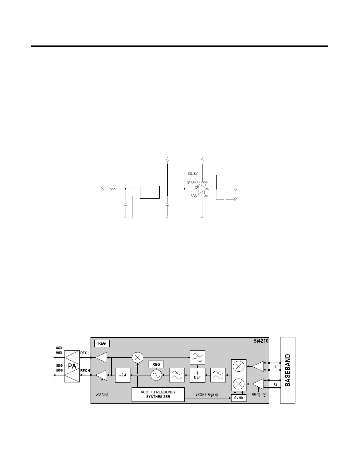
3.1 RF Transceiver General Description
The RF parts consist of a transmitter part, a receiver part, a frequency synthesizer part, a voltage
supply part, and a VCTCXO part.
The SI4210[U401] is a triple band transceiver IC suitable for GSM 900, DCS 1800 and PCS 1900
GPRS class 12 applications. This device integrated a receiver based on a low IF (100KHz)
architecture and a transmitter based on modulation loop architecture. And, the synthesizer part are
included in the IC, a complete dual band synthesizer with built in VCOs.
The transceiver employed a 3 wire serial interface to allow an external system controller to write the
control registers for dividers, receive path gain, power down setting, and other controls.
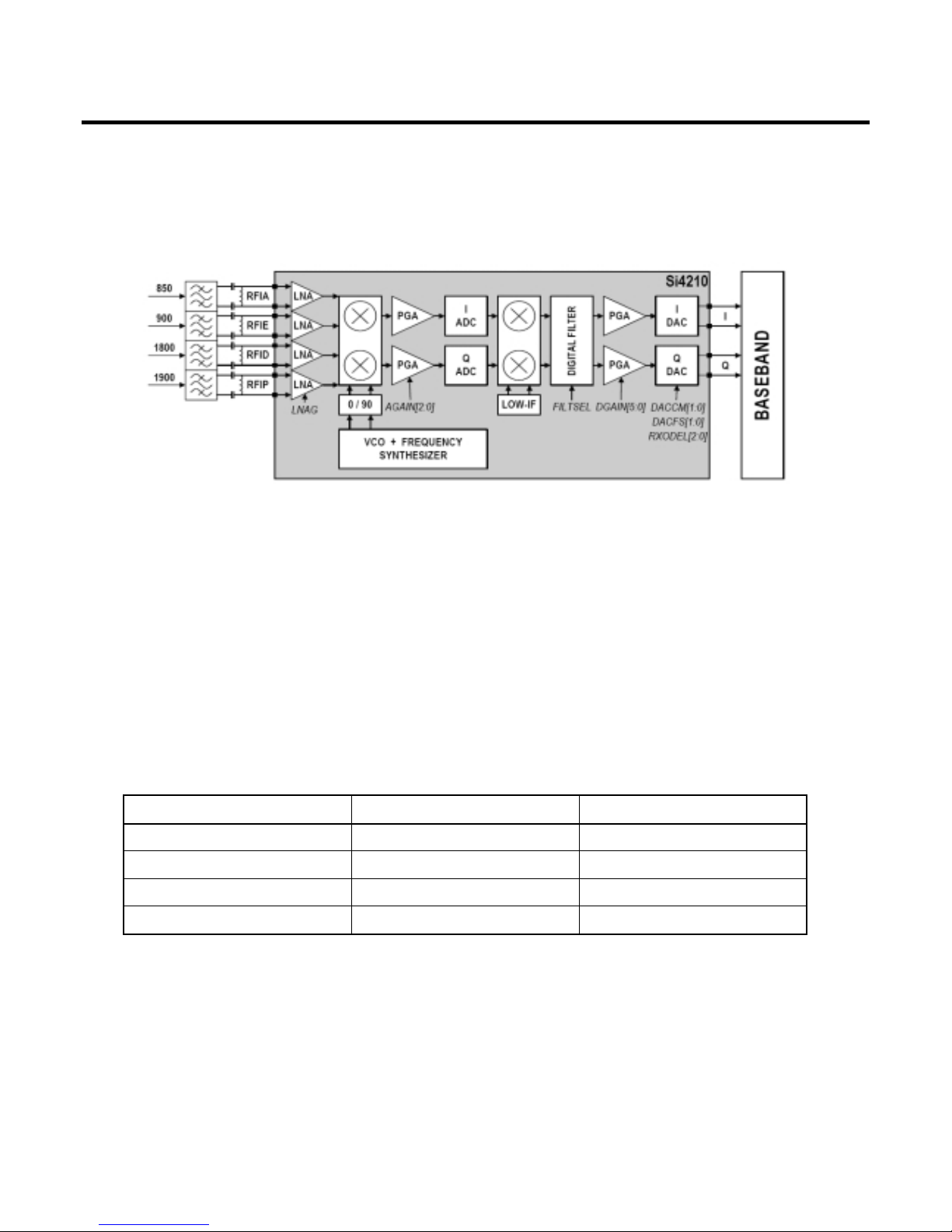
3.2 Receiver Part
The receiver part uses a low-IF receiver architecture that allows for the on-chip integration of the
channel selection filters, eliminating the external RF image reject filters and the IF SAW filter required
in conventional super-heterodyne architecture. The SI4210[U401] integrates three differential input
LNAs that are matched to the 200 Ohm balanced-output SAW filters through external LC matching
networks. A quadrature image-rejection mixer downconverts the RF signal to a 100kHz intermediate
frequency (IF) with the RFLO.
The mixer output is amplified with an analog programmable gain amplifier (PGA) and quadrature IF
signal is digitized with high resolution A/D converters (ADCs). The SI4210[U401] downconverts the
ADC output to baseband with a digital 100kHz quadrature LO signal. Digital decimation and IIR filters
perform channel selection to remove blocking and reference interference signals. After channel
selection, the digital output is scaled with digital PGA, which is controlled with the DGAIN[5:0] bits in
register 05h.The amplified digital output signal go through with DACs that drive a differential analog
signal onto the RXIP,RXIN,RXQP and RXQN pins to interface to standard analog ADC input baseband
ICx.
Table 3-1. Antenna(RSSI) Display
Antenna Bar Number Rx Power (dBm)
5≥-85
4≥-90
Antenna Display
3≥-95
2≥-100
2≥-105
1 <-105
3.2.1. RF Front End
RF front end consists of Antenna Switch Module with SAW filter for triple band(FL400), triple band
LNAs integrated in transceiver(U401).
The Received RF signals (EGSM 925MHz ~ 960MHz, DCS 1805MHz ~ 1880MHz, PCS 1850 ~
1990MHz) are fed into the antenna or mobile switch. An antenna matching circuit is between the
antenna and the mobile switch. The Antenna Switch(in FL400) is used for control the Rx and TX paths.
And, the input signals ANT1,ANT2 of a FL400 are directly connected to baseband controller to switch
either TX or RX path on and select bands. Ant S/W module(FL400) is an antenna switch module for
dual band phone. The logic and current is given below.
The receiver part uses a low-IF receiver architecture that allows for the on-chip integration of the
channel selection filters, eliminating the external RF image reject filters and the IF SAW filter required
in conventional super-heterodyne architecture. The SI4210[U401] integrates three differential input
LNAs that are matched to the 200 ohm balanced-output SAW filters through external LC matching
networks.
3. H/W Circuit Description
- 14 -
Figure 1. RECEIVER PART Block Diagram
Table 3-2. BAND/RTX SELECTION
ANT_SW1 ANT_SW2
GSM 850_EGSM RX L L
GSM-850_EGSM TX L H
DCS/PCS RX H L
DCS/PCS TX H H

3. H/W Circuit Description
- 15 -
3.2.2. Low IF
A quadrate image-rejection mixer downconverts the RF signal to a 100kHz intermediate frequency (IF)
with the RFLO . The RFLO frequency is between 1849.8 and 1918.8 MHz, and is divided by two for
EGSM modes. The RFLO frequency is between 1804.9 and 1879.9 MHz, and is divided by one for
DCS modes. The RFLO frequency is between 1929.9 and 1989.9 MHz, and is divided by one for PCS
modes. The mixer output is amplified with an analog programmable gain amplifier (PGA), which is
controlled with the AGAIN[2:0] bits in register 05h. The quadrate IF signal is digitized with high
resolution A/D converters (ADCs). The Si4210[U401] down-converts the ADC output to baseband with
a digital 100kHz quadrate LO signal. Digital decimation and IIR filters perform channel selection to
remove blocking and reference interference signals. The response of the IIR filter is programmable to
a high selectivity setting(CSEL=0) or a low selectivity setting (CSEL=1). After channel selection, the
digital output is scaled with digital PGA, which is controlled with the DGAIN[5:0] bits in register 05h.
3.2.3. Demodulator and Baseband Processing
The amplified digital output signal go through with DACs that drive a differential analog signal onto the
RXIP, RXIN, RXQP and RXQN pins to interface to standard analog ADC input baseband ICs. No
special processing is required in the baseband for offset compensation or extended dynamic range.
Compared to a direct-conversion architecture, the low-IF architecture has a much greater degree of
immunity to dc offsets that can arise from RF local oscillator(RFLO) self-mixing, 2nd order distortion of
blockers, and device 1/f noise.
3.3 Synthesizer Part
The Si4210[U401] integrates two complete PLLs including VCOs, varactors, resonators, loop filters,
reference and VCO dividers, and phase detectors. The RF PLL uses two multiplexed VCOs. The RF1
VCO is used for receive mode, and the RF2 VCO is used for transmit mode. The IF PLL is used only
during transmit mode. All VCO tuning inductors are also integrated. The IF and RF output frequencies
are set by programming the N-Divider registers, NRF1, NRF2, and NIF. Programming the N-Divider
register for either RF1 or RF2 automatically selects the proper VCO. The output frequency of each
PLL is as follows:
F
OUT
= N x fφ
A programmable divider in the input stage allows either a 13 or 26 MHz reference requency depending
on the choice of crystal. A 26 MHz reference clock can be divided by 2 using the DIV2 bit in Register
31h. The RF PLL phase detector update rate (fφ) can be programmed with the RFUP bit in register
31h to either fφ= 100 kHz or fφ = 200 kHz. The IF PLL always uses fφ = 200 kHz. Receive mode
should use fφ = 100 kHz in DCS 1800 and PCS 1900 bands, and fφ = 200 kHz in the E-GSM 900
bands. Transmit modes should always use fφ = 200 kHz.
3.3.1. VCTCXO
The VCTCXO module supply 26MHz reference clock and controlled by AFC input to generate a
precise system reference clock adjustment.
The 26 MHz clock(X500) consists of a TCXO(Temperature Compensated Crystal Oscillator) which
oscillates at a frequency of 13 MHz. It is used within the TRF6151C RF Main Chip, BB Analog chipset(IOTA), Digital chip-set(Calypso Lite).
3.4 Transmitter Part
The Transmitter part contains SI4210[U401] active parts, Power Amp Module[U400] and Antenna
Switch Module[FL400]. The transmit section of SI4210[U401] consists of an I/Q baseband pconverter,
an offset phaselocked loop (OPLL) and two 50 ohm output buffers that can drive external power
amplifiers. The RF GMSK outputs from the transmit VCO are fed directly to the RF power amplifiers.
The peak output power and the profile of the transmitted burst are controlled by means of incorporated
power control circuits inside of PA and DAC output. from the Baseband Controller. The PA outputs
pass to the antenna connector via Antenna Switch Module.
3. H/W Circuit Description
- 16 -
Figure 4. VC-TCXO Circuit
BT_26MHZ
26MHzX401
2
GND
3
OUT
VCC
4
VCONT
1
C428
1000p
RF2.85V
R550
100K
RF2.85V
1000p
C999
C430
1u
1000p
C429
15K
R425
C431
1000p
TCXO_OUT
AFC
Figure 3. TRANSMITTER PART Block Diagram

3. H/W Circuit Description
- 17 -
3.4.1. IF Modulator
The baseband converter(BBC) within the GSM chipset generates I and Q baseband signals for the
Transmit vector modulator. The modulator provides more than 40dBc of carrier and unwanted
sideband. Rejection and produces a GMSK modulated signal. The baseband software is able to
cancel out differential DC offsets in the I/Q baseband signals caused by imperfections in the D/A
converters. The TX-Modulator implements a quadrature modulator. A quadrature mixer upconverts the
differential I/Q signals with the IFLO to generate a SSB IF signal, which is filtered and used as the
reference input to the OPLL. The SI4210[U401] generates the IFLO frequency. The IFLO is divided by
two to generate the quadrature LO signals for the quadrature modulator.
3.4.2. OPLL
The OPLL consists of a feedback mixer, a phase detector, a loop filter, and a fully integrated
TXVCO.The TXVCO is centered between the DCS 1800 and PCS 1900 bands, and its output is
divided by 2 for the E-GSM 900 bands. The Si4206 generates the RFLO frequency between 1327 and
1402 MHz. To allow a single VCO to be used for the RFLO, high-side injection is used for the E-GSM
900 bands, and low-side injection is used for the DCS 1800 and PCS 1900 bands. Low-pass filters
before the OPLL phase detector reduce the harmonic content of the quadrature modulator and
feedback mixer outputs. The cutoff frequency of the filters is programmable with the FIF[3:0] bits in
register 04h. The OPLL requires no external duplexer to attenuate transmitter noise and spurious
signals in the receive band. Additionally, the output of the transmit VCO (TXVCO) is a constantenvelope signal which reduces the problem of spectral spreading caused by non-linearity in the PA
3.4.3. Power Ampifier Module
The RF3166[U400] is a triple-band GSM/DCS/PCS power amplifier module that incorporates an
indirect closed loop method of power control. The indirect closed loop is fully self-contained and it does
not require loop optimization. It can be driven directly from the DAC output in the baseband circuit. Onboard power control provides typical 50 dB of control range with an analog voltage input (Vapc).
Efficiency is 53% at GSM, DCS and PCS.
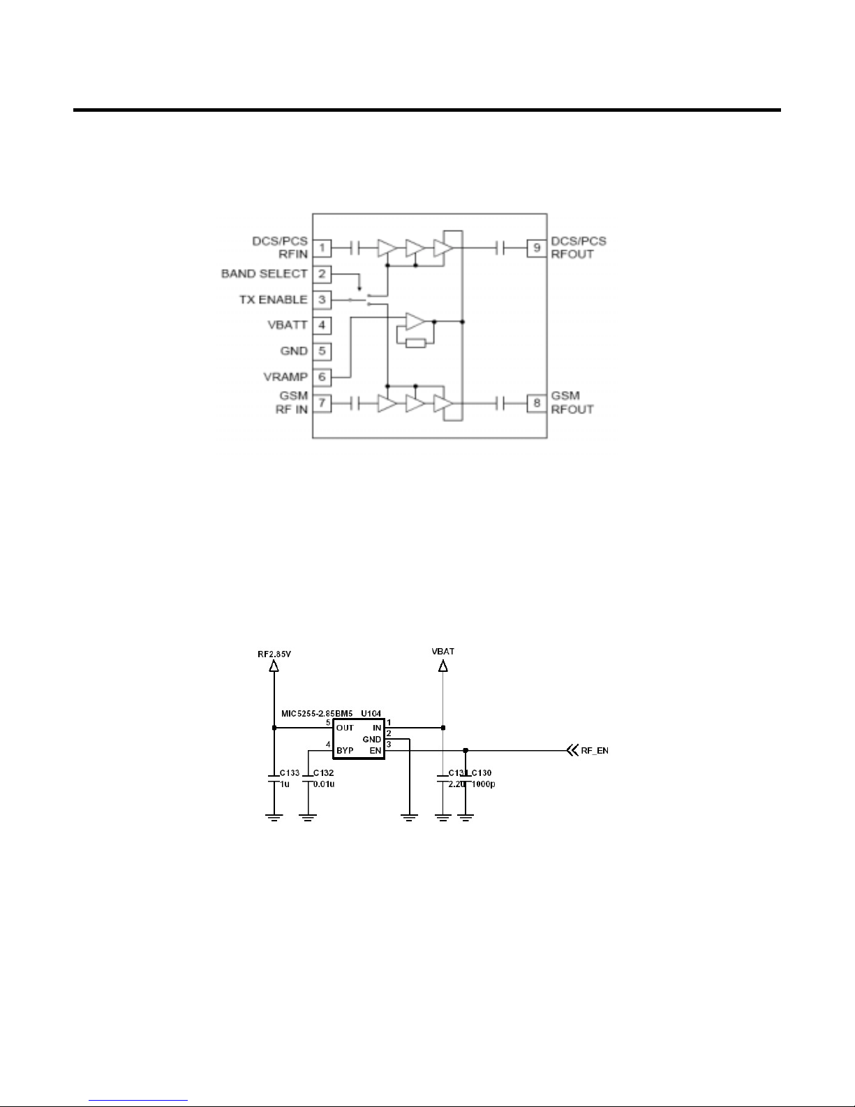
3.4.4. Power Supplies and Control Signals
An external regulator(U303) is used to provide DC power to RF part. Every RF component except
power amp module uses this external regulator.
3. H/W Circuit Description
- 18 -
Figure 4. POWER AMP
Figure 5 POWER SUPPLIE & CONTROL
14/89

3. H/W Circuit Description
- 19 -
3.5 Digital Baseband
A. General Description
• Calypso-Plus device is an evolution of Calypso(C035) device integrating hardware enhancements
targeting the implementation of a new range of user’s applications.
• It supports the digital baseband processing of GSM radio signals in switching circuit mode and
packet data mode up to class 12 in compliance with the ETSI specification of the GPRS protocol.
• The functional enhancement of the Calypso-Plus offer an increase computing performance of both
ARM7 based MCU and C54x based DSP sub-system in addition to numerous new connectivity.
Figure 7. Top level block diagram of the Calypso-Plus
The enhanced computing performances mainly rely on :
[ MCU Sub-system]
- 5.5Mbit Internal SRAM (with 0.5Mb shared with DSP)
- DMA to internal SRAM
- Page Mode Memory Interface
- Sizable 6 Chip-Select
- 2 Generic Purpose external interrupts
- Patch Unit
[ DSP Sub-system]
- 0.5Mb Program/Data Memory Extension shared with MCU
The new connectivity peripherals are :
- LCD controller parallel physical interface(6800 & 8080 protocol)
- USB client(W2FC)
- Multi Media and Secure Digital Card(MMC/SD) interface
- Memory Stick(MS) interface(using exclusive with MMC/SD)
- Audio and Data interface for external Bluetooth Modem connection
- Audio Codec serial interface(I2S)
- Smart Card physical interface (ISO-7816)
- NAND-Flash Interface
- Enhanced Keyboard controller
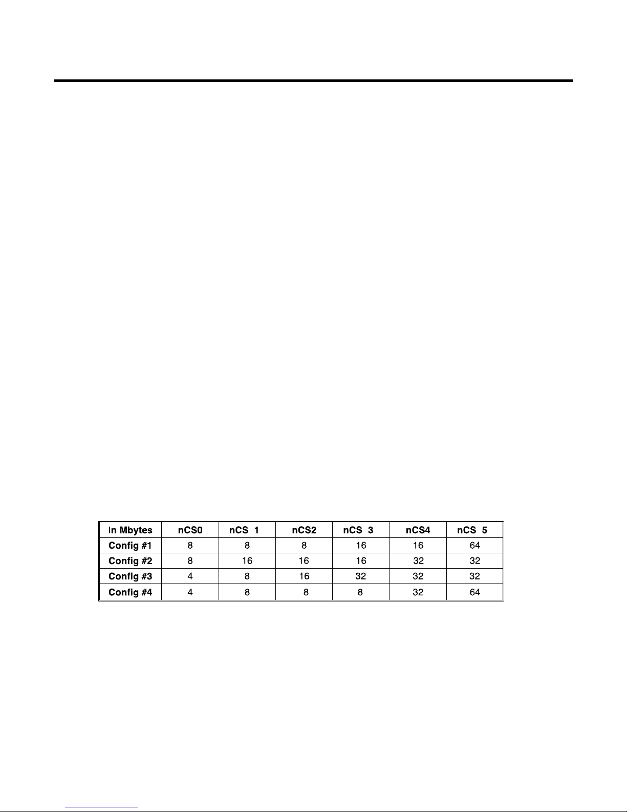
B. Memory Interface
Calypso-Plus has 6-sizable chip select port and can configure as follow :
3. H/W Circuit Description
- 20 -
Table 3. Configuration of addressable ranges

3. H/W Circuit Description
- 21 -
MG810C applies configuration #1 as its external memory interface, the external devices are connected
to as follow.
Calypso-Plus has NAND Flash interface and it allows NAND EEPROM as an mass external storage
facility. The interface implements a 8-bit parallel data bus in addition to the control signals for selecting
chip, writing/Reading, command and address latching, ready/busy status.
(MG810c does not use NAND I/F Ports of Calypso-Plus. NAND Memory is interfaced to MAP)
MG810C uses stacked memory MCP(pSRAM + NOR-Flash) as shown in (Figure 7.)
Table 4. External Device Spec. connected to memory interface
Figure 7. Memory interface scheme
Mirror bit only
MEMORY 256Mb NOR & 128 Mb pSRAM
100K
R309
C399
0.1u
V_FLASH
V_FLASH
VSS2
C5
WP_ACC
_CE1F
H2
_CE1S
J2
B5
_CE2F
_LB
C4
_OE
H3
_RSTF
D5
D4
_UB
C6
_WE
L6
RFU23
L7
L8
RFU24
RFU25
L9B4
RFU3
RFU4
B6
RFU5
B7
B8
RFU6
RFU7
B9
C2
RFU8
RFU9
C9
E5
RY__BY
J5
VCCF1
VCCF2
L5
J6
VCCS
G3
VSS1
J9
M1
NC4
M10
B2
RFU1
F5
RFU10
RFU11
F6
G5
RFU12
RFU13
G6
G8
RFU14
RFU15
H9
K2
RFU16
RFU17
K6
RFU18
K9
L2
RFU19
RFU2
B3
RFU20
L3
L4
RFU21
RFU22
DQ10
K5
DQ11
DQ12
J7
H7
DQ13
K8
DQ14
DQ15
H8
DQ2
K4
DQ3
H5
H6
DQ4
K7
DQ5
G7
DQ6
DQ7
J8
K3
DQ8
H4
DQ9
A1
NC1
A10
NC2
NC3
E4
A19
D7
E2
A2
A20
E6
E9
A21
F9
A22
A3
D2
A4
F3
A5
E3
D3
A6
C3
A7
C7
A8
E7
A9
D6
CE2S
DQ0
J3
DQ1
G4
J4
S71PL254JD0BFWTB0
U302
A0
G2
A1
F2
F7
A10
C8
A11
A12
D8
E8
A13
F8
A14
A15
D9
A16
G9
A17
F4
A18
R310
100K
0
R318
R317
NA
0.1u
C312
R316 0
R319
NA
A(5)
A(6)
A(7)
A(8)
A(9)
A(10)
A(1:23)
A(24)
TCXOEN
FDP
_CS1
D(0:15)
A(1)
A(2)
A(11)
A(12)
A(13)
A(14)
A(15)
A(16)
A(17)
A(18)
A(19)
A(20)
A(3)
A(21)
A(22)
A(4)
_CS5
_RD
_CS3
_BLE
_BHE
_WR
A(23)
D(0)
D(1)
D(10)
D(11)
D(12)
D(13)
D(14)
D(15)
D(2)
D(3)
D(4)
D(5)
D(6)
D(7)
D(8)
D(9)
_RDYMEM
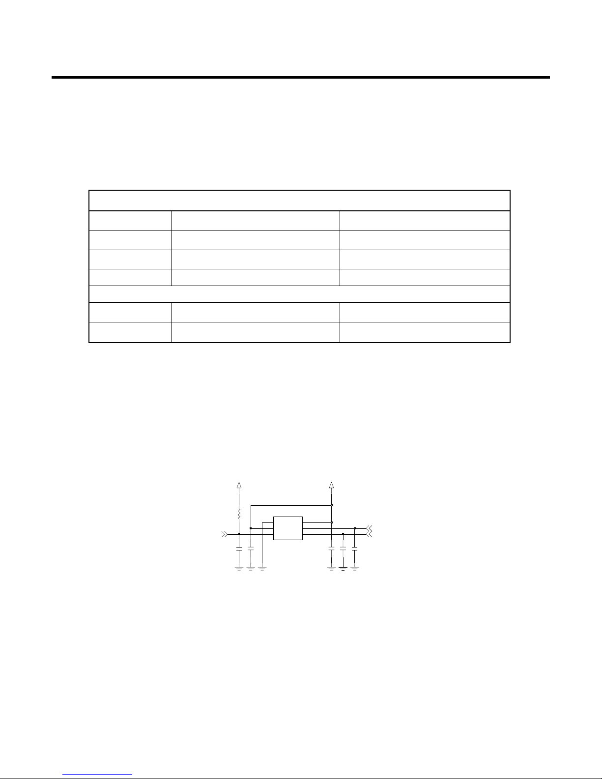
C. RF Interface (TPU, TSP block)
Calypso-Plus uses this interface to control ABB Processor and RF Processor with GSM Time Base.
D. SIM interface
SIM interface scheme is shown in (Figure 8.). SIM_IO, SIM_CLK, SIM_RST ports are used to
communicate DBB with ABB and the Charge Pump in ABB enables 1.8V/3V SIM operation
SIM_CLK : SIM Card reference clock SIM_PWCTRL : SIM Card power activation
SIM_RST : SIM Card async/sync reset SIM_RnW : SIM Card data line direction
SIM_IO : SIM Card bi-directional data line SIM_CD : SIM Card presence detection
3. H/W Circuit Description
- 22 -
TSP (Time Serial Port)
Resource Interconnection Description
TSPDO ABB & RF main Chip Control Data
TSPEN0 ABB ABB Control Data Enable Signal
TSPEN1 RF main Chip RF Control Data Enable Signal
TPU (Time Processing Unit) Parallel Port
TSPACT00 RESET_RF RF main Chip Reset Signal
TSPACT01 PA_ON Power Amp ON signal
Table 5. RF Interface Spec.
Figure 8. SIM Interface
SIM I/O CKTs
CLK
GND
I_O
RST
VCC
VPP
CN203
R226
20K
V_SIM
1u
C225
0.1u
C224
150p
C227
V_SIM
C226
150p
C223
22p
SIM_RST
SIM_IO SIM_CLK
3. H/W Circuit Description
- 23 -
Table 6. UART Interface Spec.
E. Serial Interface
Calypso-Plus has UART-IRDA and two UART Modem Drivers.
UART-IrDA (For Debugging Trace)
Resource Name Description
TX_IRDA TX Transmit Data
RX_IRDA RX Receive Data
UART MODEM1 (For PC-Sync & Download)
Resource Name Description
TX_MODEM1 TXD Transmit Data
RX_MODEM1 RXD Receive Data
DSR_MODEM1 DSR Data Set Ready
UART MODEM2 (for Bluetooth)
Resource Name Description
TX_MODEM2 TXD Transmit Data
RX_MODEM2 RXD Receive Data
RTS_MODEM2 RTS Ready to Send
CTS_MODEM2 CTS Clear to Send
F. USB Interface
The USB_W2FC module supports the implementation of a "Full-Speed" device fully compliant to USB
1.1 standard. It provides an interface between the MCU and the USB device and handles USB
transactions with minimal MCU intervention.
The USB_W2FC module supports one control endpoint (EP0), up-to fifteen (15) IN endpoints and upto fifteen (15) OUT endpoints. The exact endpoint configuration is software programmable. The
specific items configurable for each endpoint are the size in bytes, the direction (IN, OUT), the type
(Bulk/Interrupt or ISO), and the associated endpoint number.
The USB_W2FC module also supports three DMA channels for IN endpoints and three DMA channels
for OUT endpoints for either Bulk/Interrupt or ISO transactions. In operation, the USB requires a
48MHz clock generated by a dedicated embedded DPLL upon request. The USB module interface is
PVCI compliant. Therefore this module interfaces with the TI MCU RHEA bus via a RHEA-PVCI
bridge.
Calypso-Plus integrates differential drivers to allow a glue-less connection with any host. The required
3.3V VDD is provided by the VBUS signal taken from the USB connector.
- USB_DP : USB differential (+) line.
- USB_DM : USB differential (-) line.
- USB_PU_EN : USB pull-up enable.
- MAP_USB_P : MAP(Corelogic) USB differential(+) line
- MAP_USB_N : MAP(Corelogic) USB differential(-) line
- USB_PATH_SEL : choice either DBB or MAP(Corelogic)
3. H/W Circuit Description
- 24 -
Figure 9. USB interface diagram
G. Audio Circuits
All audio functions are performed in CL8237S4(MAP) and YMU783(MIDI IC). MP3/AAC decoding is
performed in CL8237S4 and MIDI ring-tone generation and DAC function of MP3/AAC, MIDI is
performed in YMU783. All analog audio signals (including voice signal) are mixed in YMU783 using
analog mixer stage and amplified with amplifier stage for headphone and speaker.
1) MP3, AAC Decoding (Corelogic, CL8237S4)
CL8237S4 is a multimedia processor. It includes Camera Interface, NAND Interface, LCD Interface,
ARM9 Processor, etc. In MG810c, CL8237S4 uses 27MHz X-tal(X201) for system clock. For Audio
function of MG810c, CL8237S4 performs storing, decoding MP3/AAC data. MP3/AAC data is stored in
NAND-Memory, which is connected to CL8237S4 via NAND Interface(NAND_D(0~7)). The MP3/AAC
data are decoded in CL8237S4 and the decoded data is transferred to MIDI IC(YMU783) via I2S
bus(I2S_WS, I2S_SCK, I2S_SDO). I2S bus is a standard digital audio bus.
3. H/W Circuit Description
- 25 -
Figure 10. Audio Block Diagram
2) MIDI IC(YMU783)
The MIDI IC(YMU783, YAMAHA) has three main functions. The first function is MIDI ring-tone
generation. The second function is a digital-to-analog conversion of decoded MP3/AAC data from
MAP(CL8237S4, CoreLogic). The third fucntion is a analog mixing and amplifying of voice signal from
ABB(TWL3016, TI)
3. H/W Circuit Description
- 26 -
NA
VDDPLL
B13
VDDS
B2
B5
VDDSD
H1
VDDUSB
VSS0E7VSS1G5VSS2
K6
L8
VSS3
VSSPLL
B14
D6
VSSQ
XCTS0
A11
XRTS0
D10
X_IN
C14
X_OUT
C13
R211
L13
TMS
TRST
N10
T_OUTL9T_VREF
K9
K10
T_VRO
H4
USBDM
H2
USBDP
P14
VDDAC
E6
VDDC0
VDDC1H5VDDC2
K7
L7
VDDC3
E8
VDDI0
VDDI1K8VDDI2
L6
VDDLCD
J5
N_RE_N
N6
P9
N_WE_N
L11
RTCK
B7
SD_D0
SD_D1
A7
SD_D2
B6
A6
SD_D3
SD_D4
E5
SD_D5
D5
SIN0
E10
SOUT0
D11
STROBE
A3
L14
TCK
TDI
P11
L10
TDO
N11
TESTMODE
M_SD13
F13
F14
M_SD14
E14
M_SD15
J14
M_SD2
M_SD3
J11
J10
M_SD4
M_SD5
H11
H14
M_SD6
M_SD7
H13
H10
M_SD8
M_SD9
G13
M_WR_N
A12
N8
N_ALE
P8
N_CLE
N_CS_N
N9
N_RDY
P10
N4
L_WR_N
MS_CS_N
A13
M_ADS
D14
B11
M_CS_N
B12
M_HOLD
F11
M_INTR
M_RD_N
A14
F10
M_RESET_N
M_SA0
E13
D13
M_SA1
E11
M_SA2
M_SD0
K11
J13
M_SD1
G14
M_SD10
G11
M_SD11
M_SD12
G10
K4
L_DA12
L_DA13L1L_DA14
L2
J4
L_DA15K2L_DA16
L_DA17
K1
L_DA2
P3
P2
L_DA3
L_DA4P1L_DA5
N2
N1
L_DA6
L_DA7
L5
L4
L_DA8
L_DA9
M2
P5
L_PCLK
N5
L_RD_N
E_D3
B9
D9
E_D4
E9
E_D5
E_D6
A10
B10
E_D7
E_D8
B3
A4
E_D9
P7
GPIO1_D0
GPIO1_D1
N7
LS_CS_N
P6
J1
L_ADS
L_CS_N
J2
P4
L_DA0
L_DA1
N3
M1
L_DA10
L_DA11
K5
N13
D_BCK
M13
D_LRCK
D_MSCK
N12
D_SCK
P13
D_SDA
P12
N14
D_SDATAIN
M14
D_SDATAOUT
E_D0
D7
D8
E_D1
E_D10
B4
D4
E_D11
E_D12
E4
A5
E_D13
B8
E_D14
E_D15
A8
A9
E_D2
F4
C_D0
C_D1E2C_D2
D1
G4
C_D3
C_D4
F2
E1
C_D5
C_D6
G2
F1
C_D7
C_HS
A1
C2
C_MSCK
C_PCLK
F5
C_PWDN
G1
C_RST
A2
C_SCK
D2
C1
C_SDA
B1
C_VS
CL8524SN
U202
AVDDTV
K14
K13
AVSSTV
0
R209
L_RD
C218
15p
4.7K
R338
R337
4.7K
V_IO
NA
R203
R208
0
TP207
R324
100K
1000p
C311
NA
R322
1M
R207
V_IO
C206
V_USB
1u 1u
C210C208
1u
C204
1u
10K
R331
47p47p
C209C207
R334
10K
10K
R332
L_WR
2V8_CAM 2V8_MAP
TP201
R326
0
TP206
1V5_MAP
L_CS
V_IO
R330
10K
R333
10K
1V5_MAP
C217
15p
47p
C201
L_ADS
R323
100
R204
NA
R328
10K
47p
C205
R205
10K
1u
34
C202
27MHz
X201FA-238_27MHz_9PF
12
C203
47p
10K
R329
L_DATA(16)
LCD_ID
TCH_RST
C_SDA
C_SCK
A(3)
A(8)
D(2)
D(3)
D(4)
D(5)
D(6)
D(7)
D(8)
D(9)
_WR
NAND_ALE
NAND_CLE
NAND_CE
NAND_RnB
NAND_RE
NAND_WE
MAP_USB_N
MAP_USB_P
L_DATA(5)
L_DATA(6)
L_DATA(7)
L_DATA(8)
L_DATA(9)
L_RD
L_WR
LCD_CS
MAP_HOLD
MAP_INT
_RDMAP_RESET
A(1)
A(2)
D(0)
D(1)
D(10)
D(11)
D(12)
D(13)
D(14)
D(15)
NAND_D(3)
NAND_D(4)
NAND_D(5)
NAND_D(6)
NAND_D(7)
L_ADS
L_CS
L_DATA(0)
L_DATA(1)
L_DATA(10)
L_DATA(11)
L_DATA(12)
L_DATA(13)
L_DATA(14)
L_DATA(15)
L_DATA(17)
L_DATA(2)
L_DATA(3)
L_DATA(4)
C_DATA(0)
C_DATA(1)
C_DATA(2)
C_DATA(3)
C_DATA(4)
C_DATA(5)
C_DATA(6)
C_DATA(7)
C_HS
C_MCLK
C_PCLK
C_RST
C_VS
I2S_SCK
I2S_WS
I2S_SDO
NAND_D(0)
NAND_D(1)
NAND_D(2)
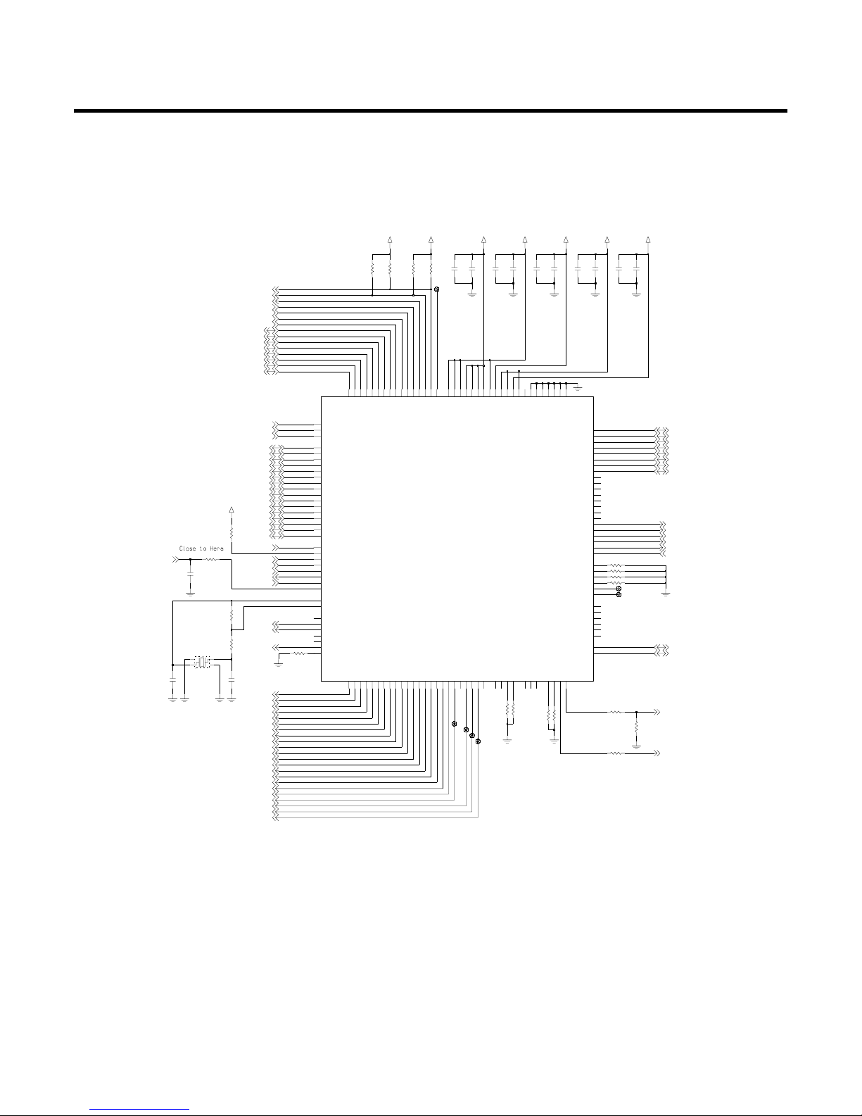
Figure 11. CL8237S4 circuits

i. MIDI function
MIDI data comes from DBB via Host I/F(D(0~7), A(0)). The data is decoded in YMU783 and converted
to analog signal via DAC block of YMU783. The analog midi signal is amplified with headphone
amplifier for ear-set, is amplified with speaker amplifier for speaker out. The amplified midi ring-tone
signal is delivered to speaker and MIDI sound is generated out from speaker to air.
ii. MP3/AAC DAC function
YMU783 has a I2S bus for digital audio. The decoded MP3/AAC digital data comes from
CL8237S4(MAP) via I2S bus(I2S_WS, I2S_SCK, I2S_SDO). The data goes to DAC block of YMU783
which converts the data to an analog audio signal. The converted analog MP3/AAC signal is amplified
with headphone amplifier for ear-set, is amplified with speaker amplifier for speaker out. The sound
path of MP3/AAC signal is same as MIDI signal.
In all of cases, the volume control is performed in volume stage of analog mixer and amplifier stage,
which is built in YMU783.
3. H/W Circuit Description
- 27 -
Figure 12. MIDI IC(YMU783, YAMAHA) circuits
MIDI_SPKPHN_HS_CKTs
C116 C117
100p100p
33K
R110
1u
NA
C122
C109
L103
100nH
I102
I101
C105
0.1u
0.1u
C118
C128
100p
3.3K
R107
I103
NA
R341
0.1u
C107
1u
C103
MIDI_INT
L102
100nH
C114
0.1u
C115
0.1u
68K
R109
0
R108
C101
10u
0.1u
C110C106
0.1u
C104
0.1u
0.1u
C129
0.1u
C130
C108
0.1u
22n
C123
C119
47p
C314
1000p
100nH
L105
1000p
C127
E1
H5
VREF
_CS
D8
B5
_IRQ
_RD
E8
_RST
E3
D9
_WR
100nH
L101
G7
NC8
H3
H7
NC9
E9
PLLCE2RXIN
SDI
B4
H2
SPOUT1L1
SPOUT1L2
J1
SPOUT1R1
H8
SPOUT1R2
J9
J2
SPOUT2L
J8
SPOUT2R
G1
SPVDDL
G9
SPVDDR
H1
SPVSSL
H9
SPVSSR
TXOUT
J7
B8
IOVDD1
IOVDD21
D2
D3
IOVDD22
IOVDD23
D4
C2
LED0
LED1_GPIO4
B2
LED2_GPIO5
C3
LRCK
C5
MTR
B1
NC1A1NC2
A9
E7
NC3
NC4F7NC5G3NC6G5NC7
DVSS2
EQ1L
F1
EQ1R
F9
F2
EQ2L
EQ2R
F8
EQ3L
G2
G8
EQ3R
J6
EXC
EXTIN
F3
EXTOUT
H6
C4
GPIO0
GPIO1
A3
B3
GPIO2
GPIO3
A2
G6
HPC
G4
HPOUTL_MONO
HPOUTR
J5
BBL
J3
H4
BBR
A4
BCLK
C8
CLKI
D0A8D1
A7
B7
D2
D3
C7
A6
D4
D5
B6
C6
D6
D7
A5
DVDD1C1DVDD2
C9
B9
DVSS1
D1
YMU783
U102
D7
A0
J4
AVDD
AVSS
C121
NA
_MIDI_RST
TCH_LDO_EN
D(0)
MCLK
I2S_SDO
VIBRATOR
HSOL
HSO_R
_MIDI_CS
MIDI_INT
_RD
_WR
SPK_RCV_N
SPK_RCV_P
HSO_L
D(7)
D(6)
D(5)
D(4)
D(3)
D(2)
D(1)
A(0)
I2S_SCK
I2S_WS
HSOR
3. H/W Circuit Description
- 28 -
3) Acoustic Function
The voice link is composed of two part. One is Up-link. The other is Down-link.
i. Up-link path.
A voice signal is converted to electrical signal with Microphone. The converted electrical voice signal is
amplified and converted to digital signal in ABB(TWL3016, TI). The converted digital data is encoded
to GSM voice standard in DBB(Calypso +).
The audio signal from main microphone goes to MICP of ABB and the voice signal from head-set to
HSMIC of ABB. The bias voltage for microphone is 2V for main mic. and 2.5V for head-set mic, which
bias voltage is generated in ABB(MICBIAS, HSBIAS)
Figure 13. Voice circuits of ABB(TWL3014)
Figure 14. Main Mic. Circuits.
NA
C110
100p
C109
C114
0.1u
0.1u
C113
100p
C117
SPKN1
A7
SPKN2
B7
A6
SPKP1
B6
SPKP2
HSMIC
A11
HSMICBIAS
B10
HSOL
A9
A10
HSOR
HSOVMID
B9
C9
MICBIAS
MICIN
A12
MICIP
B12
B8
EARN
A8
EARP
B11
AUXI
C8
AUXO
C112
NA
C116
100p
L102
100nH
0R129
100nH
L101
L105
100nH
R130 0
L104
100nH
L103
100nH
C118
100p
C115
4.7u
C111
NA
HSOL
MICN
HSMIC
HSOR
HSBIAS
MICBIAS
MICP
MAIN_MIC_CKTs
C126
2
G1
3
G2
G3
5
OUT
1
4
PWR
10u
MIC101
SP0102BE3
C313
100p
C125
100p
EVLC14S02050
VA307
0.1u
C322
100p
C124
100nH
L107
C120
0.1u
100p
C312
VA306
EVLC14S02050
L106
100nH
100nH
L104
MICBIAS
MICP
MICN
ii. Down-link path
A voice signal from ABB(HSOR, HSOL) goes to RX_IN, EXT_IN of YMU783. which ports are analog
voice input of analog mixer block. In case of using head-set, the analog mixer of YMU783 is set to
head-phone out path. The voice signal is amplified via head-phone amplifier and goes to earphone(HSO_R, HSO_L). In case of using main-receiver, the analog mixer is set to Speaker out
path(SPOUT_L) and the voice signal goes to main speaker/receiver(SPK_RCV_P, SPK_RCV_N).
H. KeyPad Switching & Scanning
Keypad Map
DBB supports 6x6 keymap and Switch-ON Key is connected directly to ABB as (Figure16.).
3. H/W Circuit Description
- 29 -
Figure 15. Down-link circuits related with YMU783
Table 7. Keypad Map
C116 C117
100p100p
33K
R110
1u
NA
C122
C109
L103
100nH
C128
100p
3.3K
R107
0.1u
C107
L102
100nH
C114
0.1u
C115
0.1u
68K
R109
0
R108
C101
10u
0.1u
C110
0.1u
C129
0.1u
C130
C108
0.1u
22n
C123
C119
47p
100nH
L105
1000p
C127
E1
H5
VREF
100nH
L101
G7
NC8
H3
H7
NC9
E9
PLLCE2RXIN
H2
SPOUT1L1
SPOUT1L2
J1
SPOUT1R1
H8
SPOUT1R2
J9
J2
SPOUT2L
J8
SPOUT2R
G9
SPVDDR
H9
SPVSSR
TXOUT
J7
NC1A1NC2
A9
E7
NC3
NC4F7NC5G3NC6G5NC7
EQ1L
F1
EQ1R
F9
F2
EQ2L
EQ2R
F8
EQ3L
G2
G8
EQ3R
J6
EXC
EXTIN
F3
EXTOUT
H6
G6
HPC
G4
HPOUTL_MONO
HPOUTR
BBL
J3
H4
BBR
C121
NA
HSOL
HSO_R
SPK_RCV_N
SPK_RCV_P
HSO_L
HSOR
 Loading...