

Page 1

MODEL: MDT505(MDS505V/W)SERVICE MANUAL
Internal Use Only
Website http://biz.lgservice.com
MINI HOME THEATER
SERVICE MANUAL
MODEL:
CAUTION
BEFORE SERVICING THE UNIT, READ THE “SAFETY PRECAUTIONS”
IN THIS MANUAL.
0102,SEPTEMBER21827947NFA:ON/P
MDT505 (MDS505V/W)
Page 2

CONTENTS
SECTION 1 ........ GENERAL
SECTION 2 ........ CABINET & MAIN CHASSIS
SECTION 3 ........ ELECTRICAL
SECTION 4 ........ REPLACEMENT PARTS LIST
1-1
Page 3
SECTION 1. GENERAL
SERVICING PRECAUTIONS
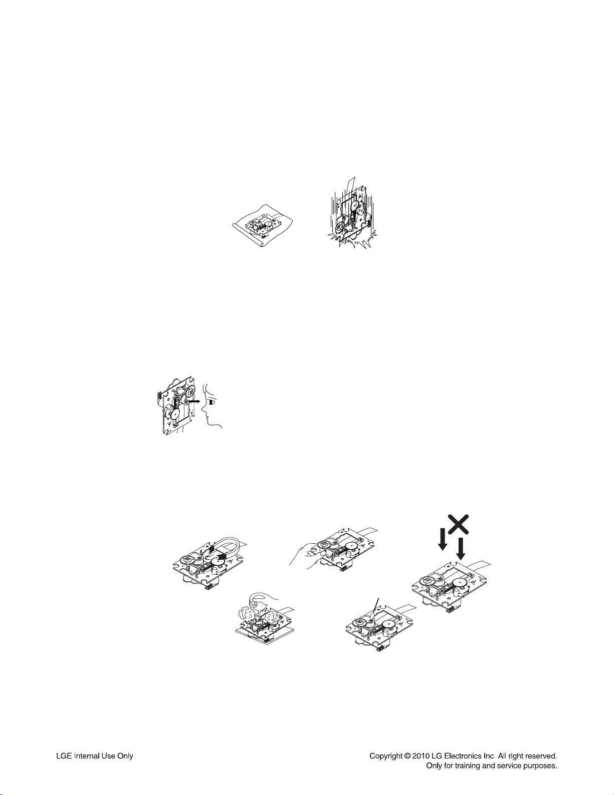
NOTES REGARDING HANDLING OF THE PICK-UP
1. Notes for transport and storage
1) The pick-up should always be left in its conductive bag until immediately prior to use.
2) The pick-up should never be subjected to external pressure or impact.
2. Repair notes
Storage in conductive bag
1) The pick-up incorporates a strong magnet, and so should never be brought close to magnetic materials.
2) The pick-up should always be handled correctly and carefully, taking care to avoid external pressure and
impact. If it is subjected to strong pressure or impact, the result may be an operational malfunction and/or
damage to the printed-circuit board.
3) Each and every pick-up is already individually adjusted to a high degree of precision, and for that reason
the adjustment point and installation screws should absolutely never be touched.
4) Laser beams may damage the eyes!
Absolutely never permit laser beams to enter the eyes!
Also NEVER switch ON the power to the laser output part (lens, etc.) of the pick-up if it is damaged.
NEVER look directly at the laser beam, and don’t allow
contact with fingers or other exposed skin.
5) Cleaning the lens surface
If there is dust on the lens surface, the dust should be cleaned away by using an air bush (such as used
for camera lens). The lens is held by a delicate spring. When cleaning the lens surface, therefore, a cotton
swab should be used, taking care not to distort lens.
Drop impact
Pressure
Magnet
How to hold the pick-up
Cotton swab
Conductive Sheet
6) Never attempt to disassemble the pick-up.
Spring has excess pressure. If the lens is extremely dirty, apply isopropyl alcohol to the cotton swab.
(Do not use any other liquid cleaners, because they will damage the lens.) Take care not to use too much
of this alcohol on the swab, and do not allow the alcohol to get inside the pick-up.
1-2
Pressure
Page 4
NOTES REGARDING COMPACT DISC PLAYER REPAIRS
1. Preparations
1) Compact disc players incorporate a great many ICs as well as the pick-up (laser diode). These components
are sensitive to, and easily affected by, static electricity. If such static electricity is high voltage, components
can be damaged, and for that reason components should be handled with care.
2) The pick-up is composed of many optical components and other high-precision components. Care must be
taken, therefore, to avoid repair or storage where the temperature or humidity is high, where strong magnetism is present, or where there is excessive dust.
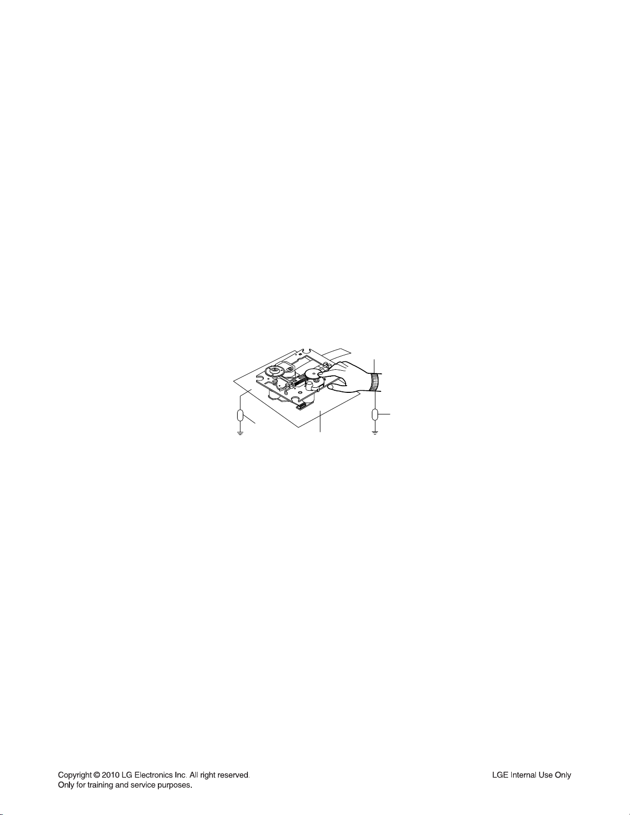
2. Notes for repair
1) Before replacing a component part, first disconnect the power supply lead wire from the unit
2) All equipment, measuring instruments and tools must be grounded.
3) The workbench should be covered with a conductive sheet and grounded.
When removing the laser pick-up from its conductive bag, do not place the pick-up on the bag. (This is
because there is the possibility of damage by static electricity.)
4) To prevent AC leakage, the metal part of the soldering iron should be grounded.
5) Workers should be grounded by an armband (1 MΩ)
6) Care should be taken not to permit the laser pick-up to come in contact with clothing, in order to prevent static electricity changes in the clothing to escape from the armband.
7) The laser beam from the pick-up should NEVER be directly facing the eyes or bare skin.
Armband
Resistor
(1 MΩ)
Resistor
(1 MΩ)
Conductive
Sheet
1-3
Page 5
ESD PRECAUTIONS
Electrostatically Sensitive Devices (ESD)
Some semiconductor (solid state) devices can be damaged easily by static electricity. Such components
commonly are called Electrostatically Sensitive Devices (ESD). Examples of typical ESD devices are integrated
circuits and some field-effect transistors and semiconductor chip components. The following techniques should
be used to help reduce the incidence of component damage caused by static electricity.
1. Immediately before handling any semiconductor component or semiconductor-equipped assembly, drain off
any electrostatic charge on your body by touching a known earth ground. Alternatively, obtain and wear a
commercially available discharging wrist strap device, which should be removed for potential shock reasons
prior to applying power to the unit under test.
2. After removing an electrical assembly equipped with ESD devices, place the assembly on a conductive surface
such as aluminum foil, to prevent electrostatic charge buildup or exposure of the assembly.
3. Use only a grounded-tip soldering iron to solder or unsolder ESD devices.
4. Use only an anti-static solder removal device. Some solder removal devices not classified as "anti-static" can
generate electrical charges sufficient to damage ESD devices.
5. Do not use freon-propelled chemicals. These can generate electrical charges sufficient to damage ESD
devices.
6. Do not remove a replacement ESD device from its protective package until immediately before you are
ready to install it. (Most replacement ESD devices are packaged with leads electrically shorted together by
conductive foam, aluminum foil or comparable conductive materials).
7. Immediately before removing the protective material from the leads of a replacement ESD device, touch the
protective material to the chassis or circuit assembly into which the device will by installed.
CAUTION : BE SURE NO POWER IS APPLIED TO THE CHASSIS OR CIRCUIT, AND OBSERVE ALL OTHER
SAFETY PRECAUTIONS.
8. Minimize bodily motions when handing unpackaged replacement ESD devices. (Otherwise harmless motion
such as the brushing together of your clothes fabric or the lifting of your foot from a carpeted floor can generate
static electricity sufficient to damage an ESD device).
CAUTION. GRAPHIC SYMBOLS
THE LIGHTNING FLASH WITH APROWHEAD SYMBOL. WITHIN AN EQUILATERAL TRIANGLE, IS
INTENDED TO ALERT THE SERVICE PERSONNEL TO THE PRESENCE OF UNINSULATED
“DANGEROUS VOLTAGE” THAT MAY BE OF SUFFICIENT MAGNITUDE TO CONSTITUTE A RISK OF
ELECTRIC SHOCK.
THE EXCLAMATION POINT WITHIN AN EQUILATERAL TRIANGLE IS INTENDED TO ALERT THE
SERVICE PERSONNEL TO THE PRESENCE OF IMPORTANT SAFETY INFORMATION IN SERVICE
LITERATURE.
1-4
Page 6
SERVICE INFORMATION FOR EEPROM
POWER ON
DVD LOGO status
(N0 disc status)
Remote control
pause keyÖ1Ö4Ö7Ö2 in order
Press number 0~9, press character
A~F (1~6 for a while)
Use arrow key (▲/▼/◀/▶) to
move to appropriate position and
make changes
Press pause key once
DETECT NEW EEPROM
(OPTION EDIT SCREEN)
NAME
OPT 1
OPT 2
OPT 3
OPT 4
OPT 5
OPT 6
OPT 7
OPT 8
OPT 9
OPT A
HEX
A5
06
85
B4
00
08
91
01
80
00
Change will be applied
when power OFFÖON
1-5
Page 7

HOW TO UPDATE AUDIO MICOM & DVD PROGRAMS
1. How to update AUDIO MICOM program.
[Update using CD]
1. Change the filename to download as “MDS715_(Version).HEX”. Only upper cases are permitted.
ex) MDS715 : “MDS715_0709081.HEX”
2. Copy the file to the root folder of a CD and burn it.
3. Insert the CD to the SET, and move to the DVD function.
Then the upgrade process will be started with the upgrade information.
4. If the upgrade process is complete, the set will be rebooted with “Complete” message.
[Update using USB]
1. Change the filename to download as “MDS715_(Version).HEX”. Only upper cases are permitted.
ex) MDS715 : “MDS715_0709081.HEX”
2. Copy the file to the root folder of USB storage.
3. After Home-menu is displayed on Screen of SET, Put the USB into the SET.
Then the upgrade process will be started with the upgrade information.
4. If the upgrade process is complete, the set will be rebooted with “Complete” message.
2. How to update DVD program.
[Update using CD]
1. Copy DVD program(ex: LG_MDS715LD1_Version.Rom) to Root folder of CD, and burn it.
ex) P:LG_MDS715LD1_0911180.Rom
2. Insert the CD to the SET, then after a while the CD tray will be opened with upgrade information on
the screen.
3. Remove the CD, and press “PLAY” key in remote controller.
4. Remove and reconnect the power cable when it changes to logo screen from upgrade information.
Then the upgrade process is completed.
[Update using USB]
1. Copy DVD program(ex: LG_MDS715LD1_Version.Rom) to Root folder of the formatted USB and burn it.
ex) P:\LG_MDS715LD1_0911180.Rom
2. After Home-menu is displayed on Screen of SET, Put the USB into the SET.
Then the upgrade process will be started with the upgrade information.
3. Remove the USB, press "PLAY" key of the remote controller.
4. Remove and reconnect the power cable when it changes to logo screen from upgrade information.
Then the upgrade process is completed.
1-6
Page 8

SPECIFICATIONS
• GENERAL
Power supply 110~240 V, 50/60 Hz
Power consumption Refer to main label
Dimensions (W x H x D) 273 x 333 x 339 mm without foot
Net Weight (Approx.) 5.7 kg
Operating temperature 41 °F to 95 °F (5 °C to 35 °C)
Operating humidity 5 % to 90 %
Bus Power supply (USB) DC 5V 500mA
• INPUTS/ OUTPUTS
VIDEO OUT 1.0 V (p-p), 75 Ω, sync negative, RCA jack x 1
COMPONENT VIDEO OUT (Y) 1.0 V (p-p), 75 Ω, sync negative, RCA jack x 1,
(Pb)/(Pr) 0.7 V (p-p), 75 Ω, RCA jack x 2
ANALOG AUDIO IN 0.6 Vrms, 47 kΩ, RCA jack (L, R) x 1
PORT. IN 0.5 Vrms (3.5 mm stereo jack)
• TUNER
FM Tuning Range 87.5 to 108.0 MHz or 87.50 to 108.00 MHz
AM Tuning Range 522 to 1 620 kHz, 520 to 1 710 kHz or 522 to 1 710 kHz
• AMPLIFIER
Stereo mode 150 W + 150 W (4 Ω at 1 kHz)
Surround mode
Front 150 W + 150 W (4 Ω at 1 kHz)
Center 70 W (6 Ω at 1 kHz)
Surround 70 W + 70 W (6 Ω at 1 kHz)
Subwoofer 200 W (3 Ω at 60 Hz)
1-7
Page 9

• SPEAKERS
Front speaker (MDS505V)
rekaeps 2 yaW 2 epyT
4 ecnadepmI Ω
Rated Input Power 150 W
W 003 rewop tupnI .xaM
Net Dimensions(W x H x D) 240 x 387 x 336 mm
gk 5 thgieW teN
Passive Subwoofer (MDS505W)
rekaeps 1 yaW 1 epyT
3 ecnadepmI Ω
Rated Input Power 200 W
W 004 rewop tupnI .xaM
Net Dimensions(W x H x D) 261 x 331 x 409 mm
gk 5.6 thgieW teN
1-8
Page 10

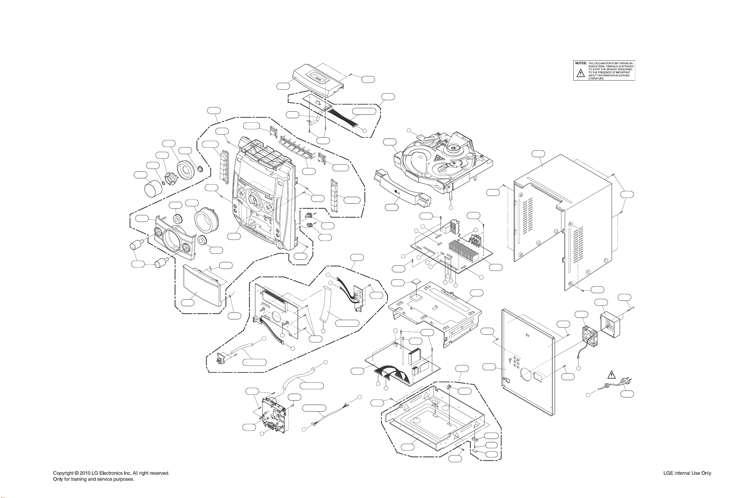
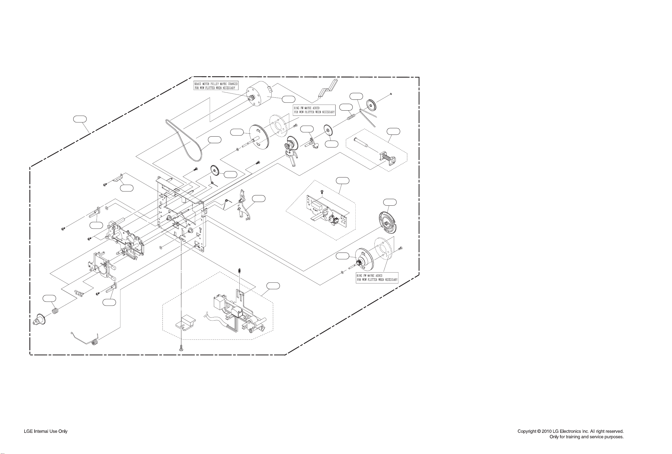
SECTION 2
CABINET & MAIN CHASSIS
CONTENTS
EXPLODED VIEWS..................................................................................................................................... 2-3
1. CABINET AND MAIN FRAME SECTION (MDT505) ................................................................................ 2-3
2. TAPE DECK MECHANISM SECTION ...................................................................................................... 2-5
3. DVD DECK MECHANISM SECTION (DVM-H1723) ................................................................................ 2-7
4. SPEAKER SECTION .............................................................................................................................. 2-11
5. PACKING ACCESSORY SECTION .......................................................................................................2-13
2-1
Page 11

MEMO
2-2
Page 12
EXPLODED VIEWS
1. CABINET AND MAIN FRAME SECTION (MDT505)
272
iPod
464
A45
251
260
259
254
255
256
261
257
252
262
A42
263L
464
261
464
258
250
270L
FRONT
271
464
269
464
464
265
264
J
E
270R
CABLE1
263R
A43
USB
P
A26
A26
A
276
A26
274
464
B
463
A
B
463
O
464
MAIN
C
D
F
464
463
273
E
G
H
P
I
275
A46
J
464
279
455
VOLUME
253
CABLE2
464
A00
278
CABLE3
SMPS
N
463
464
451
A44
277
L
L
C
D
464
F
A47
464
O
464
CABLE4
464
G
I
H
268
N
300
464
CABLE5
M
M
267A
267A
464
266
464
464
267
267
2-3 2-4
Page 13
2. TAPE DECK MECHANISM SECTION (A/R & A/S : RIGHT A/R DECK)
A00
009
003
001
007
037
015
006
017
020
019
022
018
A01
023
025
011
A02
009
2-5 2-6
Page 14
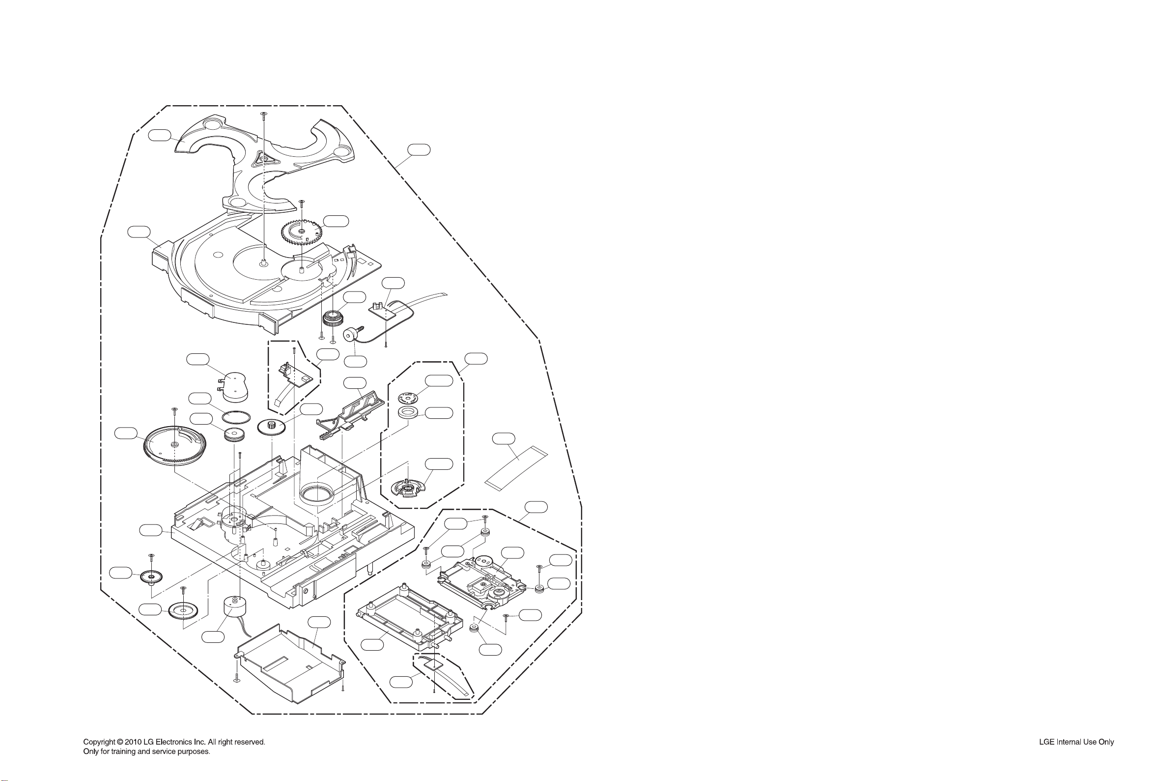
3. DVD DECK MECHANISM SECTION (DVM-H1723)
151
A26
153A
159
156
153
177
167
172
166
170
162
163
175
164
181
165
155
173
180
169A
169B
169C
430
012
A02
012
010
137
A01
430
012
430
035
2-7 2-8
Page 15
MEMOMEMO
2-9 2-10
Page 16
4. SPEAKER SECTION
4-1. FRONT SPEAKER (MDS505V)
A60
2-11
Page 17
4-2. PASSIVE SUBWOOFER (MDS505W)
A90
2-12
Page 18
5. PACKING ACCESSORY SECTION
808 Battery
811 RCA Cable, 1 Pin(Black)
900 Remote Control
803 Packing, Casing
824 AM Loop Antenna
825 FM Wire Antenna
801 Owner’s Manual
804 Bag
802 Box
2-13
Page 19

MEMO
2-14
Page 20

SECTION 3
ELECTRICAL
CONTENTS
ELECTRICAL TROUBLESHOOTING GUIDE .................................................................................... 3-2
DETAILS AND WAVEFORMS ON SYSTEM TEST AND DEBUGGING ................................ 3-16
WIRING DIAGRAM ................................................................................................................................... 3-29
BLOCK DIAGRAM .................................................................................................................................... 3-31
CIRCUIT DIAGRAMS ............................................................................................................................... 3-33
1. SMPS - POWER CIRCUIT DIAGRAM ................................................................................................. 3-33
2. MAIN - MICOM CIRCUIT DIAGRAM .................................................................................................... 3-35
3. MAIN - PWM CIRCUIT DIAGRAM ....................................................................................................... 3-37
4. MAIN - AMP CIRCUIT DIAGRAM ........................................................................................................ 3-39
5. MAIN - DECK CIRCUIT DIAGRAM ...................................................................................................... 3-41
6. MAIN - MPEG CIRCUIT DIAGRAM ..................................................................................................... 3-43
7. MAIN - SERVO CIRCUIT DIAGRAM ................................................................................................... 3-45
8. MAIN - I/O CIRCUIT DIAGRAM ........................................................................................................... 3-47
9. VFD CIRCUIT DIAGRAM ..................................................................................................................... 3-49
10. MIC & USB CIRCUIT DIAGRAM .......................................................................................................... 3-51
11. VOLUME CIRCUIT DIAGRAM ............................................................................................................. 3-53
12. IPOD CIRCUIT DIAGRAM (OPTIONAL PART) ................................................................................... 3-55
13. KARAOKE CIRCUIT DIAGRAM (OPTIONAL PART) ........................................................................... 3-57
CIRCUIT VOLTAGE CHART ................................................................................................................. 3-59
PRINTED CIRCUIT BOARD DIAGRAMS ......................................................................................... 3-61
1. MAIN P.C.BOARD ................................................................................................................................ 3-61
2. SMPS P.C.BOARD ............................................................................................................................... 3-65
3. FRONT(VFD / USB & MIC / VOLUME) P.C.BOARD ........................................................................... 3-67
4. IPOD P.C.BOARD (OPTIONAL PART) ................................................................................................ 3-69
5. KARAOKE P.C.BOARD (OPTIONAL PART) ....................................................................................... 3-69
3-1
Page 21
ELECTRICAL TROUBLESHOOTING GUIDE
1. SMPS BOARD
No power.
Check the AC
line pattern.
YES
Check fuse F901.
YES
Check C978
voltage (3.9 V).
YES
Check C963
voltage (5.6 V).
YES
NO
NO
NO
NO
Connect the open line.
Replace F901.
Check BD901 “+”
to “
-
” Pin impedance .
Check 3.7 V lines short.
Replace PC972, IC902’s components.
Check SMPS second part lines short.
Check MAIN or AMP board short.
Low impedance:
Replace IC901, BD901.
Check IC901
Vcc voltage (10 V ~ 30 V).
YES
Replace SMPS board.
NO
Replace PC951, PC972, IC901.
Check around IC901’s components
(Short, Open).
3-2
Page 22

ELECTRICAL TROUBLESHOOTING GUIDE
No sound.
Check IC961
Vcc voltage(34 V ~ 43 V).
YES
Check C955 voltage
(25 V or 36 V).
YES
Replace IC961, IC901 or
SMPS board.
NO
NO
Check no power list, AC input voltage.
Check AMP module short.
Replace PC951, IC901.
3-3
Page 23

ELECTRICAL TROUBLESHOOTING GUIDE
2. FRONT BOARD
Power on.
“WELCOME”
Display
on VFD ok?
YES
Volume LED
(LD301~LD315)
turn on?
NO
NO
PN301 cable
connection ok?
YES
PN301 Pin1,2,3,6
power ok?
YES
PN301
Pin7, 8, 9, 10 data signal
ok?
YES
IC301
check ok?
YES
Digitron (DIG301) ok?
PN301 Pin21
+12 V ok?
NO
NO
NO
NO
NO
NO
Check 36p FFC cable.
Check SMPS board.
Check MAIN board.
Replace IC301.
Replace DIG301.
Check SMPS board.
YES
When you turn
the volume knob, count
is change?
YES
FRONT board ok.
NO
YES
Check
PN301 Pin11,13,29~36
data signal.
YES
Replace LED (LD301~LD315).
PN301 Pin22, 26
signal ok?
YES
Check MAIN board.
3-4
NO
NO
Check Main board.
Check 5p FFC cable.
Page 24

ELECTRICAL TROUBLESHOOTING GUIDE
3. NO AUDIO CHECK
CD/DVD Disc
or USB play.
IC602 Pin4, 5,
6, 7, 8 I2S input
signal ok?
YES
IC602 I2S
output signal
ok?
YES
A
PORTABLE function.
NO
NO
Check IC500.
Check IC602.
AUX function.
IC200
Pin7,8 audio
L/R ok?
YES
B
HEADPHONE output.
NO
Check JK201.
IC200
Pin21, 22 audio
L/R ok?
YES
B
NO
Check JK301.
IC301
Pin 1, Pin 7
audio signal
ok?
YES
Front Board
CN301 Pin1,3 audio
signal ok?
YES
Check Front Board stage
and JK301.
NO
NO
Check IC301.
Check CN301 and
Connection.
3-5
Page 25

ELECTRICAL TROUBLESHOOTING GUIDE
IPOD function.
YES
IPOD B/D
CN201 Pin27,
28 audio L/R
ok?
YES
IPOD B/D
CN202 Pin13, 15
ok?
YES
MAIN B/D
PN201 Pin13, 15
ok?
YES
IC200
Pin26, 27 audio
signal ok?
YES
B
NO
NO
NO
NO
Check IPOD
connection or CN201.
Check IPOD Board.
Check 15p Harness
and connection.
Check IC251.
TUNER Function.
Pin23,24 audio
L/R ok?
B
A
Pin42, 43, 44 I2S
clock ok?
Pin41 I2S output
signal ok?
Pin4~8 I2S
input signal
I2S output signal
IC701 audio
output signal
Check AMP IC output
stage and JK701(JK702).
IC200
IC200
IC200
IC602,
ok?
IC602
ok?
ok?
YES
YES
YES
YES
YES
YES
YES
NO
NO
NO
NO
NO
NO
Check Tuner (TU345)
and Antenna
connection.
Check IC500 and
X500.
Check IC200.
Check IC500.
Check IC602.
Check IC701.
3-6
Page 26

ELECTRICAL TROUBLESHOOTING GUIDE
4. NO VIDEO CHECK
COMPONENT video out.
IC201 Pin2, 3, 4
video signal ok?
IC201 Pin11, 12, 13
video signal ok?
Check JK201.
CVBS video out .
IC252 Pin3
video signal ok?
YES
YES
NO
NO
NO
Check IC500.
Check IC500.
Check IC201.
YES
IC252 Pin4
video signal ok?
YES
IC201 Pin14
video signal ok?
YES
Check JK201.
NO
NO
IC252
Pin6 LOW
signal?
YES
Check IC252.
Check IC201.
3-7
NO
Check Micom (IC101).
Page 27

ELECTRICAL TROUBLESHOOTING GUIDE
CVBS video out
(IPOD video).
IPOD B/D
CN201 Pin23 video
signal ok?
YES
IPOD B/D
CN202 Pin10 ok?
YES
MAIN B/D
IC250 Pin4 ok?
YES
IC252 Pin1
video signal ok?
YES
IC252 Pin4
video signal ok?
NO
NO
NO
NO
NO
Check IPOD connection
or CN201.
Check IPOD Board.
Check 15p Harness cable
and connection.
Check IC250.
IC252
Pin6 HIGH
signal?
NO
Check Micom (IC101).
YES
IC201 Pin14
video signal ok?
YES
Check JK201.
NO
YES
Check IC252.
Check IC201.
3-8
Page 28

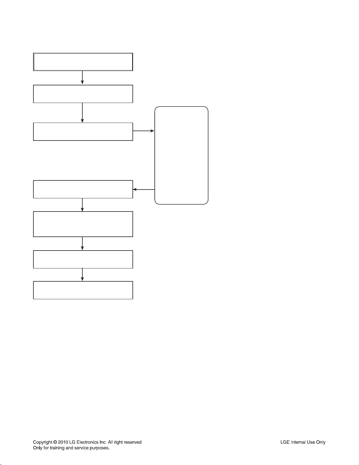
5. SYSTEM OPERATION FLOW
POWER ON.
1. Initializes SERVO, DSP & RISC registers.
2. Write RISC code to SDRAM.
3. Reset RISC.
Show LOGO.
YES
Tray closed?
NO
Tray close to closed position.
SLED at inner
side?
NO
SLED moves to inner position.
1. Judge whether have disc and disc type.
2. Jump to related disc reading procedure.
Recieve
OPEN/ CLOSE
Key?
YES
YES
NO
NO
1. Execute Pressed Key & IR Key.
2. System operation routine loop.
1. Stop Playback & Open Tray.
2. Display tray open message & LOGO.
YES
Receive
CLOSE Key?
YES
3-9
Page 29

6. TEST & DEBUG FLOW
TEST.
YES
Check the
AC voltage Power PCBA (110 V
or 220 V).
YES
Switch on the Power PCBA.
YES
Are the
DC Voltage outputs OK? (from the SMPS).
YES
Are 3.7, 5.6, 12 and
28 V(36V) DC outputs normal on
Main PCBA?
YES
Update
FLASH successfully?
YES
NO
NO
NO
NO
Check the POWER PART.
Check the POWER PART.
Check the regulators or diode.
1. Check 27 MHz system clock.
2. Check system reset circuit.
3. Check FLASH R/W enable signal PRD,
RWR.
4. Check FLASH Memory related circuit.
NO
A
Replace FLASH.
3-10
Page 30

A
YES
Power On.
YES
Show LOGO?
YES
Does Tray
move inside when it
is not at closed
position?
NO
NO
Flash
Memory operates
properly?
YES
SDRAM
works properly?
YES
MT1389SE/GH
VIDEO outputs
properly?
YES
Check AV cable
connection to TV set.
Normal
OPEN_SW,
CLOSE_SW
signal?
NO
NO
NO
NO
Check connection lines between
FLASH & MT1389SE/GH and
the FLASH access time
whether is suitable or not.
Check connection lines
between SDRAM(IC503) &
MT1389SE/GH and the
SDRAM is damaged.
Check the related circuit of
MT1389SE/GH IC500 Pin139,
143, 145, 146.
Check the load OPEN &
CLOSE switch.
B
YES
YES
Normal
TROPEN & TRCLOSE
signal?
YES
Normal
LOAD+ & LOAD-
signal?
YES
Check FFC cable connection
between main PCBA and
loader. (MECHA)
3-11
NO
NO
Check the Tray control IO Pin
on MT1389SE/GH and IC401.
Check the Tray control MOTOR &
SERVO circuit IC400.
Page 31

B
YES
Does
the SLED move to inner
side when it is at outer
position?
YES
Do not put in disc
and close tray.
NO
Motor
Driver M_STBY
Pin is high?
YES
Motor
Driver SLD
Pin is High?
YES
SLED+ and
SLED- output
properly?
YES
Check the cable connection
with MECHA.
NO
NO
NO
Check the connection line of
M_STBY.
Check the related circuit of
SLD.
Check the amp circuit on motor
driver.
Optical Lens
has movements for
searching Focus?
YES
C
NO
Proper
Focus outputs
to motor driver?
YES
Proper F+ & F-
outputs?
YES
Check cable connection with
pick-up head.
3-12
NO
NO
Check Focus connection on
MT1389SE/GH
Check the amp circuit on motor
and motor driver.
driver.
Page 32

C
YES
Laser
turns on when
reading disc?
YES
Put disc in?
YES
Disc ID is correct?
NO
NO
NO
DVDLD or
CDLD output
property?
YES
Collector
voltage of power transistor
is OK?(Q400, Q401)
YES
Check cable connection
between transistor output and
pick-up head(23p FFC).
Laser off.
Proper
RF signal on
MT1389SE/GH.
NO
NO
NO
Check the laser power circuit
on MT1389SE/GH and
connecting to power transistor.
(Q400, Q401).
Check the related circuit on
laser power transistor.
Check the related circuit on
MT1389SE/GH RF signal.
YES
Does sPindle rotate?
YES
D
NO
YES
Check the RF connection
between S3053 and MT1389SE/GH.
Proper
SPinDLE signal on
MT1389SE/GH.
YES
SPNP
& SPNN output
properly?
YES
Check the cable connection
between sPindle and main
PCB(15p FFC).
3-13
NO
NO
Check the SPinDLE related
circuit on MT1389SE/GH.
Check the sPindle control amp
circuit of motor driver.
Page 33

D
YES
Focus on ok?
YES
Track On OK?
YES
NO
NO
Proper
signals on A, B, C,
D of MT1389SE/GH.
YES
Proper
CD_DVDCT signal on
MT1389SE/GH.
YES
Check CD_DVDCT connection
between S3053 and
MT1389SE/GH.
Proper
CD_DVDCT signal on
MT1389SE/GH.
YES
Proper
TRACK signal
on MT1389SE/GH.
NO
NO
NO
NO
Check connections between
MT1389SE/GH and pick-up head.
Check the related circuit on
MT1389SE/GH CD_DVDCT.
Check the related circuit on
MT1389SE/GH.
Check the TRACK connection
on MT1389SE/GH and motor driver.
Disc Playback?
YES
E
NO
YES
T+ & T- output
properly?
YES
Check cable connection
on pick-up head.
Check RF signal waveform.
3-14
NO
Check the tracking control amp
circuit on motor driver.
Page 34

E
YES
Normal Audio
output when disc
playback?
YES
TEST END.
NO
IC602(PWM IC)
received correct data
stream?
YES
Normal
PWM IC out?(IC602).
YES
Check AMP IC
(IC701, 702, 703).
NO
NO
Check connection between
IC500 BCK, LRCK, ADATA0,
ADATA1, ADATA2(Pin157,
158, 160, 161, 162).
Check the related circuit of
PWM IC
3-15
Page 35

DETAILS AND WAVEFORMS ON SYSTEM TEST AND DEBUGGING
4
1
2
3
1. SYSTEM 27 MHz CLOCK,RESET,FLASH R/W SIGNAL
1)
MT1389SE/GH
2)
MT1389SE/GH
Power Cord in
main clock is at 27 MHz(X500)
1
FIG 1-1
reset is high active.
P_CTL
DVD_RST
RESET_IN
2
3
4
FIG 1-2
3-16
Page 36

3) Flash R/W enable signal during download(Downloading)
5
6
7
5
SF_DI
SF_DO
2. SDRAM CLOCK
1)
MT1389SE/GH
DCLK = 93 MHz, Vp-p = 2.2, Vmax = 2.7 V
main clock is at 27 MHz(X500)
6
FIG 1-3
SDCLK
7
FIG 2-1
3-17
Page 37

3. VIDEO PART-1 (100% FULL COLOR-BAR)
8 9
11
8
10
9
10
CVBS_I Y
11
Pb Pr
3-18
Page 38

4. VIDEO PART-2 (100% FULL COLOR-BAR)
12 13
14 15
12
14
13
CVBS COMP_Y
15
COMP_Pb COMP_Pr
3-19
Page 39

5. SERVO OPEN/CLOSE SIGNAL
17
16
19 18
1) Tray open/close waveform
OPENSW
CLOSESW
OPEN
CLOSE
FIG 5-1
3) Tray open waveform
OPENSW
2) Tray close waveform
OPENSW
16
CLOSESW
17
OPEN
18
19
16
CLOSE
FIG 5-2
16
17
18
19
CLOSESW
OPEN
CLOSE
17
18
19
FIG 5-3
3-20
Page 40

20
22
23
21
6. SLED CONTROL RELATED SIGNAL (NO DISC CONDITION)
SLD
M-STBY
SL+
SL-
FIG 6-1
20
21
22
23
3-21
Page 41

7. LENS CONTROL RELATED SIGNAL(NO DISC CONDITION)
24
26
25
28
27
29
FOD
F+
F-
24
25
26
FIG 7-1
8. LASER POWER CONTROL RELATED SIGNAL(NO DISC CONDITION)
MDI1
DVDLD
CDLD
FIG 8-1
27
28
29
3-22
Page 42

9. DISC TYPE JUDGEMENT WAVEFORMS
30
32
31
F+
PU_DET
RF
FIG 9-1 (DVD)
F+
PU_DET
30
31
32
31 : This signal can see using special debug program
30
31
RF
32
FIG 9-2 (DVD)
3-23
Page 43

F+
35
34
33
33
PU_DET
RF
F+
PU_DET
RF
34
35
FIG 9-3 (CD)
34 : This signal can see using special debug program
33
34
35
FIG 9-4 (CD)
3-24
Page 44

10. FOCUS ON WAVEFORMS
37
39
38
36
36 : This signal can see using special debug program
PU_DET
FOD
F+
F-
PU_DET
FOD
F+
F-
36
37
38
39
FIG 10-1 (DVD)
36
37
38
39
FIG 10-2 (CD)
3-25
Page 45

40
42 41
11. SPINDLE CONTROL WAVEFORMS (NO DISC CONDITION)
FIG 11-1
SPinD
40
SP-
41
SP+
42
3-26
Page 46

46 45
44
12. TRACKING CONTROL RELATED SIGNAL(System checking)
43
43 : This signal can see using special debug program
PU_DET
PU_DET
43
TRO
TRO
44
T-
T+
T-
T+
PU_DET
TRO
45
46
FIG 12-1(DVD)
PU_DET
43
TRO
44
T-
45
T+
46
FIG 12-2(CD)
3-27
Page 47

MEMO
3-28
Page 48

MIC/USB
PCB
JOG PCB
WIRING DIAGRAM
TUNER
MODULE
DC FAN
AUX
JACK
23P
CN400
2P
23P
15P
CN401
3 CD CHANGER MD
P7708
2P
5.1 CH SPK TERMINAL
SMPS PCB
MAIN
PCB
8P
PN102
CN301
8P
P1001
PN301
36P
9P
P8502
6P
DECK
MECHANISM
5P
36P
CN302
5P
8P
P8501
PN304
CN200
4P
15P
PN201
15P 10P
CN102
2P
CN502
FRONT PCB
CN501
CN101
7P
PN101
IPOD PCB
CN202
CN952
CN951
3-29 3-30
2P
KARAOKE
PCB
Page 49

BLOCK DIAGRAMS
DECK S/W
PLAY/REC L/R
Deck
SOL/MOTOR
REC_BIAS
EXP_DATA,CLK
REC/PB_MUTE
HA12237F
Cassette
Deck ASP
TAPE
S-24CS16A01
REC_L/R
EEPROM
REMOCON
MODULE
HALL,LEAF
MCLK,BCLK
LRCLK,DATA
EEPROM
DATA,CLK
9.8304 MHz
LC87F5N
C8A
AUDIO
MICOM
(3.3V)
SPI(4P)DVD_RST
KIA7027
RESET
KIA7027
PWR_SENS
DSP_BSY
DSP_IBO
PWM_RST
DATA,CLK
PWM/DSP_CLK
PWM/DSP_DATA
PS9850
DSP/
PWM
Modulat
AMP_SD
AMP_OTW
AMP_PDN
Power Amp
FAN_AD
FAN
FAN_CTRL
FL
FR
S/W
TAS5614
RR
C/T
RL
Tuner
Aux-IN
Portable
IPOD
USB
MIC
H/PHONE
Composite
Component
D+, D-
IPOD VIDEO
/ CVBS
R/G/B
PR/Y/PB
NJM2505
VIDEO NOISE
ISOLATION
S4308
OP AMP
MC4580
OP AMP
THS7314
VIDIO FUNC
CS5346
ADC
H/P_ L/R
UART
NLASB
3157
DFT2G
VIDEO SW
LRCLK, BCLK
MCLK
5346_DATA
MIC L/R
IPOD VIDEO
CVBS
Y/G
Pb/B
Pr/R
27 MHz
MTK1389GH
MPEG
DATA
CP2.0
IPOD
RST,CLK
HY57V
64614
20HG
SDRAM
DMA[0-10]
DB[0-15]
SCL
W25Q
16BY
FLASH
SDA
KSC24
1021CS
EEPROM
SCL
SDA
6302_DO
6302_DI
OPEN/CLOSE
FOCUS/SLED
SPINDLE/TRACKING
6315_CLK
6315_STB
PT6302
VFD
DRIVER
GR[1-12]
SG[1-16]
VFD
MD_DVD, MD_CD
LD_DVD, LD_CD
VR_DVD, VR_CD
Motor
Driver
S3053
/S8082
A, B, C, D, E, F, RF
F+/-, T+/-
SLED+/SPINDLE+/LOAD+/OPEN/CLOSE
PICK-UP
Motor
MDS715:5.1ch
MDT505:2.1ch
MDD305 : 2ch
TJ3965D
3.3V LDO
TO
PWM/TUNE
R
KIA78R05
5V
TO USB
LM39102
5V LDO
TO IPOD
LM39102
5V LDO
TO MPEG
MO8706EN
DC/DC3.3V
TO MPEG
3-31 3-32
Page 50

CIRCUIT DIAGRAMS
1. SMPS - POWER CIRCUIT DIAGRAM
12
11
10
9
8
IMPORTANT SAFETY NOTICE
WHEN SERVICING THIS CHASSIS, UNDER NO
CIRCUMSTANCES SHOULD THE ORIGINAL DESIGN BE
MODIFIED OR ALTERED WITHOUT PERMISSION
FROM THE LG CORPORATION. ALL COMPONENTS
SHOULD BE REPLACED ONLY WITH TYPES IDENTICAL
TO THOSE IN THE ORIGINAL CIRCUIT. SPECIAL
COMPONENTS ARE SHADED ON THE SCHEMATIC
FOR EASY IDENTIFICATION.
THIS CIRCUIT DIAGRAM MAY OCCASIONALLY DIFFER
FROM THE ACTUAL CIRCUIT USED. THIS WAY,
IMPLEMENTATION OF THE LATEST SAFETY AND
PERFORMANCE IMPROVEMENT CHANGES INTO
THE SET IS NOT DELAYED UNTIL THE NEW SERVICE
LITERATURE IS PRINTED.
NOTE :
1. Shaded(
2. Voltages are DC-measured with a digital voltmeter
) parts are critical for safety.
Replace only with specified part number.
during Play mode.
7
6
5
4
3
2
CAUTION:
Danger if fuse is incorrectly replaced.
1
A
Replace only with the type identical to fuse rating
and(or) model name described in main label.
B C D E F G H I J K L M N O P Q R ST
Warning
Parts that are shaded are critical with
respect to risk of fire or electrical shock.
MDS715
EBY60928901 REV 4.1
SMPS
2010. 09. 15
3-33 3-34
Page 51

2. MAIN - MICOM CIRCUIT DIAGRAM
12
11
10
9
8
7
6
5
4
3
2
1
MDS715
MAIN #001 MICOM
EBY60749301 REV 7.1
A
B C D E F G H I J K L M N O P Q R ST
3-35 3-36
Page 52

3. MAIN - PWM CIRCUIT DIAGRAM
12
11
10
9
8
7
6
5
4
3
2
1
MDS715
MAIN #002 PWM
EBY60749301 REV 7.1
A
B C D E F G H I J K L M N O P Q R ST
3-37 3-38
Page 53

4. MAIN - AMP CIRCUIT DIAGRAM
12
11
10
9
8
7
6
5
4
3
2
1
MDS715
MAIN #003 AMP
EBY60749301 REV 7.1
A
B C D E F G H I J K L M N O P Q R ST
3-39 3-40
Page 54

5. MAIN - DECK CIRCUIT DIAGRAM
12
11
10
9
8
7
6
5
4
3
2
1
MDS715
MAIN #004 DECK
EBY60749301 REV 7.1
A
B C D E F G H I J K L M N O P Q R ST
3-41 3-42
Page 55

6. MAIN - MPEG CIRCUIT DIAGRAM
12
11
10
9
8
7
6
5
4
3
2
1
MDS715
MAIN #005 MPEG
EBY60749301 REV 7.1
A
B C D E F G H I J K L M N O P Q R ST
3-43 3-44
Page 56

7. MAIN - SERVO CIRCUIT DIAGRAM
12
11
10
9
8
7
6
5
4
3
2
1
MDS715
MAIN #006 SERVO
EBY60749301 REV 7.1
A
B C D E F G H I J K L M N O P Q R ST
3-45 3-46
Page 57

8. MAIN - I/O CIRCUIT DIAGRAM
12
11
10
9
8
7
6
5
4
3
2
1
A
B C D E F G H I J K L M N O P Q R ST
MDS715
MAIN #007 I/O
EBY60749301 REV 7.1
3-47 3-48
Page 58

9. VFD CIRCUIT DIAGRAM
12
11
10
9
8
7
6
5
4
3
2
1
MDS715/MD505/MDD305
VFD(FRONT)
EBY60729301 REV 6.2
A
B C D E F G H I J K L M N O P Q R ST
3-49 3-50
Page 59

10. MIC & USB CIRCUIT DIAGRAM
12
11
10
9
8
7
6
5
4
3
2
1
A
B C D E F G H I J K L M N O P Q R ST
MDS715/MDT505/MDD305/MCT565
MIC & USB
EBY60729401 REV 6.2
3-51 3-52
Page 60

11. VOLUME CIRCUIT DIAGRAM
12
11
10
9
8
7
6
5
4
3
2
1
MDS715/MDT505/MDD305
MAIN VR & JOG VOL
A
B C D E F G H I J K L M N O P Q R ST
EBY60729501 REV 2.2
3-53 3-54
Page 61

12. IPOD CIRCUIT DIAGRAM (OPTIONAL PART)
12
11
10
9
8
7
6
5
4
3
2
1
MDS715/MDT505-IPOD
EBY60729701 REV 5.2
A
B C D E F G H I J K L M N O P Q R ST
3-55 3-56
Page 62

13. KARAOKE CIRCUIT DIAGRAM (OPTIONAL PART)
12
11
10
9
8
7
6
5
4
3
2
1
A
B C D E F G H I J K L M N O P Q R ST
MDS715/MDT505/MDD305
NO-KEY
EBY60729601 REV 4.1
3-57 3-58
Page 63

CIRCUIT VOLTAGE CHART
NO. IC Symbol NAME/TYPE SPEC. VOLTAGE
1
2
3
4
5
6
IC101
MICOM
IC200
ADC IC
IC400
MOTOR
DRIVE
IC503
SDRAM
IC504
FLASH
IC602
PWM
LC87F5NC8A
VDD: 14,40,55,89
CS5346-CQZR
LVC:5
VLS:36
VD:46
VA:14
GND: 13, 31, 32
S3053
VCC:8,19
EM638165TS-6G
VDD: 1,3,9,14,27,43,49
MX25L1605DM21-12G
VDD:8
PS9850
VDD : 1,16,21,24,29,32,35,40,
43,48,57,59,60,61,64
VDD: +3.0 ~ +5.5V
VLS,VD,VLC:
1.71~5.25V
VA:3.1~5.25V
VCC: +4.3 ~ 13.2V VCC:+4.98V
VDD: +3 ~ +3.6V VCC: +3.33V
VDD: +2.7 ~ +3.6V VDD: +3.31V
IOVDD : +2.97V ~ +3.63V IOVDD : +3.28V
VDD 14 PIN: +3.28V
40,55,89 PIN : +3.28V
VLS,VD,VLC:3.35V
VA:5.2V
NO. LOCA. NO. Capacity Spec.(V)
1 BD901 600 127.3 373.3
2 C901 150 uF 450 127.3 373.3
3 C902 150 uF 450 127.3 373.3
4 C909 4.7 uF 50 19.6 19.6
5 C910 22 uF 50 22.0 22.0
6 C913 22 uF 50 22.2 22.2
7 C952 470 uF 50 43.1 43.1
8 C955 470 uF 50 43.1 43.1
9 C961 470 uF 50 43.1 43.1
10 C963 1000 uF 10 7.32 7.32
11 C965 47 uF 50 38.6 38.6
12 C966 1000 uF 25 12.6 12.6
13 C967 100 uF 10 4.96 4.96
14 C971 1000 uF 10 3.92 3.92
15 C978 220 uF 10 3.92 3.92
16 C979 220 uF 10 5.8 5.8
17 D901 600 251.0 474.0
18 D906 400 44.0 86.0
19 D907 400 77.2 178.0
20 D910 400 84.4 195.0
21 D951 200 95.2 181.0
22 D961 40 44.4 44.4
23 D962 60 57.6 57.6
24 D963 400 404.0 404.0
25 D964 400 60.0 60.0
26 D971 60 14.6 34.4
27 IC901 32 19 19
28 IC902 32 20.8 20.8
29 IC961 43 42.2 42.2
30 Q901 600 301.0 540.0
100V - 10% 240V/50Hz+10%
Voltage(V) Voltage(V)
3-59 3-60
Page 64

PRINTED CIRCUIT BOARD DIAGRAMS
1. MAIN P.C.BOARD
(TOP VIEW)
3-61 3-62
Page 65

MAIN P.C.BOARD
(BOTTOM VIEW)
3-63 3-64
Page 66

2. SMPS P.C.BOARD
MDS715
EAX35194121 REV 4.2
2010. 06. 11
NOTE) Warning
Parts that are critical with respect to risk
of fire or electrical shock.
3-65 3-66
Page 67

3. FRONT(VFD / USB & MIC / VOLUME) P.C.BOARD
3-67 3-68
Page 68

4. IPOD P.C.BOARD (OPTIONAL PART)
(TOP VIEW) (BOTTOM VIEW)
5. KARAOKE P.C.BOARD (OPTIONAL PART)
3-69 3-70
Page 69

MEMO MEMO
3-71 3-72
 Loading...