

Page 1

MINI Hi-Fi SYSTEM
SERVICE MANUAL
MODEL : MCD102 (MCS102F)
CAUTION
BEFORE SERVICING THE UNIT, READ THE “SAFETY PRECAUTIONS”
IN THIS MANUAL
.
MODEL : MCD102 (MCS102F)
SERVICE MANUAL
http://biz.lgservice.com
P/NO : AFN32840849 FEBRUARY, 2007
Page 2

1-1
CONTENTS
SECTION 1
GENERAL
SERVICING PRECAUTIONS......................................1-2
• NOTES REGARDING HANDLING OF THE PICK-UP
•
NOTES REGARDING COMPACTDISC PLAYER REPAIRS
ESD PRECAUTIONS...................................................1-4
LOCATION OF USERS CONTROLS.........................1-5
SPECIFICA TIONS........................................................1-7
SECTION 2
EXPLODED VIEWS
CABINET EXPLODED VIEW......................................2-1
TAPE DECK MECHANISM EXPLODED VIEW........2-3
1. TAPE DECK MECHANISM
(A/S & A/S : RIGHTA/S DECK)........................2-3
2. TAPE DECK MECHANISM
(A/S & A/S : LEFTA/S DECK) ..........................2-5
CD MECHANISM EXPLODED VIEW.........................2-7
SPEAKER EXPLODED VIEW ....................................2-9
MODEL : MCS102F ...............................................2-9
PACKING ACCESSORY VIEW.................................2-13
SECTION 3
AUDIO PART ELECTRICAL
AUDIO ELECTRICAL
TROUBLESHOOTING GUIDE....................................3-1
1. POWER (SMPS)................................................3-1
2. P-SENS...............................................................3-2
3. VKK CHECK.......................................................3-2
4. MICOM PART CHECK I ....................................3-2
5. MICOM PART CHECK II ...................................3-3
6. IC103(KS4CD21CS) CHECK............................3-4
7. FLD DISPLAY CHECK ......................................3-5
8. PWM MODULATION PART CHECK................3-6
9. POWER AMPPART CHECK............................3-7
10. AUX FUNCTION CHECK..................................3-8
11. TUNER FUNCTION CHECK.............................3-9
12. TAPE FUNCTION CHECK..............................3-10
13. T APE PLAY PAR TCHECK..............................3-11
14. TAPE REC PART CHECK...............................3-12
INTERNAL BLOCK DIAGRAM OF ICs...................3-13
1. ES6838 ..............................................................3-13
2. HA12237F..........................................................3-14
3. PS9829B............................................................3-15
4. PT6324...............................................................3-15
5. STR-S6757IF1905 ............................................3-16
6. T AS5142.............................................................3-17
7. U1739EJ2V1UD00/KF2_E...............................3-18
WIRING DIAGRAM....................................................3-20
BLOCK DIAGRAM.....................................................3-22
1. SMPS BLOCK DIAGRAM...............................3-22
2. MAIN & FRONT BLOCK DIAGRAM ..............3-24
SCHEMATIC DIAGRAMS .........................................3-26
1. SMPS SCHEMATIC DIAGRAM.......................3-26
2. MAIN SCHEMATIC DIAGRAM........................3-28
3. AMP SCHEMATIC DIAGRAM..........................3-30
4. DECK SCHEMATIC DIAGRAM.......................3-32
5. FRONT SCHEMATIC DIAGRAM.....................3-34
PRINTED CIRCUIT DIAGRAMS...............................3-36
1. MAIN P.C.BOARD............................................3-36
2. SMPS P.C.BOARD ..........................................3-40
3. FRONT P.C.BOARD........................................3-42
SECTION 4
CD PART ELECTRICAL
CD ELECTRICAL TROUBLESHOOTING GUIDE....4-1
1. CD PART TROUBLESHOOTING.....................4-1
2. USB PART TROUBLESHOOTING...................4-9
WAVEFORMS OF MAJOR CHECK POINT............4-10
SCHEMATIC DIAGRAMS .........................................4-13
1. CD SCHEMATIC DIAGRAM...........................4-13
2. USB SCHEMATIC DIAGRAM.........................4-15
PRINTED CIRCUIT DIAGRAM.................................4-17
CD P.C.BOARD....................................................4-17
SECTION 5
REPLACEMENT PARTS LIST
........5-1
Page 3
1-2
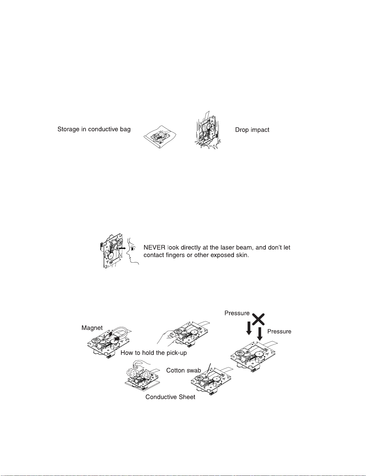
NOTES REGARDING HANDLING OF THE PICK-UP
1.Notes for transport and storage
1) The pick-up should always be left in its conductive bag until immediately prior to use.
2) The pick-up should never be subjected to external pressure or impact.
2.Repair notes
1) The pick-up incorporates a strong magnet, and so should never be brought close to magnetic materials.
2) The pick-up should always be handled correctly and carefully, taking care to avoid external pressure and
impact. If it is subjected to strong pressure or impact, the result may be an operational malfunction and/or
damage to the printed-circuit board.
3) Each and every pick-up is already individually adjusted to a high degree of precision, and for that reason
the adjustment point and installation screws should absolutely never be touched.
4) Laser beams may damage the eyes!
Absolutely never permit laser beams to enter the eyes!
Also NEVER switch ON the power to the laser output part (lens, etc.) of the pick-up if it is damaged.
5) Cleaning the lens surface
If there is dust on the lens surface, the dust should be cleaned away by using an air bush (such as used
for camera lens). The lens is held by a delicate spring. When cleaning the lens surface, therefore, a cotton
swab should be used, taking care not to distort this.
6) Never attempt to disassemble the pick-up.
Spring by excess pressure. If the lens is extremely dirty, apply isopropyl alcohol to the cotton swab. (Do not
use any other liquid cleaners, because they will damage the lens.) Take care not to use too much of this
alcohol on the swab, and do not allow the alcohol to get inside the pick-up.
SERVICING PRECAUTIONS
SECTION 1 GENERAL
Page 4
1-3
NOTES REGARDING COMPACT DISC PLAYER REPAIRS
1.Preparations
1) Compact disc players incorporate a great many ICs as well as the pick-up (laser diode). These components
are sensitive to, and easily affected by, static electricity . If such static electricity is high voltage, components
can be damaged, and for that reason components should be handled with care.
2) The pick-up is composed of many optical components and other high-precision components. Care must be
taken, therefore, to avoid repair or storage where the temperature of humidity is high, where strong
magnetism is present, or where there is excessive dust.
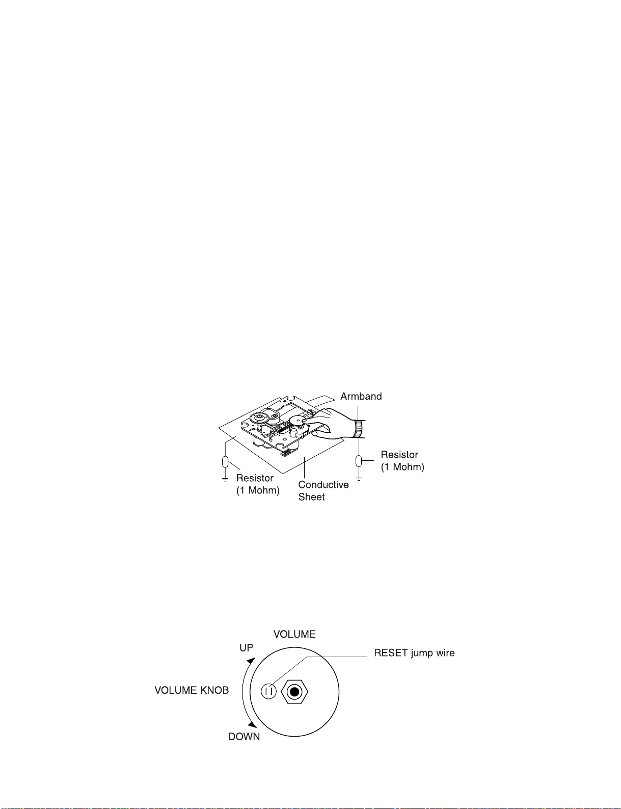
2.Notes for repair
1) Before replacing a component part, first disconnect the power supply lead wire from the unit
2) All equipment, measuring instruments and tools must be grounded.
3) The workbench should be covered with a conductive sheet and grounded.
When removing the laser pick-up from its conductive bag, do not place the pick-up on the bag. (This is
because there is the possibility of damage by static electricity.)
4) To prevent AC leakage, the metal part of the soldering iron should be grounded.
5) Workers should be grounded by an armband (1MΩ)
6) Care should be taken not to permit the laser pick-up to come in contact with clothing, in order to prevent
static electricity changes in the clothing to escape from the armband.
7) The laser beam from the pick-up should NEVER be directly facing the eyes or bare skin.
CLEARING MALFUNCTION
You can reset your unit to initial status if malfunction occur(button malfunction, display, etc.).
Using a pointed good conductor(such as driver), simply short the RESET jump wire on the inside of
the volume knob for more than 3 seconds.
If you reset your unit, you must reenter all its settings(stations, clock, timer)
NOTE: 1. To operate the RESET jump wire, pull the volume rotary knob and release it.
2. If you wish to operate the RESET jump wire, it is necessary to unplug the power cord.
Page 5
1-4
ESD PRECAUTIONS
Electrostatically Sensitive Devices (ESD)
Some semiconductor (solid state) devices can be damaged easily by static electricity. Such components
commonly are called electrostatically sensitive devices (ESD). Examples of typical ESD devices are
integrated circuits and some field-effect transistors and semiconductor chip components. The following
techniques should be used to help reduce the incidence of component damage caused by static electricity.
1. Immediately before handling any semiconductor component or semiconductor-equipped assembly, drain
off any electrostatic charge on your body by touching a know earth ground. Alternatively, obtain and
wear a commercially available discharging wrist strap device, which should be removed for potential
shock reasons prior to applying power to the unit under test.
2. After removing an electrical assembly equipped with ESD devices, place the assembly on a conductive
surface such as aluminum foil, to prevent electrostatic charge buildup or exposure of the assembly.
3. Use only a grounded-tip soldering iron to solder or unsolder ESD devices.
4. Use only an anti-static solder removal device. Some solder removal devices not classified as "anti-static"
can generate electrical charges sufficient to damage ESD devices.
5. Do not use freon-propelled chemicals These can generate electrical charges sufficient to damage ESD
devices.
6. Do not remove a replacement ESD device from its protective package until immediately before you are
ready to install it. (Most replacement ESD devices are packaged with leads electrically shorted together
by conductive foam, aluminum foil or comparable conductive materials).
7. Immediately before removing the protective material from the leads of a replacement ESD device, touch
the protective material to the chassis or circuit assembly into which the device will by installed.
CAUTION : BE SURE NO POWER IS APPLIED TO THE CHASSIS OR CIRCUIT, AND OBSERVE ALL
OTHER SAFETY PRECAUTIONS.
8. Minimize bodily motions when handing unpackaged replacement ESD devices. (Otherwise harmless
motion such as the brushing together of your clothes fabric or the lifting of your foot from a carpeted floor
can generate static electricity sufficient to damage an ESD device).
[CAUTION. GRAPHIC SYMBOLS]
THE LIGHTNING FLASH WITH ARROWHEAD SYMBOL. WITHIN AN EQUILATERAL
TRIANGLE, IS INTENDED TO ALERT THE SERVICE PERSONNEL TO THE PRESENCE
OF UNINSULATED "DANGEROUS VOLTAGE" THAT MAY BE OF SUFFICIENT
MAGNITUDE TO CONSTITUTE A RISK OF ELECTRIC SHOCK.
THE EXCLAMATION POINT WITHIN AN EQUILATERAL TRIANGLE IS INTENED TO
ALERT THE SERVICE PERSONNEL TO THE PRESENCE OF IMPORTANT SAFETY
INFORMATION IN SERVICE LITERATURE.
Page 6
1-5
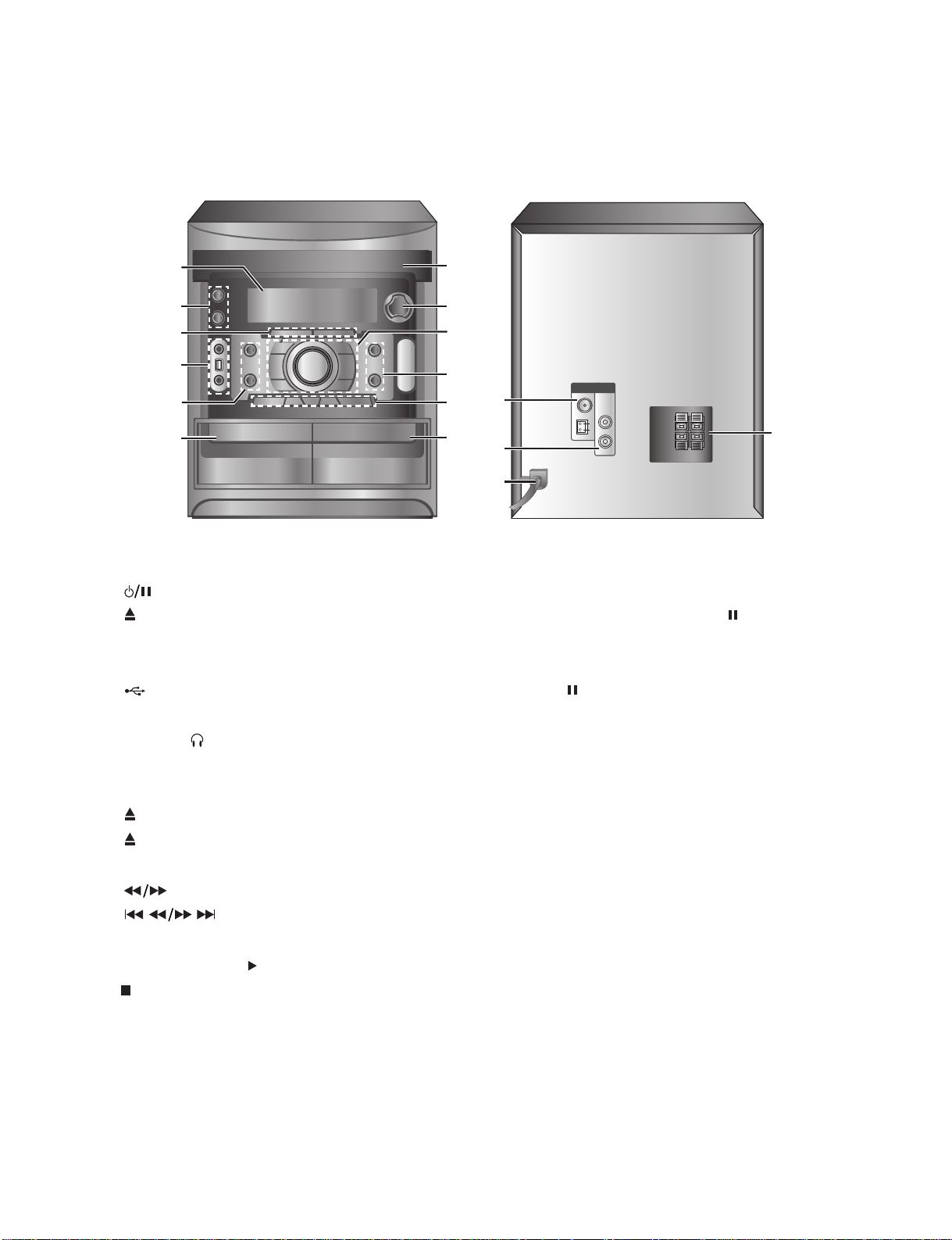
LOCATION OF USERS CONTROLS
FRONT / BACK PANEL
1. DISPLAY WINDOW
2. • (POWER) button
• OPEN/ CLOSE button
3. • XDSS/ MP3 OPT. button
• XTS - PRO button
4. • USB (OPTIONAL) / DEMO button
• USB connector (OPTIONAL)
• PHONES (HEADPHONE JACK) : ø3.5mm
5. • TUNER button
• AUX button
6. • PUSH EJECT position - TAPE 1
7. • PUSH EJECT position - TAPE 2
8. • TUNING (-/+) button
(REWIND / FAST FORWARD) button
(CD SKIP / SEARCH) buttons
• PRESET (-/+) button
FORWARD PLAY ( ) button
•STOP button
9. • CD button
• TAPE button
10.•CLOCK button
• TIMER button
• RDS(OPTIONAL) / SET / CD button
• EQ. button
• CD SYNC. / DUBB / ST./MONO button
• REC/
• VOLUME CONTROL KNOB
11.DISC SELECT buttons (DISC1, DISC2, DISC3)
12.DISC TRAY
13.AM/ FM ANTENNATERMINAL
14.AUX IN (AUXILIARY INPUT) connector
15.POWER CORD
16.SPEAKER TERMINAL
1
2
3
4
5
6
12
11
10
9
13
8
7
14
15
16
Page 7
1-6
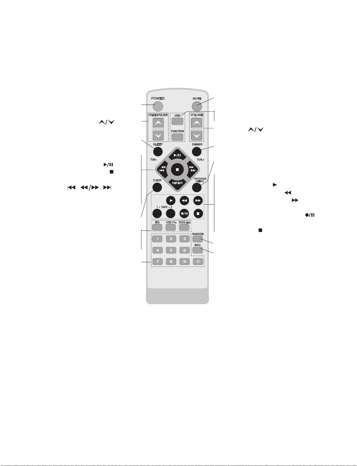
REMOTE CONTROL
POWER button
PRESET/FOLDER( ) buttons
SLEEP button
CD FUNCTION buttons
PLAY/PAUSE ( ) button •
CD STOP( ) button •
CD SKIP/ SEARCH •
() buttons
TUN.(-/+) buttons •
REPEAT button •
D.SKIP button
EQ (EQUALIZER PATTERN) button •
XTS Pro button •
XDSS plus button •
NUMERIC buttons
MUTE button
• USB (OPTIONAL) button
• FUNCTION button
VOLUME ( ) buttons
DIMMER button
PROGRAM/ MEMO button
TAPE FUNCTION buttons
• FORWARD PLAY ( ) button
• FAST REWIND PLAY ( ) button
• FAST FORWARD PLAY ( ) button
• TAPE-1/ 2 SELECT buttons
• RECORD/ RECORD PAUSE ( )
button
• TAPE STOP ( ) button
RANDOM button
INFO (MP3/ WMA file information
display) button
Page 8

1-7
SPECIFICATIONS
• GENERAL
Power supply Refer to the back panel of the unit.
Power consumption Refer to the back panel of the unit.
Net Weight 5.57kg (MCD202 Model)
5.36kg (MCD102 Model)
External dimensions (WxHxD) 273 x 371 x 326mm
• TUNER
FM Tuning Range 87.5 ~ 108.0MHz or 65 ~ 74MHz, 87.5 ~ 108.0MHz
Intermediate Frequency 10.7MHz
Signal to Noise Ratio 60/55dB
Frequency Response 50 ~ 10000Hz
AM Tuning Range 522 ~ 1620kHz or 520 ~ 1720kHz
Intermediate Frequency 450kHz
Signal to Noise Ratio 30dB
Frequency Response 140 ~ 1800Hz
• AMPLIFIER
Output Power 100W + 100W (MCD202 Model)
50W + 50W (MCD102 Model)
T.H.D 0.5%
Frequency Response 40 ~ 20000Hz
Signal-to-noise ratio 75dB
• CD
Frequency response 40 ~ 20000Hz
Signal-to-noise ratio 75dB
Dynamic range 75dB
• CASSETTE TAPE PLAYER
Tape Speed 3000 ± 3% (MTT-111. NORMAL-SPEED)
Wow Flutter 0.25% (MTT-111, JIS-WTD)
F.F/REW Time 120sec (C-60)
Frequency Response 250 ~ 8000Hz
Signal to Noise Ratio 43dB
Channel Separation 50dB (P/B) / 45dB (R/P)
Erase Ratio 55dB (MTT-5511)
• SPEAKERS
Speaker Name MCS202F MCS102F
Type Bass Reflex 2Way 2Speaker Bass Reflex 2Way 2Speaker
Impedance 4Ω 4Ω
Frequency Response 60 ~ 20000Hz 60 ~ 20000Hz
Sound Pressure Level 84dB/W (1m) 85dB/W (1m)
Rated Input Power 100W 50W
Max. Input Power 200W 100W
Net Dimensions (WxHxD) 220 x 342 x 270mm 200 x 337 x 228mm
Net Weight (1EA) 3.46kg 2.92kg
Page 9
I
J
D
H
A
B
E
B
M
N
N
C
F
G
A
J
K
H
L
L
K
M
I
C
G
E
F
D
A26
A41
A44
A40
A47
A46
266
263
305
A43
451
450
267
289
456
450
264
458
450
450
450
290
290
454
450
450
A00
257
255
255
256
259
253
282
253
254
450
CABLE2
CABLE4
CABLE3
CABLE1
CABLE5
CN201
CN806
P9701
P9702
260
CD
MAIN
SMPS
FRONT
291
2-1 2-2
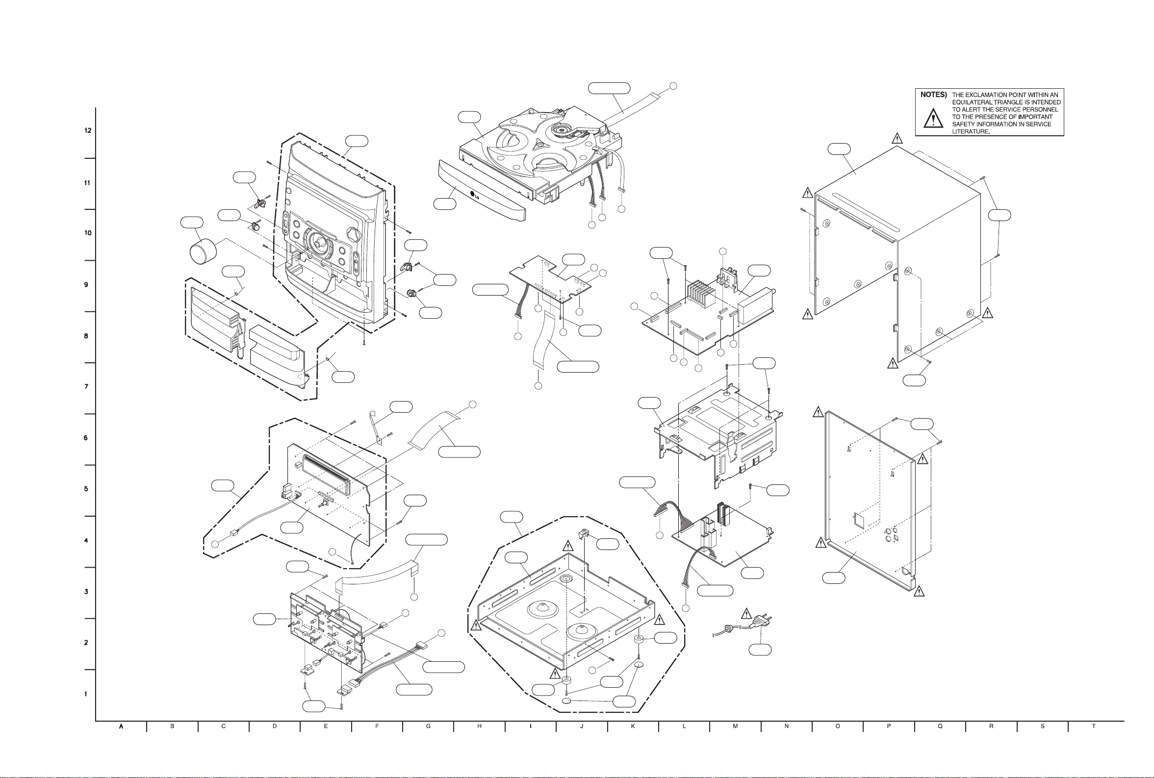
SECTION 2 EXPLODED VIEWS
CABINET EXPLODED VIEW
Page 10
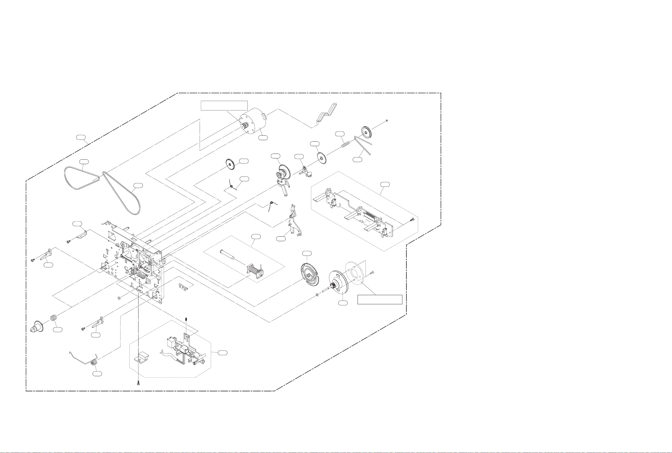
2-3 2-4
TAPE DECK MECHANISM EXPLODED VIEW
1. TAPE DECK MECHANISM (A/S & A/S : RIGHT A/S DECK)
BRASS MOTOR PULLEY MAYBE CHANGED
FOR WOW FLUTTER WHEN NECESSARY
009
003
A00
001
002
007
008
022
006
016
015
017
023
018
019
025
020
A01
RING FW MAYBE ADDED
FOR WOW FLUTTER WHEN NECESSARY
011
009
A02
013
Page 11

2-5 2-6
2. TAPE DECK MECHANISM (A/S & A/S : LEFT A/S DECK)
019
A00
003
009
007
008
016
017
022
018
023
015
020
RING FW MAYBE ADDED
FOR WOW FLUTTER WHEN NECESSARY
024
011
009
A03
013
Page 12
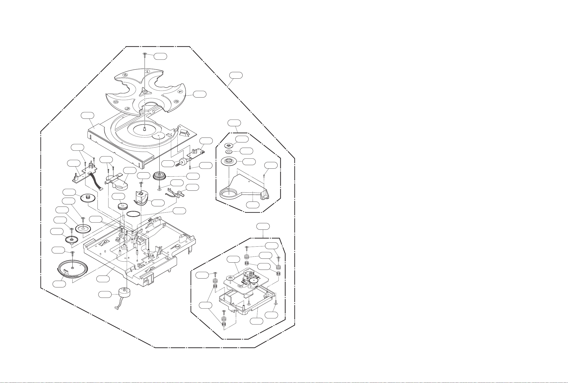
2-7 2-8
416
151
159
165
164
417
166
417
167
416
177
175
172
170
419
417
418
418
190
189
188
A30
A32
A26
181
187
186
184
421
421
185
156
155
153
173
168
163
162
441
440
422
A35
417
CD MECHANISM EXPLODED VIEW
Page 13
2-9 2-10
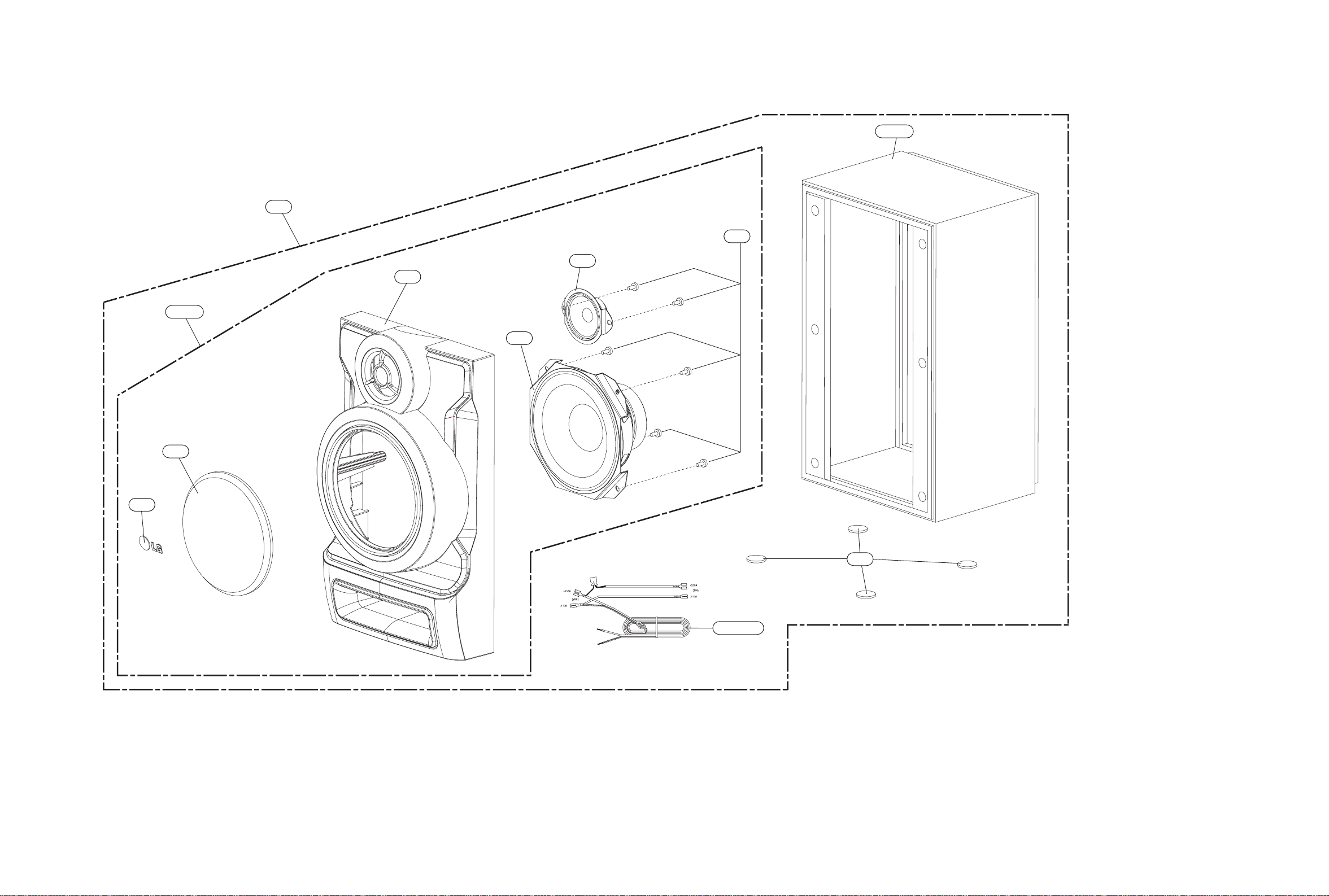
SPEAKER EXPLODED VIEW
MODEL : MCS102F
A80
A80A
A80B
855
853
850
854
852
851
856
WIRE80
Page 14

2-13
PACKING ACCESSORY VIEW
Page 15
3-1
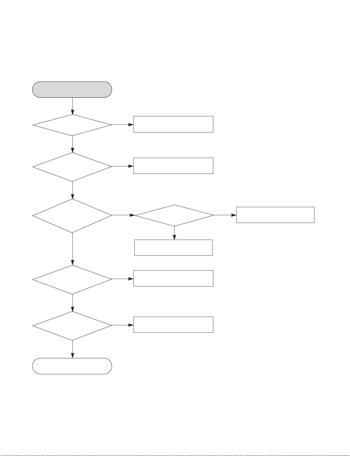
AUDIO ELECTRICAL TROUBLESHOOTING GUIDE
SECTION 3 AUDIO PART ELECTRICAL
1. POWER (SMPS)
POWER (SMPS)
OK
YES
YES
YES
Replace IC 901,902
Check IC901, 902
Check the fuse
F901
NONO
NO
YES
Check short of
P9701, P9702 line
Replace the fuse
Check
the DC V of C905.
If DC V is over
400V
NO
Check BD901, LF901, 902
Check the
DC V of C981, C945.
If DC V is 6.1V
NO
Check short of P9702 line
YES
YES
Chcek the
DC V of C950, C951
If DC V is in
31.5V
NO
Check short of P9701 line
Chcek the
DC V of C909, C903,
C921 If DC V is in 14~19V
and it is steady.
YES
Page 16
3-2
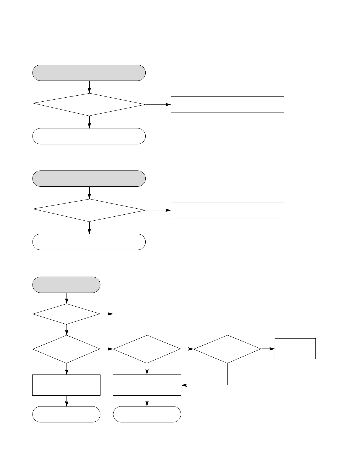
2. P-SENS
P-SENS
YES
YES
Check
the PIN6 of P9702
If DC V is over 5.6V
Check power circuit Trouble shooting
NO
OK
3. VKK CHECK
VKK check
YES
YES
Check
the PIN3 of P9702
If DC V is over -28V ±2
Check power circuit Trouble shooting
NO
OK
4. MICOM PART CHECK I
MICOM part check I
OK OK
YES
YES
Check P-SENS
(P7904)_PIN6.
NO
Refer to
SMPS troubleshooting.
YES
YES
YES
Check both
end voltage of IC101
(KIA7042).
Check
if input voltage of
IC101(KIA7042) is
over 5V.
YES
NO
Check the
periphery of IC101
(KIA7042).
NO
YES
Check if IC101(KIA7042) of
output voltage is over 4.3V.
Check voltage of IC100
78KO/KF2_PIN1.
NO
Replace IC101
(KIA7042).
Page 17
3-3
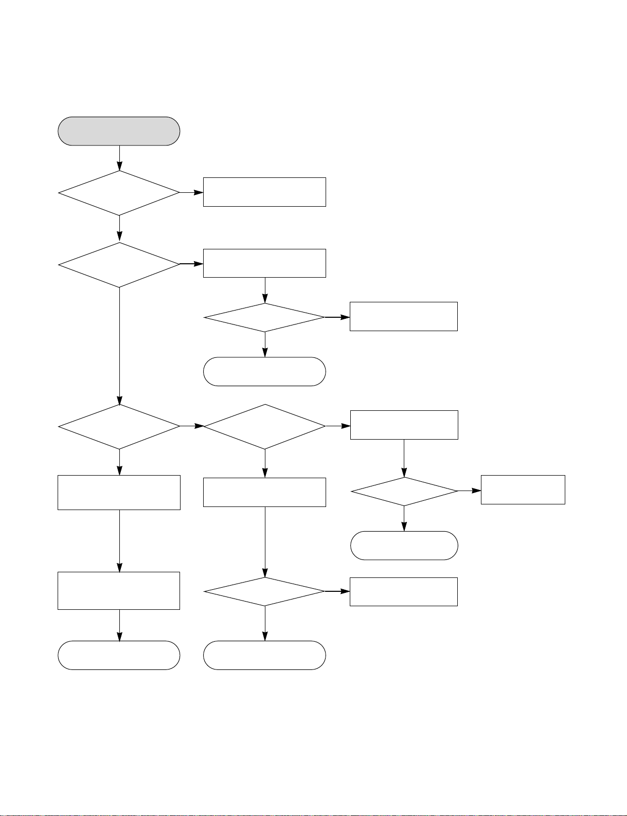
5. MICOM PART CHECK II
MICOM part check II
X101 : 32.768kHz
X100 : 9.8304MHz
Check the operation.
Check
Q101_ emitter/collector
5V.
Check Q102_base
0.6V HIGH.
Check if IC103_PIN8 and
IC100_PIN19, 20, 59 are 5V.
NO NO
YES
YES
Check if
voltage of P7904_PIN5
is 5.6V.
NO
Refer to
SMPS troubleshooting.
YES
YES
YES
OK
YES
Check
both end voltage of
D101
YES
YES
Check D101.
NO
Check if output of
D101(1SR35) is 5V.
YES
YES
YES
YES
Check IC101.
Q102_collector 0.6V LOW.
OK
Check if output of IC101
(KIA7042) is over 4.3V.
OK
NO
Replace IC101.
NO
Replace D101.
YES
Check Q102.
OK
NO
Replace Q102.
Page 18

3-4
Check
IC100(78KOKF2)_
PIN 22, 24
OK
YES
YES
Refer to
micom troubleshooting
Check micom
voltage 5V.
PIN22
DATA PIN24 CLK
NONO
YES
Replace micom.
Check micom.
NO
YES
OK
6. IC103(KS4CD21CS) CHECK
Page 19

3-5
FLD display check
YES
YES
Replace P3702.
Check each
PIN voltage.
NO
NO
YES
YES
OK
Replace IC301.
Check IC301.
NO
YES
Replace IC100FLD light on?
Check IC100.
NO
YES
YES
OK
Refer to SMPS
7. FLD DISPLAY CHECK
YES
YES
Check
P7904_PIN1, 2, 3 voltage
input.
NO
Check P3702 connection.
NO
If voltage is not 5V,
check input and output
of D319(1SR35).
YES
Check P3702
connection and power.
Pin1 : FL-22 Pin2 : FL+26
Pin3 : VKK- over
26V.
YES
YES
YES
YES
OKOK
76 PIN - > DO - - >
Check DATA in Check IC100.
NO
IC100
75 PIN - > STB
77 PIN - > 4PIN DI
78 PIN - > 1PIN CLK
Check data output.
IC100 - >
Check IC301
DATA communication.
PIN PIN
75PIN - > 3PIN STB
76PIN - > 2PIN D
78PIN - > 1PIN
CLK
Check
IC301(PT6324) voltage.
Pin50 VKK : -26V
PIN9.52 : +5V
Check if both end votage
of F1, F2 are over 3.7V.
VKK : over 26V.
Page 20

3-6
8. PWM MODULATION PART CHECK
PWM modulation
part check
YES
YES
YES
YES
P7905_PIN9
3.3V checking
Check IC604(PS9829)
VDD PIN voltage(3, 7, 8,
10, 22, 29, 39, 47, 56, 65,
72, 94).
Check X601_PIN2 3.3V.
NO
Refer to
SMPS troubleshooting.
YES
YES
YES
YES
Check IC605_
PIN3 input and PIN2
output.
Check
X601 12.288MHz
operation.
Check IC605_
PIN8 3.3V.
Check IC605_
PIN3 input
Check X601
2.288MHz
NO
NO
IC604
(PS9829) PIN86 CLK
input check
NO
Check FB614
BEAD input, output and
voltage.
NO
Check X601
12.288MHz.
Replace X601.
OK
NO
OK
YES
YES
NO
Replace FB614
NO
Check IC605_
PIN2 output
YES
OK
YES
OK
Replace IC605.
NO
Check R680
(470Ω) output.
Replace R680.
NO
Check
IC604(PS9829) DATA
input.
Check each LINE
registor output.
NO
Check IC604
(PS9829) DATA input.
78 PIN->DATA
79 PIN->CLK
Check PWM
modulator output.
FL:75(+)74(-)
FR:71(+)70(-)
NO
NO
Check
DVD ASS`Y(PS9829)
communication
(P7403).
Refer to
CD troubleshooting.
NO
Check
IC100(78KOKF2)
21->PWM_CLK
22->PWM_DATA
43->PWM_REST
output.
NO
YES
YES
OK
YES
OK
Check IC604(PS9829).OK
Check
LINE registor output.
DATA:R671, CLK:R670
RST:R665
Replace R670, R671
and R665
NO
NO
Replace X601.
OK
YES
YES
YES
YES
Page 21

3-7
Power AMP part check
YES
Check each LINE registor output voltage.
IC700 : R701, 702, 726, 727
NO
Check each
IC700, 701, 702, 703
PIN1,17, 18, 19, 36 +12V
input.
Refer to SMPS troubleshooting.
YES
YES
YES
NO
P7905_3PIN : +12V,
PIN13, 14, 15 : 35V.
YES
Replace the coils
YES
NO
Check output line coil.
Check PWM modulator input.
Each IC PIN4, 6, 14, 16
YES
Power IC700, 701, 702, 703
PIN20, 27, 29, 34 output.
Check each IC700, 701, 702, 703
PIN21, 26, 29, 34 input voltage.
OK
9. POWER AMP PART CHECK
Page 22

3-8
10. AUX FUNCTION CHECK
AUX function check
Check µ-COM(IC301)_
PIN83, 84 commucation.
NO
NO
YES
Replace IC200
YES
YES
YES
Check
IC200(BU4052)_
PIN4, 11 input
waveform.
Check
IC200(BU4052)_PIN16
VDD, PIN8 VSS
power.
Refer to
SMPS troubleshooting.
NO
NO
YES
Replace IC801OK
YES
YES
Check
IC801(MC4580)_PIN 2, 6
input waveform.
Check
IC801(MC4580)_PIN4
VSS, PIN8 VDD
power.
Check IC200(BU4052)_
PIN3, 13 output waveform.
Check JK800 connection.
Page 23

3-9
11. TUNER FUNCTION CHECK
TUNER function check
YES
Check IC200(BU4052)_
PIN16 VDD, PIN8 VSS power.
NO
Check
IC200(BU4052)_PIN3, 13
output waveform and IC601
(BU4052)_PIN2,15 input
waveform.
Check TUNER module voltage(PIN2 : 9V).
YES
YES
YES
YES
NO
Check TUNER
module(TU601) operation.
YES
Check IC801(MC4580)_
PIN4 VSS, PIN8 VDD power.
YES
NO
Check IC801(MC4580)_
PIN2, 6 input waveform.
Replace IC200.
Replace IC200.
Replace IC801.
Check IC200(BU4052)_PIN1, 12 input
waveform.
OK
Page 24

3-10
12. TAPE FUNCTION CHECK
TAPE function check
YES
Check IC200(BU4052)_
PIN16 VDD, PIN8 VSS power
YES
YES
YES
NO
Check
IC200(BU4052)_PIN2, 15 input
waveform.
Check IC200(BU4052)_
PIN16 VDD, PIN8 VSS power
YES
NO
Check IC801(MC4580)_
PIN2, 6 input waveform.
YES
Replace IC200.
Replace IC200.
Replace IC200.
Check IC200(BU4052)_PIN3, 13
output waveform and IC601(BU4052)_
PIN2, 15 input waveform.
YES
TAPE PCB ASS`Y
OK
Page 25

3-11
13. TAPE PLAY PART CHECK
TAPE PALY part check
Replace head wire and tape
deck mechanism.
NO
NO
YES
YES
Check Adeck head input
IC201_PIN32, 39 and B deck
head input IC201_PIN34, 37.
YES
YES
YES
YES
Check IC201_
PIN5, 26 signal
output.
Check
IC201(HA12237)_PIN16
12V input.
Check A/B
deck head input.
NO
Refer to
SMPS troubleshooting.
Check IC202_PIN10 "HIGH"
NO
Check IC201_PIN14
mute operation.
Replace IC201.
NO
YES
OK
Check IC201
YES
Replace IC202.
NO
YES
OKOK
Check IC202.
Page 26

3-12
14. TAPE REC PART CHECK
TAPE REC part check
Check IC100_PIN23 "HIGH"
NO
NO
YES
YES
Check IC201_
PIN7, 24 record input.
Check P2203_PIN5, 3 input
and PIN8 erase input.
YES
YES
YES
YES
YES
Check L203_PIN2, 3
oscillation.
Check
IC604(PS9829)_PIN49, 52
PWM output.
Check Q205(D1304)_
base "HIGH".
Replace IC201.
NO
NO
Check IC201_
PIN10, 21 output.
Check IC100_PIN23
"HIGH"
NO
Refer to PWM
modulation troubleshooting.
OK
YES
Replace IC202.
YES
OK
OK
Page 27

3-13
INTERNAL BLOCK DIAGRAM OF ICs
1.ES6838
GPIO
SDRAM/ROM
Interface
Audio ADC
Serial Audio
Interface
Audio DAC
USB
DVD
Descrambler
Transport
ATAPI
32-Bit
RISC
Processor
16 K Cache
Gateway
+
DMA
Controller
Huffman
Decoder
+
Servo Controller / RF
Video
Processor
Display
OSD / SPU
Controller
Scaler
DeIntelacer
TV-Encoder
VDAC
HDMI I/F
8051
µController
DSC
Digital
PLL
ROM
RAM
DRAM
Interface
ECC
Page 28

3-14
2.HA12237F
Page 29
3-15
3.PS9829B
/
4.PT6324
MBCK
MLRCK
MSDIN[0:3]
SBCK
SLRCK
SSDIN[0:3]
MIC_MCLK
MIC_BCK
MIC_LRCK
MIC_SDIN
SPI/I2C
SO/SDA
SCK/SCL
SI/I2C_AD0
CS/I2C_AD2
EXT_MUTE
Input
&
Output
MUX
Sample
Rate
Converter
Input
Mapper
Mic,
Input
Processor
Host
Interface
2
C, SPI)
(I
Internal Controls
Down
Mixer
Mixer
Serial Audio
Output
Interface
4 Band
EQ
Internal Clock Internal Reset
Manager
Reset & Power Down
PLL
Bass
Automatic
Gain
Limiter
Main
Volume
Power Supply
Trim
Volume
Serial
Audio
Output
Interface
Output Mapper
PWM
Modulator
POP
NR
DMIX_MCLK
OLRCK
OBCK
DMIX_SDOUT
PWM1_P/M
PWM2_P/M
PWM3_P/M
PWM4_P/M
PWM5_P/M
PWM6_P/M
PWM7_P/M
PWM8_P/M
PWM_HP_L_P/M
PWM_HP_R_P/M
PWM_SWL_P/M
EPD_ENA
OVERLOAD
DIN/DOUT
CLK
STB
OSC
LED1
Serial
Data
Interface
CSC
LED
Driver
CLK_IN
Control
Display Memory
Timing Generator
Key Matrix Memory
/RESET
PLL_AVDD
PLL_DVSS
PLL_DVDD
Dimming Circuit
DVDD
PLL_AVSS
DVSS
IO_VSS
IO_VDD
Segment Driver
Grid
Driver
SG1/KS1
SG2/KS2
SG3/KS3
SG4/KS4
SG5/KS5
SG6/KS6
SG7/KS7
SG7/KS7
SG8/KS8
SG9/KS9
SG10/KS10
SG11/KS11
SG12/KS12
SG13/KS13
SG14/KS14
SG15KS15
SG16/KS16
SG17
SG18
SG19
SG20
SG21
SG22
SG23
SG24
GR1
GR2
GR3
GR4
GR5
GR6
GR7
GR8
GR9
GR10
GR11
GR12
GR13
GR14
GR15
GR16
K1 K2 VDD GND VEE
Page 30

3-16
5.STR-S6757IF1905
4
Vcc
Reg&
Iconst
Burst
Control
S
OVP
Start
Stop
Burst
RQ
OSC
Protection
latch
R
Q
S
Q
DRIVE
Reg
Delay
S
R
OCP
FB
D
S
GND
FB
1
2
3
6
OLP
Soft Start
MaxON
Bottom Selector
BSD
Counter
BD
OCP/BD
7
SS/OLP
5
Page 31

3-17
6. TAS5142
System
Microcontroller
T
AS5508
V
ALID
OTW
SD
RESET_AB
RESET_CD
SD
OTW
BST_A
BST_B
Bootstrap
Capacitors
Left-
Channel
Output
Right-
Channel
Output
System
Power
Supply
32 V
Hardwire
Mode
Control
PVDD
PWM_A
PWM_B
PWM_C
PWM_D
M1
M2
M3
Input
HúBridge 1
Input
H-Bridge 2
PVDD_A, B, C, D
GND_A, B, C, D
4
4 4
PVDD
Power
Supply
Decoupling
2-Channel
H-Bridge
BTL Mode
GVDD_A, B, C, D
VDD
GND
VREG
GVDD
VDD
VREG
Power Supply
Decoupling
Output
H-Bridge 1
Output
H-Bridge 2
AGND
OC_ADJ
Hardwire
OC Limit
OUT_A
OUT_B
OUT_C
OUT_D
BST_C
BST_D
2nd-Order L-C
Output Filter
for Each
Half-Bridge
2nd-Order L-C
Output Filter
for Each
Half-Bridge
Bootstrap
Capacitors
VAC
GND
12 V
GND
GVDD (12 V)/VDD (12 V)
Page 32
3-18
7. U1739EJ2V1UD00/KF2_E
TO00/TI010/P01
TI000/P00
RxD6/P14 (LINSEL)
TO01/TI011/P06
TI001/P05
TOH0/P15
TOH1/P16
TI50/TO50/P17
TI51/TO51/P33
RxD0/P11
TxD0/P10
RxD6/P14
TxD6/P13
SI10/P11
SO10/P12
SCK10/P10
SI11/P03
SO11/P02
SCK11/P04
SCK11/P05
SIA0/P143
SOA0/P144
SCKA0/P142
STB0/P145
BUSY0/P141
EXSCL0/P62
SDA0/P61
SCL0/P60
ANI0/P20 to
ANI7/P27
AV
REF
AV
SS
RxD6/P14 (LINSEL)
INTP0/P120
INTP1/P30 to
INTP4/P33
INTP5/P16
INTP6/P140,
INTP7/P141
16-bit timer/
event counter 00
16-bit timer/
event counter 01
8-bit timer H0
8-bit timer H1
Internal low-speed
Watchdog timer
8-bit timer
event counter 50
8-bit timer
event counter 51
Serial
interface UART0
Serial
interface UART6
Serial
interface CSI10
Serial
interface CSI11
Serial
interface CSIA0
Serial
interface IIC0
8
A/D converter
4
2
oscillator
Watch timer
LINSEL
Interrupt
control
78K/0
CPU
core
Note 1
BANK
Internal
high-speed
RAM
VDD,
EVDD
VSS,
EVSS
Flash
memory
Internal
expansion
RAM
FLMD0
Port 0 P00 to P06
Port 1 P10 to P17
Port 2 P20 to P27
Port 3 P30 to P33
Port 4 P40 to P47
Port 5 P50 to P57
Port 6 P60 to P67
Port 7 P70 to P77
Port 12 P120 to P124
Port 13
7
8
7
4
8
8
8
8
5
P130
Port 14 P140 to P1456
Buzzer output
Clock output
control
Power on clear/
low voltage
indicator
Key return
POC/LVI
8
BUZ/P141
PCL/P140
control
Reset control
Multiplier &
divider
On-chip debug
System
control
Note 2
OCD0A
OCD0B
RESET
XT1/P121
X2/EXCLK/P122
XT1/P123
XT2/EXCLKS/P124
Internal high-speed
oscillator
Voltage
regulator
KR0/P70 to
KR7/P77
Note 2
Note 2
REGC
/X1, OCD1A
/X2, OCD1B
EXLVI/P120
Note 2
/P31
Note 2
/P32
Page 33

3-20
3-21
WIRING DIAGRAM
SMPS PCB
15P
2 CH SPK TERMINAL
3 CHANGER MD
3P
RED
5P
6P
RED
AUX
JACK
MODULE
TUNER
[Total CNT Q'ty : 14ea]
1. SMPS MAIN : 2ea
2. MAIN DVD : 2ea
3. MAIN FRONT : 1ea
4. FRONT DVD : 1ea
5. DVD MD : 5ea
6. DECK MECHA. : 3ea
4P
4P
CD PCB
30P
USB MIC H/P
8P3P 13P
MAIN
PCB
29P
DOUBLE DECK
MECHANISM
FRONT PCB
Page 34

3-22 3-23
BLOCK DIAGRAMS
1. SMPS BLOCK DIAGRAM
RECTIFICATION
SMOOTHING
AMP
Switch
T
R
A
CIRCUIT
ZNR &
FILTER
AC INPUT
IC #
MAIN
Switch
IC #
1
2
N
S
#1
T
R
A
N
AMP (+) 31 .5V
FEED BACK
3.5V (278R35)
6.1V (KIA278R05)
P9701
12V (78R12)
5V(P-SENS)
P9702
S
#2
-12V
-31. 5V(VKK)
FL1-FL2 (4.5V)
FEED BACK
Page 35

3-24 3-25
2. MAIN & FRONT BLOCK DIAGRAM
DECK B
DECK A
DECK S/W
TUNER MODULE
AUX
L/R, REC_L/R
ERASE
L/R
TUNER_L / R
AUX_L / R
[5]
BU4052
AUDIO
S/W
HA12237F
Cassette
Deck
AS
P
DECK_L / R
AUDIO L / R
REC_MUTE, PB_MUTE, TAPE_A/B
[4]
SOL_A/B, MOTOR, REC_BIAS
[4]
HALL_A/B, LEAF_A/B
[4]
RDS_CLK / DATA, PLL_DO / CLK / CE[5]
PLL_DI, T_MUT
AK5358
2CH.
ADC
E[2]
4052_A / B
MCLK, LRCK, BCK, SD_OUT [7
TR DRIVER
KS24C021
EEPROM
VFD_STB / DI / DO / CL
ADC_RS
T
EEPROM
CLK/DATA
[4]
K
]
9.8304MHz
78F0546
AUDIO
MICOM
TX
RX
9830_RST
CLK/DAT
[3]
A
PS9830
Modulato
REC_L / R
H/P_L / R
CLK,DATA
FSEQ,WRQ,CD_DO,RX [4]
EIGHT KINDS EXCEPT CD IN
74HCT244
BUFFER
12.288MHz
PWM
5142_RST
5142_S
D
FL +/-
FR +/-
SW +/
r
LRCK,BCK,DATA0
TAS5152
FL
or
TAS5142
-
Digital
Power
AM
P
[3]
FR
SW
AUX2
H/P
MIC
USB
AUX2 _L/R
MIC _SIG
BA3308
OPAMP
(ALC)
FSEQ,WRQ,CD_DO
PT6324
MIC _SIG
FLT
DRIVER
CLK,DATA,+5V,GND
CY8C21484
TOUCHPAD
DRIVER IC
[4]
TX, RX
16.9344MHz
14.3178MHz
LC78692W
DSP IC
FDO,TDO
SLDO,SPDO
[4]
[4]
A,B,C,D,E,F
AM5810
MOTOR
DRIVER
TA+/-,
FA+/-
SL+/-, SP+/-
/CL
OP
[4]
[4]
PICK UP
PICK UP
MOTOR
MOTOR
TOUC
FLT
DISPLAY
H PAD
D+ / D-,+5V/G
ND
OTI6888
[4]
VER.A
MD
STDATA, STCK, STREQ[3]
MD
9
Page 36

3-26 3-27
SCHEMATIC DIAGRAMS
1. SMPS SCHEMATIC DIAGRAM
WHEN SERVICING THIS CHASSIS, UNDER NO
CIRCUMSTANCES SHOULD THE ORIGINAL DESIGN
BE MODIFIED OR ALTERED WITHOUT PERMISSION
FROM THE LG CORPORATION. ALL COMPONENTS
SHOULD BE REPLACED ONLY WITH TYPES
IDENTICAL TO THOSE IN THE ORIGINAL CIRCUIT.
SPECIAL COMPONENTS ARE SHADED ON THE
SCHEMATIC FOR EASY IDENTIFICATION. THIS
CIRCUIT DIAGRAM MAY OCCASIONALLY DIFFER
FROM THE ACTUAL CIRCUIT USED. THIS WAY,
IMPLEMENTATION OF THE LATEST SAFETY AND
PERFORMANCE IMPROVEMENT CHANGES INTO
THE SET IS NOT DELAYED UNTILTHE NEW SERVICE
LITERATURE IS PRINTED.
1. Shaded( ) parts are critical for safety. Replace only
with specified part number.
2. Voltages are DC-measured with a digital voltmeter
during Play mode.
IMPORTANT SAFETY NOTE :
Page 37

3-28 3-29
2. MAIN SCHEMATIC DIAGRAM
Page 38

3-30 3-31
3. AMP SCHEMATIC DIAGRAM
Page 39

3-32 3-33
4. DECK SCHEMATIC DIAGRAM
Page 40

3-34 3-35
5. FRONT SCHEMATIC DIAGRAM
Page 41

4-1
CD ELECTRICAL TROUBLESHOOTING GUIDE
1. CD PART TROUBLESHOOTING
Turn on CD
YES
YES
NO
OPEN CLOSE check
Connector check (PN803, PN804)
NO
Check voltage CN806
PIN1 : 12, PIN2 : 6.3V
NO
Check voltage PN805
PIN22 : CLOSE, PIN23 : OPEN
YES
NO
“Reading”
Display check
Connector check
(PN802, PN803, PN804, CN806, PN814)
NO
Check micom interface circuit (PN805)
(CE, BTL-MUTE, CD-IN, CD-OUT, CLK, WRQ, FSEQ)
YES
NO
Reading OK check
Connector check (PN801,PN802)
NO
YES
If PALY, AUDIO
OUTPUT check
Check PN805 audio data
PIN10 : DA_LRCK (IC801 PIN60 LRSY)
PIN11 : DA_BCK (IC801 PIN59 DATACLK)
PIN12 : DA_DATA0 (IC801 PIN58 DATA)
NO
Check pick up movement
NO
Check AM5810FP (IC802)
NO
Check LC78692 (IC801)
OK
SECTION 4 CD PART ELECTRICAL
Page 42

4-2
1-1. OPEN CLOSE NG
Connector locking check
(PN803, PN804, PN814)
YES
YES
YES
YES
Check power
supply circuit (PN805, CN806)
CN806 PIN1 : 12V, PIN2 : 6.3V
PN805 PIN8 : +5V_AD
Defective main power supply
NO
Check voltage change LO+, LO- OF IC803
(PN805 PIN23 : OPEN, PIN22 : CLOSE)
Defective IC803
Defective mechanism
NO
Check voltage
change of OPEN CLOSE
IC803 INPUT voltage PIN6 : 12V,
PIN7:6.3V (PN805 PIN2 :
BTL_MUTE, 23 : OPEN,
22 : CLOSE)
Defective micom
NO
Page 43

4-3
1-2. “READING” DISPLAY CHECK (= ONLY “CD” DISPLAY)
Conector locking check
(PN802, PN803, PN804, PN805, CN806)
YES
YES
YES
YES
YES
Check power
supply port (PN805, CN806)
CN806 PIN1 : 12V, PIN2 : 6.3V,
PIN4 : 5V PN805
PIN8 = 5V_AD
Defective connector or main power supply
Defective IC804
NO
Check micom interface circuit (PN805)
PN805 PIN1, 3, 4, 15, 19, 26 signal check
(1 : CE, 3 : DI, 4 : CLK, 15 : D0, 19 : RST,
18 : FSEQ, 26 : WRQ) PIN3 DI : From DSP
to micom PIN15 DO : From micom to DSP
Check the waveform #1
Defective micom or connector
Defective IC801
NO
Check voltage
The PIN2 of IC804
IC804 PIN2 : 3.3V
NO
Defective micom or connector
Check reset
signal of PN805
PN805 PIN19 : 5V
NO
Page 44

4-4
Connector locking check
(PN801, PN802)
Is reading OK?
Defective pick up or
IC802 or IC801
Does sled move?
NO
NO
Check PN802
PIN3, 4 (SL+, SL-)
1-3. READING OK CHECK (= “NO DISC” DISPLAY)
Does lense move?
(= UP & DOWN)
YES
A
YES
Defective pick up or
IC802 or IC801
NO
NO
Check PN801
PIN13, 16 (FA+, FA-)
B
Defective pick up or IC801
Does laser light?
NO
NO
Check PN801 PIN10 (LD)
YES
C
Defective pick up or
IC802 or IC801
Does spindle rotate?
NO
NO
Check PN802
PIN5, 6 (SP+, SP-)
YES
D
Defective pick up or
IC802 or IC801
NO
NO
Check PN801
PIN14, 15 (TA+, TA-)
E
Page 45
4-5
Defective IC801
Does
SL+ waveform
appear at (IC802 PIN13
and PN802 PIN3)
waveform #2
sled motor
wave
Does slin
waveform appear at
(IC802 PIN5)
waveform #2
sled drive
wave
NO
NO
1-4. READING OK CHECK #A (= “NO DISC” DISPLAY)
YES
YES
A
Defective IC802
NO
Defective PN802 connector
Defective pick up sled motor
Check PN802 connector line
YES
Defective IC801
Does
FA+ waveform
appear at (IC802 PIN16
and PN801 PIN13)
waveform #3 focus
coil drive
wave
Does
fain-waveform
appear at (IC802 PIN25)
waveform #3
focus drive
wave
NO
NO
1-5. READING OK CHECK #B (= “NO DISC” DISPLAY)
YES
YES
B
Defective IC802
NO
Defective PN801 connector
Defective pick up
focus actuator
Check PN801 connector line
YES
Page 46

4-6
Defective IC804
Is ?V applied
to PIN10 of PN801
laser supply voltage
check
Is 3.3V
applied to
PIN30, 36, 39, 41, 61,
68, 75 of IC801 RF IC
supply voltage
check
NO
NO
1-6. READING OK CHECK #C (= “NO DISC” DISPLAY)
YES
YES
Defective IC801
Is 2.3V
PIN18 (LDO) of IC801
laser control voltage
check
NO
YES
C
Defective Q801 or D801
NO
Defective PN801 connector
Defective pick up laser part
Check PN801 connector line
YES
Page 47

4-7
Defective IC801
Does
SP+ waveform
appear at (IC802
PIN11 and PN802 PIN5)
waveform #4 spindle
motor drive
wave
Does
spin waveform
appear at (IC802 PIN6)
waveform #4
spindle drive
wave
NO
NO
1-7. READING OK CHECK #D (= “NO DISC” DISPLAY)
YES
YES
D
Defective IC802
NO
Defective PN802 connector
Defective pick up
spindle motor
Check PN802 connector line
YES
Page 48

4-8
Does FE, TE signal
appear? (IC801
PIN10 : RFMON, PIN16 : TE)
waveform #6
* REMON is FE
Defective IC801
Does
TA+ waveform
appear at (IC802 PIN17
and PN801 PIN14)
waveform #5 tracking
coil drive
wave
Does
tain - waveform
appear at (IC802 PIN22)
waveform #5
tracking drive
wave
NO
NO
1-8. READING OK CHECK #E (= “NO DISC” DISPLAY)
YES
YES
E
Defective IC802
Does
ARF signal appear?
(IC801 PIN 2)
waveform #6
NO
Defective pick up or IC801
Check PN802
connector line
NO
Defective PN802 connector
YES
YES
NO
Defective pick up or IC801
Page 49

4-9
2. USB PART TROUBLESHOOTING
Turn on USB
YES
NO
YES
Connector check
(PN805, CN806, PN810 )
NO
Check power supply circuit (CN806)
Check micom interface circuit (PN805)
PIN13 : RX (IC805 PIN49 : TXD)
PIN14 : TX (IC805 PIN33 : RXD)
NO
NO
Check PN810 PIN2(D-), 3(D+)
Check OTI6888 (IC805)
Connector check (CN806)OK
YES
“Checking” or
“USB” display check
NO
YES
Check PN810 1PIN : 5V
Reading OK check
NO
Check signal STCK, STREQ, STDATA
STCK : IC805 PIN52, IC801 PIN55
STREQ : IC805 PIN53, IC801 PIN54
STDATA : IC805 PIN54, IC801 PIN56
If PLAY, AUDIO
OUTPUT check
NO
NO
Page 50

4-10
WAVEFORMS OF MAJOR CHECK POINT
#1.MICOM INTERFACE WAVEFORM
(PN805 PIN26, 19, 3, 15) during power on
PIN26 : WRQ
PIN19 : RESET
PIN3 : DI (IC801 PIN46 DATA OUT)
PIN15 : DO (IC801 PIN45 DATA IN)
#1.MICOM INTERFACE WAVEFORM
(PN805 PIN26, 19, 3, 15) during normal play
PIN26 : WRQ
PIN19 : RESET
PIN3 : DI (IC801 PIN46 DATA OUT)
PIN15 : DO (IC801 PIN45 DATA IN)
#1.MICOM INTERFACE WAVEFORM
(PN805 PIN4, 1, 18) during power on
PIN4 : CL
PIN1 : CE
PIN18 : FSEQ
#1.MICOM INTERFACE WAVEFORM
(PN805 PIN4, 1, 18) during normal play
PIN4 : CL
PIN1 : CE
PIN18 : FSEQ
Page 51

4-11
#2.SLED DRIVE AND MOTOR WAVEFORM
(IC802 PIN5, 13) when focus search
PIN5 : SLIN
PIN13 : SL+
#2.SLED DRIVE AND MOTOR WAVEFORM
(IC802 PIN5, 13) during normal play
PIN5 : SLIN
PIN13 : SL+
#3.FOCUS DRIVE AND MOTOR WAVEFORM
(IC802 PIN25, IC802 PIN16)
• When focus search failed or there is no
disc on tray
PIN25 : FAO
PIN16 : FA+
#3.FOCUS DRIVE AND MOTOR WAVEFORM
(IC802 PIN25, IC802 PIN16)
• There is disc on tray and focus search success
PIN25 : FAO
PIN16 : FA+
Page 52

4-12
#4.SPINDLE DRIVE AND MOTOR WAVEFORM
(IC802 PIN6, 11) when TOC reading
PIN6 : SPIN
PIN11 : SP+
#5.TRACK DRIVE AND MOTOR WAVEFORM
(IC802 PIN22, IC802 PIN17) during normal play
#6.RF, FOCUS AND TRACKING ERROR WAVEFORM
(IC801 PIN2, 10, 16) during normal play
PIN2 : RFOUT
PIN 16 : TE
PIN10 : RFMON(FE)
PIN22 : TAO
PIN17 : TA+
Page 53

4-13 4-14
SCHEMATIC DIAGRAMS
1. CD SCHEMATIC DIAGRAM
Page 54

4-15 4-16
2. USB SCHEMATIC DIAGRAM
 Loading...