

LG M4200N, M4200N-B10C.AHLF, M4200N-B10C.AHXF Service Manual
COLOR MONIT OR
SER VICE MANUAL
Website:http://biz.LGservice.com
E-mail:http://www.LGEservice.com/techsup.html
CAUTION
BEFORE SERVICING THE UNIT,
READ THE SAFETY PRECAUTIONS IN THIS MANUAL.
CHASSIS NO. : LW52A
MODEL: M4200N (M4200N-B10C.AH**XF, AH**LF)
( ) **Same model for Service
- 2 -
1. LCD CHARACTERISTICS
Type : TFT Color LCD Module
Active Display Area :
42.02inches(1067.308mm) diagonal
Pixel Pitch : 0.227mm x 0.681m x RGB
Color Depth : 8-bit, 16,777,216 colors
Electrical Interface : LVDS
Size : 1006mm(H) x 610(V)x59(D)mm
Surface Treatment : Anti-Glare, Hard Coating(3H)
Operating Mode : Normally Black
Backlight Unit : 20-CCFL(20 lamps)
2. OPTICAL CHARACTERISTICS
2-1. Viewing Angle by Contrast Ratio ≥ 10
Left : -85° min., -89°(Typ.) Right : +85° min., +89°(Typ.)
Top : +85° min., +89°(Typ.) Bottom : -85° min., -89°(Typ.)
2-2. Luminance : 400(min), 500(Typ.)
2-3. Contrast Ratio : 400(min), 550(Typ.) (Without AI)
800(min), 1100(Typ.) (With AI)
3. SIGNAL (Refer to the Timing Chart)
3-1. PC & Video Input
1)Signal Input : PC Signal
2)Input Form : D-SUB Analog, DVI
3)Resolution(max) : Analog - 1600 x 1200@60Hz
Digital - 1280 x 1024@60Hz
3-2. Sync Input
Horizontal : 30 ~ 83kHz(Digital: 30~72kHz)
Vertical : 56 ~ 85Hz
Input Form : Separate, TTL, Positive/Negative
Digital
4. POWER SUPPLY
4-1. Power Adaptor
Input : AC 100~240V, 50/60Hz, 2.8A
4-2. Power Consumption
5. ENVIRONMENT
5-1. Operating Temperature : 10°C~35°C
5-2. Operating Humidity : 10%~80%
5-3. MTBF :
50,000 HRS with 90% Confidence level
Lamp Life : 50,000 Hours (min)
6. DIMENSIONS
Width : 1057mm (41.61'')
Depth : 119.1 mm (4.69'')
Height : 653 mm (25.71'')
7. WEIGHT
Net. Weight : 27.6 kg (60.86 lbs)
Gross Weight : 34.1 kg (75.19 lbs)
CONTENTS
SPECIFICATIONS
SPECIFICATIONS ................................................... 2
PRECAUTIONS ....................................................... 3
TIMING CHART ....................................................... 7
BLOCK DIAGRAM ....................................................8
DESCRIPTION OF BLOCK DIAGRAM....................10
ADJUSTMENT ...................................................... 13
SERVICE OSD ...................................................... 15
TROUBLESHOOTING GUIDE .............................. 16
WIRING DIAGRAM ............................................... 25
EXPLODED VIEW...................................................26
REPLACEMENT PARTS LIST ...............................28
SCHEMATIC DIAGRAM......................................... 33
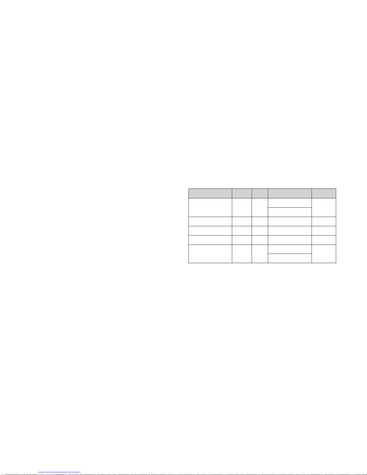
MODE
POWER ON (NORMAL)
STAND-BY
SUSPEND
DPMS OFF
POWER OFF
H/V SYNC
ON/ON
OFF/ON
ON/OFF
OFF/OFF
OFF/OFF
POWER CONSUMPTION
less than 270W-With PC
less than 240W-Only MNT
less than 15W-Only MNT
less than 15W-Only MNT
less than 15W-Only MNT
less than 20W-With PC
less than 13W-Only MNT
LED COLOR
GREEN
AMBER
AMBER
AMBER
OFF
VIDEO
ACTIVE
OFF
OFF
OFF
OFF
- 3 -
WARNING FOR THE SAFETY-RELATED COMPONENT.
• There are some special components used in LCD
monitor that are important for safety. These parts are
marked on the schematic diagram and the
replacement parts list. It is essential that these critical
parts should be replaced with the manufacturer’s
specified parts to prevent electric shock, fire or other
hazard.
• Do not modify original design without obtaining written
permission from manufacturer or you will void the
original parts and labor guarantee.
TAKE CARE DURING HANDLING THE LCD MODULE
WITH BACKLIGHT UNIT.
• Must mount the module using mounting holes arranged
in four corners.
• Do not press on the panel, edge of the frame strongly
or electric shock as this will result in damage to the
screen.
• Do not scratch or press on the panel with any sharp
objects, such as pencil or pen as this may result in
damage to the panel.
• Protect the module from the ESD as it may damage the
electronic circuit (C-MOS).
• Make certain that treatment person’s body are
grounded through wrist band.
• Do not leave the module in high temperature and in
areas of high humidity for a long time.
• The module not be exposed to the direct sunlight.
• Avoid contact with water as it may a short circuit within
the module.
• If the surface of panel become dirty, please wipe it off
with a softmaterial. (Cleaning with a dirty or rough cloth
may damage the panel.)
WARNING
BE CAREFUL ELECTRIC SHOCK !
• If you want to replace with the new backlight (CCFL) or
inverter circuit, must disconnect the AC adapter
because high voltage appears at inverter circuit about
650Vrms.
• Handle with care wires or connectors of the inverter
circuit. If the wires are pressed cause short and may
burn or take fire.
Leakage Current Hot Check Circuit
• Replaceable batteries
① CAUTION
RISK OF EXPLOSION IF BATTERY IS REPLACED BY
AN INCORRECT TYPE.
DISPOSE OF USED BATTERIES ACCORDING TO
THE INSTRUCTIONS
② ADVARSEL
Lithiumbatteri - Eksplosionsfare ved fejlagtig
hándtening.
Udskiftning má kun ske med batteri at samme fabrikat
og type.
Levér det brugte batteri tilbage til leverandoren.
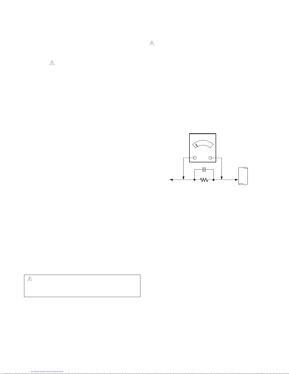
PRECAUTION
CAUTION
Please use only a plastic screwdriver to protect yourself
from shock hazard during service operation.
1.5 Kohm/10W
To Instrument's
exposed
METALLIC PARTS
Good Earth Ground
such as WATER PIPE,
CONDUIT etc.
AC Volt-meter

- 4 -
SERVICING PRECAUTIONS
CAUTION: Before servicing receivers covered by this
service manual and its supplements and addenda, read
and follow the SAFETY PRECAUTIONS on page 3 of this
publication.
NOTE: If unforeseen circumstances create conflict
between the following servicing precautions and any of the
safety precautions on page 3 of this publication, always
follow the safety precautions. Remember: Safety First.
General Servicing Precautions
1. Always unplug the receiver AC power cord from the AC
power source before;
a. Removing or reinstalling any component, circuit
board module or any other receiver assembly.
b. Disconnecting or reconnecting any receiver electrical
plug or other electrical connection.
c. Connecting a test substitute in parallel with an
electrolytic capacitor in the receiver.
CAUTION: A wrong part substitution or incorrect
polarity installation of electrolytic capacitors may
result in an explosion hazard.
d. Discharging the picture tube anode.
2. Test high voltage only by measuring it with an
appropriate high voltage meter or other voltage
measuring device (DVM, FETVOM, etc) equipped with
a suitable high voltage probe.
Do not test high voltage by "drawing an arc".
3. Discharge the picture tube anode only by (a) first
connecting one end of an insulated clip lead to the
degaussing or kine aquadag grounding system shield
at the point where the picture tube socket ground lead
is connected, and then (b) touch the other end of the
insulated clip lead to the picture tube anode button,
using an insulating handle to avoid personal contact
with high voltage.
4. Do not spray chemicals on or near this receiver or any
of its assemblies.
5. Unless specified otherwise in this service manual,
clean electrical contacts only by applying the following
mixture to the contacts with a pipe cleaner, cottontipped stick or comparable non-abrasive applicator;
10% (by volume) Acetone and 90% (by volume)
isopropyl alcohol (90%-99% strength)
CAUTION: This is a flammable mixture.
Unless specified otherwise in this service manual,
lubrication of contacts in not required.
6. Do not defeat any plug/socket B+ voltage interlocks
with which receivers covered by this service manual
might be equipped.
7. Do not apply AC power to this instrument and/or any of
its electrical assemblies unless all solid-state device
heat sinks are correctly installed.
8. Always connect the test receiver ground lead to the
receiver chassis ground before connecting the test
receiver positive lead.
Always remove the test receiver ground lead last.
9. Use with this receiver only the test fixtures specified in
this service manual.
CAUTION: Do not connect the test fixture ground strap
to any heat sink in this receiver.
Electrostatically Sensitive (ES) Devices
Some semiconductor (solid-state) devices can be
damaged easily by static electricity. Such components
commonly are called Electrostatically Sensitive (ES)
Devices. Examples of typical ES devices are integrated
circuits and some field-effect transistors and
semiconductor "chip" components. The following
techniques should be used to help reduce the incidence of
component damage caused by static by static electricity.
1. Immediately before handling any semiconductor
component or semiconductor-equipped assembly, drain
off any electrostatic charge on your body by touching a
known earth ground. Alternatively, obtain and wear a
commercially available discharging wrist strap device,
which should be removed to prevent potential shock
reasons prior to applying power to the unit under test.
2. After removing an electrical assembly equipped with
ES devices, place the assembly on a conductive
surface such as aluminum foil, to prevent electrostatic
charge buildup or exposure of the assembly.
3. Use only a grounded-tip soldering iron to solder or
unsolder ES devices.
4. Use only an anti-static type solder removal device.
Some solder removal devices not classified as "antistatic" can generate electrical charges sufficient to
damage ES devices.
5. Do not use freon-propelled chemicals. These can
generate electrical charges sufficient to damage ES
devices.
6. Do not remove a replacement ES device from its
protective package until immediately before you are
ready to install it. (Most replacement ES devices are
packaged with leads electrically shorted together by
conductive foam, aluminum foil or comparable
conductive material).
7. Immediately before removing the protective material
from the leads of a replacement ES device, touch the
protective material to the chassis or circuit assembly
into which the device will be installed.
CAUTION: Be sure no power is applied to the chassis
or circuit, and observe all other safety precautions.
8. Minimize bodily motions when handling unpackaged
replacement ES devices. (Otherwise harmless motion
such as the brushing together of your clothes fabric or
the lifting of your foot from a carpeted floor can
generate static electricity sufficient to damage an ES
device.)

- 5 -
General Soldering Guidelines
1. Use a grounded-tip, low-wattage soldering iron and
appropriate tip size and shape that will maintain tip
temperature within the range or 500。F to 600。F.
2. Use an appropriate gauge of RMA resin-core solder
composed of 60 parts tin/40 parts lead.
3. Keep the soldering iron tip clean and well tinned.
4. Thoroughly clean the surfaces to be soldered. Use a
mall wire-bristle (0.5 inch, or 1.25cm) brush with a
metal handle.
Do not use freon-propelled spray-on cleaners.
5. Use the following unsoldering technique
a. Allow the soldering iron tip to reach normal
temperature.
(500。F to 600。F)
b. Heat the component lead until the solder melts.
c. Quickly draw the melted solder with an anti-static,
suction-type solder removal device or with solder
braid.
CAUTION: Work quickly to avoid overheating the
circuitboard printed foil.
6. Use the following soldering technique.
a. Allow the soldering iron tip to reach a normal
temperature (500。F to 600。F)
b. First, hold the soldering iron tip and solder the strand
against the component lead until the solder melts.
c. Quickly move the soldering iron tip to the junction of
the component lead and the printed circuit foil, and
hold it there only until the solder flows onto and
around both the component lead and the foil.
CAUTION: Work quickly to avoid overheating the
circuit board printed foil.
d. Closely inspect the solder area and remove any
excess or splashed solder with a small wire-bristle
brush.
IC Remove/Replacement
Some chassis circuit boards have slotted holes (oblong)
through which the IC leads are inserted and then bent flat
against the circuit foil. When holes are the slotted type,
the following technique should be used to remove and
replace the IC. When working with boards using the
familiar round hole, use the standard technique as
outlined in paragraphs 5 and 6 above.
Removal
1. Desolder and straighten each IC lead in one operation
by gently prying up on the lead with the soldering iron
tip as the solder melts.
2. Draw away the melted solder with an anti-static
suction-type solder removal device (or with solder
braid) before removing the IC.
Replacement
1. Carefully insert the replacement IC in the circuit board.
2. Carefully bend each IC lead against the circuit foil pad
and solder it.
3. Clean the soldered areas with a small wire-bristle
brush. (It is not necessary to reapply acrylic coating to
the areas).
"Small-Signal" Discrete Transistor
Removal/Replacement
1. Remove the defective transistor by clipping its leads as
close as possible to the component body.
2. Bend into a "U" shape the end of each of three leads
remaining on the circuit board.
3. Bend into a "U" shape the replacement transistor leads.
4. Connect the replacement transistor leads to the
corresponding leads extending from the circuit board
and crimp the "U" with long nose pliers to insure metal
to metal contact then solder each connection.
Power Output, Transistor Device
Removal/Replacement
1. Heat and remove all solder from around the transistor
leads.
2. Remove the heat sink mounting screw (if so equipped).
3. Carefully remove the transistor from the heat sink of the
circuit board.
4. Insert new transistor in the circuit board.
5. Solder each transistor lead, and clip off excess lead.
6. Replace heat sink.
Diode Removal/Replacement
1. Remove defective diode by clipping its leads as close
as possible to diode body.
2. Bend the two remaining leads perpendicular y to the
circuit board.
3. Observing diode polarity, wrap each lead of the new
diode around the corresponding lead on the circuit
board.
4. Securely crimp each connection and solder it.
5. Inspect (on the circuit board copper side) the solder
joints of the two "original" leads. If they are not shiny,
reheat them and if necessary, apply additional solder.
Fuse and Conventional Resistor
Removal/Replacement
1. Clip each fuse or resistor lead at top of the circuit board
hollow stake.
2. Securely crimp the leads of replacement component
around notch at stake top.
3. Solder the connections.
CAUTION: Maintain original spacing between the
replaced component and adjacent components and the
circuit board to prevent excessive component
temperatures.

- 6 -
Circuit Board Foil Repair
Excessive heat applied to the copper foil of any printed
circuit board will weaken the adhesive that bonds the foil
to the circuit board causing the foil to separate from or
"lift-off" the board. The following guidelines and
procedures should be followed whenever this condition is
encountered.
At IC Connections
To repair a defective copper pattern at IC connections use
the following procedure to install a jumper wire on the
copper pattern side of the circuit board. (Use this
technique only on IC connections).
1. Carefully remove the damaged copper pattern with a
sharp knife. (Remove only as much copper as
absolutely necessary).
2. carefully scratch away the solder resist and acrylic
coating (if used) from the end of the remaining copper
pattern.
3. Bend a small "U" in one end of a small gauge jumper
wire and carefully crimp it around the IC pin. Solder the
IC connection.
4. Route the jumper wire along the path of the out-away
copper pattern and let it overlap the previously scraped
end of the good copper pattern. Solder the overlapped
area and clip off any excess jumper wire.
At Other Connections
Use the following technique to repair the defective copper
pattern at connections other than IC Pins. This technique
involves the installation of a jumper wire on the
component side of the circuit board.
1. Remove the defective copper pattern with a sharp
knife.
Remove at least 1/4 inch of copper, to ensure that a
hazardous condition will not exist if the jumper wire
opens.
2. Trace along the copper pattern from both sides of the
pattern break and locate the nearest component that is
directly connected to the affected copper pattern.
3. Connect insulated 20-gauge jumper wire from the lead
of the nearest component on one side of the pattern
break to the lead of the nearest component on the
other side.
Carefully crimp and solder the connections.
CAUTION: Be sure the insulated jumper wire is
dressed so the it does not touch components or sharp
edges.

TIMING CHART
- 7 -
VIDEO
SYNC
B
C
E
A
D
<< Dot Clock (MHz), Horizontal Frequency (kHz), Vertical Frequency (Hz), Horizontal etc... (µs), Vertical etc... (ms) >>
1 H(Pixels) + 25.175 31.469 800 640 16 96 48 640 x 350
V(Lines) - 70.8 449 350 37 2 60
2 H(Pixels) - 28.321 31.468 900 720 18 108 54 720 X 400
V(Lines) + 70.8 449 400 12 2 35
3 H(Pixels) - 25.175 31.469 800 640 16 96 48 640 x 480
V(Lines) - 59.94 525 480 10 2 33
4 H(Pixels) - 31.5 37.5 840 640 16 64 120 640 x 480
V(Lines) - 75 500 480 1 3 16
5 H(Pixels) - 36.0 43.269 832 640 56 56 80 640 x 480
V(Lines) - 85.0 509 480 1 3 25
6 H(Pixels) + 40.0 37.879 1056 800 40 128 88 800 x 600
V(Lines) + 60.317 628 600 1 4 23
7 H(Pixels) + 49.5 46.875 1056 800 16 80 160 800 x 600
V(Lines) + 75.0 625 600 1 3 21
8 H(Pixels) + 56.25 53.674 1048 800 32 64 152 800 x 600
V(Lines) + 85.061 631 600 1 3 27
9 H(Pixels) +/- 57.283 49.725 1152 832 32 64 224 832 x 624
V(Lines) +/- 74.55 667 624 1 3 39
10 H(Pixels) - 65.0 48.363 1344 1024 24 136 160 1024 x 768
V(Lines) - 60.0 806 768 3 6 29
11 H(Pixels) - 78.75 60.123 1312 1024 16 96 176 1024 x 768
V(Lines) - 75.029 800 768 1 3 28
12 H(Pixels) + 94.5 68.68 1376 1024 48 96 208 1024 x 768
V(Lines) + 85.00 808 768 1 3 36
13 H(Pixels) + 74.5 44.772 1664 1280 64 128 192 1280 x 720
V(Lines) + 59.855 748 720 3 5 20
14 H(Pixels) + 84.75 47.72 1776 1360 72 136 208 1360 x 768
V(Lines) + 59.799 798 768 3 5 22
15 H(Pixels) + 108.0 63.981 1688 1280 48 112 248 1280 x 1024
V(Lines) + 60.02 1066 1024 1 3 38
16 H(Pixels) + 135.00 79.98 1688 1280 16 144 248 1280 x 1024
V(Lines) + 75.02 1066 1024 1 3 38
17 H(Pixels) + 162.00 75.00 2160 1600 90 30 88 1600 x 1200
V(Lines) + 60 1250 1200 1 3 46
※1~17 : D-SUB, 1~15 : DVI-D
MODE
H / V
Sync
Polarity
Dot
Clock
Frequency
Total
Period
( E )
Video
Active
Time ( A )
Front
Porch
( C )
Sync
Duration
( D )
Back
Porch
( F )
Resolution
- 8 -
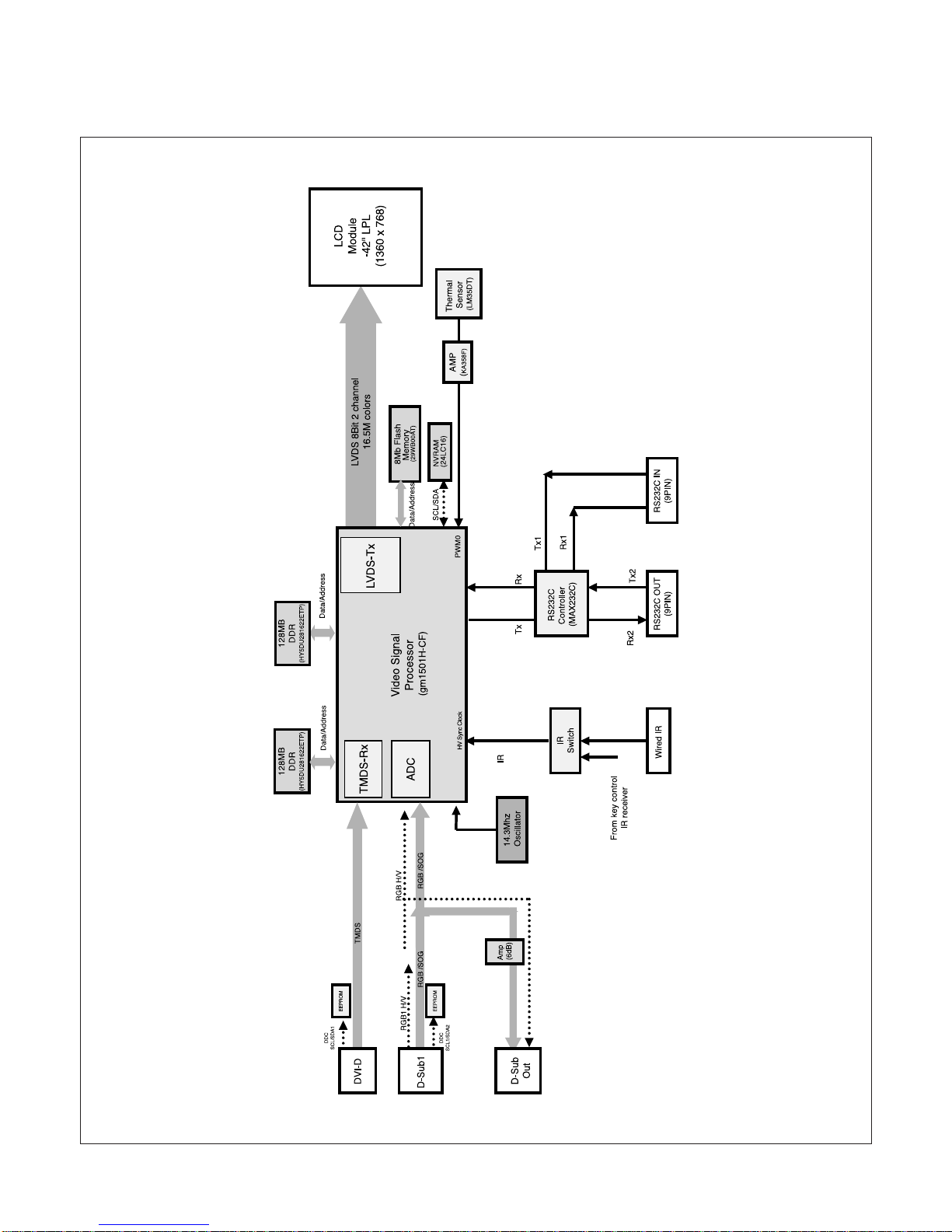
BLOCK DIAGRAM(gm1501H)-MAIN BOARD

DESCRIPTION OF BLOCK DIAGRAM(gm1501)-MAIN BOARD
- 9 -
1. VIDEO SIGNAL PROCESSOR (FORMAT CONVERTER)
This section is composed of gm1501H(U402) and peripheral devices.
gm1501H(SCALER_U402) have in built u-COM in IC.
(1) This IC include A/D Converter, Pre-Amp, PLL Circuit.
(2) This IC include TMDS Receiver and LVDS Transmitter. TMDS Receiver is decoding input DVI Signal and LVDS
Transmitter is encoding the output Signal. Also, gm1501H have Format Converter (Scaling) function.
This IC convert Various sized Digital signal to LCD Module's resolution (WXGA).
2. DC/DC COVERTER
DC/DC Converters change Power output voltage (DC 5V, 12V, 24V) to 1.5V, 2.5V, 3.3V, 5V, 8V, 9V.
(To be used by different IC on the main board.)
3. TEMPERATURE SENSING AND FAN CONTROL
This section is composed of LM35DT(U523), KIA358F(U524) and peripheral devices.
The temperature at surface of LM35DT(U523) is sensed and converted to HEX code by KIA358(U524).
gm1501H(U402) receives sensing HEX values from KIA358F(U524)and control FAN(42INCH ONLY).
4. POWER SUPPLY BLOCK
Power supply receives AC voltage (100-240V, 50/60Hz,) and converts to System voltage that are 5V, 12V, 18V and 24V DC
voltage.
These voltages supports main board, inverter board and module's T-con board.
This Circuit contains PFC (Power Factor Correction) circuit.
The Minimum Power efficiency is about 75%.
5. DDC COTROLLER
This section is composed gm1501H(U402),EEPROM IC (U404, U114, U120) and peripheral devices.
gm1501H(U402) is controlling peripheral devices through IIC Line.
Major functions of this block are :
(1) Controlling of u-COM and Flash memory through DDC-SCLA, DDC-SDAA of D-sub connector.
(2) Storage of EDID DATA in the EEPROM(U114, U120).
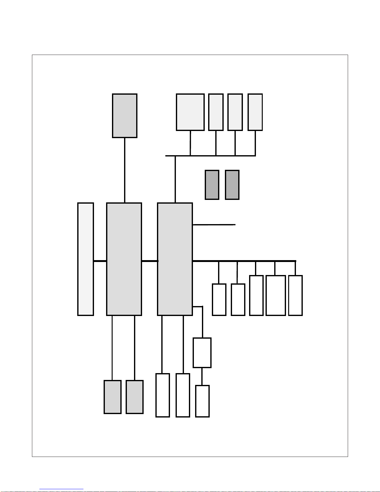
BLOCK DIAGRAM(LV-671)-MOTHER BOARD
- 10 -
Chip Set
Chip Set
82855GME
400MHz FSB
ATAPI Devices
Intel Pentium M Processor 1.7GHz
82801GME
Mini-AGP
1x184-Pin
DIMM
512MB
Slim PCI
Mini-PCI
PCMCIA
Audio
AC97
Coder
COM Port
Parallel
Port
PS/2
Floppy
IrDA
DDR266/333MHz
LCD
LVDS
AGP 4x DVO B/C
Ultra A T A100
ATAPI Devices
USB 2.0 480Mb/s
LPC
PCI Bus
33MHz
Compact Flash
Gigabit
Ethernet
Controller
25Mhz
Oscillator
24.576Mhz
Oscillator

DESCRIPTION OF BLOCK DIAGRAM(LV-671)-MOTHER BOARD
- 11 -
1. Form Factor Mini-ITX compact mother board
2. CPU Onboard Intel Celeron M 600MHz
Package : mBGA479
L2 Cache : none
Front side bus : 400MHz
Optional Enhanced Intel SpeedStep£ technology support
3. Memory 1 x 184-pin DDR200/266 SDRAM up to 1GB
4 Chipset Intel 852GM and ICH4
5. Real Time Clock Chipset integrated RTC with onboard lithium battery
6. Watchdog Timer Generates a system reset with internal timer for 1min ~ 255min
7. Power Management ACPI 1.0 compliant, supports power saving mode with ATX PSU
8. PCI Enhanced IDE Two UltraATA/100 IDE channels up to 4 ATAPI devices
9. VGA Interface Intel 852GM builds in Intel Extreme Graphic 2 technology
10. Video Memory Up to 64MB shared with system memory
11. Audio Interface Intel ICH4 integrated with Realtek ALC655 5.1 CHAC97 Codec
12. LAN Interface 1 x tel 82540EM Gigabit Ethernet Controller
13. LCD Interface 24-bit dual-channel LVDS interface up to 1400 x 1050 of resolution
14. Solid State Disk IDE1 supports Disk On Module with +5V power supply
1 x Compact Flash Type II socket
15. GPIO Interface Onboard programmable 16-bit Digital I/O interface
16. Extended Interface 1 x Mini-PCI or 1 x Mini-AGP (DVO supported only) socket
1 x PCMCIA type II card bus slot
1 x slim type PCI slot
17. Internal I/O Port 1 x audio header for MIC-in / Line -in / Line-out, 1 x CD audio-in, 1 x DC12V / 5V output, 1 x slim type
floppy pore
18. External I/O Port 1 x RJ45 LAN ports, 1 x DB15 VGA port and 1 x PS / 2 Keyboard / Mouse Port, 2 x RS232 Serial Ports, 1
x amplified Speaker out, 1 x S/PDIF, 2 x USB2.0 ports, 1 x parallel port, 1 x DC-in mini-DIN

- 12 -
 Loading...