

Page 1

- 1-1 -
[CONTENTS]
❍ SECTION 1.GENERAL
• SERVICING PRECAUTIONS . . . . . . . . . . . . . . . . . . . . . . . . . . . . . . . . . . . . . . . . . . . . . . . 1-2
• ESD PRECAUTIONS . . . . . . . . . . . . . . . . . . . . . . . . . . . . . . . . . . . . . . . . . . . . . . . . . . . . . 1-4
❍ SECTION 2.ELECTRICAL SECTION
• TROUBLESHOOTING GUIDE . . . . . . . . . . . . . . . . . . . . . . . . . . . . . . . . . . . . . . . . . . . . . . 2-1
• BLOCK DIAGRAM . . . . . . . . . . . . . . . . . . . . . . . . . . . . . . . . . . . . . . . . . . . . . . . . . . . . . . . 2-11
• SCHEMATIC DIAGRAMS . . . . . . . . . . . . . . . . . . . . . . . . . . . . . . . . . . . . . . . . . . . . . . . . . 2-13
• WIRING DIAGRAM . . . . . . . . . . . . . . . . . . . . . . . . . . . . . . . . . . . . . . . . . . . . . . . . . . . . . . 2-27
• PRINTED CIRCUIT BOARD DIAGRAM . . . . . . . . . . . . . . . . . . . . . . . . . . . . . . . . . . . . . . . 2-29
❍ SECTION 3.DVD PART
• DVD ELECTRICAL TROUBLESHOOTING GUIDE . . . . . . . . . . . . . . . . . . . . . . . . . . . . . . . 3-1
• INTERNAL BLOCK DIAGRAM of ICs . . . . . . . . . . . . . . . . . . . . . . . . . . . . . . . . . . . . . . . . . . 3-7
• SCHEMATIC DIAGRAM . . . . . . . . . . . . . . . . . . . . . . . . . . . . . . . . . . . . . . . . . . . . . . . . . . . 3-27
• PRINTED CIRCUIT BOARD DIAGRAM . . . . . . . . . . . . . . . . . . . . . . . . . . . . . . . . . . . . . . . 3-33
❍ SECTION 4. EXPLODED VIEWS
• CABINET AND MAIN FRAME SECTION . . . . . . . . . . . . . . . . . . . . . . . . . . . . . . . . . . . . . . . 4-1
• TAPE DECK MECHANISM (A/R & A/S : LEFT A/S DECK) . . . . . . . . . . . . . . . . . . . . . . . . . . 4-5
• TAPE DECK MECHANISM (A/R & A/S : RIGHT A/R DECK) . . . . . . . . . . . . . . . . . . . . . . . . .4-7
❍ SECTION 5. SPEAKER PART . . . . . . . . . . . . . . . . . . . . . . . . . . . . . . . . . . . . .5-1
❍ SECTION 6. REPLACEMENT PARTS LIST . . . . . . . . . . . . . . . . . . . . . . . . . . .6-1
Page 2
- 1-2 -
SECTION 1. GENERAL
❏ SERVICING PRECAUTIONS
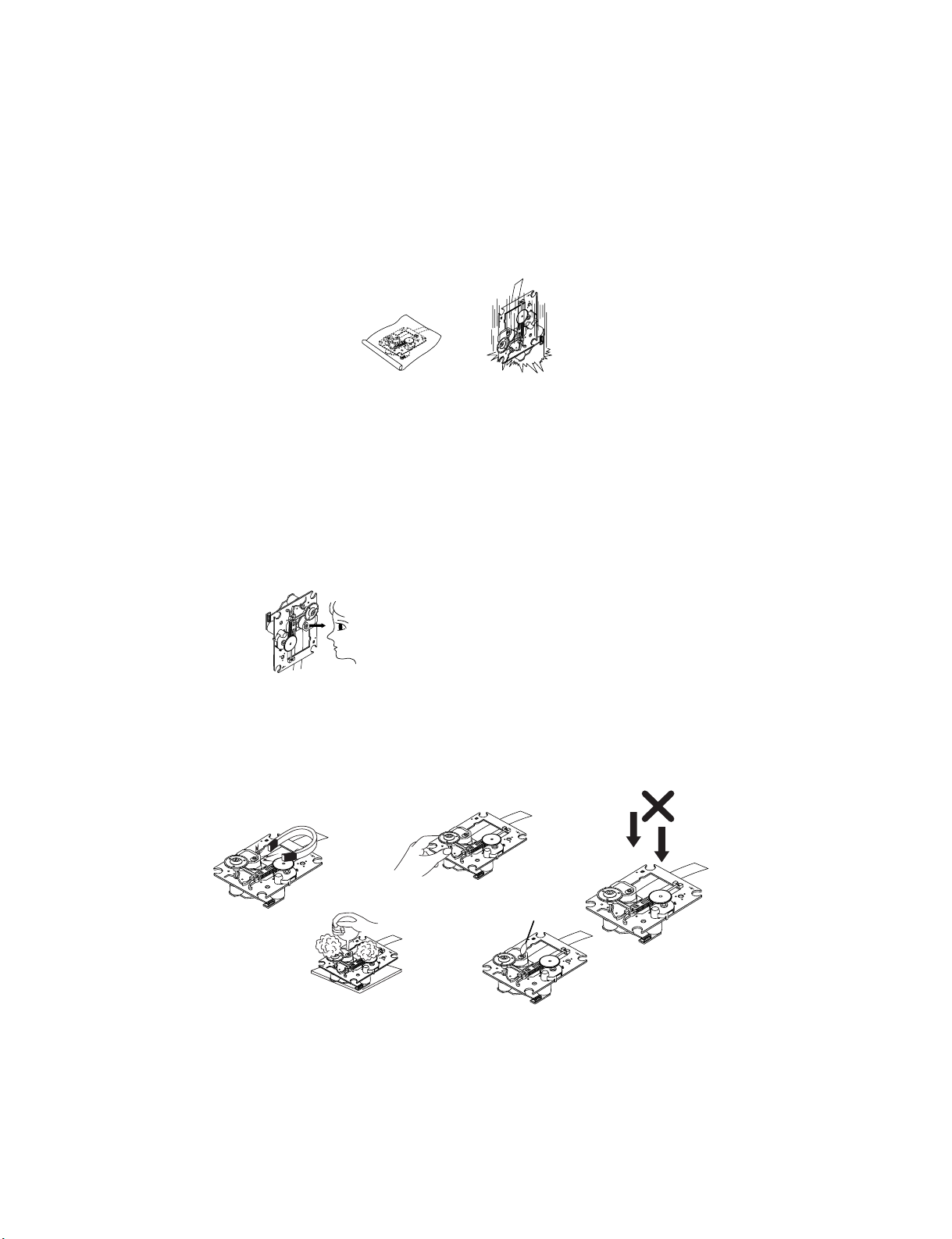
NOTES REGARDING HANDLING OF THE PICK-UP
1. Notes for transport and storage
1) The pick-up should always be left in its conductive bag until immediately prior to use.
2) The pick-up should never be subjected to external pressure or impact.
2. Repair notes
1) The pick-up incorporates a strong magnet, and so should never be brought close to magnetic materials.
2) The pick-up should always be handled correctly and carefully, taking care to avoid external pressure and
impact. If it is subjected to strong pressure or impact, the result may be an operational malfunction and/or
damage to the printed-circuit board.
3) Each and every pick-up is already individually adjusted to a high degree of precision, and for that reason
the adjustment point and installation screws should absolutely never be touched.
4) Laser beams may damage the eyes!
Absolutely never permit laser beams to enter the eyes!
Also NEVER switch ON the power to the laser output part (lens, etc.) of the pick-up if it is damaged.
5) Cleaning the lens surface
If there is dust on the lens surface, the dust should be cleaned away by using an air bush (such as used
for camera lens). The lens is held by a delicate spring. When cleaning the lens surface, therefore, a cotton
swab should be used, taking care not to distort this.
6) Never attempt to disassemble the pick-up.
Spring by excess pressure. If the lens is extremely dirty, apply isopropyl alcohol to the cotton swab. (Do
not use any other liquid cleaners, because they will damage the lens.) Take care not to use too much of
this alcohol on the swab, and do not allow the alcohol to get inside the pick-up.
Storage in conductive bag
Drop impact
NEVER look directly at the laser beam, and don’t let
contact fingers or other exposed skin.
Magnet
How to hold the pick-up
Conductive Sheet
Cotton swab
Pressure
Pressure
Page 3
- 1-3 -
NOTES REGARDING COMPACT DISC PLAYER REPAIRS
1. Preparations
1) Compact disc players incorporate a great many ICs as well as the pick-up (laser diode). These components
are sensitive to, and easily affected by, static electricity. If such static electricity is high voltage, components
can be damaged, and for that reason components should be handled with care.
2) The pick-up is composed of many optical components and other high-precision components. Care must be
taken, therefore, to avoid repair or storage where the temperature of humidity is high, where strong magnetism is present, or where there is excessive dust.
2. Notes for repair
1) Before replacing a component part, first disconnect the power supply lead wire from the unit
2) All equipment, measuring instruments and tools must be grounded.
3) The workbench should be covered with a conductive sheet and grounded.
When removing the laser pick-up from its conductive bag, do not place the pick-up on the bag. (This is
because there is the possibility of damage by static electricity.)
4) To prevent AC leakage, the metal part of the soldering iron should be grounded.
5) Workers should be grounded by an armband (1M Ω)
6) Care should be taken not to permit the laser pick-up to come in contact with clothing, in order to prevent static electricity changes in the clothing to escape from the armband.
7) The laser beam from the pick-up should NEVER be directly facing the eyes or bare skin.
CLEARING MALFUNCTION
You can reset your unit to initial status if malfunction occur(button malfunction, display, etc.).
Using a pointed good conductor(such as driver), simply short the RESET jump wire on the inside of
the volume knob for more than 3 seconds.
If you reset your unit, you must reenter all its settings(stations, clock, timer)
NOTE: 1.To operate the RESET jump wire, pull the volume rotary knob and release it.
2. If you wish to operate the RESET jump wire, it is necessary to unplug the power cord.
Resistor
(1 Mohm)
Conductive
Sheet
Resistor
(1 Mohm)
Armband
RESET jump wire
VOLUME
VOLUME KNOB
DOWN
UP
Page 4
- 1-4 -
❏ ESD PRECAUTIONS
Electrostatically Sensitive Devices (ESD)
Some semiconductor (solid state) devices can be damaged easily by static electricity. Such components
commonly are called Electrostatically Sensitive Devices (ESD). Examples of typical ESD devices are integrated
circuits and some field-effect transistors and semiconductor chip components.The following techniques should
be used to help reduce the incidence of component damage caused by static electricity.
1. Immediately before handling any semiconductor component or semiconductor-equipped assembly, drain off
any electrostatic charge on your body by touching a known earth ground. Alternatively, obtain and wear a
commercially available discharging wrist strap device, which should be removed for potential shock reasons
prior to applying power to the unit under test.
2. After removing an electrical assembly equipped with ESD devices, place the assembly on a conductive sur-
face such as aluminum foil, to prevent electrostatic charge buildup or exposure of the assembly.
3. Use only a grounded-tip soldering iron to solder or unsolder ESD devices.
4. Use only an anti-static solder removal device. Some solder removal devices not classified as "anti-static" can
generate electrical charges sufficient to damage ESD devices.
5. Do not use freon-propelled chemicals. These can generate electrical charges sufficient to damage ESD
devices.
6. Do not remove a replacement ESD device from its protective package until immediately before you are
ready to install it. (Most replacement ESD devices are packaged with leads electrically shorted together by
conductive foam, aluminum foil or comparable conductive materials).
7. Immediately before removing the protective material from the leads of a replacement ESD device, touch the
protective material to the chassis or circuit assembly into which the device will by installed.
CAUTION : BE SURE NO POWER IS APPLIED TO THE CHASSIS OR CIRCUIT, AND OBSERVE ALL
OTHER SAFETY PRECAUTIONS.
8. Minimize bodily motions when handing unpackaged replacement ESD devices. (Otherwise harmless motion
such as the brushing together of your clothes fabric or the lifting of your foot from a carpeted floor can generate static electricity sufficient to damage an ESD device).
CAUTION. GRAPHIC SYMBOLS
THE LIGHTNING FLASH WITH APROWHEAD SYMBOL. WITHIN AN EQUILATERAL TRIANGLE, IS
INTENDED TO ALERT THE SERVICE PERSONNEL TO THE PRESENCE OF UNINSULATED “DANGEROUS VOLTAGE” THAT MAY BE OF SUFFICIENT MAGNITUDE TO CONSTITUTE A RISK OF
ELECTRIC SHOCK.
THE EXCLAMATION POINT WITHIN AN EQUILATERAL TRIANGLE IS INTENDED TO ALERT THE
SERVICE PERSONNEL TO THE PRESENCE OF IMPORTANT SAFETY INFORMATION IN SERVICE
LITERATURE.
Page 5

- 1-6 -
Page 6
- 2-1 -
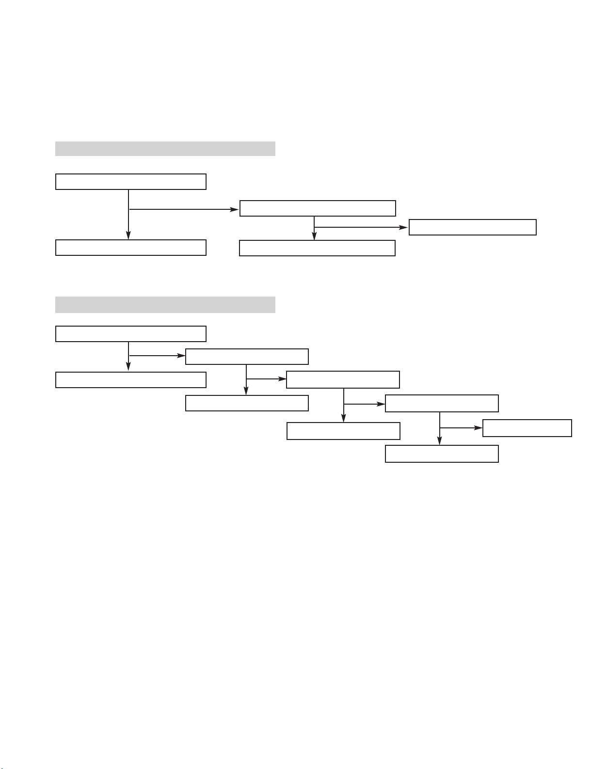
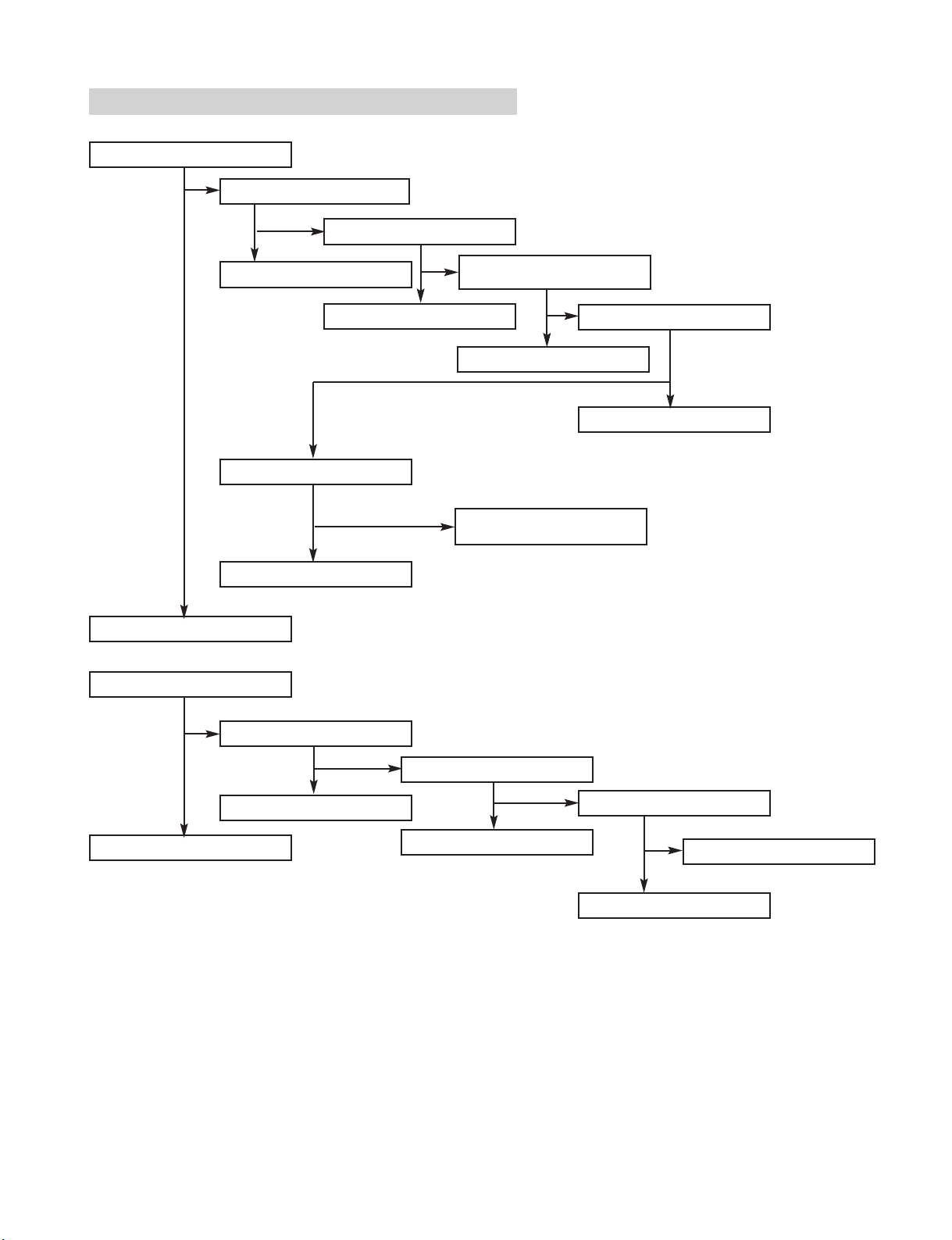
SECTION 2. ELECTRICAL
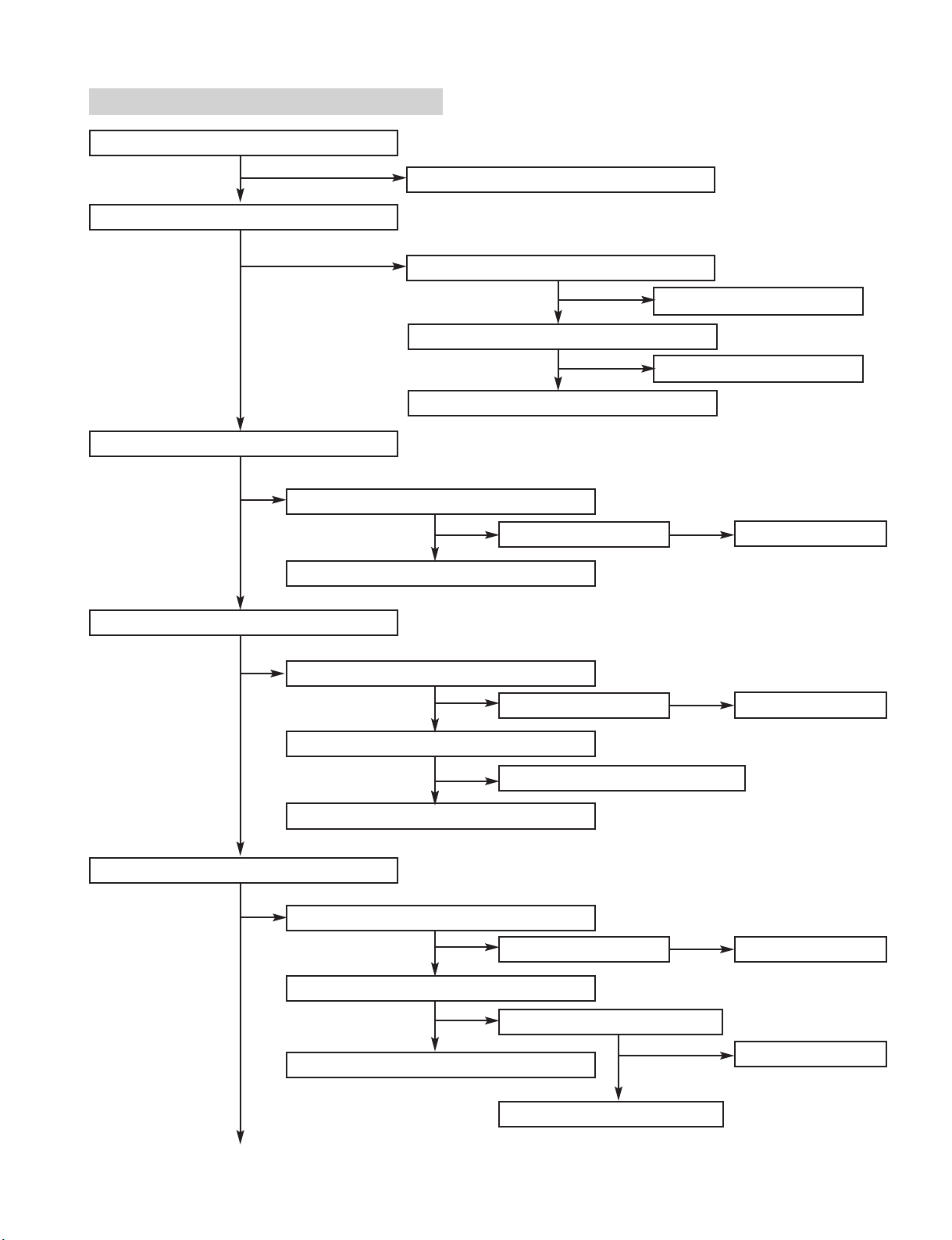
VKK CHECK
P-SENS CHECK
PN903 PIN5, CN302 PIN5 DC -33V check
IC301 PIN51 DC -33V check
ZD900 voltage check (+5.1V)
IC301 PIN26 check
ZD901(+) -33V check
D901(+) waveform check
D901 replacement
R902 check ZD900 replacement
Q902 TURN ON check
C919(-) -33V
up to
check
D908, D909 replacement
Troubleshooting check
Q902 replacement
normal
❏ TROUBLESHOOTING GUIDE
YES
YES
NO
NO
NO
YES
YES
YES
YES
NO
NO
NO
Page 7
- 2-2 -
POWER CHECK
Every kinds of Fuse check
IC700 “12”(+VH2), 6(-VH2) PIN DC power output check
Fuse replacement
PN900 PIN1, 5 DC voltage output check
D900 PIN2, 3 AC check replacement
OK
D900 replacement
Transformer replacement
CN901 PIN5 +12V(D) power check
CN901 PIN6, 7 DC +16V over power check
D901 AC voltage input check
Transformer replacement
IC902(7812) assemble check replacement
YES
YES
YES
YES
YES
YES
NO
NO
NO
NO
NO
NO NO
CN901 PIN3 +6.2V(D) power check
D913 AC voltage input check
IC902(7812) assemble check replacement
Transformer replacement
CN901 PIN6, 7 DC +16V up to power check
CN901 PIN5 +12V(D) power check
IC901(7805) assemble check replacement
YES
YES
YES
NO
NO
NO
NO
CN901 PIN4 +12V(A) power check
CN901 PIN6, 7 DC +16V over power check
D901 AC voltage input check
IC301
PIN
76 PWR-CTRL “HIGH” check
PATTERN check
Transformer replacement
IC301 replacement
CN901 PIN8 PWR - CTRL “HIGH” check
IC903(78R12) assemble check replacement
YES
YES
YES
YES
NO
NO
NO
NO
NO
Page 8
- 2-3 -
CN901 PIN11 +8V(A) power check
Transformer replacement
CD/DVD/KARAOKE FUNCTION CN901 PIN9
PIN DVDCTRL “HIGH” check
PATTERN Check
IC301 PIN81 DVD-CTRL “HIGH”check
IC301 “81” +16 PIN DC +16 over power check
IC301
replacement
YES
YES
NO
NO
CN901 PIN5 +12V(D) power check
IC904(78R08) check
replacement
D913 AC voltage input check
IC902(7812)
assemble
check
replacement
Transformer replacement
CN901 PIN12 +5V power check
IC901 PIN10 DC +8V over power check
IC905(78R05) power check
D902/D903 AC power input check
YES
YES
YES
YES
NO NO
NO
NO
NO
CN901 PIN14 +3.3V power check
OK
CN901 PIN10 DC +8V over power check
IC907(7805)/IC906(78R33) power check
D902/D903 AC power input check
Transformer replacement
YES
YES
NO
Page 9
- 2-4 -
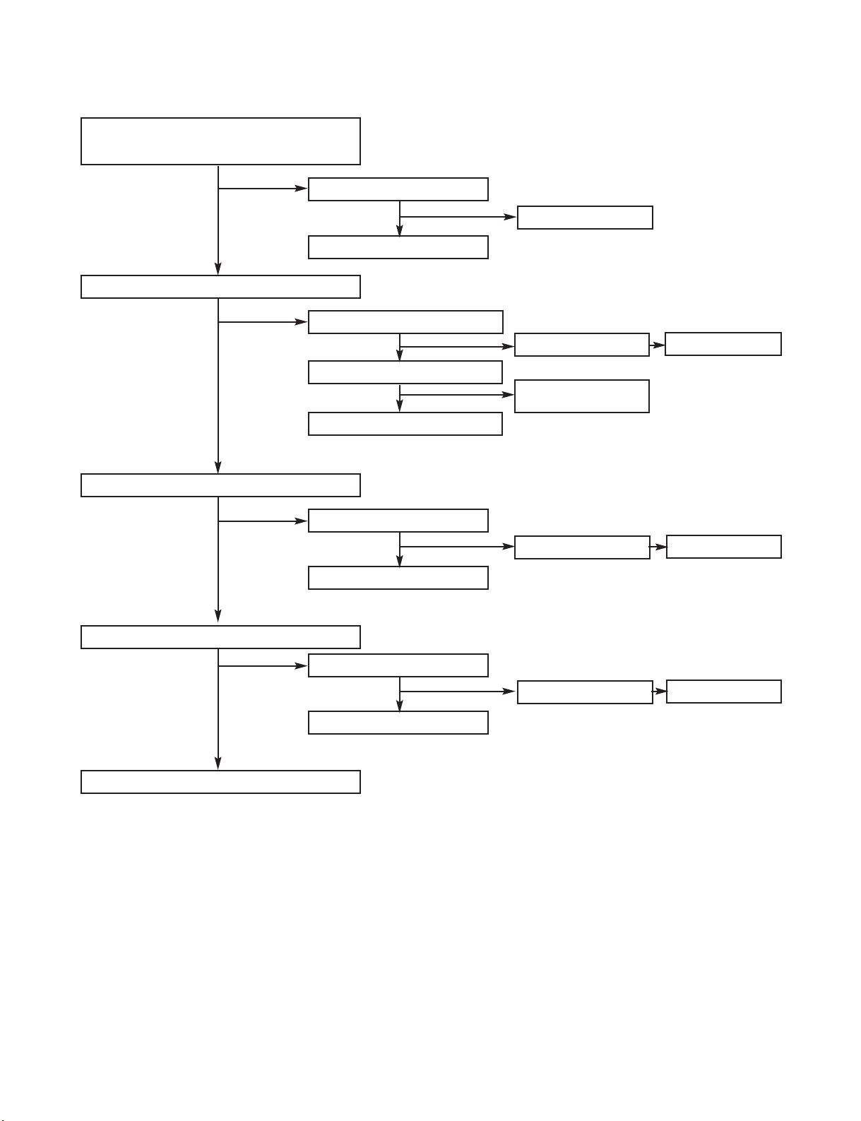
Muting circuit Troubleshooting (if MUTE)
IC301 PIN91 F-MUTE “HIGH” check
Q791 “C” PORT “HIGH” check
Q700/Q750 “C” PORT SIGNAL check
IC301 PIN2 WOOFER-MUTE “HIGH” check
Q741 “C” PORT “HIGH” check
Q740 “C” PORT signal check
Q740 replacement
Q700/Q750 replacement
Muting mode check IC301 replacement
Q791 “E” PORT “HIGH” check
Q791 replacement
normal
normal
Muting mode check IC301 replacement
Q741 “E” PORT HIGH check
Q741 replacement
PATTERN check
PATTERN check
YES
YES
YES
YES
YES
YES
YES
NO
NO
NO
NO
NO
NO
Page 10
- 2-5 -
Q700/750 “C” signal check
JK700 SPEAKER output check
OK
IC602 input check
Q795 “E” HIGH check
RY700 +12V(A) power check
RY700 replacement
IC601 input check
IC602 replacement
IC601 replacement
IC605 replacement
Q1725 TURN-ON check
Speaker short check
OK
Q1720 “B” (+), (-) DC voltage check
IC700 replacement
+12V(A) power Troubleshooting refer
IC605 input check
each function TROUBLESHOOTING refer
no sound
YES
YES
YES
YES
YES
YES
YES
YES
YES
NO
NO
NO
NO
NO
NO
NO
NO
Page 11
- 2-6 -
AUX FUNCTION SPEAKER output
TAPE FUNCTION SPEAKER output
IC700 output check(Front -L/R)
Output sound Troubleshooting refer
IC601 PIN5, 24 input check(AUX -L/R)
IC601 replacement
IC602 PIN2, 9 input check (FRONT -L/R)
IC602 replacement
OK
OK
IC700 input check (Front -L/R)
IC602 PIN2, 19 input check
(FRONT -L/R)
IC700 replacement
IC602 replacement
JK600 AUX input signal cable or
external component sound output check
IC601 PIN4, 25 input check (IN -L/R)
IC605 PIN4, 11 input check
IC202 PIN5, 20 output check(TAPE -L/R)
IC605 replacement
IC601 replacement
IC601 PIN5, 24 input check(IN-L/R)
IC601 replacement
Specific FUNCTION MODE has no sound
YES
YES
YES
YES
YES
YES
YES
YES
YES
YES
NO
NO
NO
NO
NO
NO
NO
NO
Page 12
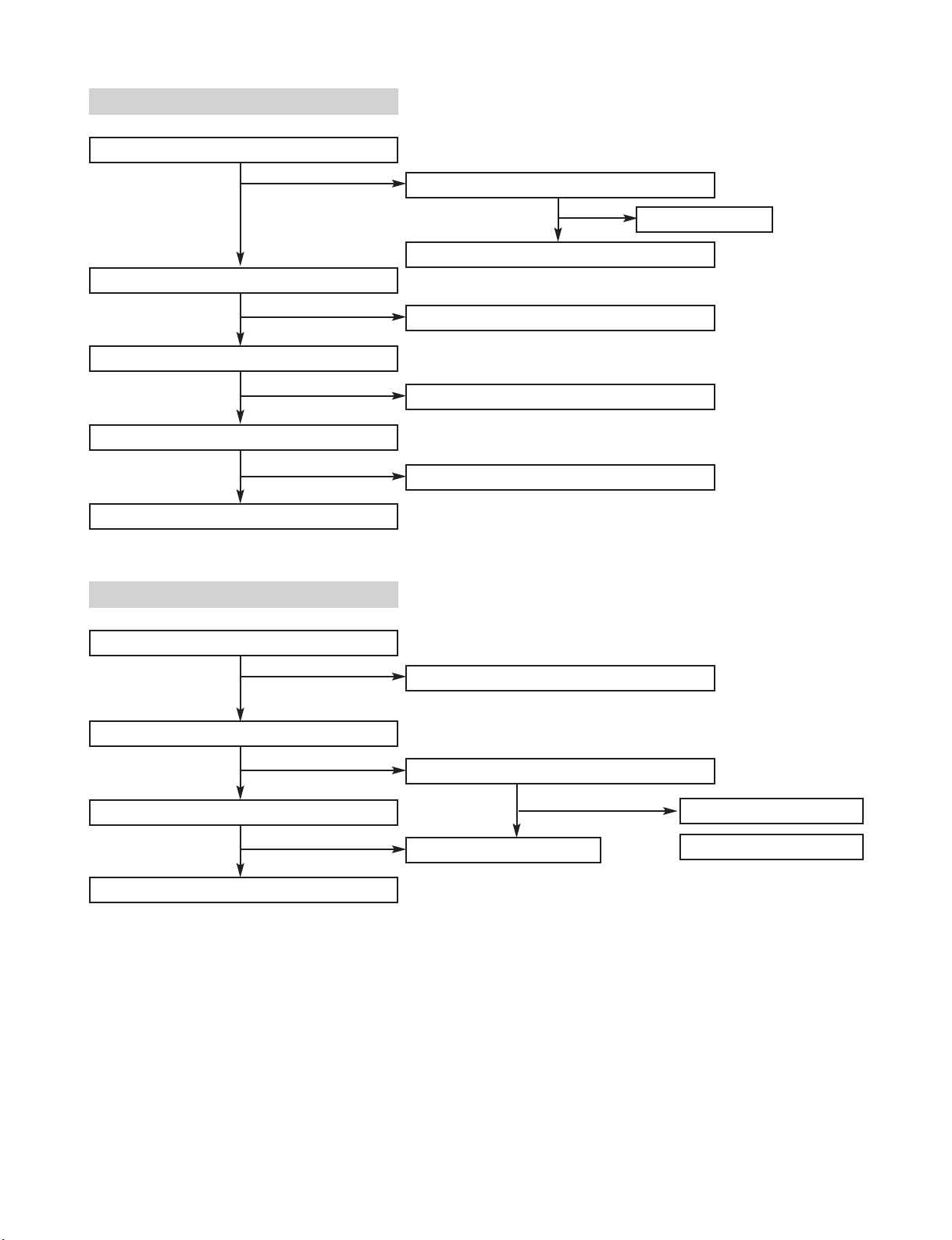
- 2-7 -
CD/DVD function speaker output
OK
IC602 PIN2, 19: F-L/R, 3, 17
PIN : R-L/R, PIN18: CNT input check
IC602 replacement
IC601 replacement
IC601 PIN3, 26 input check
(DVD -L/R)
PN600 PIN2, 4, 8, 10, 12
output check (DVD F-L/R, R-L/R, CNT)
PATTERN check
DVD Troubleshooting refer
TUNER FUNCTION SPEAKER output
OK
IC602 PIN2, 19 input check
(FRONT -L/R)
IC602 replacement
IC601 replacement
TUN100 PIN2 VCC +9V check
TUN100 PLL -CE/CLK/DI/DO ter-
minal DATA correspondence check
IC601 PIN4, 25 input check
(FRONT -L/R)
IC605 PIN3, 5 input check
(TUNER -L/R)
Pattern check
Power +12V(A) check
YES
YES
YES
YES
YES
YES
YES
YES
YES
NO
NO
NO
NO
NO
NO
NO
NO
NO
Page 13
- 2-8 -
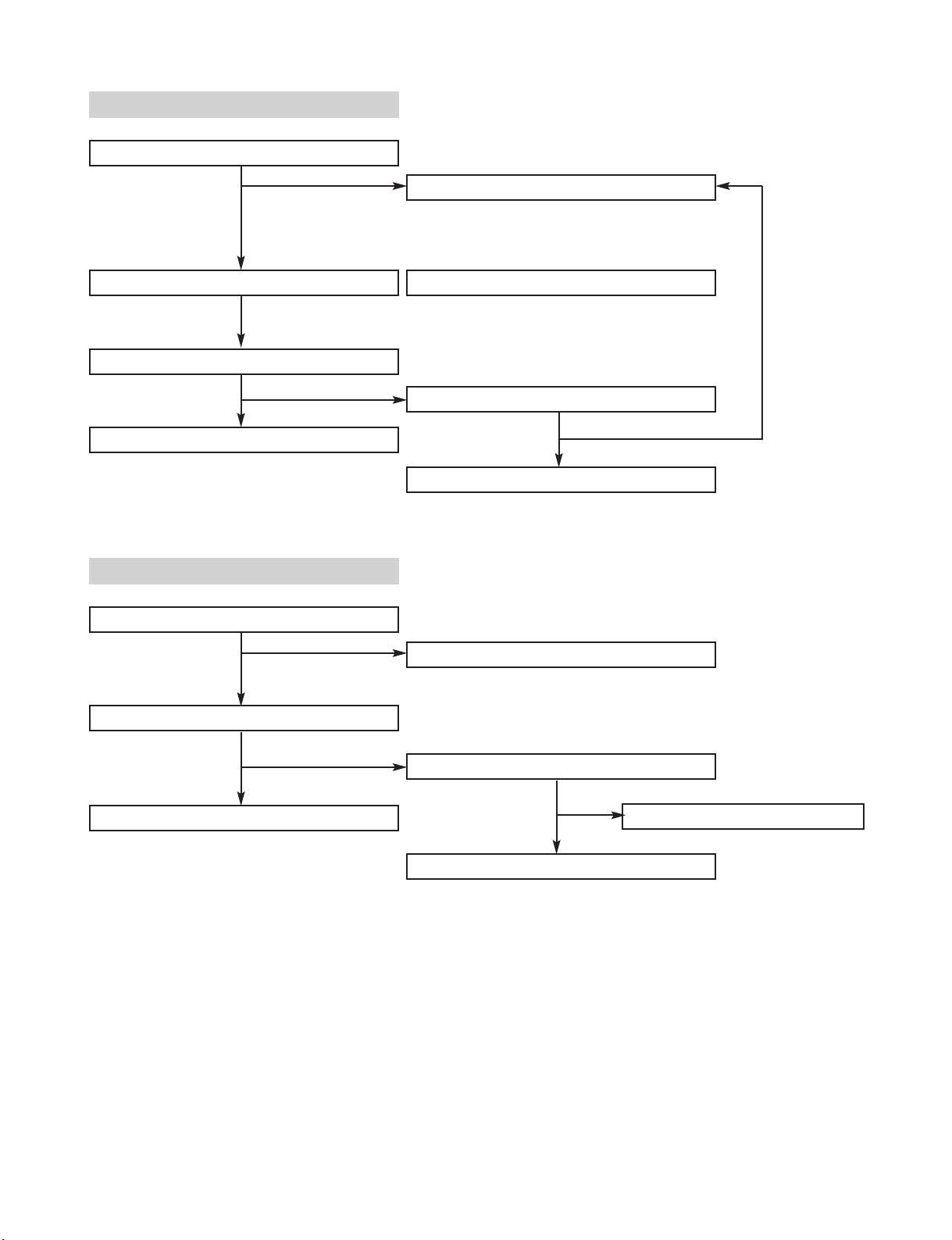
IC301 U-COM IC Troubleshooting
IC301 pin17, 46, 72, 90 +5V power check
IC301 PIN26 5V check (POWER-SENS)
X301 oscilates or not
When IC301 pin11 voltage input Low➞High
IC301 replacement
CN302 PIN6 DC +5.6V check
PATTERN check
Troubleshooting Refer
P-SENS refer
X301 replacement
RESET circuit check
YES
YES
YES
YES
YES
NO
NO
NO
NO
NO
IC501(EXPENDER IC) Troubleshooting
IC501
PIN
16 +5V power check
IC501 PIN2, 3 pin CLK Data check
CONTROLL function check
normal
Troubleshooting Refer
IC301 TROUBLESHOOTING refer
IC301, IC501 pattern check
IC301 PIN3, 4 Data check (CD, TAPE FUNCTION change)
IC501(BU2090F) replacement
YES
YES
YES
YES
NO
NO
NO
NO
Page 14
- 2-9 -
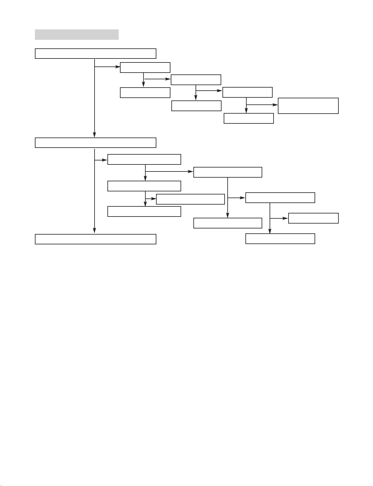
IC700(AMP IC) Troubleshooting
PIN
10, 14 Signal input check
2(+VH2), 1(-VH2) power check
PIN3, 4, 5, 6 signal output check
OK
Muting circuit refer
PIN3, 4, 5, 6 DC check
Power IC replacement
Power IC replacement
YES
YES
YES
YES
NO
NO
TAPE PLAY
IC202 “18”pin VCC check
IC202 “5, 20”pin signal output check
Muting circuit check
Troubleshooting check refer
Deck Mecha operation check
IC202 replaement
Deck Mecha replaement
YES
YES
YES
NO
NO
NO
Page 15
- 2-10 -
IC501 Troubleshooting refer
TAPE REC check (A252, Q202 On: R273, R223 High
IC202
PIN
11, 14 signal input check
IC202
PIN
9, 16 output check
IC201 ‘6”(12V) ,
PIN
4 High check
L203
PIN
5, 6 oscilates or not
DECK replaement
Q253, Q203 Base “Low” check
Q253, Q203
replaement
IC202 PIN18 VCC check
IC501 Troubleshooting check
C236(+) power input check
Troubleshooting check refer
IC501 Troubleshooting check
Q208
replaement
L203
replaement
Q208 Base 0.6V check
Q208 Collector Low
Q207
replaement
normal
YES
YES
YES
YES
YES
YES
YES
YES
YES
NO
NO
NO
NO
NO
NO
NO
NO
NO
Dubbing check (“NORMAL”or “HIGH”) check
Q252, 202 “OFF”//”ON”: R273, 223 “LOW”// “HIGH”
Q253, 203 “OFF”//”ON”: R225, 275 “LOW”// “HIGH” IC501 Troubleshooting check
REC check refer
YES
YES
NO
Page 16
❏ BLOCK DIAGRAM
2-11 2-12
Page 17
2-13 2-14
❏ SCHEMATIC DIAGRAMS
• MAIN SCHEMATIC DIAGRAM
Page 18
2-15 2-16
• MAIN(AMP), SUB POWER SCHEMATIC DIAGRAM
Page 19
2-17 2-18
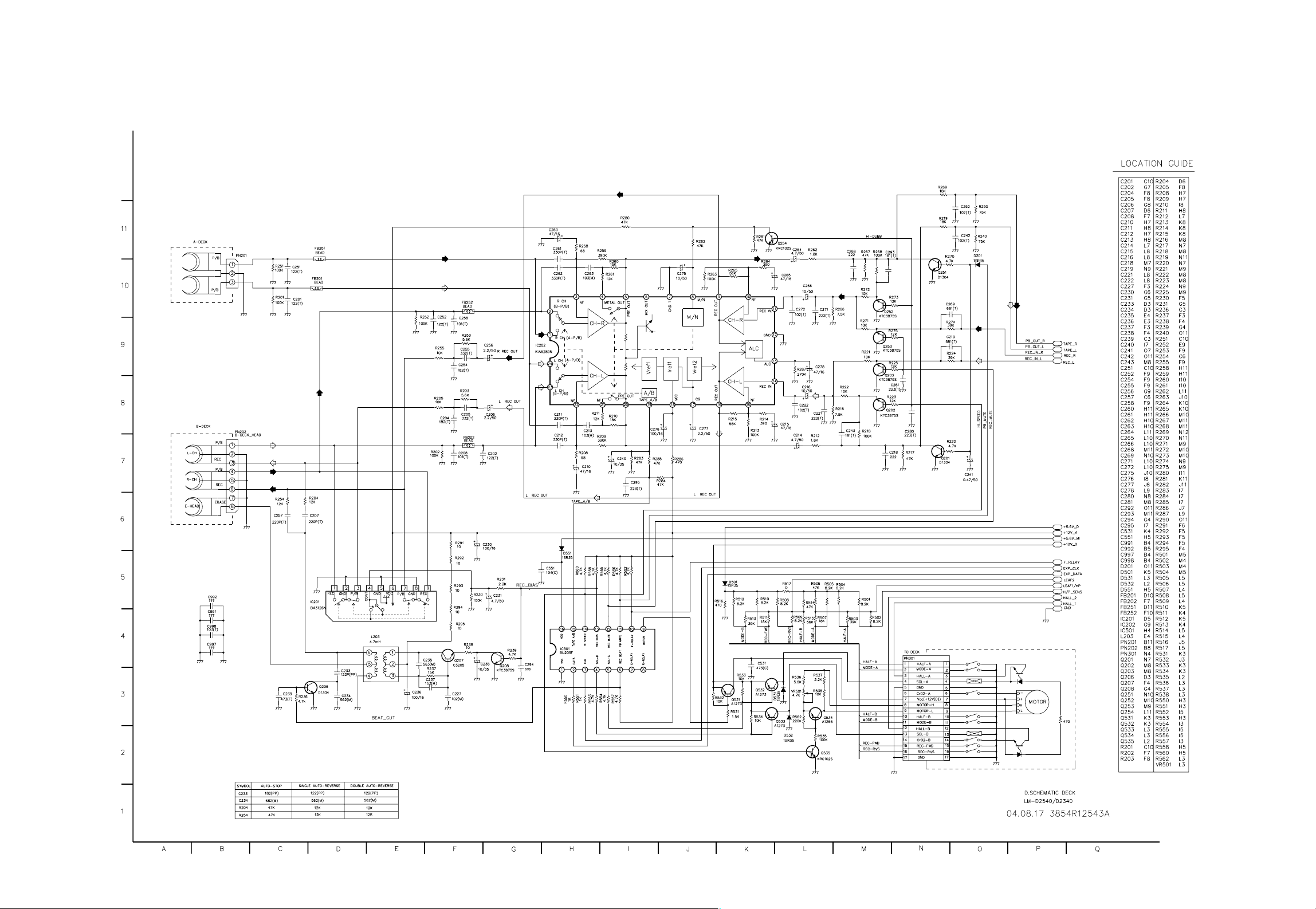
• MAIN(DECK) SCHEMATIC DIAGRAM
Page 20
2-19 2-20
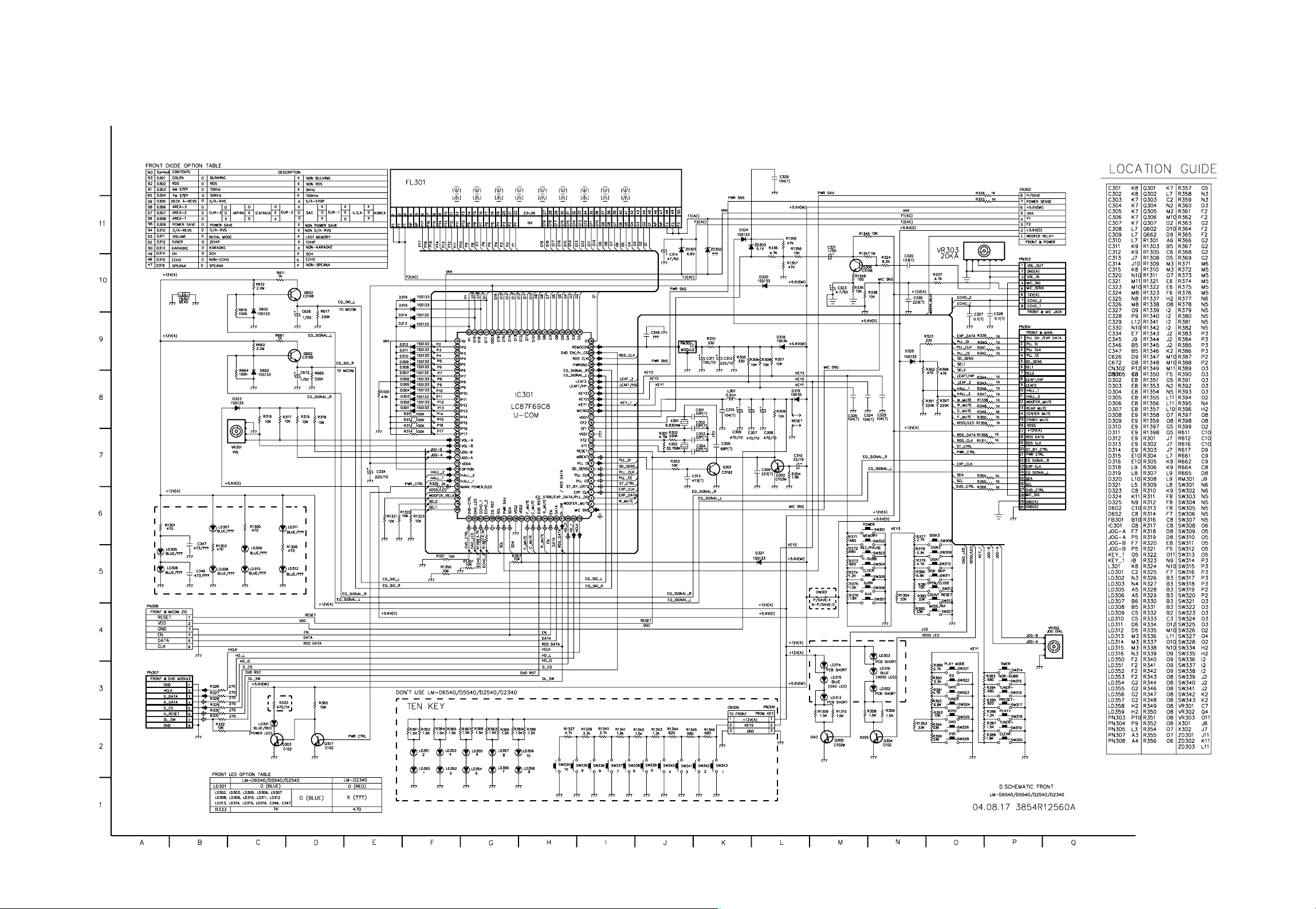
• FRONT SCHEMATIC DIAGRAM
Page 21
2-21 2-22
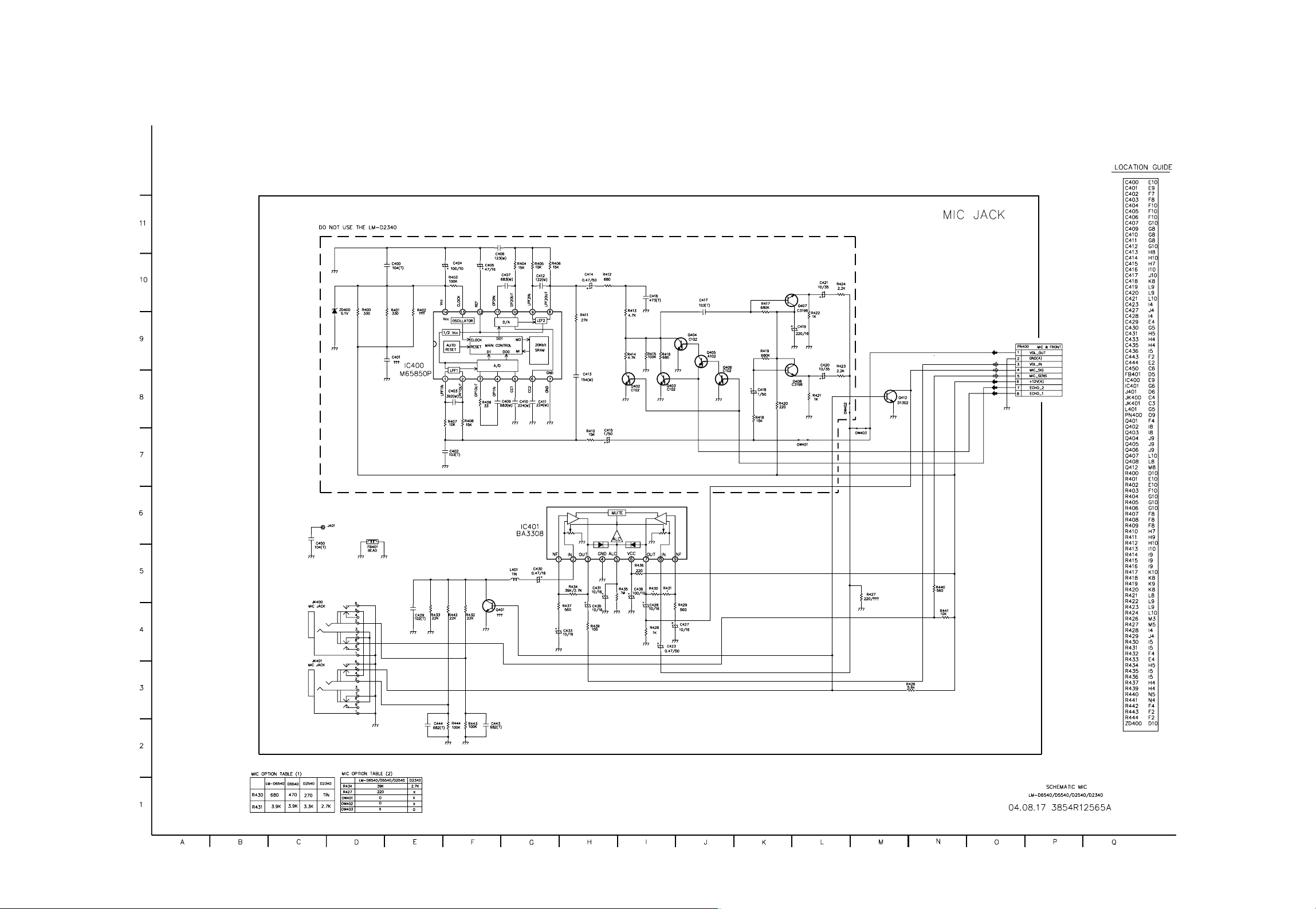
• MIC SCHEMATIC DIAGRAM
Page 22
2-23 2-24
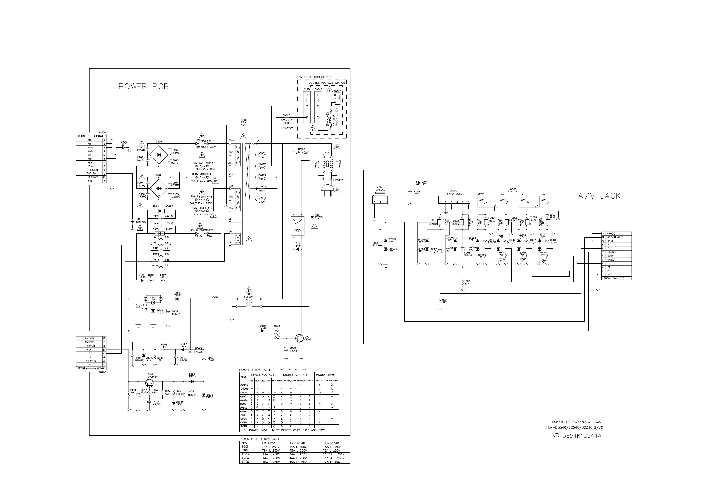
• POWER, A/V JACK SCHEMATIC DIAGRAM
Page 23

2-25 2-26
• POWER, A/V JACK SCHEMATIC DIAGRAM
Page 24

2-27 2-28
❏ WIRING DIAGRAM
Page 25

2-29 2-30
❏ PRINTED CIRCUIT DIAGRAMS
• MAIN P.C. BOARD (SOLDER SIDE)
Page 26

2-31 2-32
• MAIN P.C. BOARD (COMPONENT SIDE)
Page 27

2-33 2-34
• FRONT P.C. BOARD (SOLDER SIDE)
Page 28

2-35 2-36
• FRONT P.C. BOARD (COMPONENT SIDE)
Page 29

2-37 2-38
• POWER P.C. BOARD (COMPONENT SIDE)
Page 30

2-39 2-40
• POWER P.C. BOARD (SOLDER SIDE)
Page 31

2-41 2-42
• POWER P.C. BOARD (SOLDER SIDE)
• POWER P.C. BOARD (COMPONENT SIDE)
• FAN ZIG P.C. BOARD
• DOUBLE VOLTAGE P.C. BOARD
Page 32

2-43 2-44
• A/V JACK P.C. BOARD (SOLDER SIDE) • A/V JACK P.C. BOARD (COMPONENT SIDE)
Page 33

2-45 2-46
Page 34

- 3-1 -
SECTION 3. DVD PART
❏ DVD ELECTRICAL TROUBLESHOOTING GUIDE
1. Power check flow
Page 35

- 3-2 -
2. Test & debug flow
Page 36

- 3-3 -
Page 37

- 3-4 -
Page 38

- 3-5 -
Page 39

- 3-6 -
Page 40

- 3-7 -
❏ INTERNAL BLOCK DIAGRAM of ICs
• ES6603 (IC401)
BLOCK DIAGRAM
Page 41

- 3-8 -
Page 42

- 3-9 -
Page 43

- 3-10 -
Page 44

- 3-11 -
• BA5954FM (IC404)
BLOCK DIAGRAM
Page 45

- 3-12 -
• ES6698 (IC501)
BLOCK DIAGRAM
Page 46

- 3-13 -
Page 47

- 3-14 -
Page 48

- 3-15 -
Page 49

- 3-16 -
Page 50

- 3-17 -
Page 51

- 3-18 -
Page 52

- 3-19 -
Page 53

- 3-20 -
Page 54

- 3-21 -
Page 55

- 3-22 -
❏ DVD BLOCK DIAGRAM
• ESS 3-CHANGER SYSTEM BLOCK DIAGRAM
Page 56

- 3-23 -
• ESS 3-CHANGER MEMORY & HOST I/F BLOCK DIAGRAM
Page 57

- 3-24 -
• ESS 3-CHANGER SERVO & MOTOR BLOCK DIAGRAM
Page 58

- 3-25 -
• ESS 3-CHANGER A/V SYSTEM BLOCK DIAGRAM
Page 59

- 3-26 -
❏ REPAIRS REGARDING CD MECHANISM
•
IMPROVED MECHOD-WHEN THE TRAY GEARS WERE DISTORTED
PIC K U P
GEAR MAIN
BASE MAIN
TRAY LOADING
GEAR CAM
H
GEAR PU DOWN
H
1. How to open the tray
Push two hooks (H) of the BASE MAIN, and open the TRAY LOADING
2. How to correct the distorted gears
(1) Turn GEAR MAIN until it clicks, if so that PICK-UP is downed completely
(2) The hold of GEAR FU DOWN array as the arrow of BASENAIN
(3) Push the TRAY LOADING
Page 60

3-27 3-28
❏ SCHEMATIC DIAGRAMS
• MPEG SCHEMATIC DIAGRAM
Page 61

3-29 3-30
• RF & SERVO SCHEMATIC DIAGRAM
Page 62

3-31 3-32
• I/O SCHEMATIC DIAGRAM
Page 63

3-33 3-34
❏ PRINTED CIRCUIT DIAGRAMS
• MAIN P.C. BOARD (SOLDER SIDE)
Page 64

3-35 3-36
• MAIN P.C. BOARD (COMPONENT SIDE)
Page 65

4-1 4-2
SECTION 4. EXPLODED VIEWS
458
302
458
A46
301
A47
A48
300
305
291
457
292
278
277
454
276
275
FAN
456
272
454
A41
271
A26
A00
A43
264
459
A50
263
454
262
261
260
265
259
256
255
257
258
252
266
451
270
250
251
253
254
290
454
❏ CABINET AND MAIN FRAME SECTION
Page 66

❏ TAPE DECK MECHANISM (A/R & A/S : LEFT A/S DECK)
016
401
018
007
008
015
023
019
021
020
505
017
403
504
025
026
030
029
028
401
027
502
009
401
003
501
401
011
013
009
022
4-3 4-4
LOCA. NO. LG PART NO. DESCRIPTION SPECIFICATION
A00 6720AG0002C DECK,AUDIO CWM42FR47 TOKYO PIGEON L-DOUBL
003 6768R-PP03A DECK MECHANISM PARTS 33-160-4309 PIGEON PRESS CASSE
007 6768R-GP03B DECK MECHANISM PARTS 50-222-4578 PIGEON GEAR IDLER
008 6768R-SP01F DECK MECHANISM PARTS 01-082-4598 PIGEON SPRING CWL4
009 6768R-MP01C DECK MECHANISM PARTS 50-219-4014 PIGEON MOLD CWL44
011 6768R-SP01A DECK MECHANISM PARTS 01-081-4601 PIGEON SPRING CWL4
013 6768R-SP03A DECK MECHANISM PARTS 01-082-4686 PIGEON SPRING CRM4
015 6768R-AP01A DECK MECHANISM PARTS 50-268-3016 PIGEON ARM CWL44
016 6768R-GP01H DECK MECHANISM PARTS 50-093-4503 PIGEON GEAR CRL442
017 6768R-AP01C DECK MECHANISM PARTS 50-239-4072 PIGEON ARM CWL44
018 6768R-GP01J DECK MECHANISM PARTS 50-222-4428 PIGEON GEAR CRL442
019 6768R-SP01P DECK MECHANISM PARTS 01-081-4678 PIGEON SPRING CRL4
020 6768R-BP01C DECK MECHANISM PARTS 02-083-4188 PIGEON BELT/FELT C
021 6768R-LP01C DECK MECHANISM PARTS 50-223-4429 PIGEON PULLEY/FLYW
022 6768R-VP03A DECK MECHANISM PARTS 50-093-4748 PIGEON SOLENOID AS
023 6768R-GP03A DECK MECHANISM PARTS 50-093-4810 PIGEON GEAR ASSY C
025 6768R-JP03B DECK MECHANISM PARTS 50-093-31009 PIGEON PULLEY/FLY
026 6768R-SP01D DECK MECHANISM PARTS 01-080-4609 PIGEON SPRING CWL4
027 6768R-DP01A DECK MECHANISM PARTS 50-259-3342 PIGEON LEVER CWL44
028 6768R-RP01A DECK MECHANISM PARTS 22-027-41054 PIGEON ROLLER CWL
029 6768R-MP01A DECK MECHANISM PARTS 50-219-4033 PIGEON MOLD CWL44
030 6768R-EP03C DECK MECHANISM PARTS T21V0P PIGEON HEAD CWM42FF30
401 6768R-CP01B DECK MECHANISM PARTS GSE20A2005 PIGEON SCREW CWL44
403 6768R-CP01D DECK MECHANISM PARTS GSL10A1704 PIGEON SCREW CWL44
501 6768R-WP03A DECK MECHANISM PARTS GWN19S035040 PIGEON WASHER CRM
502 6768R-WP03B DECK MECHANISM PARTS 03-000-4532 PIGEON WASHER CRM4
504 6768R-WP01D DECK MECHANISM PARTS GWP21X045020 PIGEON WASHER CWL
505 6768R-WP01E DECK MECHANISM PARTS GWP12X030040S PIGEON WASHER CW
Page 67

4-5 4-6
❏ TAPE DECK MECHANISM (A/R & A/S : RIGHT A/R DECK)
025
504
023
015
022
019
037
021
020
505
018
017
016
506
006
A01
402
008
007
401
001
002
003
502
507
501
502
402
401
009
401
009
011
013
035
039
031
040
028
029
027
026
038
028
032
406
409
403
036
LOCA. NO. LG PART NO. DESCRIPTION SPECIFICATION
A00 6720AG0002C DECK,AUDIO CWM42FR47 TOKYO PIGEON L-DOUBL
A01 6768R-UP03D DECK MECHANISM PARTS 50-093-4895 PIGEON PWB UNIT CW
001 6768R-BP03D DECK MECHANISM PARTS 02-083-4254 PIGEON BELT/FELT C
002 6768R-BP03E DECK MECHANISM PARTS 02-083-4256 PIGEON BELT/FELT C
003 6768R-PP03A DECK MECHANISM PARTS 33-160-4309 PIGEON PRESS CASSE
006 6768R-QP03C DECK MECHANISM PARTS 50-093-4880 PIGEON MOTOR(ASSY)
007 6768R-GP03B DECK MECHANISM PARTS 50-222-4578 PIGEON GEAR IDLER
008 6768R-SP01F DECK MECHANISM PARTS 01-082-4598 PIGEON SPRING CWL4
009 6768R-MP01C DECK MECHANISM PARTS 50-219-4014 PIGEON MOLD CWL44
011 6768R-SP01A DECK MECHANISM PARTS 01-081-4601 PIGEON SPRING CWL4
013 6768R-SP03A DECK MECHANISM PARTS 01-082-4686 PIGEON SPRING CRM4
015 6768R-AP01A DECK MECHANISM PARTS 50-268-3016 PIGEON ARM CWL44
016 6768R-GP01H DECK MECHANISM PARTS 50-093-4503 PIGEON GEAR CRL442
017 6768R-AP01C DECK MECHANISM PARTS 50-239-4072 PIGEON ARM CWL44
018 6768R-GP01J DECK MECHANISM PARTS 50-222-4428 PIGEON GEAR CRL442
019 6768R-SP01P DECK MECHANISM PARTS 01-081-4678 PIGEON SPRING CRL4
020 6768R-BP01C DECK MECHANISM PARTS 02-083-4188 PIGEON BELT/FELT C
021 6768R-LP01C DECK MECHANISM PARTS 50-223-4429 PIGEON PULLEY/FLYW
022 6768R-VP03A DECK MECHANISM PARTS 50-093-4748 PIGEON SOLENOID AS
023 6768R-GP03A DECK MECHANISM PARTS 50-093-4810 PIGEON GEAR ASSY C
025 6768R-JP03B DECK MECHANISM PARTS 50-093-31009 PIGEON PULLEY/FLY
026 6768R-SP01D DECK MECHANISM PARTS 01-080-4609 PIGEON SPRING CWL4
027 6768R-DP01A DECK MECHANISM PARTS 50-259-3342 PIGEON LEVER CWL44
028 6768R-RP01A DECK MECHANISM PARTS 22-027-41054 PIGEON ROLLER CWL
029 6768R-MP01A DECK MECHANISM PARTS 50-219-4033 PIGEON MOLD CWL44
031 6768R-SP04A DECK MECHANISM PARTS 01-082-4731 PIGEON SPRING
032 6768R-EP04A DECK MECHANISM PARTS 50-093-41007 PIGEON HEAD ASSY
035 6768R-PP04A DECK MECHANISM PARTS 50-119-4915 PIGEON PRESS
036 6768R-SP04B DECK MECHANISM PARTS 01-081-4730 PIGEON SPRING
037 6768R-JP03A DECK MECHANISM PARTS 50-093-4674 PIGEON PULLEY/FLYW
038 6768R-MP01D DECK MECHANISM PARTS 50-219-4034 PIGEON MOLD CWL44
039 6768R-MP02A DECK MECHANISM PARTS 50-219-3900 PIGEON MOLD
040 6768R-SP01M DECK MECHANISM PARTS 01-080-4607 PIGEON SPRING CWL4
401 6768R-CP01B DECK MECHANISM PARTS GSE20A2005 PIGEON SCREW CWL44
402 6768R-CP01A DECK MECHANISM PARTS GSE10A2003 PIGEON SCREW CWL44
403 6768R-CP01D DECK MECHANISM PARTS GSL10A1704 PIGEON SCREW CWL44
406 6768R-CP01G DECK MECHANISM PARTS GSE20A2004 PIGEON SCREW CWL44
409 6768R-CP02A DECK MECHANISM PARTS GSD10A2016 PIGEON SCREW
501 6768R-WP03A DECK MECHANISM PARTS GWN19S035040 PIGEON WASHER CRM
502 6768R-WP03B DECK MECHANISM PARTS 03-000-4532 PIGEON WASHER CRM4
504 6768R-WP01D DECK MECHANISM PARTS GWP21X045020 PIGEON WASHER CWL
505 6768R-WP01E DECK MECHANISM PARTS GWP12X030040S PIGEON WASHER CW
506 6768R-WP01H DECK MECHANISM PARTS GWP23X040020 PIGEON WASHER CWL
507 6768R-WP01F DECK MECHANISM PARTS GWN21X040040 PIGEON WASHER CWL
Page 68

❏ DECK MECHANISM EXPLODED VIEWS
416
151
156
418
169
173
419
163
422
165
159
164
417
417
416
166
167
177
175
172
162
153
168
155
417
417
A30
A35
185
171
170
421
184
421
184
421
184
421
184
LOCA.NO PART NO DESCRIPTION SPECIFICATION
A26 4405RCS006E MECHANISM ASSEMBLY DVM-H1513 HZ(DP-8-VE)DVD 3
A30 3041RBD003C BASE ASSEMBLY PU (DVM-H1513 DP-8-VE) HZ
A35 3041R-M016L BASE ASSEMBLY SLED(DP-8-VE) HZ
151 3390RB0002A TRAY DISC(CDM-H1503)
153 4470RB0005A GEAR TRAY (CDM-H1503)
155 4681RBA001B MOTOR ASSEMBLY HOME TRAY (CDM-H1503) MABUCHI
156 6871RF9211A PWB(PCB) ASSEMBLY,FRONT 1503 T/D SENSOR
159 3390RB0001A TRAY LOADING(CDM-H1503)
162 4400SB0001A BELT AUDIO MAIN(CDM-H1303)
163 4470SB0003A GEAR PULLEY (CDM-H1303)
164 4470RB0003A GEAR LOADING (CDM-H1503)
165 6871RZ7036A PWB(PCB) ASSEMBLY,OTHERS CDM-H1503 UP/DW/OP/CL
166 4470RB0006A GEAR PU UP (CDM-H1503)
167 4470RB0007A GEAR PU DOWN (CDM-H1503)
168 4470RB0002A GEAR CAM (CDM-H1503)
170 3300R-0547A PLATE CLAMP
171 5016H-1016B MAGNET CLAMP(LDM-R608,10*5,1*1.5T)"
172 3040RB0005A BASE MAIN (CDM-H1503)
173 4510RB0001A LEVER S/W CLOSE
175 4680SBP001A MOTOR(MECH) OTHER . . .
177 4470RB0001A GEAR MAIN (CDM-H1503)
184 5040R-0075D RUBBER DAMPER DP7 (YAMAUCHI 30)
185 3040RBM001A BASE PU MOLD (DVM-H1513)
416 88H-0004 CD MECHA PARTS 3X12X12FNM
417 88H-0002 CD MECHA PARTS 3X9X12FZMY
418 353-025BAAA SCREW,DRAWING #NAME?
419 88H-0003 CD MECHA PARTS 3X12X10FZMY
420 353S353F SCREW,DRAWING #NAME?
421 1SZZH-1003A SCREW,DRAWING + D2.0 6MM SWRCH16A/NIY 4.5MM
422 353-028H SCREW #NAME?
4-7 4-8
Page 69

Page 70

- 5-1 -
SECTION 5. SPEAKER PART
843
LEFT
844
RIGHT
LEFT
RIGHT
842
841
838
839
840
837
836
833
835
834
834
832
830
831
❏ MODEL : LMS-D2540V
LOCA.NO. PART NO DESCRIPTION SPECIFICATION REMARKS
830 3720RMF106A PANEL,FRONT SPK LMS-D6540V MOLD FRONT PANE
831 3720RMF107A PANEL,FRONT SPK LMS-D6540V MOLD RIGHT FRON
832 353M050C SCREW,DRAWING BH 3.5X16 FBK
833 6400RMXY01A SPEAKER,GENERAL (FE-376E) PIEZO LG 0OHM 0W 0DB
834 353M025F SCREW,DRAWING TAPTITE, 3X8 FZMY
835 6400TSMA02A SPEAKER,TWEETER CTR-50B55L SAMMI TWEETER(CONE)
836 353M050M SCREW,DRAWING + 2 D3.5 L10.0 MSWR3/FZY
837 6400WSMJ07A SPEAKER,WOOFER CW-165B55L SAMMI WOOFER 6OHM 5
839 4350RM0013A RING SPK LMS-D6540V MOLD WOOFER RIN
840 4766RM0158A FELT LMS-D6540V BLACK FOR DUCT1
841 4766RM0159A FELT LMS-D6540V BLACK FOR DUCT2
842 3610RM0051A FOOT SPK LFS-K5930V OTHER PHI 20 X
843 3091RMW125A CABINET ASSEMBLY SPK LMS-D6540V CABINET ASSY
844 3091RMW125B CABINET ASSEMBLY SPK LMS-D6540V RIGHT CABINET A
Page 71

- 5-2 -
 Loading...