

Page 1

- 1-1 -
[CONTENTS]
SECTION 1.GENERAL
• SERVICING PRECAUTIONS ................................................................................................ 1-2
• ESD PRECAUTIONS............................................................................................................. 1-4
• SPECIFICATIONS...................................................................................................................1-5
SECTION 2. ELECTRICAL
• AUDIO TROUBLESHOOTING GUIDE .................................................................................. 2-1
• DVD TROUBLESHOOTING GUIDE ...................................................................................... 2-5
• DVD DETAILS AND WAVEFORMS ON SYSTEM TESTAND DEBUGGING..................... 2-13
• WIRING DIAGRAM.............................................................................................................. 2-25
• BLOCK DIAGRAMS............................................................................................................. 2-26
• AUDIO PART SCHEMATIC DIAGRAMS ............................................................................. 2-31
• DVD PART SCHEMATIC DIAGRAMS................................................................................. 2-47
• PRINTED CIRCUIT DIAGRAMS ......................................................................................... 2-53
• CIRCUIT VOLTAGE CHART................................................................................................ 2-63
SECTION 3. EXPLODED VIEWS
• CABINET AND MAIN FRAME SECTION .............................................................................. 3-1
• DECK MECHANISM EXPLODED VIEW .............................................................................. 3-3
• PACKING ACCESSOR Y SECTION ...................................................................................... 3-5
SECTION 4. SPEAKER PART .................................................................................. 4-1
SECTION 5. REPLACEMENT PARTS LIST ............................................................. 5-1
Page 2
- 1-2 -
SECTION 1. GENERAL
SERVICING PRECAUTIONS
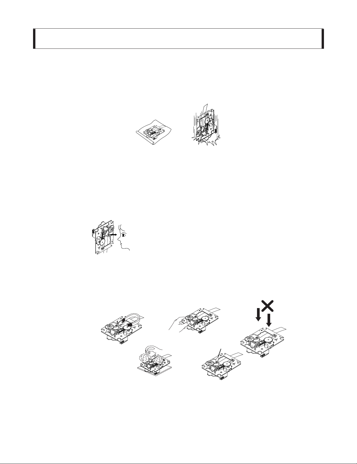
NOTES REGARDING HANDLING OF THE PICK-UP
1. Notes for transport and storage
1) The pick-up should always be left in its conductive bag until immediately prior to use.
2) The pick-up should never be subjected to external pressure or impact.
2. Repair notes
1) The pick-up incorporates a strong magnet, and so should never be brought close to magnetic materials.
2) The pick-up should always be handled correctly and carefully, taking care to avoid external pressure and
impact. If it is subjected to strong pressure or impact, the result may be an operational malfunction and/or
damage to the printed-circuit board.
3) Each and every pick-up is already individually adjusted to a high degree of precision, and for that reason
the adjustment point and installation screws should absolutely never be touched.
4) Laser beams may damage the eyes!
Absolutely never permit laser beams to enter the eyes!
Also NEVER switch ON the power to the laser output part (lens, etc.) of the pick-up if it is damaged.
5) Cleaning the lens surface
If there is dust on the lens surface, the dust should be cleaned away by using an air bush (such as used
for camera lens). The lens is held by a delicate spring. When cleaning the lens surface, therefore, a cotton swab should be used, taking care not to distort this.
6) Never attempt to disassemble the pick-up.
Spring by excess pressure. If the lens is extremely dirty, apply isopropyl alcohol to the cotton swab.
(Do not use any other liquid cleaners, because they will damage the lens.) Take care not to use too much
of this alcohol on the swab, and do not allow the alcohol to get inside the pick-up.
Storage in conductive bag
Drop impact
NEVER look directly at the laser beam, and don’t let
contact fingers or other exposed skin.
Magnet
How to hold the pick-up
Conductive Sheet
Cotton swab
Pressure
Pressure
Page 3
- 1-3 -
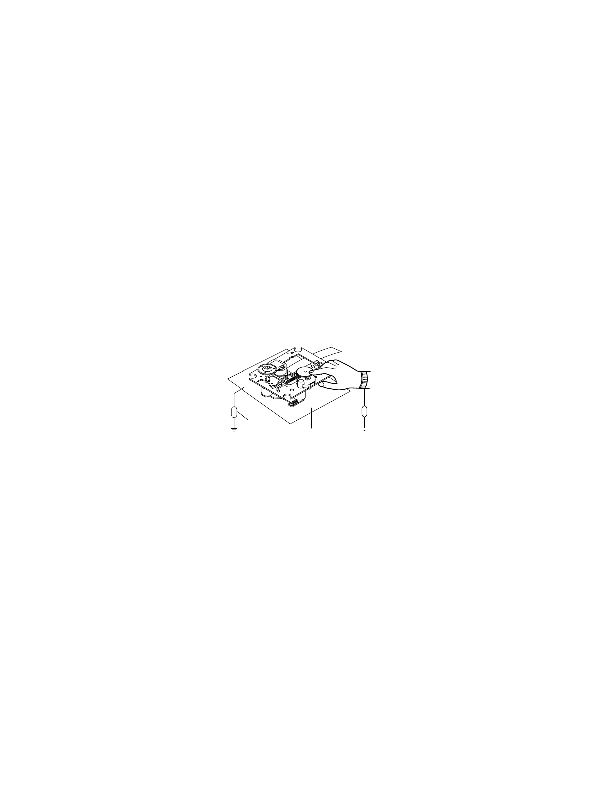
NOTES REGARDING COMPACT DISC PLAYER REPAIRS
1. Preparations
1) Compact disc players incorporate a great many ICs as well as the pick-up (laser diode). These components
are sensitive to, and easily affected by, static electricity. If such static electricity is high voltage, components
can be damaged, and for that reason components should be handled with care.
2) The pick-up is composed of many optical components and other high-precision components. Care must be
taken, therefore, to avoid repair or storage where the temperature of humidity is high, where strong magnetism is present, or where there is excessive dust.
2. Notes for repair
1) Before replacing a component part, first disconnect the power supply lead wire from the unit
2) All equipment, measuring instruments and tools must be grounded.
3) The workbench should be covered with a conductive sheet and grounded.
When removing the laser pick-up from its conductive bag, do not place the pick-up on the bag. (This is
because there is the possibility of damage by static electricity.)
4) To prevent AC leakage, the metal part of the soldering iron should be grounded.
5) Workers should be grounded by an armband (1M Ω)
6) Care should be taken not to permit the laser pick-up to come in contact with clothing, in order to prevent
static electricity changes in the clothing to escape from the armband.
7) The laser beam from the pick-up should NEVER be directly facing the eyes or bare skin.
Resistor
(1 Mohm)
Conductive
Sheet
Resistor
(1 Mohm)
Armband
Page 4
- 1-4 -
ESD PRECAUTIONS
Electrostatically Sensitive Devices (ESD)
Some semiconductor (solid state) devices can be damaged easily by static electricity. Such components
commonly are called Electrostatically Sensitive Devices (ESD). Examples of typical ESD devices are integrated
circuits and some field-effect transistors and semiconductor chip components. The following techniques should
be used to help reduce the incidence of component damage caused by static electricity.
1. Immediately before handling any semiconductor component or semiconductor-equipped assembly, drain off
any electrostatic charge on your body by touching a known earth ground. Alternatively, obtain and wear a
commercially available discharging wrist strap device, which should be removed for potential shock reasons
prior to applying power to the unit under test.
2. After removing an electrical assembly equipped with ESD devices, place the assembly on a conductive sur-
face such as aluminum foil, to prevent electrostatic charge buildup or exposure of the assembly.
3. Use only a grounded-tip soldering iron to solder or unsolder ESD devices.
4. Use only an anti-static solder removal device. Some solder removal devices not classified as "anti-static" can
generate electrical charges sufficient to damage ESD devices.
5. Do not use freon-propelled chemicals. These can generate electrical charges sufficient to damage ESD
devices.
6. Do not remove a replacement ESD device from its protective package until immediately before you are
ready to install it. (Most replacement ESD devices are packaged with leads electrically shorted together by
conductive foam, aluminum foil or comparable conductive materials).
7. Immediately before removing the protective material from the leads of a replacement ESD device, touch the
protective material to the chassis or circuit assembly into which the device will by installed.
CAUTION : BE SURE NO POWER IS APPLIED TO THE CHASSIS OR CIRCUIT, AND OBSERVE ALL
OTHER SAFETY PRECAUTIONS.
8. Minimize bodily motions when handing unpackaged replacement ESD devices. (Otherwise harmless motion
such as the brushing together of your clothes fabric or the lifting of your foot from a carpeted floor can generate static electricity sufficient to damage an ESD device).
CAUTION. GRAPHIC SYMBOLS
THE LIGHTNING FLASH WITH APROWHEAD SYMBOL. WITHIN AN EQUILATERAL TRIANGLE, IS
INTENDED TO ALERT THE SERVICE PERSONNELTO THE PRESENCE OF UNINSULATED “DANGEROUS VOLTAGE” THAT MAY BE OF SUFFICIENT MAGNITUDE TO CONSTITUTE ARISK OF
ELECTRIC SHOCK.
THE EXCLAMATION POINTWITHIN AN EQUILATERAL TRIANGLE IS INTENDED TO ALERT THE
SERVICE PERSONNEL TO THE PRESENCE OF IMPORTANTSAFETY INFORMATION IN SERVICE
LITERATURE.
Page 5

- 1-5 -
SPECIFICATIONS
GENERAL
Power supply Refer to main label
Power consumption Refer to main label
Mass 5.5 kg
External dimensions (W x H x D) 435 x 54 x 350 mm
Operating conditions Temperature: 5°C to 35°C, Operation status: Horizontal
Operating humidity 5% to 85%
CD/DVD
Laser Semiconductor laser, wavelength 650 nm
Signal system NTSC 525/60
Frequency response (audio) 150 Hz to 18 kHz
Signal-to-noise ratio (audio) More than 75 dB (1 kHz, NOP -6 dB, 20 kHz LPF/A-Filter)
Dynamic range (audio) More than 70 dB
Harmonic distortion (audio) 0.5 % (1 kHz, at 1W position) (20 kHz LPF)
VIDEO
Video input 1.0 V (p-p), 75 Ω, negative sync., RCA jack x 2
Video output 1.0 V (p-p), 75 Ω, negative sync., RCA jack x 1
S-video output (Y) 1.0 V (p-p), 75 Ω, negative sync., Mini DIN 4-pin x 1
(C) 0.3 V (p-p), 75 Ω
COMPONENT VIDEO OUT (Y) 1.0 V (p-p), 75 ohms, negative sync, RCA jack x 1
(Pb)/(Pr) 0.7 V (p-p), 75 ohms, RCA jack x 2
TUNER
FM
Tuning Range 87.5 - 108.0 MHz or 65.0 - 74.0 MHz, 87.5 - 108.0 MHz
Intermediate Frequency 10.7 MHz
Signal-to Noise Ratio 60 dB (Mono)
Frequency Response 150 - 8,000 Hz
AM[MW]
Tuning Range 520 - 1,720 kHz
Intermediate Frequency 450 kHz
AMPLIFIER
Stereo mode 150W + 150W (6Ω at 1 kHz, THD 10 %)
Surround mode Front: 150W + 150W (THD 10 %)
Center*: 150W
Surround*: 150W + 150W (6Ω at 1 kHz, THD 10 %)
Subwoofer*: 250W (4Ω at 30 Hz, THD 10 %)
SPEAKERS
Front/Rear Speaker Center speaker Passive Subwoofer
(LHS-75SGS) (LHS-75SGC) (LHS-75SGW)
Type 2 Way 2 Speaker 2 Way 2 Speaker 1 Way 1 Speaker
Impedance 6 Ω 6 Ω 4 Ω
Frequency Response 145 - 20,000 Hz 120 - 20,000 Hz 50 - 1,500 Hz
Sound Pressure Level 85 dB/W (1m) 85 dB/W (1m) 83 dB/W (1m)
Rated Input Power 150 W 150 W 250 W
Max. Input Power 300 W 300 W 500 W
Net Dimensions (W x H x D) 104 x 235 x 120 mm 220 x 115 x 120 mm 195 x 398 x 419 mm
Net Weight 1.0kg 1.0kg 6.6kg
(* Depending on the sound mode
settings and the source, there may
be no sound output.)
Page 6
- 2-1 -
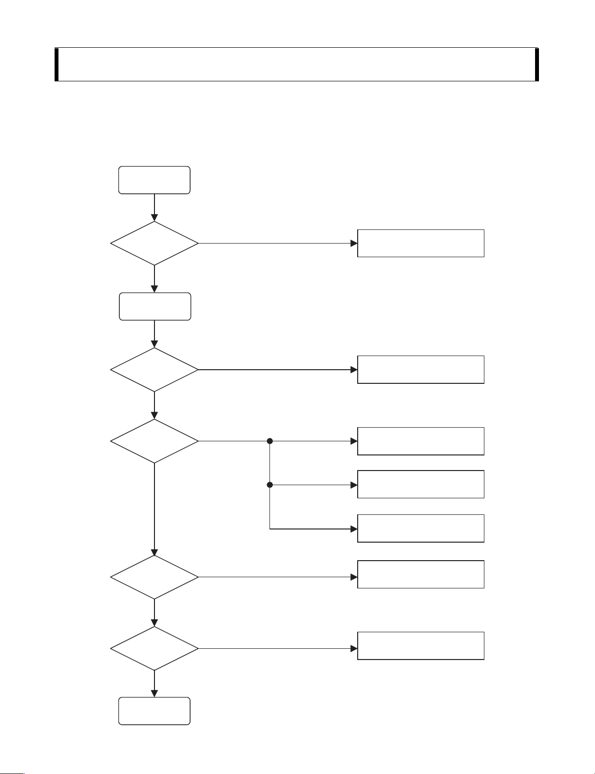
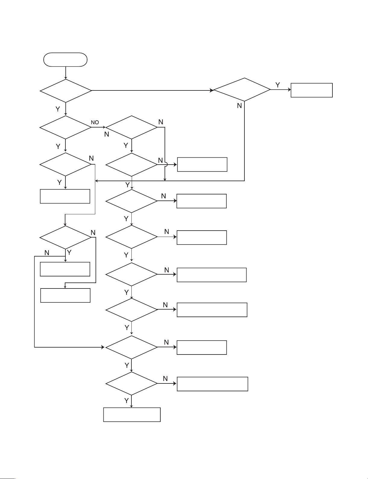
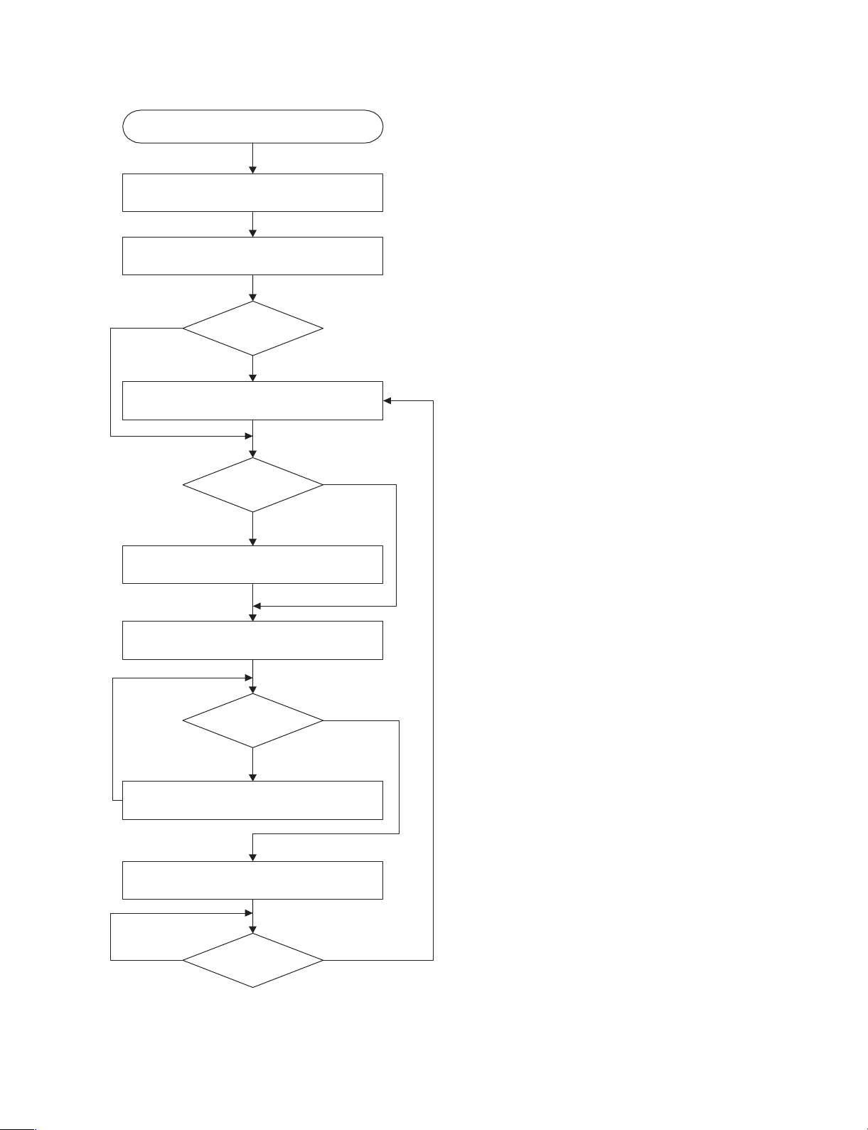
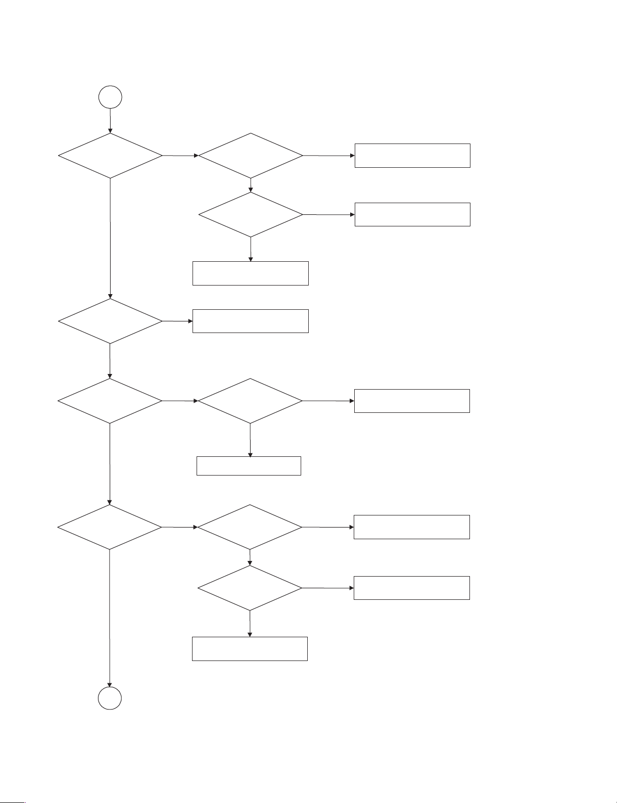
AUDIO TROUBLESHOOTING GUIDE
1. POWER CHECK FLOW
SECTION 2. ELECTRICAL
INSERT
WER CORD.
PO
TURN ON
THE RED LED?
YES
TURN PO
IS PO
WER ON.
WER ON?
YES
DOES INITIAL
WORK?
READ
YES
NO
NO
NO
CHECK POWER PLUG
AND POWER SUPPLY CIRCUIT
CHECK POWER SUPPLY CIRCUIT.
CHECK LASER CIRCUIT
CHECK FOCUS CIRCUIT
.
.
.
PLAY?
DOES IT
YES
DOES IT OUTPUT
AUDIO?
YES
OK
NO
NO
CHECK DISC.
CHECK TRACKING SERV
CHECK AUDIO CIRCUIT.
O CIRCUIT.
Page 7
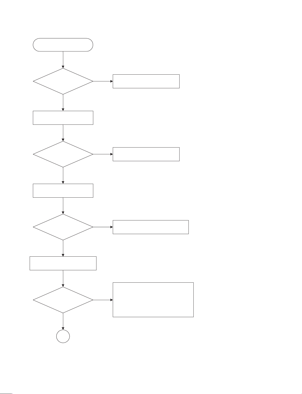
- 2-2 -
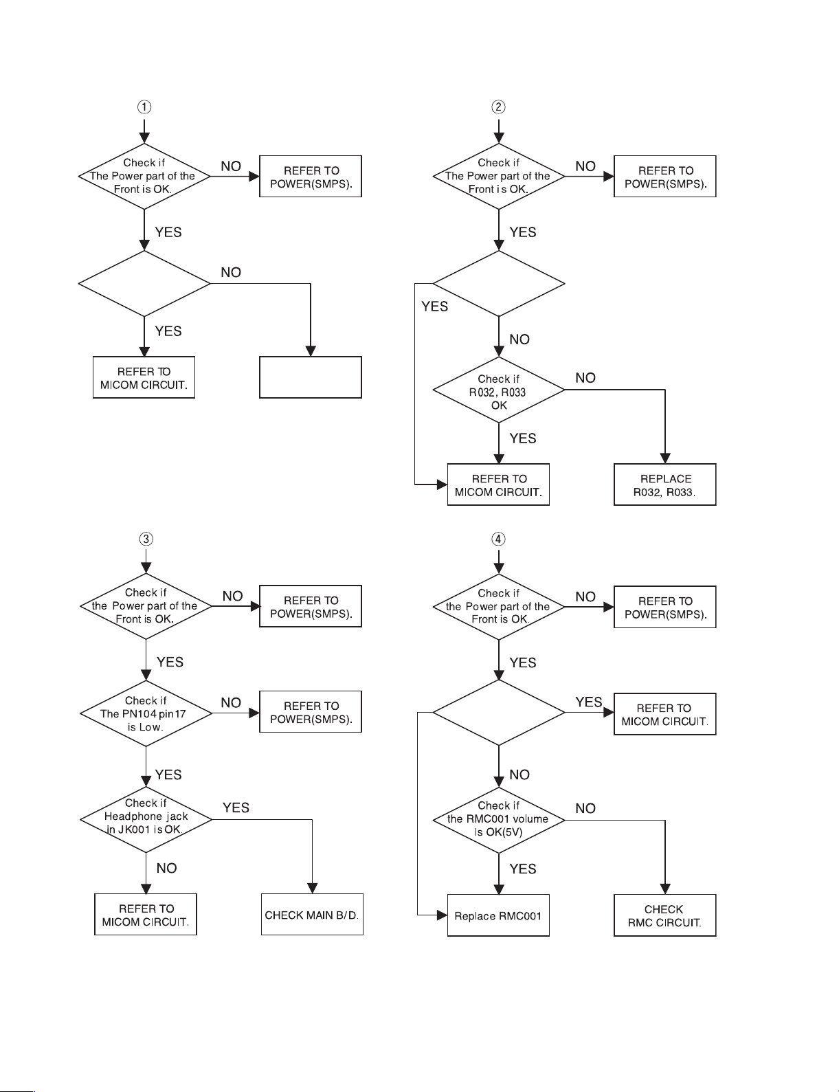
2. AUDIO µ-COM CIRCUIT
POWER ON
Does CD/DVD
appear at FLD?
Does
AV 1/2 FM87.5
appear at FLD?
OK.
Does READING
appear at FLD?
Does no Disc or
Time appear at FLD?
Check if DVD an Audio
Micom Interface is OK.
Check power.
Check DVD Module.
Check SMPS.
Does it appear
DVD Error at
FLD?
Check
Connector(PN902)if
is normally.
Check power part
of Main B/D.
Check oscillator
of x101.
Check if IC101
PIN80 is High.
Reconnect it.
Refer to SMPS
Refer to oscillator
Circuit.
Check DVD Reset Waveform.
Check if IC101
PIN92 is High.
Check if IC101 PIN
31, 32, 51, 88 are high
(5V).
Check if IC101
PIN96 is High.
Replace IC101.
Check IC101 Reset Wavefrom.
Check 5V line.
Check Power section Circuit.
Page 8
- 2-3 -
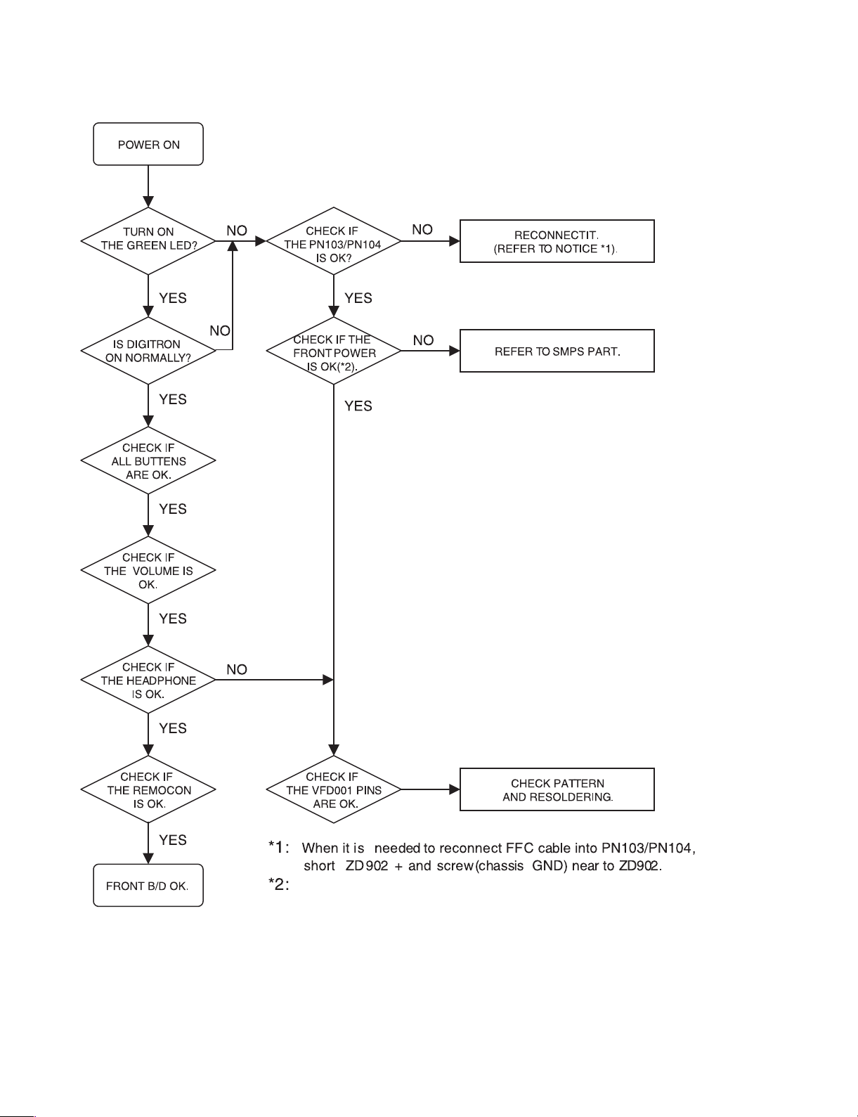
3. FRONT CIRCUIT (1/2)
PIN104 Pins
PIN : -27V
PIN 6 : -18V
PIN7 : -22V
PIN : 5V
Page 9
- 2-4 -
4. FRONT CIRCUIT (2/2)
CHECK
IF R029, R036~R040,
R046~R051
OK.
REPLACE R029,
R036~R040,
R046~R051
Check
if PN104 pins10, 11
Waveform OK.
Check
if the Remocon
Waveform of the
PN104 pin16
Page 10
- 2-5 -
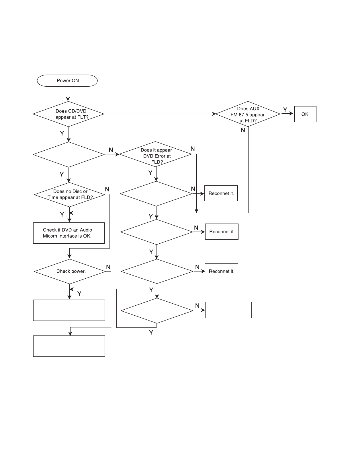
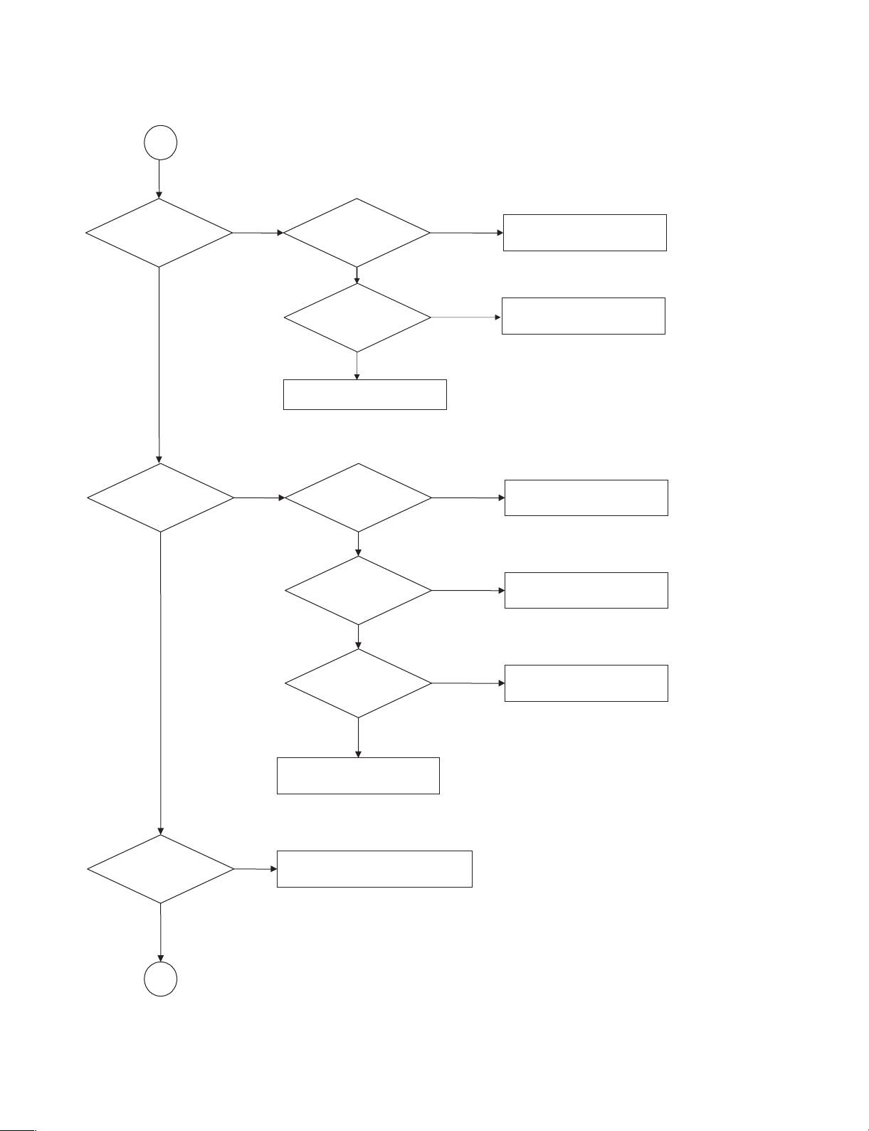
1. POWER CHECK FLOW
DVD TROUBLESHOOTING GUIDE
READING appear at FLD?
Does
Check DVD SECTION
Check
Connector(CN201)
if is normally.
Check
Connector CN202
Check
Connector CN203
Check
voltage each pin for PN902
Check SMPS
board regulator
Check Connector PN902
Page 11
- 2-6 -
2. SYSTEM OPERATION FLOW
Power On
1. 8032 initializes SERVO, DSP & RISC registers
2. Write RISC code to SDRAM
3. Reset RISC
Show LOGO
YES
Tray Closed?
NO
Tray Close to Closed position
SLED at Inner
Side ?
NO
SLED Moves to Inner Positi on
1. Judge whether have disc and disc type
2. Jump to related disc reading procedure
Reci eve
OPEN/CLOSE
Key?
YES
YES
NO
1. Execute Pressed Key & IR Key
2. System operation Routine Loop
1. Stop Playback & Open Tray
2. Display tray open message & LOGO
NO
Receive
CLOSE Key?
YES
Page 12
- 2-7 -
3. TEST & DEBUG FLOW
TEST
Check the AC Voltage
Power PCBA(120V)
YES
Switch on the Power PCBA
Is the DC Voltage
outputs OK?
(5V,3.3V, 8V, 12V, -12V, 11.5V)
YES
Make sure the main PCBA don't
short on VCCs and switch it on.
NO
NO
Replace power PCBA or
AC transformer.
Repair or Replace P ower PCBA
Is 3.3V and 1.8V DC
outputs normal on main
PCBA?
YES
Connect to PC RS232 Cable and
update the FLASH memory code.
Update FLASH
successfully?
YES
A
NO
Check the regulators or related diodes.
1. Check 27MHz system clock.
NO
2. Check system reset circuit.
3. Check FLASH R/W enable signal PRD,RWR.
4. Check RS232 SIGNALS.
5. Check FLASH Memory related circuit.
Page 13
- 2-8 -
A
RESET or Power On.
Show LOGO?
NO
Flash Memory operates
properly?
YESYES
SDRAM works properly?
YES
MT1389 VIDEO outputs
properly?
YES
Have TV signal output?
YES
Check AV cable connection
to TV set.
NO
NO
NO
NO
Check connection lines between FLASH
& MT1389 and the FLASH access time
whether is suitable or not.
Check connection lines between
SDRAM & MT1389 and the SDRAM
is damaged.
Check the related circuit of MT1389.
Check the filtering and amp circuit of
TV signal.
Does Tray move
inside when it is not
at closed position?
YES
B
NO NO
Normal TROUT &
TRIN signals?
YES
Normal TRCLOSE &
TROPEN signal?
YES
Normal LOAD+ &
LOADsignal?
YES
Check the cable connection
between main PCBA and loader.
NO
NO
Check the load OPEN & CLOSE
switch
Check the Tray control IO pins on
MT1389 & IP4504.
Check the Tray control amplifying
circuit on Motor driver.
Page 14
- 2-9 -
B
Does
the SLED move
to inner side when it is at
outter position?
YES YES
NO NO
Motor Driver STBY
Pin is High?
Check the connection line of
STBY signal.
Do not put in disc and tray
close.
Optical Lens has
movements for searching
Focus?
Is FMSO DC Level higher
than 1.4V?
YES
SL+ and SL- output
properly?
YES
Check the cable connection with
NO NO
MECHA.
Proper FOSO outputs
to motor driver?
NO
NO
Check the related circuit of
FMSO.
Check the amp circuit on motor
driver.
Check FOSO connection on
MT1389 and motor dirver.
YESYES
Proper F+ & F- outputs?
YES
C
Check cable connect on with
pick-up head.
NO
Check the amp circuit on motor
dirver.
Page 15
- 2-10 -
C
Laser turns on when
reading disc?
YES
Put disc in? Laser off
YES
Disc ID is correct?
NO
NO
NO
LD01 or LD02 output
properly?
Collector voltage of
power transistor is OK?
Check cable connection between
transistor ouput and pick-up
head.
Proper RFL signal
on MT1389?
YES
YES
YES
NO
NO
NO
Check the laser power circuit
on MT1336 and connecting to
power transistor.
Check the related circuit on
laser power transistor
Check the related circuit
on MT1389 RFL signal.
YES
Does spindle rotate?
YES
D
NO
Check LDO1 & LDO2 signal
Proper DMSO signal on
MT1389
YES
SP+ & SP- output
properly?
YES
Check the cable connection
between spindle and main PCBA.
NO
NO
Check DMSO related
circuit on MT1389.
Check the spindle control
amp circuit of motor
driver.
Page 16
- 2-11 -
D
YES
Focus ON OK?
YES
Track On OK?
YES
NO NO
NO
Proper signals on
A,B,C,D of MT1389
YES
Check FEO signal
on MT1389
YES
Check FOSO signal on MT1389
Normal TEO Signal on
MT1389?
YES
Properly TRSO signal
on MT1389?
YES
NO
NO
NO
Check connections between
MT1389 and pick-up head.
Check the FOSO connection on
MT1389 and motor driver.
Check the related
circuit on MT1389
Check the TRSO
connection on MT1389
and motor dirver.
Disc is play ?
YES
E
NO
T+ & T- output
properly?
YES
Check cable connection on
pick-up head.
Check RFO & RFLVL signal waveform.
NO
Check the tracking control
amp circuit on motor
driver.
Page 17
- 2-12 -
E
Normal Audio output
when disc playback?
YES
Normal IR.VFD & Front
pannel key functions?
YES
TEST END
NO NO
NO
Audio PWM IC received
correct data stream?
YES
Normal Audio PWM IC
out?
YES
Check Audio filter,amplify,mute
IR.VFD Front pannelkey & MT1389
Check the cable connection on
circuit.
Communications between
is normally?
YES
Front pannel.
NO
NO
Check connection between MT1379
& Audio PWM IC.
Check the related
circuit of Audio PWM IC.
Check communication lines on
MT1389.
Page 18
- 2-13 -
DVD DETAILS AND WAVEFORMS ON SYSTEM
TEST AND DEBUGGING
1. SYSTEM 27MHz CLOCK,RESET,FLASH R/W SIGNAL
1) MT1389 main clock is at 27MHz(X601)
2) MT1389 reset is high active
FIG 1-1
FIG 1-2
Page 19
- 2-14 -
3) RS232 waveform during procedure(Downloading)
4) Flash R/W enable signal during download(Downloading)
FIG 1-3
FIG 1-4
Page 20

- 2-15 -
2. SDRAM CLOCK
1) MT1389 main clock is at 27MHz(X601)
3. TRAY OPEN/CLOSE SIGNAL
FIG 2-1
FIG 3-1
Page 21

- 2-16 -
4. SLED CONTROL RELATED SIGNAL
(NO DISC CONDITION)
5. LENS CONTROL RELATED SIGNAL(NO DISC CONDITION)
FIG 4-1
FIG 5-1
Page 22

- 2-17 -
6. LASER POWER CONTROL RELATED SIGNAL
(NO DISC CONDITION)
7. DISC TYPE JUDGEMENT WAVEFORM
FIG 6-1
FIG 7-1
Page 23

- 2-18 -
FIG 7-2 (DVD)
FIG 7-3 (CD)
Page 24

- 2-19 -
8. FOCUS ON WAVEFORM
FIG 7-4 (CD)
FIG 8-1 (DVD)
Page 25

- 2-20 -
FIG 8-2 (CD)
9. SPINDLE CONTROL WAVEFORM (NO DISC CONDITION)
FIG 9-1
Page 26

- 2-21 -
10. TRACKING CONTROL RELATED SIGNAL
(System checking)
FIG 10-1 (DVD)
FIG 10-2 (CD)
Page 27

- 2-22 -
11. MT1389 AUDIO OPTICAL AND COAXIAL INPUT
(SPDIF)
12. MT1389 VIDEO OUTPUT WAVEFORM
1)100%
FIG 11-1 (DVD)
FIG 12-1
Page 28

- 2-23 -
2) COMPOSITE VIDEO SIGNAL
13. MT1389 AUDIO OUTPUT TO PWM IC
FIG 12-2
ADAT0~3
FIG 13-1
Page 29

- 2-24 -
14. AUDIO OUTPUT FROM PWM IC
FIG 14-1
Page 30

- 2-25 -
WIRING DIAGRAM
Page 31

- 2-26 -
BLOCK DIAGRAMS
1. OVERALL BLOCK DIAGRAM
5V
MEMORY SLOT
IC603
M12L64164A
SD33
JK601
HDMI OUT
CONNECTO
3.3V-D1
HDMI PCB ASSY
3.3V-D1,1.8V-D1
ASSY
(7 IN 2)
12MHz
USB_M, USB_P
DCS#, DRAS#, DCAS#,
BA[0:1], SDCLK, SDCKE
64Mb, SDRAM
DDC CLK,DATA
+5V
R
HOT PLUG DET
DATA0~2/+-
IC602
64Mb, SDRAM
HY57V643220CT
13.5MHz
X601
DQ0~31
DAD0~10
IC601
FLI2301
RESOLUTION UP
UP
PICK
M
MOTOR
SPINDLE
A29LV800TA-70
DV33
1M, 8BIT FLASH
DWE#
DQ[00:15]
DQM[0:1]
MA[00:11]
HDMI
IC603
SIL9190
3.3v-D1, 3.3V-M
IC605
MM1234
SWITCHING IC
AV33, DV33
Y,Pb,Pr
FDATA0~7
M_VSYNC, M_HSYNC
LOADING
SLED
(Resolution up)
LOAD+, LOAD-
M
MOTOR
M
MOTOR
IC602
A[00:21]
SPDIF
TX0+,TX0-, TX1+,TX1-,
TX2+,TX2-, TXC+,TXC-,
F+, F-, T+, T-
SP+, SP-
SL+, SL-
AD[0:7]
AV33, DV33
IC606
KS24C021CS
2Kb,
EEPROM
DV33
CN601
RS-232
TXD
PCE#, PRD#, PWR#
IC601
AMCLK
SCL,SDA
LIMIT
SCL
RXD
X601
27MHz
MT1389FE
MPEG & DSP
CD : RFO, A, B, C, D, E, F
DVD : RFO, A, B, C, D
Y,Pb,Pr(Analog)
Y,Pb,Pr(Analog or Digital)
SDA
ALRCK, ABCK
REG_ 12V
IC303
V1P4
TROUT, TRIN, ADIN
V2.0, MDI1
AVCC, APC
LD01, LD02, IOA,
TUNER_L, R
TROPEN, TRCLOSE, TRSO, FOSO, DMSO, FMSO, STBY
DVD_DATAOUT
DVD_CE, DVD_CLK, DATAIN
ADATA
AMCLK
BU4052
X101
12.5MHz
DVD_RESET
AUDIO S/W
JK002
JK003
JK004
AV2_AUDIO L, R_VIDEO
AV2_L, R
4052_SW1,SW2
REG_5VA
IC101
JK503
OPT.
TMP88CU77F
SPDIF
AUDIO MICOM
REG_5VA
FRONT
REAR
RIN, LIN
C/SW
ALRCK, ABCK
DN_MIX
IC305
IC304,
OPAMP
V_MUTE1
V_MUTE2
COMPONET-OUT
COAXIAL IN
IC302
CS42516
CODEC & DIR
AV1_L, R
PS9829_DATA
JK501
AV1-IN
COAXIAL IN
AV1 AUDIO_L, R_VIDEO
PS9829_CLK, RESET, PDN
510_PDN
510_FAULT, TH_WAR
Y, Pb, Pr
MONITOR OUT
AV1_VIDEO
AV2_VIDEO
REG_3.3VA
SL+/
JK502
S-VIDEO
MM1623XFBE
VIDEO 6dB AMP
C+/
FL+/
REG_3.3VA, 34.5VA
L703
L.P.F
Y_OUT, C_OUT
IC605
IC301
PS9829
L702
IC502
V_MUTE1
X301
MODULAT
8CH. PWM
STA510
IC701, IC702
IC703, IC704
L708
S/W
VIDEO
NJM2244
CVBS
V_MUTE2
12.288MHz
OR
FR+/
SW+/
LL705
LL706
JK001
H/PHONE
HEAD PHONE L, R
IC501
H/PHONE+/
SR+/
OPAMP
L710,L711,L712
P_DI
MUTE
IC201
IP4504A
MOTOR DRIVER
RVCC2, +P8V
TUN101
OPTION
RDS_CLK, DATA
P_CE, P_CLK, P_DO
RADIO TUNER MODULE
REG-9V
C
F.L
R.L
SW
JK701
F.R
R.R
SPEAK ER TERMINAL
Page 32

- 2-27 -
2. SMPS BLOCK DIAGRAM
NOTES) Warning
NOTES) Parts that are shaded are critical
NOTES) With respect to risk of fire or
NOTES) electricial shock.
TO I/O
5.3VA
(PSV01)
RECTIFIER &
SMOOTING BLOCK
(D927,C931,L925,C932)
C925)
RECTIFIER &
(D921,C921,L921
SMOOTING BLOCK
T901
!
!
SNUBBER
3.8VA
13VA
GND
GND
(IC956,R950,C953)
(IC953,R947,C928)
12V REG & S/W Block
12VT REG & S/W Block
RECTIFIER &
SMOOTING BLOCK
(D922,C922,L922,C926)
BLOCK
(D901,C905,R901)
GND
33VA
33V S/W Block
(Q923,R943,R934)
RECTIFIER &
SMOOTING BLOCK
54
DRIVE & S/W BLOCK
FL-
FL+
-29VA
R945,C920)
5.0VD S/W Block
5.0VT S/W Block
(Q920,R942,R944
(Q924,R940,R935,R936
FEED-BACK
(D925,C929,)
RECTIFIER &
(D923,C923,L923)
SMOOTING BLOCK
7
C909,C910,R906,
(IC901, D902, D903,
!
2
ZD901,ZD902)
D934,C934)
BLOCK
PHOTO COUPLER
TIMER ‘H’ Block
(R930,R931,
(PC910)
PWR CTL Block
(Q926,R964,R965)
(Q925,R956,R957)
R926,R927,
R928,C930)
(IC941)
ERROR AMP
T902
!
RESET
BLOCK
GND
P-con
35.5V
TO AMP
(PSW01)
(L951,C953,C954)
REGULATION BLOCK
RECTIFIER &
SMOOTING BLOCK
1
(D905,D906)
DRIVE & S/W BLOCK
P-sen
(R951,R952)
RECTIFIER &
(D91,C951,C952)
SMOOTING BLOCK
5
4
C919,ZD912)
(IC902,R919,
C916, C917,C918,
BLOCK
R949,R950,
(R946,R947,
FEED-BACK
(PC912)
PHOTO COUPLER
!
R955,C943)
(IC942)
ERROR AMP
TH901
BD901
+
C903,C904
1
!
3
8
BLOCK
(CM901,L902,
NOISE FILTER
3
2
Y-CAP
C900
!
!
Y-CAP
C901,C902
!
FUSE
L901, CM902)
(F901)
BR BL
(BK)(WH)
Page 33

- 2-28 -
3. SERVO Block Diagram
EEP
ROM
SCL, SDA
PRD#, PWR#
PCE#
MT1389
DVDPLAYER
X601
27MHz
X-TAL
AD[0:7]
ROM
FLASH
A[0:20]
IC601
ONE CHIP
RS232C(MTK)
RXD, TXD
MA[0:11]
DQM0 ,DQM1
WE#,CAS#,RAS#
CS#,BA0,BA1
SDCLK
SDCKE
IC603
SDRAM
DQ[0:15]
4M x 16bit
ALPC
LD0 1, LDO 2, IOA
MDI 1
TRCLOSE
ADIN
IC201
IP4504
STBY,V1P4
FOSO,TRSO,FMSO
DMSO,,TROPEN
Motor Driver
V20, PICKSEL
DVD: A,B,C,D, RFO
CD: A,B,C,D, E, F,RFO
LIMIT,TRIN,TROUT
F+, F-, T+, T-
SL+, SL-
SP+, SP-
LOAD+, LOAD-
UP
PICK
M/D
Page 34

- 2-29 -
4. MPEG & MEMORY Block Diagram
VIDEO
Interface
IC606
EEPROM
Y2(Y),Y3(Color)
Y4(Y),Y5(Cb),Y6(Cr)
ASPECT(16:9)
SCL,SDA
ACLK,ALRCK,ABCK
MUTE,VSCK,VSDA
e
AUDIO
Interfac
ASPDIF
ASTB,SCL,SDA
ASDTA[0:3]
AD[0:7]
A[0:20]
IC602
PWR,PCE,PRD
(16 M )
IC603
SDRAM
64M
FLASH MEMORY
CS,DCKE,MA[0:10]
DCLK,WE,CAS,RAS
DQ[0:15]
DQM0,DQM1
M_REQ
VFD_TXD
VFD_SCK
MT1389
SCKO,TXDO,M-REQ
IC601 (MPEG + DSP + RF)
X601
27MHz
VFD_RXD
URST,S_REQ
AUDIO MICOM
Page 35

- 2-30 -
5. VIDEO & AUDIO Block Diagram
M
A/V
JACK
CVBS
HDMI BOARD
COMPONENT(Y.Pb.Pr)
Amp
IC605
VIDEO 6dB
REAR R
FRONT R
SUPER VIDEO (Y/C)
IC701 Digital
POWER IC
REAR L
FRONT L
IC702 Digital
POWER IC
CENTER
WOOFER
IC303, IC704
Digital POWER IC
5.1CH BOARD
IC301
IC
PWM
(5.1CH)
MODULATOR
FDATA
[0:7]
(Y/C)
(Y.Pb.Pr)
MPEG
ACLK
LRCK
PEG
ADATA2
ADATA1
ADATA3
Page 36

Page 37

- 3-5 -
• PACKING ACCESSORY SECTION
811
PLUG ASS'Y 1WAY(YELLOW)
826
FILTER(CIRC)
808
BATTERY
900
REMOCON
SHEET
804
812
PLUG ASS'Y 2WAY
824
ANTENNA LOOP(AM)
825
ANTENNA (FM)
OWNER'S MANUAL
801
PACKING, CASING
803A
PACKING, CASING
803B
803C
PACKING, CASING
PACKING, CASING
803
802
BOX
Page 38

- 4-1 -
SECTION 4. SPEAKER PART
1. WOOFER SPEAKER SECTION
• MODEL: LHS-75SGW
950
952
A900
954
953
959
955
951
957
958
Page 39

- 4-2 -
2. SPEAKER CENTER SECTION
• MODEL: LHS-75SGC
A700
755
758
754
750
751
753
756
759
756
Page 40

- 4-3 -
3. SPEAKER REAR/FRONT SECTION
• MODEL: LHS-75SGS
A800
859
855
850
851
853
857
854
856
858
Page 41

Page 42

2-31 2-32
AUDIO PART SCHEMATIC DIAGRAMS
• SMPS-1 SCHEMATIC DIAGRAM
A B C D E F G H I J K L M N O P Q R ST
NOTES) Warning
NOTES) Parts that are shaded are critical
NOTES) With respect to risk of fire or
NOTES) electricial shock.
Page 43

• SMPS-2 SCHEMATIC DIAGRAM
A B C D E F G H I J K L M N O P Q R ST
2-33 2-34
Page 44

2-35 2-36
• MICOM SCHEMATIC DIAGRAM
A B C D E F G H I J K L M N O P Q R ST
Page 45

2-37 2-38
• I/O SCHEMATIC DIAGRAM
A B C D E F G H I J K L M N O P Q R ST
Page 46

2-39 2-40
• AMP SCHEMATIC DIAGRAM
A B C D E F G H I J K L M N O P Q R ST
Page 47

2-41 2-42
• FRONT SCHEMATIC DIAGRAM
A B C D E F G H I J K L M N O P Q R ST
Page 48

2-43 2-44
• H/PHONE SCHEMATIC DIAGRAM
A B C D E F G H I J K L M N O P Q R ST
Page 49

2-45 2-46
• AV2 SCHEMATIC DIAGRAM
A B C D E F G H I J K L M N O P Q R ST
Page 50

2-47 2-48
DVD PART SCHEMATIC DIAGRAMS
• MPEG SCHEMATIC DIAGRAM
A B C D E F G H I J K L M N O P Q R ST
Page 51

2-49 2-50
• DSP SCHEMATIC DIAGRAM
A B C D E F G H I J K L M N O P Q R ST
Page 52

2-51 2-52
• SERVO SCHEMATIC DIAGRAM
A B C D E F G H I J K L M N O P Q R ST
Page 53

3-53 3-54
PRINTED CIRCUIT DIAGRAMS
• MAIN P.C. BOARD (TOP SIDE)
Page 54

3-55 3-56
• MAIN P.C. BOARD (BOTTOM SIDE)
Page 55

2-57 2-58
• FRONT P.C.BOARD (TOP SIDE)
• FRONT P.C.BOARD (BOTTOM SIDE)
Page 56

2-59 2-60
• H/PHONE P.C.BOARD (TOP SIDE)
• H/PHONE P.C.BOARD (BOTTOM SIDE)
• AV JACK P.C.BOARD (TOP SIDE)
• AV JACK P.C.BOARD (BOTTOM SIDE)
Page 57

2-61 2-62
• POWER P.C.BOARD
LOCATION GUIDE
NOTES) Warning
NOTES) Parts that are shaded are critical
NOTES) With respect to risk of fire or
NOTES) electricial shock.
Page 58

2-63 2-64
29 1.63
30 1.63
31 1.63
32 1.63
33 26.36
34 26.36
35 31.42
36 31.42
12).IC703(STA510)
10
217.7
317.7
434.5
50
60
734.5
817.7
917.7
10 17.7
11 17.7
12 34.5
13 0
14 0
15 34.5
16 17.7
17 17.7
18 NC
19 0
20 0
21 4.89
22 4.89
23 3.3
24 0
25 3.18
26 3.16
27 3.16
28 3.28
29 1.63
30 1.63
31 1.63
32 1.63
33 26.36
34 26.36
35 31.42
36 31.42
13).IC704(STA510)
10
217.7
317.7
434.5
50
60
734.5
817.7
917.7
11 17.7
12 34.5
13 0
14 0
15 34.5
16 17.7
17 17.7
18 NC
19 0
20 0
21 4.89
22 4.89
23 3.3
24 0
25 3.18
26 3.16
27 3.16
28 3.28
29 1.63
30 1.63
31 1.63
32 1.63
33 26.36
34 26.36
35 31.42
36 31.42
11).IC702(STA510)
10
2 17.7
3 17.7
4 34.5
50
60
7 34.5
8 17.7
9 17.7
10 17.7
11 17.7
12 34.5
13 0
14 0
15 34.5
16 17.7
17 17.7
18 NC
19 0
20 0
21 4.89
22 4.89
23 3.3
24 0
25 3.18
26 3.16
27 3.16
28 3.28
19 0
20 NC
21 NC
22 NC
23 NC
24 4.93
25 0
26 NC
27 NC
28 NC
29 NC
30 NC
31 NC
32 NC
33 NC
34 NC
35 NC
36 NC
37 NC
38 0
39 0
40 0
41 4.94
42 NC
43 NC
44 NC
45 NC
46 NC
47 NC
48 0
49 0
50 NC
51 3.26
52 0
53 3.26
54 0
55 0
56 NC
57 NC
58 NC
59
1.66(12.288MHz)
60 0.32
61 0.32
62 0
63 NC
64 NC
6).IC303(BU4052)
12.75
20
32.75
40
5NC
60
7 -6.25
80
90
10 0
11 0
12 2.75
13 2.75
14 NC
15 0
16 5.95
7).IC304(UTMC4580)
12.84
22.84
32.84
4 -12.31
52.84
62.84
72.84
8 11.68
8).IC305(UTMC4580)
12.86
22.86
32.86
4 -12.32
52.86
62.86
72.86
8 11.69
9).IC501(UTMC4580)
10
20
30
4-11.42
50
60
70
8 11.23
9).IC502(NJM2244M)
12.04
24.82
31.97
44.82
52.82
64.76
72.06
80
10).IC701(STA510)
10
217.7
317.7
434.5
50
60
734.5
817.7
917.7
10 17.7
9 4.95
10 0
11 3.27
12 4.95
13 0
14 0.9
15 0
16 4.91
17 0
18 4.91
19 0
20 4.95
3).IC103(KIA7042)
1 5.1
20
3 5.1
20).IC201(IP4504)
1 1.37
2 2.56
3 2.52
4 2.61
5 2.41
6 2.44
7 2.46
80
9 1.42
10 4.35
11 0
12 0
13 3.94
14 3.94
15 3.19
16 4.7
17 3.9
18 4
19 7.9
20 1.42
21 1.62
22 1.39
23 3.25
24 4.91
25 2.58
26 2.39
27 2.52
28 2.49
4).IC301(PS9829)
10
20
3 2.44
4 4.92
5 3.28
6 2.42
71
80
90
55 -23
56 -23
57 -23
58 -23
59 -23
60 -23
61 -23
62 -23
63 -23
64 -23
65 -23
66 2.5
67 0
68 0
69 4.9
70 4.9
71 0
72 4.8
73 4.8
74 4.8
75 4.4
76 0
77 0
78 0
79 4.8
80 3.9
81 0
82 0
83 0
84 4.8
85 4.8
86 4.8
87 -26
88 4.9
89 1.8
90 0
91 1.8
92 4.8
93 4.35
94 0
95 0
96 5.1
97 4.9
98 0.3
99 0.3
100 0
2).IC102(74HCT244)
10
2 2.48
30
4 2.47
50
6 1.5
70
8 3.27
Volt (V)
MODE
PIN NO.
IC101
(AUDIO MICOM)
10
21.04
34.75
40
50
60
7 4.9
8 4.9
9 4.9
10 4.9
11 2.4
12 4.9
13 0
14 0
15 0
16 0.6
17 5.1
18 0
19 0
20 0
21 0
22 4.9
23 4.9
24 5.1
25 0
26 0
27 5.1
28 0
29 0
30 0
31 5.1
32 4.9
33 -23.4
34 -23.4
35 -23.4
36 -23.4
37 -23.4
38 -23.4
39 -23.4
40 -23.4
41 -23.4
42 -23.4
43 -23.4
44 -23.4
45 -23.4
46 -23.4
47 -23.4
48 -23.4
49 -23.4
50 -23
51 4.88
52 -23.7
53 -23
54 -23
Volt (V)
MODE
PIN NO.
IC102
(74HCT244)
Volt (V)
MODE
PIN NO.
IC103
(KIA7042)
IC201
(IP4504)
IC301
(PS9829)
Volt (V)
MODE
PIN NO.
10 3.28
11 0
12 0
13 2.44
14 0
15 0
16 0
17 0
18 0
19 1.63
20 1.63
21 0
22 3.28
23 1.23
24 1.23
25 1.23
26 1.23
27 NC
28 0
29 3.28
30 NC
31 NC
32 NC
33 NC
34 2.44
35 0
36 NC
37 NC
38 0
39 3.28
40 1.63
41 1.63
42 2.44
43 0
44 0
45 1.63
46 1.63
47 3.28
48 1.63
49 1.63
50 0
51 1.63
52 1.63
53 0
54 1.63
55 1.63
56 3.28
57 0
58 1.63
59 1.63
60 0
61 1.63
62 1.63
63 0
64 0
Volt (V)
MODE
PIN NO.
IC302
(CS42516)
65 3.28
66 2.44
67 1.63
68 1.63
69 0
70 1.63
71 1.63
72 3.28
73 0
74 1.63
75 1.63
76 3.28
77 0
78 0.5
79 0.5
80 2.44
81 0
82 3.28
83 3.28
84 0
85 0
86
1.65(12.288MHz)
87 3.28
88 NC
89 NC
90 NC
91 2.44
92 0
93 NC
94 3.28
95 0
96 4.92
97 NC
98 NC
99 NC
100 NC
1NC
2NC
3NC
43.27
50
64.93
70.65
80
9 0.2
10 0.11
11 0
12 4.93
13 2.83
14 2.83
15 2.83
16 2.83
17 2.75
18 0
Volt (V)
MODE
PIN NO.
IC303
(BU4052)
Volt (V)
MODE
PIN NO.
IC304
(UTMC4580)
IC305
(UTMC4580)
IC501
(UTMC4580)
IC502
(NJM2244M)
IC701
(STA510)
Volt (V)
MODE
PIN NO.
IC702
(STA510)
Volt (V)
MODE
PIN NO.
IC703
(STA510)
IC704
(STA510)
Volt (V)
MODE
PIN NO.
IC601
(MT1389)
10 17.7
11 17.7
12 34.5
13 0
14 0
15 34.5
16 17.7
17 17.7
18 NC
19 0
20 0
21 4.89
22 4.89
23 3.3
24 0
25 3.18
26 3.16
27 3.16
28 3.28
29 1.63
30 1.63
31 1.63
32 1.63
33 26.36
34 26.36
35 31.42
36 31.42
10
2 1.67
3 1.67
4 1.67
5 1.67
6 1.67
7 1.67
8 1.99
92
10 2
11 2
12 1
13 1
14 1
15 1
16 1
17 1
18 2
19 2
20 0.18
21
22 2.34
23 3.21
24 3.2
25 1.55
26 1.93
27 0
Volt (V)
MODE
PIN NO.
28 2.71
29 2
30 1.37
31 1.32
32 1.33
33 1.33
34 2.8
35 2.78
36 2.34
37 2.04
38 1.33
39 0
40 1.37
41 1.37
42 1.4
43 0
44 1.57
45 1.57
46 3.28
47 2.84
48 3.28
49 0
50 3.24
51 0
52 2
53 2.12
54 1.89
55 1.76
56 1.45
57 1.72
58 2.23
59 1.5
60 0.02
61 0
62 0
63 1.7
64 0
65 3.1
66 3.27
67 0.27
68 0.62
69 0.65
70 3
71 1.3
72 1.8
73 3.27
74 1.71
75 2.51
76 0
77 0
78 2.08
79 0
80 3.27
81 1.53
82 1.52
Volt (V)
MODE
PIN NO.
83 1.23
84 0.96
85 0
86 1.3
87 1.68
88 1.32
89 0
90 1.17
91 1.34
92 0.31
93 1.88
94 0
95 1.8
96 3.22
97 1.8
98 2.51
99 2.51
100 3.25
101 3.25
102 3.27
103 3.27
104 2.5
105 1.3
106 2.51
107 3.27
108 3.27
109 0
110 3.9
111 2.52
112 2.6
113 1.93
114 0.02
115 1
116 0
117 1.25
118 1.07
119 0
120 1.82
121 2.35
122 1.8
123 1.14
124 1.13
125 1.27
126 1.33
127 3.27
128 1.3
129 1.4
130 1.3
131 1.2
132 1
133 1
134 0
135 1.2
136 3.28
137 2
Volt (V)
MODE
PIN NO.
138 3.1
139 2.7
140 3.1
141 3.27
142 2.57
143 1.54
144 0
145 1.6
146 0.06
147 0.6
148 0
149 1.95
150 2
151 1.46
152 1.8
153 0.37
154 1.48
155 3.27
156 1.66
157 1.7
158 0
159 0
160 0
161 0
162 1.43
163 0
164 1.45
165 1.59
166 1.43
167 3.27
168 3.27
169 0.77
170 0
171 2.8
172 2.9
173 1.8
174 3.28
175 0
176 3.28
177 3.26
178 0
179 2.89
180 0
181 0.8
182 3.28
183 0.13
184 3.12
185 0.13
186 3.12
187 0.13
188 0
189 3.27
190 1.23
191 1.23
192 2.28
CIRCUIT VOLTAGE CHART
Page 59

2-65 2-66
1 300V
2 GND
3 20V
4 0 ~ 6.5V
5 0 ~ 5V
1 5.6V
25V
3 GND
4 2.5V
1 13V
2 12V
3 GND
4 3.3V
1 4.5V
2 3.3V
3 GND
4 2.5V
1 12V
2 GND
38V
1 2.5V
2 GND
3 4.8V
1 2.5V
2 GND
3 30V
52 0
53 1.1
54 0
17).IC604(LD1117A)
13.27
2 1.8
30
18).IC605(MM1623)
1 4.9
22.33
3 4.9
4 1.1
50
6 1.5
70
82.37
90
10 1.47
11 0
12 2.33
13 4.9
14 2.33
15 0
16 2.39
17 0
18 2.39
19 0
20 1.88
21 1.76
22 0
23 1.74
24 0
25 0
26 0
27 2.38
28 4.9
19).IC606(EEPROM)
10
20
30
40
5 3.2
6 3.2
70
8 3.2
1 GND
2 1 ~ 5V
3 GND
4 0 ~ 6V
5 GND
6 300V
7 12V
8 0 ~ 6V
46 0
47 0
48 0.45
13.27
2 1.2
33.26
41.07
5 1.4
60.12
71.09
81.33
93.27
10 0.96
11 0.7
12 0
13 0.8
14 3.27
15 2
16 3.2
17 2.8
18 3.1
19 2.8
20 2
21 1.72
22 0.06
23 1
24 1.91
25 1.97
26 1.58
27 3.27
28 0
29 1.6
30 1.5
31 1.5
32 1.5
33 0.03
34 0.03
35 0.04
36 NC
37 1.6
38 1.6
39 2
40 NC
41 0
42 1.2
43 3.26
44 1.2
45 0.9
46 0
47 1.5
48 1.5
49 3.26
50 1.3
51 1.3
248 1.9
249 0
250 1
251 1
252 1.6
253 1.53
254 1.5
255 0.9
256 3.2
1 0.4
2 0.8
3 0.8
43
5 2.8
6 0.7
7 0.9
8 1.7
90
10 0
11 3.2
12 3.9
13 3.27
14 3.27
15 1.5
16 0
17 0.3
18 1.9
19 2.5
20 2.3
21 1.4
22 1.9
23 2.2
24 1.95
25 2
26 0
27 0
28 0
29 1.6
30 1.1
31 1.7
32 1
33 1.1
34 0.11
35 1.1
36 0.16
37 3.27
38 1.5
39 1
40 1.5
41 1.2
42 1.3
43 1.2
44 1.4
45 2.09
Volt (V)
MODE
PIN NO.
IC101
(AUDIO MICOM)
193 0
194 0.48
195 3.28
196 0.69
197 0
198 2.9
199 3.27
200 0.5
201 0
202 0.71
203 0.69
204 3.28
205 2.9
206 4.2
207 2.9
208 1.48
209 1.3
210 1.64
211 1.58
212 3.28
213 1.63
214 1.63
215 1.63
216 0
217 1.21
218 1.15
219 1.2
220 0.07
221 1.82
222 1.2
223 0
224 0
225 1.64
226 0
227 1.82
228 0.67
229 0.84
230 1.4
231 1.41
232 0
233 0
234 3.24
235 1.81
236 1.66
237 1.66
238 1.56
239 3.24
240 1.4
241 0
242 1.7
243 1.1
244 3.24
245 1.59
246 1.37
247 1.3
Volt (V)
MODE
PIN NO.
IC602
(FLASH ROM)
Volt (V)
MODE
PIN NO.
IC603
(SDRAM)
IC604
(LD1117A)
IC605
(MM1623)
IC606
(EEPROM)
IC901
Volt (V)
MODE
PIN NO.
Volt (V)
MODE
PIN NO.
IC902
IC902
IC922
IC923
IC924
IC941
IC942
Page 60

3-1 3-2
SECTION 3. EXPLODED VIEWS
• CABINET AND MAIN FRAME SECTION
NOTE) Refer to “SECTION 5 REPLACEMENT
PARTS LIST” in order to look for the
part number of each part.
A43
A50
452
A42
274
A49
283
292
452
463
255
463
A26
252
A60
463
A47
463
A40
463
250
NOTES) Warning
NOTES) Parts that are shaded are critical
NOTES) With respect to risk of fire or
NOTES) electricial shock.
463
279
280
A49A
452
261
261
260
463
253
266
261
A44
463
468
264
300
265
267
A46
463
263
468
Page 61

3-3 3-4
• DECK MECHANISM EXPLODED VIEW
003
004
005
006
038
434
013
012
049
008
010
011
014
054
434
052
055
044
017
045
431
435
046
048
061
019
030
020
431
058
431
021
059
024
050
022
023
026
057
434
043
042
434
056
051
027
025
007
001
436
002
435
016
039
040
041
060
434
009
037
034
047
433
438
432
036
437
032
035
033
062
028
029
015
A26
031
018
434
 Loading...