

Page 1
DVD/CD & KARAOKE RECEIVER
SERVICE MANUAL
MODELS : LH-TK551TB/LH-T551TB
LHS-55TBC, LHS-55TBS,
LHS-55TBW
MODELS : LH-TK551TB/LH-T551TB LHS-55TBC, LHS-55TBS, LHS-55TBWSERVICE MANUAL
Page 2

1-1
[CONTENTS]
SECTION 1.GENERAL
• SERVICING PRECAUTIONS . . . . . . . . . . . . . . . . . . . . . . . . . . . . . . . . . . . . . . . . . . . . . . . 1-2
• ESD PRECAUTIONS . . . . . . . . . . . . . . . . . . . . . . . . . . . . . . . . . . . . . . . . . . . . . . . . . . . . 1-4
• SPECIFICATIONS . . . . . . . . . . . . . . . . . . . . . . . . . . . . . . . . . . . . . . . . . . . . . . . . . . . . . . . .1-5
SECTION 2. AUDIO PART
• AUDIO TROUBLESHOOTING GUIDE . . . . . . . . . . . . . . . . . . . . . . . . . . . . . . . . . . . . . . . . 2-1
• WIRING DIAGRAM . . . . . . . . . . . . . . . . . . . . . . . . . . . . . . . . . . . . . . . . . . . . . . . . . . . . . . . 2-4
• BLOCK DIAGRAM . . . . . . . . . . . . . . . . . . . . . . . . . . . . . . . . . . . . . . . . . . . . . . . . . . . . . . . 2-6
• SCHEMATIC DIAGRAMS . . . . . . . . . . . . . . . . . . . . . . . . . . . . . . . . . . . . . . . . . . . . . . . . . 2-8
• PRINTED CIRCUIT DIARGAMS . . . . . . . . . . . . . . . . . . . . . . . . . . . . . . . . . . . . . . . . . . . . 2-22
SECTION 3.DVD & AMP PART
• ELECTRICAL TROUBLESHOOTING GUIDE . . . . . . . . . . . . . . . . . . . . . . . . . . . . . . . . . . .3-1
• DVD PART SCHEMATIC DIAGRAMS . . . . . . . . . . . . . . . . . . . . . . . . . . . . . . . . . . . . . . . .3-22
SECTION 4. EXPLODED VIEWS . . . . . . . . . . . . . . . . . . . . . . . . . . . . . . . . . . . . .4-1
SECTION 5. SPEAKER PART . . . . . . . . . . . . . . . . . . . . . . . . . . . . . . . . . . . . . . .5-1
SECTION 6. REPLACEMENT PARTS LIST . . . . . . . . . . . . . . . . . . . . . . . . . . . . .6-1
Page 3
1-2
SERVICING PRECAUTIONS
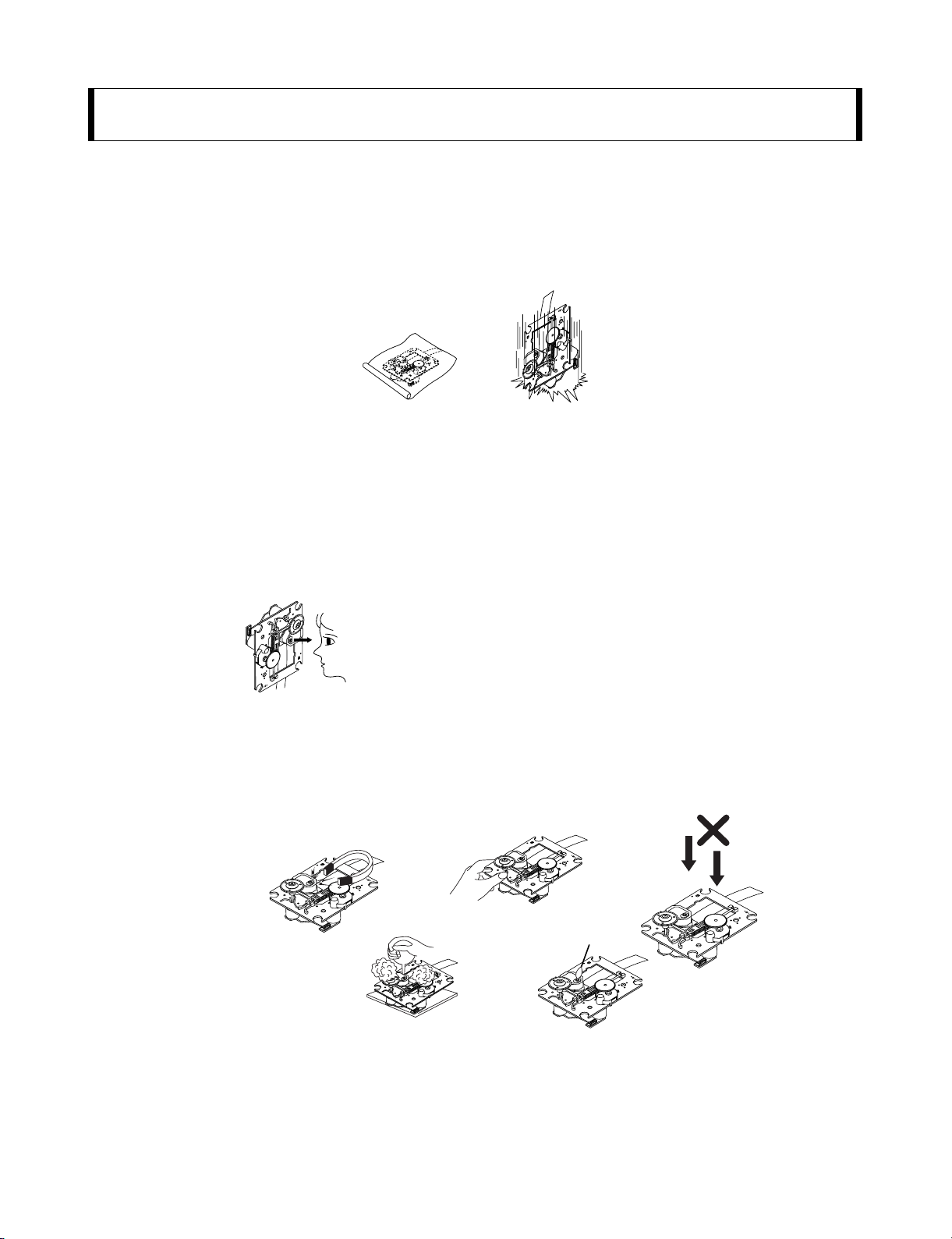
NOTES REGARDING HANDLING OF THE PICK-UP
1. Notes for transport and storage
1) The pick-up should always be left in its conductive bag until immediately prior to use.
2) The pick-up should never be subjected to external pressure or impact.
2. Repair notes
1) The pick-up incorporates a strong magnet, and so should never be brought close to magnetic materials.
2) The pick-up should always be handled correctly and carefully, taking care to avoid external pressure and
impact. If it is subjected to strong pressure or impact, the result may be an operational malfunction and/or
damage to the printed-circuit board.
3) Each and every pick-up is already individually adjusted to a high degree of precision, and for that reason
the adjustment point and installation screws should absolutely never be touched.
4) Laser beams may damage the eyes!
Absolutely never permit laser beams to enter the eyes!
Also NEVER switch ON the power to the laser output part (lens, etc.) of the pick-up if it is damaged.
5) Cleaning the lens surface
If there is dust on the lens surface, the dust should be cleaned away by using an air bush (such as used
for camera lens). The lens is held by a delicate spring. When cleaning the lens surface, therefore, a cotton swab should be used, taking care not to distort this.
6) Never attempt to disassemble the pick-up.
Spring by excess pressure. If the lens is extremely dirty, apply isopropyl alcohol to the cotton swab.
(Do not use any other liquid cleaners, because they will damage the lens.) Take care not to use too much
of this alcohol on the swab, and do not allow the alcohol to get inside the pick-up.
Storage in conductive bag
Drop impact
NEVER look directly at the laser beam, and don’t let
contact fingers or other exposed skin.
Magnet
How to hold the pick-up
Conductive Sheet
Cotton swab
Pressure
Pressure
SECTION 1. GENERAL
Page 4
1-3
NOTES REGARDING COMPACT DISC PLAYER REPAIRS
1. Preparations
1) Compact disc players incorporate a great many ICs as well as the pick-up (laser diode). These components
are sensitive to, and easily affected by, static electricity. If such static electricity is high voltage, components
can be damaged, and for that reason components should be handled with care.
2) The pick-up is composed of many optical components and other high-precision components. Care must be
taken, therefore, to avoid repair or storage where the temperature of humidity is high, where strong magnetism is present, or where there is excessive dust.
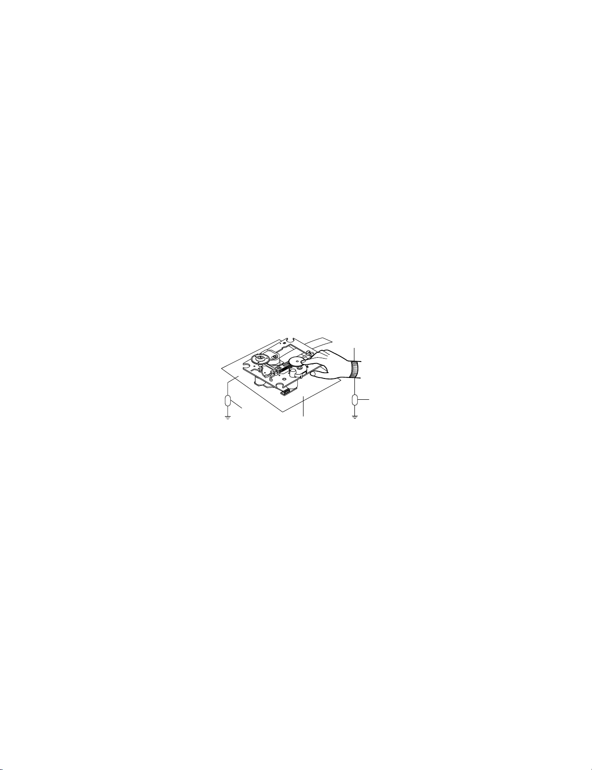
2. Notes for repair
1) Before replacing a component part, first disconnect the power supply lead wire from the unit
2) All equipment, measuring instruments and tools must be grounded.
3) The workbench should be covered with a conductive sheet and grounded.
When removing the laser pick-up from its conductive bag, do not place the pick-up on the bag. (This is
because there is the possibility of damage by static electricity.)
4) To prevent AC leakage, the metal part of the soldering iron should be grounded.
5) Workers should be grounded by an armband (1M Ω)
6) Care should be taken not to permit the laser pick-up to come in contact with clothing, in order to prevent
static electricity changes in the clothing to escape from the armband.
7) The laser beam from the pick-up should NEVER be directly facing the eyes or bare skin.
Resistor
(1 Mohm)
Conductive
Sheet
Resistor
(1 Mohm)
Armband
Page 5
1-4
ESD PRECAUTIONS
Electrostatically Sensitive Devices (ESD)
Some semiconductor (solid state) devices can be damaged easily by static electricity. Such components
commonly are called Electrostatically Sensitive Devices (ESD). Examples of typical ESD devices are integrated
circuits and some field-effect transistors and semiconductor chip components. The following techniques should
be used to help reduce the incidence of component damage caused by static electricity.
1. Immediately before handling any semiconductor component or semiconductor-equipped assembly, drain off
any electrostatic charge on your body by touching a known earth ground. Alternatively, obtain and wear a
commercially available discharging wrist strap device, which should be removed for potential shock reasons
prior to applying power to the unit under test.
2. After removing an electrical assembly equipped with ESD devices, place the assembly on a conductive surface
such as aluminum foil, to prevent electrostatic charge buildup or exposure of the assembly.
3. Use only a grounded-tip soldering iron to solder or unsolder ESD devices.
4. Use only an anti-static solder removal device. Some solder removal devices not classified as "anti-static" can
generate electrical charges sufficient to damage ESD devices.
5. Do not use freon-propelled chemicals. These can generate electrical charges sufficient to damage ESD
devices.
6. Do not remove a replacement ESD device from its protective package until immediately before you are
ready to install it. (Most replacement ESD devices are packaged with leads electrically shorted together by
conductive foam, aluminum foil or comparable conductive materials).
7. Immediately before removing the protective material from the leads of a replacement ESD device, touch the
protective material to the chassis or circuit assembly into which the device will by installed.
CAUTION : BE SURE NO POWER IS APPLIED TO THE CHASSIS OR CIRCUIT, AND OBSERVE ALL OTHER
SAFETY PRECAUTIONS.
8. Minimize bodily motions when handing unpackaged replacement ESD devices. (Otherwise harmless motion
such as the brushing together of your clothes fabric or the lifting of your foot from a carpeted floor can generate static electricity sufficient to damage an ESD device).
CAUTION. GRAPHIC SYMBOLS
THE LIGHTNING FLASH WITH APROWHEAD SYMBOL. WITHIN AN EQUILATERAL TRIANGLE, IS
INTENDED TO ALERT THE SERVICE PERSONNEL TO THE PRESENCE OF UNINSULATED
“DANGEROUS VOLTAGE” THAT MAY BE OF SUFFICIENT MAGNITUDE TO CONSTITUTE A RISK OF
ELECTRIC SHOCK.
THE EXCLAMATION POINT WITHIN AN EQUILATERAL TRIANGLE IS INTENDED TO ALERT THE
SERVICE PERSONNEL TO THE PRESENCE OF IMPORTANT SAFETY INFORMATION IN SERVICE
LITERATURE.
Page 6

1-5
GENERAL
Power supply Refer to main label
Power consumption Refer to main label
Mass 3.9 kg
External dimensions (W x H x D) 430 x 54 x 350 mm
Operating conditions Temperature: 5°C to 35°C, Operation status: Horizontal
Operating humidity 5% to 85%
CD/DVD
Laser Semiconductor laser, wavelength 650 nm
Signal system PAL 625/50, NTSC 525/60
Frequency response (audio) 200 Hz to 20 kHz
Signal-to-noise ratio (audio) More than 75 dB (1 kHz, NOP, 20 kHz LPF/A-Filter)
Dynamic range (audio) More than 70 dB
Harmonic distortion (audio) 0.5 % (1 kHz, at 12W position) (20 kHz LPF/A-Filter)
VIDEO
Video input 1.0 V (p-p), 75 Ω, negative sync., RCA jack x 1/ SCART (TO TV)
Video output 1.0 V (p-p), 75 Ω, negative sync., RCA jack x 1/ SCART (TO TV)
S-video output (Y) 1.0 V (p-p), 75 Ω, negative sync., Mini DIN 4-pin x 1
(C) 0.3 V (p-p), 75 Ω
Component Video output (Y) 1.0 V (p-p), 75 Ω, negative sync., RCA jack x 1
(Pb)/(Pr) 0.7 V (p-p), 75 Ω, RCA jack x 1
TUNER
FM
Tuning Range 87.5 - 108.0 MHz or 65.0 - 74.0 MHz, 87.5 - 108.0 MHz
Intermediate Frequency 10.7 MHz
Signal-to Noise Ratio 60 dB (Mono)
Frequency Response 140 - 10,000 Hz
AM [MW]
Tuning Range 522 - 1,620 kHz or 520 - 1,720 kHz
Intermediate Frequency 450 kHz
AMPLIFIER(LH-TK551TB/LH-T552TB)
Stereo mode 70W + 70W (8Ω at 1 kHz, THD 10 %)
Surround mode Front: 70W + 70W (THD 10 %)
Centre*: 70W
Surround*: 70W + 70W (8Ω at 1 kHz, THD 10 %)
Subwoofer*: 150W (4Ω at 30 Hz, THD 10 %)
SPEAKERS
Satellite Speaker Centre speaker Passive Subwoofer
(LHS-55TBS) (LHS-55TBC) (LHS-55TBW)
Type 1 Way 2 Speaker 1 Way 2 Speaker 1 Way 1 Speaker
Impedance 8 Ω 8 Ω 4 Ω
Frequency Response 150 - 20,000 Hz 150 - 20,000 Hz 40 - 1,500 Hz
Sound Pressure Level 86 dB/W (1m) 86 dB/W (1m) 82 dB/W (1m)
Rated Input Power 70 W 70 W 150 W
Max. Input Power 140 W 140 W 300 W
Net Dimensions
(WxHxD) 280 x 1200 x 280 mm 500 x 83 x 90 mm 195 x 402 x 360 mm
Net Weight 2.38kg 0.71kg 6.2kg
(* Depending on the sound mode
settings and the source, there
may be no sound output.)
SPECIFICATIONS
Page 7
2-1
SECTION 2. AUDIO PART
AUDIO TROUBLESHOOTING GUIDE
1. POWER SUPPLY CIRCUIT
Page 8

2-2
2. FRONT CIRCUIT (1/2)
PIN3
PIN4
PIN9
CN902 CN902
: -32.4 VKK
: -27.5 FL: -23.7 FL+
: +5.0
Page 9
2-3
3. FRONT CIRCUIT (2/2)
Page 10
2-4 2-5
WIRING DIAGRAM
WIRELESS
PN801
CN350
OPTICALINSCART
JACK
MAIN PCB
PDM01 PDM03
23PIN 11PIN 24PIN 23PIN
OPTION
SW
AV1,2
COMPONENT
MONITOR OUT
S-VIDEO OUT
PN103
TUNER
PN104
SPEAKER TERMINAL
30PIN
PN302
AMP PCB
PN105
PN902 PN303
14PIN 14PIN
5PIN
MIC
JACK
MIC
JACK
6PIN
CN001
MIC&USB PCB
USB JACK
MD
PN005
PN002
PN001
SMPS PCB
VFD
FRONT
FRONT
PCB
PCB
H/P JACK
Page 11
2-6 2-7
BLOCK DIAGRAM
Optical
Tuner
AV1
AV2
(option)
Monitor Out
S-AV
Component
Scart
(option)
USB Port
MIC
Wireless
L
R
V
L
R
V
G
B
R
L
R
L
R
G
B
R
8
16
V
MIC1
MIC2
7V
Tuner-L/R
AV1-L/R
AV2-L/R
SCART-L/R
SCART-ID
SCART-FB
(A)(T_CE,T_DO,T_DI,T_CLK,T_RDS_DATA,T_RDS,CLK)
Audio s/w
Bu 4052
CTL-A/B
AV1-CVBS
AV2-CVBS
Monitor out
SCART-CVBS out
C
Y
ALC
BA 3308
MIC1_DET(A)
MIC2_DET(A)
(B)
Slide
S/W
VIDEO-SW
Mixing
+
P
(R) ,Pr(R)
b
(A)
Video S/W
NJM 2279
out
(CVBS-S/W)
DVD-CVBS
Y
Y(G)
USB Controller
CS 5340
ADC
/RST-AD
ADC
CS 5340
Fs = 48kHz
Fx
/RST-AD
SW1, SW2,MUTE1
(A)
Video
S/W
NJM2279
(Y-S/W)
ALRCK,ABCK
MCLK,AMDAT
(A)
SPDI
F
AD-DATA
AD-BCK
AD-LRCK
CS 8406
(slave)
(A)
C
YY
DVD BLOCK
CVB
S
MUTE
TR Mute
(ES 6698)
Mic Volume : OSD CTL
SS
T
12.288MHz
DIT
8406_SDI,8406_SD
O
8406_CLK,8406_CE
(A)
8406_RST,8406_IN
T
SPDIF
OPTION
LRCK
BCK
ADAT 0,1,2,3
(FL/R,RL/R,C/SW
)
AUDIO MICOM
LC876B48
(PIN MAP )
FRONT
PS 9818
(PWM)
(A) HP_DET
STA510A
AMP IC
AM
(A)
FAN1_CTL
FAN2_CTL
PDN
TH_W
FAN1
FAN2
H/P
OPTION
Page 12
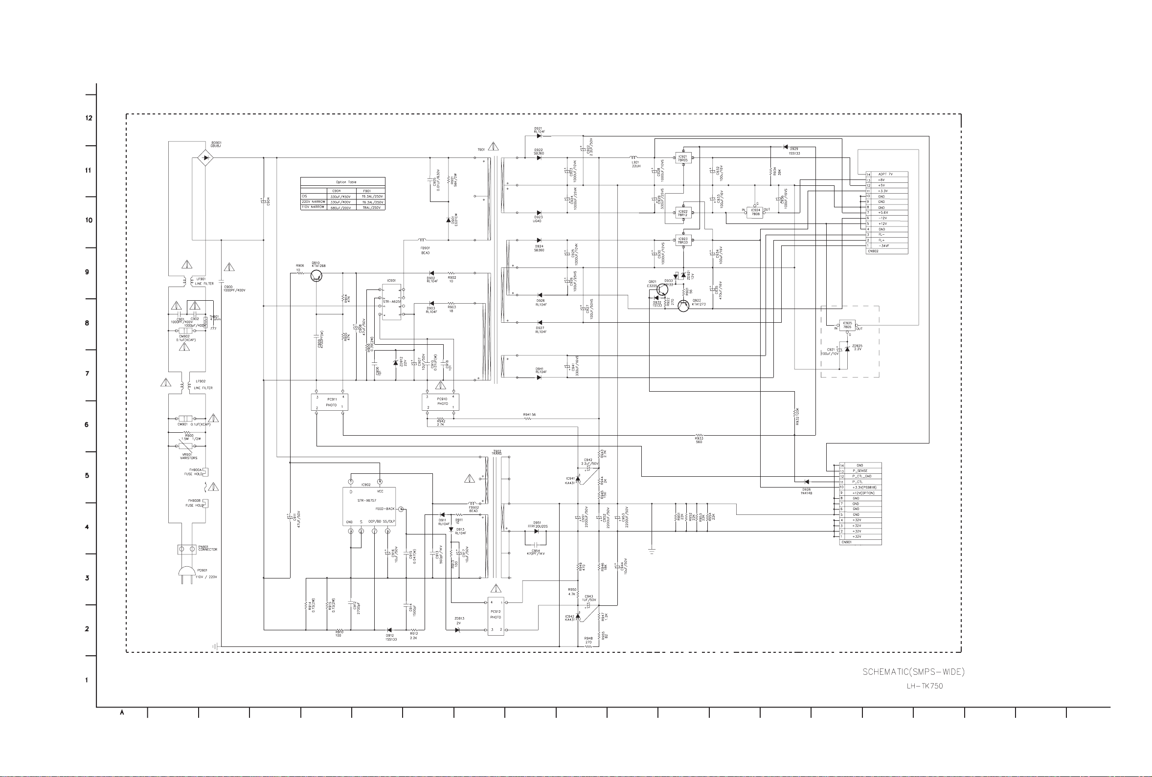
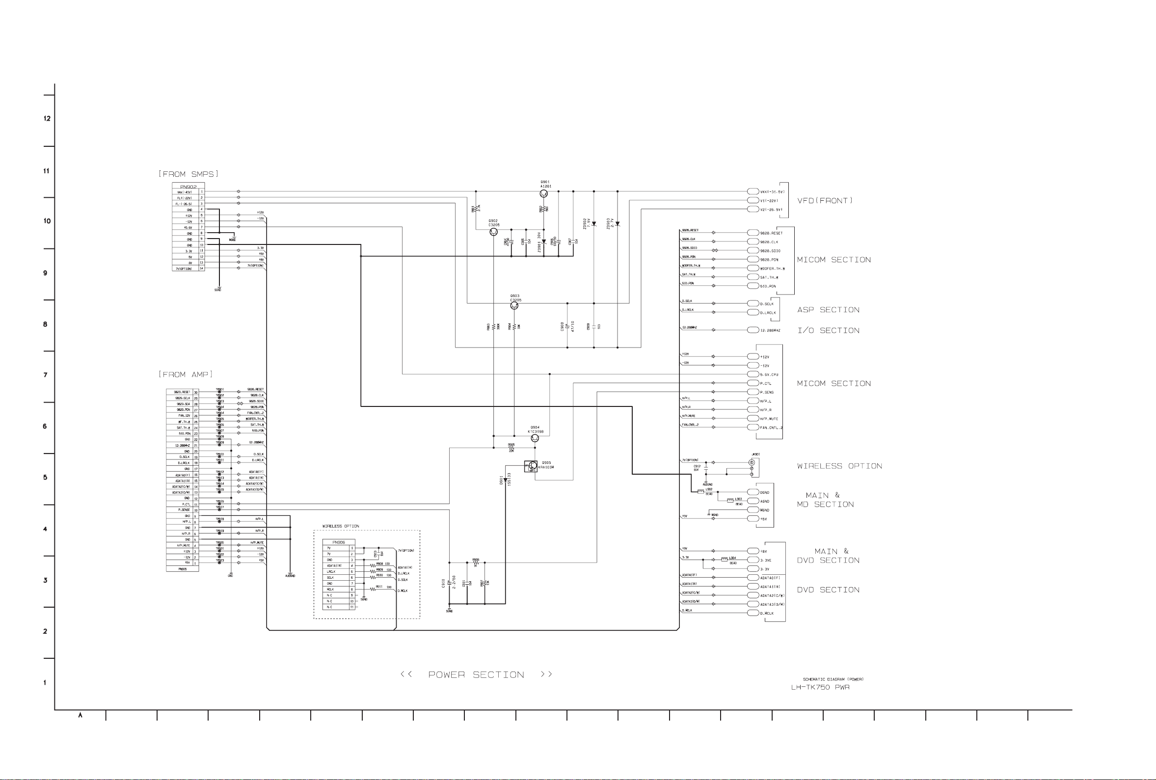
2-8 2-9
SCHEMATIC DIAGRAMS
1. POWER SCHEMATIC DIAGRAM_1
A B C D E F G H I J K L M N O P Q R ST
Page 13
2-10 2-11
2. POWER SCHEMATIC DIAGRAM_2
A B C D E F G H I J K L M N O P Q R ST
Page 14
2-12 2-13
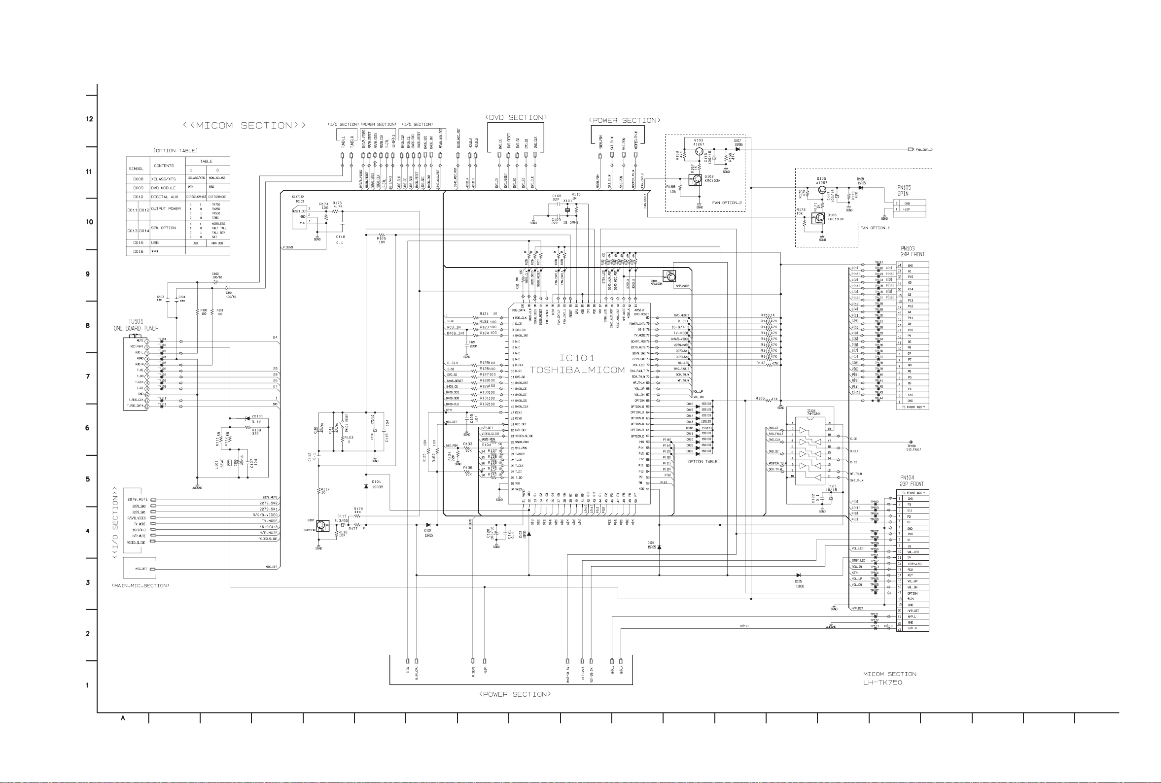
3. MICOM SCHEMATIC DIAGRAM
A B C D E F G H I J K L M N O P Q R ST
Page 15
2-14 2-15
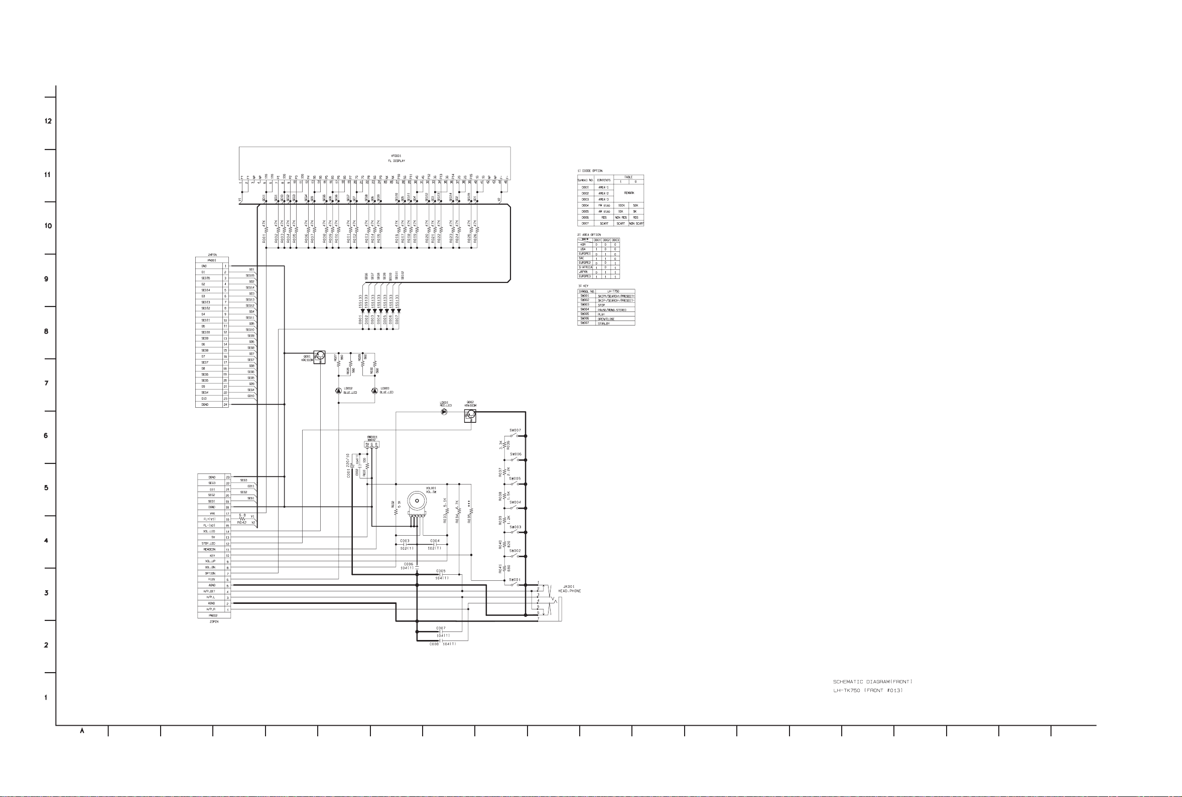
4. FRONT SCHEMATIC DIAGRAM
A B C D E F G H I J K L M N O P Q R ST
Page 16

2-16 2-17
5. DSP& SCHEMATIC DIAGRAM
A B C D E F G H I J K L M N O P Q R ST
Page 17
2-18 2-19
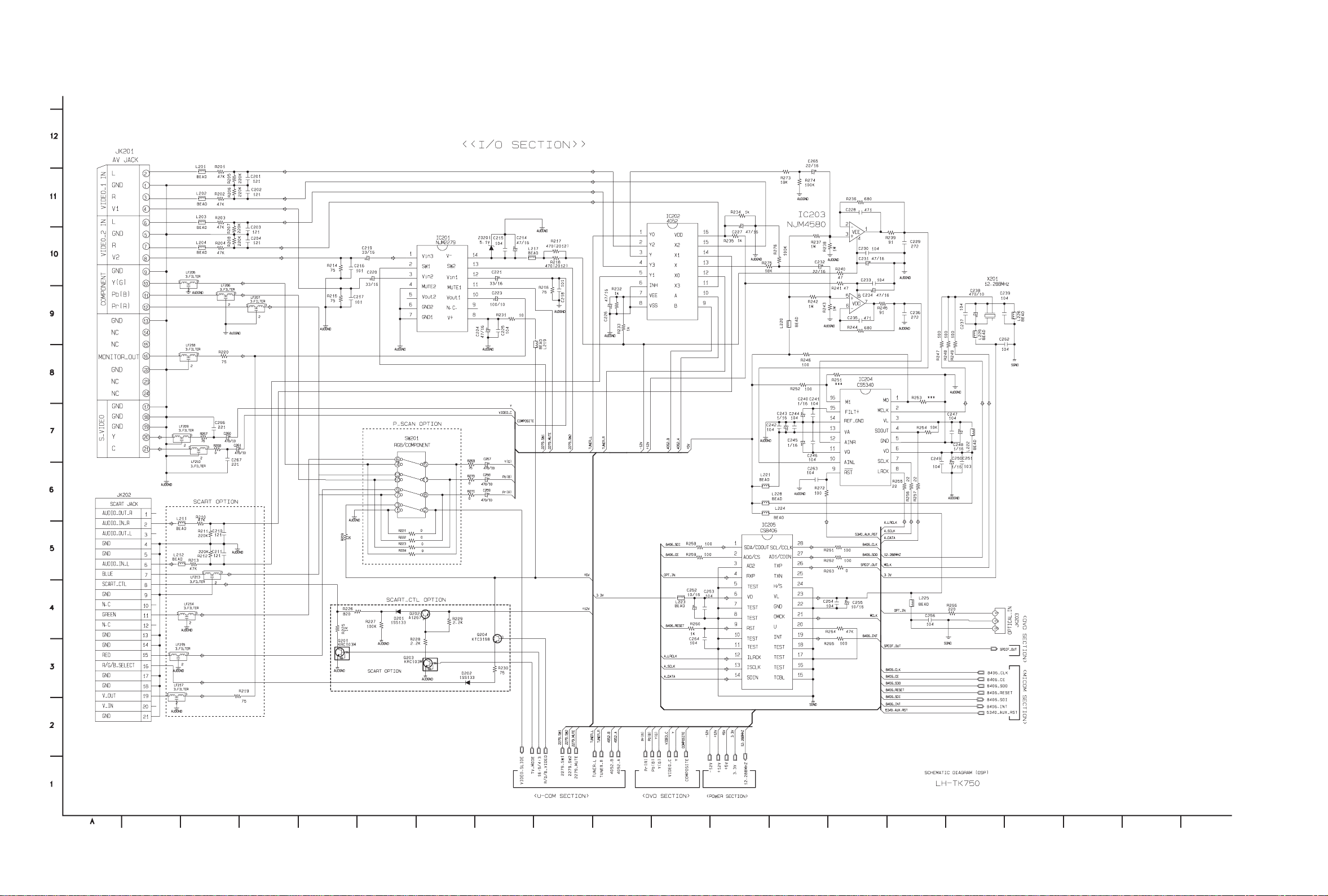
6. I/O SCHEMATIC DIAGRAM
A B C D E F G H I J K L M N O P Q R ST
Page 18

2-20 2-21
7. MAIN MIC SCHEMATIC DIAGRAM
A B C D E F G H I J K L M N O P Q R ST
Page 19

2-22 2-23
PRINTED CIRCUIT BOARD DIAGRAMS
1. MAIN/DVD P.C. BOARD DIAGRAM ( TOP VIEW )
Page 20

2-24 2-25
2. MAIN/DVD P.C. BOARD DIAGRAM ( BOTTOM VIEW )
Page 21

2-26 2-27
3. FRONT MIC P.C. BOARD
Page 22

2-28 2-29
4. SMPS P.C. BOARD
LOCATION GUIDE
5. MIC P.C. BOARD(OPTIONAL PART)
( 5 TOOL )
LOCATION GUIDE
( 7 TOOL )
( TOP VIEW )
( BOTTOM VIEW )
Page 23

2-30 2-31
6. AMP P.C. BOARD
( TOP VIEW )
( BOTTOM VIEW )
( TOP VIEW )
( 5 TOOL ) ( 7 TOOL )
( BOTTOM VIEW )
Page 24

3-1
ELECTRICAL TROUBLESHOOTING GUIDE
1. System operation flow
SECTION 3. DVD & AMP PART
Power On
1. 8082 initializes SERVO, DSP & RISC registers
2. Write RISC code to SDRAM
3. Reset RISC
Show LOGO
Yes
SLED Moves to Inner Position
1. Judge whether have disc and disc type
2. Jump to related disc reading procedure
Tray Closed?
No
Tray Close to Closed position
SLED at Inner
Side?
No
Recieve
OPEN/ CLOSE
Key?
Yes
No
1. Execute Pressed Key & IR Key
2. Systemoperati on Routi ne Loop
1. Stop Playback & Open Tray
2. Display tray open message & LOGO
No
Receive
CLOSE Key?
Yes
Page 25

3-2
2. Test & debug flow
TEST
Check the
AC Vol tage
Power PCBA (110V
or 220V)
Yes
Switch on the Power PCBA
Is the
DC Voltage
outputs OK? (-44V, -22V,
-26.5V, ±12V, 5.6V, 3.3V,
5V, 7V, 8V)
Yes
Is 3.3V and 5V DC
outputs normal on main
PCBA?
Yes
Update
FLASH
successfully?
No
No
No
No
Check the POWER PART
Check the POWER PART
Check the regulators or diode.
1. Check 27MHz system clock.
2. Check systemreset circuit.
3. Check FLASH R/Wenable signal PRD,
RWR.
4. Check FLASH Memory related circuit.
Yes
Replace FLASH
A
Page 26

3-3
A
, 115.
Page 27

3-4
B
Page 28

3-5
C
ES6698.
ES6698.
ES6698.
Page 29

3-6
D
Page 30

3-7
E
PWM IC
received correct data
stream?
Normal
PWM IC out?(IC301)
Check Digital Amp circuit
(IC701, IC702, IC703, IC704)
Check connection between
IC300 ABCK, ALRCK,
ASDAT
Check the related circuit of
PWM.(Check Audio out
Pins52, 54, 55, 59,62, 68
Page 31

3-8
3. AUDIO µ-COM Circuit(DVD & AMP)
YES
Does CD/DVD appear
at FLD?
Does CD/DVD appear
at FLD?
OK
Does Loading appear
at FLD?
POWER ON
YES YES
YES
Does no Dise or Time
appear at FLD?
NO NO
NO
NO
NO
NO
NO
NO
Does it appear DVD Error
at FLD?
Refer to SMPS.
Refer to oscillator Circuit.
Check IC101 Reset
Waveform.
Check 3.3V line.
Check Power section
Circuit.
NO
Check power part of Main
B/D.
Check oscillator of X101.
Check if IC101 Pin80
is high.
Check if IC101 Pin32, 51,
80 are high(5V).
Check if IC101 Pin96
is high.
Replace IC101.
NO
NO
Check if DVD an Audio
Micom Insert is OK.
Check Power.
YES
Check DVD Module.
YES
Check SMPS.
YES YES
YES
YES
YES
YES
YES
Page 32

3-9
DETAILS AND WAVEFORMS ON SYSTEM TEST AND DEBUGGING
1. SYSTEM 27MHz CLOCK,RESET,FLASH R/W SIGNAL
1) ES6698FD main clock is at 27MHz(X501)
3.8V, 27MHz
FIG 1-1
2) ES6698FD reset is high active.
PWR_CTL(SYSTEM µ-COM)
IC501 PIN83)
5.2VA
Power Cord in
M_RESET(IC501 PIN 207)
URST(IC501 PIN 188)
FIG 1-2
Page 33

3-10
2. SDRAM CLOCK
1) ES6698FD main clock is at 27MHz(X501)
(IC503 PIN 38)
DCLK = 93MHz, Vp-p=2.2, Vmax=2.7V
FIG 2-1
4) Flash R/W enable signal during download(Downloading)
FRD(IC500 PIN 28)
FWR(IC500 PIN 11)
FIG 1-4
Page 34

3-11
3. TRAY OPEN/CLOSE SIGNAL
1) Tray open/close waveform
OPEN((PDM03 PIN7)
CLOSE(PDM03 PIN8)
TROPEN(IC402 PIN 4)
TRCLOSE(IC402 PIN 5)
FIG 3-1
2) Tray close waveform
OPEN((PDM03 PIN7)
CLOSE(PDM03 PIN8)
TROPEN(IC402 PIN 4)
TRCLOSE(IC402 PIN 5)
FIG 3-2
Page 35

3-12
4. SLED CONTROL RELATED SIGNAL (NO DISC CONDITION)
FMSO(2.0V/1.4V/1.0V)
(IC501 PIN 19)
STBY(5V) – (IC401 PIN 50)
SL+(4.7V/3.6V/1.9V)
(IC404 PIN 12)
SL-(5.3V/3.7V/2.5V)
(IC404 PIN 11)
FIG 4-1
3) Tray open waveform
OPEN(PDM03 PIN7)
CLOSE(PDM03 PIN8)
TROPEN(IC402 PIN 4)
TRCLOSE(IC402 PIN 5)
FIG 3-3
Page 36

3-13
5. LENS CONTROL RELATED SIGNAL(NO DISC CONDITION)
FOSO(1.5V/1.4V/1.3V)
(IC501 PIN 12)
F+(4.0V/3.6V/3.2V)
(IC404 PIN 14)
F-(4.0V/3.6V/3.2V)
(IC404 PIN 13)
FIG 5-1
6. LASER POWER CONTROL RELATED SIGNAL(NO DISC CONDITION)
MDI1(0V/180mV)
(IC401 PIN 26)
LD01(5.0V//3.5V)
IC401 PIN 20)
LD02(5.0V/3.6V)
(IC401 PIN 21)
FIG 6-1
Page 37

3-14
F+(IC404 PIN 14)
FE(IC401 PIN 40)
RFL(IC401 PIN 19)
FIG 7-2 (DVD)
7. DISC TYPE JUDGEMENT WAVEFORMS
F+(IC404 PIN 14)
FE(IC401 PIN 40)
RFL(IC401 PIN 19)
FIG 7-1 (DVD)
Page 38

3-15
F+(IC404 PIN 14)
FE(IC401 PIN 40)
RFL(IC401 PIN 19)
FIG 7-3 (CD)
F+(IC404 PIN 14)
FE(IC401 PIN 40)
RFL(IC401 PIN 19)
FIG 7-4 (CD)
Page 39

3-16
FE(IC401 PIN 40)
FOSO(IC501 PIN12)
F+(IC404 PIN 14)
F-(IC404 PIN 13)
FIG 8-2 (CD)
8. FOCUS ON WAVEFORMS
FE(IC401 PIN 40)
FOSO(IC501 PIN12)
F+(IC404 PIN 14)
F-(IC404 PIN 13)
FIG 8-1 (DVD)
Page 40

3-17
9. SPINDLE CONTROL WAVEFORMS (NO DISC CONDITION)
DMSO(1.4V/1.8V)
(IC501 PIN 18)
SP-(3.6V/2.4V)
(IC404 PIN 18)
SP+(3.6V/4.8V)
(IC404 PIN 17)
FIG 9-1
10. TRACKING CONTROL RELATED SIGNAL(System checking)
TE(IC401 PIN 39)
TRSO(IC501 PIN 13)
T-(IC404 PIN 16)
T+(IC404 PIN 15)
FIG 10-1(DVD)
Page 41

3-18
11. RF WAVEFORM
RFOP(2.3V/1.1V)
(IC401 PIN 55)
RFON(0.8V/2.0V)
(IC401 PIN 57)
FIG 11-1
TE(IC401 PIN 39)
TRSO(IC501 PIN 13)
T-(IC404 PIN 16)
T+(IC404 PIN 15)
FIG 10-2(CD)
Page 42

3-19
12. ES6698FD VIDEO OUTPUT WAVEFORMS
1) Full colorbar signal(COMPOSIT)
(IC501 PIN 110)
FIG 12-1
2) Y
(IC501 PIN 113)
FIG 12-2
Page 43

3-20
1) Audio L/R
FIG 13-1
13. AUDIO OUTPUT FROM PWM IC
(IC301 PIN 68, 49)
2) Audio related Signal
ASDAT0(IC501 PIN 117)
ABCK(IC501 PIN 123)
ALRCK(IC501 PIN 116)
ASDATA3
FIG 13-2
Page 44

3-21
1)
• R310 → TP301
or
R311 TP302
2)
• R320 → TP311
or
R321 TP312
3)
• R312 → TP303
or
R313 TP304
4)
• R318 → TP307
or
R319 TP308
5)
• R314 → TP305
or
R315 TP304
6)
• R318 → TP309
or
R319 TP310
14. DVD & AMP WAVEFORMS
Page 45

Page 46

A B C D E F G H I J K L M N O P Q R ST
3-22 3-23
DVD PART SCHEMATIC DIAGRAMS
1. DVD MPEG & DSP SCHEMATIC DIAGRAM
Page 47

A B C D E F G H I J K L M N O P Q R ST
3-24 3-25
2. RF & SERVO SCHEMATIC DIAGRAM
Page 48

3. FRONT KARAOKE SCHEMATIC DIAGRAM
A B C D E F G H I J K L M N O P Q R ST
3-26 3-27
Page 49

3-28 3-29
4. USB CONTROLLER SCHEMATIC DIAGRAM
A B C D E F G H I J K L M N O P Q R ST
Page 50

5. AMP SCHEMATIC DIAGRAM ( 5TOOL )
A B C D E F G H I J K L M N O P Q R ST
3-30 3-31
Page 51

6. AMP SCHEMATIC DIAGRAM ( 7TOOL )
A B C D E F G H I J K L M N O P Q R ST
3-32 3-33
Page 52

• CABINET AND MAIN FRAME SECTION
4-1 4-2
SECTION 4. EXPLODED VIEWS
OPTIONAL PART
45
KARAOKE OPTION
2
A53
274
A50
452
283
A26
275
4
6
3
4
63
2
4
63
50
46
463
4
63
3
A46
A43
27
463
4
6
5
A45
9
A47
261
261
A44
261
300
Page 53

• DECK MECHANISM EXPLODED VIEW
4-3 4-4
012
019
026
A26
013
017
439
014
435
015
A03
018
015B
015A
012
440
036
016
030
439
025
001
002
003
432
021
A01
431
435
035A
024
035
A02
020
430
032
010
012A
012A
NSP : Non SVC Parts
LOCA. NO. PART NO. DESCRIPTION SPECIFICATION REMARKS
A26 6721RJ0870E DECK ASSEMBLY,AUDIO HOME THEATER LH-TK750/550/250
A01 4861R-0016B CLAMP ASSEMBLY DISC DP7 - SH
A02 3041R-T001A BASE ASSEMBLY MAIN DP-9T-ESS
A03 3041R-T001B BASE ASSEMBLY SLED DP-9T-DI -ESS-SAMSUNG
001 3300R-0547A PLATE CLAMP NSP
002 5016H-1016B MAGNET CLAMP(LDM-R608,10*5,1*1.5T) NSP
003 4860R-0021A CLAMP UPPER DP7 NSP
010 6850R-JW14B CABLE,FLAT P=1.0 FFC UL2896(0.035X0.7) 23
012 5040R-0083A RUBBER DVD DP-6, DP-8 FRONT RIGHT 20
012A 5040R-0110A RUBBER DVD REAR DP8 RIGHT 20 OTHER BL
013 4400R-0006B BELT DECK/MECHA DP2-5, DP7C,DP7A OT
014 4470R-0154A GEAR DECK/MECHA DP8 PULLEY MOLD
015 4681R-A015A MOTOR ASSEMBLY DECK/MECHA LOADING DP-9 SH
015A 4680R-E008A MOTOR(MECH) FEEDING RF-300EA-1D390 MABUCHI NSP
015B 4560R-0008A PULLEY MOTOR
016 6871R-9294A PWB(PCB) ASSEMBLY,TOTAL DP-9C LOADING
017 4470R-0176A GEAR DVD DP-9 LOADING MOLD
018 4974R-0067A GUIDE DVD DP-9C UP/DOWN MOLD
019 3210R-M008A FRAME DP-9C UP/DOWN MOLD
020 3040R-M066A BASE MAIN DP-9T MOLD NSP
021 4681R-B009B MOTOR ASSEMBLY DECK/MECHA DP9 FEEDING
024 4470R-0179A GEAR DVD DP-9 PINION MOLD
025 4470R-0178A GEAR DVD DP-9 MIDDLE MOLD
026 3390R-0033A TRAY DVD DP-9T(9T-SLIM) DISK MOLD
030 4470R-0180A GEAR DVD DP-9 RACK MOLD
035 6871R-9295B PWB(PCB) ASSEMBLY,TOTAL DP-9T FEEDING
035A 6850R-GK22Y CABLE,FLAT P=1.0 FFC UL2896(0.05X0.65) 11
036 4370R-0136A SHAFT DVD PU, DR-02 SUS-420J2 OTHER
430 1SZZR-0064B SCREW,DRAWING + 1 D1.7 L7.0 SWCH18A/BZN DP8
431 1SZZR-0062A SCREW,DRAWING + 1 D1.7 L4.5 SWCH18A/NI DP8 P
432 1SZZR-0072A SCREW,DRAWING + 1 D1.7 L4.5 SWRCH18A/FZY DP8
435 1SZZR-0011A SCREW,DRAWING MACHINE
439 1SZZR-0075A SCREW,DRAWING + 1 D1.7 L10.0 SWRCH18A/FZW DP
440 1SZZH-1007B SCREW,DRAWING
+ D2.0 6MM SWRCH16A/ZNBK 4MM 1
Page 54

4-5
• Packing Accessory Section
827
MICRO PHONE
826
FILTER(CIRC)
808
BATTERY
900
REMOCON
803
PACKING, CASING
OPTIONAL PART
811
PLUG ASS'Y 1WAY(YELLOW)
824
ANTENNA LOOP(AM)
825
ANTENNA (FM)
INSTRUCTION ASSEMBLY
801
828
AC ADAPTOR
PACKING, CASING
803
804
BAG
802
BOX
Page 55

Page 56

5-1
SECTION 5. SPEAKER SECTION
• CENTER SPEAKER
MODEL : LHS-55TBC
A70
752
750
751
754
OPTIONAL
PARTS
LHS-75TBC
XHS-75TBS
ONLY
752
752
755
753
758
757
751
Page 57

5-2
• FRONT/REAR SPEAKER
MODEL : LHS-55TBS
A80
8
5
4
A80A
863
862
8
5
2
8
5
3
8
5
8
8
5
1
OPTIONAL
8
5
0
PARTS
LHS-75TBS
XHS-75TBS
ONLY
8
5
5
8
5
6
8
5
8
5
0
8
5
7
1
860
8
5
9
861
867
865
864
866
Page 58

5-3
• SUB WOOFER SPEAKER
MODEL : LHS-55TBW
953
954
952
951
A90
956
950
Page 59

 Loading...