

LG LHS-26-SGS, LHS-26-SHS, LHS-26-SQS, LHT-2660, LHT-2645 Service manual
...
DVD/CD RECEIVER
SERVICE MANUAL
MODELS : LH-T2645(X)/LH-TK2645(X)/LH-T2665(X)/LH-TK2665(X)/LH-T2660(X)/LH-TK2660(X)
SERVICE MANUAL
P/NO : AFN31220002 AUGUST, 2006
MODELS : LH-T2645(X)/LH-TK2645(X)/LHS-26SGS/26SGW
LH-T2665(X)/LH-TK2665(X)/LHS-26SQS/26SQW
LH-T2660(X)/LH-TK2660(X)/LHS-26SHS/26SHW
LH-T2645(X)/LH-TK2645(X)
LH-T2665(X)/LH-TK2665(X)
LH-T2660(X)/LH-TK2660(X)

1-1
[CONTENTS]
SECTION 1. GENERAL
• SERVICING PRECAUTIONS . . . . . . . . . . . . . . . . . . . . . . . . . . . . . . . . . . . . . . . . . . . . . . . 1-2
• ESD PRECAUTIONS . . . . . . . . . . . . . . . . . . . . . . . . . . . . . . . . . . . . . . . . . . . . . . . . . . . . 1-4
• SERVICE INFORMATION FOR EEPROM . . . . . . . . . . . . . . . . . . . . . . . . . . . . . . . . . . . . . 1-5
• SPECIFICATIONS . . . . . . . . . . . . . . . . . . . . . . . . . . . . . . . . . . . . . . . . . . . . . . . . . . . . . . . .1-6
SECTION 2. AUDIO PART
• AUDIO TROUBLESHOOTING GUIDE . . . . . . . . . . . . . . . . . . . . . . . . . . . . . . . . . . . . . . . . 2-1
• WIRING DIAGRAM . . . . . . . . . . . . . . . . . . . . . . . . . . . . . . . . . . . . . . . . . . . . . . . . . . . . . . . 2-4
• BLOCK DIAGRAM . . . . . . . . . . . . . . . . . . . . . . . . . . . . . . . . . . . . . . . . . . . . . . . . . . . . . . . 2-6
• CIRCUIT DIAGRAMS . . . . . . . . . . . . . . . . . . . . . . . . . . . . . . . . . . . . . . . . . . . . . . . . . . . . 2-8
• PRINTED CIRCUIT DIARGAMS . . . . . . . . . . . . . . . . . . . . . . . . . . . . . . . . . . . . . . . . . . . . 2-28
SECTION 3. DVD & AMP PART
• ELECTRICAL TROUBLESHOOTING GUIDE . . . . . . . . . . . . . . . . . . . . . . . . . . . . . . . . . . .3-1
• DVD & AMP CIRCUIT DIAGRAMS . . . . . . . . . . . . . . . . . . . . . . . . . . . . . . . . . . . . . . . . . .3-22
• PRINTED CIRCUIT DIARGAMS . . . . . . . . . . . . . . . . . . . . . . . . . . . . . . . . . . . . . . . . . . . . 3-28
SECTION 4. EXPLODED VIEWS . . . . . . . . . . . . . . . . . . . . . . . . . . . . . . . . . . . . .4-1
SECTION 5. SPEAKER PART . . . . . . . . . . . . . . . . . . . . . . . . . . . . . . . . . . . . . . .5-1
SECTION 6. REPLACEMENT PARTS LIST . . . . . . . . . . . . . . . . . . . . . . . . . . . . .6-1
1-2
SERVICING PRECAUTIONS
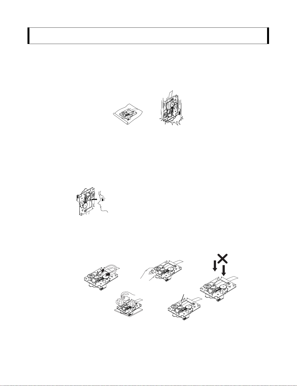
NOTES REGARDING HANDLING OF THE PICK-UP
1. Notes for transport and storage
1) The pick-up should always be left in its conductive bag until immediately prior to use.
2) The pick-up should never be subjected to external pressure or impact.
2. Repair notes
1) The pick-up incorporates a strong magnet, and so should never be brought close to magnetic materials.
2) The pick-up should always be handled correctly and carefully, taking care to avoid external pressure and
impact. If it is subjected to strong pressure or impact, the result may be an operational malfunction and/or
damage to the printed-circuit board.
3) Each and every pick-up is already individually adjusted to a high degree of precision, and for that reason
the adjustment point and installation screws should absolutely never be touched.
4) Laser beams may damage the eyes!
Absolutely never permit laser beams to enter the eyes!
Also NEVER switch ON the power to the laser output part (lens, etc.) of the pick-up if it is damaged.
5) Cleaning the lens surface
If there is dust on the lens surface, the dust should be cleaned away by using an air bush (such as used
for camera lens). The lens is held by a delicate spring. When cleaning the lens surface, therefore, a cotton swab should be used, taking care not to distort this.
6) Never attempt to disassemble the pick-up.
Spring by excess pressure. If the lens is extremely dirty, apply isopropyl alcohol to the cotton swab.
(Do not use any other liquid cleaners, because they will damage the lens.) Take care not to use too much
of this alcohol on the swab, and do not allow the alcohol to get inside the pick-up.
Storage in conductive bag
Drop impact
NEVER look directly at the laser beam, and don’t let
contact fingers or other exposed skin.
Magnet
How to hold the pick-up
Conductive Sheet
Cotton swab
Pressure
Pressure
SECTION 1. GENERAL
1-3
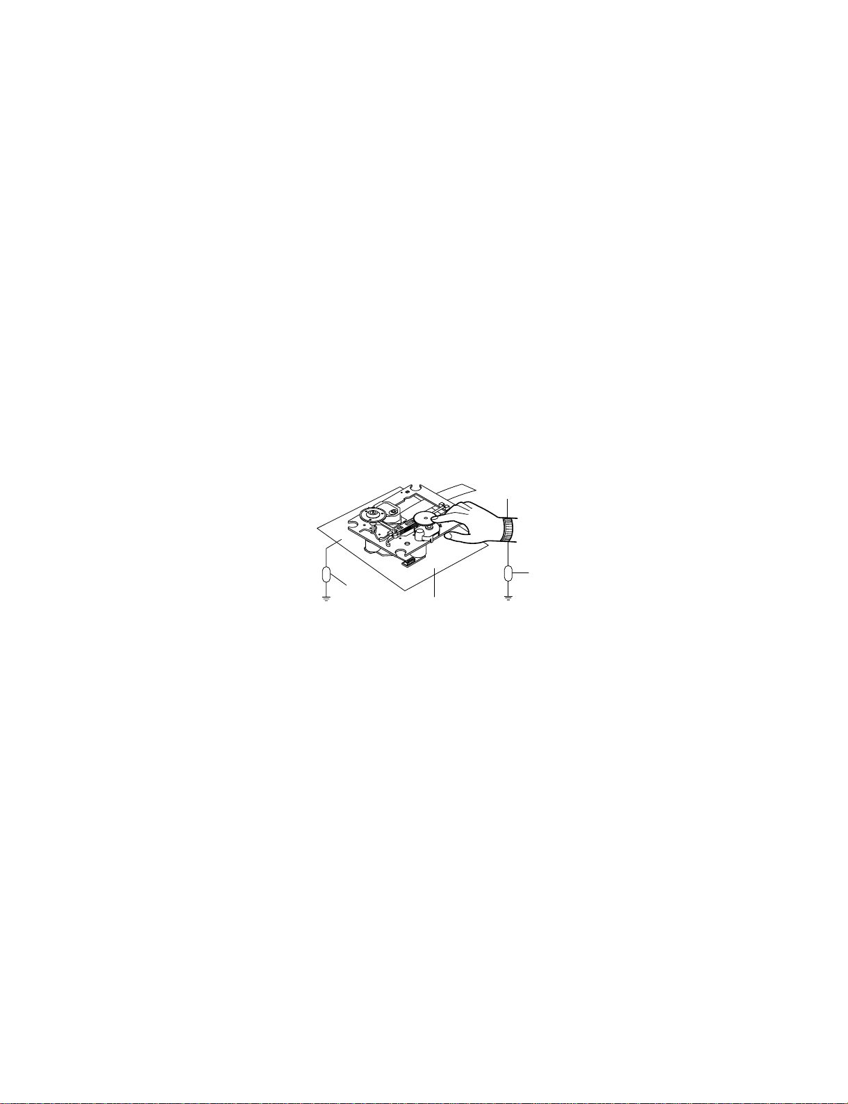
NOTES REGARDING COMPACT DISC PLAYER REPAIRS
1. Preparations
1) Compact disc players incorporate a great many ICs as well as the pick-up (laser diode). These components
are sensitive to, and easily affected by, static electricity. If such static electricity is high voltage, components
can be damaged, and for that reason components should be handled with care.
2) The pick-up is composed of many optical components and other high-precision components. Care must be
taken, therefore, to avoid repair or storage where the temperature of humidity is high, where strong magnetism is present, or where there is excessive dust.
2. Notes for repair
1) Before replacing a component part, first disconnect the power supply lead wire from the unit
2) All equipment, measuring instruments and tools must be grounded.
3) The workbench should be covered with a conductive sheet and grounded.
When removing the laser pick-up from its conductive bag, do not place the pick-up on the bag. (This is
because there is the possibility of damage by static electricity.)
4) To prevent AC leakage, the metal part of the soldering iron should be grounded.
5) Workers should be grounded by an armband (1M Ω)
6) Care should be taken not to permit the laser pick-up to come in contact with clothing, in order to prevent
static electricity changes in the clothing to escape from the armband.
7) The laser beam from the pick-up should NEVER be directly facing the eyes or bare skin.
Resistor
(1 Mohm)
Conductive
Sheet
Resistor
(1 Mohm)
Armband
1-4
ESD PRECAUTIONS
Electrostatically Sensitive Devices (ESD)
Some semiconductor (solid state) devices can be damaged easily by static electricity. Such components
commonly are called Electrostatically Sensitive Devices (ESD). Examples of typical ESD devices are integrated
circuits and some field-effect transistors and semiconductor chip components. The following techniques should
be used to help reduce the incidence of component damage caused by static electricity.
1. Immediately before handling any semiconductor component or semiconductor-equipped assembly, drain off
any electrostatic charge on your body by touching a known earth ground. Alternatively, obtain and wear a
commercially available discharging wrist strap device, which should be removed for potential shock reasons
prior to applying power to the unit under test.
2. After removing an electrical assembly equipped with ESD devices, place the assembly on a conductive surface
such as aluminum foil, to prevent electrostatic charge buildup or exposure of the assembly.
3. Use only a grounded-tip soldering iron to solder or unsolder ESD devices.
4. Use only an anti-static solder removal device. Some solder removal devices not classified as "anti-static" can
generate electrical charges sufficient to damage ESD devices.
5. Do not use freon-propelled chemicals. These can generate electrical charges sufficient to damage ESD
devices.
6. Do not remove a replacement ESD device from its protective package until immediately before you are
ready to install it. (Most replacement ESD devices are packaged with leads electrically shorted together by
conductive foam, aluminum foil or comparable conductive materials).
7. Immediately before removing the protective material from the leads of a replacement ESD device, touch the
protective material to the chassis or circuit assembly into which the device will by installed.
CAUTION : BE SURE NO POWER IS APPLIED TO THE CHASSIS OR CIRCUIT, AND OBSERVE ALLOTHER
SAFETY PRECAUTIONS.
8. Minimize bodily motions when handing unpackaged replacement ESD devices. (Otherwise harmless motion
such as the brushing together of your clothes fabric or the lifting of your foot from a carpeted floor can generate static electricity sufficient to damage an ESD device).
CAUTION. GRAPHIC SYMBOLS
THE LIGHTNING FLASH WITH APROWHEAD SYMBOL. WITHIN AN EQUILATERAL TRIANGLE, IS
INTENDED TO ALERT THE SERVICE PERSONNELTO THE PRESENCE OF UNINSULATED
“DANGEROUS VOLTAGE” THAT MAY BE OF SUFFICIENT MAGNITUDE TO CONSTITUTE A RISK OF
ELECTRIC SHOCK.
THE EXCLAMATION POINTWITHIN AN EQUILATERAL TRIANGLE IS INTENDED TO ALERT THE
SERVICE PERSONNEL TO THE PRESENCE OF IMPORTANT SAFETY INFORMATION IN SERVICE
LITERATURE.

1-5
SERVICE INFORMATION FOR EEPROM
POWER ON
DVD LOGO Status (NO Disk status)
Remotecontrol
Pause key-->1-->4-->7-->2 in order.
Press number 0~9, Press charater
A~F (1~6 for a while)
Use arrow key ( ) to
move to approprite position and
make changes
Press pause key once
Change will be applied when power
OFF-->ON.
* OPTION
• NTSC model doesn’t have VCR option and use DVD option B~F as VCR option. (only DVD exist)
• PAL model has another separate VCR option. (Both VCR and DVD exist)
NAME HEX
OPT 1 55
OPT 2 41
OPT 3 40
OPT 4 FF
OPT 5 52
OPT 6 05
OPT 7 F8
OPT 8 31
OPT 9 0C
OPT A 00
OPT B 00
OPT C 00
OPT D 00
OPT E 00
OPT F 00
OPT G 00
DETECT NEW EEPROM
(OPTION EDIT SCREEN)
* Refer to page 6-1.

1-6
SPECIFICATIONS
GENERAL
Power supply Refer to main label
Power consumption Refer to main label
Net Weight 3.9 kg
External dimensions (W x H x D) 430 x 57 x 295 mm
Operating conditions Temperature: 5°C to 35°C, Operation status: Horizontal
Operating humidity 5% to 85%
CD/DVD
Laser Semiconductor laser, wavelength 650 nm
Signal system PAL 625/50, NTSC 525/60
Frequency response (audio) 150 Hz to 18 kHz
Signal-to-noise ratio (audio) More than 75 dB (1 kHz, NOP -6 dB, 20 kHz LPF/A-Filter)
Dynamic range (audio) More than 70 dB
Harmonic distortion (audio) 0.5 % (1 kHz, at 1W position) (20 kHz LPF)
VIDEO
Video input 1.0 V (p-p), 75 Ω, negative sync., RCAjack x 1
Video output 1.0 V (p-p), 75 Ω, negative sync., RCA jack x 1/ SCART (TO TV)
TUNER
FM
Tuning Range 87.5 - 108.0 MHz or 65.0 - 74.0 MHz, 87.5 - 108.0 MHz
Intermediate Frequency 10.7 MHz
Signal-to Noise Ratio 60 dB (Mono)
Frequency Response 140 - 8,000 Hz
AM [MW]
Tuning Range 522 - 1,620 kHz or 520 - 1,720 kHz
Intermediate Frequency 450 kHz
AMPLIFIER(LH-T26’s)
Stereo mode Front: 30 W + 30 W (THD 10 %)
Centre*: 30 W
Surround*: 30 W + 30 W (6Ω at 1 kHz, THD 10 %)
Subwoofer*: 70 W (8Ω at 30 Hz, THD 10 %)
Input AUX IN, MIC
Outputs MONITOR, PHONES: (32 Ω, 1.0 V)
SPEAKERS(LHS-26SG)
Satellite Speaker Passive Subwoofer
Type 1 Way 1 Speaker 1 Way 1 Speaker
Impedance 6 Ω 8 Ω
Frequency Response 130 - 20,000 Hz 50 - 1,500 Hz
Sound Pressure Level 83 dB/W (1m) 82 dB/W (1m)
Rated Input Power 30W 70W
Max. Input Power 60W 140W
Net Dimensions 88 x 100 x 95 mm 160 x 350 x 325 mm
Net Weight 0.54 kg 4.12 kg
(* Depending on the sound mode
settings and the source, there may
be no sound output.)

1-7
SPEAKERS(LHS-26SH)
Satellite Speaker Passive Subwoofer
Type 1 Way 1Speakers 1 Way 1Speaker
Impedance 6 Ω 8 Ω
Frequency Response 130 - 20,000 Hz 50 - 1,500 Hz
Sound Pressure Level 130 - 20,000 Hz 50 - 1,500 Hz
Rated Input Power 30W 70W
Max Input Power 60W 140W
Net Dimensions 88 x 100 x 95 mm 160 x 350 x 325 mm
Net Weight 0.54 kg 4.12 kg
SPEAKERS(LHS-26SQ)
Satellite Speaker Passive Subwoofer
Type 1 Way 1 Speaker 1 Way 1 Speaker
Impedance 6 Ω 8 Ω
Frequency Response 130 - 20,000 Hz 50 - 1,500 Hz
Sound Pressure Level 83 dB/W (1m) 82 dB/W (1m)
Rated Input Power 30W 70W
Max. Input Power 60W 140W
Net Dimensions 88 x 100 x 95 mm 160 x 350 x 325 mm
Net Weight 0.54 kg 4.12 kg
2-1
SECTION 2. AUDIO PART
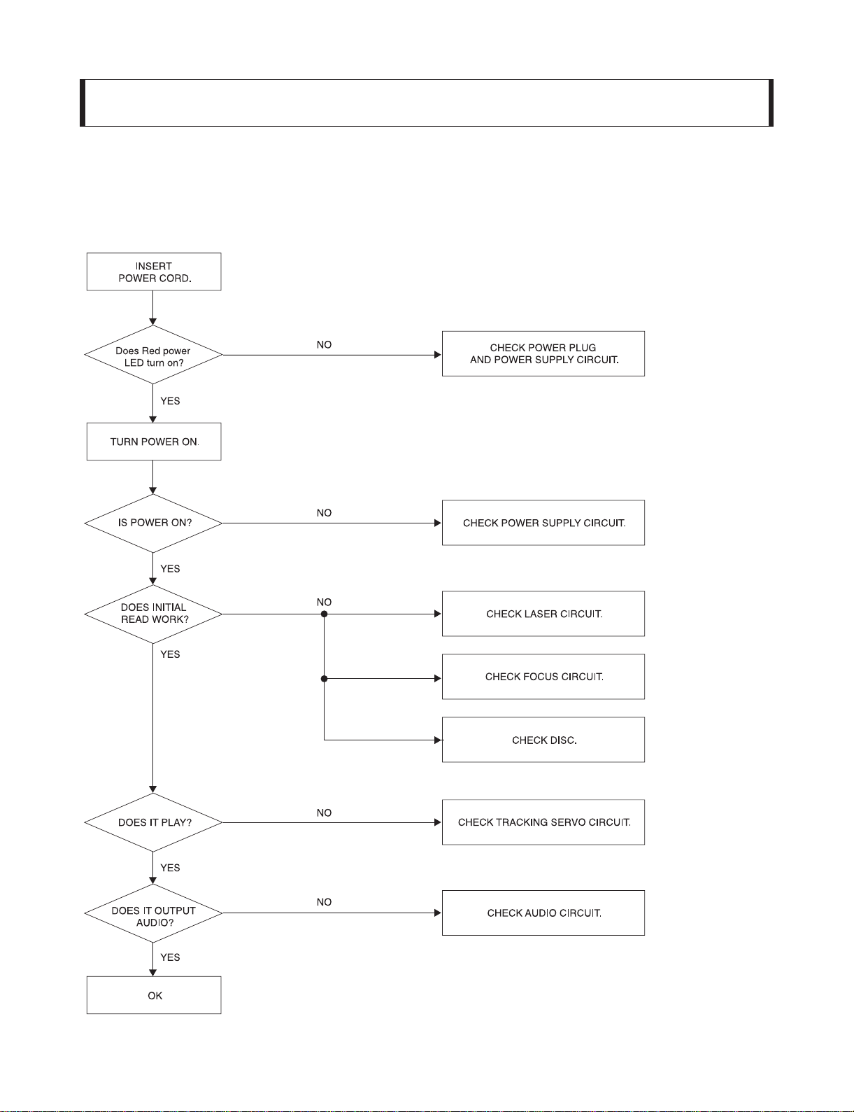
AUDIO TROUBLESHOOTING GUIDE
1. POWER SUPPLY CIRCUIT
2-2
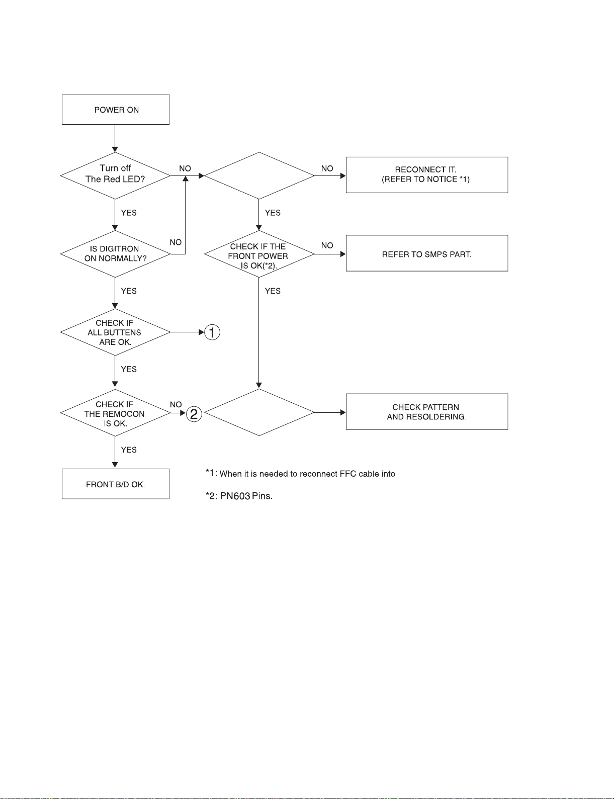
2. FRONT CIRCUIT (1/2)
THE P1301 IS OK?
CHECK IF
CHECK IF
THE DIS301 IS OK?
P1301
Short 1pin of CN901 with 4pin of CN901 in SMPS part.
PIN1
PIN2
PIN3
PIN12
: -41 VKK
: -22 FL+
: -26.5 FL-
: +5.0
2-3
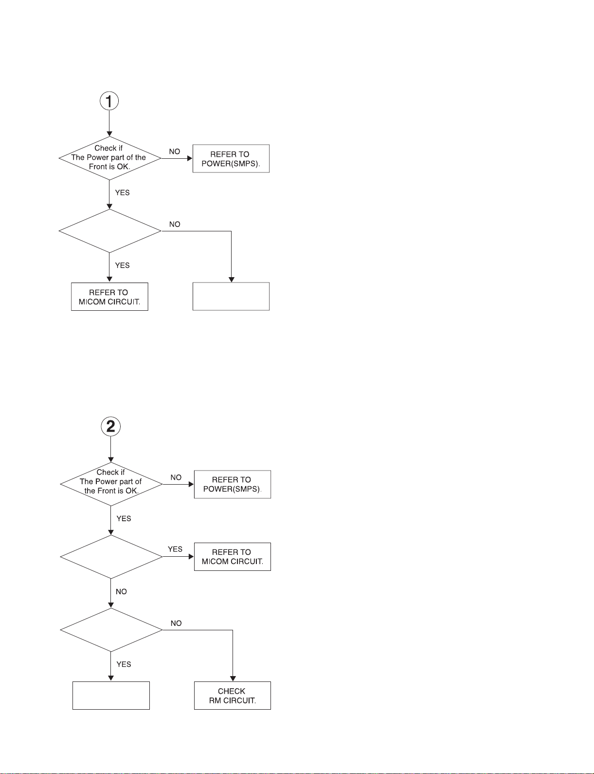
3. FRONT CIRCUIT (2/2)
CHECK IF
R345 ~ R350, R154
OK.
REPLACE
R345 ~ R350, R154.
Check if
the Remocon
waceform of the
P3101 pin 10
is OK
Check if
the RM301
voltage is OK(5V)
Resoldering or
Replace RM301
2-4 2-5
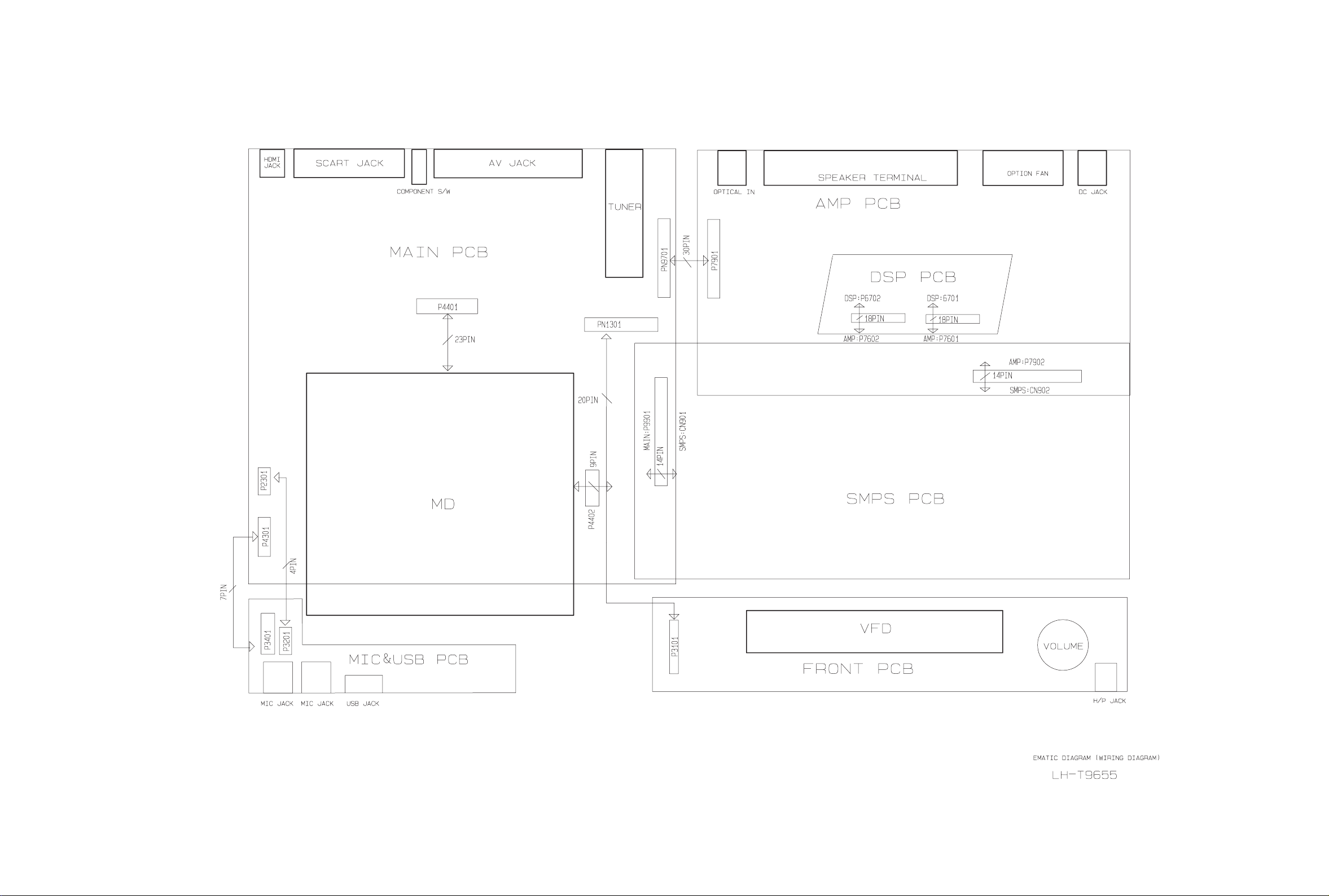
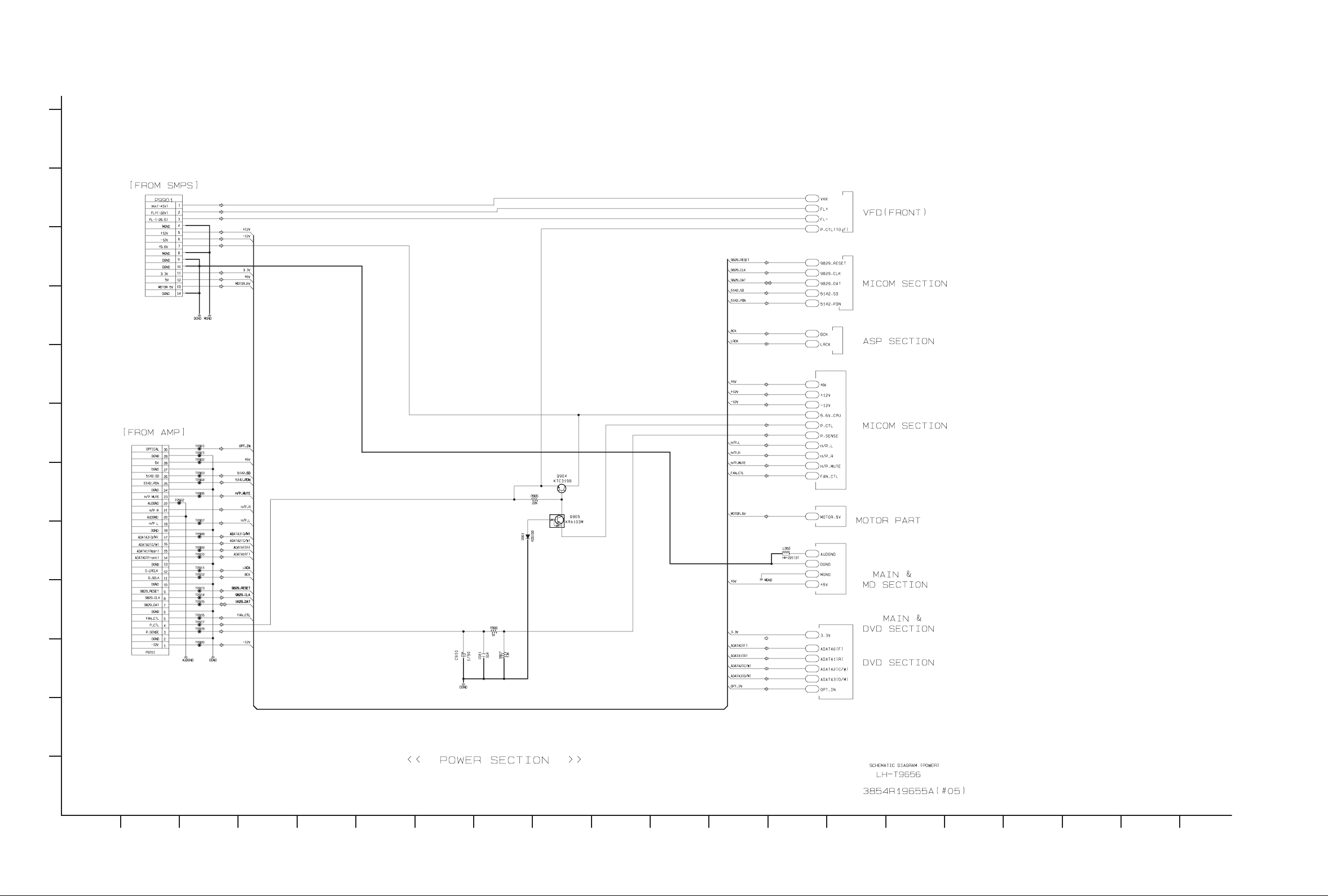
WIRING DIAGRAM
2-6 2-7
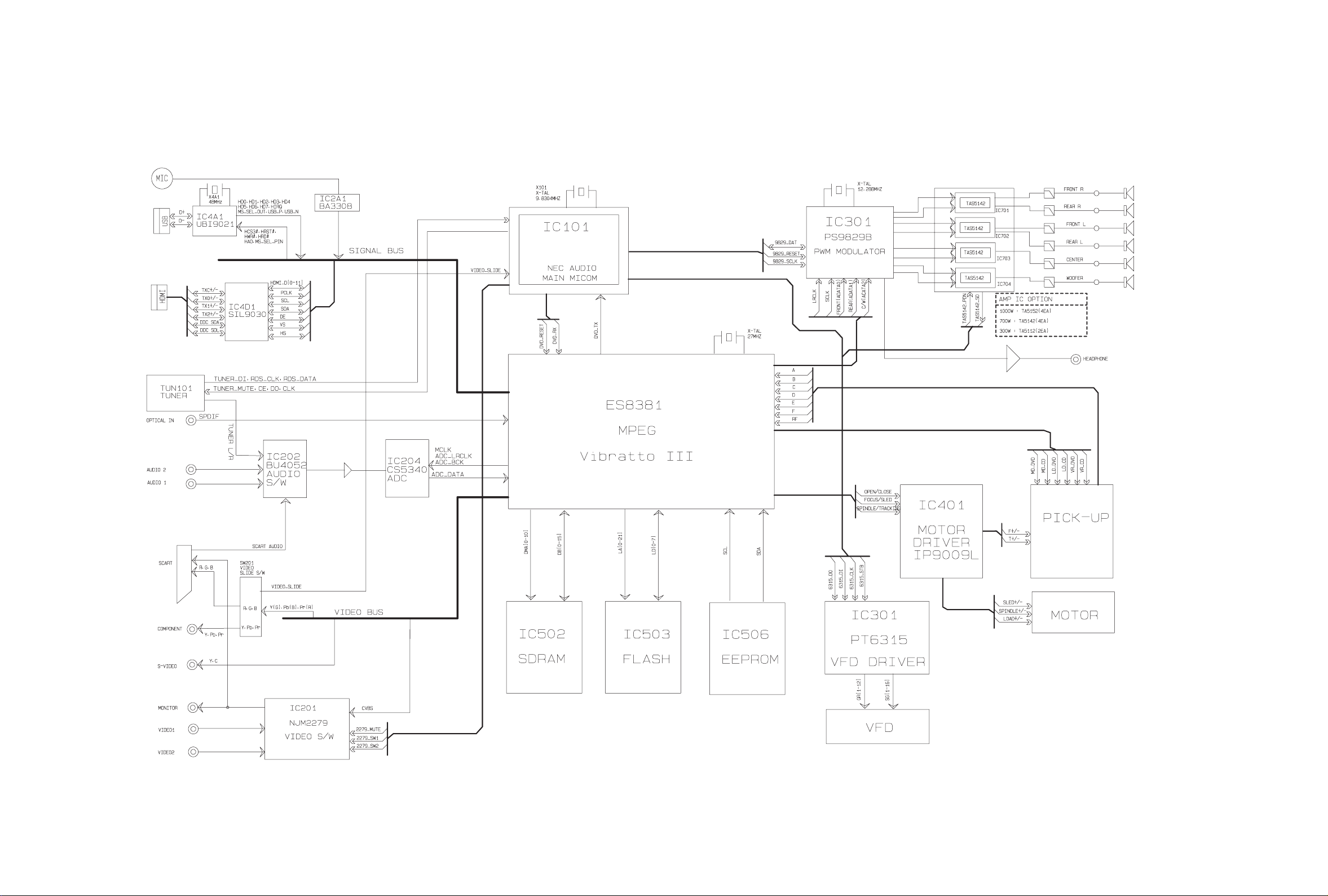
BLOCK DIAGRAM
2-8 2-9
CIRCUIT DIAGRAMS
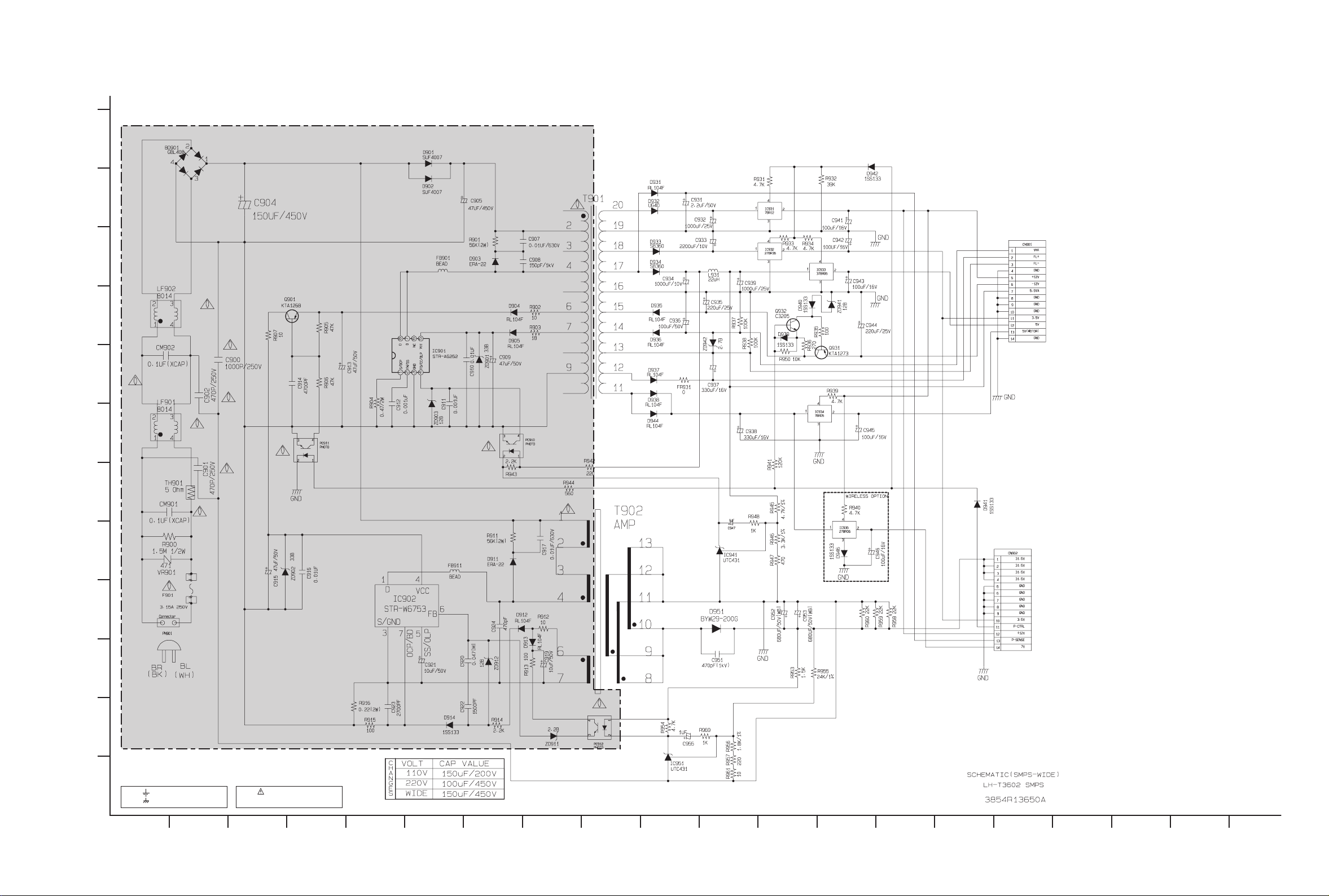
1. SMPS(POWER) CIRCUIT DIAGRAM
NOTES) Symbol denotes AC ground.
NOTES) Symbol denotes DC chassis ground.
NOTE) Warning
NOTE) Parts that are shaded are critical
NOTE) With respect to risk of fire or
NOTE) electricial shock.
A
1
2
3
4
5
6
7
8
9
10
11
12
B C D E F G H I J K L M N O P Q R ST
2-10 2-11
2. POWER INTERFACE CIRCUIT DIAGRAM
A
1
2
3
4
5
6
7
8
9
10
11
12
B C D E F G H I J K L M N O P Q R ST
2-12 2-13
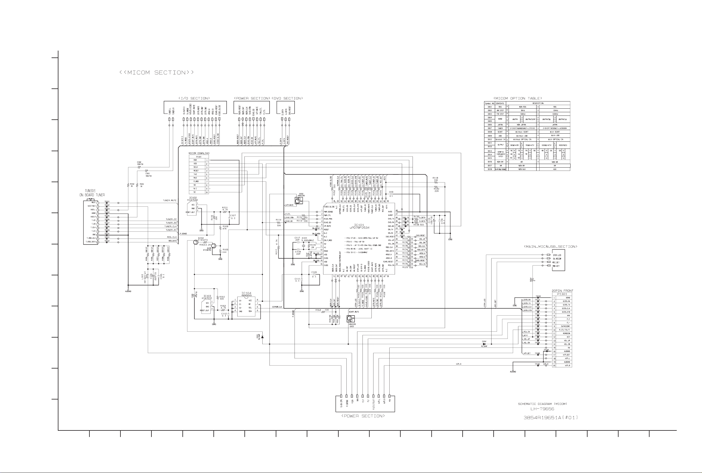
3. µ-COM(MAIN) CIRCUIT DIAGRAM
A
1
2
3
4
5
6
7
8
9
10
11
12
B C D E F G H I J K L M N O P Q R ST
2-14 2-15
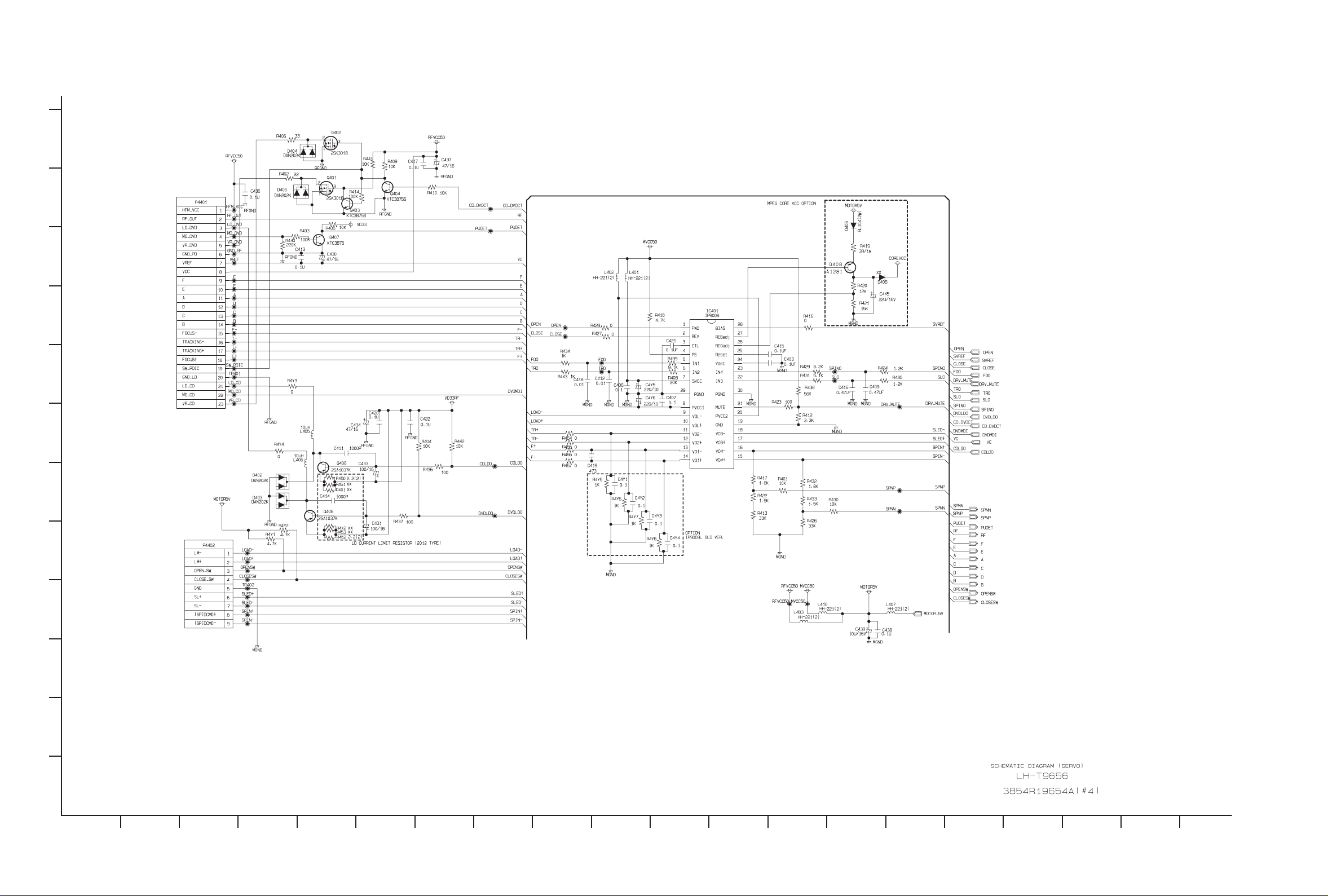
4. SERVO CIRCUIT DIAGRAM
A
1
2
3
4
5
6
7
8
9
10
11
12
B C D E F G H I J K L M N O P Q R ST
2-16 2-17
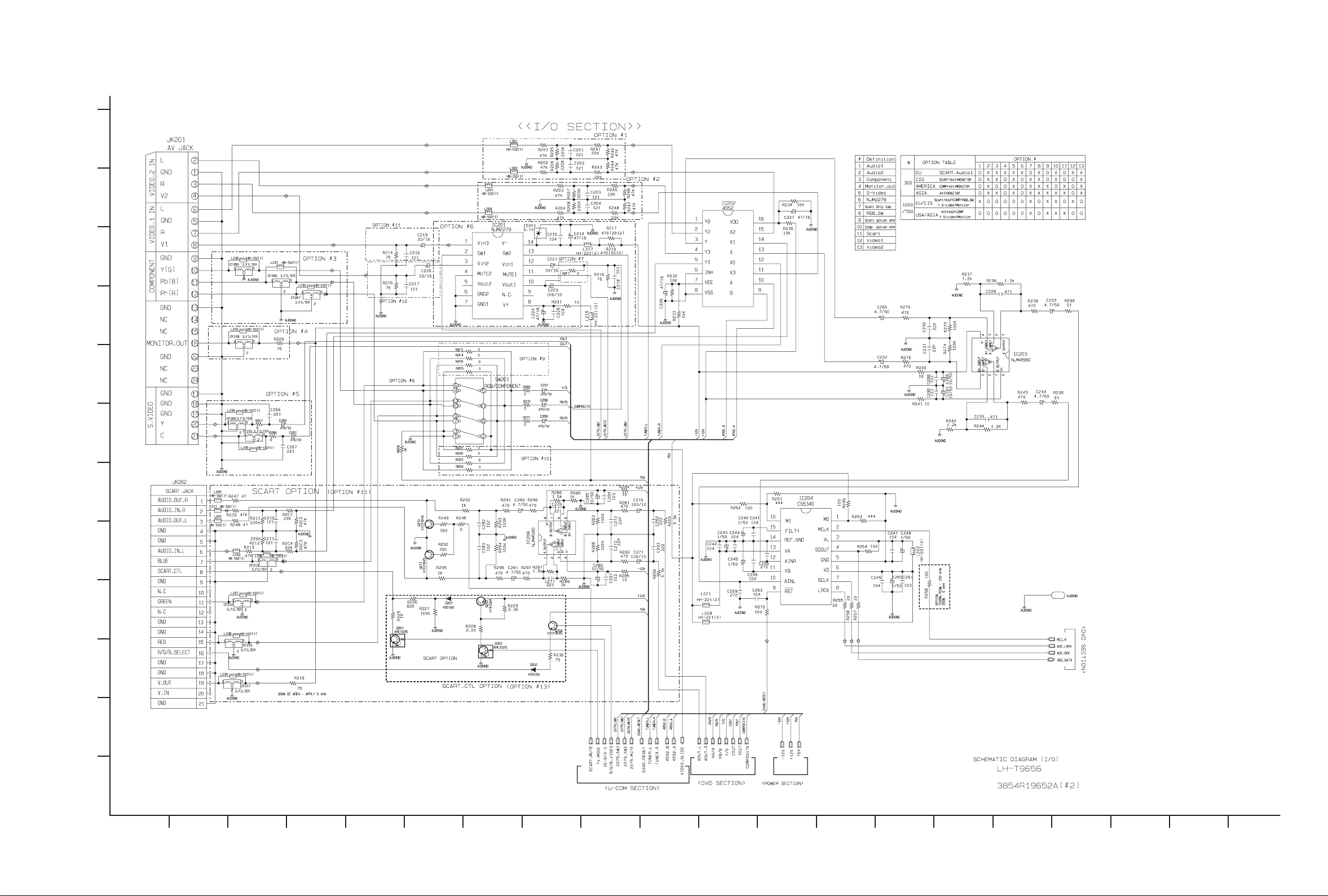
5. I/O CIRCUIT DIAGRAM
A
1
2
3
4
5
6
7
8
9
10
11
12
B C D E F G H I J K L M N O P Q R ST

2-18 2-19
6. MIC CIRCUIT DIAGRAM
A
1
2
3
4
5
6
7
8
9
10
11
12
B C D E F G H I J K L M N O P Q R ST
 Loading...