

Page 1

P/NO : AFN77255292 JULY, 2015
(LAS950M, S95A1-D)
CAUTION
BEFORE SERVICING THE UNIT, READ THE “SAFETY PRECAUTIONS”
IN THIS MANUAL.
Website http://biz.lgservice.com
Internal Use Only
MODEL: LAS950M (LAS950M, S95A1-D)SERVICE MANUAL
Smart Hi-Fi Audio Wireless
Multi-room Sound Bar
SERVICE MANUAL
MODEL: LAS950M
Page 2

CONTENTS
SECTION 1 ........ SUMMARY
SECTION 2 ........ ELECTRICAL
SECTION 3 ........ CABINET & MAIN CHASSIS
SECTION 4 ........ WIRELESS SUBWOOFER PART
SECTION 5 ........ REPLACEMENT PARTS LIST
1-1
Page 3

SECTION 1
SUMMARY
CONTENTS
PRODUCT SAFETY SERVICING GUIDELINES FOR AUDIO PRODUCTS .............................................. 1-3
SERVICING PRECAUTIONS .......................................................................................................................... 1-4
• GENERAL SERVICING PRECAUTIONS
• INSULATION CHECKING PRODEDURE
• ELECTROSTATICALLY SENSITIVE (ES) DEVICES
WIRELESS SUBWOOFER CONNECTION ................................................................................................... 1-5
LAN UPDATE GUIDE ...................................................................................................................................... 1-6
SOFTWARE UPDATE GUIDE ...................................................................................................................... 1-10
HOW TO WIRELESS FACTORY RESET & PAIRING ............................................................................... 1-14
HIDDEN MODE ............................................................................................................................................... 1-14
VERSION CHECK .......................................................................................................................................... 1-15
OPTION EDIT GUIDE .................................................................................................................................... 1-16
SPECIFICATIONS .......................................................................................................................................... 1-17
1-2
Page 4
PRODUCT SAFETY SERVICING GUIDELINES
FOR AUDIO PRODUCTS
IMPORTANT SAFETY NOTICE
This manual was prepared for use only by properly trained audio-video service
technicians.
When servicing this product, under no circumstances should the original design be
modified or altered without permission from LG Corporation. All components should
be replaced only with types identical to those in the original circuit and their physical
location, wiring and lead dress must conform to original layout upon completion of
repairs.
Special components are also used to prevent x-radiation, shock and fire hazard.
These components are indicated by the letter “x” included in their component designators and are required to maintain safe performance. No deviations are allowed
without prior approval by LG Corporation.
Circuit diagrams may occasionally differ from the actual circuit used. This way, implementation of the latest safety and performance improvement changes into the set is
not delayed until the new service literature is printed.
CAUTION : Do not attempt to modify this product in any way. Never perform cus-
tomized installations without manufacturer’s approval. Unauthorized modifications
will not only void the warranty, but may lead to property damage or user injury.
Service work should be performed only after you are thoroughly familiar with these
safety checks and servicing guidelines.
GRAPHIC SYMBOLS
The exclamation point within an equilateral triangle is intended to alert
the service personnel to important safety information in the service
literature.
The lightning flash with arrowhead symbol within an equilateral
triangle is intended to alert the service personnel to the presence of
noninsulated “dangerous voltage” that may be of sufficient magnitude
to constitute a risk of electric shock.
The pictorial representation of a fuse and its rating within an equilateral triangle is intended to convey to the service personnel the following fuse replacement caution notice:
CAUTION : FOR CONTINUED PROTECTION AGAINST RISK
OF FIRE, REPLACE ALL FUSES WITH THE SAME TYPE AND
RATING AS MARKED NEAR EACH FUSE.
SERVICE INFORMATION
While servicing, use an isolation transformer for protection from AC line shock. After
the original service problem has been corrected, make a check of the following:
FIRE AND SHOCK HAZARD
1. Be sure that all components are positioned to avoid a possibility of adjacent component shorts. This is especially important on items trans-ported to and from the
repair shop.
2. Verify that all protective devices such as insulators, barriers, covers, shields, strain
reliefs, power supply cords, and other hardware have been reinstalled per the
original design. Be sure that the safety purpose of the polarized line plug has not
been defeated.
3. Soldering must be inspected to discover possible cold solder joints, solder
splashes, or sharp solder points. Be certain to remove all loose foreign particles.
4. Check for physical evidence of damage or deterioration to parts and components,
for frayed leads or damaged insulation (including the AC cord), and replace if
necessary.
5. No lead or component should touch a high current device or a resistor rated at 1
watt or more. Lead tension around protruding metal surfaces must be avoided.
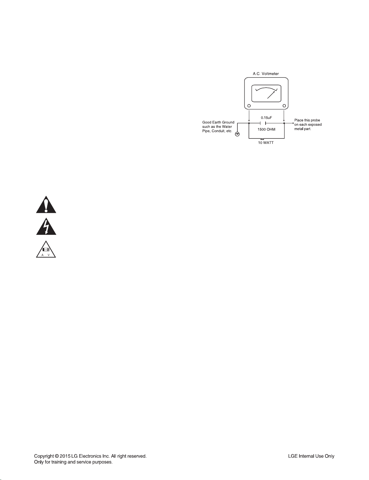
6. After reassembly of the set, always perform an AC leakage test on all exposed
metallic parts of the cabinet (the channel selector knobs, antenna terminals,
handle and screws) to be sure that set is safe to operate without danger of electrical shock. DO NOT USE A LINE ISOLATION TRANSFORMER DURING THIS
TEST. Use an AC voltmeter having 5000 ohms per volt or more sensitivity in the
following manner: Connect a 1500 ohm, 10 watt resistor, paralleled by a .15 mfd
150V AC type capacitor between a known good earth ground water pipe, conduit, etc.) and the exposed metallic parts, one at a time. Measure the AC voltage
across the combination of 1500 ohm resistor and .15 mfd capacitor. Reverse the
AC plug by using a non-polarized adaptor and repeat AC voltage measurements
for each exposed metallic part. Voltage measured must not exceed 0.75 volts
RMS. This corresponds to 0.5 milliamp AC. Any value exceeding this limit constitutes a potential shock hazard and must be corrected immediately.
TIPS ON PROPER INSTALLATION
1. Never install any receiver in a closed-in recess, cubbyhole, or closely fitting shelf
space over, or close to, a heat duct, or in the path of heated air flow.
2. Avoid conditions of high humidity such as: outdoor patio installations where dew
is a factor, near steam radiators where steam leakage is a factor, etc.
3. Avoid placement where draperies may obstruct venting. The customer should
also avoid the use of decorative scarves or other coverings that might obstruct
ventilation.
4. Wall- and shelf-mounted installations using a commercial mounting kit must follow
the factory-approved mounting instructions. A product mounted to a shelf or platform must retain its original feet (or the equivalent thickness in spacers) to provide
adequate air flow across the bottom. Bolts or screws used for fasteners must not
touch any parts or wiring. Perform leakage tests on customized installations.
5. Caution customers against mounting a product on a sloping shelf or in a tilted
position, unless the receiver is properly secured.
6. A product on a roll-about cart should be stable in its mounting to the cart.
Caution the customer on the hazards of trying to roll a cart with small casters
across thresholds or deep pile carpets.
7. Caution customers against using extension cords. Explain that a forest of extensions, sprouting from a single outlet, can lead to disastrous consequences to
home and family.
1-3
Page 5

SERVICING PRECAUTIONS
CAUTION: Before servicing the
service data and its supplements and addends, read and follow the SAFETY PRECAUTIONS.
NOTE: if unforeseen circumstances create conflict between
the following servicing precautions and any of the safety
precautions in this publication, always follow the safety precautions.
Remember Safety First :
General Servicing Precautions
1. Always unplug the
AC power source before:
(1) Removing or reinstalling any component, circuit board,
module, or any other assembly.
(2) Disconnecting or reconnecting any internal electrical
plug or other electrical connection.
(3) Connecting a test substitute in parallel with an electro-
lytic capacitor.
Caution: A wrong part substitution or incorrect polarity
installation of electrolytic capacitors may result in an
explosion hazard.
2. Do not spray chemicals on or near this
of its assemblies.
3. Unless specified otherwise in this service data, clean electrical contacts by applying an appropriate contact cleaning
solution to the contacts with a pipe cleaner, cotton-tipped
swab, or comparable soft applicator.
Unless specified otherwise in this service data, lubrication
of contacts is not required.
4. Do not defeat any plug/socket B+ voltage interlocks with
which instruments covered by this service manual might be
equipped.
5. Do not apply AC power to this
of its electrical assemblies unless all solid state device heat
sinks are correctly installed.
6. Always connect the test instrument ground lead to an
appropriate ground before connecting the test instrument
positive lead. Always remove the test instrument ground
lead last.
Insulation Checking Procedure
Disconnect the attachment plug from the AC outlet and turn
the power on. Connect an insulation resistance meter (500V)
to the blades of the attachment plug. The insulation resistance between each blade of the attachment plug and accessible conductive parts (Note 1) should be more than 1Mohm.
Note 1: Accessible Conductive Parts include Metal panels,
Input terminals, Earphone jacks,etc.
Audio products
Audio products
AC power cord from the
Audio products
covered by this
Audio products
and / or any
or any
Electrostatically Sensitive (ES) Devices
Some semiconductor (solid state) devices can be damaged
easily by static electricity. Such components commonly are
called Electrostatically Sensitive (ES) Devices. Examples
of typical ES devices are integrated circuits and some field
effect transistors and semiconductor chip components.
The following techniques should be used to help reduce the
incidence of component damage caused by static electricity.
1. Immediately before handling any semiconductor component or semiconductor-equipped assembly, drain off any
electrostatic charge on your body by touching a known
earth ground. Alternatively, obtain and wear a commercially available discharging wrist strap device, which should
be removed for potential shock reasons prior to applying
power to the unit under test.
2. After removing an electrical assembly equipped with ES
devices, place the assembly on a conductive surface such
as aluminum foil, to prevent electrostatic charge buildup or
exposure of the assembly.
3. Use only a grounded-tip soldering iron to solder or unsolder
ES devices.
4. Use only an anti-static solder removal device. Some solder
removal devices not classified as “anti-static” can generate
electrical charges sufficient to damage ES devices.
5. Do not use freon-propelled chemicals. These can generate
an electrical charge sufficient to damage ES devices.
6. Do not remove a replacement ES device from its protective
package until immediately before you are ready to install
it. (Most replacement ES devices are packaged with leads
electrically shorted together by conductive foam, aluminum
foil, or comparable conductive material).
7. Immediately before removing the protective material from
the leads of a replacement ES device, touch the protective
material to the chassis or circuit assembly into which the
device will be installed.
Caution: Be sure no power is applied to the chassis or cir-
cuit, and observe all other safety precautions.
8. Minimize bodily motions when handling unpackaged
replacement ES devices. (Normally harmless motion such
as the brushing together of your clothes fabric or the lifting
of your foot from a carpeted floor can generate static electricity sufficient to damage an ES device.)
1-4
Page 6
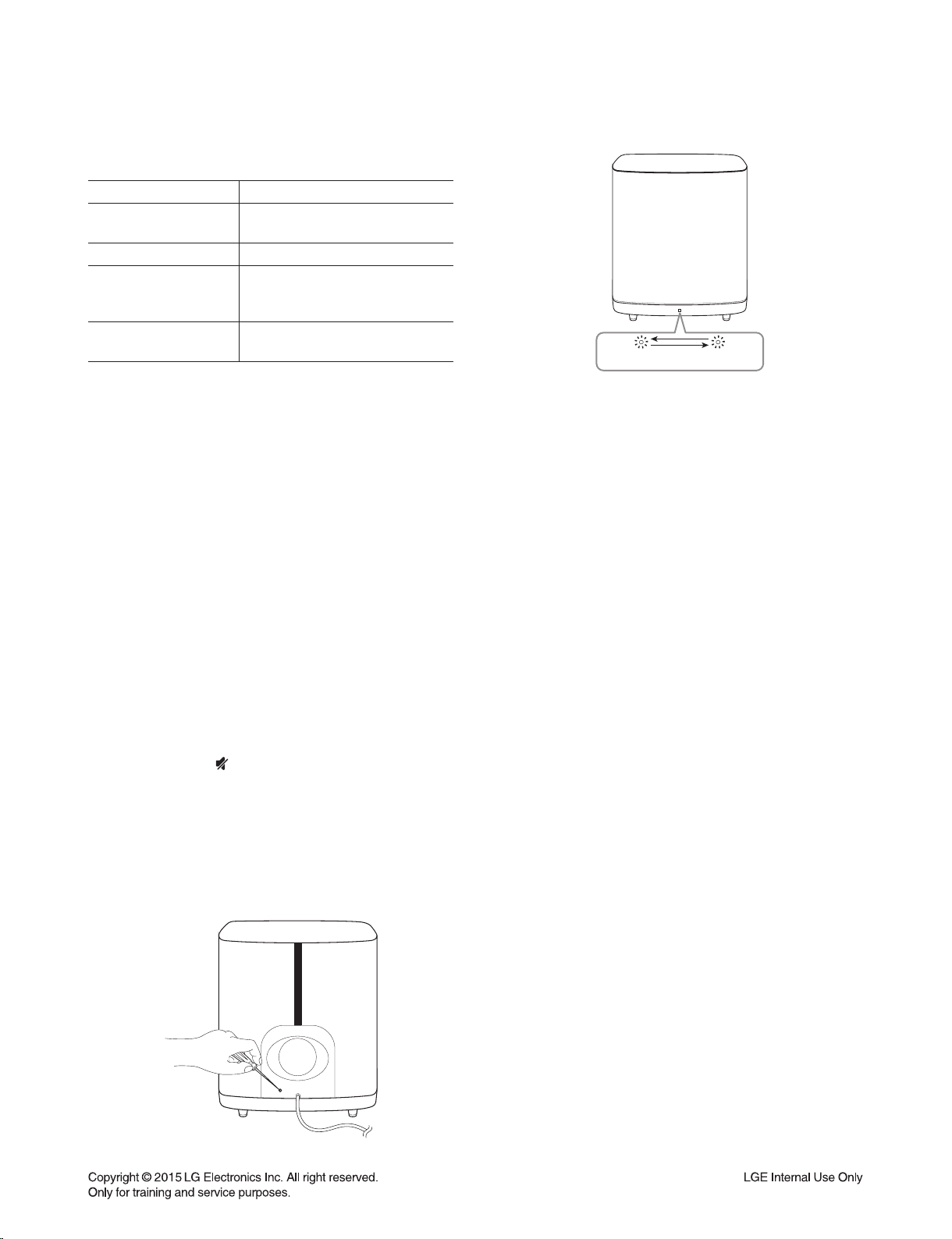
WIRELESS SUBWOOFER CONNECTION
LED indicator of wireless subwoofer
LED Color Status
Green
(Blink)
Green The connection is completed.
Red
Off
(No display)
Setting up the wireless subwoofer
for the fi rst time
1. Connect the power cord of the wireless subwoofer
to the outlet.
2. Turn on the main unit : The main unit and wireless
subwoofer will be automatically connected.
Manually pairing wireless subwoofer
When your connection is not completed, you can see
the red LED or the blinking of green LED on the wireless
subwoofer and the subwoofer does not make sound. To
solve the problem, follow the below steps.
1. Adjust volume level of the main unit to minimum.
- ”VOL MIN” appears on the display window.
2. Press and hold (Mute) on the remote control for
about 3 seconds.
- “WL RESET” appears on the display window briefl y.
3. If the LED of the wireless subwoofer already blinks
in green continually, you can skip this step.
Press and hold PAIRING on the back of the
wireless subwoofer for more than 5 seconds.
The connection is trying.
The wireless subwoofer is
in standby mode or the
connection is failed.
The power cord of wireless
subwoofer is disconnected.
- The LED of the wireless subwoofer lights up
alternately in red and green.
4. Disconnect the power cord of the main unit and the
wireless subwoofer.
5. Connect them again after the LED of the main unit
and the wireless subwoofer is fully turned off.
The main unit and the wireless subwoofer will be
paired automatically when you turn on the main
unit.
- When the connection is completed, you can see
the green LED on the subwoofer.
Note
:
• It takes a few seconds (and may take longer) for
the main unit and the subwoofer to communicate
with each other and make sounds.
• The closer the main unit and the subwoofer, the
better sound quality. It is recommended to install
the main unit and the subwoofer as close as
possible (within 5 m) and avoid the cases below.
- There is a obstacle between the main unit and the
subwoofer.
- There is a device using same frequency with this
wireless connection such as a medical equipment,
a microwave or a wireless LAN device.
1-5
Page 7
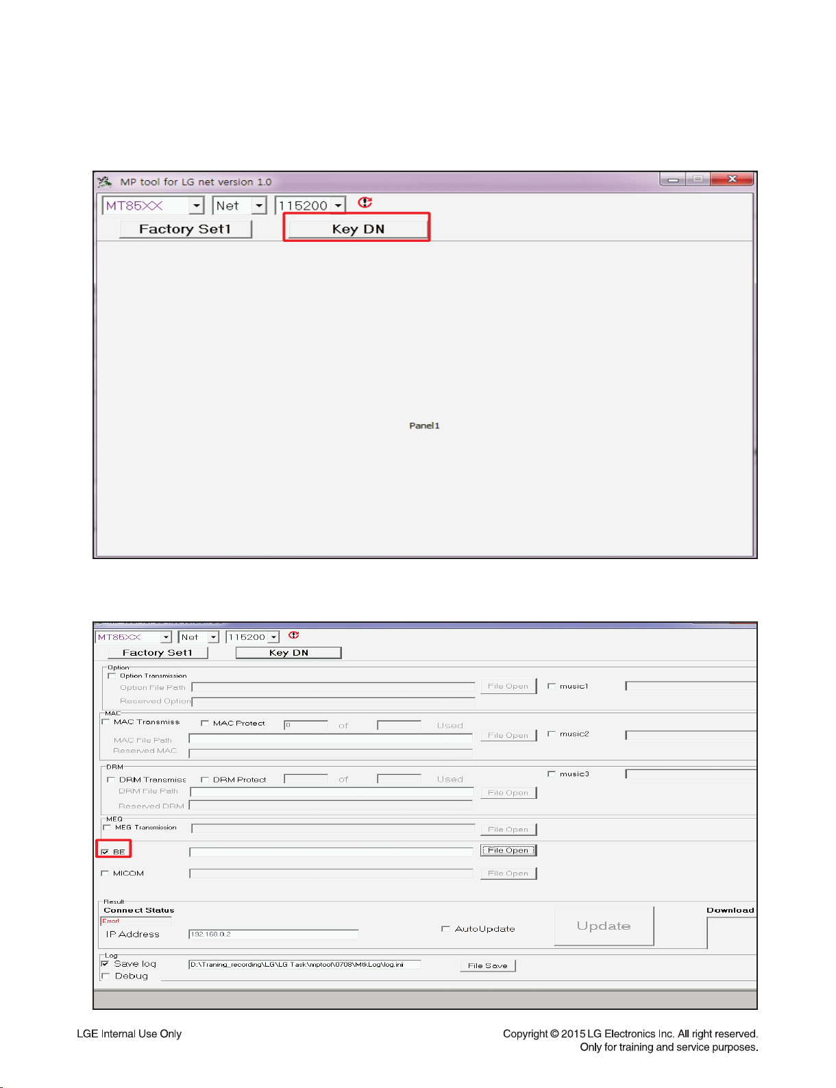
LAN UPDATE GUIDE
1. Using MP tool
1) Open MP tool and select “Key DN”.
2) Check the section for download and open download fi le.
1-6
Page 8
3) Connect PC and SET by cross LAN cable.
PC IP setting
IP: 192.168.0.1
Subnet: 255.255.254.0
Gateway: 10.168.0.1
4) Set power on.
5) Connect LAN cable to Set and then Press “ADD” key within 3 seconds after connect the LAN.
(Please connect the LAN when blinking WiFi-LED after booting)
*Download fi le name
B/E : LG_NB_9000M06.ROM
MICOM : MICOM_LAS950.HEX
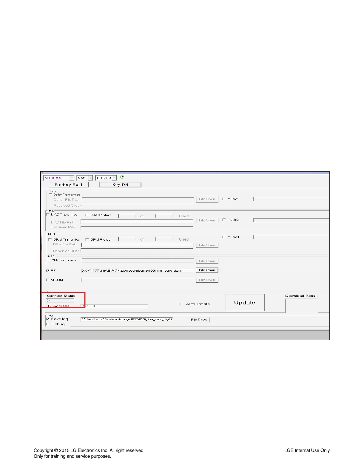
6) Connect Status change “OK!” if success connect MP tool.
1-7
Page 9
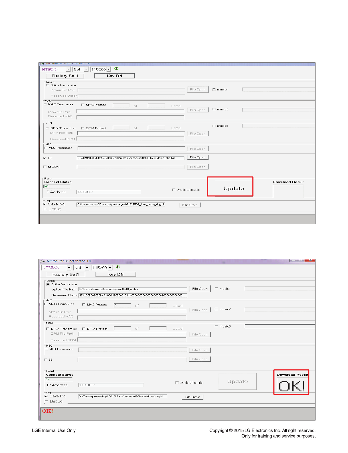
7) Press “Update” button.
8) Download result display “OK!” if start download.
1-8
Page 10
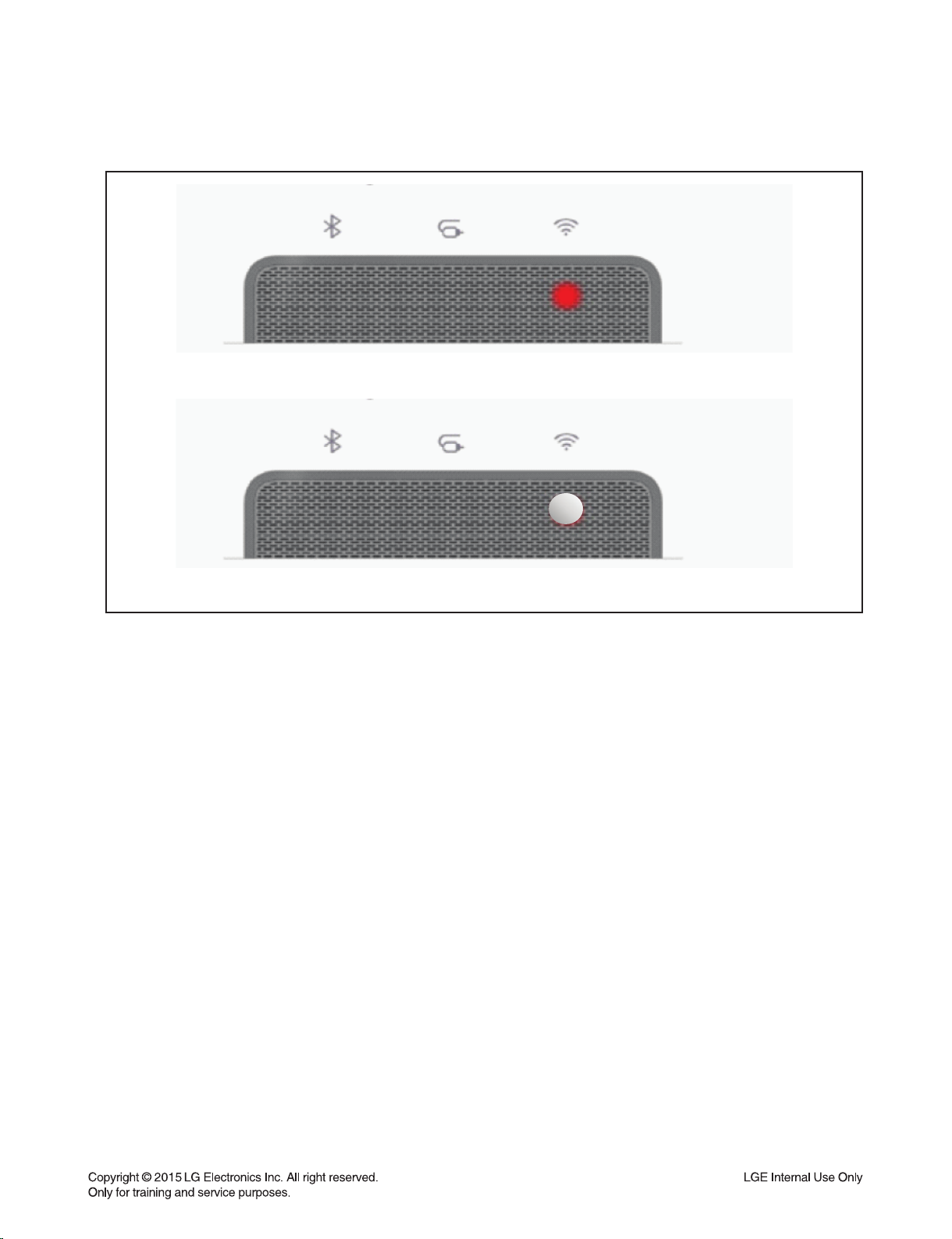
9) You can identify update status by network indicator lamp.
<Updating : blinking red LED>
<Complete update : blinking white LED>
1-9
Page 11

SOFTWARE UPDATE GUIDE
1. Using USB
1-1. MICOM
1) Copy the fi rmware to USB.
- Change the fi le name to “MICOM_LAS950.HEX”.
2) Insert USB to USB port.
3) VFD display “UPGRADE”.
4) Press “PLAY/PAUSE” key.
5) VFD display “M-UPDATE”.
6) Set auto power off after updating done.
1-2. MPEG
1) Copy the fi rmware to USB.
- Make the folder by “UPG_ALL” and copy fi rmware in “UPG_ALL” folder.
- Change the fi le name to “LG_NB_9000M06.ROM”.
2) Insert USB to USB port.
3) VFD display “UPGRADE”.
4) Press “PLAY/PAUSE” key.
5) VFD display “B-UPDATE”.
6) Set auto power off after updating done.
1-3. DSP
1) Copy the fi rmware to USB.
- Change the fi le name to “DSP_LAS950.HEX”.
2) Insert USB to USB port.
3) VFD display “UPGRADE”.
4) Press “PLAY/PAUSE” key.
5) VFD display “UPDATE”.
6) Return to the before function, after fi nished the updating.
1-4. EQ
1) Copy the fi rmware to USB.
- Change the fi le name to “EQ_PRG.BIN”.
2) Insert USB to USB port.
3) VFD display “UPGRADE”.
4) Press “PLAY/PAUSE” key.
5) VFD display “EQUPDATE”.
6) Set auto power off after fi nished the updating.
1-10
Page 12
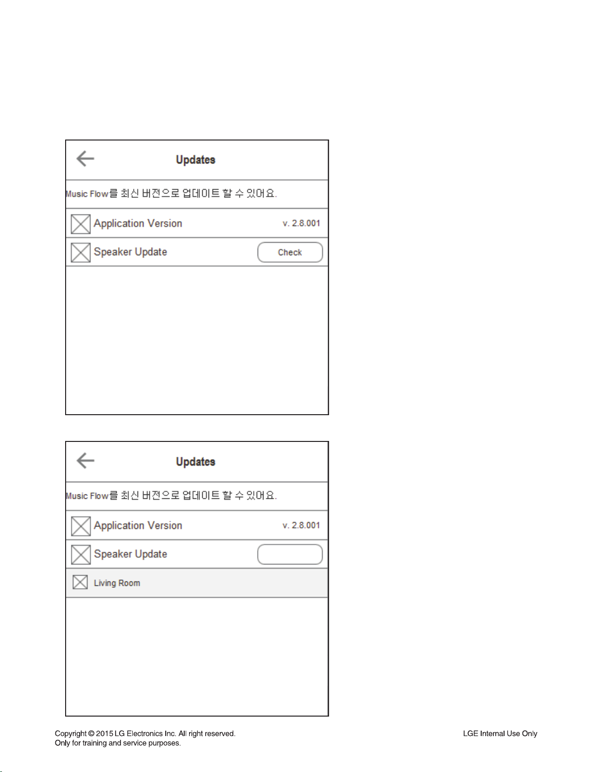
2. Using APP
1) Connect set and music fl ow app.
2) Select “setup update” menu then you can see below menu.
3) Enter “Check” button then display speaker list for update.
download
1-11
Page 13
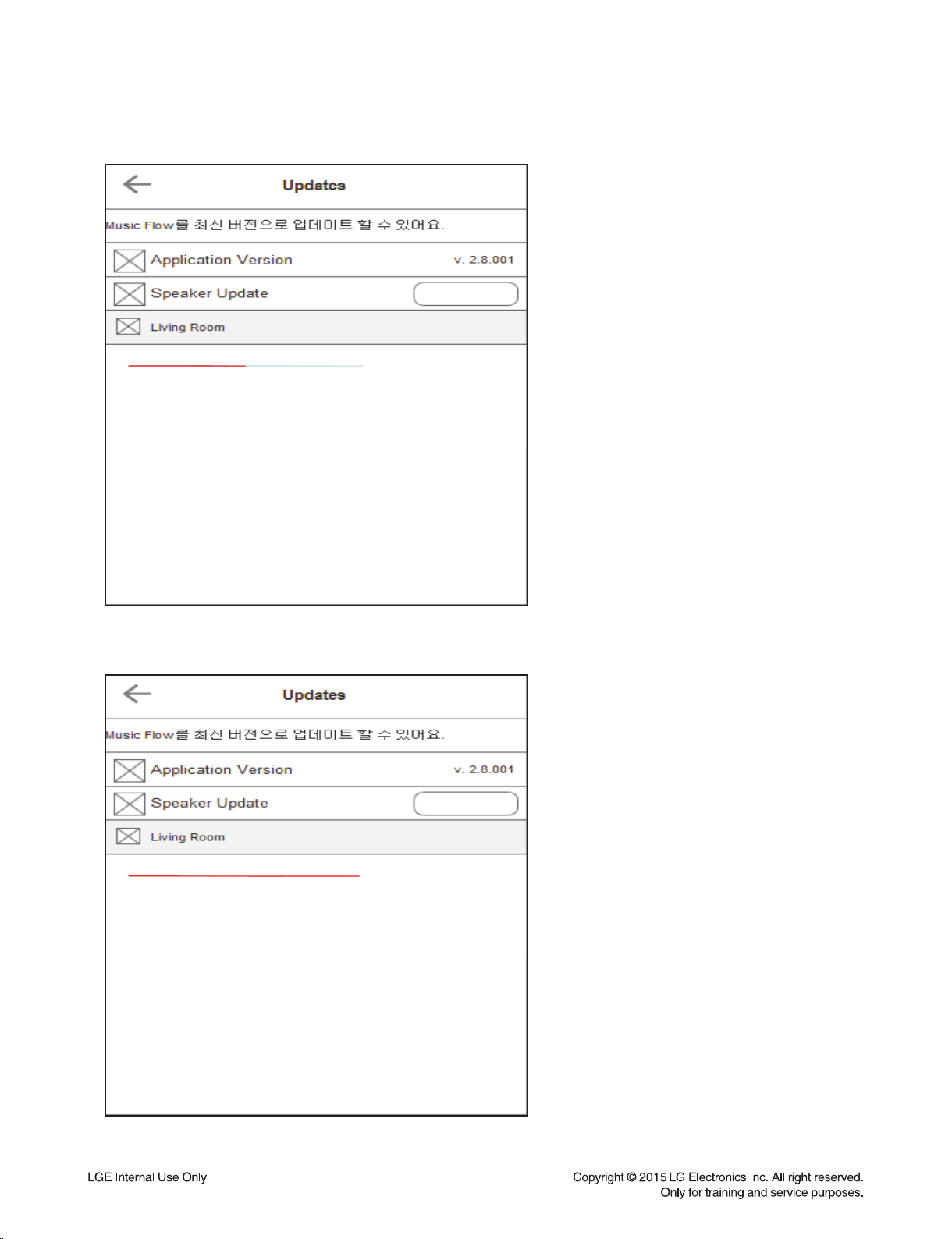
4) Enter “download” button then start download to speaker.
download
Downloading…
5) Display below menu after done download then enter “Ready” button for updating.
Ready
Do wnlo aded
1-12
Page 14
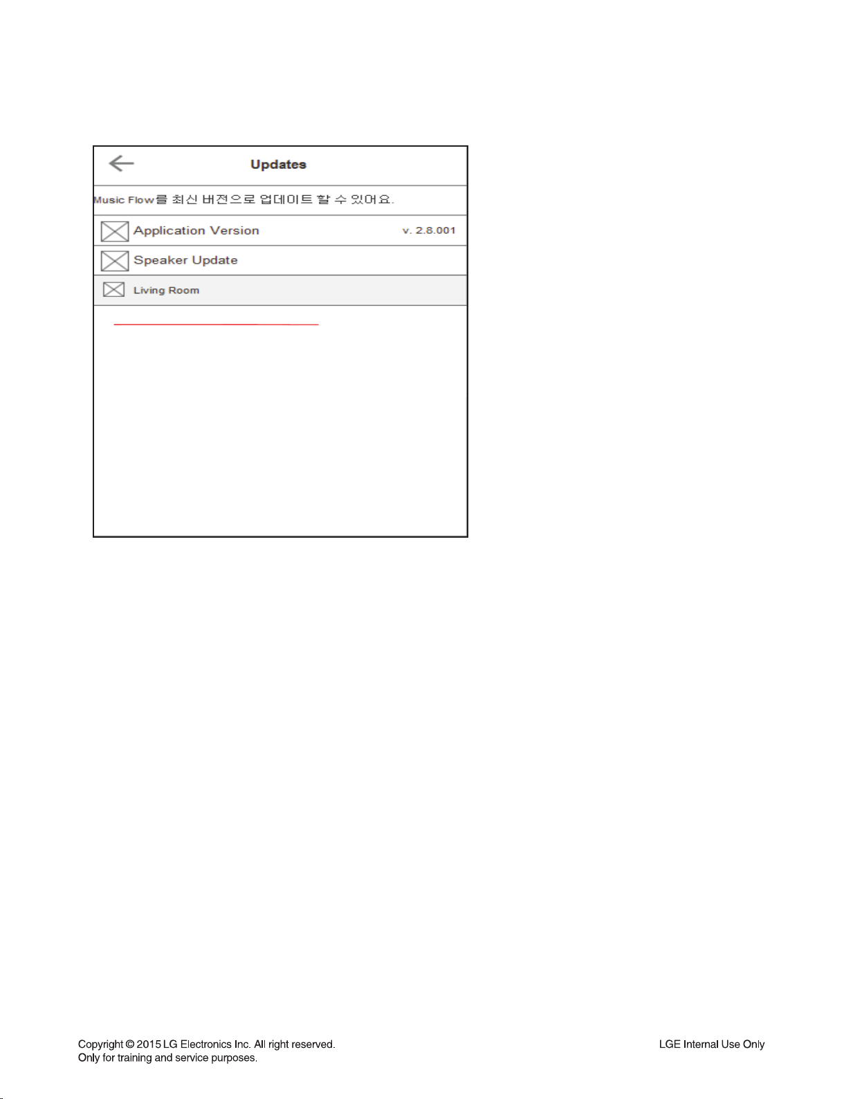
6) Display below menu after done update
Updated
7) Set rebooting. (Booting previous version if failed update.)
1-13
Page 15

HOW TO WIRELESS FACTORY RESET & PAIRING
1) Main set Wireless Reset.
- Volume Minimum state + Remote control “mute” for 5 seconds.
- Then, “WL RESET” will be displayed on the LCD.
2) Power off Main set.
3) Wireless Subwoofer: Wireless Reset.
- Press and hold PAIRING key on the back of the wireless subwoofer for more than 5 seconds.
- Then, LED will be blinking Red & Green.
4) Power off the Wireless Subwoofer.
5) Power on both.
6) If the Wireless Subwoofer LED color changed Green, they are paired.
HIDDEN MODE
Reset
Press “ADD” button for 8 seconds.
Micom reset
Remote control “play” + “WIFI SETUP” key.
Option code mode
Remote control “2” + “Vol-” key.
Wireless reset
Volume minimum state + Remote control “mute” for 5 seconds.
1-14
Page 16
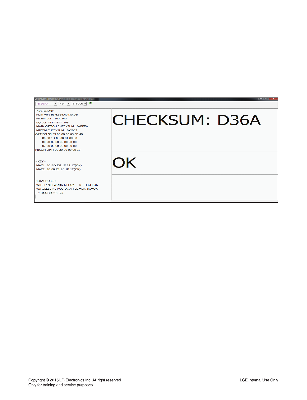
VERSION CHECK
1) PC IP setting
IP: 192.168.0.1
Subnet: 255.255.254.0
Gateway: 10.168.0.1
2) Open MP tool.
3) Set power on.
4) Press “ADD” button after connect LAN cable.
5) Display the version in the tool.
1-15
Page 17
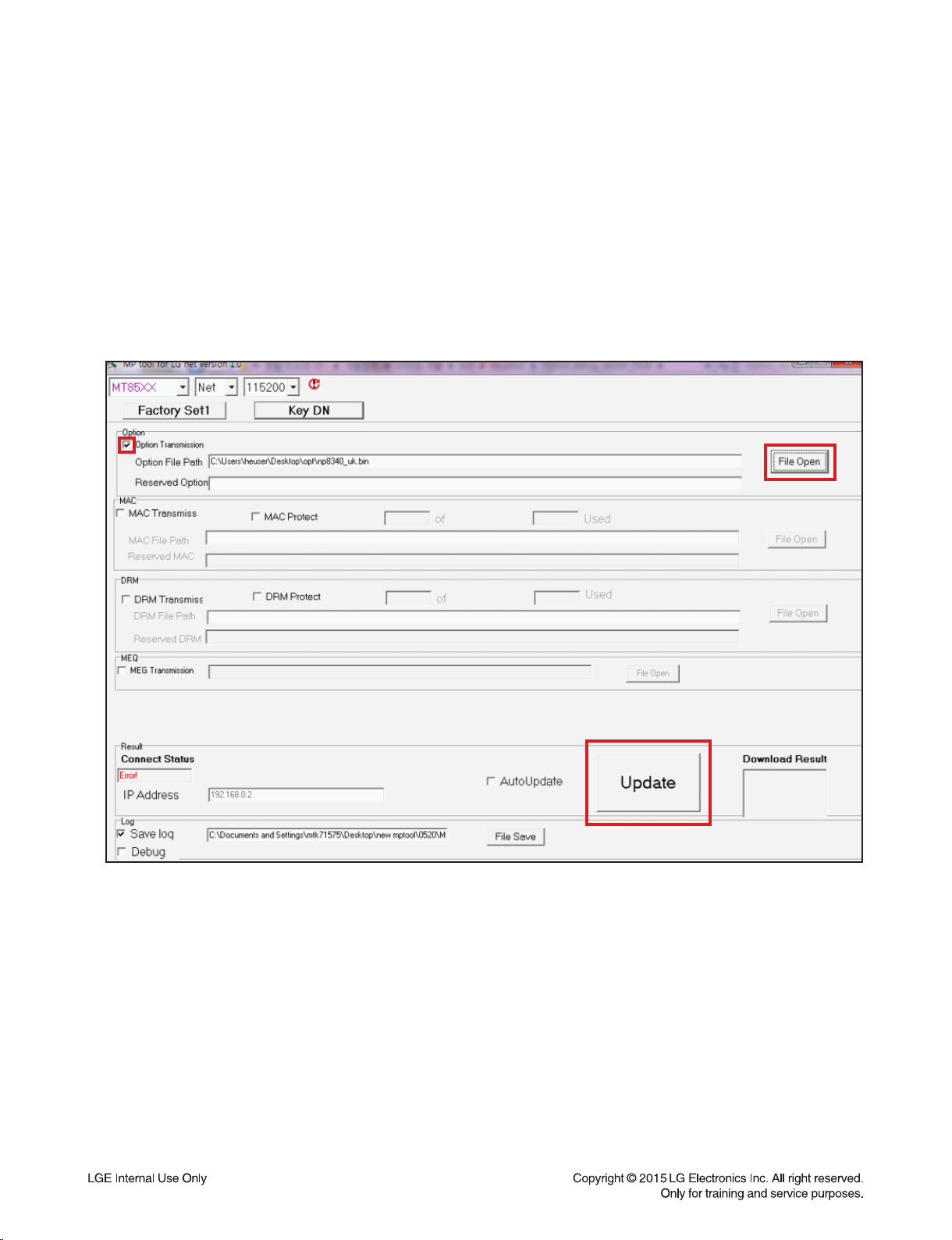
OPTION EDIT GUIDE
1-1. Option Edit-1
1) PC IP setting
IP: 192.168.0.1
Subnet: 255.255.254.0
Gateway: 10.168.0.1
2) Open MP tool.
3) Check Option Transmission and select option fi le by “File open” button.
4) Set power on.
5) Press “ADD” button after connect LAN cable.
6) Enter “Update” button in the tool menu.
7) Download result is “OK” or “NG”.
1-2. Option Edit-2 (Need a HTS Remote control)
1) Hidden mode : Remote control “2” + “Vol-” key
2) Change option code by remote control.
1-16
Page 18

SPECIFICATIONS
• GENERAL
Power requirements Refer to the main label on the unit.
Power consumption 50 W
Networked standby : 6.0 W (If all network ports are activated.)
Dimensions (W x H x D) (1100 x 106 x 135) mm (without Foot)
Net Weight (Approx.) 8.2 kg
Operating temperature 5 °C to 35 °C
Operating humidity 5 % to 90 %
• INPUT/OUTPUT
OPT. IN 3 V (p-p), Optical jack x 2
PORTABLE IN 0.5 Vrms (3.5 mm stereo jack) x 1
HDMI IN 19 Pin (Type A, HDMI™ connector) x 3
HDMI OUT 19 Pin (Type A, HDMI™ connector) x 1
Available Digital Input
Audio Sampling Frequency 32 kHz, 44.1 kHz, 48 kHz, 96 kHz
• AMPLIFIER
Total 700 W
Front 75 W x 2 (4 Ω at 1 kHz)
Rear 75 W x 2 (4 Ω at 1 kHz)
Surround 75 W x 2 (4 Ω at 1 kHz)
Center 75 W (4 Ω at 1 kHz)
Subwoofer 175 W (3 Ω at 80 Hz)
THD 10 %
• WIRELESS SUBWOOFER
Power requirements Refer to the main label on the subwoofer.
Power consumption 35 W
Type 1 Way 1 Speaker
Impedance 3 Ω
Rated Input Power 175 W
Max. Input Power 350 W
Dimensions (W x H x D) (296 x 332 x 296) mm
Net Weight (Approx.) 7.6 kg
• SYSTEM
ETHERNET (LAN) port Ethernet jack x 1, 10 BASE-T/100 BASE-TX
Wireless LAN (Internal antenna) Integrated IEEE 802.11n (Draft 2.0) wireless networking access,
compatible with 802.11a/b/g/n Wi-Fi networks.
• BLUETOOTH
Version 4.0
Codec SBC
• Designs and specifications are subject to change without prior notice.
1-17
Page 19

1-18
Page 20

SECTION 2
ELECTRICAL
CONTENTS
ONE POINT REPAIR GUIDE ............................................................................................................................ 2-2
1. NO POWER PROBLEM. ........................................................................................................................ 2-2
2. NO BOOTING WHEN YOU TURN THE UNIT ON, NO MESSAGE OR
“HELLO” ON FRONT PANEL ................................................................................................................. 2-4
3. NO SOUND ............................................................................................................................................. 2-7
ELECTRICAL TROUBLESHOOTING GUIDE ................................................................................................. 2-12
1. POWER SUPPLY ON SMPS BOARD .................................................................................................. 2-12
2. POWER SUPPLY ON MAIN BOARD ................................................................................................... 2-13
3. SYSTEM PART ..................................................................................................................................... 2-19
4. NO AUDIO OUTPUT ............................................................................................................................ 2-21
5. NO HDMI OUTPUT ............................................................................................................................... 2-23
WAVEFORMS OF MAJOR CHECK POINT .................................................................................................... 2-24
1. ADC I2S WAVEFORM (IC200) ............................................................................................................. 2-24
2. DSP OUTPUT I2S WAVEFORM (IC600) ............................................................................................. 2-25
3. LCD DATA LINE OUTPUT WAVEFORM (IC100) ................................................................................ 2-26
4. RMC WAVEFORM ................................................................................................................................ 2-27
5. I2C WAVEFORM .................................................................................................................................. 2-28
WIRING DIAGRAM .......................................................................................................................................... 2-31
BLOCK DIAGRAMS ........................................................................................................................................ 2-33
1. POWER BLOCK DIAGRAM ................................................................................................................. 2-33
2. SYSTEM BLOCK DIAGRAM ................................................................................................................ 2-35
CIRCUIT DIAGRAMS ...................................................................................................................................... 2-37
1. SMPS CIRCUIT DIAGRAM .................................................................................................................. 2-37
2. MAIN - MICOM CIRCUIT DIAGRAM .................................................................................................... 2-39
3. MAIN - MPEG CIRCUIT DIAGRAM ...................................................................................................... 2-41
4. MAIN - MEMORY CIRCUIT DIAGRAM ................................................................................................ 2-43
5. MAIN - ADC & I/O CIRCUIT DIAGRAM ............................................................................................... 2-45
6. MAIN - DCDC CIRCUIT DIAGRAM ...................................................................................................... 2-47
7. MAIN - DSP CIRCUIT DIAGRAM ......................................................................................................... 2-49
8. MAIN - DAC / AMP CIRCUIT DIAGRAM .............................................................................................. 2-51
9. HDMI CIRCUIT DIAGRAM.................................................................................................................... 2-53
10. FRONT CIRCUIT DIAGRAM ................................................................................................................ 2-55
11. KEY CIRCUIT DIAGRAM...................................................................................................................... 2-57
CIRCUIT VOLTAGE CHART ........................................................................................................................... 2-59
1. ICs ......................................................................................................................................................... 2-59
2. CAPACITORS ....................................................................................................................................... 2-61
3. CONNECTORS ..................................................................................................................................... 2-62
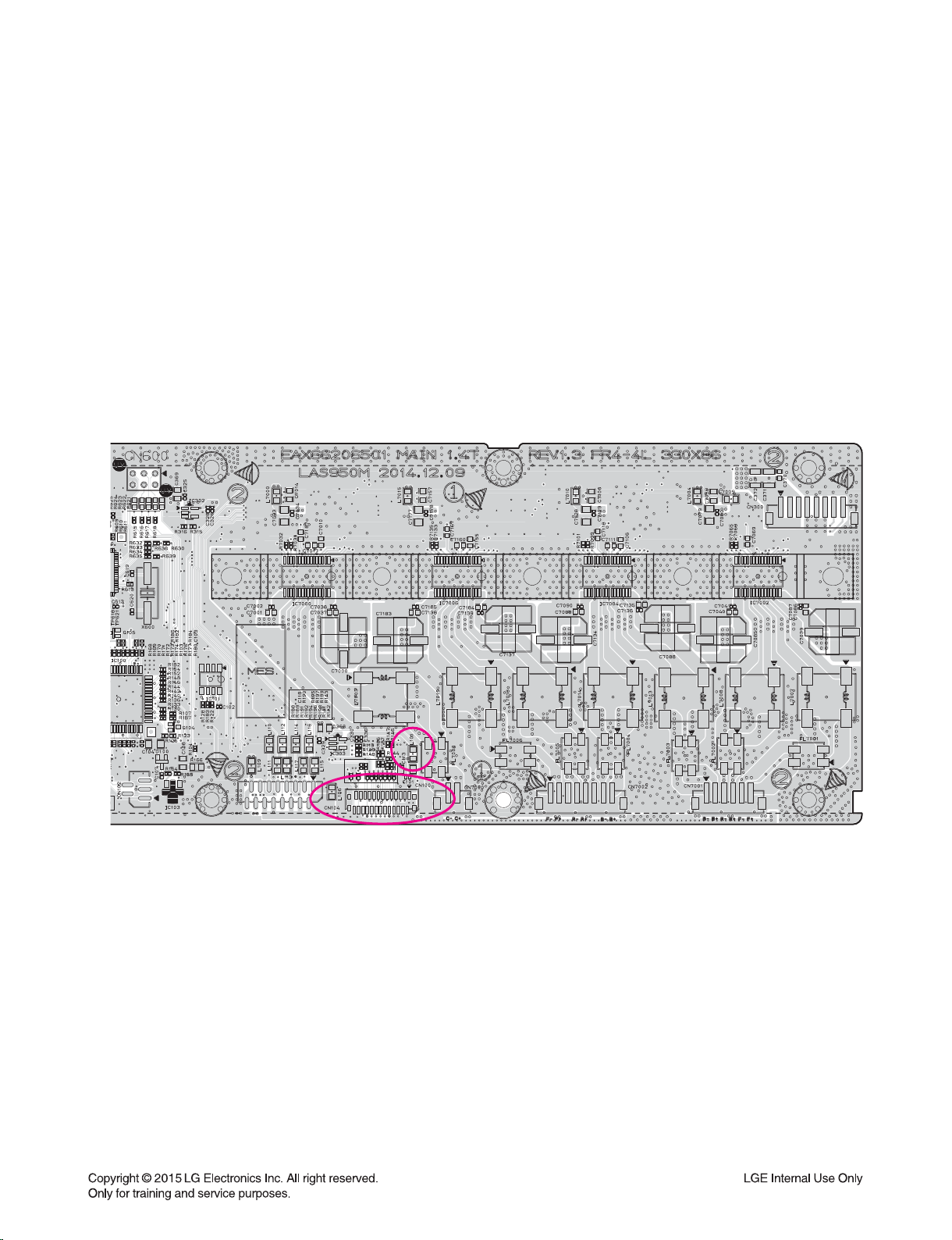
PRINTED CIRCUIT BOARD DIAGRAMS ....................................................................................................... 2-63
1. SMPS P. C. BOARD DIAGRAM ........................................................................................................... 2-63
2. MAIN P. C. BOARD DIAGRAM ............................................................................................................ 2-65
3. HDMI P. C. BOARD DIAGRAM ............................................................................................................ 2-67
4. FRONT P. C. BOARD DIAGRAM ......................................................................................................... 2-67
5. KEY P. C. BOARD DIAGRAM .............................................................................................................. 2-67
2-1
Page 21
ONE POINT REPAIR GUIDE
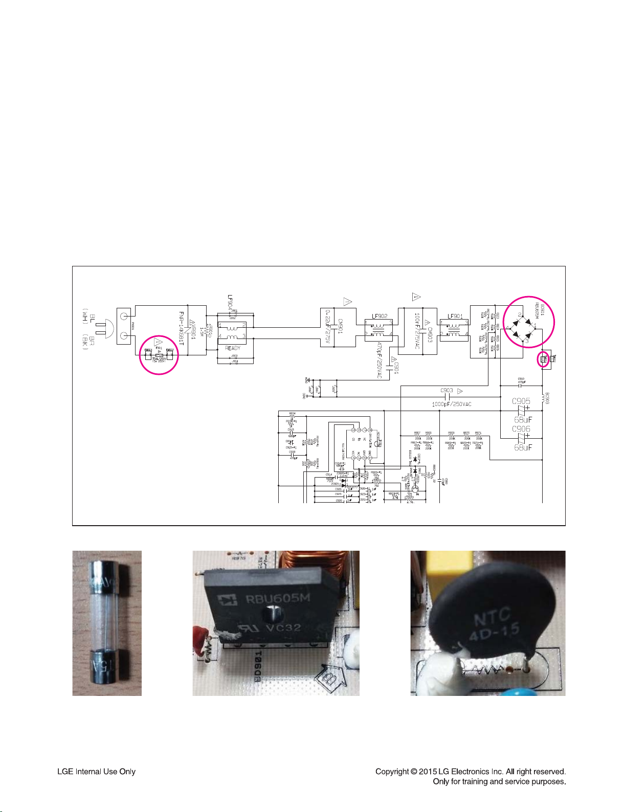
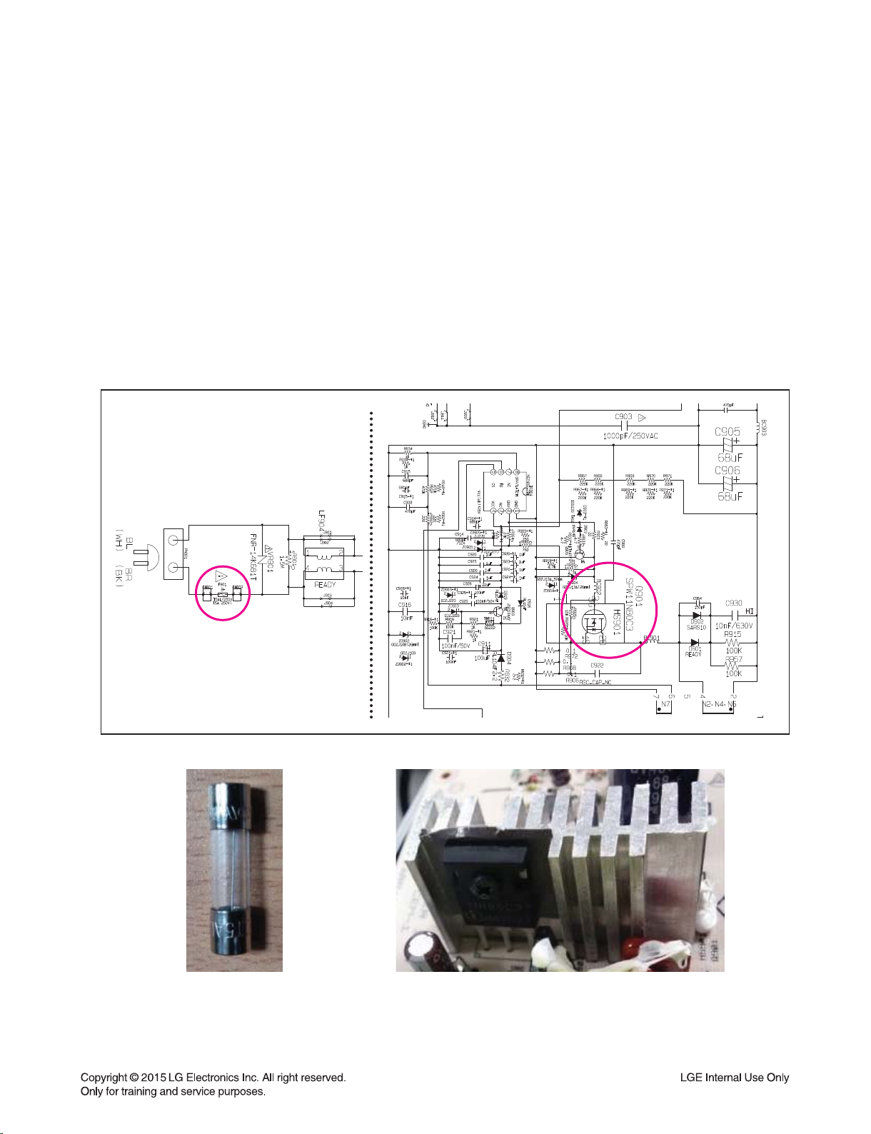
1. NO POWER PROBLEM
If the unit doesn’t work by no power problem, repair the set according to the following guide.
1-1. No power
1-1-1. Solution
Replace F901, BD901, TH901 on SMPS board.
1-1-2. How to troubleshoot (Countermeasure)
1) Check if the fuse F901 is open or short-circuit.
2) Check if the bridge diode BD901 is short-circuit by over current with a digital multimeter.
3) Check if the NTC thermistor TH901 is normal or open.
1-1-3. Service hint (Any picture / Remark)
F901
If F901 is not
short-circuit,
replace it with a
same specifi cations
one.
BD901
If BD901 is short-circuit,
replace it with a new one.
2-2
TH901
If TH901 is open,
replace it with a new one.
Page 22
ONE POINT REPAIR GUIDE
NO POWER PROBLEM
If the unit doesn’t work by no ±PVDD problem, repair the set according to the following guide.
1-2. No AMP power
1-2-1. Solution
Replace F901, Q901 on SMPS board.
1-2-2. How to troubleshoot (Countermeasure)
1) Check if the fuse F901 is open or short-circuit.
2) Check the Drain-Source or Drain-Gate, Gate-Source Resistance of Q901 with a digital multimeter.
If it is short condition, it’s destroyed. Replace it with a new one.
(Please replace FET at the same time although several FET is OK)
1-2-3. Service hint (Any picture / Remark)
If F901 is not short-circuit,
F901
replace it with a same specifi cations one.
Q901
If Q901 is short-circuit,
replace it with a new one.
2-3
Page 23
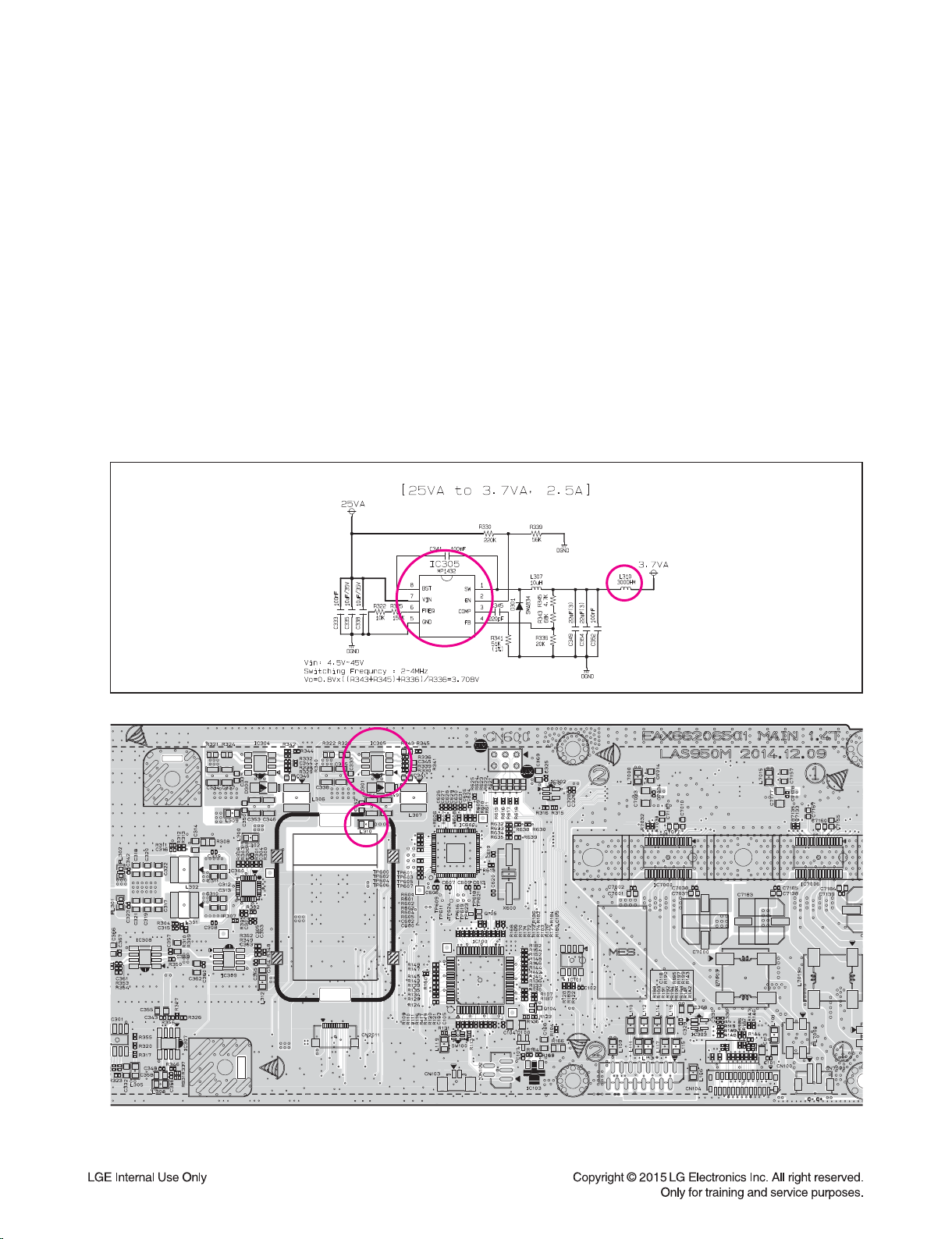
ONE POINT REPAIR GUIDE
IC305
L310
2. NO BOOTING WHEN YOU TURN THE UNIT ON, NO MESSAGE OR
“HELLO” ON FRONT PANEL
When you turn on your set, it will blank / no message on front panel, and stand-by LED
doesn't work.
2-1. IC305 System 3.7 VA (No 3.7 VA)
2-1-1. Solution
Replace IC305 on MAIN board.
2-1-2. How to troubleshoot (Countermeasure)
1) Please check 25 VA of IC305 pin7 (VIN).
2) If 25 VA is abnormal, please check SMPS board.
3) If 25 VA is OK, but 3.7 VA is abnormal at the IC305 pin1 (VOUT) & L310, replace IC305.
2-1-3. Service hint (Any picture / Remark)
L310
IC305
< MAIN board top view >
2-4
Page 24
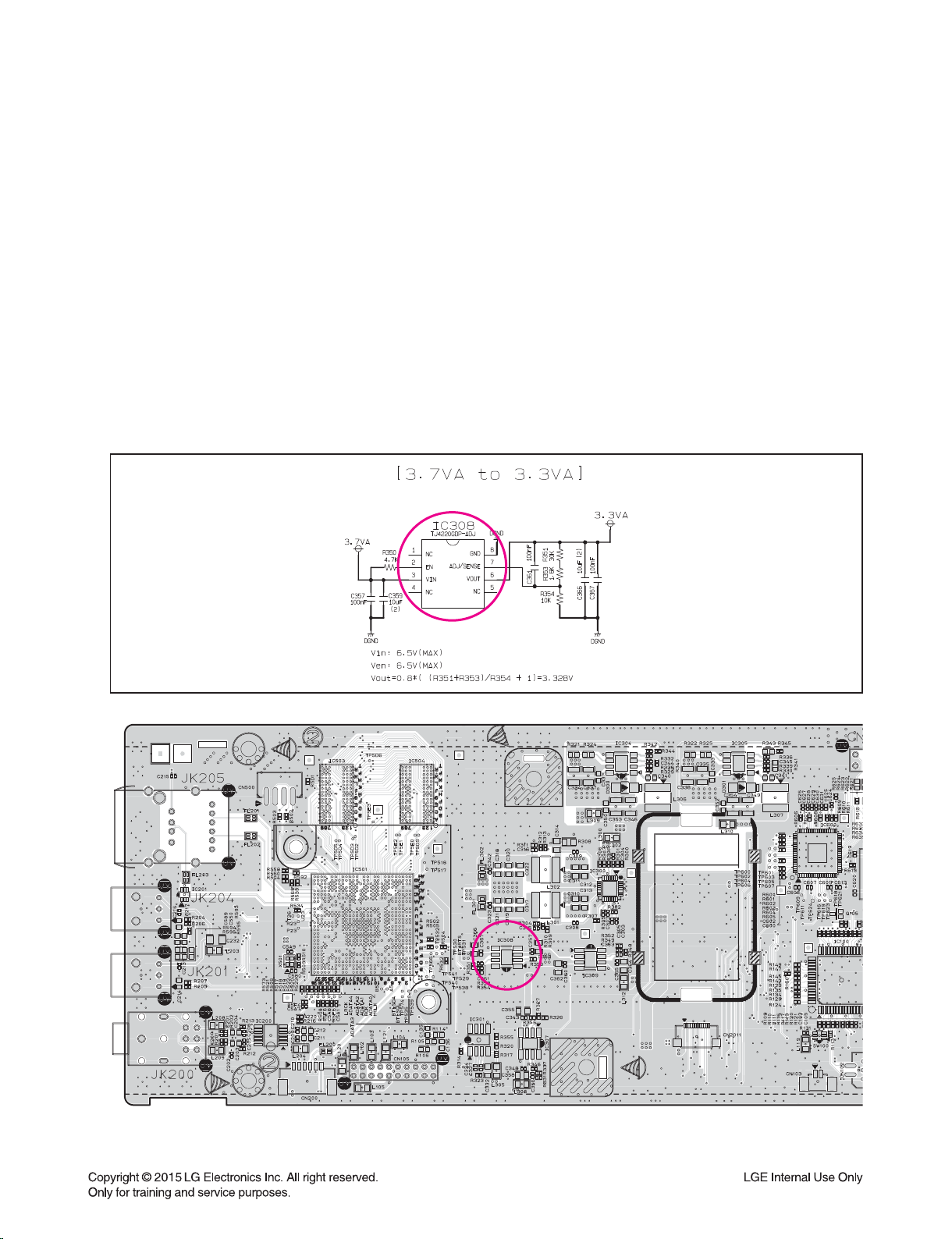
ONE POINT REPAIR GUIDE
IC308
NO BOOTING WHEN YOU TURN THE UNIT ON, NO MESSAGE OR
“HELLO” ON FRONT PANEL
When you turn on your set, it will blank / no message on front panel, and stand-by LED
doesn't work.
2-2. IC308 System 3.3 VA (No 3.3 VA)
2-2-1. Solution
Replace IC308 on MAIN board.
2-2-2. How to troubleshoot (Countermeasure)
1) Please check 3.7 VA of IC308 pin3 (VIN).
2) If 3.7 VA is abnormal, please check IC305 pin1 (VOUT).
3) If 3.7 VA is OK, but 3.3 VA is abnormal at the IC308 pin6 (VOUT), replace IC308.
2-2-3. Service hint (Any picture / Remark)
IC308
< MAIN board top view >
2-5
Page 25
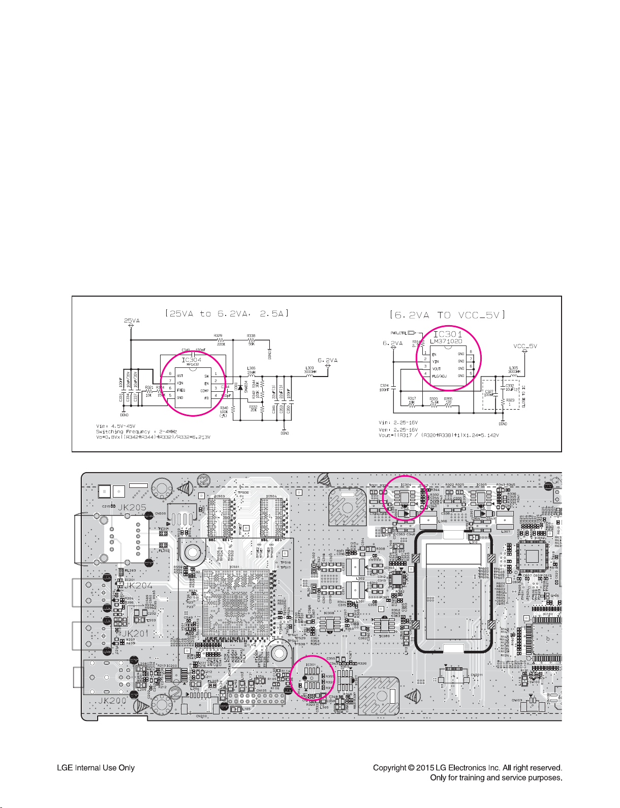
ONE POINT REPAIR GUIDE
IC304
IC301
NO BOOTING WHEN YOU TURN THE UNIT ON, NO MESSAGE OR
“HELLO” ON FRONT PANEL
When you turn on your set, it will blank / no message on front panel, and stand-by LED
doesn't work.
2-3. LCD System power 5 V, 6.2 VA (No VCC_5V, No 6.2VA)
2-3-1. Solution
Replace IC301, IC304 on MAIN board.
2-3-2. How to troubleshoot (Countermeasure)
1) Please check CN401 pin7 (VCC_5V), pin10 (6.2VA).
2) If 5 V, 6.2 VA is abnormal, please check IC301 pin3 (VOUT), IC304 pin1 (SW).
3) If 5 V, 6.2 VA is abnormal, replace IC301, IC304.
2-3-3. Service hint (Any picture / Remark)
IC301
< MAIN board top view >
2-6
IC304
Page 26
ONE POINT REPAIR GUIDE
CN100
L101
3. NO SOUND
3-1. WIRELESS
3-1-1. Solution
Replace IC102 on MAIN board.
3-1-2. How to troubleshoot (Countermeasure)
1) Please check externally status of Wireless module cable connection on your eyes.
(at CN100 and Wireless module)
2) Please check 3.3 V of WLS_3.3V (at L101).
If 3.3 V is OK, please check SPI signal (WL_SPI_CS/DO/WP/DI/CLK) of IC102 (pin1, 2, 3, 5, 6).
3) If you can’t have no signal, please replace IC102.
4) If 3) is ok, and proceed S/W update (Main set, Wireless Subwoofer) when set is paired.
3-1-3. Service hint (Any picture / Remark)
L101
CN100
< MAIN board top view >
2-7
Page 27
ONE POINT REPAIR GUIDE
CN2001
L205
NO SOUND
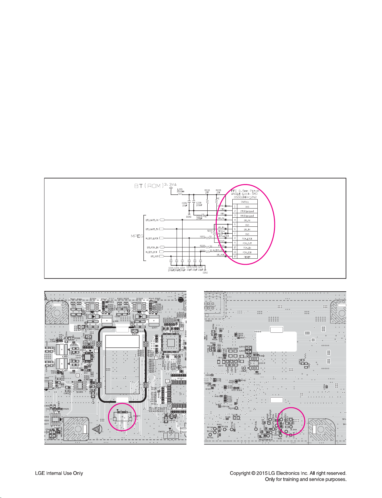
3-2. BLUETOOTH
3-2-1. Solution
Replace IC501 on MAIN board.
3-2-2. How to troubleshoot (Countermeasure)
1) Please check externally status of Bluetooth module cable connection on your eyes.
(at CN2011 and Bluetooth module)
2) Please check 3.3 VA (at L205).
If 3.3 VA is OK, please check BT_RST, M_I2S_BCK, BT_PCM_IN of CN2011 (pin12, 11, 10)
and BT_UART_RX, BT_UART_TX (pin4, 6).
If you have no signal, please replace IC501.
3-2-3. Service hint (Any picture / Remark)
CN2001
< MAIN board top view > < MAIN board bottom view >
2-8
L205
Page 28
ONE POINT REPAIR GUIDE
R204
L203
R205
IC501
NO SOUND
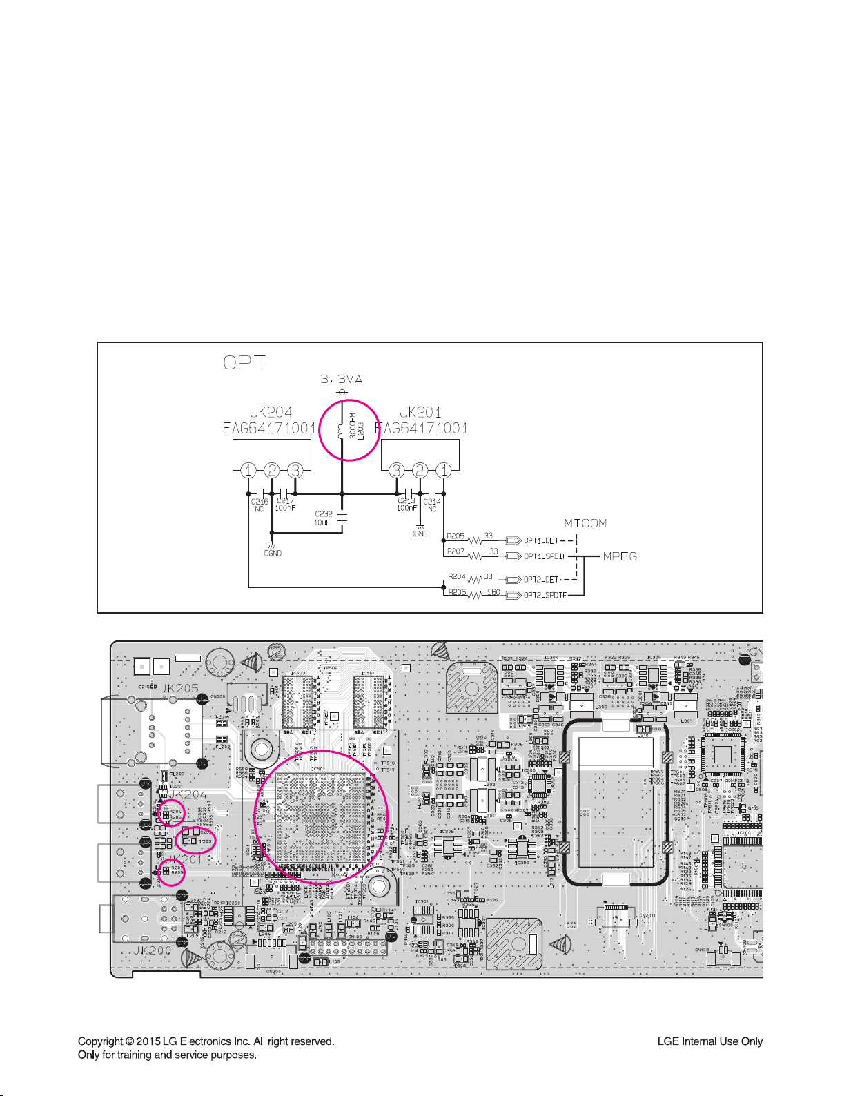
3-3. OPTICAL
3-3-1. Solution
Replace IC501 on MAIN board.
3-3-2. How to troubleshoot (Countermeasure)
1) Please check 3.3 VA (at L203).
2) If you can check 3.3 VA, please check OPT_DET signal (R204, R205) when optical mode.
3) In spite of process 2), set has abnormal output, then replace IC501.
3-3-3. Service hint (Any picture / Remark)
R204
L203
R205
IC501
< MAIN board top view >
2-9
Page 29

ONE POINT REPAIR GUIDE
CN803
CN802
CN800
CN801
IC803
IC801
IC800
IC802
NO SOUND
When unit is connected to HDMI TV using HDMI cable, picture shows bad color, no output or mixed
color on the screen. But component output is OK.
3-4. HDMI
3-4-1. Solution
Replace IC800, CN800, CN801, CN802, CN803 (HDMI jack).
3-4-2. How to troubleshoot (Countermeasure)
1) Check HDMI_5VA at pin3 of IC803.
2) Check HDMI_3.3V at pin3 of IC801.
3) Check HDMI_1V at pin8 of IC802.
4) 1), 2), 3) is OK
Replace IC800.
5) Check CN105, CN804 (MAIN HDMI B to B (board to board) connector).
6) B to B (board to board) connector is not good
Replace B to B (board to board) connector (CN105, CN804).
3-4-3. Service hint (Any picture / Remark)
CN803
CN800
IC801
IC800
IC802
IC803
< HDMI board top view >
2-10
CN802
CN801
Page 30

ONE POINT REPAIR GUIDE
IC7003
IC7005
IC7007
IC7001
IC802
NO SOUND
3-5. IC705 (DAC IC)
3-5-1. Solution
Replace IC7001, IC7003, IC7005, IC7007 (DAC IC).
3-5-2. How to troubleshoot (Countermeasure)
1) Check IC7001, IC7003, IC7005, IC7007 pin soldering.
2) If there is short soldering on pin, re-soldering.
3) Check DAC_3.3V at L7000, L7002, L7004, L7006, L7010, L7012, L7015, L7017.
4) If soldering is ok, replace IC7001, IC7003, IC7005, IC7007.
3-5-3. Service hint (Any picture / Remark)
IC802
IC7003
IC7005
IC7007
IC7001
< MAIN board bottom view >
2-11
Page 31

ELECTRICAL TROUBLESHOOTING GUIDE
1. POWER SUPPLY ON SMPS BOARD
Power on mode no output 25 VA.
Power off mode no output 12 VA.
YES
Is F901 normal?
YES
Is IC901 normal?
YES
Is the VCC
(10 ~ 28 V) supplied to IC901
pin4?
YES
Is Q901 normal?
NO
NO
NO
NO
Replace F901.
(same fuse)
Replace IC901.
Replace D903.
NO
Check or replace
D904.
YES
Replace Q903.
Replace Q901.
YES
Is PC901 normal?
YES
Is IC910 normal?
YES
Is D917 normal?
YES
Power line of MAIN board is short.
NO
NO
NO
2-12
Replace PC901.
Replace IC910.
Replace D917.
Page 32

ELECTRICAL TROUBLESHOOTING GUIDE
2. POWER SUPPLY ON MAIN BOARD
NO 3.7 VA
YES
Is 25 VA to pin7
of IC305 normal?
YES
Is D301 normal?
YES
Is switching pulse of
IC305 pin1 normal?
YES
3.7 VA power line is normal.
NO
NO
NO
Check 25 VA on SMPS board.
Replace D301.
Replace IC305.
NO 3.3 VA (MICOM)
YES
Is 3.7 VA to pin3
of IC308 normal?
YES
Is R350 & IC308 normal ?
YES
Are R351, R353, R354 normal ?
YES
3.3 VA power line is normal.
NO
NO
NO
2-13
Check IC305 & 3.7 VA power line.
Replace R350 & IC308.
Replace R351, R353, R354.
Page 33

ELECTRICAL TROUBLESHOOTING GUIDE
NO D_3.3V (DSP / MPEG)
YES
Is 3.7 VA to pin3
of IC309 normal?
YES
Is there DC voltage
to pin2 of IC309?
YES
Is there DC voltage
to pin6 of IC309?
YES
D_3.3V power line is normal.
NO
NO
NO
Check IC309 & 3.7 VA power line.
Check R347.
Check R348, R349, R352.
NO DAC_3.3V (DAC)
YES
Is 3.7 VA to pin1
of IC302 normal?
YES
Is there H (3.3 V) voltage
to pin3 of IC302?
YES
Is there DC voltage
to pin5 of IC302?
YES
DAC_3.3V power line is normal.
NO
NO
NO
2-14
Check IC305 & 3.7 VA power line.
Check R315.
Replace IC302.
Page 34

ELECTRICAL TROUBLESHOOTING GUIDE
NO WLS_3.3V (Wireless module)
YES
Is 3.7 VA to pin1
of IC303 normal?
YES
Is there H (3.3 V) voltage
to pin3 of IC303?
YES
Is there DC voltage
to pin5 of IC303?
YES
WLS_3.3V power line is normal.
NO
NO
NO
Check IC305 & 3.7 VA power line.
Check R318.
Replace IC303.
NO WIFI_3.5VA (Wi-Fi module)
YES
Is 3.7 VA to pin3
of IC307 normal?
YES
Is there H (3.3 V) voltage
to pin2 of IC307?
YES
Is there DC voltage
to pin6 of IC307?
YES
WIFI_3.5VA power line is normal.
NO
NO
NO
2-15
Check IC305 & 3.7 VA power line.
Check R327.
Replace IC307.
Page 35

ELECTRICAL TROUBLESHOOTING GUIDE
NO 6.2 VA
YES
Is 25 VA to pin7
of IC304 normal?
YES
Is D300 normal?
YES
Is switching pulse of
IC304 pin1 normal?
YES
6.2 VA power line is normal.
NO
NO
NO
Check 25 VA on SMPS board.
Replace D300.
Replace IC304.
NO VCC_5V (USB & LCD)
YES
Is 6.2 VA to pin2
of IC301 normal?
YES
Is there H (3.3 V) voltage
to pin1 of IC301?
YES
Is there DC voltage
to pin3 of IC301?
YES
VCC_5V power line is normal.
NO
NO
NO
2-16
Check IC304 & 6.2 VA power line.
Check R314.
Replace R317, R320, R355 & IC301.
Page 36

ELECTRICAL TROUBLESHOOTING GUIDE
NO 1.5 V (MPEG & DDR3)
YES
Is 6.2 VA to pin8, 13
of IC300 normal?
YES
Is there H (3.3 V) voltage
to pin6, 15 of IC300?
YES
Is switching pulse of
IC300 pin12 normal?
YES
1.5 V power line is normal.
NO
NO
NO
Check IC304 & 6.2 V power line.
Check R306, R307.
Replace IC300.
NO 1.2 V (MPEG CORE)
YES
Is 6.2 VA to pin8, 13
of IC300 normal?
YES
Is there H (3.3 V) voltage
to pin6, 15 of IC300?
YES
Is switching pulse of
IC300 pin9 normal?
YES
1.2 V power line is normal.
NO
NO
NO
2-17
Check IC304 & 6.2 V power line.
Check R306, R307.
Replace IC300.
Page 37

ELECTRICAL TROUBLESHOOTING GUIDE
NO HDMI_3.3V
YES
Is 3.7 VA to pin2 of
IC801 normal?
YES
Is there H (3.3 V) voltage
to pin1 of IC801?
YES
Is there DC voltage
to pin3 of IC801?
YES
HDMI_3.3V power line is normal.
NO
NO
NO
Check IC305 & 3.7 VA power line.
Check R848.
Replace R847, R849, R850 & IC801.
NO HDMI_1V
YES
Is HDMI_3.3V to pin1, 4
of IC802 normal?
YES
Is there DC voltage
to pin8 of IC802?
YES
HDMI_1V power line is normal.
NO
NO
2-18
Check IC801 & HDMI_3.3V power line.
Replace R852, R853 & IC802.
Page 38

ELECTRICAL TROUBLESHOOTING GUIDE
3. SYSTEM PART
POWER ON
STAND-BY LED OK ?
NO
3B
Pin1 of IC305
and pin6 of IC308
are OK?
Check MICOM
S/W download.
YES
NO
Check IC305, IC308
and SMPS board.
MAIN Board
3A
YES
3.3 VA OK?
YES
Check Q402, LD400.
MAIN to FRONT cable
connection OK?
NO
NO
Check IC305, IC308.
FRONT Board
Proper cable connect.
2-19
Page 39

ELECTRICAL TROUBLESHOOTING GUIDE
3A
“HELLO”
Display on LCD
OK?
YES
NO
Signal
EEPROM_CLK / DAT
OK?
Signal
MICOM_UART_TX
MICOM_UART_RX
OK?
6.2 VA,
VCC_5V, F_3.3VA
OK?
MAIN Board
Signal
LCD_DO / CLK / STB
OK?
YES
YES
YES
NO
NO
NO
NO
Replace IC101.
(EEPROM)
Replace IC100 or IC501.
Replace LCD.
3C
Check connection
& LCD module.
System part OK.
3C
YES
Signal
BL_CTL
OK?
YES
FRONT Board
Proper assemble
MAIN, FRONT and KEY
board OK?
YES
2-20
NO
NO
3C
Check Q403.
3C
Assemble properly.
3B
Page 40

ELECTRICAL TROUBLESHOOTING GUIDE
4. NO AUDIO OUTPUT
SPEAKER OUTPUT
YES
SOUND OK?
YES
Pin39, 40, 41, 44, 49, 52
of IC600 signal OK?
YES
Pin6, 7
of IC7001, IC7003, IC7005, IC7007
signal OK?
YES
Pin21, 23, 27, 29
of IC7000, IC7002, IC7004, IC7006
signal OK?
YES
Replace MAIN board.
NO
NO
NO
NO
Check CN7000, CN7001 CN7002 or replace.
Check IC600 (DSP) or replace.
Check each DAC IC or replace.
Check each AMP IC or replace.
BLUETOOTH FUNCTION
YES
CN2011 status
OK?
YES
CN2011 pin1
3.3 VA OK?
YES
CN2011 I2S
signal OK?
YES
Replace BT module.
NO
NO
NO
2-21
Replace CN2011.
Check L205 & 3.3 VA line.
Check BT I2S signal line.
Page 41

ELECTRICAL TROUBLESHOOTING GUIDE
OPTICAL FUNCTION
YES
JK201, JK204
status OK ?
YES
JK201, JK204 pin3
3.3 VA OK?
YES
OPT1/2_DET
OPT1/2_SPDIF signal
OK?
YES
Replace IC501.
NO
NO
NO
Replace JK201, JK204.
Check L203 & 3.3 VA line.
Check OPT_SPDIF & OPT_DET signal line.
Wi-Fi FUNCTION
YES
CN200
status OK?
YES
CN200 pin6
WIFI_ 3.5VA OK?
YES
Wi-Fi Connection is OK?
YES
Replace Wi-Fi module.
NO
NO
NO
2-22
Replace CN200.
Check WIFI_3.5VA line.
Check Wi-Fi cable connection.
Page 42

ELECTRICAL TROUBLESHOOTING GUIDE
5. NO HDMI OUTPUT
No HDMI Audio / Video output
YES
CN105, CN804
B to B connector OK?
YES
CN803 pin18 &
HDMI_5.5VA OK?
YES
CN803 pin19 HP_DET
about 2.0 ~ 5.3 V OK?
YES
IC800
1.0 V, 3.3 V OK?
YES
X800
27 MHz OK?
YES
NO
NO
NO
NO
NO
Replace B to B (board to board) connector.
Check D812 & HDMI_5.5VA line.
Check hot plug detect signal from TV.
Check IC801, IC802, IC803.
Check X800 or replace.
IC100
HDMI_SCL/SDA, PWR_CTRL, CEC
OK?
YES
Is there signal on TMDS?
YES
HDMI output OK.
NO
NO
2-23
Check IC100.
Check TMDS trace from IC800.
Page 43

WAVEFORMS OF MAJOR CHECK POINT
1. ADC I2S WAVEFORM (IC200)
M_I2S_MCLK Waveform (24.576 MHz) - PIN6
M_I2S_BCK Waveform (3.072 MHz) - PIN8
M_I2S_LRCK Waveform (48.00 MHz) - PIN7
M_ADC_DATA Waveform - PIN9
2-24
Page 44

2. DSP OUTPUT I2S WAVEFORM (IC600)
DSP_I2S_BCK Waveform (12.288 MHz) - PIN40
DSP_I2S_LRCK Waveform (192 KHz) - PIN39
DSP_I2S_FL_RL/C_FW/FR_RR/BL_BR Waveform
& Rising time - PIN44, 49, 52
DSP_I2S_FL_RL/C_FW/FR_RR/BL_BR Waveform
& Rising time - PIN44, 49, 52
2-25
Page 45

3. LCD DATA LINE OUTPUT WAVEFORM (IC100)
LCD_DO Waveform - PIN44
LCD_STB Waveform - PIN45
LCD_CLK Waveform - PIN46
2-26
Page 46

4. RMC WAVEFORM
RMC LEAD CODE TIMING (SPEC 4.5 ms)
RMC LEAD CODE TIMING (SPEC 4.5 ms)
RMC BIT CODE TIMING (SPEC 0.56 ms)
2-27
Page 47

5. I2C WAVEFORM
UART_TX (MICOM MPEG)
UART_RX (MICOM MPEG)
SPI_CLK (MICOM DSP)
SPI_DAT (MICOM DSP)
2-28
Page 48

I2C WAVEFORM
HDMI_SCL (MICOM HDMI)
HDMI_SDA (MICOM HDMI)
DSP_OUTPUT_BCK (DSP DAC x 4 / Wireless)
DSP_OUTPUT_LRCK (DSP DAC x 4 / Wireless)
2-29
Page 49

2-30
Page 50

2-322-31
WIRING DIAGRAM
SMPS
KEY FRONT
LCD Module
Ethernet
+ USB
OPT
PTB
MAIN
ㇵ⮨
FFC Harness
䚌
⮨
a
s
B to B
ROM version
Wi-Fi
Wireless TX
NFC
OPT
12P, 0.5mm
ST, Lock, SMD
6P, 1.25mm
ST, Lock, SMD
(6630V90141E)
(EAG61090207)
26P, 0.5mm
ST, Non_Lock, SMD
(6630X60142K)
IR
TX
HDMI HDMI
HDMIHDMI
HDMI
2P, 1.25mm
AG, No n_Lock ,SMD
(6630V901352)
2P, 1.25mm
ST, Lock, SMD
(EAG60989201)
8P, 2.0mm
ST, SMD
8P, 2.50mm
Board IN
Type
2P, 2mm
ST, Lock , SMD
(EAG63514501)
6P, 2mm
ST, Lock , SMD
(EAG63270201)
S
16P, 1mm
ST, Non_Lock, SMD
(6630XE00116)
10P, 1mm
AG, Lock, SMD
(EAG62611102)
20P, 2mm
ST, SOCKET, SMD
(EAG63717506)
20P, 2mm
DIP HEADER, SMD
Download Connector
MTK Download 殯
4P, 2mm, ST, Non_Lock , SMD
MICOM Download 殯
5P, 1mm, ST, Non Lock, SMD
DSP Download 殯
10P, 2.54mm, ST, MAIL, SMD
8P, 2mm
ST, Lock , SMD
(EAG41647503)
16P, 1mm
ST, Non_Lock, SMD
(6630XE00116)
(EAG63717505)
Bottom side
Top side
Page 51

2-342-33
FUSE
(F901)
BD901
T901
TRANS
م
+
م
م
م
(C905,C906)
NOISE FILTER
BLOCK
(CM901,R901,
CM903,VR901,
LF901,LF902)
PHOTO COUPLER
(PC901)
SNUBBER
BLOCK
(D902,C964,C930
R915,R957,BC901)
DRIVE & S/W BLOCK
(IC101, D104, R105,
R102, C108 , C109,
ZD101,ZD102,C113)
Y-CAP
C903
Y-CAP
C901
RECTIFIER &
SMOOTING BLOCK
(D917,C951,
C952,C953)
25 VA (ON)
V-CTRL
OPT (Not Used)
12 VA (STAND-BY)
TH901
FEED-BACK
BLOCK
(R931,R920,R949
R930,R928.R914
C919.R907,R912
Q904, IC910)
BLOCK DIAGRAMS
1. POWER BLOCK DIAGRAM
Page 52

2-362-35
BT_RST/I2S/UART
ADC
PCM1808
Slave
OPTICAL IN1
D+/D -
M_BCK/LRCK/DATA0,1,2,3
DAC_RST/SPI_CLK/DI/DO/CS
LCD
KEY
DDR x 2
128 MB x 2
A_RA[0-14]
A_DQ[0-31]
SPI0
PORTABLE
USB(SVC)
DSP_MCLK/BCLK/LRCK
/CEN/FL/FR/REAR
TACT
MTK_RST/TX/RX/PWR_STATUS/INST_BOOT
TX
WOOFER
WL_RST/DAT/CLK/MUTE/INT/MSG_RDY
MICOM
RENESAS 64P
AZ7027
P_SENSE
WiFi_P/N
Wi-Fi
(NEW)
OPT1_DET
BT_RST/RX
EPHY_TDP/N, EPHY_RDP/N
ETHERNET
(ROM)
OPT1_SPDIF
ADC_MCLK/LRCK/BCK/M_ADC_DAT
EEPROM
(2 KB)
EEP_CLK/DAT
a
MT8506
1.2 / 1.5 / 3.3 V
DD/DTS Decoding
PTB_DET
AMP_PDN/SD/CLIP/MUTE
HDMI IN1
EDID_I2C/CEC/EDID_SW/HPD_MICOM
HDMI OUT
M_I2S_DATA2/LRCK/BCK
Flash
1 MB
SPI_DI/DO/CS/CLK/WP
LCD_DO/CLK
/STB/BL_CTRL
/RMC
TPA3116D2
TPA3116D2
TPA3116D2
TPA3116D2
LAS950M 525W (75 W * 7EA)
FRONT
Wireless Woofer
27 MHz
OPTICAL IN2
OPT2_SPDIF
OPT2_DET
NAND
512 MB
HDMI
Sil9533
TMDS/HPD/EDID_I2C/ARC/CEC
TMDS1/RX_HPD1/EDID_I2C/PWR5V_1
HDMI IN2
HDMI IN3
TMDS2/RX_HPD2/EDID_I2C/PWR5V_2
TMDS3/RX_HPD3/EDID_I2C/PWR5V_3
HDMI_RST/I2C/INT
HDMI_SPDIF
PCM5101
PCM5101
PCM5101
PCM5101
DAC_MUTE
27 MHz
Flash
1 MB
SPI_DI/DO/CS/CLK
12.288 MHz
//C
DSP
ADAU1452
LAS950M 175 W
2. SYSTEM BLOCK DIAGRAM
Page 53

2-382-37
A
1
2
3
4
5
6
7
8
9
10
11
12
B C D E F G H I J K L M N O P Q R ST
No Power
BD901 is Defective
No Power
Q905 is Defective
No Power
Q901 is Defective
No Power
Q903 is Defective
No Power
D917, D918 are Defective
Switching Error
IC901 is Defective
Switching Error
PC901 is Defective
Voltage Error
Q902 is Defective
Voltage Error
Q904 is Defective
No Power
F901 is Defective
SMPS
EAX66106001 Rev1.8(20)
2014.12.10
Warning
Parts that are shaded are critical with
respect to risk of fire or electrical shock.
CIRCUIT DIAGRAMS
1. SMPS CIRCUIT DIAGRAM
WHEN SERVICING THIS CHASSIS, UNDER NO
CIRCUMSTANCES SHOULD THE ORIGINAL
DESIGN BE MODIFIED OR ALTERED WITHOUT
PERMISSION FROM THE LG CORPORATION. ALL
COMPONENTS SHOULD BE REPLACED ONLY WITH
TYPES IDENTICAL TO THOSE IN THE ORIGINAL
CIRCUIT. SPECIAL COMPONENTS ARE SHADED
ON THE SCHEMATIC FOR EASY IDENTIFICATION.
THIS CIRCUIT DIAGRAM MAY OCCASIONALLY
DIFFER FROM THE ACTUAL CIRCUIT USED. THIS
WAY, IMPLEMENTATION OF THE LATEST SAFETY
AND PERFORMANCE IMPROVEMENT CHANGES
INTO THE SET IS NOT DELAYED UNTIL THE NEW
SERVICE LITERATURE IS PRINTED.
1. Shaded( ) parts are critical for safety. Replace only
with specified part number.
2. Voltages are DC-measured with a digital voltmeter
during Play mode.
IMPORTANT SAFETY NOTE :
Page 54

2-402-39
A
1
2
3
4
5
6
7
8
9
10
11
12
B C D E F G H I J K L M N O P Q R ST
MICOM
EAX66206501 Rev1.3(11) MAIN(#1)
2014.12.10
2. MAIN - MICOM CIRCUIT DIAGRAM
Page 55

2-422-41
A
1
2
3
4
5
6
7
8
9
10
11
12
B C D E F G H I J K L M N O P Q R ST
MPEG
EAX66206501 Rev1.3(11) MAIN(#2)
2014.12.10
3. MAIN - MPEG CIRCUIT DIAGRAM
Page 56

2-442-43
A
1
2
3
4
5
6
7
8
9
10
11
12
B C D E F G H I J K L M N O P Q R ST
MEMORY
EAX66206501 Rev1.3(11) MAIN(#3)
2014.12.10
4. MAIN - MEMORY CIRCUIT DIAGRAM
Page 57

2-462-45
A
1
2
3
4
5
6
7
8
9
10
11
12
B C D E F G H I J K L M N O P Q R ST
ADC & I/O
EAX66206501 Rev1.3(11) MAIN(#4)
2014.12.10
5. MAIN - ADC & I/O CIRCUIT DIAGRAM
Page 58

2-482-47
A
1
2
3
4
5
6
7
8
9
10
11
12
B C D E F G H I J K L M N O P Q R ST
DCDC
EAX66206501 Rev1.3(11) MAIN(#5)
2014.12.10
6. MAIN - DCDC CIRCUIT DIAGRAM
Page 59

2-502-49
A
1
2
3
4
5
6
7
8
9
10
11
12
B C D E F G H I J K L M N O P Q R ST
DSP
EAX66206501 Rev1.3(11) MAIN(#6)
2014.12.10
7. MAIN - DSP CIRCUIT DIAGRAM
Page 60

2-522-51
A
1
2
3
4
5
6
7
8
9
10
11
12
B C D E F G H I J K L M N O P Q R ST
DAC/AMP
EAX66206501 Rev1.3(11) MAIN(#7)
2014.12.10
8. MAIN - DAC / AMP CIRCUIT DIAGRAM
Page 61

2-542-53
A
1
2
3
4
5
6
7
8
9
10
11
12
B C D E F G H I J K L M N O P Q R ST
HDMI
EAX66166301 Rev1.3(11)
2014.12.10
9. HDMI CIRCUIT DIAGRAM
Page 62

2-562-55
A
1
2
3
4
5
6
7
8
9
10
11
12
B C D E F G H I J K L M N O P Q R ST
FRONT
EAX66225701 Rev1.3(11)
2014.12.10
10. FRONT CIRCUIT DIAGRAM
Page 63

2-582-57
A
1
2
3
4
5
6
7
8
9
10
11
12
B C D E F G H I J K L M N O P Q R ST
KEY
EAX66166401 Rev1.3(11)
2014.12.10
11. KEY CIRCUIT DIAGRAM
Page 64

2-602-59
CIRCUIT VOLTAGE CHART
1. ICs
Designator Desc. Voltage Spec Pin
Mearsured
Voltage
Main Board
IC100 MICOM VDD : 1.6 ~ 5.5V 15,16 3.28
IC101 EEPROM VCC : 1.8V ~ 5.5V 8 3.28
IC102 Serial Flash VCC : -0.5V ~ 4.6V 8 3.59
IC103 Voltage Detector VCC: Max 18V 1 3.64
IC200 A/D Converter
VCC: 4.5V~5.5V 3 5.08
VDD: 2.7V~3.6V 4 3.29
IC300 DCDC
Vin1: 4.5V~18V 8 6.15
Vin2: 4.5V~18V 13 6.15
IC301 LDO Vin : 2.25V ~ 16V 2 6.18
IC302 LDO Vout : 3.251V ~ 3.35V 5 3.27
IC303 LDO Vout : 3.251V ~ 3.35V 5 3.6
IC304 DCDC
Vin : 4.5V ~ 48V 7 25.4
Vout : 0.8V ~ 42V 1 6.24
IC305 DCDC
Vin : 4.5V ~ 48V 7 25.4
Vout : 0.8V ~ 42V 1 3.75
IC307 LDO
Vin: 2.5V~5.5V 3 3.67
Vout:0.8V~5V 6 3.49
IC308 LDO
Vin: 2.5V~5.5V 3 3.67
Vout:0.8V~5V 6 3.27
IC309 LDO
Vin: 2.5V~5.5V 3 3.67
Vout:0.8V~5V 6 3.3
IC501 MPEG
DVCC12: 1.14V~1.26V K12 1.19
DVCC33: 3.15V~3.45V G14 3.367
AVDD12: 1.14V~1.26V N23 1.19
AVDD33: 3.15V~3.45V R26 3.367
DDRVCCIO1: 1.425V~1.575V AC3 1.552
DDRVREF: 0.775V N8 0.775
IC503 DDR
VDD : 1.425 ~ 1.575 B2,D9,G7,K2,K8,N1,N9,R1,R9 1.552
VREFCA: 0.49*VDD~0.51*VDD M8,H1 0.775
VDDQ:+1.425V~+1.575V A1,A8,C1,C9,D2,E9,E1,H2,H9 1.552
IC504 DDR
VDD : 1.425 ~ 1.575 B2,D9,G7,K2,K8,N1,N9,R1,R9 1.552
VREFCA: 0.49*VDD~0.51*VDD M8,H1 0.775
VDDQ:+1.425V~+1.575V A1,A8,C1,C9,D2,E9,E1,H2,H9 1.552
IC505 NAND VCC : 2.7V ~ 3.6V 12,37 3.366
IC600
AVDD : 1.2V ~ 3.3V 2,7,15,18,38,56 3.29
DVDD : 1.14V ~ 1.26V 20,35,53,71 1.104
IC601 Serial Flash VCC : -0.5V ~ 4.6V 8 3.29
IC7000 PVCC : -0.3V ~ 30V 17,18,19,31,32 25.4
IC7001 D/A Converter VDD : -0.3 ~ 20V 8,20 3.27
IC7002 PVCC : -0.3V ~ 30V 17,18,19,31,32 25.4
IC7003 D/A Converter VDD : -0.3 ~ 20V 8,20 3.27
IC7004 PVCC : -0.3V ~ 30V 17,18,19,31,32 25.4
IC7005 D/A Converter VDD : -0.3 ~ 20V 8,20 3.27
IC7006 PVCC : -0.3V ~ 30V 17,18,19,31,32 25.4
IC7007 D/A Converter VDD : -0.3 ~ 20V 8,20 3.27
Designator Desc. Voltage Spec Pin
Mearsured
Voltage
HDMI Board
IC800 HDMI
AVDD33 : 3.14V ~ 3.46V 14,33 3.33
IOVCC33 : 3.14V ~ 3.46V 63,88 3.29
SBVCC5V : 4.5V ~ 5.5V 45 5
AVDD10 : 0.95V ~ 1.05V 12,14,62,67,72,77 0.995
IC801 LDO Vin : 2.25V ~ 16V 2 6.17
IC802 LDO Vin : 2.5V ~ 6V 1 3.33
IC803 LDO Vin : 2.25V ~ 16V 2 3.66
Page 65

2-622-61
Location Value Capacitor (uF) Voltage Spec
100V-10% 240V/50Hz+10%
Measured voltage Measured voltage
SMPS Board
C905 68uF 460V 154.5V 310V
C906 68uF 460V 154.5V 310V
C911 100uF 50V 25.9V 26V
C919 1uF 50V 20.9V 20.9V
C928 1uF 50V 20.2V 20.3V
C951 1000uF 35V 25.9V 25.9V
C952 1000uF 35V 25.9V 25.9V
C953 1000uF 35V 25.9V 25.9V
Part Designator Voltage Spec Pin
Mearsured Voltage
#79 / #1
Remarks
MAIN
CN100 WLS_3V3 1 3.62 Wireless
CN104
VCC_5V 13 5.08
FRONT6.2VA 14 6.17
3.7VA 15,16 3.67
CN105
6.2VA 1 6.18
HDMI
3.7VA 2 3.67
VCC_5V 5 5.07
D_3.3V 8 3.29
CN200 WIFI_3.5VA 6 3.67 WIFI
CN300 25VA 1,2,3 25.3 SMPS
CN2011 3.3VA 1 3.28 BT
HDMI CN804
6.2VA 1 6.18
MAIN
3.7VA 2 3.67
VCC_5V 5 5.07
D_3.3V 8 3.29
FRONT
CN400
VCC_5V 13 5.08
MAIN6.2VA 14 6.17
3.7VA 15,16 3.66
CN401
F_3.3VA 4,6 3.44
LCDVCC_5V 7 5.07
6.2VA 10 5.78
2. CAPACITORS 3. CONNECTORS
Designator Voltage Spec Mearsured Voltage
Main & AMP Board
C7000 25V 25.4
C7039 25V 25.4
C7085 25V 25.4
C7088 25V 25.4
C7134 25V 25.4
C7137 25V 25.4
C7183 25V 25.4
Page 66

2-642-63
PRINTED CIRCUIT BOARD DIAGRAMS
1. SMPS P. C. BOARD DIAGRAM
(TOP VIEW)
(BOTTOM VIEW)
NOTE) Warning
Parts that are critical with respect to risk
of fire or electrical shock.
Page 67

2-662-65
2. MAIN P. C. BOARD DIAGRAM
(TOP VIEW)
(BOTTOM VIEW)
Page 68

2-682-67
3. HDMI P. C. BOARD DIAGRAM
4. FRONT P. C. BOARD DIAGRAM
5. KEY P. C. BOARD DIAGRAM
(TOP VIEW)
(TOP VIEW)
(TOP VIEW)
(BOTTOM VIEW)
(BOTTOM VIEW)
(BOTTOM VIEW)
Page 69

2-702-69
Page 70

SECTION 3
CABINET & MAIN CHASSIS
CONTENTS
DISASSEMBLY INSTRUCTIONS ................................................................................................................... 3-3
EXPLODED VIEWS ......................................................................................................................................... 3-9
1. MAIN SET SECTION ................................................................................................................................ 3-9
2. WIRELESS SUBWOOFER SECTION .................................................................................................... 3-11
3. PACKING ACCESSORY SECTION ....................................................................................................... 3-13
3-1
Page 71

DISASSEMBLY INSTRUCTIONS
Before you begin, position the main set upside down.
1. Cover Bottom Assembly
1) Remove the 20 screws on the main set.
2) Remove the Cover Bottom Assembly.
Cover Bottom Assembly
2
1
2. Cover Back
1) Remove the 11 screws securing the Cover Back.
2) Detach the power cord from the Cover Back.
3) Remove the Cover Back.
1
Fig. 1
2
3
Cover Back
1
1
Fig. 2
3-2
Power Cord
Page 72

3. Chassis Main Assembly
KEY
MAIN
1) Remove the 10 (②) screws securing the Chassis Main Assembly.
2) Disconnect the Harness/FFC cables from the Main Board.
3) Remove the Chassis Main Assembly.
3 Chassis Main Assembly
2
MAIN
MAIN
2
1
1
4. Key Board
1) Remove the 2 screws securing the Button Assembly.
2) Remove the Button Assembly (Bracket Button + Button).
3) Disconnect the Harness cable from the Key Board.
4) Remove the 2 screws securing the Key Board.
5) Remove the Key Board.
1
2
KEY
4
KEY
3
Button
Bracket Button
Fig. 3
Fig. 4
3-3
Page 73

5. SMPS Board
MAIN
HDMI
Chassis Cover
SMPS
1) Disconnect the Harness cable from the Main Board.
2) Remove the 4 (①) screws securing the SMPS Board.
3) Remove the SMPS Board.
6. Bluetooth Module
1) Disconnect the FFC cable from the Main Board.
2) Remove the Bracket BT.
3) Remove the Bluetooth Module.
1
2
MAIN
3
1
Bluetooth Module
2
3
Fig. 5
6. HDMI & Main Board
1) Remove the 4 screws securing the Chassis Cover.
2) Remove the Chassis Cover.
3) Remove the 5 screws securing the HDMI jack and the Chassis jack.
4) Remove the HDMI Board and the Chassis jack.
5) Remove the 2 (①) screws securing the Main Board.
6) Remove the Main Board.
1
1
2
Chassis Cover
Chassis Cover
3
3
3
3
SMPS
SMPS
2
MAIN
MAIN
6
5
HDMI
HDMI
4
Chassis jack
Fig. 6
3-4
Page 74

7. Cover Top Assembly
1) Remove the 10 screws securing the Cover Top Assembly.
2) Remove the Cover Top Assembly.
1
Cover Top Assembly
2
[Reassembly CAUTION]
Fig. 7
3-5
Page 75

8. Wi-Fi Module
1) Remove the 2 screws securing the Bracket Wi-Fi.
2) Disconnect the Harness cable from the Wi-Fi Module.
3) Remove the Wi-Fi Module.
9. Wireless Module
1) Remove the 2 screws securing the Wireless Module.
2) Disconnect the FFC cable from the Wireless Module.
3) Remove the Wireless Module.
10. Case Chamber Assembly
1) Remove the 6 screws securing the Case Chamber Assembly.
2) Remove the Case Chamber Assembly.
1
1
Wi-Fi Module
2
Case Chamber Assembly
1
2
2
1
Wireless Module
Fig. 8
3-6
Page 76

11. Case Back Center
FRONT
1) Remove the 8 screws securing the Case Back Center.
2) Detach the EMI Gasket.
3) Remove the Case Back Center.
1
3
2
12. Front Board
1) Remove the 4 screws securing the Front Board.
2) Remove the Front Board.
1
FRONT
FRONT
Fig. 9
1
2
Fig. 10
3-7
Page 77

3-8
Page 78

Wi-Fi
BT
K
J
K
I
251
A51
250
A52
CABLE2
CABLE1
D
E
C
274L
274C
274R
SPK7001
SPK7000
SPK7002
272
273
273
273
272
506
270
271
A42
A
300
A44
SMPS
A
B
A47
HDMI
A48
MAIN
C
D
E
F
G
H
I
J
B
A46
M
A43
KEY
L
A55
H
L
M
G
255
464
320
464
464
470
470
254
464
464
470
253
252
250
470
330
331
464
263
261
464
465
280
282
281L
256
470
282
281R
464
464
A41
464
260
464
464
464
464
WIRELESS
F
A54
CABLE4
CABLE3
CABLE5
464
464
464
464
464
331
262
EXPLODED VIEWS
1. MAIN SET SECTION
NOTES) THE EXCLAMATION POINT WITHIN AN
EQUILATERAL TRIANGLE IS INTENDED
TO ALERT THE SERVICE PERSONNEL
TO THE PRESENCE OF IMPORTANT
SAFETY INFORMATION IN SERVICE
LITERATURE.
Page 79

F
E
B
C
D
A
E
C
A
B
D
F
A81M
A331
A332
A330
A81A
A81S
A81L
A81K
381
382
383
391
392
393
393
392
392
389
384
393
385
387
395
390
388
388
395
386
WIRELESS
LED
KEY
AMP
SMPS
2. WIRELESS SUBWOOFER SECTION
NOTES) THE EXCLAMATION POINT WITHIN AN
EQUILATERAL TRIANGLE IS INTENDED
TO ALERT THE SERVICE PERSONNEL
TO THE PRESENCE OF IMPORTANT
SAFETY INFORMATION IN SERVICE
LITERATURE.
Page 80

3. PACKING ACCESSORY SECTION
831 LAN cable
801 Owner’s manual
806 Optical cable
829 Cable tie
836 Screws (2)
839 IR Blaster
803 Main packing
808 Batteries (2)
832 Music Flow Bundle S/W
835 Wall bracket
837 Cover foot (2)
900 Remote control
802 Box
804 Bag
Page 81

3-163-15
Page 82

SECTION 4
WIRELESS SUBWOOFER PART
CONTENTS
ONE POINT REPAIR GUIDE ............................................................................................................................ 4-2
1. NO POWER PROBLEM ......................................................................................................................... 4-2
2. POWER ON ERROR (12 V, 5 VA) ......................................................................................................... 4-4
3. POWER ON ERROR (3.3 VA, 3 V) ........................................................................................................ 4-5
4. WIRELESS CONNECTION .................................................................................................................... 4-6
CIRCUIT DIAGRAMS ........................................................................................................................................ 4-7
1. WOOFER SMPS CIRCUIT DIAGRAM ................................................................................................... 4-7
2. WOOFER AMP CIRCUIT DIAGRAM ...................................................................................................... 4-9
3. WOOFER KEY CIRCUIT DIAGRAM .................................................................................................... 4-11
PRINTED CIRCUIT BOARD DIAGRAMS ....................................................................................................... 4-13
1. WOOFER SMPS P. C. BOARD ............................................................................................................ 4-13
2. WOOFER AMP P. C. BOARD .............................................................................................................. 4-15
3. WOOFER KEY P. C. BOARD ............................................................................................................... 4-15
4-1
Page 83

ONE POINT REPAIR GUIDE
BD901
F901
1. NO POWER PROBLEM
No power problem occurs when you power on the unit.
1-1. Fuse & Bridge diode
1-1-1. Solution
Replace F901, BD901 on SMPS board.
1-1-2. How to troubleshoot (Countermeasure)
1) Look at the physical of fuse F901.
2) Check the bridge diode BD901.
1-1-3. Service hint (Any picture / Remark)
< Fuse, F901 >
Can look at physical condition.
4-2
BD901
< Woofer SMPS board top view >
F901
Page 84

ONE POINT REPAIR GUIDE
D951
IC901
NO POWER PROBLEM
No power problem occurs when you power on the unit.
1-2. PVDD (36 V) abnormal
1-2-1. Solution
Replace D951, IC901.
1-2-2. How to troubleshoot (Countermeasure)
Case 1) PVDD (36 V) abnormal: Check D951 and replace it.
Case 2) If case 1 is not problem: Check IC901 and replace it.
1-2-3. Service hint (Any picture / Remark)
D951
< Woofer SMPS board top view >
IC901
4-3
Page 85

ONE POINT REPAIR GUIDE
12 V
at WFC602
PVDD
at pin1 of WIC607
PVDD
at pin1 of WIC606
5 VA
at WFC601
2. POWER ON ERROR (12 V, 5 VA)
Fundamental power check points
2-1. 12 V
1) Check 12 V at WFC602.
2) If 12 V is not checked at the point, then find PVDD at pin1 of WIC607.
3) 1), 2) is NG Replace WIC607.
If you can’t check PVDD voltage, then you replace woofer SMPS board.
at pin1 of WIC607
12 V
at WFC602
PVDD
< Woofer AMP board top view >
2-2. 5 VA
1) Check 5 VA at WFC601.
2) If 5 VA is not checked at the point, then find PVDD at pin1 of WIC606.
3) 1), 2) is NG Replace WIC606.
If you can’t check PVDD voltage, then you replace woofer SMPS board.
5 VA
at WFC601
PVDD
at pin1 of WIC606
< Woofer AMP board top view >
4-4
Page 86

ONE POINT REPAIR GUIDE
3.3V_PWM
at WL615
3.3 VA
at pin7, 8 of WIC603
3.3 VA
at WL613
3.3V_PWM
at WL611
3. POWER ON ERROR (3.3 VA, 3 V)
MAIN SoC IC supply voltage check points
3-1. 3.3 VA
1) Check 3.3 VA at WL613 nearby WIC609.
2) Check 3.3 VA at pin7, 8 of WIC603.
3) Check 3.3V_PWM at WL611 nearby WIC608.
4) Check 3.3V_PWM at WL615 nearby WIC601.
If all voltages are OK, then check the PVDD voltage of woofer SMPS board.
3.3V_PWM
at WL615
3.3 VA
at pin7, 8 of WIC603
3.3V_PWM
at WL611
3.3 VA
at WL613
< Woofer AMP board top view >
4-5
Page 87

ONE POINT REPAIR GUIDE
3.3 VA
at WL616
Wireless module
Connection check
Pairing key
4. WIRELESS CONNECTION
Wireless connection malfunction
4-1. 3.3 VA
1) Check 3.3 VA at WL616.
4-2. Connection
1) Wireless module connection closely.
2) Implement Wireless Factory Reset.
MAIN SET : Soundbar vol MIN and push Mute key (sustain 3 ~ 5 sec).
Subwofer : Push Pairing key on the back case of the wireless subwoofer.
The LED of of the wireless subwoofer blink red and green, pull out power cord.
The main set and the wireless subwoofer are factory reset mode, then power on.
3.3 VA
at WL616
Wireless module
Connection check
< Woofer AMP board top view >
Pairing key
< Woofer KEY board top view >
4-6
Page 88

CIRCUIT DIAGRAMS
1. WOOFER SMPS CIRCUIT DIAGRAM
12
11
No Power
BD901 is Defective
10
IMPORTANT SAFETY NOTE :
WHEN SERVICING THIS CHASSIS, UNDER NO
CIRCUMSTANCES SHOULD THE ORIGINAL
DESIGN BE MODIFIED OR ALTERED WITHOUT
PERMISSION FROM THE LG CORPORATION. ALL
COMPONENTS SHOULD BE REPLACED ONLY WITH
TYPES IDENTICAL TO THOSE IN THE ORIGINAL
CIRCUIT. SPECIAL COMPONENTS ARE SHADED
ON THE SCHEMATIC FOR EASY IDENTIFICATION.
THIS CIRCUIT DIAGRAM MAY OCCASIONALLY
DIFFER FROM THE ACTUAL CIRCUIT USED. THIS
WAY, IMPLEMENTATION OF THE LATEST SAFETY
AND PERFORMANCE IMPROVEMENT CHANGES
INTO THE SET IS NOT DELAYED UNTIL THE NEW
SERVICE LITERATURE IS PRINTED.
1. Shaded( ) parts are critical for safety. Replace only
with specified part number.
2. Voltages are DC-measured with a digital voltmeter
during Play mode.
9
8
7
6
5
4
No Power
D901 is Defective
No Power
Q901 is Defective
No Power
D951 is Defective
No Power
F901 is Defective
3
S/W Error
IC901 is Defective
2
Warning
Parts that are shaded are critical with
respect to risk of fire or electrical shock.
1
A
B C D E F G H I J K L M N O P Q R ST
S/W Error
PC901 is Defective
S/W Error
IC951 is Defective
EAX64877712 Rev1.0(0)
WF-SMPS
2014.12.10
4-84-7
Page 89

2. WOOFER AMP CIRCUIT DIAGRAM
12
11
10
9
8
7
6
5
4
3
2
1
EAX65142702 Rev1.0(0)
A
B C D E F G H I J K L M N O P Q R ST
WF-AMP
2014.01.28
4-104-9
Page 90

3. WOOFER KEY CIRCUIT DIAGRAM
12
11
10
9
8
7
6
5
4
3
2
1
EAX65385101 Rev1.0(0)
A
B C D E F G H I J
WF-KEY
2014.01.28
4-124-11
Page 91

PRINTED CIRCUIT BOARD DIAGRAMS
1. WOOFER SMPS P. C. BOARD
(TOP VIEW) (BOTTOM VIEW)
NOTE) Warning
Parts that are critical with respect to risk
of fire or electrical shock.
4-144-13
Page 92

2. WOOFER AMP P. C. BOARD
(TOP VIEW) (BOTTOM VIEW)
3. WOOFER KEY P. C. BOARD
4-164-15
Page 93

4-184-17
 Loading...